 | ÐлекÑÑоннÑй компоненÑ: MAX9700 | СкаÑаÑÑ:  PDF PDF  ZIP ZIP |
Äîêóìåíòàöèÿ è îïèñàíèÿ www.docs.chipfind.ru
General Description
The MAX9700 mono class D audio power amplifier pro-
vides class AB amplifier performance with class D effi-
ciency, conserving board space and extending battery
life. Using a class D architecture, the MAX9700 delivers
1.2W into an 8
load while offering efficiencies above
90%. A patented, low-EMI modulation scheme renders
the traditional class D output filter unnecessary.
The MAX9700 offers two modulation schemes: a fixed-
frequency (FFM) mode, and a spread-spectrum (SSM)
mode that reduces EMI-radiated emissions due to the
modulation frequency. Furthermore, the MAX9700 oscil-
lator can be synchronized to an external clock through
the SYNC input, allowing the switching frequency to be
user defined. The SYNC input also allows multiple
MAX9700s to be cascaded and frequency locked, mini-
mizing interference due to clock intermodulation. The
device utilizes a fully differential architecture, a full-
bridged output, and comprehensive click-and-pop sup-
pression. The gain of the MAX9700 is set internally
(MAX9700A: 6dB, MAX9700B: 12dB, MAX9700C:
15.6dB, MAX9700D: 20dB), further reducing external
component count.
The MAX9700 features high 72dB PSRR, a low 0.01%
THD+N, and SNR in excess of 90dB. Short-circuit and
thermal-overload protection prevent the device from
damage during a fault condition. The MAX9700 is avail-
able in 10-pin TDFN (3mm
3mm
0.8mm), 10-pin
µMAX, and 12-bump UCSPTM (1.5mm
2mm
0.6mm)
packages. The MAX9700 is specified over the extended
-40°C to +85°C temperature range.
Applications
Features
Filterless Amplifier Passes FCC Radiated
Emissions Standards with 100mm of Cable
Unique Spread-Spectrum Mode Offers 5dB
Emissions Improvement Over Conventional
Methods
Optional External SYNC Input
Simple Master-Slave Setup for Stereo Operation
94% Efficiency
1.2W into 8
Low 0.01% THD+N
High PSRR (72dB at 217Hz)
Integrated Click-and-Pop Suppression
Low Quiescent Current (4mA)
Low-Power Shutdown Mode (0.1µA)
Short-Circuit and Thermal-Overload Protection
Available in Thermally Efficient, Space-Saving
Packages
10-Pin TDFN (3mm
3mm
0.8mm)
10-Pin µMAX
12-Bump UCSP (1.5mm
2mm
0.6mm)
MAX9700
1.2W, Low-EMI, Filterless,
Class D Audio Amplifier
________________________________________________________________ Maxim Integrated Products
1
1
2
3
4
5
10
9
8
7
6
PV
DD
OUT-
OUT+
PGND
GND
IN-
IN+
V
DD
MAX9700
TDFN/
µMAX
TOP VIEW
SYNC
SHDN
Pin Configurations
Ordering Information
MAX9700
DIFFERENTIAL
AUDIO INPUT
SYNC
INPUT
V
DD
OSCILLATOR
MODULATOR
AND H-BRIDGE
Block Diagram
19-3030; Rev 1; 6/04
For pricing, delivery, and ordering information, please contact Maxim/Dallas Direct! at
1-888-629-4642, or visit Maxim's website at www.maxim-ic.com.
Cellular Phones
PDAs
MP3 Players
Portable Audio
PART
TEMP RANGE
PIN-
PACKAGE
TOP
MARK
MAX9700AETB
-40
o
C to +85
o
C
10 TDFN
ACM
MAX9700AEUB
-40
o
C to +85
o
C
10 µMAX
--
MAX9700AEBC-T
-40
o
C to +85
o
C
12 UCSP-12
--
MAX9700BETB
-40
o
C to +85
o
C
10 TDFN
ACI
MAX9700BEUB
-40
o
C to +85
o
C
10 µMAX
--
MAX9700BEBC-T
-40
o
C to +85
o
C
12 UCSP-12
--
Pin Configurations continued at end of data sheet.
Ordering Information continued at end of data sheet.
UCSP is a trademark of Maxim Integrated Products, Inc.
Selector Guide appears at end of data sheet.
1.2W, Low-EMI, Filterless,
Class D Audio Amplifier
2
_______________________________________________________________________________________
ABSOLUTE MAXIMUM RATINGS
ELECTRICAL CHARACTERISTICS
(V
DD
= PV
DD
= SHDN = 3.3V, GND = PGND = 0V, SYNC = GND (FFM), R
L
= 8
, R
L
connected between OUT+ and OUT-, T
A
=
T
MIN
to T
MAX
, unless otherwise noted. Typical values are at T
A
= +25°C.) (Notes 1, 2)
Stresses beyond those listed under "Absolute Maximum Ratings" may cause permanent damage to the device. These are stress ratings only, and functional
operation of the device at these or any other conditions beyond those indicated in the operational sections of the specifications is not implied. Exposure to
absolute maximum rating conditions for extended periods may affect device reliability.
V
DD
to GND..............................................................................6V
PV
DD
to PGND .........................................................................6V
GND to PGND .......................................................-0.3V to +0.3V
All Other Pins to GND.................................-0.3V to (V
DD
+ 0.3V)
Continuous Current Into/Out of PV
DD
/PGND/OUT_ ........
±600mA
Continuous Input Current (all other pins)..........................
±20mA
Duration of OUT_ Short Circuit to GND or PV
DD
........Continuous
Duration of Short Circuit Between OUT+ and OUT- ..Continuous
Continuous Power Dissipation (T
A
= +70°C)
10-Pin TDFN (derate 24.4mW/°C above +70°C) .....1951.2mW
10-Pin µMAX (derate 5.6mW/
o
C above +70°C) .........444.4mW
12-Bump UCSP (derate 6.1mW/°C above +70°C)........484mW
Junction Temperature ......................................................+150°C
Operating Temperature Range ...........................-40°C to +85°C
Storage Temperature Range .............................-65°C to +150°C
Lead Temperature (soldering, 10s) .................................+300°C
Bump Temperature (soldering)
Reflow ..........................................................................+235°C
MAX9700
PARAMETER
SYMBOL
CONDITIONS
MIN
TYP
MAX
UNITS
GENERAL
Supply Voltage Range
V
DD
Inferred from PSRR test
2.5
5.5
V
Quiescent Current
I
DD
4
5.2
mA
Shutdown Current
I
SHDN
0.1
10
µA
Turn-On Time
t
ON
30
ms
Input Resistance
R
IN
T
A
= +25°C
12
20
k
Input Bias Voltage
V
BIAS
Either input
0.73
0.83
0.93
V
MAX9700A
6
MAX9700B
12
MAX9700C
15.6
Voltage Gain
A
V
MAX9700D
20
dB
T
A
= +25°C
±11
±80
Output Offset Voltage
V
OS
T
MIN
T
A
T
MAX
±120
mV
Common-Mode Rejection Ratio
CMRR
f
IN
= 1kHz, input referred
72
dB
V
DD
= 2.5V to 5.5V, T
A
= +25°C
50
70
f
RIPPLE
= 217Hz
72
Power-Supply Rejection Ratio
(Note 3)
PSRR
200mV
P-P
ripple
f
RIPPLE
= 20kHz
55
dB
R
L
= 8
450
Output Power
P
OUT
THD+N = 1%
R
L
= 6
800
mW
R
L
= 8
,
P
OUT
= 125mW
0.01
Total Harmonic Distortion
Plus Noise
THD+N
f
IN
= 1kHz, either
FFM or SSM
R
L
= 6
,
P
OUT
= 125mW
0.01
%
MAX9700
1.2W, Low-EMI, Filterless,
Class D Audio Amplifier
_______________________________________________________________________________________
3
ELECTRICAL CHARACTERISTICS (continued)
(V
DD
= PV
DD
= SHDN = 3.3V, GND = PGND = 0V, SYNC = GND (FFM), R
L
= 8
, R
L
connected between OUT+ and OUT-, T
A
=
T
MIN
to T
MAX
, unless otherwise noted. Typical values are at T
A
= +25°C.) (Notes 1, 2)
Note 1: All devices are 100% production tested at +25°C. All temperature limits are guaranteed by design.
Note 2: Testing performed with a resistive load in series with an inductor to simulate an actual speaker load. For R
L
= 4
, L = 33µH.
For R
L
= 8
, L = 68µH. For R
L
= 16
, L = 136µH.
Note 3: PSRR is specified with the amplifier inputs connected to GND through C
IN
.
PARAMETER
SYMBOL
CONDITIONS
MIN
TYP
MAX
UNITS
FFM
89
BW = 22Hz
to 22kHz
SSM
87
FFM
92
Signal-to-Noise Ratio
SNR
V
OUT
= 2V
RMS
A-weighted
SSM
90
dB
SYNC = GND
980
1100
1220
SYNC = float
1280
1450
1620
Oscillator Frequency
f
OSC
SYNC = V
DD
(SSM mode)
1220
±120
kHz
SYNC Frequency Lock Range
800
2000
kHz
Efficiency
P
OUT
= 500mW, f
IN
= 1kHz
94
%
DIGITAL INPUTS (SHDN, SYNC)
V
IH
2
Input Thresholds
V
IL
0.8
V
SHDN Input Leakage Current
±1
µA
SYNC Input Current
±5
µA
ELECTRICAL CHARACTERISTICS
(V
DD
= PV
DD
= SHDN = 5V, GND = PGND = 0V, SYNC = GND (FFM), R
L
= 8
, R
L
connected between OUT+ and OUT-, T
A
= T
MIN
to T
MAX
, unless otherwise noted. Typical values are at T
A
= +25°C.) (Notes 1, 2)
PARAMETER
SYMBOL
CONDITIONS
MIN
TYP
MAX
UNITS
Quiescent Current
I
DD
5.2
mA
Shutdown Current
I
SHDN
0.1
µA
Common-Mode Rejection Ratio
CMRR
f = 1kHz, input referred
72
dB
f = 217Hz
72
Power-Supply Rejection Ratio
PSRR
200mV
P-P
ripple
f = 20kHz
55
dB
R
L
= 16
700
R
L
= 8
1200
Output Power
P
OUT
THD+N = 1%
R
L
= 6
1600
mW
R
L
= 8
, P
OUT
= 125mW
0.015
Total Harmonic Distortion
Plus Noise
THD+N
f = 1kHz, either
FFM or SSM
R
L
= 4
, P
OUT
= 125mW
0.02
%
FFM
92.5
BW = 22Hz to
22kHz
SSM
90.5
FFM
95.5
Signal-to-Noise Ratio
SNR
V
OUT
=
3V
RMS
A-weighted
SSM
93.5
dB
100
0
0.5
1.0
1.5
2.0
10
1
0.1
0.01
0.001
TOTAL HARMONIC DISTORTION PLUS NOISE
vs. OUTPUT POWER
MAX9700 toc04
OUTPUT POWER (W)
THD+N (%)
V
DD
= 5V
R
L
= 8
f = 1kHz
f = 10kHz
f = 100Hz
100
0
0.2
0.4
0.6
0.8
1.0
10
1
0.1
0.01
0.001
TOTAL HARMONIC DISTORTION PLUS NOISE
vs. OUTPUT POWER
MAX9700 toc05
OUTPUT POWER (W)
THD+N (%)
V
DD
= 5V
R
L
= 16
f = 10kHz
f = 1kHz
f = 100Hz
100
0
0.5
1.0
1.5
2.0
10
1
0.1
0.01
0.001
TOTAL HARMONIC DISTORTION PLUS NOISE
vs. OUTPUT VOLTAGE
MAX9700 toc06
OUTPUT POWER (W)
THD+N (%)
2.5
3.0
3.5
f = 10kHz
f = 1kHz
f = 100Hz
V
DD
= 5V
R
L
= 4
100
0
0.1
0.2
0.3
0.4
0.5
10
1
0.1
0.01
0.001
TOTAL HARMONIC DISTORTION PLUS NOISE
vs. OUTPUT POWER
MAX9700 toc07
OUTPUT POWER (W)
THD+N (%)
V
DD
= 2.5V
R
L
= 8
V
CM
= 1.25V
NO INPUT CAPACITORS
DIFFERENTIAL
INPUT
SINGLE ENDED
100
0
0.5
1.0
1.5
2.0
10
1
0.1
0.01
0.001
TOTAL HARMONIC DISTORTION PLUS NOISE
vs. OUTPUT POWER
MAX9700 toc08
OUTPUT POWER (W)
THD+N (%)
V
DD
= 5V
f = 1kHz
R
L
= 8
FFM
(SYNC FLOATING)
SSM
FFM
(SYNC = GND)
100
0
0.5
1.0
1.5
2.0
10
1
0.1
0.01
0.001
TOTAL HARMONIC DISTORTION PLUS NOISE
vs. OUTPUT POWER
MAX9700 toc09
OUTPUT POWER (W)
THD+N (%)
V
DD
= 5V
f = 1kHz
R
L
= 8
f
SYNC
= 800kHz
f
SYNC
= 2MHz
f
SYNC
= 1.4MHz
MAX9700
1.2W, Low-EMI, Filterless,
Class D Audio Amplifier
4
_______________________________________________________________________________________
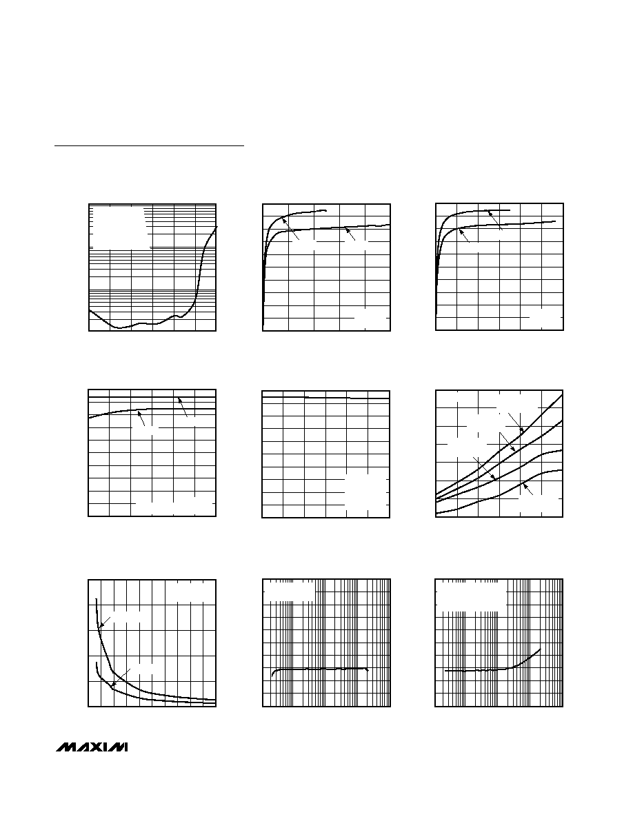
Typical Operating Characteristics
(V
DD
= 3.3V, SYNC = GND (SSM), T
A
= +25°C, unless otherwise noted.)
0.001
10
100k
10k
100
1k
TOTAL HARMONIC DISTORTION PLUS NOISE
vs. FREQUENCY
1
0.1
0.01
MAX9700 toc01
FREQUENCY (Hz)
THD+N (%)
V
DD
= +5V
R
L
= 8
P
OUT
= 300mW
P
OUT
= 125mW
0.001
10
100k
10k
100
1k
TOTAL HARMONIC DISTORTION PLUS NOISE
vs. FREQUENCY
1
0.1
0.01
MAX9700 toc02
FREQUENCY (Hz)
THD+N (%)
V
DD
= +3.3V
R
L
= 8
P
OUT
= 300mW
P
OUT
= 125mW
0.001
10
100k
10k
100
1k
TOTAL HARMONIC DISTORTION PLUS NOISE
vs. FREQUENCY
1
0.1
0.01
MAX9700 toc03
FREQUENCY (Hz)
THD+N (%)
V
DD
= +3.3V
R
L
= 8
P
OUT
= 125mW
SSM MODE
FFM MODE
MAX9700
1.2W, Low-EMI, Filterless,
Class D Audio Amplifier
_______________________________________________________________________________________
5
Typical Operating Characteristics (continued)
(V
DD
= 3.3V, SYNC = GND (SSM), T
A
= +25°C, unless otherwise noted.)
10
0
0.5
1.0
1.5
2.0
2.5
3.0
1
0.1
0.01
TOTAL HARMONIC DISTORTION PLUS NOISE
vs. COMMON-MODE VOLTAGE
MAX9700 toc10
COMMON-MODE VOLTAGE (V)
THD+N (%)
V
DD
= 3.3V
R
L
= 8
f = 1kHz
P
OUT
= 300mW
DIFFERENTIAL INPUT
EFFICIENCY vs. OUTPUT POWER
MAX9700toc11
OUTPUT POWER (W)
EFFICIENCY (%)
1.2
0.9
0.6
0.3
10
20
30
40
50
60
70
80
90
100
0
0
1.5
R
L
= 4
R
L
= 8
V
DD
= 3.3V
f = 1kHz
EFFICIENCY vs. OUTPUT POWER
MAX9700toc12
OUTPUT POWER (W)
EFFICIENCY (%)
2.0
1.5
0.5
10
20
30
40
50
60
70
80
90
100
0
0
3.0
R
L
= 8
R
L
= 4
V
DD
= 5V
f = 1kHz
1.0
2.5
0
30
20
10
50
40
90
80
70
60
100
2.5
3.0
3.5
4.0
4.5
5.0
5.5
EFFICIENCY vs. SUPPLY VOLTAGE
MAX9700 toc13
SUPPLY VOLTAGE (V)
EFFICIENCY (%)
R
L
= 8
f = 1kHz
P
OUT
= MAX (THD+N = 1%)
R
L
= 4
0
30
20
10
50
40
90
80
70
60
100
800
1000
1200
1400
1800
1600
2000
EFFICIENCY
vs. SYNC INPUT FREQUENCY
MAx9700 toc14
SYNC FREQUENCY (kHz)
EFFICIENCY (%)
V
DD
= 3.3V
f = 1kHz
P
OUT
= 300mW
R
L
= 8
OUTPUT POWER vs.
SUPPLY VOLTAGE
MAX9700toc15
SUPPLY VOLTAGE (V)
OUTPUT POWER (W)
5.0
4.5
4.0
3.5
3.0
1.5
2.0
2.5
3.0
3.5
0
2.5
5.5
1.0
0.5
R
L
= 4
THD+N = 10%
R
L
= 4
THD+N = 1%
R
L
= 8
THD+N = 10%
R
L
= 8
THD+N = 1%
f = 1kHz
OUTPUT POWER vs. LOAD RESISTANCE
MAX9700toc16
LOAD RESISTANCE (
)
OUTPUT POWER (mW)
90
80
70
60
50
40
30
20
10
400
800
1200
1600
2000
0
0
100
V
DD
= 5V
f = 1kHz
THD+N = 1%
V
DD
= 3.3V
0
-100
10
100
1k
10k
100k
COMMON-MODE REJECTION RATIO
vs. FREQUENCY
-80
MAX9700TOC17
FREQUENCY (Hz)
CMRR (dB)
-60
-40
-20
-30
-50
-70
-90
-10
INPUT REFERRED
V
IN
= 200mV
P-P
0
-100
10
100
1k
10k
100k
POWER-SUPPLY REJECTION RATIO
vs. FREQUENCY
-80
MAX9700TOC18
FREQUENCY (Hz)
PSRR (dB)
-60
-40
-20
-30
-50
-70
-90
-10
OUTPUT REFERRED
INPUTS AC GROUNDED
V
DD
= 3.3V