 | –≠–ª–µ–∫—Ç—Ä–æ–Ω–Ω—ã–π –∫–æ–º–ø–æ–Ω–µ–Ω—Ç: MAX9724A | –°–∫–∞—á–∞—Ç—å:  PDF PDF  ZIP ZIP |
General Description
The MAX9724A/MAX9724B stereo headphone ampli-
fiers are designed for portable equipment where board
space is at a premium. These devices use a unique,
patented DirectDriveTM architecture to produce a
ground-referenced output from a single supply, elimi-
nating the need for large DC-blocking capacitors, sav-
ing cost, board space, and component height. The
MAX9724A offers an externally adjustable gain while
the MAX9724B has an internally preset gain of -1.5V/V.
The MAX9724A/MAX9724B deliver up to 60mW per
channel into a 32
load and have low 0.02% THD+N.
An 80dB at 1kHz power-supply rejection ratio (PSRR)
allows these devices to operate from noisy digital sup-
plies without an additional linear regulator.
Comprehensive click-and-pop circuitry suppresses
audible clicks and pops on startup and shutdown.
The MAX9724A/MAX9724B operate from a single 2.7V
to 5.5V supply, consume only 3.5mA of supply current,
feature short-circuit and thermal-overload protection,
and are specified over the extended -40∞C to +85∞C
temperature range. The devices are available in tiny 12-
pin Thin QFN (3mm x 3mm x 0.8mm) and 14-pin
TSSOP packages (5mm x 4.4mm x 1.1mm).
Applications
Features
No Bulky DC-Blocking Capacitors Required
Low-Power Shutdown Mode, < 0.1µA
Adjustable Gain (MAX9724A) or Fixed -1.5V/V
Gain (MAX9724B)
Low 0.02% THD+N
High PSRR (80dB at 1kHz) Eliminates LDO
Integrated Click-and-Pop Suppression
2.7V to 5.5V Single-Supply Operation
Low Quiescent Current (3.5mA)
Available in Space-Saving Packages:
12-Pin Thin QFN (3mm x 3mm x 0.8mm)
14-Pin TSSOP (5mm x 4.4mm x 1.1mm)
MAX9724A/MAX9724B
60mW, DirectDrive, Stereo Headphone
Amplifier with Shutdown
________________________________________________________________ Maxim Integrated Products
1
Ordering Information
19-3597; Rev 0; 5/05
For pricing, delivery, and ordering information, please contact Maxim/Dallas Direct! at
1-888-629-4642, or visit Maxim's website at www.maxim-ic.com.
PART
GAIN
(V/V)
PIN-
PACKAGE
PKG
CODE
TOP
MARK
MAX9724AETC+
Adj.
12 TQFN-EP*
T1233-1
AAT
MAX9724AEUD+
Adj.
14 TSSOP
U14-1
--
MAX9724BETC+
-1.5
12 TQFN-EP*
T1233-1
AAU
MAX9724BEUD+
-1.5
14 TSSOP
U14-1
--
Note: All devices specified over the -40∞C to +85∞C operating
range.
+Denotes lead-free package.
*EP = Exposed paddle.
Cellular Phones
MP3 Players
Notebook PCs
Handheld Gaming
Consoles
DVD Players
Smart Phones
PDAs
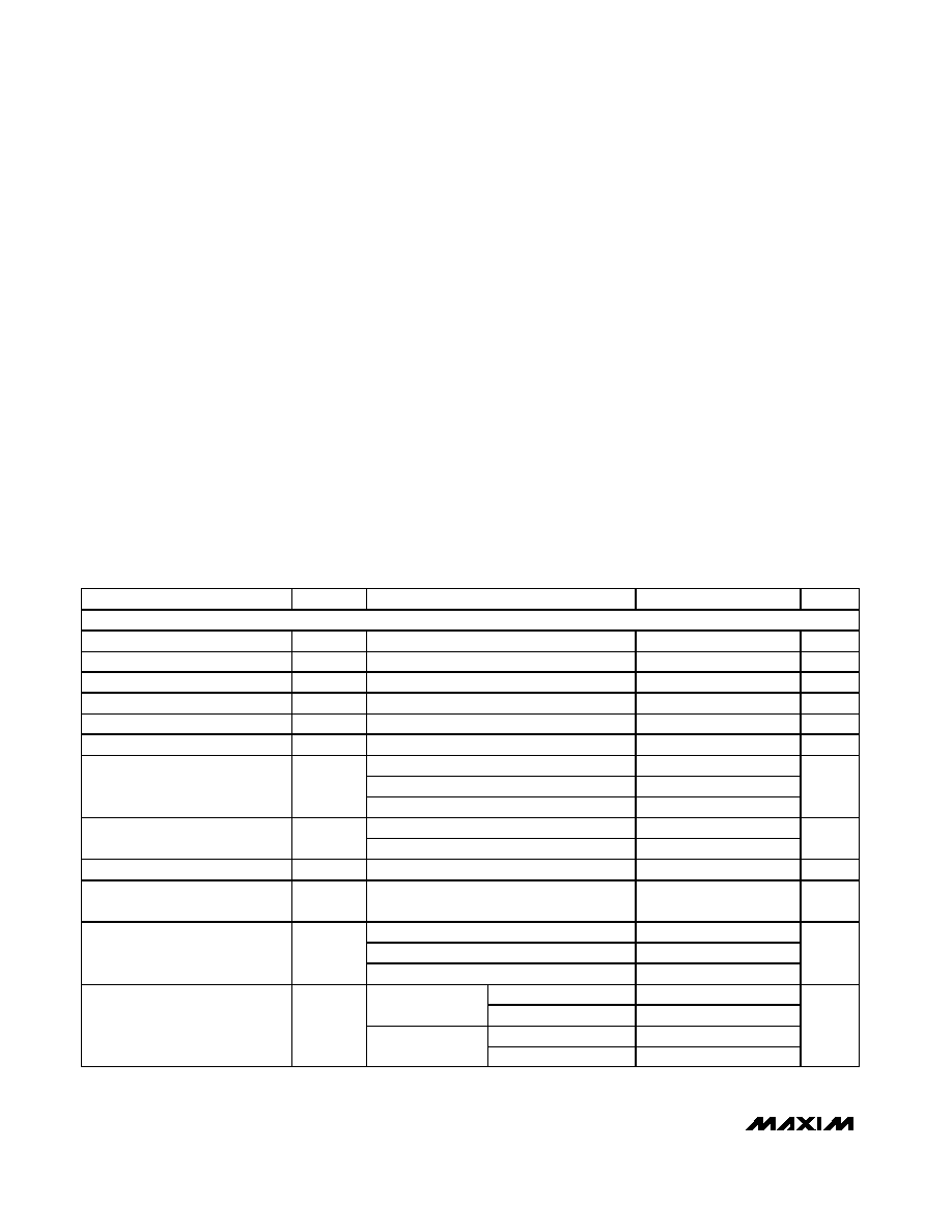
LEFT
AUDIO
INPUT
RIGHT
AUDIO
INPUT
SHDN
MAX9724A
LEFT
AUDIO
INPUT
RIGHT
AUDIO
INPUT
MAX9724B
SHDN
DirectDrive OUTPUTS
ELIMINATE DC-BLOCKING
CAPACITORS
DirectDrive OUTPUTS
ELIMINATE DC-BLOCKING
CAPACITORS
FIXED GAIN ELIMINATES
EXTERNAL RESISTOR
NETWORK
Block Diagrams
Pin Configurations appear at end of data sheet.
MAX9724A/MAX9724B
60mW, DirectDrive, Stereo Headphone
Amplifier with Shutdown
2
_______________________________________________________________________________________
ABSOLUTE MAXIMUM RATINGS
Stresses beyond those listed under "Absolute Maximum Ratings" may cause permanent damage to the device. These are stress ratings only, and functional
operation of the device at these or any other conditions beyond those indicated in the operational sections of the specifications is not implied. Exposure to
absolute maximum rating conditions for extended periods may affect device reliability.
V
DD
to GND ..............................................................-0.3V to +6V
PV
SS
to SV
SS
.........................................................-0.3V to +0.3V
PGND to SGND .....................................................-0.3V to +0.3V
C1P to PGND..............................................-0.3V to (V
DD
+ 0.3V)
C1N to PGND............................................(PV
SS
- 0.3V) to +0.3V
PV
SS
and SV
SS
to PGND..........................................-6V to +0.3V
IN_ to SGND (MAX9724A)..........................-0.3V to (V
DD
+ 0.3V)
IN_ to SGND (MAX9724B) .............(SV
SS
- 0.3V) to (V
DD
+ 0.3V)
OUT_ to SV
SS
(Note 1) ....-0.3V to Min (V
DD
- SV
SS
+ 0.3V, +9V)
OUT_ to V
DD
(Note 2) ......+0.3V to Max (SV
SS
- V
DD
- 0.3V, -9V)
SHDN to _GND.........................................................-0.3V to +6V
OUT_ Short Circuit to GND ........................................Continuous
Short Circuit between OUTL and OUTR ....................Continuous
Continuous Input Current into PV
SS
..................................260mA
Continuous Input Current (any other pin) .........................±20mA
Continuous Power Dissipation (T
A
= +70∞C)
12-Pin TQFN (derate 14.7mW/∞C above +70∞C) .........1177mW
14-Pin TSSOP (derate 9.1mW/∞C above +70∞C) ...........727mW
Operating Temperature Range ...........................-40∞C to +85∞C
Storage Temperature Range .............................-65∞C to +150∞C
Junction Temperature ......................................................+150∞C
Lead Temperature (soldering, 10s) .................................+300∞C
ELECTRICAL CHARACTERISTICS
(V
DD
= 5V, PGND = SGND, SHDN = 5V, C1 = C2 = 1µF, R
L
=
, resistive load reference to ground; for MAX9724A gain = -1.5V/V
(R
IN
= 20k
, R
F
= 30k
); for MAX9724B gain = -1.5V/V (internally set), T
A
= -40∞C to +85∞C, unless otherwise noted. Typical values
are at T
A
= +25∞C, unless otherwise noted.) (Note 3)
PARAMETER
SYMBOL
CONDITIONS
MIN
TYP
MAX
UNITS
GENERAL
Supply Voltage Range
V
DD
Guaranteed by PSRR test
2.7
5.5
V
Quiescent Current
I
CC
3.5
5.5
mA
Shutdown Current
I
SHDN
SHDN = SGND = PGND
<0.1
1
µA
Shutdown to Full Operation
t
SON
180
µs
Input Impedance
R
IN
MAX9724B, measured at IN_
15
19
25
k
Output Offset Voltage
V
OS
(Note 4)
±1.5
±10
mV
V
DD
= 2.7V to 5.5V
69
86
f = 1kHz, 100mV
P-P
(Note 4)
80
Power-Supply Rejection Ratio
PSRR
f = 20kHz, 100mV
P-P
(Note 4)
65
dB
R
L
= 32
, THD+N = 1%
30
63
Output Power
P
OUT
R
L
= 16
, THD+N = 1%
42
mW
Voltage Gain
A
V
MAX9724B (Note 5)
-1.52
-1.5
-1.48
V/V
Channel-to-Channel Gain
Tracking
MAX9724B
±0.15
%
R
L
= 1k
, V
OUT
= 2V
RMS
, f
IN
= 1kHz
0.003
R
L
= 32
, P
OUT
= 50mW, f
IN
= 1kHz
0.02
Total Harmonic Distortion Plus
Noise (Note 6)
THD+N
R
L
= 16
, P
OUT
= 35mW, f
IN
= 1kHz
0.04
%
BW = 22Hz to 22kHz
102
R
L
= 1k
,
V
OUT
= 2V
RMS
A-weighted
105
BW = 22Hz to 22kHz
98
Signal-to-Noise Ratio
SNR
R
L
= 32
,
P
OUT
= 50mW
A-weighted
101
dB
Note 1: OUTR and OUTL should be limited to no more than 9V above SV
SS
, or above V
DD
+ 0.3V, whichever limits first.
Note 2: OUTR and OUTL should be limited to no more than 9V below V
DD
, or below SV
SS
- 0.3V, whichever limits first.
MAX9724A/MAX9724B
60mW, DirectDrive, Stereo Headphone
Amplifier with Shutdown
_______________________________________________________________________________________
3
ELECTRICAL CHARACTERISTICS (continued)
(V
DD
= 5V, PGND = SGND, SHDN = 5V, C1 = C2 = 1µF, R
L
=
, resistive load reference to ground; for MAX9724A gain = -1.5V/V
(R
IN
= 20k
, R
F
= 30k
); for MAX9724B gain = -1.5V/V (internally set), T
A
= -40∞C to +85∞C, unless otherwise noted. Typical values
are at T
A
= +25∞C, unless otherwise noted.) (Note 3)
PARAMETER
SYMBOL
CONDITIONS
MIN
TYP
MAX
UNITS
Slew Rate
SR
0.5
V/µs
Capacitive Drive
C
L
No sustained oscillations
100
pF
Crosstalk
L to R, R to L, f = 10kHz, R
L
= 16
, P
OUT
=
15mW
-70
dB
Charge-Pump Oscillator
Frequency
f
OSC
190
270
400
kHz
Into shutdown
-67
Click-and-Pop Level
K
CP
R
L
= 32
, peak voltage,
A-weighted, 32 samples per
second (Notes 4, 7)
Out of
shutdown
-64
dB
DIGITAL INPUTS (
SHDN)
Input Voltage High
V
INH
2
V
Input Voltage Low
V
INL
0.8
V
Input Leakage Current
±1
µA
ELECTRICAL CHARACTERISTICS
(V
DD
= 3V, PGND = SGND, SHDN = 3V, C1 = C2 = 1µF, R
L
=
, resistive load reference to ground; for MAX9724A gain = -1.5V/V
(R
IN
= 20k
, R
F
= 30k
); for MAX9724B gain = -1.5V/V (internally set), T
A
= -40∞C to +85∞C, unless otherwise noted. Typical values
are at T
A
= +25∞C, unless otherwise noted.) (Note 3)
PARAMETER
SYMBOL
CONDITIONS
MIN
TYP
MAX
UNITS
Quiescent Current
I
CC
3.0
mA
Shutdown Current
I
SHDN
SHDN = SGND = PGND
<0.1
µA
f = 1kHz, 100mV
P-P
80
Power-Supply Rejection Ratio
(Note 4)
PSRR
f = 20kHz, 100mV
P-P
65
dB
R
L
= 32
, THD+N = 1%
20
Output Power
P
OUT
R
L
= 16
, THD+N = 1%
14
mW
R
L
= 1k
, V
OUT
= 2V
RMS
, f
IN
= 1kHz
0.05
R
L
= 32
, P
OUT
= 15mW, f
IN
= 1kHz
0.03
Total Harmonic Distortion Plus
Noise (Note 6)
THD+N
R
L
= 16
, P
OUT
= 10mW, f
IN
= 1kHz
0.06
%
Note 3: All specifications are 100% tested at T
A
= +25∞C; temperature limits are guaranteed by design.
Note 4: The amplifier inputs are AC-coupled to GND.
Note 5: Gain for the MAX9724A is adjustable.
Note 6: Measurement bandwidth is 22Hz to 22kHz.
Note 7: Test performed with a 32
resistive load connected to GND. Mode transitions are controlled by SHDN. K
CP
level is calculat-
ed as 20log[(peak voltage during mode transition, no input signal)/(peak voltage under normal operation at rated power
level)]. Units are expressed in dB.
MAX9724A/MAX9724B
60mW, DirectDrive, Stereo Headphone
Amplifier with Shutdown
4
_______________________________________________________________________________________
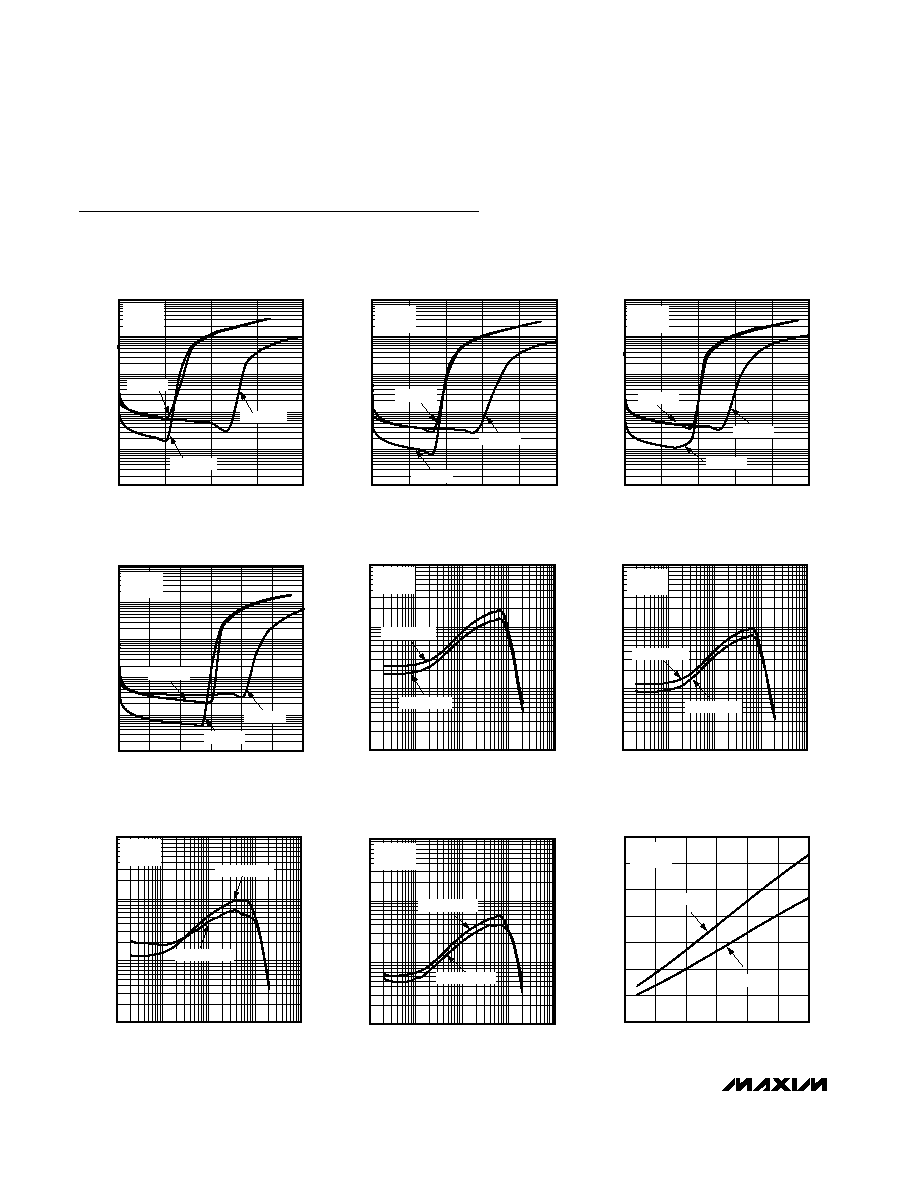
Typical Operating Characteristics
(V
DD
= 5V, PGND = SGND = 0V, SHDN = V
DD
, C1 = C2 = 1µF, R
L
=
, gain = -1.5V/V (R
IN
= 20k
, R
F
= 30k
for the MAX9724A),
THD+N measurement bandwidth = 22Hz to 22kHz, both outputs driven in phase, T
A
= +25∞C, unless otherwise noted.)
100
0
10
20
30
40
10
1
0.1
0.01
0.001
TOTAL HARMONIC DISTORTION PLUS
NOISE vs. OUTPUT POWER
MAX9724toc01
OUTPUT POWER (mW)
THD+N (%)
V
DD
= 3V
R
L
= 16
f
IN
= 1kHz
f
IN
= 20Hz
f
IN
= 10kHz
100
0
10
30
20
40
50
10
1
0.1
0.01
0.001
TOTAL HARMONIC DISTORTION PLUS
NOISE vs. OUTPUT POWER
MAX9724toc02
OUTPUT POWER (mW)
THD+N (%)
V
DD
= 3V
R
L
= 32
f
IN
= 1kHz
f
IN
= 20Hz
f
IN
= 10kHz
100
0
20
60
40
80
100
10
1
0.1
0.01
0.001
TOTAL HARMONIC DISTORTION PLUS
NOISE vs. OUTPUT POWER
MAX9724toc03
OUTPUT POWER (mW)
THD+N (%)
V
DD
= 5V
R
L
= 16
f
IN
= 1kHz
f
IN
= 20Hz
f
IN
= 10kHz
100
0
20
60
40
80
120
10
1
0.1
0.01
0.001
TOTAL HARMONIC DISTORTION PLUS
NOISE vs. OUTPUT POWER
MAX9724toc04
OUTPUT POWER (mW)
THD+N (%)
100
V
DD
= 5V
R
L
= 32
f
IN
= 1kHz
f
IN
= 20Hz
f
IN
= 10kHz
10
1k
100
10k
100k
TOTAL HARMONIC DISTORTION PLUS
NOISE vs. FREQUENCY
MAX9724toc05
FREQUENCY (Hz)
THD+N (%)
1
0.1
0.001
0.01
V
DD
= 3V
R
L
= 16
P
OUT
= 5mW
P
OUT
= 10mW
10
1k
100
10k
100k
TOTAL HARMONIC DISTORTION PLUS
NOISE vs. FREQUENCY
MAX9724toc06
FREQUENCY (Hz)
THD+N (%)
1
0.1
0.001
0.01
V
DD
= 3V
R
L
= 32
P
OUT
= 8mW
P
OUT
= 15mW
10
1k
100
10k
100k
TOTAL HARMONIC DISTORTION PLUS
NOISE vs. FREQUENCY
MAX9724toc07
FREQUENCY (Hz)
THD+N (%)
1
0.1
0.001
0.01
V
DD
= 5V
R
L
= 16
P
OUT
= 20mW
P
OUT
= 37mW
10
1k
100
10k
100k
TOTAL HARMONIC DISTORTION PLUS
NOISE vs. FREQUENCY
MAX9724toc08
FREQUENCY (Hz)
THD+N (%)
1
0.1
0.001
0.01
V
DD
= 5V
R
L
= 32
P
OUT
= 50mW
P
OUT
= 30mW
0
20
10
40
30
60
50
70
2.5
3.5
4.0
3.0
4.5
5.0
5.5
OUTPUT POWER vs. SUPPLY VOLTAGE
MAX9724toc09
SUPPLY VOLTAGE (V)
OUTPUT POWER (mW)
f
IN
= 1kHz
R
L
= 16
1% THD+N
10% THD+N
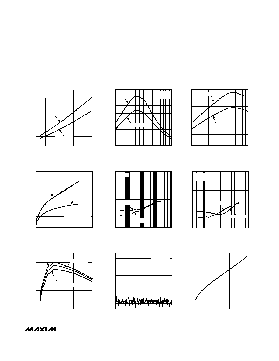
0
40
20
80
60
100
120
2.5
3.5
4.0
3.0
4.5
5.0
5.5
OUTPUT POWER vs. SUPPLY VOLTAGE
MAX9724toc10
SUPPLY VOLTAGE (V)
OUTPUT POWER (mW)
f
IN
= 1kHz
R
L
= 32
1% THD+N
10% THD+N
35
0
10
100
1000
OUTPUT POWER
vs. LOAD RESISTANCE
5
MAX9724toc11
LOAD RESISTANCE (
)
OUTPUT POWER (mW)
15
10
20
25
30
V
DD
= 3V
f
IN
= 1kHz
1% THD+N
10% THD+N
100
0
10
100
OUTPUT POWER
vs. LOAD RESISTANCE
10
MAX9724toc12
LOAD RESISTANCE (
)
OUTPUT POWER (mW)
30
20
50
70
90
40
60
80
THD+N = 1%
V
DD
= 5V
f
IN
= 1kHz
THD+N = 10%
0
50
150
100
200
250
POWER DISSIPATION
vs. OUTPUT POWER
MAX9724toc13
OUTPUT POWER (mW)
POWER DISSIPATION (mW)
0
40
20
60
80
V
DD
= 3V
f
IN
= 1kHz
P
OUT
= P
OUTL
+ P
OUTR
OUTPUTS IN PHASE
R
L
= 16
R
L
= 32
0
-120
10
100
10k
100k
POWER-SUPPLY REJECTION
RATIO vs. FREQUENCY
-100
-80
-40
-60
-20
MAX9724toc14
FREQUENCY (Hz)
PSRR (dB)
1k
V
DD
= 5V
V
DD
= 3V
R
L
= 32
0
-120
10
100
10k
100k
CROSSTALK vs. FREQUENCY
-100
-80
-40
-60
-20
MAX9724toc15
FREQUENCY (Hz)
CROSSTALK (dB)
1k
RIGHT TO LEFT
LEFT TO RIGHT
P
OUT
= 15mW
R
L
= 16
20
40
30
60
50
70
80
0
100
150
50
OUTPUT POWER vs. LOAD RESISTANCE
AND CHARGE-PUMP CAPACITOR SIZE
MAX9724toc16
LOAD RESISTANCE (
)
OUTPUT POWER (mW)
V
DD
= 5V
f
IN
= 1kHz
THD+N = 1%
C1 = C2 = 2.2
µF
C1 = C2 = 1
µF
C1 = C2 = 0.47
µF
-140
-110
-130
-70
-90
-50
-120
-80
-100
-60
-40
0
5
10
15
20
OUTPUT SPECTRUM
vs. FREQUENCY
MAX9724toc17
FREQUENCY (kHz)
AMPLITUDE (dBV)
R
L
= 32
V
DD
= 3V
f
IN
= 1kHz
V
OUT
= -60dBV
2.8
3.1
2.9
3.3
3.0
3.4
3.2
3.5
2.5
3.0
4.0
3.5
4.5
5.0
5.5
SUPPLY CURRENT
vs. SUPPLY VOLTAGE
MAX9724toc18
SUPPLY VOLTAGE (V)
SUPPLY CURRENT (mA)
NO LOAD
INPUTS
GROUND
Typical Operating Characteristics (continued)
(V
DD
= 5V, PGND = SGND = 0V, SHDN = V
DD
, C1 = C2 = 1µF, R
L
=
, gain = -1.5V/V (R
IN
= 20k
, R
F
= 30k
for the MAX9724A),
THD+N measurement bandwidth = 22Hz to 22kHz, both outputs driven in phase, T
A
= +25∞C, unless otherwise noted.)
MAX9724A/MAX9724B
60mW, DirectDrive, Stereo Headphone
Amplifier with Shutdown
_______________________________________________________________________________________
5