 | –≠–ª–µ–∫—Ç—Ä–æ–Ω–Ω—ã–π –∫–æ–º–ø–æ–Ω–µ–Ω—Ç: MAX9757 | –°–∫–∞—á–∞—Ç—å:  PDF PDF  ZIP ZIP |

General Description
The MAX9756/MAX9757/MAX9758 combine dual, 2.3W,
bridge tied load (BTL) stereo audio power amplifiers and
a DirectDrive
TM
headphone amplifier in a single device.
These devices feature single-supply voltage operation,
shutdown mode, logic-selectable gain, a headphone
sense input, a 31-step analog volume control, and indus-
try-leading click-and-pop suppression. The headphone
amplifier uses Maxim's patent-pending DirectDrive archi-
tecture that produces a ground-referenced output from a
single supply, eliminating the need for large DC-blocking
capacitors.
The MAX9756/MAX9757 feature automatic level control
(ALC) that automatically limits output power to the speak-
er in the event of an overpowered output.
The MAX9756/MAX9758s' 150mA internal linear regula-
tor provides a complete solution for DAC- or CODEC-
based designs.
The MAX9756/MAX9757/MAX9758 are offered in space-
saving, thermally efficient 32-pin (5mm x 5mm x 0.8mm)
and 36-pin thin QFN (6mm x 6mm x 0.8mm) packages.
All devices are specified over the extended -40∞C to
+85∞C temperature range.
Features
Automatic Level Control--Protects Speakers
Analog Volume Control
120mW DirectDrive Headphone Amplifiers (16)
150mA Adjustable LDO
Class AB, 2.3W, Stereo BTL Speaker Amplifiers
(3
)
High 95dB PSRR
Low-Power Shutdown Mode
Industry-Leading Click-and-Pop Suppression
Short-Circuit and Thermal Protection
Beep Input
MAX9756/MAX9757/MAX9758
2.3W Stereo Speaker Amplifiers and DirectDrive
Headphone Amplifiers with Automatic Level Control
________________________________________________________________ Maxim Integrated Products
1
VOL
ALC
SINGLE SUPPLY 4.5V TO 5.5V
SINGLE SUPPLY 4.5V TO 5.5V
SINGLE SUPPLY 4.5V TO 5.5V
1.2V TO 5V
HPS
BEEP
MAX9756
LDO
ALC
VOL
ALC
HPS
BEEP
MAX9757
ALC
VOL
1.2V TO 5V
HPS
BEEP
MAX9758
LDO
Simplified Block Diagrams
Ordering Information
Applications
PART
ALC
LDO
PIN-PACKAGE
MAX9756ETX+
36 Thin QFN-EP**
MAX9757ETJ+*
--
32 Thin QFN-EP**
MAX9758ETJ+*
--
32 Thin QFN-EP**
19-3782; Rev 0; 8/05
For pricing, delivery, and ordering information, please contact Maxim/Dallas Direct! at
1-888-629-4642, or visit Maxim's website at www.maxim-ic.com.
EVALUATION KIT
AVAILABLE
Notebook PCs
Tablet PCs
Portable DVD
Players
Flat-Panel TVs
PC Displays
LCD Projectors
Portable Audio
Note: All devices specified for -40∞C to +85∞C operating
temperature range.
+Denotes lead-free package.
*Future product--contact factory for availability.
**EP = Exposed paddle.

MAX9756/MAX9757/MAX9758
2.3W Stereo Speaker Amplifiers and DirectDrive
Headphone Amplifiers with Automatic Level Control
2
_______________________________________________________________________________________
ABSOLUTE MAXIMUM RATINGS
ELECTRICAL CHARACTERISTICS
(V
DD
= PV
DD
= HPV
DD
= CPV
DD
= IN = +5.0V, GND = PGND = CPGND = 0,
SHDN = V
DD
, REGEN = V
DD
, DR = SET = GND, C
BIAS
= 1µF, C
PVSS
= 1µF, C1 = C2 = 1µF, PREF = unconnected, speaker loads terminated between OUT_+ and OUT_-, headphone load
terminated between HP_ and GND, GAIN1 = GAIN2 = GAIN3 = VOL = 0 (A
V(SP)
= 15dB, A
V(HP)
= 0dB), T
A
= -40∞C to +85∞C, unless
otherwise noted. Typical values are at T
A
= +25∞C.) (Note 1)
Stresses beyond those listed under "Absolute Maximum Ratings" may cause permanent damage to the device. These are stress ratings only, and functional
operation of the device at these or any other conditions beyond those indicated in the operational sections of the specifications is not implied. Exposure to
absolute maximum rating conditions for extended periods may affect device reliability.
Supply Voltage (V
DD
, PV
DD
, HPV
DD
, CPV
DD
, IN to GND) ....+6V
PGND, CPGND to GND ......................................................±0.3V
CPV
SS
, C1N, V
SS
to GND......................................-6.0V to +0.3V
HP_ to GND ...........................................................................±3V
Any Other Pin .............................................-0.3V to (V
DD
+ 0.3V)
Duration of OUT_ Short Circuit to GND or PV
DD
........Continuous
Duration of OUT_+ Short Circuit to OUT_- .................Continuous
Duration of HP_ Short Circuit to GND,
V
SS
, or HPV
DD
.........................................................Continuous
Duration of OUT Short Circuit to GND........................Continuous
Continuous Current (PV
DD
, OUT_, PGND) ...........................1.7A
Continuous Current (CPV
DD
, C1N, CPGND, C1P, CPV
SS
,
V
SS
, HPV
DD
, HP_, IN, OUT) .............................................0.85A
Continuous Input Current (all other pins) .........................±20mA
Continuous Power Dissipation (T
A
= +70∞C, single-layer board)
32-Pin Thin QFN (derate 18.6mW/∞C above +70∞C).....1490mW
36-Pin Thin QFN (derate 20.4mW/∞C above +70∞C).....1633mW
Continuous Power Dissipation (T
A
=+70∞C, multilayer board)
32-Pin Thin QFN (derate 24.9mW/∞C above +70∞C).....1990mW
36-Pin Thin QFN (derate 27.7mW/∞C above +70∞C).....2180mW
Junction Temperature .....................................................+150∞C
Operating Temperature Range ...........................-40∞C to +85∞C
Storage Temperature Range .............................-65∞C to +150∞C
Lead Temperature (soldering, 10s) .................................+300∞C
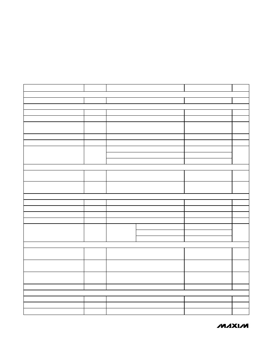
PARAMETER
SYMBOL
CONDITIONS
MIN
TYP
MAX
UNITS
GENERAL
Supply Voltage Range
V
DD
, PV
DD
Inferred from PSRR test
4.5
5.5
V
Headphone Supply Voltage
HPV
DD
Inferred from PSRR test
3.0
5.5
V
HPS = GND, speaker
mode, R
L
=
14
29
Quiescent Supply Current
I
DD
I
DD
= I
VDD
+
I
HPVDD
+ I
CPVDD
HPS = 5V, headphone
mode, R
L
=
7
13
mA
Shutdown Supply Current
I
SHDN
SHDN = REGEN = GND
0.2
5
µA
Bias Voltage
V
BIAS
2.2
2.43
2.65
V
Switching Time
t
SW
Gain or input switching
10
µs
Input Resistance
R
IN
INL and INR
10
20
30
k
Turn-On Time
t
SON
25
ms
SPEAKER AMPLIFIERS (HPS = GND)
Output Offset Voltage
V
OS
Measured between OUT_+ and OUT_-,
T
A
= +25∞C
±0.4
±15
mV
PV
DD
= 4.5V to 5.5V, T
A
= +25∞C
75
95
f = 1kHz, V
RIPPLE
= 200mV
P-P
83
Power-Supply Rejection Ratio
(Note 2)
PSRR
f = 10kHz, V
RIPPLE
= 200mV
P-P
68
dB
R
L
= 8
0.9
1.3
R
L
= 4
2.0
Output Power (Note 3)
P
OUT
THD+N = 1%, f = 1kHz
(T
A
= +25∞C)
R
L
= 3
2.3
W
R
L
= 8
, BTL P
OUT
= 1W, f = 1kHz
0.009
Total Harmonic Distortion Plus
Noise
THD+N
R
L
= 4
, BTL P
OUT
= 1W, f = 1kHz
0.015
%
R
L
= 8
, BTL P
OUT
= 1W, BW = 22Hz to
22kHz, unweighted
92
Signal-to-Noise Ratio
SNR
R
L
= 8
, BTL P
OUT
= 1W, A weighted
95
dB

MAX9756/MAX9757/MAX9758
2.3W Stereo Speaker Amplifiers and DirectDrive
Headphone Amplifiers with Automatic Level Control
_______________________________________________________________________________________
3
ELECTRICAL CHARACTERISTICS (continued)
(V
DD
= PV
DD
= HPV
DD
= CPV
DD
= IN = +5.0V, GND = PGND = CPGND = 0,
SHDN = V
DD
, REGEN = V
DD
, DR = SET = GND, C
BIAS
= 1µF, C
PVSS
= 1µF, C1 = C2 = 1µF, PREF = unconnected, speaker loads terminated between OUT_+ and OUT_-, headphone load
terminated between HP_ and GND, GAIN1 = GAIN2 = GAIN3 = VOL = 0 (A
V(SP)
= 15dB, A
V(HP)
= 0dB), T
A
= -40∞C to +85∞C, unless
otherwise noted. Typical values are at T
A
= +25∞C.) (Note 1)
PARAMETER
SYMBOL
CONDITIONS
MIN
TYP
MAX
UNITS
Noise
V
n
BW = 22Hz to 22kHz, unweighted,
measured at output, input at AC GND
71
µV
RMS
Capacitive-Load Drive
C
L
No sustained oscillations
200
pF
Crosstalk
L to R, R to L, f = 10kHz
80
dB
Slew Rate
SR
Measured between OUT_+ and OUT_-
1.3
V/µs
GAIN3 = 0
GAIN2 = 0
GAIN1 = 0
15
GAIN3 = 0
GAIN2 = 0
GAIN1 = 1
16.5
GAIN3 = 0
GAIN2 = 1
GAIN1 = 0
18
GAIN3 = 0
GAIN2 = 1
GAIN1 = 1
19.5
GAIN3 = 1
GAIN2 = 0
GAIN1 = 0
21
GAIN3 = 1
GAIN2 = 0
GAIN1 = 1
22.5
GAIN3 = 1
GAIN2 = 1
GAIN1 = 0
24.0
Gain (Maximum Volume Settings)
(Note 4)
A
VMAX
(SPKR)
GAIN3 = 1
GAIN2 = 1
GAIN1 = 1
25.5
dB
Into
shutdown
65
Click-and-Pop Level
K
CP
Peak voltage, 32
samples/second,
A weighted (Note 5)
Out of
shutdown
38.5
dBV
HEADPHONE AMPLIFIERS (HPS = V
DD
)
Output Offset Voltage
V
OS(HP)
T
A
= +25∞C
±2
±7
mV
HPV
DD
= 3V to 5.5V, T
A
= +25∞C
70
90
f = 1kHz, V
RIPPLE
= 200mV
P-P
72
Power-Supply Rejection Ratio
(Note 2)
PSRR
f = 10kHz, V
RIPPLE
= 200mV
P-P
70
dB
R
L
= 32
40
68
Output Power (Note 3)
P
OUT
THD+N = 1%, f = 1kHz
(T
A
= +25∞C)
R
L
= 16
130
mW
R
L
= 32
, V
OUT
= 1V
RMS
, f = 1kHz
0.02
Total Harmonic Distortion Plus
Noise
THD+N
R
L
= 16
, V
OUT
= 1V
RMS
, f = 1kHz
0.04
%
R
L
= 32
, BTL P
OUT
= 65mW,
BW = 22Hz to 22kHz, unweighted
97
Signal-to-Noise Ratio
SNR
R
L
= 32
, BTL P
OUT
= 65W,
BW = 22Hz to 22kHz, A weighted
100
dB
Noise
V
n
BW = 22Hz to 22kHz
20.4
µV
RMS
Capacitive-Load Drive
C
L
No sustained oscillations
200
pF
Crosstalk
L to R, R to L, f = 10kHz
60
dB
Slew Rate
SR
1.4
V/µs
GAIN2 = 0, HPS = 1
0
Gain (Maximum Volume Settings)
(Note 6)
A
VMAX(HP)
GAIN2 = 1, HPS = 1
3.0
dB
Into shutdown
62
Click-and-Pop Level
K
CP
Peak voltage, 32
samples/second,
A weighted (Note 4)
Out of shutdown
50
dBV
MAX9756/MAX9757/MAX9758
2.3W Stereo Speaker Amplifiers and DirectDrive
Headphone Amplifiers with Automatic Level Control
4
_______________________________________________________________________________________
ELECTRICAL CHARACTERISTICS (continued)
(V
DD
= PV
DD
= HPV
DD
= CPV
DD
= IN = +5.0V, GND = PGND = CPGND = 0,
SHDN = V
DD
, REGEN = V
DD
, DR = SET = GND, C
BIAS
= 1µF, C
PVSS
= 1µF, C1 = C2 = 1µF, PREF = unconnected, speaker loads terminated between OUT_+ and OUT_-, headphone load
terminated between HP_ and GND, GAIN1 = GAIN2 = GAIN3 = VOL = 0 (A
V(SP)
= 15dB, A
V(HP)
= 0dB), T
A
= -40∞C to +85∞C, unless
otherwise noted. Typical values are at T
A
= +25∞C.) (Note 1)
PARAMETER
SYMBOL
CONDITIONS
MIN
TYP
MAX
UNITS
CHARGE PUMP
Charge-Pump Frequency
f
OSC
500
550
600
kHz
VOLUME CONTROL
VOL Input Impedance
R
VOL
100
M
VOL Input Hysteresis
10
mV
Full Mute Voltage
(Note 7)
0.858 x
HPV
DD
V
Full Mute Attenuation
f
IN
= 1kHz
-85
dB
Input Impedance
R
VOL_
Any gain setting
100
M
A
V
= +15dB to 0dB
±0.2
A
V
= -2dB to -20dB
±0.3
Channel Matching
A
V
= -22dB to -56dB
±1.0
dB
BEEP INPUT
Beep Signal Amplitude Threshold
T
A
= +25∞C, R
B
= 47k
(see BEEP Input
section)
0.3
V
Beep Signal Frequency
Threshold
T
A
= +25∞C
300
Hz
AUTOMATIC LEVEL CONTROL SPEAKER AMPLIFIER (MAX9756/MAX9757)
PREF Threshold Accuracy
R
PREF
= 180k
5
8.1
%
Maximum Gain Compression
6.0
6.3
dB
Attack Time
C
T
= 1µF (Note 8)
15
ms
Hold Time
Time between attack and release phases
50
ms
0V < V
DR
< (0.3V x V
DD
)
30
0.4V < V
DR
< (0.6V x V
DD
)
9.5
Release Time (Note 9)
C
T
= 1µF,
release from
6dB
0.8V < V
DR
< V
DD
3
s
DR INPUT (TRI-STATE INPUT)
DR Input Voltage High
V
DRH
0.8 x
V
DD
V
DD
V
DR Input Voltage Middle
V
DRM
0.4 x
V
DD
0.6 x
V
DD
V
DR Input Voltage Low
V
DRL
0
0.3 x
V
DD
V
Input Leakage Current
0V
V
DR
V
DD
±1
µA
LOGIC INPUTS (GAIN_,
SHDN, REGEN)
Input High Voltage
V
IH
2
V
Input Low Voltage
V
IL
0.8
V
Input Leakage Current
I
IN
±1
µA

MAX9756/MAX9757/MAX9758
2.3W Stereo Speaker Amplifiers and DirectDrive
Headphone Amplifiers with Automatic Level Control
_______________________________________________________________________________________
5
Note 1:
All devices are 100% production tested at room temperature. All temperature limits are guaranteed by design.
Note 2:
PSRR is specified with the amplifier input connected to GND through R
IN
and C
IN
.
Note 3:
Output power levels are measured with the TQFN's exposed paddle soldered to the ground plane.
Note 4:
Speaker path gain is defined as: A
VSPKR
= (V
OUT+
- V
OUT-
)/V
IN__
).
Note 5:
Speaker mode testing performed with 8
resistive load connected across BTL output. Headphone mode testing per-
formed with 32
resistive load connected between HP_ and GND. Mode transitions are controlled by SHDN.
Note 6:
Headphone path gain is defined as: A
VHP
= V
HP_
/V
IN__
.
Note 7:
See Table 3 for detains on the mute levels.
Note 8:
Attack envelope is exponential. Attack time is defined as the 15 x 10
3
x C
T
.
Note 9:
Time for the gain to return to within 10% of nominal gain setting after the input signal has fallen below the PREF threshold.
Release is linear in dB. Release time is proportional to magnitude of gain compression.
Note 10: Dropout voltage is defined as (V
IN
- V
OUT
) when V
OUT
is 2% below the value of V
OUT
for V
IN
= V
OUT(NOM)
+ 1V.
ELECTRICAL CHARACTERISTICS (continued)
(V
DD
= PV
DD
= HPV
DD
= CPV
DD
= IN = +5.0V, GND = PGND = CPGND = 0,
SHDN = V
DD
, REGEN = V
DD
, DR = SET = GND, C
BIAS
= 1µF, C
PVSS
= 1µF, C1 = C2 = 1µF, PREF = unconnected, speaker loads terminated between OUT_+ and OUT_-, headphone load
terminated between HP_ and GND, GAIN1 = GAIN2 = GAIN3 = VOL = 0 (A
V(SP)
= 15dB, A
V(HP)
= 0dB), T
A
= -40∞C to +85∞C, unless
otherwise noted. Typical values are at T
A
= +25∞C.) (Note 1)
PARAMETER
SYMBOL
CONDITIONS
MIN
TYP
MAX
UNITS
LOGIC INPUT HEADPHONE (HPS)
Input High Voltage
V
IH
2
V
Input Low Voltage
V
IL
0.8
V
HPS Pullup Current
35
µA
LOW-DROPOUT LINEAR REGULATOR
Input Voltage Range
V
IN
Inferred from line regulation
3.5
5.5
V
I
OUT
= 0mA,
SHDN = GND
100
160
Supply (Ground) Current
I
Q
I
OUT
= 150mA
350
µA
Shutdown Current
I
SHDN
REGEN = 0V
0.1
3
µA
Output Current
I
OUT
150
mA
Fixed Output Voltage Accuracy
I
OUT
= 1mA
±1.5
%
Adjustable Output Voltage Range
V
SET
4.85
V
SET Reference Voltage
V
SET
1.19
1.21
1.23
V
SET Dual-Mode Threshold
200
mV
SET Input Leakage Current
I
SET
±20
±500
nA
I
OUT
= 50mA
25
50
Dropout Voltage (Note 10)
V
OD
V
OUT
= 4.65V (fixed
output operation)
I
OUT
= 150mA
100
150
mV
Output Current Limit
I
LIM
300
mA
Startup Time
20
µs
Line Regulation
V
IN
= 3.5V to 5.5V, V
OUT
= 2.5V,
I
OUT
= 1mA
-0.1
+0.01
+0.1
%/V
Load Regulation
V
OUT
= 4.65V, 1mA < I
OUT
< 150mA
0.5
%
f = 1kHz
60
Ripple Rejection
V
RIPPLE
= 200mV
P-P
f = 10kHz
50
dB
Output Voltage Noise
20Hz to 22kHz, C
OUT
= 2 x 1µF,
I
OUT
= 150mA, V
OUT
= 4.65V
100
µV
RMS