
General Description
The MAX9760 evaluation system (EV system) consists
of a MAX9760 evaluation kit (EV kit) and a companion
Maxim System Management Bus (SMBusTM) interface
board. The MAX9760 EV kit is also capable of evaluat-
ing the MAX9761/MAX9762/MAX9763.
The MAX9760 EV kit is a fully assembled and tested
surface-mount circuit board that evaluates the
MAX9760 3W stereo audio power amplifier plus head-
phone driver. The EV kit is designed to be driven by
any stereo audio source such as a CD player. The EV
kit includes RCA jacks on the inputs, a 3.5mm head-
phone jack, and terminal blocks on the outputs to facili-
tate easy connections to the circuit board. The EV kit
includes Windows
Æ
98/2000/XP-compatible software,
which provides a user interface for exercising the
MAX9760's features.
The Maxim SMBus interface board (MAXSMBUS) allows
an IBM-compatible PC to use its parallel port to emulate
an SMBus/I
2
CTM 2-wire interface. Windows 98/2000/XP-
compatible software provides a user-friendly interface to
exercise the MAX9760 features. The program is menu
driven and offers a graphical user interface (GUI) with
control buttons and a status display.
The MAX9760EVSYS includes both the EV kit and the
MAXSMBUS interface board. Order the MAX9760EVKIT
if you already have an SMBus interface.
Features
o 4.5V to 5.5V Single-Supply Operation
o 3W Stereo Bridge-Tied-Load (BTL) Amplifier
o 100dB Power-Supply Rejection Ratio
o SMBus/I
2
C-Compatible 2-Wire Serial Interface
o 2:1 Stereo Input MUX
o Selectable Bass-Boost Circuitry
o No Detectable Clicks or Pops
o Easy-to-Use, Menu-Driven Software
o Assembled and Tested
o Software-Controlled Mute, Shutdown, Input
Selection, and Gain
o Automatic Headphone-Sensing Circuitry
o Includes Windows 98/2000/XP-Compatible
Software and Demo PC Board
o Evaluates the MAX9761/MAX9762/MAX9763
Evaluates: MAX9760--MAX9763
MAX9760 Evaluation System/Evaluation Kit
________________________________________________________________ Maxim Integrated Products
1
19-2833; Rev 0; 4/03
For pricing, delivery, and ordering information, please contact Maxim/Dallas Direct! at
1-888-629-4642, or visit Maxim's website at www.maxim-ic.com.
Ordering Information
PART
TEMP RANGE
IC
PACKAGE
SMBus
INTERFACE
TYPE
MAX9760EVKIT
0∞C to +70∞C
28 QFN
Not included
MAX9760EVSY
0∞C to +70∞C
28 QFN
MAXSMBUS
SMBus is a trademark of Intel Corp.
Windows is a registered trademark of Microsoft Corp.
I
2
C is a trademark of Philips Corp. Purchase of I
2
C compo-
nents of Maxim Integrated Products, Inc., or one of its subli-
censed Associated Companies, conveys a license under the
Philips I
2
C Patent Rights to use these components in an I
2
C
system, provided that the system conforms to the I
2
C Standard
Specification as defined by Philips.
Note: To evaluate the MAX9761, MAX9762, or MAX9763,
request a MAX9761ETI, MAX9762ETI, or MAX9763ETI free sam-
ple with the MAX9760EVKIT. The MAX9760 EV kit software is
provided with the MAX9760EVKIT; however, the MAXSMBUS
board is required to interface the EV kit to the computer when
using the included software.
SINGLE SUPPLY
4.5V TO 5.5V
MAX9760EVKIT
INPUT L1
INPUT L2
INPUT R1
INPUT R2
HPS
I
2
C
COMPATIBLE
SE/
BTL
LEFT
RIGHT
SMBUS/I
2
C-
COMPATIBLE
INTERFACE
Figure 1. MAX9760 EV Kit Block Diagram
Block Diagram
Evaluates: MAX9760--MAX9763
Quick Start
Recommended Equipment
∑ Computer running Windows 98, 2000, or XP
∑ Parallel printer port (this is a 25-pin socket on the
back of the computer)
∑ Standard 25-pin, straight-through, male-to-female
cable (printer extension cable) to connect the comput-
er's parallel port to the Maxim SMBus interface board
∑ 9V/100mA DC power supply (for the SMBus card)
∑ 5V/4A DC power supply
∑ One pair of headphones (16
or greater)
∑ Two stereo audio sources (to demonstrate the input
mux feature)
∑ One pair of speakers (3
or greater)
Procedure
The MAX9760 EV kit is fully assembled and tested. Follow
the steps below to verify board operation. Do not turn on
the power supply until all connections are completed:
1) Carefully connect the boards by aligning the 20-pin
connector of the MAX9760 EV kit with the 20-pin
header of the MAXSMBUS interface board. Gently
press them together.
2) Ensure that a shunt is placed across pins 1 and 2 of
jumpers JU1, JU4, and JU5.
3) Ensure that jumpers JU2 and JU3 do not have a
shunt placed on them.
4) Ensure that a shunt is installed on jumper JU6.
5) Connect a cable from the computer's parallel port to
the SMBus interface board. Use a straight-through
MAX9760 Evaluation System/Evaluation Kit
2
_______________________________________________________________________________________
Component List
DESIGNATION
QTY
DESCRIPTION
C1≠C4
4
0.68µF ±10%, 20V tantalum
capacitors (R-case)
AVX TAJR684K020
C5, C6, C16
3
100pF ±5%, 50V C0G ceramic
capacitors (0402)
TDK C1005C0G1H101J
C7, C8
2
0.047µF ±10%, 16V X7R ceramic
capacitors (0402)
TDK C1005X7R1C473K
C9, C10, C11,
C14, C15
5
220µF ±20%, 6.3V tantalum
capacitors (C-case)
AVX TPSC227M006R0250
C12, C13
2
1.0µF ±20%, 10V X7R ceramic
capacitors (0603)
TDK C1608X7R1A105M
R1≠R6, R18
7
15.0k
±1% resistors (0402)
R7, R8
2
33.2k
±1% resistors (0402)
R9, R10
2
27.4k
±1% resistors (0402)
R11, R12, R15,
R16
4
10k
±5% resistors (0402)
DESIGNATION
QTY
DESCRIPTION
R13, R14
2
1k
±5% resistors (0402)
R17
1
680k
±5% resistor (0402)
R19
1
47k
±5% resistor (0402)
J1, J3
2
Phono jacks, white
J2, J4
2
Phono jacks, red
J5
1
Switched stereo headphone jack
(3.5mm dia)
J6
1
2 x 10 right-angle female receptacle
JU1
1
Jumper, dual row, 12-pin header
JU2≠JU5
4
3-pin headers
JU6
1
2-pin header
JU7
0
Not installed (SIP-3)
TB1, TB2
2
2-circuit terminal blocks
U1
1
MAX9760ETI (28-pin QFN)
None
6
Shunts
None
1
MAX9760 PC Board
None
1
Software disk (CD-ROM)
MAX9760 Evaluation Kit
Component Suppliers
SUPPLIER
PHONE
FAX
WEBSITE
AVX
843-946-0238
843-626-3123
www.avxcorp.com
TDK
847-803-6100
847-390-4405
www.component.tdk.com
Note: Please indicate that you are using the MAX9760 when contacting these component suppliers.
25-pin male-to-female cable. To avoid damaging
the EV kit or your computer, do not use a 25-pin
SCSI port or any other connector that is physically
similar to the 25-pin parallel printer port.
6) The MAX9760.EXE software program can be run
from the CD-ROM or hard drive. Use the Windows
program manager to run the program. If desired,
you may use the INSTALL.EXE program to copy the
files and create icons in the Windows 98/2000/XP
Start menu.
Do not turn on the power until all connections
are made.
7) Connect the 9V power supply to the pads labeled
POS9 and GND1 of the SMBus interface board.
8) Connect the 5.0V power supply to the pads labeled
VDD and GND on the MAX9760 EV kit board.
9) Ensure that both stereo audio sources are turned off.
10) Connect the first stereo audio source to the input
jacks labeled J1 and J2.
11) Connect the second stereo audio source to the
input jacks labeled J3 and J4.
12) Plug the headphones into the 3.5mm headphone
jack labeled J5.
13) Connect the speakers to the terminal blocks labeled
TB1 and TB2.
14) Turn on the DC power supplies.
15) Enable the stereo audio sources.
16) Start the MAX9760 program by opening its icon in
the Start menu.
17) Normal device operation can be verified by the SMBus
Status: DUT Board Found text in the Interface box.
Evaluates: MAX9760--MAX9763
MAX9760 Evaluation System/Evaluation Kit
_______________________________________________________________________________________
3
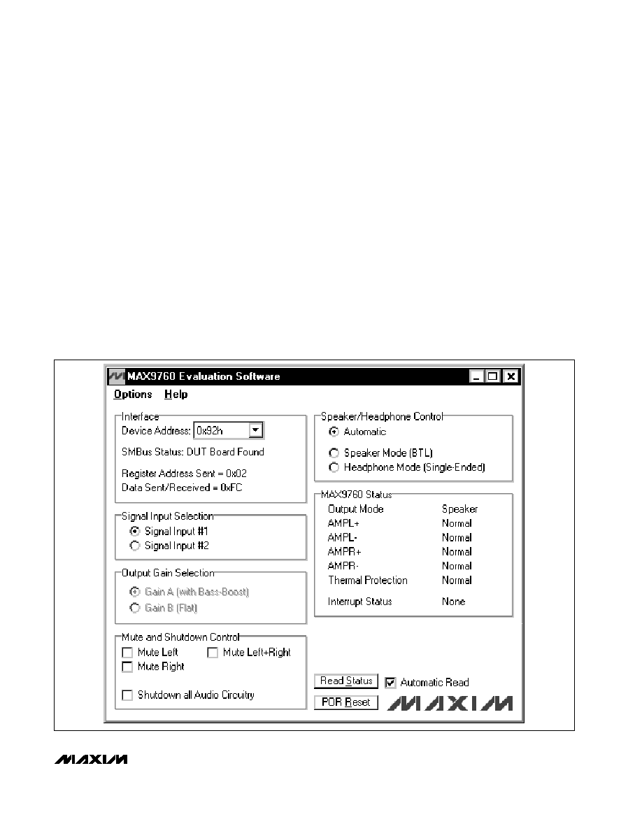
Figure 2. MAX9760 EV Kit Software Main Window

Evaluates: MAX9760--MAX9763
Detailed Description of
Software
User-Interface Panel
The user interface (shown in Figure 2) is easy to operate;
use the mouse, or a combination of the Tab and Arrow
keys to manipulate the software. Each of the buttons
corresponds to bits in the command and configuration
bytes. By clicking on them, the correct SMBus write
operation is generated to update the internal registers of
the MAX9760. The Interface box indicates the current
Device Address, the Register Address, and the Data
Sent/Received for the last read/write operation. This
data is used to confirm proper device operation.
Note: Words in boldface are user-selectable features in
the software.
Signal Input Selection
The MAX9760 EV kit can route one of two independent
stereo signals to the speakers or headphones. The
input signal is selected by choosing the desired option
in the Signal Input Selection box. Choosing Signal
Input #1, routes the signal from input jacks J1 and J2.
Choosing Signal Input #2, routes the signal from input
jacks J3 and J4.
MAX9760 Status
The program continually polls the device for new status
data and monitors the alert conditions. To disable contin-
uous polling of data, uncheck the Automatic Read
checkbox. If an interrupt condition is generated by the
headphones being inserted, the message INTERRUPT
appears.
Speaker/Headphone Control
Selecting the desired option in the Speaker/Headphone
Control box allows the MAX9760 EV kit to operate in one
of three independent modes. The Automatic mode
(default) detects the insertion of the headphones in jack
J5. The speaker outputs are disabled if the headphones
are present, and enabled if the headphones are absent.
Selecting the Speaker Mode (BTL) provides drive to the
speakers and headphones (if both are present). Selecting
the Headphone Mode (Single-Ended) provides drive to
the headphones only.
Software Mute and Shutdown Control
Selecting the desired option in the Mute and Shutdown
Control box allows the MAX9760 EV kit to disable the left,
right, or both output channels. Checking the Mute Left
option mutes the left channel. Checking the Mute Right
option mutes the right channel. Checking the Mute
Left+Right option mutes both channels.
Checking the Shutdown all Audio Circuitry places the
MAX9760 into a low-power shutdown mode.
Output Gain Selection
Selecting the desired option in the Output Gain
Selection box allows the MAX9760 EV kit to amplify the
chosen input signal using one of two different gains.
Selecting Gain A (with Bass-Boost) amplifies the input
signal using the feedback networks connected to the
GAINRA and GAINLA pins of the MAX9760. Selecting
Gain B (Flat) amplifies the input signal using the feed-
back networks connected to the GAINRB and GAINLB
pins. When the device is in Automatic mode, the output
gain is dependent on the insertion of the headphones.
Refer to the MAX9760≠MAX9763 data sheet for more
details.
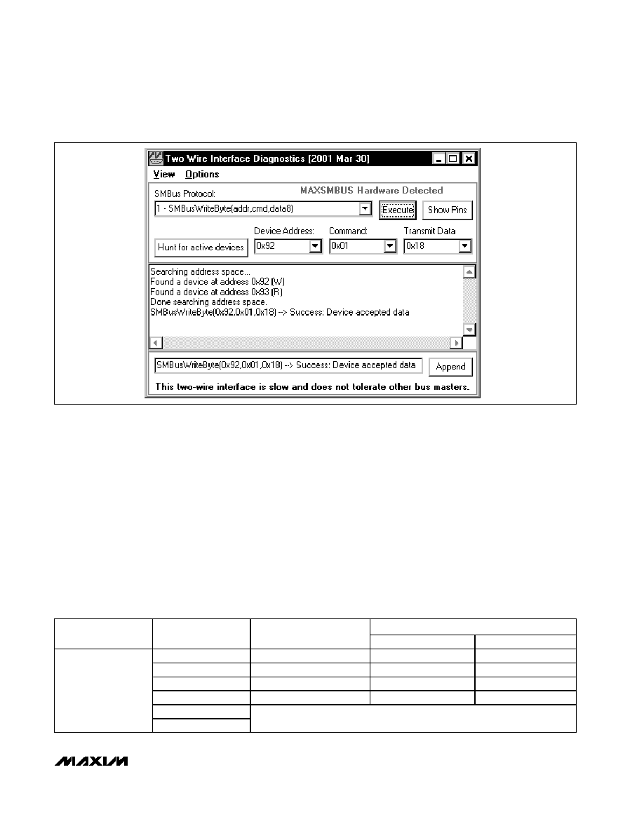
Simple SMBus Commands
There are two methods for communicating with the
MAX9760: through the normal user-interface panel or
through the SMBus commands available by selecting
the 2-Wire Interface Diagnostic item from the Options
pulldown menu. A display pops up that allows the
SMBus protocols, such as Read Byte and Write Byte, to
be executed. To stop normal user-interface execution
so that it does not override the manually set values, turn
off the update timer by unchecking the Automatic
Read checkbox.
The SMBus dialog boxes accept numeric data in binary,
decimal, or hexadecimal. Hexadecimal numbers should
be prefixed by $ or 0x. Binary numbers must be exactly
eight digits. See Figure 3 for an example of this tool.
Note: In places where the slave address asks for an 8-bit
value, it must be the 7-bit slave address of the MAX9760
as determined by ADD with the last bit set to 1 for a read
operation or a zero for a write. Refer to the MAX9760
data sheet for a complete list of registers and functions.
Detailed Description of
Hardware
The MAX9760 EV kit is a stereo, single-supply speak-
er/headphone amplifier. The EV kit is designed to be
driven by any stereo audio source.
The input impedance is 15k
. The EV kit is shipped
with components selected to produce a bass-boosted
frequency response (6dB, f
c
= 100Hz) and a 0dB flat-
frequency response. The EV kit is powered with a 4.5V
to 5.5V supply. A highpass filter is implemented on the
MAX9760 EV kit. The lower 16Hz, -3dB corner frequen-
cy is dependent on components R1, R4, and C1, C4,
C9, and C10.
Multiple input and output jacks facilitate easy connec-
tions to the board. Connect the speakers to terminal
blocks TB1 and TB2. Connect the two stereo input
sources through jacks J1, J2 and J3, J4. Connect the
headphones through jack J5.
MAX9760 Evaluation System/Evaluation Kit
4
_______________________________________________________________________________________
Address Selection
Jumper JU1 sets the MAX9760 slave address. The
default address is 1001 001Y (ADD = VDD). See Table
1 for a complete list of addresses.
Note: The first 7 bits shown are the address. Y (bit 0) is
the SMBus read/write bit. This bit is a 1 for a read oper-
ation or a zero for a write.
Hardware Shutdown Control
Jumper JU5 controls the shutdown function of the
MAX9760 EV kit. Removing the shunt from JU5 allows
the shutdown function to be controlled by an external
signal source connected to the SHDN pad. See Table 2
for shutdown shunt positions.
Manual Headphone Sense Control
To simulate a pair of headphones being inserted into
the headphone jack J5, remove the shunt from jumper
JU6. Connect the load to the LEFT, RIGHT, and GND
pads located by headphone jack J5 (see Table 3 for
jumper settings).
Bass-Boost
The MAX9760 EV kit includes circuitry to increase the
low-frequency (bass) response. To alter the bass
response (see Figure 4), follow the steps below:
1) Choose appropriate gains A
1
and A
2
.
2) Choose the center frequency f
c
.
Evaluates: MAX9760--MAX9763
MAX9760 Evaluation System/Evaluation Kit
_______________________________________________________________________________________
5
Figure 3. The above example shows a simple SMBusWriteByte operation using the included 2-Wire Interface Diagnostics. In this
example, the software is writing data (0x18) to Device Address 0x92, Register Address 0x01. The above data sequence mutes both
output channels of the MAX9760.
Table 1. Shunt Settings for SMBus Address
MAX9760 ADDRESS
JUMPER
SHUNT POSITION
MAX9760 ADDRESS PIN
BINARY
HEXADECIMAL
1≠2*
V
DD
1001 001Y
0x92
3≠4
SDA
1001 010Y
0x94
5≠6
SGND
1001 000Y
0x90
7≠8
SCL
1001 011Y
0x96
9≠10
JU1
11≠12
Not used for the MAX9760 or the MAX9762
(see the Gain Selection Table for more details).
*Default configuration.