 | ÐлекÑÑоннÑй компоненÑ: MAX9770 | СкаÑаÑÑ:  PDF PDF  ZIP ZIP |
Äîêóìåíòàöèÿ è îïèñàíèÿ www.docs.chipfind.ru
General Description
The MAX9770 combines a mono, filterless, Class D
speaker amplifier and stereo DirectDrive headphone
amplifiers in a single device. The MAX9770 operates
from a single 2.5V to 5.5V supply and includes features
that reduce external component count, system cost,
board space, and offer improved audio reproduction.
The speaker amplifier makes use of Maxim's patented
Class D architecture, providing Class AB performance
with Class D efficiency, conserving board space, and
extending battery life. The speaker amplifier delivers
1.2W into an 8
load while offering efficiencies above
85%. A spread-spectrum scheme reduces radiated
emissions caused by the modulation frequency.
Furthermore, the MAX9770 oscillator can be synchro-
nized to an external clock through the SYNC input,
avoiding possible problem frequencies inside a system.
The speaker amplifier features a low 0.025% THD+N,
high 70dB PSRR, and SNR in excess of 90dB.
The headphone amplifiers feature Maxim's patented
DirectDrive architecture that produces a ground-refer-
enced output from a single supply, eliminating the need
for large DC-blocking capacitors. The headphone ampli-
fiers deliver up to 80mW into a 16
load, feature low
0.015% THD+N, high 80dB PSRR, and
±8kV ESD-pro-
tected outputs. A headphone sense input detects the
presence of a headphone, and automatically configures
the amplifiers for either speaker or headphone mode.
The MAX9770 includes internally set, logic-selectable
gain, and a comprehensive input multiplexer/mixer, allow-
ing multiple audio sources to be selected and for true
mono reproduction of a stereo source in speaker mode.
Industry-leading click-and-pop suppression eliminates
audible transients during power and shutdown cycles. A
low-power shutdown mode decreases supply current
consumption to 0.1µA, further extending battery life.
The MAX9770 is offered in space-saving, thermally effi-
cient 28-pin TQFN (5mm x 5mm x 0.8mm) and 28-pin
TSSOP packages. The MAX9770 features thermal-over-
load and output short-circuit protection, and is specified
over the extended -40°C to +85°C temperature range.
Applications
Cellular Phones
PDAs
Compact Notebooks
Features
1.2W Filterless Class D Amplifier Passes FCC
Class B Radiated Emissions Standards with
100mm of Cable
Unique Spread-Spectrum Mode Offers 5dB
Emissions Improvement Over Conventional
Methods
80mW DirectDrive Headphone Amplifier
Eliminates Bulky DC-Blocking Capacitors
High 80dB PSRR at 217Hz
85% Efficiency
Low 0.015% THD+N
Industry-Leading Click-and-Pop Suppression
Integrated 3-Way Input Mixer/Multiplexer
Logic-Selectable Gain
Short-Circuit and Thermal Protection
±
8kV ESD-Protected Headphone Outputs
Low-Power Shutdown Mode
Available in Space-Saving, Thermally Efficient
Packages
28-Pin TQFN (5mm x 5mm x 0.8mm)
28-Pin TSSOP
MAX9770
1.2W Low-EMI, Filterless, Mono Class D Amplifier
with Stereo DirectDrive Headphone Amplifiers
________________________________________________________________ Maxim Integrated Products
1
SPKR
(MONO)
MAX9770
CLASS
D
V
DD
DirectDrive
STEREO
HEADPHONE
L1IN
L2IN
R1IN
R2IN
MONO
GAIN SEL
INPUT SEL
MUTE
SHDN
HPS
PART
TEMP RANGE
PIN-PACKAGE
MAX9770ETI
-40
o
C to +85
o
C
28 TQFN-EP*
MAX9770EUI
-40
o
C to +85
o
C
28 TSSOP
Ordering Information
Simplified Block Diagram
19-3134; Rev 0; 5/04
For pricing, delivery, and ordering information, please contact Maxim/Dallas Direct! at
1-888-629-4642, or visit Maxim's website at www.maxim-ic.com.
Pin Configuration appears at end of data sheet.
Lead-free package.
*EP = Exposed paddle.
MAX9770
1.2W Low-EMI, Filterless, Mono Class D Amplifier
with Stereo DirectDrive Headphone Amplifiers
2
_______________________________________________________________________________________
ABSOLUTE MAXIMUM RATINGS
ELECTRICAL CHARACTERISTICS
(V
DD
= PV
DD
= CPV
DD
= 3.3V, GND = PGND = CPGND = 0V,
SHDN = 3.3V, C1 = C2 = 1µF, C
BIAS
= 0.047µF, SYNC = GND, R
L
=
,
speaker load connected between OUT+ and OUT-, headphone load connected between HPOUT_ and GND, T
A
= T
MIN
to T
MAX
,
unless otherwise noted. Typical values are at T
A
= +25°C.) (Notes 1, 2)
Stresses beyond those listed under "Absolute Maximum Ratings" may cause permanent damage to the device. These are stress ratings only, and functional
operation of the device at these or any other conditions beyond those indicated in the operational sections of the specifications is not implied. Exposure to
absolute maximum rating conditions for extended periods may affect device reliability.
GND to PGND to CPGND......................................-0.3V to +0.3V
V
DD
to PV
DD
to CPV
DD
..........................................-0.3V to +0.3V
V
DD
to GND..............................................................................6V
PV
DD
to PGND .........................................................................6V
CPV
DD
to CPGND ....................................................................6V
CPV
SS
to CPGND....................................................................-6V
SV
SS
to GND ...........................................................................-6V
C1N..........................................(PV
SS
- 0.3V) to (CPGND + 0.3V)
HPOUT_ to GND ....................................................................
±3V
All other pins to GND..................................-0.3V to (V
DD
+ 0.3V)
Continuous Current Into/Out of:
PV
DD
, PGND, OUT_ ......................................................600mA
PV
SS
..............................................................................260mA
Duration of HPOUT_ Short Circuit to V
DD
, PV
DD
,
GND, PGND ...........................................................Continuous
Duration of Short Circuit between
HPOUTL and HPOUTR ..........................................Continuous
Duration of OUT_ Short Circuit to V
DD
, PV
DD
, GND, PGND ..10s
Duration of Short Circuit Between OUT+ and OUT-...............10s
Continuous Power Dissipation (T
A
= +70°C)
28-Pin TQFN (derate 20.8mW/°C above +70°C) .......1667mW
28-Pin TSSOP (derate 12.8mW°C above +70°C) ......1026mW
Junction Temperature ......................................................+150°C
Operating Temperature Range ...........................-40°C to +85°C
Storage Temperature Range .............................-65°C to +150°C
Lead Temperature (soldering, 10s) .................................+300°C
PARAMETER
SYMBOL
CONDITIONS
MIN
TYP
MAX
UNITS
GENERAL
Supply Voltage Range
V
DD
Inferred from PSRR test
2.5
5.5
V
Headphone mode
5.5
10
Quiescent Supply Current
I
DD
No load
Speaker mode
5.2
7.5
mA
Shutdown Supply Current
I
SHDN
SHDN = HPS = GND
0.1
10
µA
Shutdown to Full Operation
t
ON
50
ms
MONO
7
10
Input Impedance
R
IN
(Note 3)
INL_, INR_
14
20
k
Bias Voltage
V
BIAS
1.1
1.25
1.4
V
Feedthrough
From any unselected input to any output,
f = 10kHz
70
dB
SPEAKER AMPLIFIER (GAIN1 = GAIN2 = V
DD
, HPS = GND)
Output Offset Voltage
V
OS
±15
±70
mV
V
DD
= 2.5V to 5.5V
50
70
V
RIPPLE
= 200mV
P-P
, f = 217Hz
70
V
RIPPLE
= 200mV
P-P
, f = 1kHz
68
Power-Supply Rejection Ratio
PSRR
(Note 4)
V
RIPPLE
= 200mV
P-P
, f = 20kHz
50
dB
R
L
= 8
550
V
DD
= 3.3V
R
L
= 4
900
Output Power
P
OUT
f = 1kHz,
THD+N = 1%,
GAIN1 = 1,
GAIN2 = 0
V
DD
= 5V
R
L
= 8
1200
mW
R
L
= 8
, P
OUT
= 300mW, f = 1kHz
0.025
Total Harmonic Distortion Plus
Noise
THD+N
R
L
= 4
, P
OUT
= 300mW, f = 1kHz
0.03
%
MAX9770
1.2W Low-EMI, Filterless, Mono Class D Amplifier
with Stereo DirectDrive Headphone Amplifiers
_______________________________________________________________________________________
3
ELECTRICAL CHARACTERISTICS (continued)
(V
DD
= PV
DD
= CPV
DD
= 3.3V, GND = PGND = CPGND = 0V, SHDN = 3.3V, C1 = C2 = 1µF, C
BIAS
= 0.047µF, SYNC = GND, R
L
=
,
speaker load connected between OUT+ and OUT-, headphone load connected between HPOUT_ and GND, T
A
= T
MIN
to T
MAX
,
unless otherwise noted. Typical values are at T
A
= +25°C.) (Notes 1, 2)
PARAMETER
SYMBOL
CONDITIONS
MIN
TYP
MAX
UNITS
Signal-to-Noise Ratio
SNR
R
L
= 8
, V
OUT
= 2V
RMS
, A-weighted
85.9
dB
SYNC = GND
980
1100
1220
SYNC = FLOAT
1280
1450
1620
Output Switching Frequency
F
S
SYNC = V
DD
1220
±120kHz
kHz
SYNC Frequency Lock Range
800
2000
kHz
Efficiency
P
O
= 1000mW, f = 1kHz
85
%
GAIN1 = 0, GAIN2 = 0
6
GAIN1 = 0, GAIN2 = 1
3
GAIN1 = 1, GAIN2 = 0
9
Gain
A
V
GAIN1 = 1, GAIN2 = 1
0
dB
Gain Accuracy
±5
%
Speaker Path Off-Isolation
HPS = V
DD
, headphone amplifier active,
f = 1kHz
102
dB
HEADPHONE AMPLIFIER (GAIN1 = 1, GAIN2 = 0, HPS = V
DD
)
Output Offset Voltage
V
OS
±5
±10
mV
V
DD
= 2.5V to 5.5V
65
76
V
RIPPLE
= 200mV
P-P
, f = 217kHz
85
V
RIPPLE
= 200mV
P-P
, f = 1kHz
82
Power-Supply Rejection Ratio
PSRR
(Note 3)
V
RIPPLE
= 200mV
P-P
, f = 20kHz
56
dB
R
L
= 32
40
55
V
DD
= 3.3V
R
L
= 16
40
R
L
= 32
60
Output Power
P
OUT
f = 1kHz,
THD+N = 1%
V
DD
= 5V
R
L
= 16
80
mW
R
L
= 32
, P
OUT
= 50mW, f = 1kHz
0.015
Total Harmonic Distortion Plus
Noise
THD+N
R
L
= 16
, P
OUT
= 35mW, f = 1kHz
0.03
%
Signal-to-Noise Ratio
SNR
R
L
= 32
, V
OUT
= 300mV
RMS
,
BW = 22Hz to 22kHz
101
dB
Crosstalk
Between channels, f = 1kHz,
V
IN
= 200mV
P-P
80
dB
Headphone Off-Isolation
HPS = GND, speaker amplifier active,
f = 1kHz
96
dB
10
0.001
10
100
10k
100k
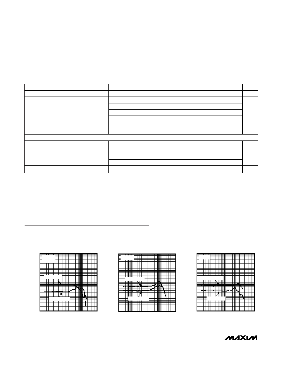
TOTAL HARMONIC DISTORTION PLUS NOISE
vs. FREQUENCY (SPEAKER MODE)
0.01
0.1
1
MAX9770 toc01
FREQUENCY (Hz)
THD+N (%)
1k
V
DD
= +5V
R
L
= 4
P
OUT
= 25mW
P
OUT
= 1000mW
10
0.001
10
100
10k
100k
TOTAL HARMONIC DISTORTION PLUS NOISE
vs. FREQUENCY (SPEAKER MODE)
0.01
0.1
1
MAX9770 toc02
FREQUENCY (Hz)
THD+N (%)
1k
R
L
= 4
P
OUT
= 100mW
P
OUT
= 500mW
10
0.001
10
100
10k
100k
TOTAL HARMONIC DISTORTION PLUS NOISE
vs. FREQUENCY (SPEAKER MODE)
0.01
0.1
1
MAX9770 toc03
FREQUENCY (Hz)
THD+N (%)
1k
R
L
= 8
P
OUT
= 40mW
P
OUT
= 400mW
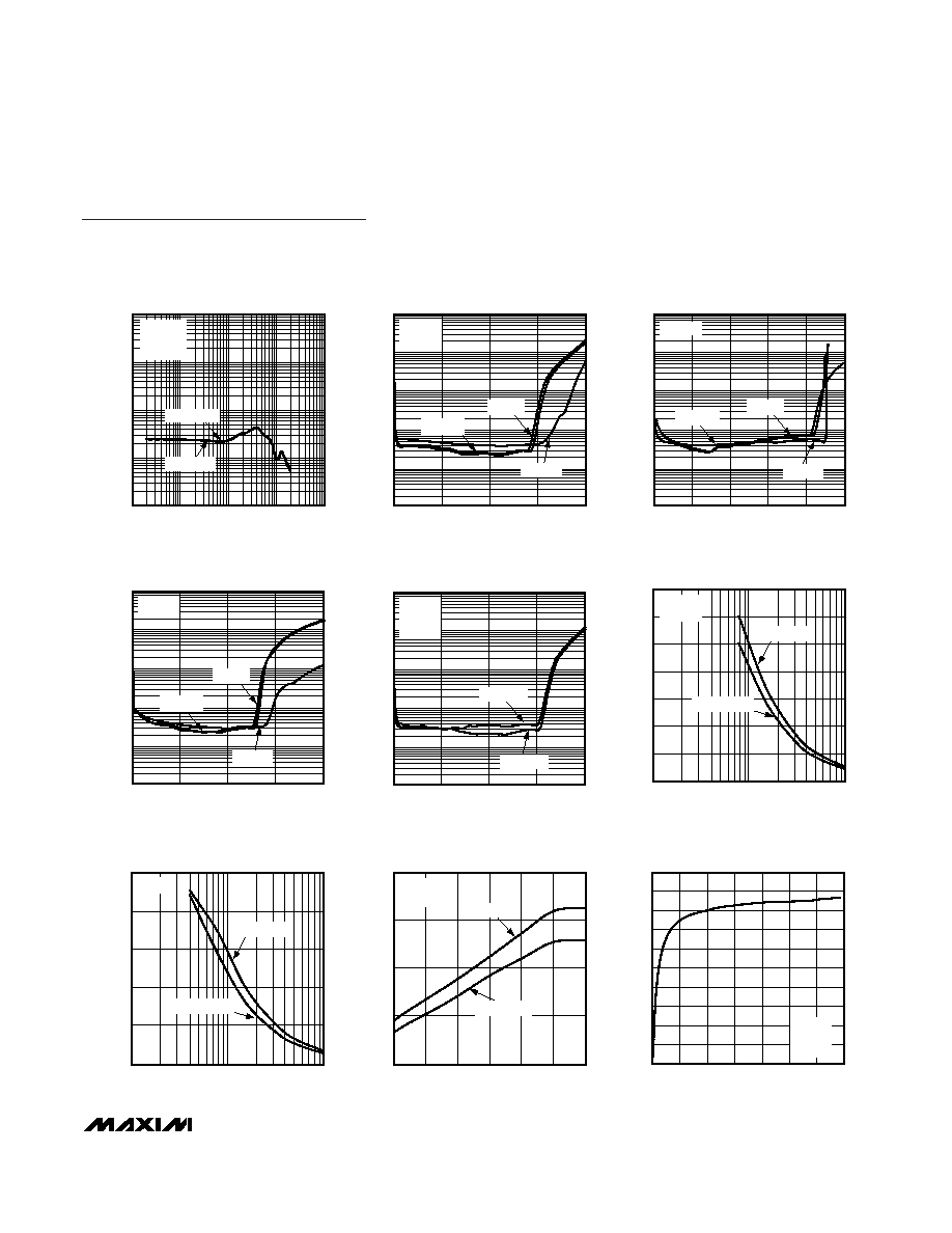
Typical Operating Characteristics
(V
DD
= 3.3V, BW = 22Hz to 22kHz, GAIN1 = 1, GAIN2 = 0, spread-spectrum mode, headphone outputs in phase.)
MAX9770
1.2W Low-EMI, Filterless, Mono Class D Amplifier
with Stereo DirectDrive Headphone Amplifiers
4
_______________________________________________________________________________________
ELECTRICAL CHARACTERISTICS (continued)
(V
DD
= PV
DD
= CPV
DD
= 3.3V, GND = PGND = CPGND = 0V, SHDN = 3.3V, C1 = C2 = 1µF, C
BIAS
= 0.047µF, SYNC = GND, R
L
=
,
speaker load connected between OUT+ and OUT-, headphone load connected between HPOUT_ and GND, T
A
= T
MIN
to T
MAX
,
unless otherwise noted. Typical values are at T
A
= +25°C.) (Notes 1, 2)
PARAMETER
SYMBOL
CONDITIONS
MIN
TYP
MAX
UNITS
Capacitive-Load Drive
C
L
1000
pF
GAIN1 = 0, GAIN2 = 0
7
GAIN1 = 0, GAIN2 = 1
4
GAIN1 = 1, GAIN2 = 0
-2
Gain
A
V
GAIN1 = 1, GAIN2 = 1
1
dB
Gain Accuracy
±2.5
%
ESD Protection
HPOUTR, HPOUTL, IEC Air Discharge
±8
kV
DIGITAL INPUTS (
SHDN
, SYNC, HPS, GAIN_, SEL_)
Input Voltage High
V
IH
2
V
Input Voltage Low
V
IL
0.8
V
SYNC input
±25
Input Leakage Current
All other logic inputs
±1
µA
HPS Input Current
HPS = GND
-10
µA
Note 1:
All devices are 100% production tested at +25°C. All temperature limits are guaranteed by design.
Note 2:
Speaker amplifier testing performed with a resistive load in series with an inductor to simulate an actual speaker load. For
R
L
= 4
, L = 47µH. For R
L
= 8
, L = 68µH.
Note 3:
Guaranteed by design, not production tested.
Note 4:
PSRR is specified with the amplifier inputs connected to GND through C
IN
.
MAX9770
1.2W Low-EMI, Filterless, Mono Class D Amplifier
with Stereo DirectDrive Headphone Amplifiers
_______________________________________________________________________________________
5
10
0.001
10
100
10k
100k
TOTAL HARMONIC DISTORTION PLUS NOISE
vs. FREQUENCY (SPEAKER MODE)
0.01
0.1
1
MAX9770 toc04
FREQUENCY (Hz)
THD+N (%)
1k
V
DD
= 5V
P
OUT
= 1W
R
L
= 8
SSM MODE
FFM MODE
100
0
400
800
1200
1600
10
1
0.1
0.01
0.001
TOTAL HARMONIC DISTORTION PLUS NOISE
vs. OUTPUT POWER (SPEAKER MODE)
MAX9770 toc05
OUTPUT POWER (mW)
THD+N (%)
V
DD
= 5V
R
L
= 8
f = 20Hz
f = 1kHz
f = 10kHz
100
0
200
600
400
800
1000
10
1
0.1
0.01
0.001
TOTAL HARMONIC DISTORTION PLUS NOISE
vs. OUTPUT POWER (SPEAKER MODE)
MAX9770 toc06
OUTPUT POWER (mW)
THD+N (%)
f = 20Hz
f = 1kHz
f = 10kHz
R
L
= 4
100
0
200
400
600
800
10
1
0.1
0.01
0.001
TOTAL HARMONIC DISTORTION PLUS NOISE
vs. OUTPUT POWER (SPEAKER MODE)
MAX9770 toc07
OUTPUT POWER (mW)
THD+N (%)
R
L
= 8
f = 20Hz
f = 1kHz
f = 10kHz
100
0
400
800
1200
1600
10
1
0.1
0.01
0.001
TOTAL HARMONIC DISTORTION PLUS NOISE
vs. OUTPUT POWER (SPEAKER MODE)
MAX9770 toc08
OUTPUT POWER (mW)
THD+N (%)
V
DD
= 5V
f = 1kHz
R
L
= 8
SSM MODE
FFM MODE
1.75
0
1
10
100
OUTPUT POWER
vs. LOAD RESISTANCE (SPEAKER MODE)
0.50
0.25
MAX9770 toc09
LOAD RESISTANCE (
)
OUTPUT POWER (W)
0.75
1.00
1.25
1.50
V
DD
= 5V
f = 1kHz
THD+N = 10%
THD+N = 1%
1.0
0
1
10
100
OUTPUT POWER
vs. LOAD RESISTANCE (SPEAKER MODE)
0.2
MAX9770 toc10
LOAD RESISTANCE (
)
OUTPUT POWER (W)
0.4
0.6
0.8
f = 1kHz
THD+N = 10%
THD+N = 1%
2.0
1.5
1.0
0.5
0
2.5
4.0
3.0
3.5
4.5
5.0
5.5
OUTPUT POWER
vs. SUPPLY VOLTAGE (SPEAKER MODE)
MAX9770 toc11
SUPPLY VOLTAGE (V)
OUTPUT POWER (W)
f = 1kHz
R
L
= 8
THD+N = 10%
THD+N = 1%
0
30
20
10
50
40
90
80
70
60
100
0
0.2
0.4
0.6
0.8
1.0
1.2
1.4
EFFICIENCY vs. OUTPUT POWER
MAX9770 toc12
OUTPUT POWER (W)
EFFICIENCY (%)
V
DD
= 5V
f = 1kHz
R
L
= 8
Typical Operating Characteristics (continued)
(V
DD
= 3.3V, BW = 22Hz to 22kHz, GAIN1 = 1, GAIN2 = 0, spread-spectrum mode, headphone outputs in phase.)