 | –≠–ª–µ–∫—Ç—Ä–æ–Ω–Ω—ã–π –∫–æ–º–ø–æ–Ω–µ–Ω—Ç: MAX9778 | –°–∫–∞—á–∞—Ç—å:  PDF PDF  ZIP ZIP |
General Description
The MAX9777/MAX9778 combine a stereo 3W bridge-
tied load (BTL) audio power amplifier, stereo single-
ended (SE) headphone amplifier, headphone sensing,
and a 2:1 input multiplexer all in a tiny 28-pin thin QFN
package. These devices operate from a single 4.5V to
5.5V supply and feature an industry-leading 100dB
PSRR, allowing these devices to operate from noisy
supplies without the addition of a linear regulator. An
ultra-low 0.002% THD+N ensures clean, low-distortion
amplification of the audio signal. Patented click-and-
pop suppression minimizes audible transients on power
and shutdown cycles. Power-saving features include
low 4mV V
OS
(minimizes DC current drain through the
speakers), low 13mA supply current, and a 10µA shut-
down mode. A MUTE function allows the outputs to be
quickly enabled or disabled.
A headphone sense input detects the presence of a
headphone jack and automatically configures the
amplifiers for either speaker or headphone mode. In
speaker mode, the amplifiers can deliver up to 3W of
continuous average power into a 3 load. In head-
phone mode, the amplifier can deliver up to 200mW of
continuous average power into a 16 load. The gain of
the amplifiers is externally set, allowing maximum flexi-
bility in optimizing output levels for a given load. The
amplifiers also feature a 2:1 input multiplexer, allowing
multiple audio sources to be selected. The multiplexer
can also be used to compensate for limitations in the
frequency response of the loud speakers by selecting
an external equalizer network. The various functions are
controlled by either an I
2
C
-compatible (MAX9777) or
simple parallel control interface (MAX9778).
The MAX9777/MAX9778 are available in a thermally
efficient 28-pin thin QFN package (5mm x 5mm x
0.8mm). These devices have thermal-overload protec-
tion (OVP) and are specified over the extended -40∞C
to +85∞C temperature range.
Features
o Industry-Leading, Ultra-High 100dB PSRR
o PC99/01 Compliant
o 3W BTL Stereo Speaker Amplifier
o 200mW Stereo Headphone Amplifier
o Low 0.002% THD+N
o Patented Click-and-Pop Suppression
o ESD-Protected Outputs
o Low Quiescent Current: 13mA
o Low-Power Shutdown Mode: 10µA
o MUTE Function
o Headphone Sense Input
o Stereo 2:1 Input Multiplexer
o Optional 2-Wire, I
2
C-Compatible or Parallel
Interface
o Tiny 28-Pin Thin QFN (5mm
x
5mm
x
0.8mm)
Package
MAX9777/MAX9778
Stereo 3W Audio Power Amplifiers with
Headphone Drive and Input Mux
________________________________________________________________
Maxim Integrated Products
1
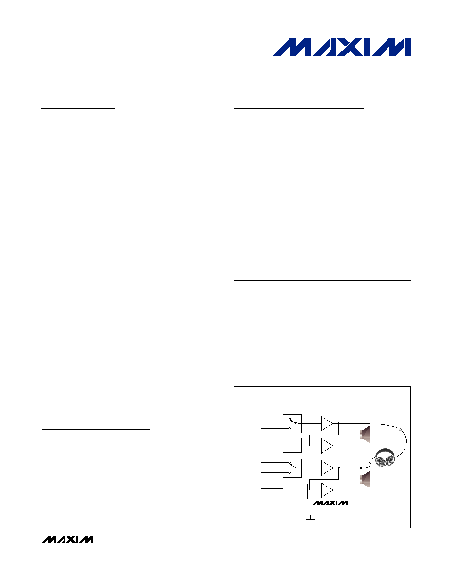
SE/
BTL
SINGLE SUPPLY
4.5V TO 5.5V
I
2
C-
COMPATIBLE
MAX9777
LEFT IN
1
LEFT IN
2
RIGHT IN
1
RIGHT IN
2
CONTROL
Simplified Block Diagram
Ordering Information
19-0509; Rev 0; 4/06
For pricing, delivery, and ordering information, please contact Maxim/Dallas Direct! at
1-888-629-4642, or visit Maxim's website at www.maxim-ic.com.
PART
CONTROL
INTERFACE
PIN-
PACKAGE
PK G
C O D E
MAX9777ETI+
I
2
C Compatible
28 Thi n QFN - E P * T2855-6
MAX9778ETI+
Parallel
28 Thi n QFN - E P * T2855-6
Pin Configurations and Functional Diagrams appear at end
of data sheet.
Note: All devices are specified over the -40∞C to +85∞C operat-
ing temperature range.
+Denotes lead-free package.
*EP = Exposed paddle.
Purchase of I
2
C components from Maxim Integrated Products,
Inc., or one of its sublicensed Associate Companies, conveys a
license under the Philips I
2
C Patent Rights to use these compo-
nents in an I
2
C system, provided that the system conforms to the
I
2
C Standard Specification defined by Philips.
Notebooks
Portable DVD Players
Tablet PCs
PC Audio Peripherals
Camcorders
Multimedia Monitor
Applications
MAX9777/MAX9778
Stereo 3W Audio Power Amplifiers with
Headphone Drive and Input Mux
2
_______________________________________________________________________________________
ABSOLUTE MAXIMUM RATINGS
Stresses beyond those listed under "Absolute Maximum Ratings" may cause permanent damage to the device. These are stress ratings only, and functional
operation of the device at these or any other conditions beyond those indicated in the operational sections of the specifications is not implied. Exposure to
absolute maximum rating conditions for extended periods may affect device reliability.
V
DD
to GND ...........................................................................+6V
PV
DD
to V
DD
.......................................................................±0.3V
PGND to GND.....................................................................±0.3V
All Other Pins to GND.................................-0.3V to (V
DD
+ 0.3V)
Continuous Input Current (into any pin except power-supply
and output pins) ...............................................................±20mA
OUT__ Short Circuit to GND, V
DD
..........................................10s
Short Circuit Between OUT_+ and OUT_- .................Continuous
Continuous Power Dissipation (T
A
= +70∞C)
28-Pin TQFN, Multilayer Board
(derate 34.5mW/∞C above +70∞C) ..........................2758.6mW
Operating Temperature Range ...........................-40∞C to +85∞C
Storage Temperature Range .............................-65∞C to +150∞C
Junction Temperature ......................................................+150∞C
Lead Temperature (soldering, 10s) .................................+300∞C
ELECTRICAL CHARACTERISTICS
(V
DD
= PV
DD
= 5.0V, GND = PGND = 0V, V
SHDN
= 5V, C
BIAS
= 1µF, R
IN
= R
F
= 15k, R
L
= . T
A
= T
MIN
to T
MAX
, unless otherwise
noted. Typical values are at T
A
= +25∞C.) (Note 1)
PARAMETER
SYMBOL
CONDITIONS
MIN
TYP
MAX
UNITS
Supply Voltage Range
V
DD
/PV
DD
Inferred from PSRR test
4.5
5.5
V
BTL mode, HPS = 0V, MAX9777/MAX9778
13
32
Quiescent Supply Current
(I
VDD
+ I
PVDD
)
I
DD
Single-ended mode, HPS = V
DD
7
18
mA
Shutdown Current
I
SHDN
SHDN = GND
10
50
µA
Switching Time
t
SW
Gain or input switching
10
µs
C
BIAS
= 1µF
300
Turn-On Time
t
ON
C
BIAS
= 0.1µF
30
ms
Thermal Shutdown Threshold
+160
o
C
Thermal Shutdown Hysteresis
15
o
C
OUTPUT AMPLIFIERS (SPEAKER MODE, HPS = GND)
Output Offset Voltage
V
OS
OUT_+ - OUT_-, A
V
= 1V/V
±4
±32
mV
V
DD
= 4.5V to 5.5V
75
100
f = 1kHz, V
RIPPLE
= 200mV
P-P
82
Power-Supply Rejection Ratio
(Note 2)
PSRR
f = 20kHz, V
RIPPLE
= 200mV
P-P
70
dB
R
L
= 8
1.4
R
L
= 4
2.6
Output Power
P
OUT
f
IN
= 1kHz,
THD+N < 1%,
T
A
= +25∞C
R
L
= 3
3
W
P
OUT
= 1W, R
L
= 8
0.005
Total Harmonic Distortion Plus
Noise
THD+N
f
IN
= 1kHz, BW =
22Hz to 22kHz
P
OUT
= 2W, R
L
= 4
0.01
%
Signal-to-Noise Ratio
SNR
R
L
= 8
, P
OUT
= 1W, BW = 22Hz to 22kHz
95
dB
Slew Rate
SR
1.6
V/µs
Maximum Capacitive Load Drive
C
L
No sustained oscillations
1
nF
Crosstalk
f
IN
= 10kHz
73
dB
Into shutdown
-50
Click/Pop Level
K
CP
Peak voltage, A-weighted,
32 samples per second
(Notes 2, 6)
Out of shutdown
-65
dBV
MAX9777/MAX9778
Stereo 3W Audio Power Amplifiers with
Headphone Drive and Input Mux
_______________________________________________________________________________________
3
ELECTRICAL CHARACTERISTICS (continued)
(V
DD
= PV
DD
= 5.0V, GND = PGND = 0V, V
SHDN
= 5V, C
BIAS
= 1µF, R
IN
= R
F
= 15k, R
L
= . T
A
= T
MIN
to T
MAX
, unless otherwise
noted. Typical values are at T
A
= +25∞C.) (Note 1)
PARAMETER
SYMBOL
CONDITIONS
MIN
TYP
MAX
UNITS
OUTPUT AMPLIFIERS (HEADPHONE MODE, HPS = V
DD
)
V
DD
= 4.5V to 5.5V
75
106
f = 1kHz, V
RIPPLE
= 200mV
P-P
88
Power-Supply Rejection Ratio
(Note 2)
PSRR
f = 20kHz, V
RIPPLE
= 200mV
P-P
76
dB
R
L
= 32
88
Output Power
P
OUT
f
IN
= 1kHz, THD+N <
1%, T
A
= +25∞C
R
L
= 16
200
mW
P
OUT
= 60mW,
R
L
= 32
0.002
Total Harmonic Distortion Plus
Noise
THD+N
f
IN
= 1kHz,
BW = 22Hz to 22kHz
P
OUT
= 125mW,
R
L
= 16
0.002
%
Signal-to-Noise Ratio
SNR
R
L
= 32
, BW = 22Hz to 22kHz,
V
OUT
= 1V
RMS
92
dB
Slew Rate
SR
1.8
V/µs
Maximum Capacitive Load Drive
C
L
No sustained oscillations
2
nF
Crosstalk
f
IN
= 10kHz
78
dB
BIAS VOLTAGE (BIAS)
BIAS Voltage
V
BIAS
2.35
2.5
2.65
V
Output Resistance
R
BIAS
50
k
DIGITAL INPUTS (MUTE,
SHDN, HPS_EN, GAINA/B, IN1111/2)
Input-Voltage High
V
IH
2
V
Input-Voltage Low
V
IL
0.8
V
Input Leakage Current
I
IN
±1
µA
HEADPHONE SENSE INPUT (HPS)
Input-Voltage High
V
IH
0.9 x
V
DD
V
Input-Voltage Low
V
IL
0.7 x
V
DD
V
Input Leakage Current
I
IN
±1
µA
Into shutdown
-70
Click/Pop Level
K
CP
Peak voltage, A-weighted,
32 samples per second
(Notes 2, 4)
Out of shutdown
-52
dBV

MAX9777/MAX9778
Stereo 3W Audio Power Amplifiers with
Headphone Drive and Input Mux
4
_______________________________________________________________________________________
ELECTRICAL CHARACTERISTICS (continued)
(V
DD
= PV
DD
= 5.0V, GND = PGND = 0V, V
SHDN
= 5V, C
BIAS
= 1µF, R
IN
= R
F
= 15k, R
L
= . T
A
= T
MIN
to T
MAX
, unless otherwise
noted. Typical values are at T
A
= +25∞C.) (Note 1)
PARAMETER
SYMBOL
CONDITIONS
MIN
TYP
MAX
UNITS
2-WIRE SERIAL INTERFACE (SCL, SDA, ADD,
INT) (MAX9777)
Input-Voltage High
V
IH
2.6
V
Input-Voltage Low
V
IL
0.8
V
Input Hysteresis
0.2
V
Input High Leakage Current
I
IH
V
IN
= 5V
±1
µA
Input Low Leakage Current
I
IL
V
IN
= 0V
±1
µA
Input Capacitance
C
IN
10
pF
Output-Voltage Low
V
OL
I
OL
= 3mA
0.4
V
Output Current High
I
OH
V
OH
= 5V
1
µA
TIMING CHARACTERISTICS (MAX9777)
Serial Clock Frequency
f
SCL
400
kHz
Bus Free Time Between STOP
and START Conditions
t
BUF
1.3
µs
START Condition Hold Time
t
HD:STA
0.6
µs
START Condition Setup Time
t
SU:STA
0.6
µs
Clock Period Low
t
LOW
1.3
µs
Clock Period High
t
HIGH
0.6
µs
Data Setup Time
t
SU:DAT
100
ns
Data Hold Time
t
HD:DAT
(Note 3)
0
0.9
µs
Receive SCL/SDA Rise Time
t
r
(Note 4)
20 +
0.1C
B
300
ns
Receive SCL/SDA Fall Time
t
f
(Note 4)
20 +
0.1C
B
300
ns
Transmit SDA Fall Time
t
f
(Note 4)
20 +
0.1C
B
250
ns
Pulse Width of Suppressed
Spike
t
SP
(Note 5)
50
ns
Note 1: All devices are 100% production tested at +25∞C. All temperature limits are guaranteed by design.
Note 2: Inputs AC-coupled to GND.
Note 3: A master device must provide a hold time of at least 300ns for the SDA signal to bridge the undefined region of SCL's
falling edge.
Note 4: C
B
= total capacitance of one of the bus lines in picofarads. Device tested with C
B
= 400pF. 1k pullup resistors connected
from SDA/SCL to V
DD
.
Note 5: Input filters on SDA, SCL, and ADD suppress noise spikes of less than 50ns.
Note 6: Headphone mode testing performed with 32 resistive load connected to GND. Speaker mode testing performed with 8
resistive load connected to GND. Mode transitions are controlled by
SHDN. KCP level is calculated as 20log[(peak voltage
during mode transition, no input signal)/1V
RMS
]. Units are expressed in dBV.
MAX9777/MAX9778
Stereo 3W Audio Power Amplifiers with
Headphone Drive and Input Mux
_______________________________________________________________________________________
5
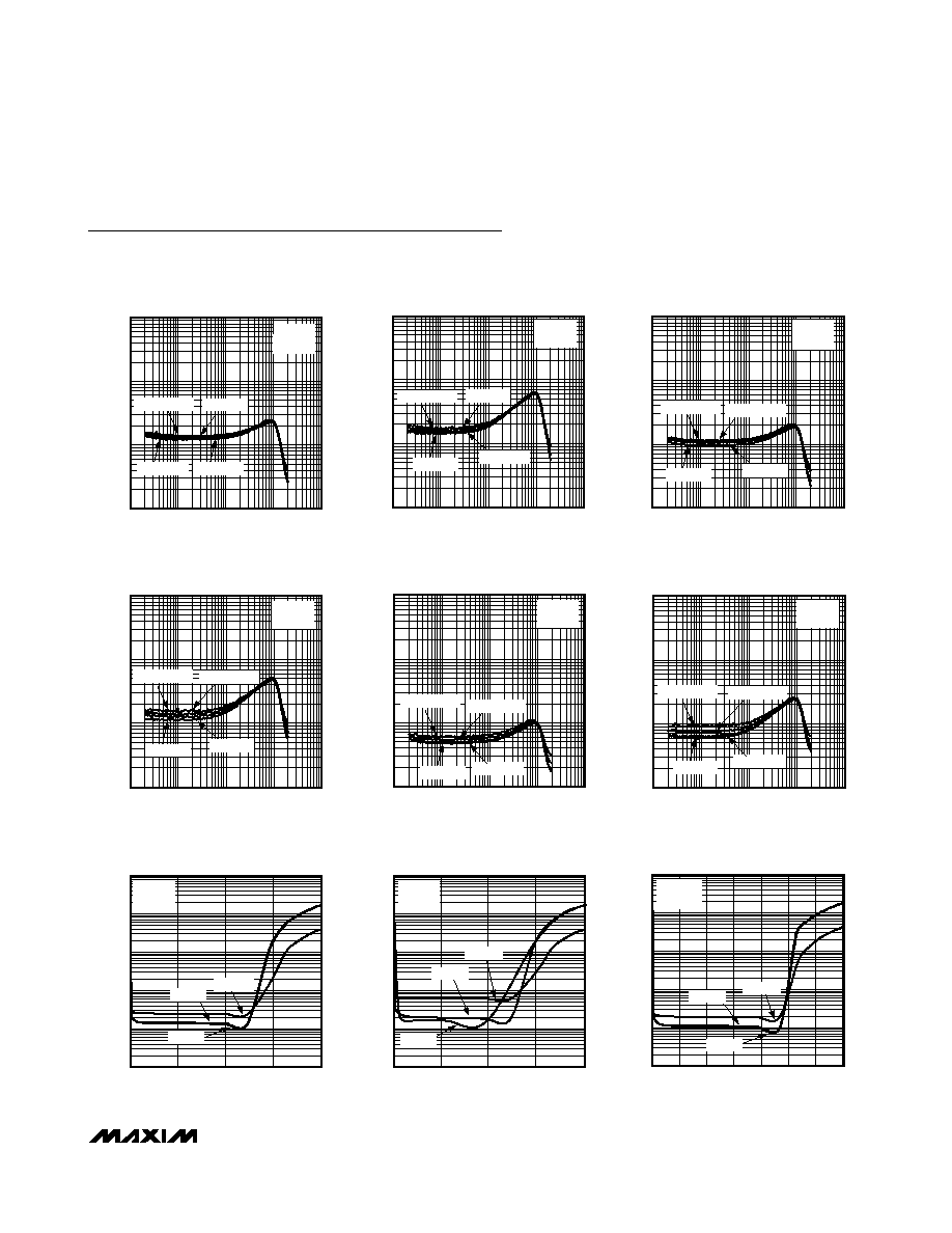
TOTAL HARMONIC DISTORTION PLUS NOISE
vs. FREQUENCY (SPEAKER MODE)
MAX9777/78 toc01
FREQUENCY (Hz)
THD+N (%)
10k
1k
100
0.01
0.1
1
0.001
10
100k
R
L
= 3
A
V
= 2V/V
P
OUT
= 2.5W
P
OUT
= 2W
P
OUT
= 500mW
P
OUT
= 1W
TOTAL HARMONIC DISTORTION PLUS NOISE
vs. FREQUENCY (SPEAKER MODE)
MAX9777/78 toc02
FREQUENCY (Hz)
THD+N (%)
10k
1k
100
0.01
0.1
1
0.001
10
100k
R
L
= 3
A
V
= 4V/V
P
OUT
= 2.5W
P
OUT
= 2W
P
OUT
= 500mW
P
OUT
= 1W
TOTAL HARMONIC DISTORTION PLUS NOISE
vs. FREQUENCY (SPEAKER MODE)
MAX9777/78 toc03
FREQUENCY (Hz)
THD+N (%)
10k
1k
100
0.01
0.1
1
0.001
10
100k
R
L
= 4
A
V
= 2V/V
P
OUT
= 2W
P
OUT
= 1W
P
OUT
= 500mW
P
OUT
= 250mW
TOTAL HARMONIC DISTORTION PLUS NOISE
vs. FREQUENCY (SPEAKER MODE)
MAX9777/78 toc04
FREQUENCY (Hz)
THD+N (%)
10k
1k
100
0.01
0.1
1
0.001
10
100k
R
L
= 4
A
V
= 4V/V
P
OUT
= 250mW
P
OUT
= 2W
P
OUT
= 1W
P
OUT
= 500mW
TOTAL HARMONIC DISTORTION PLUS NOISE
vs. FREQUENCY (SPEAKER MODE)
MAX9777/78 toc05
FREQUENCY (Hz)
THD+N (%)
10k
1k
100
0.01
0.1
1
0.001
10
100k
R
L
= 8
A
V
= 2V/V
P
OUT
= 250mW
P
OUT
= 1.2W
P
OUT
= 1W
P
OUT
= 500mW
TOTAL HARMONIC DISTORTION PLUS NOISE
vs. FREQUENCY (SPEAKER MODE)
MAX9777/78 toc06
FREQUENCY (Hz)
THD+N (%)
10k
1k
100
0.01
0.1
1
0.001
10
100k
P
OUT
= 250mW
P
OUT
= 1.2W
P
OUT
= 1W
P
OUT
= 500mW
R
L
= 8
A
V
= 4V/V
TOTAL HARMONIC DISTORTION PLUS NOISE
vs. OUTPUT POWER (SPEAKER MODE)
MAX9777/78 toc07
OUTPUT POWER (W)
THD+N (%)
3
2
1
0.01
10
1
0.1
100
0.001
0
4
A
V
= 2V/V
R
L
= 3
f = 1kHz
f = 20Hz
f = 10kHz
TOTAL HARMONIC DISTORTION PLUS NOISE
vs. OUTPUT POWER (SPEAKER MODE)
MAX9777/78 toc08
OUTPUT POWER (W)
THD+N (%)
3
2
1
0.01
10
1
0.1
100
0.001
0
4
A
V
= 4V/V
R
L
= 3
f = 20Hz
f = 1kHz
f = 10kHz
TOTAL HARMONIC DISTORTION PLUS NOISE
vs. OUTPUT POWER (SPEAKER MODE)
MAX9777/78 toc09
OUTPUT POWER (W)
THD+N (%)
2.5
3.0
2.0
1.5
1.0
0.5
0.01
10
1
0.1
100
0.001
0
3.5
A
V
= 2V/V
R
L
= 4
f = 20Hz
f = 1kHz
f = 10kHz
Typical Operating Characteristics
(V
DD
= PV
DD
= 5V, GND = PGND = 0V, V
SHDN
= 5V, C
BIAS
= 1µF, T
A
= +25∞C, unless otherwise noted.)