 | –≠–ª–µ–∫—Ç—Ä–æ–Ω–Ω—ã–π –∫–æ–º–ø–æ–Ω–µ–Ω—Ç: MAX9787 | –°–∫–∞—á–∞—Ç—å:  PDF PDF  ZIP ZIP |
General Description
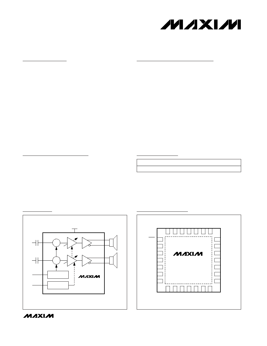
The MAX9787 combines a stereo, 2.2W audio power
amplifier with an analog volume control in a single device.
A high 90dB PSRR and low 0.01% THD+N ensures clean,
low-distortion amplification of the audio signal.
The analog volume control can be driven with a poten-
tiometer, an RC-filtered PWM source, or a DAC output.
A BEEP input allows the addition of alert signals from
the controller to the audio path.
Industry-leading, click-and-pop suppression eliminates
audible transients during power and shutdown cycles.
Other features include single-supply voltage, a shut-
down mode, logic-selectable gain, thermal-overload,
and output short-circuit protection.
The MAX9787 is offered in a space-saving, thermally
efficient, 28-pin, thin QFN (5mm x 5mm x 0.8mm) pack-
age, and is specified over the extended -40∞C to +85∞C
temperature range.
Applications
Notebook PCs
Flat-Panel TVs
Tablet PCs
PC Displays
Features
Class AB, 2.2W, Stereo BTL Speaker Amplifiers
Analog Volume Control
BEEP Input with Glitch Filter
5V Single-Supply Operation
High 90dB PSRR
Low-Power Shutdown Mode
Industry-Leading Click-and-Pop Suppression
Low 0.01% THD+N at 1kHz
Short-Circuit and Thermal Protection
Selectable-Gain Settings
Space-Saving 28-Pin TQFN (5mm x 5mm x 0.8mm)
MAX9787
2.2W Stereo Audio Power Amplifier
with Analog Volume Control
________________________________________________________________ Maxim Integrated Products
1
Ordering Information
19-3882; Rev 0; 10/05
For pricing, delivery, and ordering information, please contact Maxim/Dallas Direct! at
1-888-629-4642, or visit Maxim's website at www.maxim-ic.com.
PART
PIN-PACKAGE
PKG CODE
MAX9787ETI+
28 TQFN-EP*
T2855N-1
Note: This device is specified for -40∞C to +85∞C operation.
+Denotes lead-free package.
*EP = Exposed paddle.
+5V
VOLUME
BEEP
MAX9787
Typical Operating Circuit
BIAS
GND
PGND
OUTR+
OUTR-
PV
DD
PV
DD
1
2
+
3
4
5
6
7
21
20
19
18
17
16
15
INL
BEEP
PGND
OUTL+
OUTL-
PV
DD
CPV
DD
8
9
10
11
12
13
14
C1P
CPGND
C1N
CPV
SS
V
SS
N.C.
N.C.
28
27
26
25
24
23
22
VOL
INR
GND
V
DD
GAIN1
GAIN2
SHDN
MAX9787
THIN QFN
TOP VIEW
*EP
*EXPOSED PAD.
Pin Configuration
Portable DVD Players
LCD Projectors
Multimedia Monitors
MAX9787
2.2W Stereo Audio Power Amplifier
with Analog Volume Control
2
_______________________________________________________________________________________
ABSOLUTE MAXIMUM RATINGS
Stresses beyond those listed under "Absolute Maximum Ratings" may cause permanent damage to the device. These are stress ratings only, and functional
operation of the device at these or any other conditions beyond those indicated in the operational sections of the specifications is not implied. Exposure to
absolute maximum rating conditions for extended periods may affect device reliability.
Supply Voltage (V
DD
, PV
DD
, CPV
DD
to GND) .......................+6V
GND to PGND.....................................................................±0.3V
CPV
SS
, C1N, V
SS
to GND .........................-6.0V to (GND + 0.3V)
Any Other Pin .............................................-0.3V to (V
DD
+ 0.3V)
Duration of OUT_ Short Circuit to GND or PV
DD
........Continuous
Duration of OUT_+ Short Circuit to OUT_- .................Continuous
Continuous Current (PV
DD
, OUT_, PGND) ...........................1.7A
Continuous Current (CPV
DD
, C1N, C1P, CPV
SS,
V
SS
)......850mA
Continuous Input Current (all other pins) .........................±20mA
Continuous Power Dissipation (T
A
= +70∞C)
28-Pin Thin QFN (derate 23.8mW/∞C above +70∞C) .......1.9W
Junction Temperature ......................................................+150∞C
Operating Temperature Range ...........................-40∞C to +85∞C
Storage Temperature Range .............................-65∞C to +150∞C
Lead Temperature (soldering, 10s) .................................+300∞C
ELECTRICAL CHARACTERISTICS
(V
DD
= PV
DD
= CPV
DD
= 5V, GND = PGND = CPGND = 0V,
SHDN = V
DD
, C
BIAS
= 1µF, C1 = C2 = 1µF, speaker load
terminated between OUT_+ and OUT_-, GAIN1 = GAIN2 = VOL = 0V, T
A
= T
MIN
to T
MAX
, unless otherwise noted. Typical values are
at T
A
= +25∞C.) (Note 1)
PARAMETER
SYMBOL
CONDITIONS
MIN
TYP
MAX
UNITS
GENERAL
Supply Voltage Range
V
DD
, PV
DD
Inferred from PSRR test
4.5
5.5
V
Quiescent Supply Current
I
DD
14
29
mA
Shutdown Supply Current
I
SHDN
SHDN = GND
0.2
5
µA
Bias Voltage
V
BIAS
1.7
1.8
1.9
V
Switching Time
t
SW
Gain or input switching
10
µs
Input Resistance
R
IN
Amplifier inputs (Note 2)
10
20
30
k
Turn-On Time
t
SON
25
ms
Output Offset Voltage
V
OS
Measured between OUT_+ and OUT_-,
T
A
= +25∞C
±0.4
±6
mV
PV
DD
or V
DD
= 4.5V to 5.5V (T
A
= +25∞C)
75
90
f = 1kHz, V
RIPPLE
= 200mV
P-P
80
Power-Supply Rejection Ratio
(Note 3)
PSRR
f = 10kHz, V
RIPPLE
= 200mV
P-P
55
dB
R
L
= 8
0.65
0.8
R
L
= 4
1.2
1.5
Output Power (Note 4)
P
OUT
THD+N = 1%,
f = 1kHz,
T
A
= +25∞C
R
L
= 3
2.2
W
R
L
= 8
, P
OUT
= 500mW, f = 1kHz
0.01
Total Harmonic Distortion Plus
Noise
THD+N
R
L
= 4
, P
OUT
= 1W, f = 1kHz
0.02
%

MAX9787
2.2W Stereo Audio Power Amplifier
with Analog Volume Control
_______________________________________________________________________________________
3
ELECTRICAL CHARACTERISTICS (continued)
(V
DD
= PV
DD
= CPV
DD
= 5V, GND = PGND = CPGND = 0V, SHDN = V
DD
, C
BIAS
= 1µF, C1 = C2 = 1µF, speaker load
terminated between OUT_+ and OUT_-, GAIN1 = GAIN2 = VOL = 0V, T
A
= T
MIN
to T
MAX
, unless otherwise noted. Typical values are
at T
A
= +25∞C.) (Note 1)
PARAMETER
SYMBOL
CONDITIONS
MIN
TYP
MAX
UNITS
Signal-to-Noise Ratio
SNR
R
L
= 8
, P
OUT
= 500mW, BW = 22Hz to
22kHz
90
dB
Noise
V
n
BW = 22Hz to 22kHz, A-weighted
80
µV
RMS
Capacitive-Load Drive
C
L
No sustained oscillations
200
pF
Crosstalk
L to R, R to L, f = 10kHz
75
dB
Slew Rate
SR
1.4
V/µs
GAIN1 = 0, GAIN2 = 0
6
GAIN1 = 1, GAIN2 = 0
7.5
GAIN1 = 0, GAIN2 = 1
9
Gain (Maximum Volume Setting)
A
V M A X ( S P K R)
GAIN1 = 1, GAIN2 = 1
10.5
dB
CHARGE PUMP
Charge-Pump Frequency
f
OSC
500
550
600
kHz
VOLUME CONTROL
VOL Input Impedance
R
VOL
100
M
VOL Input Hysteresis
10
mV
Full-Mute Input Voltage
(Note 5)
4.29
V
Channel Matching
A
V
= -25dB to +13.5dB
±0.2
dB
BEEP INPUT
Beep Signal Minimum Amplitude
V
BEEP
R
B
= 33k
(Note 6)
0.3
V
P-P
Beep Signal Minimum Frequency
f
BEEP
300
Hz
LOGIC INPUT (
SHDN, GAIN1, GAIN2, VOL)
Logic Input High Voltage
V
IH
2
V
Logic Input Low Voltage
V
IL
0.8
V
Logic Input Current
I
IN
±1
µA
Note 1: All devices are 100% production tested at room temperature. All temperature limits are guaranteed by design.
Note 2: Guaranteed by design. Not production tested.
Note 3: PSRR is specified with the amplifier input connected to GND through C
IN
.
Note 4: Output power levels are measured with the thin QFN's exposed paddle soldered to the ground plane.
Note 5: See Table 3 for details of the mute levels.
Note 6: The value of R
B
dictates the minimum beep signal amplitude (see the BEEP Input section).
MAX9787
2.2W Stereo Audio Power Amplifier
with Analog Volume Control
4
_______________________________________________________________________________________
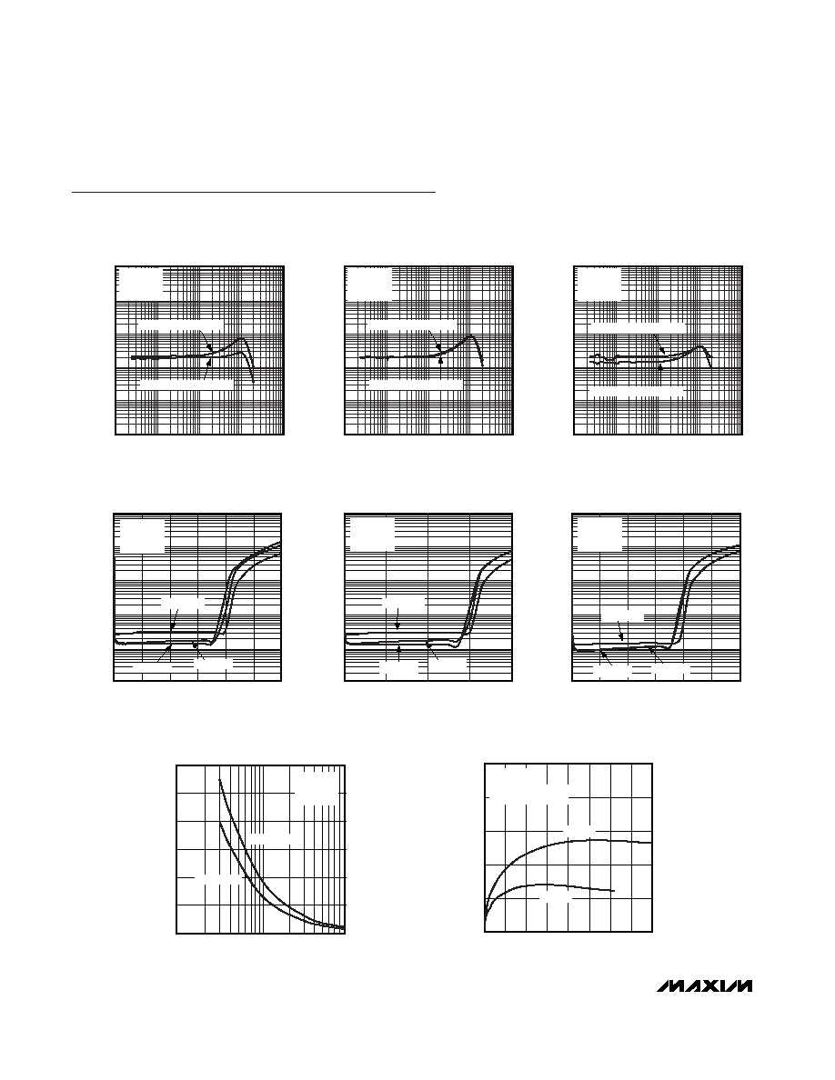
Typical Operating Characteristics
(Measurement BW = 22Hz to 22kHz, T
A
= +25∞C, unless otherwise noted.)
10
1
0.1
0.01
0.001
0.0001
10
1k
10k
100
100k
TOTAL HARMONIC DISTORTION PLUS NOISE
vs. FREQUENCY
MAX9787 toc01
FREQUENCY (Hz)
THD+N (%)
V
CC
= 5V
R
L
= 3
A
V
= 10.5dB
OUTPUT POWER = 1.5W
OUTPUT POWER = 500mW
10
1
0.1
0.01
0.001
0.0001
10
1k
10k
100
100k
TOTAL HARMONIC DISTORTION PLUS NOISE
vs. FREQUENCY
MAX9787 toc02
FREQUENCY (Hz)
THD+N (%)
V
CC
= 5V
R
L
= 4
A
V
= 10.5dB
OUTPUT POWER = 1.25W
OUTPUT POWER = 500mW
10
1
0.1
0.01
0.001
0.0001
10
1k
10k
100
100k
TOTAL HARMONIC DISTORTION PLUS NOISE
vs. FREQUENCY
MAX9787 toc03
FREQUENCY (Hz)
THD+N (%)
V
CC
= 5V
R
L
= 8
A
V
= 10.5dB
OUTPUT POWER = 100mW
OUTPUT POWER = 600mW
100
0
0.5
1.0
1.5
2.0
2.5
3.0
10
1
0.1
0.01
0.001
TOTAL HARMONIC DISTORTION PLUS NOISE
vs. OUTPUT POWER
MAX9787 toc04
OUTPUT POWER (W)
THD+N (%)
V
CC
= 5V
R
L
= 3
A
V
= 10.5dB
f
IN
= 10kHz
f
IN
= 1kHz
f
IN
= 20Hz
100
0
0.5
1.0
1.5
2.0
10
1
0.1
0.01
0.001
TOTAL HARMONIC DISTORTION PLUS NOISE
vs. OUTPUT POWER
MAX9787 toc05
OUTPUT POWER (W)
THD+N (%)
f
IN
= 1kHz
f
IN
= 20Hz
V
CC
= 5V
R
L
= 4
A
V
= 10.5dB
f
IN
= 10kHz
100
0
0.2
0.4
0.6
0.8
1.0
1.2
10
1
0.1
0.01
0.001
TOTAL HARMONIC DISTORTION PLUS NOISE
vs. OUTPUT POWER
MAX9787 toc06
OUTPUT POWER (W)
THD+N (%)
f
IN
= 20Hz
f
IN
= 1kHz
f
IN
= 10kHz
V
CC
= 5V
R
L
= 8
A
V
= 10.5dB
OUTPUT POWER
vs. LOAD RESISTANCE
MAX9787 toc07
LOAD RESISTANCE (
)
OUTPUT POWER (W)
3.0
0
0.5
1.0
1.5
2.0
2.5
1
10
100
THD+N = 10%
THD+N = 1%
V
CC
= 5V
f = 1kHz
A
V
= 10.5dB
POWER DISSIPATION vs. OUTPUT POWER
MAX9787 toc08
OUTPUT POWER (W)
POWER DISSIPATION (W)
3.5
3.0
2.5
2.0
1.5
1.0
0.5
1
2
3
4
5
0
0
4.0
R
L
= 4
R
L
= 8
V
DD
= 5V
f = 1kHz
P
OUT
= P
OUTL
+ P
OUTR
MAX9787
2.2W Stereo Audio Power Amplifier
with Analog Volume Control
_______________________________________________________________________________________
5
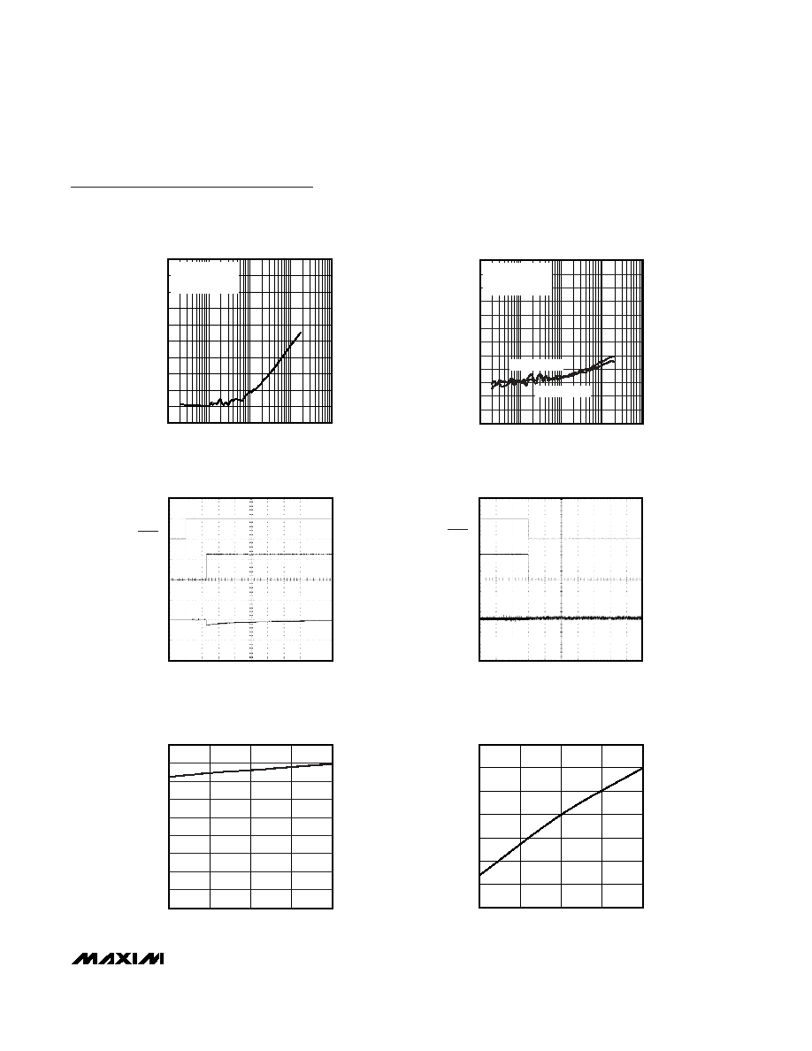
POWER-SUPPLY REJECTION RATIO
vs. FREQUENCY
MAX9787 toc09
FREQUENCY (Hz)
PSRR (dB)
10k
1k
100
-90
-80
-70
-60
-50
-40
-30
-20
-10
0
-100
10
100k
V
RIPPLE
= 200mV
P-P
A
V
= 10.5dB
OUTPUT REFERRED
TURN-ON RESPONSE
MAX9787 toc11
20ms/div
SHDN
5V/div
2V/div
100mV/div
OUT_+
AND
OUT_-
OUT_+
- OUT_-
R
L
= 8
TURN-OFF RESPONSE
MAX9787 toc12
20ms/div
SHDN
5V/div
2V/div
20mV/div
OUT_+
AND
OUT_-
OUT_+
- OUT_-
R
L
= 8
SUPPLY CURRENT
vs. SUPPLY VOLTAGE
MAX9787 toc13
SUPPLY VOLTAGE (V)
SUPPLY CURRENT (mA)
5.25
5.00
4.75
4
2
6
8
12
10
14
16
18
0
4.50
5.50
SHUTDOWN SUPPLY CURRENT
vs. SUPPLY VOLTAGE
MAX9787 toc14
SUPPLY VOLTAGE (V)
SUPPLY CURRENT (
µ
A)
5.25
5.00
4.75
4.50
5.50
0.05
0.10
0.15
0.20
0.25
0.30
0.35
0
0
-120
10
1k
10k
100
100k
CROSSTALK vs. FREQUENCY
MAX9787 toc10
FREQUENCY (Hz)
CROSSTALK (dB)
-100
-110
-80
-90
-60
-70
-40
-50
-20
-10
-30
V
CC
= 5V
V
RIPPLE
= 200mV
P-P
R
L
= 4
LEFT TO RIGHT
RIGHT TO LEFT
Typical Operating Characteristics (continued)
(Measurement BW = 22Hz to 22kHz, T
A
= +25∞C, unless otherwise noted.)