 | –≠–ª–µ–∫—Ç—Ä–æ–Ω–Ω—ã–π –∫–æ–º–ø–æ–Ω–µ–Ω—Ç: MAX9890 | –°–∫–∞—á–∞—Ç—å:  PDF PDF  ZIP ZIP |

General Description
The MAX9890 provides click-and-pop suppression for
devices such as CODECs with integrated headphone
amplifiers that lack a clickless/popless startup/power-
up or shutdown/power-down. The device controls the
ramping of the DC bias voltage on the output-coupling
capacitors and the application of the audio signal to
ensure that no audible transients are present at the
headphones. The MAX9890A features a 200ms startup
time for use with up to 100µF coupling capacitors. The
MAX9890B features a 330ms startup time for use with
greater than 100µF coupling capacitors.
The MAX9890 consumes 14µA of supply current and
0.001µA in shutdown, while contributing less than
0.003% THD+N into a 32
load. ESD (Human Body
Model) protection circuitry on the outputs protect the
MAX9890 and devices further up the signal chain from
ESD strikes up to ±8kV.
The MAX9890 is available in a miniature (1.5mm
1.5mm
0.6mm) 9-bump chip-scale package (UCSPTM),
as well as an 8-pin TDFN package (3mm
3mm
0.8mm), and is specified for operation over the
-40∞C to +85∞C extended temperature range.
Applications
High-End Notebook Audio
PDAs
Portable DVD Players
Cell Phones
Portable MP3 Players
Features
o 36dB Click-Pop Suppression
o 2.7V to 5.5V Single-Supply Operation
o Clickless/Popless Startup/Power-Up and
Shutdown/Power-Down
o 0.001µA Low-Power Shutdown Mode
o THD+N < 0.003% Into 32
o ±8kV ESD Protection (Human Body Model)
o Requires Only One 0.1µF Capacitor to Complete
the Circuit
o Low 14µA Supply Current
o Tiny Packaging
9-Bump UCSP (1.5mm x 1.5mm x 0.6mm)
8-Pin TDFN (3mm x 3mm x 0.8mm)
MAX9890
Audio Click-Pop Suppressor
________________________________________________________________ Maxim Integrated Products
1
Ordering Information
19-2932; Rev 0; 8/03
For pricing, delivery, and ordering information, please contact Maxim/Dallas Direct! at
1-888-629-4642, or visit Maxim's website at www.maxim-ic.com.
PART
TEMP RANGE
PIN-
PACKAGE
TOP
MARK
M AX 9890AE BL- T*
-40
∞C to +85∞C 9 UCSP-9
ADV
MAX9890AETA
-40
∞C to +85∞C 8 TDFN-EP**
AHA
M AX 9890BE BL- T*
-40
∞C to +85∞C 9 UCSP-9
ADW
MAX9890BETA
-40
∞C to +85∞C 8 TDFN-EP**
AHB
Selector Guide
PART
PIN-PACKAGE
SWITCH TURN-ON
TIME (ms)
MAX9890AEBL-T
9 UCSP-9
200
MAX9890AETA
8 TDFN-EP
200
MAX9890BEBL-T
9 UCSP-9
330
MAX9890BETA
8 TDFN-EP
330
UCSP is a trademark of Maxim Integrated Products, Inc.
*Future product--contact factory for availability.
**EP = Exposed pad.
Simplified Block Diagram
RAMP
UP
SINGLE SUPPLY
2.7V TO 5.5V
MAX9890
INL
INR
OUTL
OUTR
RAMP
DOWN
Typical Application Circuit and Pin Configurations appear
at end of data sheet.

MAX9890
Audio Click-Pop Suppressor
2
_______________________________________________________________________________________
ABSOLUTE MAXIMUM RATINGS
Stresses beyond those listed under "Absolute Maximum Ratings" may cause permanent damage to the device. These are stress ratings only, and functional
operation of the device at these or any other conditions beyond those indicated in the operational sections of the specifications is not implied. Exposure to
absolute maximum rating conditions for extended periods may affect device reliability.
(All Voltages are Referenced to GND)
V
CC
........................................................................................+6V
CEXT, SHDN, OUT_ .................................................-0.3V to +6V
IN_ ..............................................................-0.3V to (V
CC
+ 0.3V)
Continuous Current (IN_, OUT_).....................................±150mA
Continuous Current (All Other Pins) .................................±20mA
Continuous Power Dissipation (T
A
= +70∞C)
8-Pin TDFN (derate 24.4mW/∞C above +70∞C) ..........1951mW
9-Bump UCSP (derate 4.7mW/∞C above +70∞C)..........379mW
Operating Temperature Range ...........................-40∞C to +85∞C
Storage Temperature Range .............................-65∞C to +150∞C
Junction Temperature ......................................................+150∞C
Lead Temperature (soldering, 10s) .................................+300∞C
Bump Temperature (soldering)
Reflow ...........................................................................+235∞C
ELECTRICAL CHARACTERISTICS
(V
CC
= 3V, SHDN = V
CC
, GND = 0, C
CEXT
= 0.1µF, T
A
= T
MIN
to T
MAX
, unless otherwise noted. Typical values are at T
A
= +25∞C.)
(Note 1)
PARAMETER
SYMBOL
CONDITIONS
MIN
TYP
MAX
UNITS
Supply Voltage Range
V
CC
Inferred from R
ON
test
2.7
5.5
V
Supply Current
I
CC
(Note 2)
14
22
µA
Shutdown Supply Current
I
SHDN
SHDN = GND
0.001
1
µA
Input Voltage Range
Inferred from R
ON
test
0
V
CC
V
V
CC
= 5.5V
0.4
1
On-Resistance
R
ON
Over input voltage
range
V
CC
= 2.7V
0.7
1.5
On-Resistance Flatness
R
FLAT(ON)
Over input voltage range
2
m
Output Discharge Resistance
R
OUT(DIS)
220
k
Input Off-Leakage Current
SHDN = GND
0.001
1
µA
V
CC
Power-Down Threshold
(Note 3)
V
UVLO
V
CC
falling
2.5
V
Click-Pop Reduction
36
dB
ESD Protection
OUT_, Human Body Model
±8
kV
DYNAMIC
MAX9890A
200
Turn-On Time (Note 4)
t
ON
MAX9890B
330
ms
Turn-Off Time
t
OFF
(Note 5)
120
ns
Bandwidth
>100
kHz
Total Harmonic Distortion Plus
Noise
THD+N
R
L
= 32
, 30mW, f = 1kHz
0.003
%
Off-Isolation, IN_ to OUT_
f = 20kHz,
SHDN = GND, R
L
= 32
-108
dB
Crosstalk (Switches ON)
f = 20kHz
-100
dB
V
RIPPLE
= 0.5V
P-P
at 20Hz, f
IN
= 3kHz at
1V
P-P
, R
L
= 32
-100
V
RIPPLE
= 0.5V
P-P
at 1kHz, f
IN
= 3kHz at
1V
P-P
, R
L
= 32
-100
Power-Supply Rejection Ratio
(Note 6)
PSRR
V
RIPPLE
= 0.5V
P-P
at 20kHz, f
IN
= 3kHz
at 1V
P-P
, R
L
= 32
-84
dB
MAX9890
Audio Click-Pop Suppressor
_______________________________________________________________________________________
3
ELECTRICAL CHARACTERISTICS (continued)
(V
CC
= 3V, SHDN = V
CC
, GND = 0, C
CEXT
= 0.1µF, T
A
= T
MIN
to T
MAX
, unless otherwise noted. Typical values are at T
A
= +25∞C.)
(Note 1)
PARAMETER
SYMBOL
CONDITIONS
MIN
TYP
MAX
UNITS
LOGIC INPUT (
SHDN)
Logic-Input High Voltage
V
IH
V
CC
= 2.7V to 5.5V
2.0
V
Logic-Input Low Voltage
V
IL
V
CC
= 2.7V to 5.5V
0.8
V
Logic-Input Current
I
IN
±1
µA
Note 1: All devices are 100% tested at T
A
= +25∞C. All temperature limits are guaranteed by design.
Note 2: Supply current is measured when switch is on (i.e., SHDN = V
CC
, t > t
ON
).
Note 3: Supply voltage level where the device enters its power-down cycle.
Note 4: Turn-on time is measured from the time V
CC
= 3V and SHDN > V
IH
until the R
ON
specification is met.
Note 5: Switch turn-off time is measured from the time SHDN < V
IL
or V
CC
< V
UVLO
until the off-isolation specification is met.
Note 6: See the Power-Supply Rejection Ratio section for test method.
Typical Operating Characteristics
(V
CC
= 3V, C
CEXT
= 0.1µF, typical values are at T
A
= +25∞C, unless otherwise noted.)
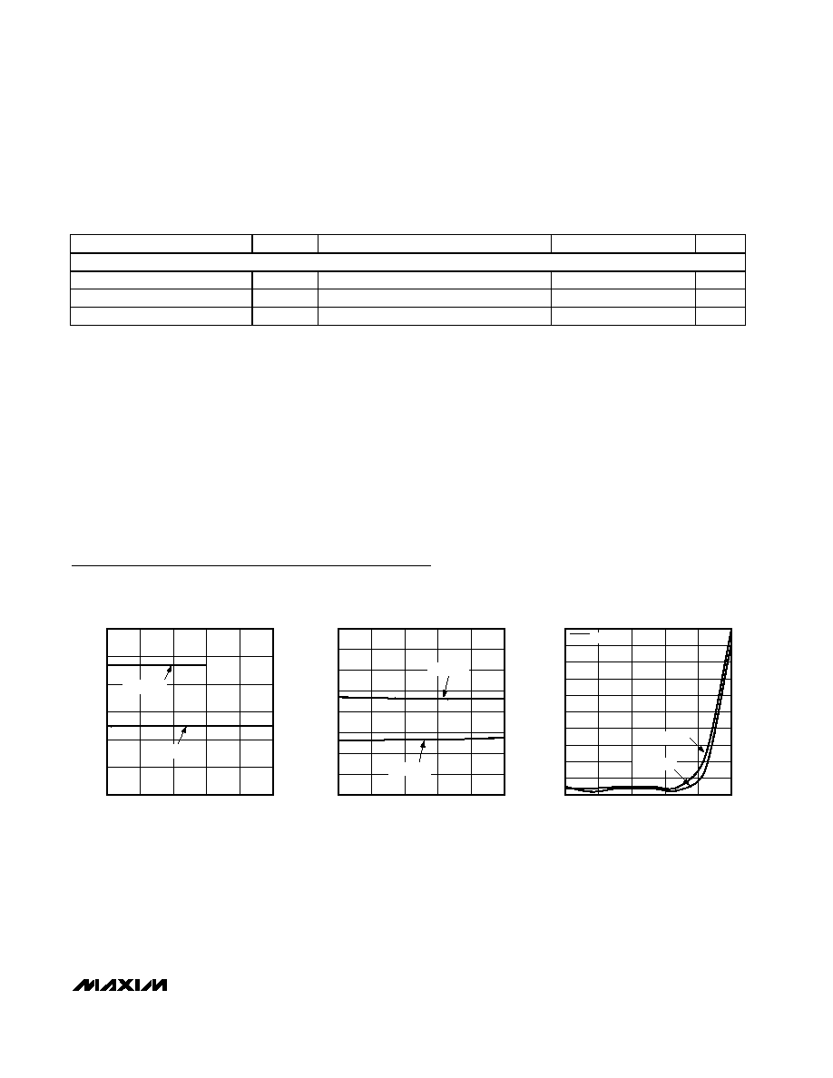
ON-RESISTANCE vs. IN_ VOLTAGE
MAX9890 toc01
IN_ VOLTAGE (V)
ON-RESISTANCE (
)
4
3
2
1
0.3
0.4
0.5
0.6
0.7
0.8
0.2
0
5
V
CC
= 3V
V
CC
= 5V
SUPPLY CURRENT vs. TEMPERATURE
MAX9890 toc02
TEMPERATURE (
∞C)
SUPPLY CURRENT (
µ
A)
60
35
-15
10
5
10
15
20
25
30
35
40
0
-40
85
V
CC
= 5.5V
V
CC
= 2.7V
SHUTDOWN CURRENT vs. TEMPERATURE
MAX9890 toc03
TEMPERATURE (
∞C)
SHUTDOWN CURRENT (pA)
60
35
10
-15
100
200
300
400
500
600
700
800
900
1000
0
-40
85
V
CC
= 2.7V
V
CC
= 5.5V
SHDN = 0V

MAX9890
Audio Click-Pop Suppressor
4
_______________________________________________________________________________________
FREQUENCY (Hz)
ON-LOSS (dB)
10k
1k
100
10
100k
ON-LOSS vs. FREQUENCY
MAX9890 toc04
-0.6
-0.2
0.2
0.6
1.0
-1.0
-0.8
-0.4
0
0.4
0.8
R
L
= 32
R
L
= 16
PHASE SHIFT (DEGREES)
-4
-3
-2
-1
0
1
2
-5
FREQUENCY (Hz)
100
10
PHASE SHIFT vs. FREQUENCY
MAX9890 toc05
R
L
= 32
R
L
= 16
10k
1k
100k
OFF-ISOLATION (dB)
-130
-110
-90
-70
-50
-30
-10
10
-150
FREQUENCY (Hz)
10k
1k
100
10
100k
OFF-ISOLATION vs. FREQUENCY
MAX9890 toc06
R
L
= 32
R
L
= 16
CROSSTALK (dB)
-140
-130
-120
-110
-100
-90
-80
-70
-60
-50
-150
FREQUENCY (Hz)
10k
1k
100
10
100k
CROSSTALK vs. FREQUENCY
MAX9890 toc07
TOTAL HARMONIC DISTORTION
PLUS NOISE vs. OUTPUT POWER
MAX9890 toc08
OUTPUT POWER (mW)
THD+N (%)
225
200
175
150
125
100
75
50
25
0.01
0.1
1
10
100
0.001
0
250
V
CC
= 5V
R
L
= 16
f = 1kHz
100
80
60
40
20
0
120
TOTAL HARMONIC DISTORTION
PLUS NOISE vs. OUTPUT POWER
MAX9890 toc09
OUTPUT POWER (mW)
THD+N (%)
0.01
0.1
1
10
100
0.001
V
CC
= 5V
R
L
= 32
f = 1kHz
TOTAL HARMONIC DISTORTION
PLUS NOISE vs. OUTPUT POWER
MAX9890 toc10
OUTPUT POWER (mW)
THD+N (%)
225
200
175
150
125
100
75
50
25
0.01
0.1
1
10
100
0.001
0
V
CC
= 3V
R
L
= 16
f = 1kHz
100
80
60
40
20
0
120
TOTAL HARMONIC DISTORTION
PLUS NOISE vs. OUTPUT POWER
MAX9890 toc11
OUTPUT POWER (mW)
THD+N (%)
0.01
0.1
1
10
100
0.001
V
CC
= 3V
R
L
= 32
f = 1kHz
FREQUENCY (Hz)
THD+N (%)
10k
1k
100
0.001
0.01
0.1
1
0.0001
10
100k
TOTAL HARMONIC DISTORTION
PLUS NOISE vs. FREQUENCY
MAX9890 toc12
V
CC
= 5V
R
L
= 16
OUTPUT POWER = 25mW
OUTPUT POWER = 150mW
Typical Operating Characteristics (continued)
(V
CC
= 3V, C
CEXT
= 0.1µF, typical values are at T
A
= +25∞C, unless otherwise noted.)

MAX9890
Audio Click-Pop Suppressor
_______________________________________________________________________________________
5
FREQUENCY (Hz)
THD+N (%)
10k
1k
100
0.001
0.01
0.1
1
0.0001
10
100k
TOTAL HARMONIC DISTORTION
PLUS NOISE vs. FREQUENCY
MAX9890 toc13
V
CC
= 5V
R
L
= 32
OUTPUT POWER = 20mW
OUTPUT POWER = 80mW
FREQUENCY (Hz)
THD+N (%)
10k
1k
100
0.001
0.01
0.1
1
0.0001
10
100k
TOTAL HARMONIC DISTORTION
PLUS NOISE vs. FREQUENCY
MAX9890 toc14
V
CC
= 3V
R
L
= 16
OUTPUT POWER = 100mW
OUTPUT POWER = 25mW
FREQUENCY (Hz)
THD+N (%)
10k
1k
100
0.001
0.01
0.1
1
0.0001
10
100k
TOTAL HARMONIC DISTORTION
PLUS NOISE vs. FREQUENCY
MAX9890 toc15
V
CC
= 3V
R
L
= 32
OUTPUT POWER = 60mW
OUTPUT POWER = 20mW
SHDN
2V/div
V
OUT
1V/div
V
HEADPHONE
10mV/div
40ms/div
STARTUP WAVEFORM (DC)
MAX9890 toc16
SHDN
2V/div
V
OUT
1V/div
V
HEADPHONE
10mV/div
10s/div
SHUTDOWN WAVEFORM (DC)
MAX9890 toc17
SHDN
2V/div
V
OUT
1V/div
V
HEADPHONE
1V/div
40ms/div
STARTUP WAVEFORM (AC)
MAX9890 toc18
SHDN
2V/div
V
OUT
1V/div
V
HEADPHONE
1V/div
1s/div
SHUTDOWN WAVEFORM (AC)
MAX9890 toc19
Typical Operating Characteristics (continued)
(V
CC
= 3V, C
CEXT
= 0.1µF, typical values are at T
A
= +25∞C, unless otherwise noted.)