 | ÐлекÑÑоннÑй компоненÑ: MAX9987 | СкаÑаÑÑ:  PDF PDF  ZIP ZIP |
Äîêóìåíòàöèÿ è îïèñàíèÿ www.docs.chipfind.ru
General Description
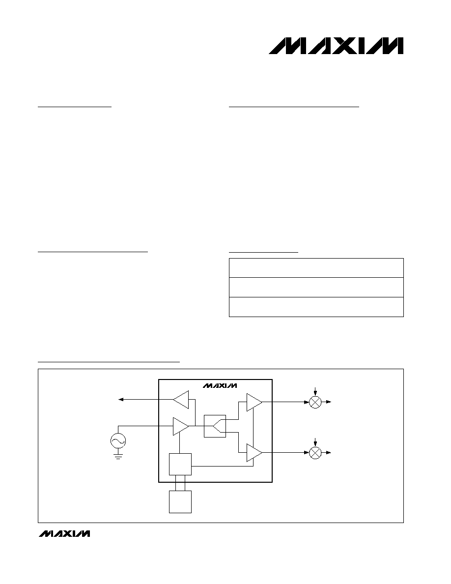
The MAX9987 and MAX9988 LO buffers/splitters each
integrate a passive two-way power splitter with high-
isolation input and output buffer amplifiers. These
buffers are designed to provide the high output
(+14dBm to +20dBm) necessary to drive the LO inputs
of high-linearity passive mixers, while offering 40dB
reverse isolation to prevent LO pulling. The MAX9987 is
internally matched for the cellular/GSM bands, and the
MAX9988 is matched for the DCS/PCS/UMTS bands.
The typical application circuit provides a nominal
+17dBm output power with ±1dB variation over supply,
temperature, and input power. With two optional resis-
tors, the output power can be precision set from
+14dBm to +20dBm. The devices offer more than 30dB
output-to-output port isolation, and are offered in 5mm
5mm 20-pin QFN packages with exposed paddle.
Applications
Cellular/GSM/DCS/PCS/UMTS Base Station
Tx/Rx LO Drive
Base Station Main and Diversity Channels
Coherent Receivers
ISM Wireless LAN
Wireless Local Loop
Local Multipoint Distribution Service
Point-to-Point Systems
Features
o ±1dB Output Power Variation
o +14dBm to +20dBm Adjustable Output Power
o Two-Way Power Splitting
o 40dB Reverse Isolation
o More than 30dB Output-to-Output Isolation
o Low Output Noise: -170dBc/Hz at +17dBm
o 160mA Supply Current at +17dBm
o ESD Protection
o Isolated PLL Output (+3dBm)
MAX9987/MAX9988
+14dBm to +20dBm LO Buffers/Splitters
with ±1dB Variation
________________________________________________________________ Maxim Integrated Products
1
MAX9987
MAX9988
BIAS
BIASIN
RF LO
TO PLL
PRESCALER
PLL BUFFER
INPUT AMP
OUTPUT AMP
(2)
OUTPUT AMP
(1)
RF INPUT
(1)
IF OUTPUT
(1)
PASSIVE TWO-WAY
POWER SPLITTER
IN
(+7dBm)
OUTPLL
(+3dBm)
OUT1
(+17dBm)
OUT2
(+17dBm)
BIASOUT
BIAS
CONTROL
NETWORK
RF INPUT
(2)
IF OUTPUT
(2)
Typical Operating Circuit and Block Diagram
Ordering Information
19-2416; Rev 0; 4/02
For pricing, delivery, and ordering information, please contact Maxim/Dallas Direct! at
1-888-629-4642, or visit Maxim's website at www.maxim-ic.com.
PART
TEMP
RANGE
PIN-
PACKAGE
FREQUENCY
RANGE
MAX9987EGP
-40
°C to 85°C 20 QFN-EP*
700MHz to
1100MHz
MAX9988EGP
-40
°C to 85°C 20 QFN-EP*
1500MHz to
2200MHz
*EP = Exposed paddle
MAX9987/MAX9988
+14dBm to +20dBm LO Buffers/Splitters
with ±1dB Variation
2
_______________________________________________________________________________________
ABSOLUTE MAXIMUM RATINGS
Stresses beyond those listed under "Absolute Maximum Ratings" may cause permanent damage to the device. These are stress ratings only, and functional
operation of the device at these or any other conditions beyond those indicated in the operational sections of the specifications is not implied. Exposure to
absolute maximum rating conditions for extended periods may affect device reliability.
VCC1, VCC2, VCC3,
VCCREF to GND.................................................-0.3V to +6.0V
IN to GND ...................................................-0.3V to (V
CC
+ 0.3V)
OUT1, OUT2,
OUTPLL to GND ......................................-0.3V to (V
CC
+ 0.3V)
REF to GND ......................................................Source/Sink 5mA
INBIAS, OUTBIAS, to GND..................................-0.3V to +0.75V
PLLBIAS ......................................................................Sink 25mA
RF Input Power ...............................................................+20dBm
Continuous Power Dissipation (T
A
= +70°C)
5mm
5mm 20-Pin QFN (derate 20mW/°C
above +70°C).............................................................1600mW
JA
....................................................................................50°C/W
Junction Temperature ......................................................+150°C
Operating Temperature Range ...........................-40°C to +85°C
Storage Temperature Range .............................-65°C to +150°C
Lead Temperature (soldering, 10s) .................................+300°C
DC ELECTRICAL CHARACTERISTICS--MAX9987
(Typical Application Circuit, V
CC
= 4.75V to 5.25V, input and outputs terminated in 50
, T
A
= -40°C to +85°C. Typical specifications
are for V
CC
= 5.0V and T
A
= +25°C.) (Note 1)
PARAMETER
SYMBOL
CONDITIONS
MIN
TYP
MAX
UNITS
Supply Voltage
V
CC
4.75
5.00
5.25
V
Low power setting
(see Table 1 for resistor values)
110
Nominal power setting
(R
1
, R
2
, R
4
, and R
5
not installed)
139
155
171
Supply Current
I
CC
High power setting
(see Table 1 for resistor values)
221
mA
DC ELECTRICAL CHARACTERISTICS--MAX9988
(Typical Application Circuit, V
CC
= 4.75V to 5.25V, input and outputs terminated in 50
, T
A
= -40°C to +85°C. Typical specifications
are for V
CC
= 5.0V and T
A
= +25°C.) (Note 1)
PARAMETER
SYMBOL
CONDITIONS
MIN
TYP
MAX
UNITS
Supply Voltage
V
CC
4.75
5.00
5.25
V
Low power setting
(see Table 1 for resistor values)
120
Nominal power setting
(R
1
, R
2
, R
4
, and R
5
not installed)
150
162
175
Supply Current
I
CC
High power setting
(see Table 1 for resistor values)
229
mA
MAX9987/MAX9988
+14dBm to +20dBm LO Buffers/Splitters
with ±1dB Variation
_______________________________________________________________________________________
3
AC ELECTRICAL CHARACTERISTICS--MAX9987
(Typical Application Circuit, V
CC
= 4.75V to 5.25V, 50
environment, +4dBm < P
IN
< +10dBm, 700MHz < f
IN
< 1100MHz,
T
A
= -40°C to +85°C, unless otherwise noted. Typical specifications are for V
CC
= 5.0V, P
IN
= +7dBm, f
IN
= 900MHz, and
T
A
= +25°C, unless otherwise noted.) (Note 1)
PARAMETER
SYMBOL
CONDITIONS
MIN
TYP
MAX
UNITS
Operating Frequency
f
700
1100
MHz
Low power setting, P
IN
= +4dBm
(see Table 1 for resistor values)
14.3
Nominal power setting,
+4dBm < P
IN
< +10dBm, 4.75V < V
CC
<
5.25V, -40°C < T
A
< +85°C
(R
1
, R
2
,
R
4
, and R
5
not installed)
17.3
±0.8
Output Power (Main Drivers)
P
OUTLO
High power setting, P
IN
= +10dBm
(see Table 1 for resistor values)
19.7
dBm
Output Power (PLL Driver)
P
OUTPLL
3.7
dBm
Input VSWR
VSWR
IN
1.2:1
Output VSWR
VSWR
OUT
1.7:1
Output-Noise Power Density
P
NOISE
V
CC
= 5.0V, ±100MHz offset
(R
1
, R
2
,
R
4
, and R
5
not installed)
-152
dBm/Hz
OUT1 to OUT2 Isolation
S23
V
CC
= 5.0V, nominal power setting
(R
1
, R
2
,
R
4
, and R
5
not installed)
45
dB
OUT2 to OUT1 Isolation
S32
V
CC
= 5.0V, nominal power setting
(R
1
, R
2
,
R
4
, and R
5
not installed)
39
dB
OUT1 to RFIN Isolation
S12
V
CC
= 5.0V, nominal power setting
(R
1
, R
2
,
R
4
, and R
5
not installed)
48
dB
OUT2 to RFIN Isolation
S13
V
CC
= 5.0V, nominal power setting
(R
1
, R
2
,
R
4
, and R
5
not installed)
50
dB
MAX9987/MAX9988
+14dBm to +20dBm LO Buffers/Splitters
with ±1dB Variation
4
_______________________________________________________________________________________
PARAMETER
SYMBOL
CONDITIONS
MIN
TYP
MAX
UNITS
Operating Frequency
f
1500
2200
MHz
Low power setting, P
IN
= +6dBm
(see Table 1 for resistor values)
14.2
Nominal power setting,
+6dBm < P
IN
< +12dBm, 4.75V < V
CC
<
5.25V, -40°C < T
A
< +85°C
(R
1
, R
2
,
R
4
, and R
5
not installed)
17.3
±0.8
Output Power
(Main Drivers)
P
OUTLO
High power setting, P
IN
= +12dBm
(see Table 1 for resistor values)
19.5
dBm
Output Power
(PLL Driver)
P
OUTPLL
3.6
dBm
Input VSWR
VSWR
IN
1.5:1
Output VSWR
VSWR
OUT
1.4:1
Output-Noise Power Density
P
NOISE
V
CC
= 5.0V, ±100MHz offset
-152
dBm/Hz
OUT1 to OUT2 Isolation
S23
V
CC
= 5.0V, nominal power setting
(R
1
, R
2
,
R
4
, and R
5
not installed)
33
dB
OUT2 to OUT1 Isolation
S32
V
CC
= 5.0V, nominal power setting
(R
1
, R
2
,
R
4
, and R
5
not installed)
44
dB
OUT1 to RFIN Isolation
S12
V
CC
= 5.0V, nominal power setting
(R
1
, R
2
,
R
4
, and R
5
not installed)
49
dB
OUT2 to RFIN Isolation
S13
V
CC
= 5.0V, nominal power setting
(R
1
, R
2
,
R
4
, and R
5
not installed)
47
dB
AC ELECTRICAL CHARACTERISTICS--MAX9988
(Typical Application Circuit, V
CC
= 4.75V to 5.25V, 50
environment, +6dBm < P
IN
< +12dBm, 1500MHz < f
IN
< 2200MHz, and
T
A
= -40°C to +85°C, unless otherwise noted. Typical specifications are for V
CC
= 5.0V, P
IN
= +9dBm, f
IN
= 1800MHz, and
T
A
= +25°C unless otherwise noted.) (Note 1)
Note 1: Devices are 100% DC screened and AC production tested for functionality. Data sheet typical specifications are derived
from the average of 30 units from a typical lot, and are tested under the conditions specified for the typical specifications.
MAX9987/MAX9988
+14dBm to +20dBm LO Buffers/Splitters
with ±1dB Variation
_______________________________________________________________________________________
5
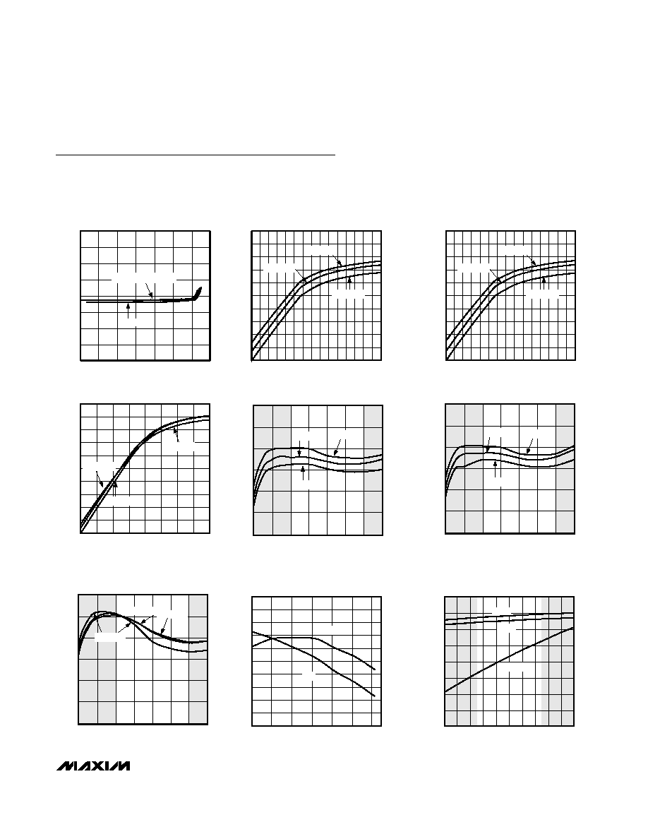
SUPPLY CURRENT vs. OUTPUT POWER
OUTMAIN
MAX9987 toc01
OUTPUT POWER (dBm)
SUPPLY CURRENT (mA)
20
15
10
5
0
-5
-10
145
150
155
160
165
170
180
140
-15
175
T
A
= -40
°C
T
A
= +25
°C AND +85°C
OUTPUT POWER vs. INPUT POWER
OUT1
MAX9987 toc02
INPUT POWER (dBm)
OUTPUT POWER (dBm)
9
2 3
-3
-4
11
12
13
14
15
16
17
18
19
20
10
-5
10
8
7
-2 -1 0 1
4 5 6
T
A
= +85
°C
T
A
= +25
°C
T
A
= -40
°C
OUTPUT POWER vs. INPUT POWER
OUT2
MAX9987 toc03
INPUT POWER (dBm)
OUTPUT POWER (dBm)
9
2 3
-3
-4
11
12
13
14
15
16
17
18
19
20
10
-5
10
8
7
-2 -1 0 1
4 5 6
T
A
= +85
°C
T
A
= +25
°C
T
A
= -40
°C
OUTPUT POWER vs. INPUT POWER, OUTPLL
MAX9987 toc04
INPUT POWER (dBm)
OUTPUT POWER (dBm)
8
6
2
4
-2
0
-4
-4
-3
-2
-1
0
1
2
3
4
5
-5
-6
10
T
A
= +85
°C
T
A
= +25
°C
T
A
= -40
°C
OUTPUT POWER vs. FREQUENCY, OUT1
MAX9987 toc05
OPERATING FREQUENCY (MHz)
OUTPUT POWER (dBm)
1200
800
700
600
15
16
17
18
20
14
500
19
900 1000 1100
T
A
= +85
°C
T
A
= +25
°C
T
A
= -40
°C
OUTPUT POWER vs. FREQUENCY, OUT2
MAX9987 toc06
OPERATING FREQUENCY (MHz)
OUTPUT POWER (dBm)
1200
800
700
600
15
16
17
18
20
14
500
19
900
1000 1100
T
A
= +85
°C
T
A
= +25
°C
T
A
= -40
°C
OUTPUT POWER vs. FREQUENCY, PLL
MAX9987 toc07
OPERATING FREQUENCY (MHz)
OUTPUT POWER (dBm)
1200
800
700
600
1
2
3
4
6
0
500
5
900 1000 1100
T
A
= +85
°C
T
A
= +25
°C
T
A
= -40
°C
OUTPUT POWER AND SUPPLY CURRENT
vs. TEMPERATURE
MAX9987 toc08
AMBIENT TEMPERATURE (
°C)
OUTPUT POWER (dBm)
80
60
20
40
0
-20
16.2
16.4
16.6
16.8
17.0
17.2
17.4
17.6
17.8
18.0
16.0
-40
I
CC
160.2
160.4
160.6
160.8
161.0
161.2
161.4
161.6
161.8
162.0
160.0
SUPPLY CURRENT (mA)
P
OUT
OUTPUT POWER vs. SUPPLY VOLTAGE
MAX9987 toc09
SUPPLY VOLTAGE (V)
OUT1, OUT2 OUTPUT POWER (dBm)
5.5
4.9
4.8
4.7
4.6
14.5
15.0
15.5
16.0
16.5
17.0
18.0
14.0
4.5
17.5
OUT2
5.0 5.1 5.2 5.3 5.4
2.5
3.0
3.5
4.0
4.5
5.0
6.0
2.0
5.5
OUT1
OUTPLL
PLL OUTPUT POWER (dBm)
Typical Operating Characteristics
(V
CC
= 5.0V, nominal bias, f
IN
= 900MHz, P
IN
= +7dBm, T
A
= +25°C, unless otherwise noted.) (Shaded regions are outside the
guaranteed operating range, and are provided for reference only.)
MAX9987