 | –≠–ª–µ–∫—Ç—Ä–æ–Ω–Ω—ã–π –∫–æ–º–ø–æ–Ω–µ–Ω—Ç: MAX9989 | –°–∫–∞—á–∞—Ç—å:  PDF PDF  ZIP ZIP |
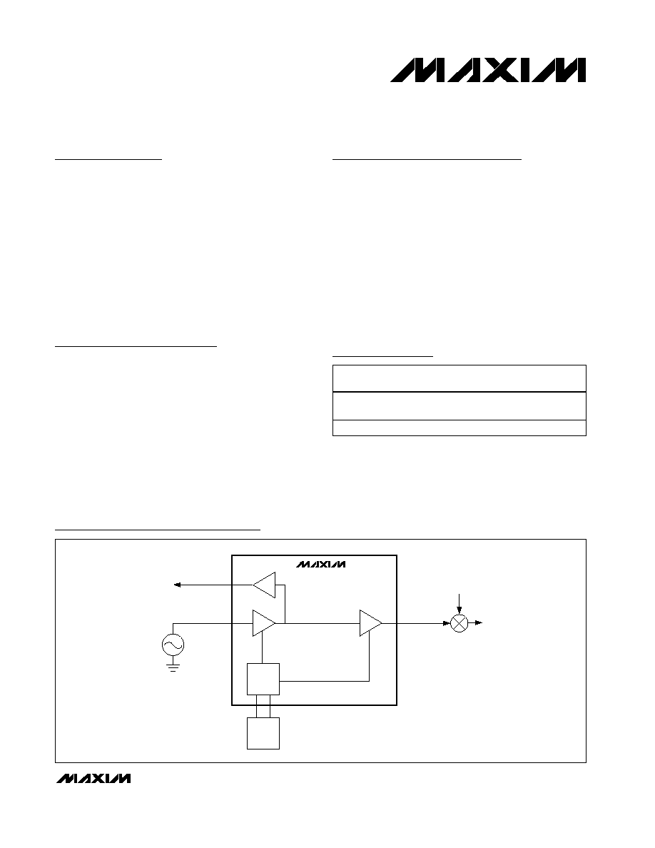
General Description
The MAX9989 and MAX9990 LO buffers provide the high
output (+14dBm to +20dBm) necessary to drive the LO
inputs of high-linearity passive mixers, while offering 40dB
reverse isolation to prevent LO pulling. The MAX9989 is
internally matched for the cellular/GSM bands, and the
MAX9990 is matched for the DCS/PCS/UMTS bands.
The Typical Application Circuit provides a nominal
+17dBm output power with ±1dB variation over supply,
temperature, and input power. With two optional resis-
tors, the output power can be precision set from
+14dBm to +20dBm. The devices offer more than 35dB
main driver output to PLL amp output isolation. Each
device is offered in a 5mm
5mm 20-pin thin QFN
package with exposed paddle.
Applications
Cellular/GSM/DCS/PCS/UMTS Base Station
Tx/Rx LO Drives
Coherent Receivers
ISM Wireless LAN
Wireless Local Loop
Local Multipoint Distribution Service
Point-to-Point Systems
Features
o ±1dB Output Power Variation
o +14dBm to +20dBm Adjustable Output Power
o 40dB Reverse Isolation
o Better Than 35dB Main Driver Output to PLL Amp
Output Isolation
o Low Output Noise: -170dBc/Hz at +17dBm
o 110mA Supply Current at +17dBm
o ESD Protection
o Isolated PLL Output (+3dBm)
MAX9989/MAX9990
+14dBm to +20dBm LO Buffers
with ±1dB Variation
________________________________________________________________ Maxim Integrated Products
1
MAX9989
MAX9990
BIAS
BIASIN
RF LO
TO PLL
PRESCALER
PLL BUFFER
INPUT AMP
OUTPUT AMP
RF INPUT
IF OUTPUT
IN
(+7dBm)
OUTPLL
(+3dBm)
OUTLO
(+17dBm)
BIASOUT
BIAS
CONTROL
NETWORK
Typical Operating Circuit and Block Diagram
Ordering Information
19-2486; Rev 0; 7/02
For pricing, delivery, and ordering information, please contact Maxim/Dallas Direct! at
1-888-629-4642, or visit Maxim's website at www.maxim-ic.com.
PART
TEMP
RANGE
PIN-
PACKAGE
FREQUENCY
RANGE (MHz)
MAX9989ETP -40
∞C to +85∞C
20 Thin
QFN-EP*
700 to 1100
MAX9990ETP -40
∞C to +85∞C 20 QFN-EP* 1500 to 2200
*EP = Exposed paddle.
Typical Application Circuit/Pin Configuration appears at end of data sheet.

MAX9989/MAX9990
+14dBm to +20dBm LO Buffers
with ±1dB Variation
2
_______________________________________________________________________________________
ABSOLUTE MAXIMUM RATINGS
Stresses beyond those listed under "Absolute Maximum Ratings" may cause permanent damage to the device. These are stress ratings only, and functional
operation of the device at these or any other conditions beyond those indicated in the operational sections of the specifications is not implied. Exposure to
absolute maximum rating conditions for extended periods may affect device reliability.
VCC1, VCC2, VCC3, VCCREF to GND .................-0.3V to +6.0V
IN to GND ...................................................-0.3V to (V
CC
+ 0.3V)
OUTLO, OUTPLL to GND...........................-0.3V to (V
CC
+ 0.3V)
REF to GND ......................................................Source/Sink 5mA
INBIAS, OUTBIAS to GND...................................-0.3V to +0.75V
PLLBIAS ......................................................................Sink 25mA
RF Input Power ...............................................................+20dBm
Continuous Power Dissipation (T
A
= +70∞C)
20-Pin Thin QFN (derate 21mW/∞C above +70∞C) ....1667mW
JA
.................................................................................+48∞C/W
Junction Temperature ......................................................+150∞C
Operating Temperature Range ...........................-40∞C to +85∞C
Storage Temperature Range .............................-65∞C to +150∞C
Lead Temperature (soldering, 10s) .................................+300∞C
DC ELECTRICAL CHARACTERISTICS--MAX9989
(Typical Application Circuit, V
CC
= 4.75V to 5.25V, input and outputs terminated in 50
, T
A
= -40∞C to +85∞C. Typical specifications
are for V
CC
= 5.0V and T
A
= +25∞C.) (Note 1)
PARAMETER
SYMBOL
CONDITIONS
MIN
TYP
MAX
UNITS
Supply Voltage
V
CC
4.75
5.00
5.25
V
Low power setting
(see Table 1 for resistor values)
77
Nominal power setting
(R2≠R5 not installed) (Note 2)
94
105
116
Supply Current
I
CC
High power setting
(see Table 1 for resistor values)
146
mA
DC ELECTRICAL CHARACTERISTICS--MAX9990
(Typical Application Circuit, V
CC
= 4.75V to 5.25V, input and outputs terminated in 50
, T
A
= -40∞C to +85∞C. Typical specifications
are for V
CC
= 5.0V and T
A
= +25∞C.) (Note 1)
PARAMETER
SYMBOL
CONDITIONS
MIN
TYP
MAX
UNITS
Supply Voltage
V
CC
4.75
5.00
5.25
V
Low power setting
(see Table 1 for resistor values)
87
Nominal power setting
(R2≠R5 not installed) (Note 2)
98
111
122
Supply Current
I
CC
High power setting
(see Table 1 for resistor values)
154
mA
MAX9989/MAX9990
+14dBm to +20dBm LO Buffers
with ±1dB Variation
_______________________________________________________________________________________
3
AC ELECTRICAL CHARACTERISTICS--MAX9989
(Typical Application Circuit, V
CC
= 4.75V to 5.25V, 50
environment, +4dBm < P
IN
< +10dBm, 700MHz < f
IN
< 1100MHz,
T
A
= -40∞C to +85∞C, unless otherwise noted. Typical specifications are for V
CC
= 5.0V, P
IN
= +7dBm, f
IN
= 900MHz, and
T
A
= +25∞C, unless otherwise noted.) (Note 1)
PARAMETER
SYMBOL
CONDITIONS
MIN
TYP
MAX
UNITS
Operating Frequency
f
700
1100
MHz
Low power setting, P
IN
= +4dBm
(see Table 1 for resistor values)
14.3
Nominal power setting,
+4dBm < P
IN
< +10dBm
4.75V < V
CC
< 5.25V
-40∞C < T
A
< +85∞C (R2≠R5 not installed)
17.3
±0.8
Output Power
P
OUTLO
High power setting, P
IN
= +10dBm
(see Table 1 for resistor values)
19.7
dBm
Output Power (PLL Driver)
P
OUTPLL
3.7
dBm
Input VSWR
VSWR
IN
1.2:1
Output VSWR
VSWR
OUT
1.7:1
Output-Noise Power Density
P
NOISE
V
CC
= 5.0V, ±100MHz offset
(R2≠R5 not installed)
-152
dBm/Hz
OUTLO to RFIN Isolation
S12
V
CC
= 5.0V, nominal power setting
(R2≠R5 not installed)
48
dB
PARAMETER
SYMBOL
CONDITIONS
MIN
TYP
MAX
UNITS
Operating Frequency
f
1500
2200
MHz
Low power setting, P
IN
= +6dBm
(see Table 1 for resistor values)
14.2
Nominal power setting,
+6dBm < P
IN
< +12dBm
4.75V < V
CC
< 5.25V
-40∞C < T
A
< +85∞C (R2≠R5 not installed)
17.3
±0.8
Output Power
P
OUTLO
High power setting, P
IN
= +12dBm
(see Table 1 for resistor values)
19.5
dBm
Output Power (PLL Driver)
P
OUTPLL
3.6
dBm
Input VSWR
VSWR
IN
1.5:1
Output VSWR
VSWR
OUT
1.4:1
Output-Noise Power Density
P
NOISE
V
CC
= 5.0V, ±100MHz offset
-152
dBm/Hz
OUTLO to RFIN Isolation
S12
V
CC
= 5.0V, nominal power setting
(R2≠R5 not installed)
49
dB
AC ELECTRICAL CHARACTERISTICS--MAX9990
(Typical Application Circuit, V
CC
= 4.75V to 5.25V, 50
environment, +6dBm < P
IN
< +12dBm, 1500MHz < f
IN
< 2200MHz, and
T
A
= -40∞C to +85∞C, unless otherwise noted. Typical specifications are for V
CC
= 5.0V, P
IN
= +9dBm, f
IN
= 1800MHz, and
T
A
= +25∞C, unless otherwise noted.) (Note 1)
Note 1: Devices are 100% DC screened and AC production tested for functionality. Data sheet typical specifications are derived
from the average of 30 units from a typical lot, and are tested under the conditions specified for the typical specifications.
Note 2: DC current limits at -40∞C are guaranteed by design and characterization.
MAX9989/MAX9990
+14dBm to +20dBm LO Buffers
with ±1dB Variation
4
_______________________________________________________________________________________
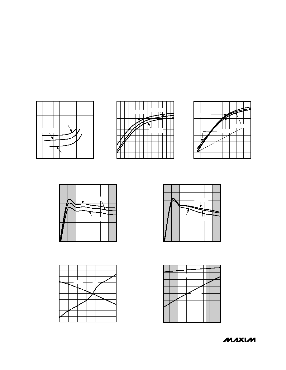
MAX9989 toc01
OUTPUT POWER (dBm)
SUPPLY CURRENT (mA)
19
18
17
16
15
14
13
12
11
105
110
115
120
100
10
20
T
A
= +85
∞C
T
A
= +25
∞C
T
A
= -40
∞C
SUPPLY CURRENT vs. OUTPUT POWER
OUTLO
20
19
18
17
16
15
14
13
12
11
10
-5
-3 -2
-4
0
-1
2
1
3 4 5 6 7 8 9 10
MAX9989 toc02
INPUT POWER (dBm)
OUTPUT POWER (dBm)
OUTPUT POWER vs. INPUT POWER
OUTLO
T
A
= +85
∞C
T
A
= +25
∞C
T
A
= -40
∞C
MAX9989 toc03
INPUT POWER (dBm)
OUTPUT POWER (dBm)
8
6
2
4
-2
0
-4
-3
-2
-1
0
1
2
3
4
5
6
-4
-6
10
OUTPUT POWER vs. INPUT POWER
OUTPLL
T
A
= +85
∞C
T
A
= +25
∞C
T
A
= -40
∞C
MAX9989 toc04
OPERATING FREQUENCY (MHz)
OUTPUT POWER (dBm)
1100
1000
900
800
700
600
15
16
17
18
19
20
14
500
1200
OUTPUT POWER vs. FREQUENCY
OUTLO
T
A
= +85
∞C
T
A
= +25
∞C
T
A
= -40
∞C
MAX9989 toc05
OPERATING FREQUENCY (MHz)
OUTPUT POWER (dBm)
1100
1000
900
800
700
600
1
2
3
4
5
6
7
0
500
1200
OUTPUT POWER vs. FREQUENCY
OUTPLL
T
A
= -40
∞C
T
A
= +25
∞C
T
A
= +85
∞C
AMBIENT TEMPERATURE (
∞C)
OUTPUT POWER (dBm)
80
60
20
40
0
-20
16.2
16.4
16.6
16.8
17.0
17.2
17.4
17.6
17.8
18.0
16.0
107.5
108.0
108.5
109.0
109.5
110.0
110.5
111.0
111.5
112.0
107.0
-40
OUTPUT POWER AND SUPPLY CURRENT
vs. TEMPERATURE
MAX9989 toc06
SUPPLY CURRENT (mA)
P
OUTLO
I
CC
OUTPUT POWER vs. SUPPLY VOLTAGE
SUPPLY VOLTAGE (V)
OUTLO OUTPUT POWER (dBm)
5.3
4.7
5.1
4.9
14.5
15.0
15.5
16.0
16.5
17.0
17.5
18.0
14.0
4.5
5.5
MAX9989 toc07
6.0
5.0
4.5
4.0
3.5
3.0
2.5
2.0
5.5
OUTPLL OUTPUT POWER (dBm)
OUTLO
OUTPLL
Typical Operating Characteristics
(V
CC
= 5.0V, nominal bias, f
IN
= 900MHz, P
IN
= +7dBm, T
A
= +25∞C, unless otherwise noted.) (Shaded regions are outside the
guaranteed operating range, and are provided for reference only.)
MAX9989
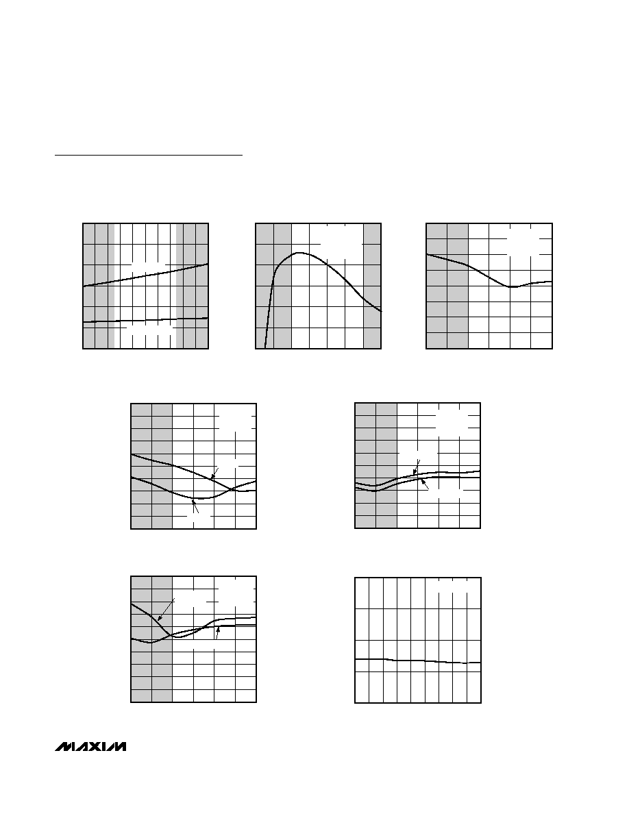
MAX9989/MAX9990
+14dBm to +20dBm LO Buffers
with ±1dB Variation
_______________________________________________________________________________________
5
MAX9989 toc08
SUPPLY VOLTAGE (V)
SUPPLY CURRENT (mA)
5.3
5.1
4.9
4.7
95
100
105
110
115
120
90
4.5
5.5
SUPPLY CURRENT vs. SUPPLY VOLTAGE
PLL BIASED
PLL NOT BIASED
SMALL-SIGNAL GAIN vs. FREQUENCY
MAX9989 toc09
FREQUENCY (MHz)
GAIN (dB)
1100
1000
900
800
700
600
14
15
16
17
18
19
13
500
1200
V
CC
= 5V
T
A
= +25
∞C
P
IN
= -15dBm
NOMINAL BIAS
INPUT RETURN LOSS vs. FREQUENCY
MAX9989 toc10
FREQUENCY (MHz)
RETURN LOSS (dB)
1000
900
600
700
800
-35
-30
-25
-20
-15
-10
-5
0
-40
500
1100
V
CC
= 5V
T
A
= +25
∞C
P
IN
= +7dBm
Typical Operating Characteristics (continued)
(V
CC
= 5.0V, nominal bias, f
IN
= 900MHz, P
IN
= +7dBm, T
A
= +25∞C, unless otherwise noted.) (Shaded regions are outside the
guaranteed operating range, and are provided for reference only.)
OUTPUT RETURN LOSS vs. FREQUENCY
MAX9989 toc11
FREQUENCY (MHz)
RETURN LOSS (dB)
1000
900
800
700
600
18
16
14
12
10
8
6
4
2
0
20
500
1100
V
CC
= 5V
T
A
= +25
∞C
P
IN
= +7dBm
OUTLO
OUTPLL
OUT-TO-IN ISOLATION vs. FREQUENCY
MAX9989 toc12
FREQUENCY (MHz)
ISOLATION (dB)
1000
900
800
700
600
-65
-60
-55
-50
-45
-40
-35
-30
-25
-20
-70
500
1100
V
CC
= 5V
T
A
= +25
∞C
P
IN
= +7dBm
OUTPLL TO IN
OUTLO TO IN
PLL ISOLATION vs. FREQUENCY
MAX9989 toc13
FREQUENCY (MHz)
ISOLATION (dB)
1000
900
800
700
600
-65
-60
-55
-50
-45
-40
-35
-30
-25
-20
-70
500
1100
V
CC
= 5V
T
A
= +25
∞C
P
IN
= +7dBm
OUTPLL TO
OUTLO
OUTLO TO OUTPLL
OUTPUT NOISE POWER vs. INPUT POWER
MAX9989 toc14
INPUT POWER (dBm)
NOISE POWER (dBm/Hz)
12
11
10
9
8
7
6
5
-155
-150
-145
-140
-160
4
13
±100MHz OFFSET
MAX9989