 | –≠–ª–µ–∫—Ç—Ä–æ–Ω–Ω—ã–π –∫–æ–º–ø–æ–Ω–µ–Ω—Ç: MAXQ3212 | –°–∫–∞—á–∞—Ç—å:  PDF PDF  ZIP ZIP |
General Description
The MAXQ3212 microcontroller is a low-power, 16-bit
RISC device that incorporates an analog comparator
and a high-current I/O pin for directly driving an LED.
The device is uniquely suited for cost-conscious appli-
cations such as battery-powered devices, system moni-
tors, and white goods, but can be used in any
application that requires high performance and low-
power operation. The high-performance 16-bit
RISC MAXQ
Æ
core and 8-bit accumulators are comple-
mented by standard amenities such as timers and digi-
tal I/O. The power consumption per MIPS ratio is
among the best in the 16-bit microcontroller industry.
Applications
Gas and Chemical Sensors
Environmental Systems
Battery-Powered and Portable Devices
Electrochemical and Optical Sensors
Industrial Control
Home Appliances
Features
High-Performance, Low-Power, 16-Bit RISC Core
DC to 3.58MHz Operation, Approaching 1MIPS
per MHz
+5V ±10% Operation
Up to 15 General-Purpose I/O Pins
33 Instructions, Most Single-Cycle
Two Independent Data Pointers Accelerate Data
Movement with Automatic Increment/Decrement
Two Loop Counters
4-Level Hardware Stack
16-Bit Instruction Word, 16-Bit Data Bus
16 x 8-Bit Accumulators
16 x 16 General-Purpose Working Registers
Optimized for C Compiler (High-Speed/Density
Code)
JTAG-Like Debug/Visibility Port
Program and Data Memory
1kWord EEPROM Program Memory, Mask ROM
for High-Volume Applications
128 Bytes EEPROM Data Memory
60,000 EEPROM Write/Erase Cycles
64 Bytes SRAM Data Memory
In-System Programming
Peripheral Features
16-Bit Programmable Timer/Counter with Prescaler
High-Current I/O Pin Suitable for LED Drive
Programmable Watchdog Timer
Selectable Power-Fail Reset
Power-On Reset (POR)
Wake-Up Timer
Internal 8kHz Ring Oscillator
Flexible Programming Interface
Bootloader Simplifies Programming
In-System Programming Through JTAG
Supports In-Application Programming of EEPROM
Memory
Ultra-Low-Power Consumption
2.7µA Stop Mode Current (typ)
Low-Power Divide-by-256 Mode
Analog Features
Analog Comparator Uses Internal or External Voltage
Reference
+2.5V Reference Output Available
MAXQ3212
Microcontroller with Analog Comparator
and LED Driver
______________________________________________ Maxim Integrated Products
1
Rev 0; 5/06
For pricing, delivery, and ordering information, please contact Maxim/Dallas Direct! at
1-888-629-4642, or visit Maxim's website at www.maxim-ic.com.
MAXQ is a registered trademark of Maxim Integrated Products, Inc.
Note: Some revisions of this device may incorporate deviations
from published specifications known as errata. Multiple revisions
of any device may be simultaneously available through various
sales channels. For information about device errata, go to:
www.maxim-ic.com/errat
a.
Typical Operating Circuit and Ordering Information appear
at end of data sheet.
Pin Configuration
24
23
22
21
20
19
18
17
1
2
3
4
5
6
7
8
CMPI/P0.5
INT/P0.6
LED/P0.7
TDI/P1.0
T2P/P0.2
CMP0/P0.3
V
REF
/P0.4
GND
TOP VIEW
RESET/P1.1
TMS/P1.2
V
DD
V
DD
P1.5
P1.6
P0.0
T2PB/P0.1
16
15
14
13
9
10
11
12
N.C.
GND
N.C.
GND
HFXOUT
HFXIN
TCK/P1.3
TDO/P1.4
PDIP/TSSOP
MAXQ3212
MAXQ3212
Microcontroller with Analog Comparator
and LED Driver
2
_____________________________________________________________________
ABSOLUTE MAXIMUM RATINGS
ELECTRICAL CHARACTERISTICS
(V
DD
= V
DD(MIN)
to V
DD(MAX)
, C
VDD
= 10µF + 0.1µF, T
A
= -40∞C to +85∞C. Typical values are at T
A
= +25∞C.) (Note 1)
Stresses beyond those listed under "Absolute Maximum Ratings" may cause permanent damage to the device. These are stress ratings only, and functional
operation of the device at these or any other conditions beyond those indicated in the operational sections of the specifications is not implied. Exposure to
absolute maximum rating conditions for extended periods may affect device reliability.
Voltage Range on Any Digital I/O Pin
Relative to Ground
........................................
-0.5V to (V
DD
+ 0.5V)
Voltage Range on Any Analog I/O Pin
Relative to Ground...................................-0.5V to (V
DD
+ 0.5V)
Voltage Range on V
DD
Relative to Ground ...........-0.5V to +6.0V
Continuous Output Current (any single I/O pin) .................25mA
Continuous Output Current (all I/O pins combined) ...........25mA
Operating Temperature Range ...........................-40∞C to +85∞C
Storage Temperature Range .............................-65∞C to +150∞C
Soldering Temperature .......................................See IPC/JEDEC
J-STD-020 Specification
PARAMETER
SYMBOL
CONDITIONS
MIN
TYP
MAX
UNITS
Supply Voltage
V
DD
4.5
5.0
5.5
V
Power-Fail Reset
V
RST
4.15
4.6
V
I
DD1
/1 mode, sysclk = f
HFXIN
(Note 2)
7.3
10.5
I
DD2
/2 mode, sysclk = f
HFXIN
/ 2
(Note 2)
4.6
7.0
I
DD3
/4 mode, sysclk = f
HFXIN
/ 4
(Note 2)
3.3
4.7
I
DD4
/8 mode, sysclk = f
HFXIN
/ 8
(Note 2)
2.6
3.9
I
DD5
PMM1 mode, sysclk = f
HFXIN
/ 256
(Note 2)
2.0
3.0
Active Current
I
DD6
8kHz ring mode (Note 2)
0.7
1.3
mA
I
STOP1
Brownout detector off, wake-up timer on,
T
A
= +50∞C, V
DD
= 5.5V (Note 3)
2.7
20
I
STOP2
Brownout detector off, wake-up timer on,
T
A
= +25∞C
2.7
10
Stop-Mode Current
I
STOP3
Brownout detector on, wake-up timer on,
T
A
= +25∞C
48
75
µA
RESET Pullup
R
RST
V
RST
= 0.4V, V
DD
= 5.5V
102
150
250
k
INTERNAL VOLTAGE REFERENCE
Voltage Reference Output
V
REFO
I
SOURCE
= 50µA max, I
SINK
= 50µA max
2.44
2.5
2.56
V
Regulated Voltage Settling Time
t
REFO
Turn on to 0.1% of final V
REFO
value (Note 3)
1.2
ms
Input Common-Mode Voltage
V
REFI
Input
0
V
DD
-
1.5
V
Input Current
I
REFI
Input
1
nA
MAXQ3212
Microcontroller with Analog Comparator
and LED Driver
_____________________________________________________________________
3
ELECTRICAL CHARACTERISTICS (continued)
(V
DD
= V
DD(MIN)
to V
DD(MAX)
, C
VDD
= 10µF + 0.1µF, T
A
= -40∞C to +85∞C. Typical values are at T
A
= +25∞C.) (Note 1)
PARAMETER
SYMBOL
CONDITIONS
MIN
TYP
MAX
UNITS
ANALOG VOLTAGE COMPARATOR
Input Offset Voltage
V
OS
-11
+11
mV
Input Common-Mode Voltage
V
CMR
0
V
DD
-
1.5
V
Common-Mode Rejection Ratio
CMRR
(Note 3)
55
dB
Response Time
f
HFIN
= 3.58MHz, comparator on,
comparator reference at (V
DD
- 1.5) / 2
while CMPI transitions from GND to
(V
DD
- 1.5) in approximately 2ns
0.14 +
t
CLCL
0.6 +
t
CLCL
µs
Comparator Mode Change to
Output Valid
f
HFIN
= 3.58MHz, V = 20mV
0.8
1.6
µs
DC Input-Leakage Current
T
A
= +25∞C
-50
1.0
+50
nA
DIGITAL I/O AND OSCILLATOR
Input High Voltage:
Px.x and HFXIN
V
IH
XTRC = 0/1
0.85 x
V
DD
V
Input Low Voltage:
Px.x and HFXIN
V
IL
XTRC = 0/1
0.15 x
V
DD
V
Output High Voltage: Px.x
V
OH
I
SOURCE
= 4mA
0.85 x
V
DD
V
Output Low Voltage: Px.x
(except P0.7)
V
OL
I
SINK
= 4mA
0.4
V
Output Low Voltage: P0.7
V
OL1
I
SINK
= 10mA
0.4
V
Input Low Current (All Ports)
I
L
Input mode with weak pullup disabled
-1
+1
µA
Input Low Current (All Ports)
I
L
Input mode with weak pullup active,
V
IL
= 0.4V, V
DD
= 5.5V
-31
-50
µA
CLOCK SOURCES
External crystal
1
3.58
External-Clock Frequency
f
HFIN
External oscillator
0
3.58
MHz
Internal Ring Oscillator
f
RO
8
kHz
JTAG PROGRAMMING
TCK Frequency
f
TCK
JTAG programming (Note 3). Sysclk is a
function of f
HFXIN
and the clock divisor; see
the I
DDx
parameters above
0
sysclk /
8
MHz
MEMORY CHARACTERISTICS (Note 3)
JA
= +85∞C
15,000
EEPROM Write/Erase Cycles
JA
= +25∞C
60,000
Cycles
EEPROM Data Retention
10
Years
Note 1: Specifications to -40∞C are guaranteed by design and are not production tested.
Note 2: Measured on the V
DD
pin with V
DD
= 5.5V, f
HFXIN
= 3.58MHz, program EEPROM contains checkerboard, and not in reset.
Note 3: Specification guaranteed by design but not production tested.
MAXQ3212
Microcontroller with Analog Comparator
and LED Driver
4
_____________________________________________________________________
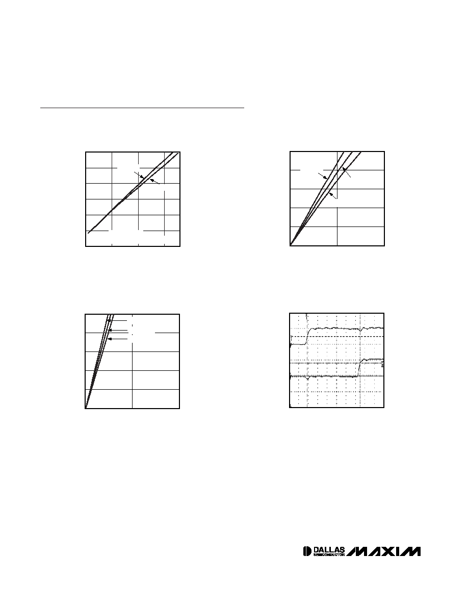
Typical Operating Characteristics
(T
A
= +25∞C, unless otherwise noted.)
DIGITAL SUPPLY CURRENT
vs. CLOCK FREQUENCY
MAXQ3212 toc01
f
HFXIN
(MHz)
I
DD1
(mA)
3
2
1
1
2
3
4
5
0
0
T
A
= -40∞C
T
A
= +85∞C
V
DD
= +5.0V
CLOCK SOURCE DRIVEN ON HFXIN
P0/P1 LOW-OUTPUT VOLTAGE
vs. SINK CURRENT
MAXQ3212 toc02
V
OL
(V)
I
OL
(mA)
1
5
10
15
20
25
0
0
2
V
DD
= +5.0V
f
HFXIN
= 3.58MHz
T
A
= -40∞C
T
A
= +85∞C
T
A
= +25∞C
P0.7 LOW-OUTPUT VOLTAGE
vs. SINK CURRENT
MAXQ3212 toc02
V
OL
(V)
I
OL
(mA)
1
5
10
15
20
25
0
0
2
V
DD
= +5.0V
f
HFXIN
= 3.58MHz
T
A
= -40∞C
T
A
= +85∞C
T
A
= +25∞C
ANALOG COMPARATOR DELAY
MAXQ3212 toc04
50ns/div
CMPI
5V/div
5V/div
CMPO
MAXQ3212
Microcontroller with Analog Comparator
and LED Driver
_____________________________________________________________________
5
Pin Description
PIN
NAME
FUNCTION
1,
13,
15
GND
Ground
2
V
REF
/P0.4
Voltage Reference Input/Output or General-Purpose, Digital I/O, Type D Port. This pin functions as either
the output of the internal voltage reference or as a bidirectional I/O. This pin can also be driven with an external
voltage to provide an optional voltage reference. The pin defaults to a digital input with a weak pullup after a
reset.
3
CMP0/P0.3
Analog Voltage Comparator Output or General-Purpose, Digital I/O, Type D Port. This pin functions as
either the output of the analog voltage comparator or as a bidirectional I/O. The pin defaults to a digital input
with a weak pullup after a reset.
4
T2P/P0.2
Timer 2 Input/Output or General-Purpose, Digital I/O, Type D Port. This pin functions as either the input or
output of Timer 2 or as a bidirectional I/O. The pin defaults to a digital input with a weak pullup after a reset.
5
T2PB/P0.1
Secondary Timer 2 Input/Output or General-Purpose, Digital I/O, Type D Port. This pin functions as either
the secondary output of Timer 2 or as a bidirectional I/O. The pin defaults to a digital input with a weak pullup
after a reset.
6
P0.0
General-Purpose, Digital I/O, Type D Port. This pin functions as a bidirectional I/O, and defaults to a digital
input with a weak pullup after a reset.
7
P1.6
General-Purpose, Digital I/O, Type D Port. This pin functions as a bidirectional I/O, and defaults to a digital
input with a weak pullup after a reset.
8
P1.5
General-Purpose, Digital I/O, Type D Port. This pin functions as a bidirectional I/O, and defaults to a digital
input with a weak pullup after a reset.
9
TDO/P1.4
D e b u g Po r t Si g n a l T D O or G e n e r a l - Pu r p o s e , Di g it a l I/ O , T y p e D Po r t . Thi s p i n functi ons as ei ther the TD O
si g nal of the d eb ug p or t or as a b i d i r ecti onal I/O . The p i n d efaul ts to a d i g i tal i np ut w i th a w eak p ul l up after a r eset.
10
TCK/P1.3
D e b u g Po r t Si g n a l T C K or Ge n e r a l - Pu r p o s e , D i g i t a l I /O , T y p e D Po r t . Thi s p i n functi ons as ei ther the TC K si g nal
of the d eb ug p or t or as a b i d i r ecti onal I/O . The p i n d efaul ts to a d i g i tal i np ut w i th a w eak p ul l up after a r eset.
11
HFXIN
Oscillator Input. Connect an external crystal or resonator between HFXIN and HFXOUT for system clock
generation. When using a crystal, a load capacitor of approximately 22pF must be connected between this pin
and ground. Alternatively, HFXIN is the input for an external clock source when HFXOUT is floating.