Features
l
Ideally Suited for Automatic Insertion
l
150
o
C Junction Temperature
l
For Switching and AF Amplifier Applications
l
Epitaxial Planar Die Construction
Mechanical Data
l
Case: SOT-23, Molded Plastic
l
Terminals: Solderable per MIL-STD-202, Method 208
l
Polarity: See Diagram
l
Weight: 0.008 grams ( approx.)
l
Marking: BC817-16 6A
BC817-25 6B
BC817-40 6C
Maximum Ratings @ 25
o
C Unless Otherwise Specified
Charateristic
Symbol Value Unit
Collector-Emitter Voltage
V
CEO
45
V
Emitter-Base Voltage
V
EBO
5
V
Collector Current
I
C
800
mA
Peak Collector Current
I
CM
1000
mA
Peak Emitter Current
I
EM
1000
mA
Power Dissipation@T
s
=50
o
C(Note1)
P
d
310
mW
Operating & Storage Temperature T
j
, T
STG
-55~150
o
C
Note:
1.
Device mounted on Ceramic Substrate 0.7mm X 2.5cm
2
area
BC817-16
THRU
BC817-40
NPN Small
Signal Transistor
310mW
www.
mccsemi
.com
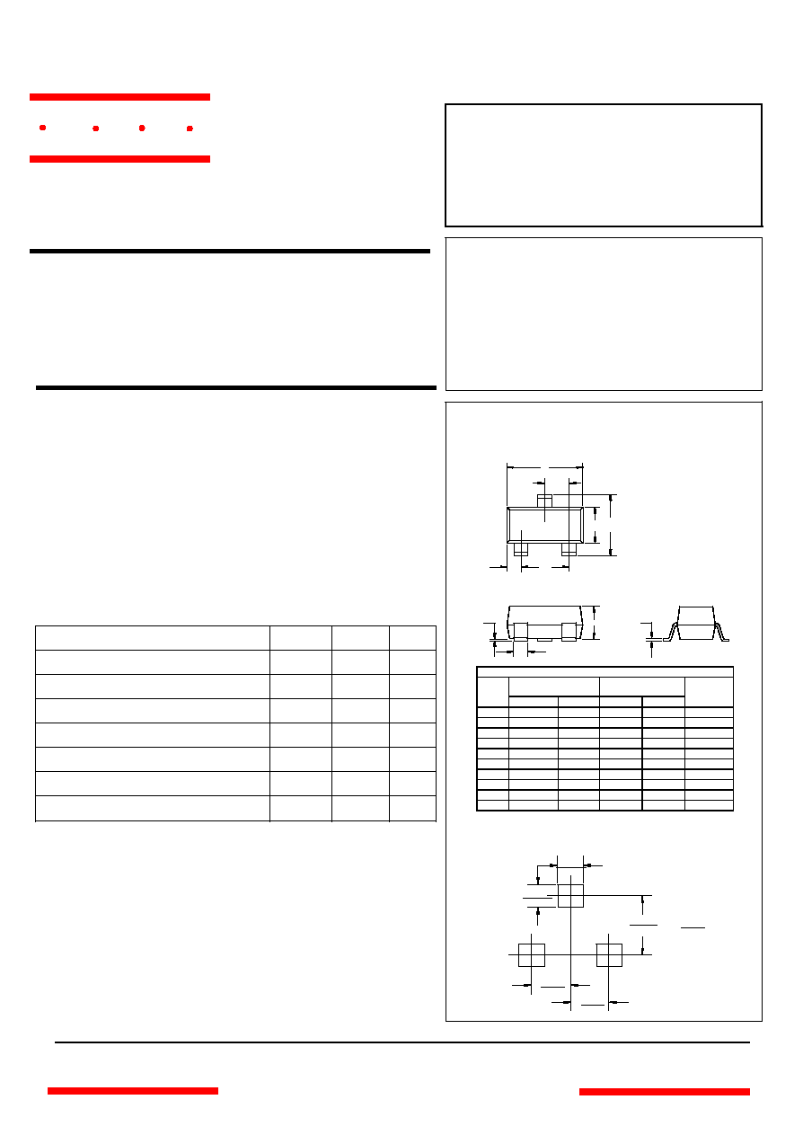
Suggested Solder
Pad Layout
DIMENSIONS
INCHES
MM
DIM
MIN
MAX
MIN
MAX
NOTE
A
.110
.120
2.80
3.04
B
.083
.098
2.10
2.64
C
.047
.055
1.20
1.40
D
.035
.041
.89
1.03
E
.070
.081
1.78
2.05
F
.018
.024
.45
.60
G
.0005
.0039
.013
.100
H
.035
.044
.89
1.12
J
.003
.007
.085
.180
K
.015
.020
.37
.51
A
B
C
D
E
F
G
H
J
.079
2.000
inches
mm
.031
.800
.035
.900
.037
.950
.037
.950
SOT-23
omponents
21201 Itasca Street Chatsworth
!"#
$
% !"#
M C C

www.
mccsemi
.com
M C C
BC817-16 thru BC817-40
Electrical Characteristics
@25∞C unless otherwise specified
Characteristic
Symbol
Min
Max
Unit
Test Condition
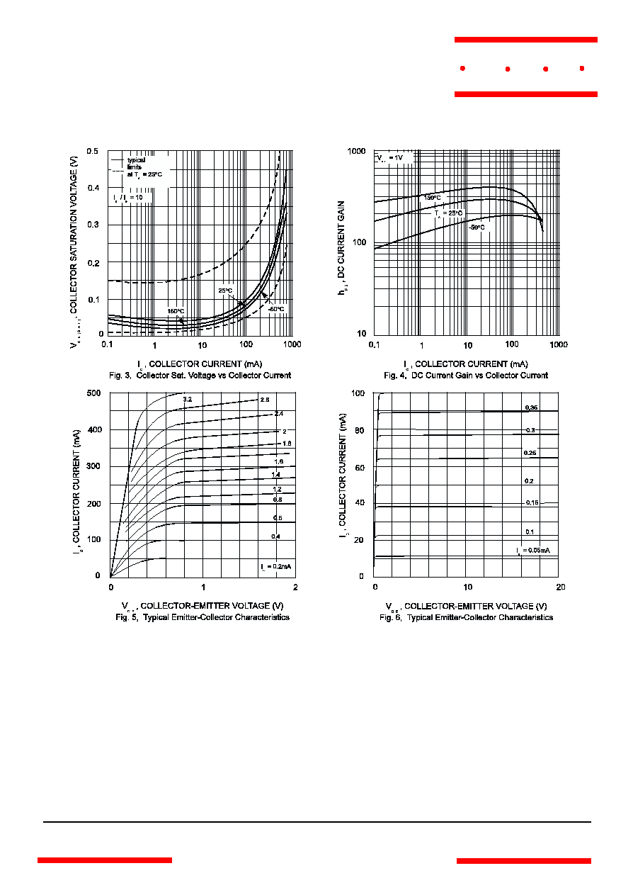
DC Current Gain
Current Gain Group -16
-25
-40
Current Gain Group -16
-25
-40
h
FE
100
160
250
60
100
170
250
400
600
--
--
--
--
V
CE
= 1.0V, I
C
= 100mA
V
CE
= 1.0V, I
C
= 300mA
Thermal Resistance, Junction to Substrate Backside
R
G
SB
--
320
K/W
Note 1
Thermal Resistance, Junction to Ambient Air
R
G
JA
--
400
K/W
Note 1
Collector-Emitter Saturation Voltage
V
CE(SAT)
--
0.7
V
I
C
= 500mA, I
B
= 50mA
Base-Emitter Voltage
V
BE
--
1.2
V
V
CE
= 1.0V, I
C
= 300mA
Collector-Emitter Cutoff Current
I
CES
--
100
5.0
nA
µA
V
CE
= 45V
V
CE
= 25V, T
j
= 150∞C
Emitter-Base Cutoff Current
I
EBO
--
100
nA
V
EB
= 4.0V
Gain Bandwidth Product
f
T
100
--
MHz
V
CE
= 5.0V, I
C
= 10mA,
f = 50MHz
Collector-Base Capacitance
C
CBO
--
12
pF
V
CB
= 10V, f = 1.0MHz