Features
l
Planar Die construction
l
500mW Power Dissipation
l
Zener Voltages from 2.4V - 39V
l
Ideally Suited for Automated Assembly Processes
Mechanical Data
l
Case: SOD-123, Molded Plastic
l
Terminals: Solderable per MIL-STD-202, Method 208
l
Approx. Weight: 0.008 grams
l
Mounting Position: Any
l
Storage & Operating Temperature: -55
o
C to +150
o
C
Maximum Ratings @ 25
o
C Unless Otherwise Specified
Zener Current I
F
100 mA
Maximum Forward
Voltage
V
F
1.2 V
Power Dissipation
(Notes A)
P
(AV)
500 mWatt
Pe ak Forward Surge I
FSM
4.0 Amps
NOTES:
MMSZ5221B
THRU
MMSZ5259B
500 mW
Zener Diodes
2.4 to 39 Volts
M C C
www.
mccsemi
.com
A. Mounted on 5.0mm2(.013mm thick) land areas.
B. Measured on 8.3ms, single half sine-wave or equivalent
Current (Notes B)
square wave, duty cycle = 4 pulses per minute maximum
.
INCHES
MM
DIM
MIN
MAX
MIN
MAX
NOTE
A .141 .154 3.60 3.90
B .098 .110 2.50 2.80
C .055 .071 1.40 1.80
D .037 .053 0.95 1.35
E .019 .028 0.50 0.70
F --- .008 --- 0.20
G .016 --- 0.40 ---
1.50
"
2.0
"
1.50
"
SUGGESTED SOLDER
PAD LAYOUT
A
B
E
C
H
D
F
G
SOD123
DIMENSIONS
omponents
21201 Itasca Street Chatsworth
!"#
$
% !"#
H --- .005 --- 0.12
MAX

www.
mccsemi
.com
NOTE:
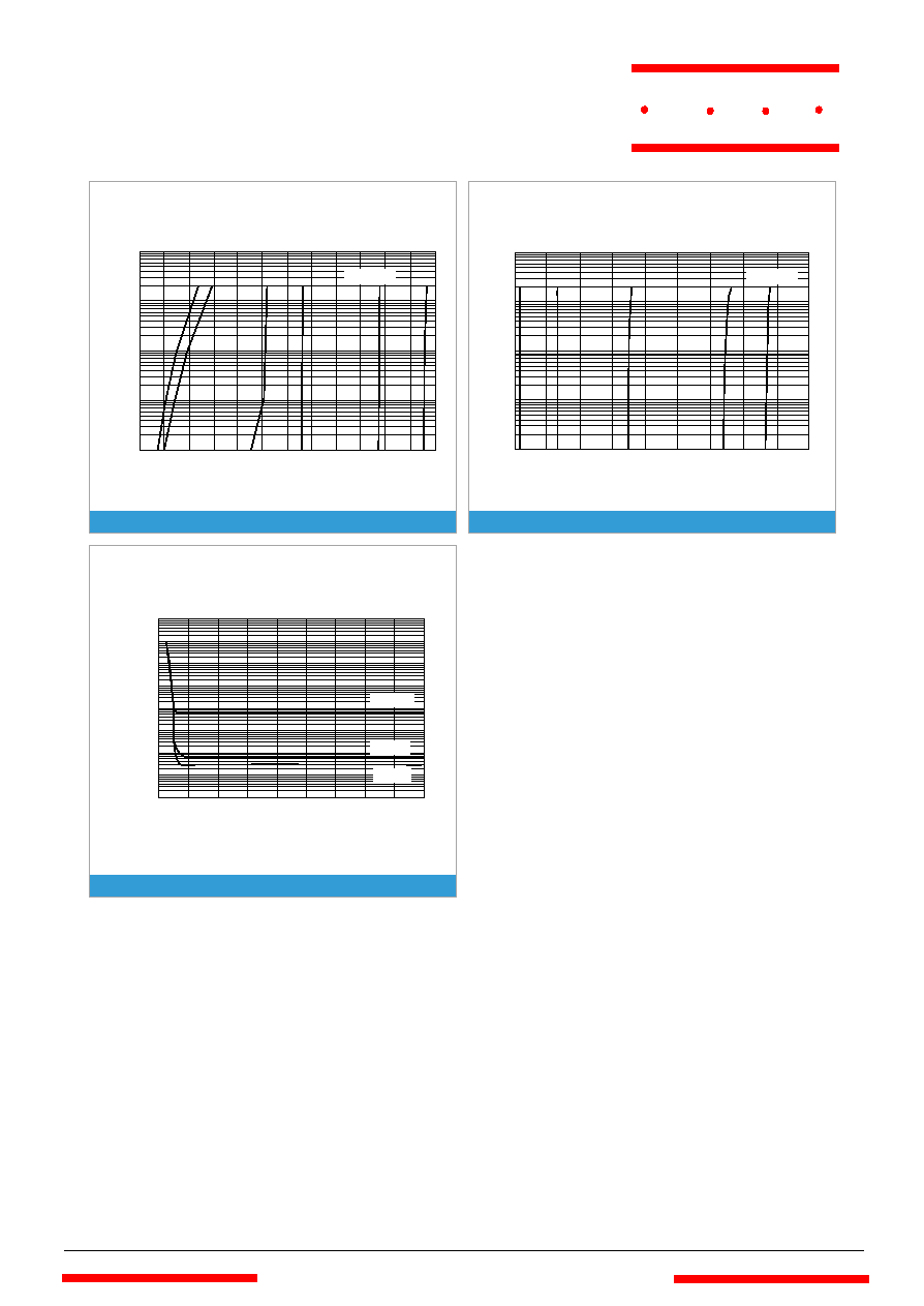
1. Tolerance and Type Number Designation. The type numbers listed have a standard tolerance on the nominal zener voltage of �5%.
2. Specials Available Include:
A. Nominal zener voltages between the voltages shown and tighter voltage tolerances.
B. Matched sets.
3. Zener Voltage (V
Z
) Measurement. Guarantees the zener voltage when measured at 90 seconds while maintaining the lead temperature (T
L
) at 30
O
C, from the diode body.
4. Zener Impedance (Z
Z
) Derivation. The zener impedance is derived from the 60 cycle ac voltage, which results when an AC current having an rms value equal to 10% of the dc zener
current (I
ZT
or I
ZK
) is superimposed on I
ZT
or I
ZK
.
5. Surge Current (I
R
) Non-Repetitive. The rating listed in the electrical characteristics table is maximum peak, non-repetitive, reverse surge current of 1/2 square wave or equivalent sine
wave pulse of 1/120 second duration superimposed on the test current, I
ZT
, per JEDEC registration; however, actual device capability is as described in Figure 5.
MMSZ5221B thru MMSZ5259B
M C C
Electrical Characteristics @ 25
o
C Unless Otherwise Specified
NORMAL
ZENER
VOLTAGE
Vz@ Izt
TEST
CURRENT Izt
MAXIMUM ZENER
IMPEDANCE
`B' SUFFIX ONLY
Zzt @ Izt Zzk @ Izk=0.25mA
MAXIMUM REVERSE
LEAKAGE CURRENT
Ir @ Vr
MAXIMUM ZENER
VOLTAGE TEMP
COEFFICIENT `B'
SUFFIX ONLY
MCC PART
NUMBER
Marking
VOLTS
mA
OHMS
OHMS
uA
VOLTS
%/
o
C
MMSZ5221B C1 2.4 20 30 1200 100 1.0 -0.085
MMSZ5222B C2 2.5 20 30 1250 100 1.0 -0.085
MMSZ5223B C3 2.7 20 30 1300 75 1.0 -0.080
MMSZ5225B C5 3.0 20 29 1600 50 1.0 -0.075
MMSZ5226B D1 3.3 20 28 1600 25 1.0 -0.070
MMSZ5227B D2 3.6 20 24 1700 15 1.0 -0.065
MMSZ5228B D3 3.9 20 23 1900 10 1.0 -0.060
MMSZ5229B D4 4.3 20 22 2000 5.0 1.0 �0.055
MMSZ5230B D5 4.7 20 19 1900 5.0 2.0 �0.030
MMSZ5231B E1 5.1 20 17 1600 5.0 2.0 �0.030
MMSZ5232B E2 5.6 20 11 1600 5.0 3.0 +0.038
MMSZ5234B E4 6.2 20 7.0 1000 5.0 4.0 +0.045
MMSZ5235B E5 6.8 20 5.0 750 3.0 5.0 +0.050
MMSZ5236B F1 7.5 20 6.0 500 3.0 6.0 +0.058
MMSZ5237B F2 8.2 20 8.0 500 3.0 6.5 +0.062
MMSZ5239B F4 9.1 20 10 600 3.0 7.0 +0.068
MMSZ5240B F5 10 20 17 600 3.0 8.0 +0.075
MMSZ5241B H1 11 20 22 600 2.0 8.4 +0.076
MMSZ5242B H2 12 20 30 600 1.0 9.1 +0.077
MMSZ5243B H3 13 9.5 13 600 0.5 9.9 +0.079
MMSZ5245B H5 15 8.5 16 600 0.1 11 +0.082
MMSZ5246B J1 16 7.8 17 600 0.1 12 +0.083
MMSZ5248B J3 18 7.0 21 600 0.1 14 +0.085
MMSZ5250B J5 20 6.2 25 600 0.1 15 +0.086
MMSZ5251B K1 22 5.6 29 600 0.1 17 +0.087
MMSZ5252B K2 24 5.2 33 600 0.1 18 +0.088
MMSZ5254B K4 27 4.6 41 600 0.1 21 +0.090
MMSZ5255B K5 28 4.5 44 600 0.1 21 +0.091
MMSZ5256B M1 30 4.2 49 600 0.1 23 +0.091
MMSZ5257B M2 33 3.8 58 700 0.1 25 +0.092
MMSZ5258B M3 36 3.4 70 700 0.1 27 +0.093
MMSZ5259B M4 39 3.2 80 800 0.1 30 +0.094
MMSZ5221B thru MMSZ5259B
www.
mccsemi
.com
M C C
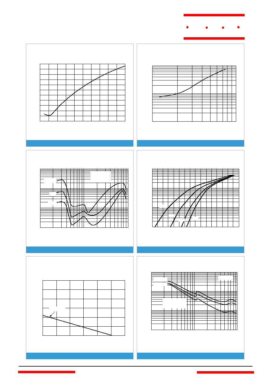
TYPICAL REVERSE CURRENT
TEMPERA
TURE
COEFFICIENT
,mV
/
C
)
o
NOMINAL ZENER VOLTAGE, Volts
-1
0
1
2
3
4
5
6
7
8
12
11
10
9
8
7
6
5
4
3
2
-2
-3
STEADY STATE POWER DERATING
EFFECT OF ZENER VOLTAGE ON ZENER IMPEDANCE
100
10
1
1000
100
10
1
IZ = 1 mA
5 mA
20 mA
DYNAMIC
I
MPEDANCE,
W
NORMAL ZENER VOLTAGE, Volts
T
J
=25 C
O
I
Z(AC)=0.1
I
F=1 kHZ
Z(DC)
FOR
W
ARD
CURRENT
,m
A
TYPICAL FORWARD VOLTAGE
FORWARD VOLTAGE, Volts
1.2
1.1
1.0
0.9
0.8
0.7
0.6
0.5
0.4
1000
100
10
1
75 C
O
5 C
O
25 C
O
150 C
O
TYPICAL CAPACITANCE
100
1000
100
10
1
10
1
BIAS AT
50% OF VZ NOM
0 V BIAS
1 V BIAS
CAP
ACIT
ANCE,
pF
NOMINAL ZENER VOLTAGE, Volts
T =25 C
A
o
100
10
1
NOMINAL ZENER VOLTAGE, Volts
TEMPERA
TURE
COEFFICIENT
,mV
/
C
)
o
10
100
TEMPERATURE ( C)
o
POWER
DISSIP
A
TION,
W
atts
STEADY STATE POWER DERATING
1.2
1.0
0.8
0.6
0.4
0.2
0
150
125
100
75
50
25
P
D V
.
S
. T
A
155