Transient Voltage
Protection Device
65 Volts
Features
∑
Oxide-Glass passivated Junction
∑
Bi-Directional protection in a single device
∑
Surge capabilities up to 50A@10/1000us or 150A@8/20us
∑
High Off-State impedance and Low On-State voltage
∑
Plastic material has UL flammability classification 94V -0
Mechanical Data
∑
Case : Molded plastic
∑
Polarity : None cathode band denotes
∑
Approx Weight : 0.093grams
Maximum Ratings
Characteristic Symbol Value Unit
Non-repetitive peak
impulse current I
PP
50A 10/1000us
Non-repetitive peak
On-state current I
TSM
20A
8.3ms, one-half
cycle
Operating temperature
range T
OP
-40~125
o
C
Junction and storage
temperature range
T
J
, T
STG
-55~150
o
C
Thermal Resistance
Characteristic Symbol Value Unit
Thermal Resistance
junction to lead
30
o
C/W
Thermal Resistance
junction to ambient 120
o
C/W On recommended
pad layout
Typical positive
temperature
coefficient for
breakdown voltage
0.1%/
o
C
V
BR
/
T
J
www.
mccsemi
.com
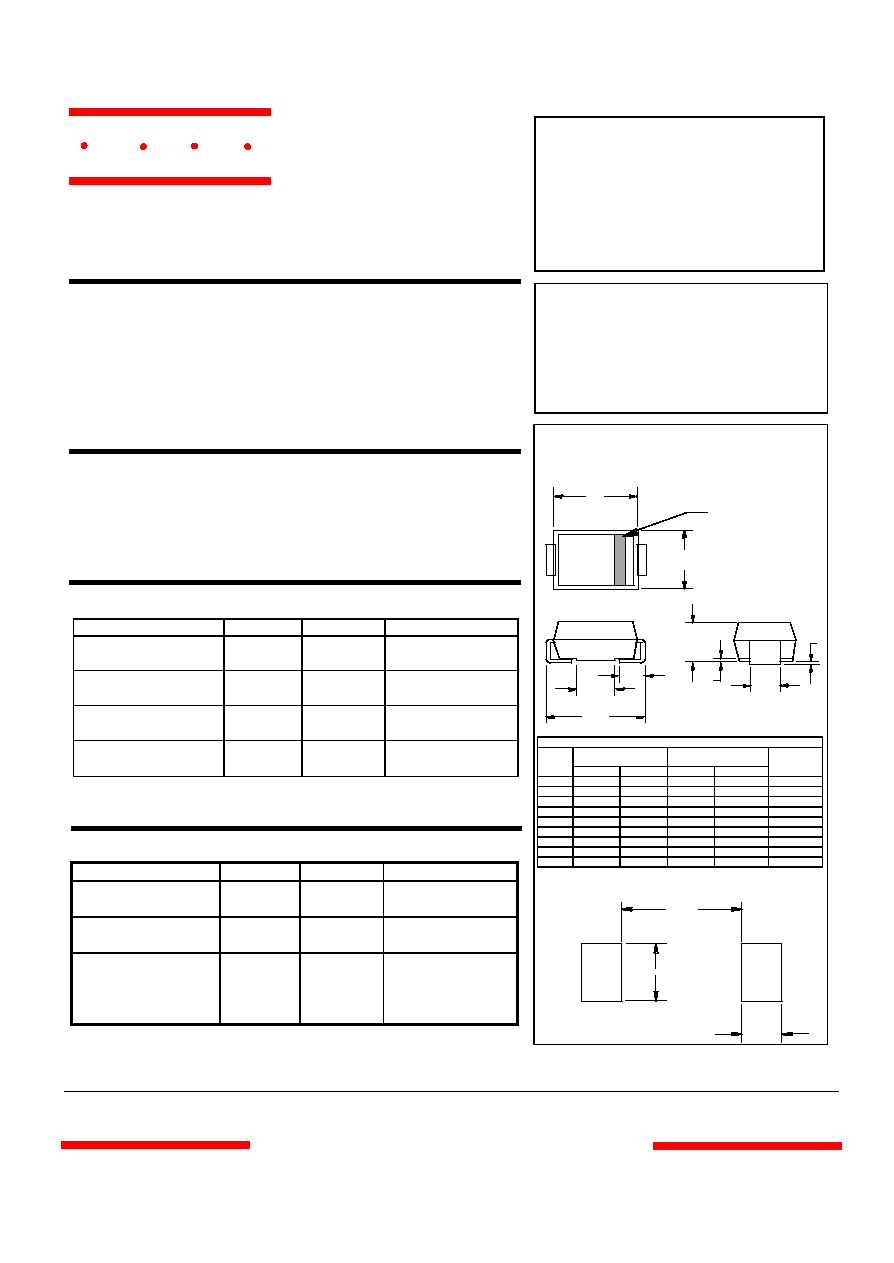
DO-214AA
(SMBJ)
H
J
E
F
G
A
B
D
C
Cathode Band
DIMENSIONS
INCHES MM
DIM MIN MAX MIN MAX NOTE
A .078 .096 2.00 2.44
B .077 .083 1.96 2.10
C .002 .008 .05 .20
D --- .02 --- .51
E .030 .060 .76 1.52
F .065 .091 1.65 2.32
G .205 .220 5.21 5.59
H .160 .180 4.06 4.57
J .130 .155 3.30 3.94
0.070"
0.090"
0.085"
SUGGESTED SOLDER
PAD LAYOUT
TSMBJ0305C-072
R
q
JA
R
q
J
L
omponents
21201 Itasca Street Chatsworth
!"#
$
% !"#
M C C
www.
mccsemi
.com
M C C
Parameter
Rated
Repetitive Off
-state Voltage
Off-state
Leakage
Current@V
DRM
Breakover
Voltage
On-State
Voltage
@I
T
=1.0A
Breakover Current Holding Current
Off-State
Capacitance
Symbol
V
DRM
I
DRM
V
BO
V
T
I
BO-
I
BO+
I
H-
I
H+
C
J
Units
Volts
uA
Volts
Volts
mA
mA
mA
mA
pF
Limit
Max
Max
Max
Max
Min
Max
Min
Max
Typ.
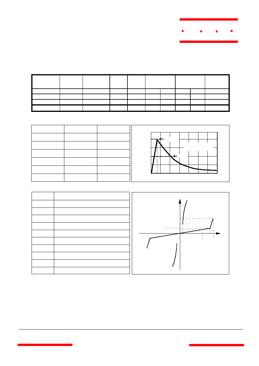
MAXIMUM RATED SURGE WAVEFORM
MAXIMUM RATED SURGE WAVEFORM
MAXIMUM RATED SURGE WAVEFORM
MAXIMUM RATED SURGE WAVEFORM
Waveform
Standard
Ipp (A)
2/10 us
GR-1089-CORE
200
8/20 us
IEC 61000-4-5
150
10/160 us
FCC Part 68
1
00
10/700 us
ITU-T K20/21
60
10/560 us
FCC Part 68
6
0
10/1000 us
GR-1089-CORE
50
TIME
0
50
100
0
Ipp ; PEAK PULSE CURRENT (%)
Peak value (Ipp)
Half value
tr
tp
tr = rise time to peak value
tp = decay time to half value
Symbol
Parameter
V
DRM
Stand-off voltage
I
DRM
Leakage current at stand-off voltage
V
BR
Breakdown voltage
I
BR
Breakdown current
V
BO
Breakover voltage
I
BO
Breakover current
I
H
Holding current
NOTE: 1
V
T
On state voltage
I
PP
Peak pulse current
C
O
Off-state capacitance
NOTE: 2
I
V
V
DRM
I
PP
I
BO
I
H
I
BR
I
DRM
V
BR
V
BO
V
T
NOTE
1. I H > ( V L/ R L
)
If this criterion is not obeyed, the TSPD triggers but does not return correctly to high-resistance state.
The surge recovery time. It does not exceed 30ms.
2. Off-state capacitance measured at f=1.0MHz , 1.0Vrms signal , VR=2Vdc bias.
ELECTRICAL CHARACTERISTIC
@25
Unless otherwise specified
TSMBJ0305C-072
TSMBJ0305C-072 65 5 88 5 50 800 150 800 100

M C C
TSMBJ0305C-072
-50
-25
0
25
50
75
100
125
150
175
Tj ; JUNCTION TEMPERATURE (
)
0.9
0.95
1
1.05
1.1
1.15
1.2
NORMALISED BREAKDOWN VOLTAGE
Fig.2 - Relative Variation of
Breakdown Voltage v.s Junction Temperature
-25
0
25
50
75
100
125
150
Tj , JUNCTION TEMPERATURE (
)
0.001
0.01
0.1
1
10
100
I(DRM) , OFF-STATE CURRENT(uA)
Fig.1 - Off-State Current v.s Junction Temperature
V
DRM
= 50V
V
BR
(T
J
)
V
BR
(T
J
=25
)
-50
-25
0
25
50
75
100
125
150
175
Tj ; JUNCTION TEMPERATURE (
)
0.95
1
1.05
1.1
NORMALISED BREAKOVER VOLTAGE
Fig.3 - Relative Variation of
Breakover Voltage v.s Junction Temperature
V
BO
(T
J
)
V
BO
(T
J
=25
)
1
2
3
4
5
6
7
8
9
V(T) ; ON-STATE VOLTAGE
1
10
100
I(T) ; ON-STATE CURRENT (A)
Fig.4 - On-State Current v.s On-State Voltage
T
J
= 25
-50
-25
0
25
50
75
100
125
Tj ; JUNCTION TEMPERATURE (
)
0
0.5
1
1.5
2
NORMALISED HOLDING CURRENT
Fig.5 - Relative Variation of
Holding Current v.s Junction Temperature
I
H
(T
J
)
I
H
(T
J
=25
)
1
10
100
VR ; REVERSE VOLTAGE (V)
0.1
1
NORMALISED CAPACITANCE
Fig.6 - Relative Variation of
Junction Capacitance v.s Reverse Voltage Bias
Tj =25
f=1MHz
V
RMS
= 1V
C
O
(VR)
C
O
(VR = 1V)
www.
mccsemi
.com

M C C
www.
mccsemi
.com
TELECOM
EQUIPMENT
E.G. MODEM
TIP
RING
FUSE
FUSE
FUSE
FUSE
TSPD 1
TSPD 1
TSPD 1
TSPD 1
TELECOM
EQUIPMENT
E.G. ISDN
TIP
RING
TSPD 1
TSPD 1
TSPD 1
TSPD 1
TSPD 2
TSPD 2
TSPD 2
TSPD 2
PTC
PTC
TELECOM
EQUIPMENT
E.G. LINE CARD
TIP
RING
TSPD 2
TSPD 2
TSPD 2
TSPD 2
TSPD 3
TSPD 3
TSPD 3
TSPD 3
TSPD 1
TSPD 1
TSPD 1
TSPD 1
PTC
PTC
TYPICAL APPLICATION CIRCUITS
The PTC (Positive Temperature Coefficient) is an overcurrent protection device.
TSMBJ0305C-072