1
MX23L12854
128M-BIT Low Voltage, Serial Mask ROM Memory with
50MHz SPI Bus Interface
FEATURES
∑
128Mbit of Mask ROM
∑
3.0 to 3.6V Single Supply Voltage
∑
SPI Bus Compatible Serial Interface
∑
50MHz Clock Rate (maximum)
DESCRIPTION
The MX23L12854 is a 128Mbit (16M x 8) Serial Mask ROM
accessed by a high speed SPI-compatible bus.
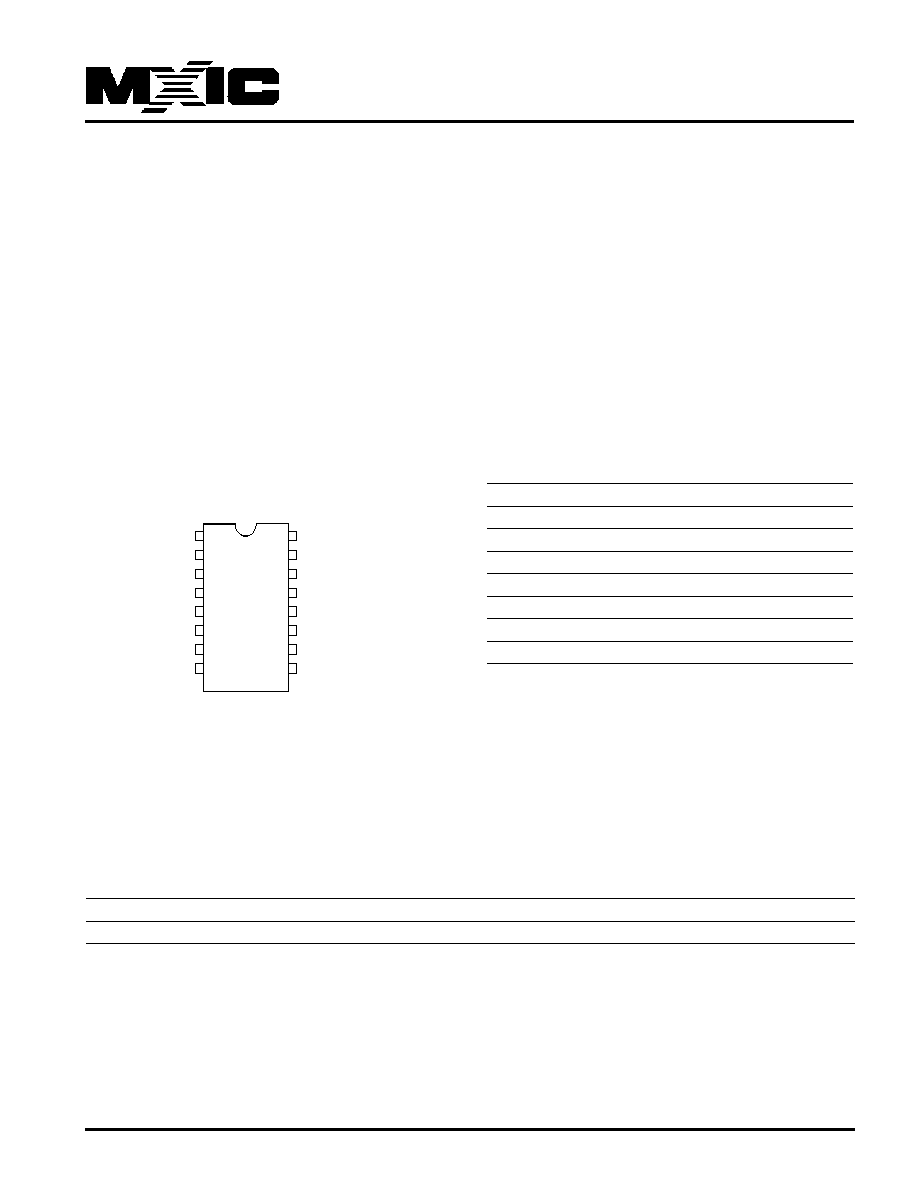
PIN CONFIGURATIONS
SYMBOL
DESCRIPTION
C
Serial Clock
D
Serial Data Input
Q
Serial Data Output
S#
Chip Select
HOLD#
Hold
VCC
Supply Voltage
VSS
Ground
PIN DESCRIPTION
16-PIN SOP (300 mil)
1
2
3
4
5
6
7
8
HOLD#
VCC
NC
NC
NC
NC
S#
Q
16
15
14
13
12
11
10
9
C
D
NC
NC
NC
NC
VSS
NC
Note:
1. NC=No Connection
2. See page 16 (onwards) for package dimensions, and
how to identify pin-1.
P/N: PM1141
REV. 1.1, MAY. 04, 2005
ORDER INFORMATION
Part No.
Speed
Package
Remark
MX23L12854MC-20G
20ns
16-SOP
Pb-free
2
P/N: PM1141
REV. 1.1, MAY. 04, 2005
MX23L12854
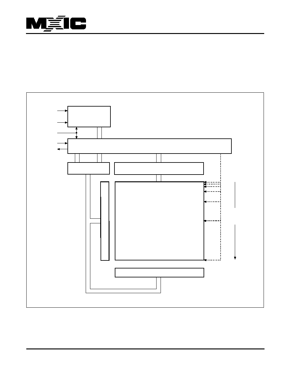
MEMORY ORGANIZATION
The memory is organized as:
- 16M bytes (8 bits each)
BLOCK DIAGRAM
HOLD#
S#
Control Logic
I/O Shift Register
Address Register
and Counter
512 Byte
Data Buffer
X Decoder
Y Decoder
Size of the
read-only
memory area
C
D
Q

3
P/N: PM1141
REV. 1.1, MAY. 04, 2005
MX23L12854
SIGNAL DESCRIPTION
Serial Data Output (Q). This output signal is used to
transfer data serially out of the device. Data is shifted out
on the falling edge of Serial Clock (C).
Serial Data Input (D). This input signal is used to transfer
data serially into the device. It receives instructions,
addresses, and the data to be programmed. Values are
latched on the rising edge of Serial Clock (C).
Serial Clock (C). This input signal provides the timing of
the serial interface. Instructions, addresses, or data
present at Serial Data Input (D) are latched on the rising
edge of Serial Clock (C). Data on Serial Data Output (Q)
changes after the falling edge of Serial Clock (C).
Chip Select (S#). When this input signal is High, the
device is deselected. Driving Chip Select (S#) Low ena-
bles the device, placing it in the active power mode.
After Power-up, a falling edge on Chip Select (S#) is
required prior to the start of any instruction.
Hold (HOLD#). The Hold (HOLD#) signal is used to pause
any serial communications with the device without
deselecting the device.
During the Hold condition, the Serial Data Output (Q) is high
impedance, and Serial Data Input (D) and Serial Clock (C)
are Don't Care.
To start the Hold condition, the device must be selected,
with Chip Select (S#) driven Low.
4
P/N: PM1141
REV. 1.1, MAY. 04, 2005
MX23L12854
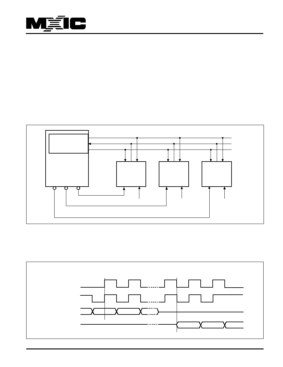
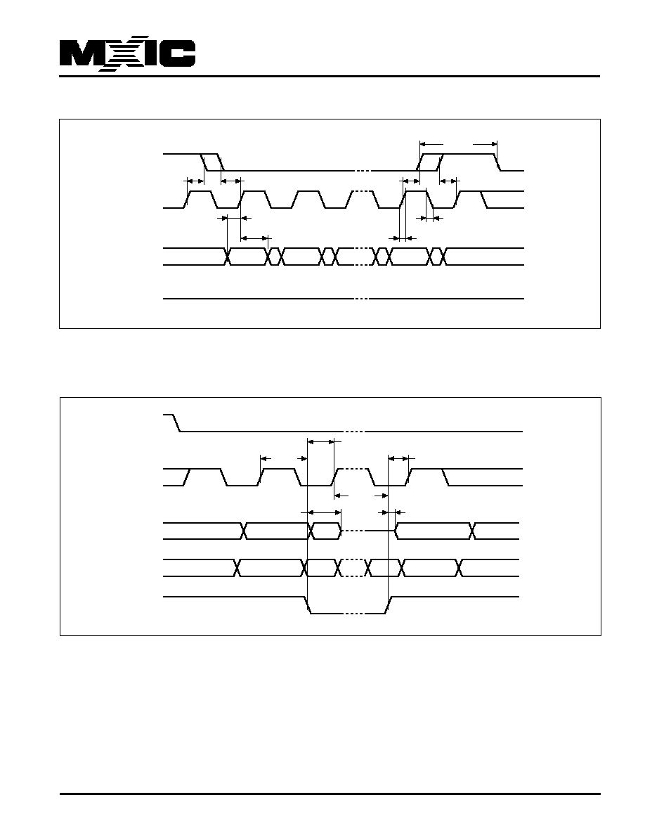
SPI MODES
These devices can be driven by a microcontroller with its
SPI peripheral running in either of the two following modes:
- CPOL=0, CPHA=0
- CPOL=1, CPHA=1
For these two modes, input data is latched in on the rising
edge of Serial Clock (C), and output data is available from
the falling edge of Serial Clock (C).
The difference between the two modes, as shown in Figure
2, is the clock polarity when the bus master is in Stand-by
mode and not transferring data:
- C remains at 0 for (CPOL=0, CPHA=0)
- C remains at 1 for (CPOL=1, CPHA=1)
Figure 1. Bus Master and Memory Devices on the SPI Bus
Note: 1. Hold (HOLD#) signals should be driven, High or Low as appropriate.
Figure 2. SPI Modes Supported
Bus Master
(ST6, ST7, ST9,
ST10, Others)
SPI Memory
Device
SDO
SDI
SCK
C
Q
D
SPI Memory
Device
C
Q
D
SPI Memory
Device
C
Q
D
S#
CS3
CS2
CS1
SPI Interface with
(CPOL, CPHA) =
(0, 0) or (1, 1)
HOLD#
S#
HOLD#
S#
HOLD#
C
MSB
CPHA
D
0
1
CPOL
0
1
Q
C
MSB
5
P/N: PM1141
REV. 1.1, MAY. 04, 2005
MX23L12854
OPERATING FEATURES
Active Power, Stand-by Power
When Chip Select (S#) is Low, the device is enabled, and
in the Active Power mode. When Chip Select (S#) is High,
the device is disabled, but could remain in the Active
Power mode until all internal cycles have completed. The
device then goes in to the Stand-by Power mode. The
device consumption drops to ICC1 .
Protection Modes
The environments where non-volatile memory devices are
used can be very noisy. No SPI device can operate
correctly in the presence of excessive noise. To help
combat this, the MX23L12854 boasts the following data
protection mechanisms:
- Power-On Reset and an internal timer (tPUW) can provide
protection against inadvertant changes while the power
supply is outside the operating specification.
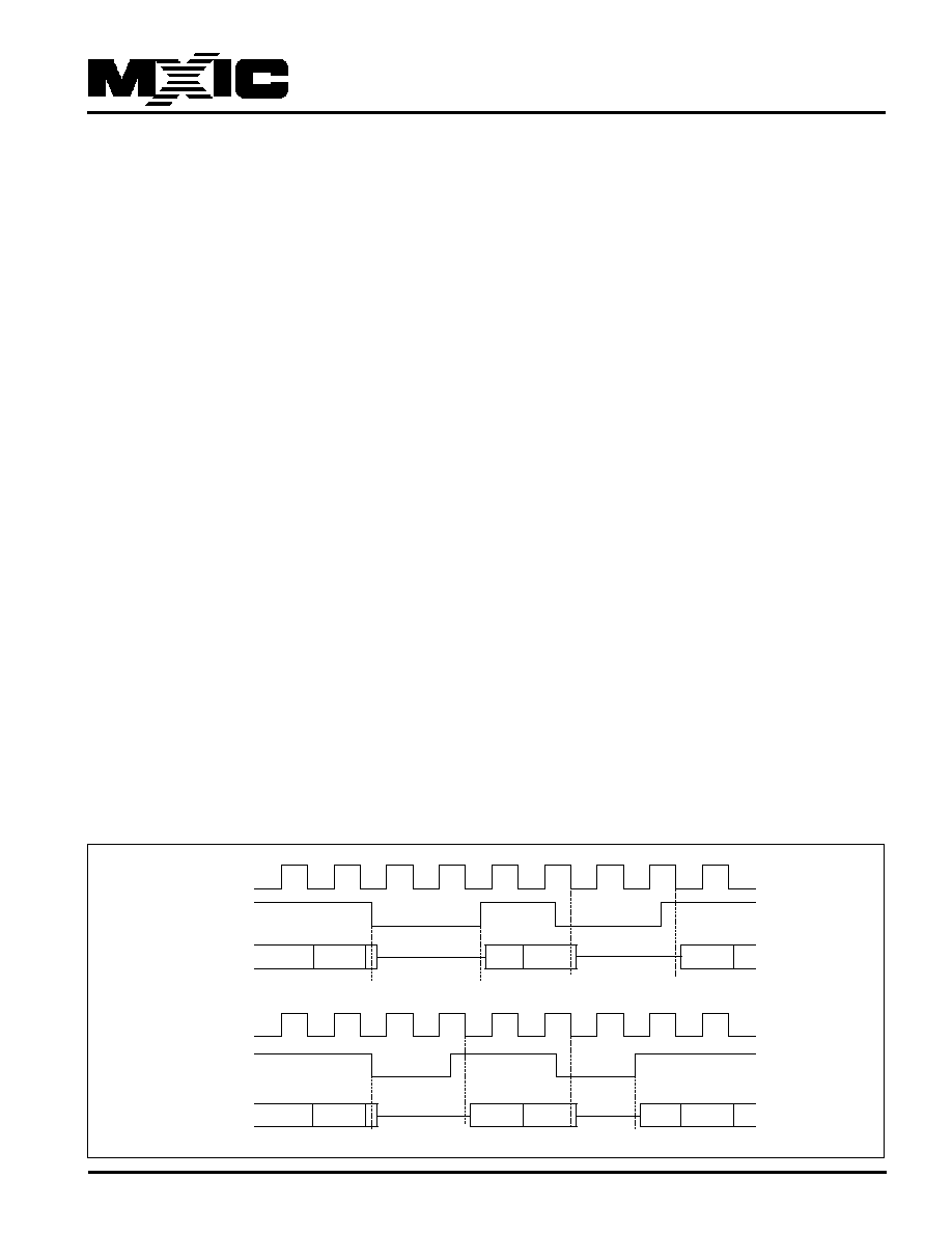
Hold Condition
The Hold (HOLD#) signal is used to pause any serial
communications with the device without resetting the
clocking sequence.
To enter the Hold condition, the device must be selected,
with Chip Select (S#) Low.
The Hold condition starts on the falling edge of the Hold
(HOLD) signal, provided that this coincides with Serial
Clock (C) being Low (as shown in Figure 3).
The Hold condition ends on the rising edge of the Hold
(HOLD#) signal, provided that this coincides with Serial
Clock (C) being Low.
If the falling edge does not coincide with Serial Clock (C)
being Low, the Hold condition starts after Serial Clock (C)
next goes Low. Similarly, if the rising edge does not
coincide with Serial Clock (C) being Low, the Hold condi-
tion ends after Serial Clock (C) next goes Low. (This is
shown in Figure 2).
During the Hold condition, the Serial Data Output (Q) is
high impedance, and Serial Data Input (D) and Serial Clock
(C) are Don't Care.
Normally, the device is kept selected, with Chip Select
(S#) driven Low, for the whole duration of the Hold condi-
tion. This is to ensure that the state of the internal logic
remains unchanged from the moment of entering the Hold
condition.
If Chip Select (S#) goes High while the device is in the Hold
condition, this has the effect of resetting the internal logic
of the device. To restart communication with the device,
it is necessary to drive Hold (HOLD#) High, and then to
drive Chip Select (S#) Low. This prevents the device from
going back to the Hold condition.
Figure 3. Hold Condition Activation (for data output only)
Q4
Q2
Q1
Q0
Q
C
HOLD#
HOLD#
C
Q0
Q1
Q3
Q4
Q5
Q2
Q2
Q3
Q2
Q5
Q6
Q

6
P/N: PM1141
REV. 1.1, MAY. 04, 2005
MX23L12854
INSTRUCTIONS
All instructions, addresses and data are shifted in and out
of the device, most significant bit first.
Serial Data Input (D) is sampled on the first rising edge of
Serial Clock (C) after Chip Select (S#) is driven Low. Then,
the one-byte instruction code must be shifted in to the
device, most significant bit first, on Serial Data Input (D),
each bit being latched on the rising edges of Serial Clock
(C).
The instruction set is listed in Table 1.
Table 1. Instruction Set
Every instruction sequence starts with a one-byte instruc-
tion code. Depending on the instruction, this might be
followed by address bytes, or by data bytes, or by both or
none.
In the case of a Read Data Bytes (READ), Read Data
Bytes at Higher Speed (Fast_Read), the shifted-in instruc-
tion sequence is followed by a data-out sequence. Chip
Select (S#) can be driven High after any bit of the data-out
sequence is being shifted out.
Instruction
Description
One-byte Instruction Code
Address
Bytes
Dummy
Bytes
Data
Bytes
READ
Read Data Bytes
0000 0011
03h
3
0
1 to
FAST_READ Read Data Bytes at Higher Speed
0000 1011
0Bh
3
1
1 to
7
P/N: PM1141
REV. 1.1, MAY. 04, 2005
MX23L12854
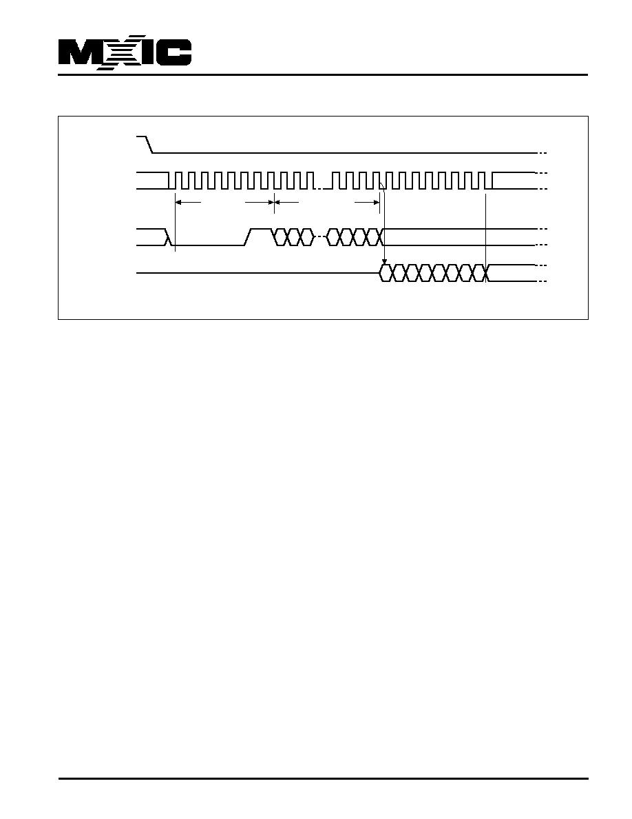
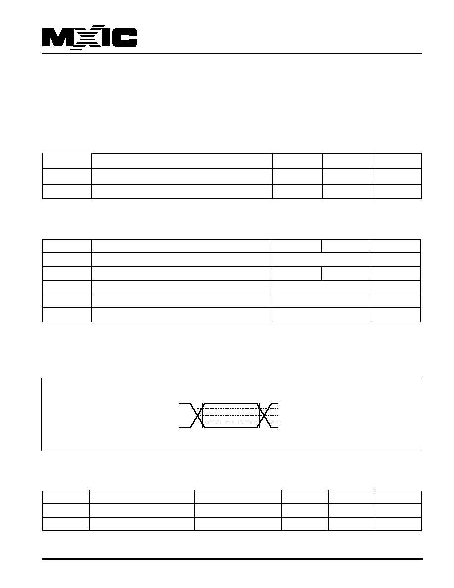
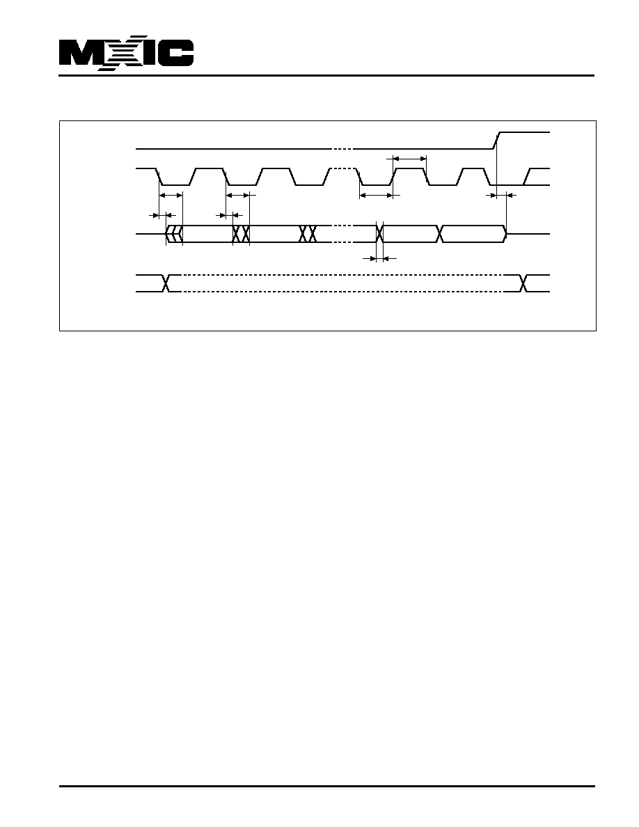
Figure 4. Read Data Bytes (READ) Instruction Sequence and Data-Out Sequence
Read Data Bytes (READ)
The device is first selected by driving Chip Select (S#) Low.
The instruction code for the Read Data Bytes (READ)
instruction is followed by a 3-byte address (A23-A0), each
bit being latched-in during the rising edge of Serial Clock
(C). Then the memory contents, at that address, is shifted
out on Serial Data Output (Q), each bit being shifted out, at
a maximum frequency fR, during the falling edge of Serial
Clock (C).
The instruction sequence is shown in Figure 4. The first
byte addressed can be at any location. The address is
automatically incremented to the next higher address after
each byte of data is shifted out. The whole memory can,
therefore, be read with a single Read Data Bytes (READ)
instruction.When the highest address is reached, the
address counter rolls over to 000000h, allowing the read
sequence to be continued indefinitely.
The Read Data Bytes (READ) instruction is terminated by
driving Chip Select (S#) High. Chip Select (S#) can be
driven High at any time during data output.
C
D
S#
Q
23
2
1
3
4
5
6
7
8
9 10
28 29 30 31 32 33 34 35
22 21
3
2
1
0
36 37 38
7
6
5
4
3
1
7
0
High Impedance
Data Out 1
Instruction
24-Bit Address
0
MSB
MSB
2
39
Data Out 2
8
P/N: PM1141
REV. 1.1, MAY. 04, 2005
MX23L12854
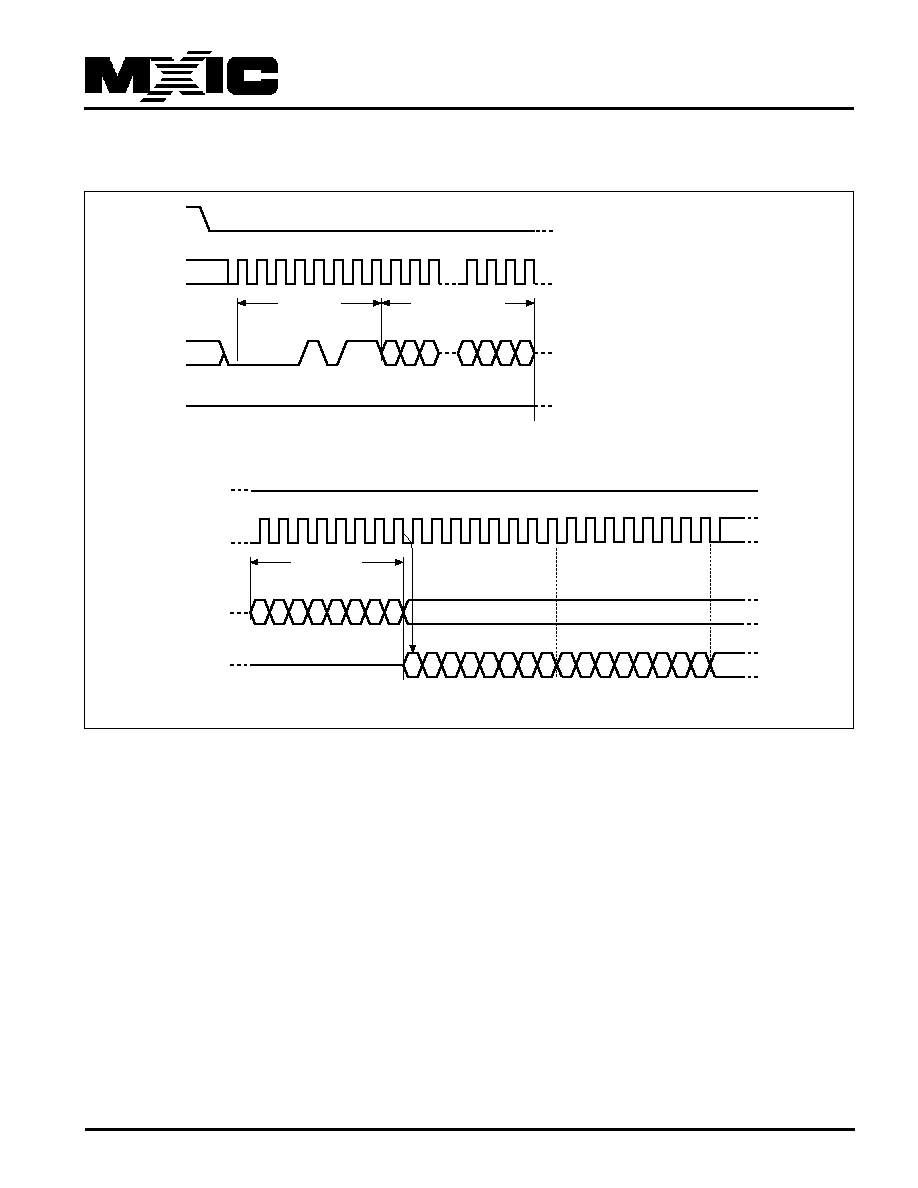
Figure 5. Read Data Bytes at Higher Speed (FAST_READ) Instruction Sequence and Data-Out
Sequence
23
2
1
3
4
5
6
7
8
9 10
28 29 30 31
22 21
3
2
1
0
High Impedance
Instruction
24 BIT ADDRESS
0
32 33 34
36 37 38 39 40 41 42 43 44 45 46
7
6
5
4
3
2
0
1
DATA OUT 1
Dummy Byte
MSB
7
6
5
4
3
2
1
0
DATA OUT 2
MSB
MSB
7
47
7
6
5
4
3
2
0
1
35
C
D
S#
Q
C
D
S#
Q
Read Data Bytes at Higher Speed (FAST_READ)
The device is first selected by driving Chip Select (S#)
Low. The instruction code for the Read Data Bytes at
Higher Speed (FAST_READ) instruction is followed by a 3-
byte address (A23-A0) and a dummy byte, each bit being
latched-in during the rising edge of Serial Clock (C). Then
the memory contents, at that address, is shifted out on
Serial Data Output (Q), each bit being shifted out, at a
maximum frequency fC, during the falling edge of Serial
Clock (C).
The instruction sequence is shown in Figure 5. The first
byte addressed can be at any location. The address is
automatically incremented to the next higher address after
each byte of data is shifted out. The whole memory can,
therefore, be read with a single Read Data Bytes at Higher
Speed (FAST_READ) instruction. When the highest ad-
dress is reached, the address counter rolls over to 000000h,
allowing the read sequence to be continued indefinitely.
The Read Data Bytes at Higher Speed (FAST_READ)
instruction is terminated by driving Chip Select (S#) High.
Chip Select (S#) can be driven High at any time during data
output.
9
P/N: PM1141
REV. 1.1, MAY. 04, 2005
MX23L12854
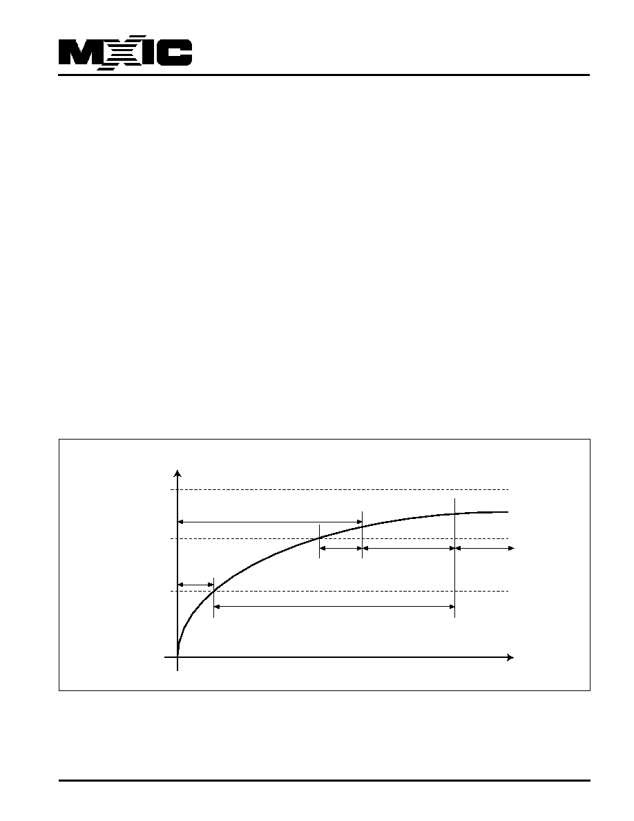
POWER-UP AND POWER-DOWN
At Power-up and Power-down, the device must not be
selected (that is Chip Select (S#) must follow the voltage
applied on VCC ) until VCC reaches the correct value:
- VCC(min) at Power-up, and then for a further delay of
tVSL
- VSS at Power-down
Usually a simple pull-up resistor on Chip Select (S#) can
be used to insure safe and proper Power-up and Power-
down.
To avoid data corruption and inadvertent write operations
during power up, a Power On Reset (POR) circuit is
included. The logic inside the device is held reset while
VCC is less than the POR threshold value, VWI -- all
operations are disabled, and the device does not respond
to any instruction.
These values are specified in Table 2.
Figure 6. Power-up Timing
If the delay, tVSL, has elapsed, after VCC has risen
above VCC (min), the device can be selected for READ
instructions even if the tPUW delay is not yet fully
elapsed.
At Power-up, the device is in the following state:
- The device is in the Standby mode.
Normal precautions must be taken for supply rail
decoupling, to stablise the VCC feed. Each device in a
system should have the VCC rail decoupled by a suitable
capacitor close to the package pins.
(Generally, this capacitor is of the order of 0.1uF).
At Power-down, when VCC drops from the operating
voltage, to below the POR threshold value, VWI , all
operations are disabled and the device does not respond
to any instruction.
VCC
VCC(min)
VWI
Reset State
of the
Device
Chip Selection Not Allowed
tVSL
tPUW
time
Read Access allowed
Device fully
accessible
VCC(max)
10
P/N: PM1141
REV. 1.1, MAY. 04, 2005
MX23L12854
Table 2. Power-Up Timing
MAXIMUM RATING
Stressing the device above the rating listed in the"Absolute
Maximum Ratings" table may cause permanent damage to
the device. These are stress ratings only and operation of
the device at these or any other conditions above those
indicated in the Operating sections of this specification is
not implied. Exposure to Absolute Maximum Rating con-
ditions for extended periods may affect device reliability.
Table 3. Absolute Maximum Ratings
Note: 1. Compliant with the ECOPACK
Æ
7191395 specifiication for lead-free soldering processes
2. Not exceeding 250∞C for more than 30 seconds, and peaking at 260∞C
3. JEDEC Std JESD22-A114A (C1=100 pF, R1=1500
, R2=500
)
Symbol
Parameter
Min.
Max.
Unit
T
STG
Storage Temperature
- 65
150
∞C
T
LEAD
Lead Temperature during Soldering
1
260
2
∞C
V
IO
Input and Output Voltage (with respect to Ground)
V
CC
Supply Voltage
V
ESD
Electrostatic Discharge Voltage (Human Body model)
3
- 2000
2000
V
- 0.6
4.0
V
- 0.6
4.0
V
Note: 1. These parameters are characterized only.
Symbol
Parameter
Min.
Max.
Unit
t
VSL
1
V
CC
(min) to S# low
30
us
11
P/N: PM1141
REV. 1.1, MAY. 04, 2005
MX23L12854
DC AND AC PARAMETERS
This section summarizes the operating and mea-surement
conditions, and the DC and AC characteristics of the
device. The parameters in the DC and AC Characteristic
Table 4. Operating Conditions
Table 5. AC Measurement Conditions
Note: 1. Output Hi-Z is defined as the point where data out is no longer driven.
Symbol
Parameter
Min.
Max.
Unit
C
L
Load Capacitance
30
pF
Input Rise and Fall Times
5
ns
Input Pulse Voltages
0.2V
CC
to 0.8V
CC
V
Input Timing Reference Voltages
0.3V
CC
to 0.7V
CC
V
Output Timing Reference Voltages
V
CC
/ 2
V
Figure 7. AC Measurement I/O Waveform
0.8VCC
0.2VCC
0.7VCC
0.3VCC
Input and Output
Timing Reference Levels
Input Levels
0.5VCC
Table 6. Capacitance
tables that follow are derived from tests performed under
the Measurement Conditions summarized in the relevant
tables. Designers should check that the operating condi-
tions in their circuit match the measurement conditions
when relying on the quoted parameters.
Note: Sampled only, not 100% tested, at T
A
=25∞C and a frequency of 20 MHz.
Symbol
Parameter
Test Condition
Min
.
Max
.
Unit
C
OUT
Output Capacitance (Q)
V
OUT
= 0V
8
pF
C
IN
Input Capacitance (other pins)
V
IN
= 0V
6
pF
Symbol
Parameter
Min.
Max.
Unit
V
CC
Supply Voltage
T
A
Ambient Operating Temperature
- 40
85
∞C
3.0
3.6
V

12
P/N: PM1141
REV. 1.1, MAY. 04, 2005
MX23L12854
Table 7. DC Characteristics
Symbol
Parameter
Test Condition
(in addition to those in Table 8)
Min.
Max.
Unit
I
LI
Input Leakage Current
± 2
uA
I
LO
Output Leakage Current
± 2
uA
I
CC1
Standby Current
S # = V
CC
, V
IN
= V
SS
or
V
CC
50
uA
I
CC2
Operating Current (READ)
C = 0.1V
CC
/ 0.9.V
CC
at 50MHz,
Q = open
8
mA
C = 0.1V
CC
/ 0.9.V
CC
at 20MHz,
Q = open
4
mA
V
IL
Input Low Voltage
- 0.5
0.3V
CC
V
V
IH
Input High Voltage
0.7V
CC
V
CC
+0.4
V
V
OL
Output Low Voltage
I
OL
= 1.6mA
0.4
V
V
OH
Output High Voltage
I
OH
= -100 uA
V
CC
- 0.2
V

13
P/N: PM1141
REV. 1.1, MAY. 04, 2005
MX23L12854
Table 8. AC Characteristics
Test conditions specified in Table 4 and Table 5
Symbol
Alt.
Parameter
Min.
Typ.
Max.
Unit
f
C
f
C
Clock Frequency for the following instructions:
FAST_READ
D.C.
50
MHz
f
R
Clock Frequency for READ instructions
D.C.
20
MHz
t
CH
1
t
CLH
Clock High Time
9
ns
t
CL
1
t
CLL
Clock Low Time
9
ns
t
CLCH
2
Clock Rise Time
3
(peak to peak)
0.1
V/ns
t
CHCL
2
Clock Fall Time
3
(peak to peak)
0.1
V/ns
t
SLCH
t
CSS
S# Active Setup Time (relative to C)
t
CHSL
S# Not Active Hold Time (relative to C)
t
DVCH
t
DSU
Data In Setup Time
2
ns
t
CHDX
t
DH
Data In Hold Time
5
ns
t
CHSH
S# Active Hold Time (relative to C)
t
SHCH
S# Not Active Setup Time (relative to C)
t
SHSL
t
CSH
S# Deselect Time
100
ns
5
ns
5
ns
5
ns
5
ns
Note: 1. t
CH
+ t
CL
must be greater than or equal to 1/ f
C
2. Value guaranteed by characterization, not 100% tested in production.
3. Expressed as a slew-rate.
t
SHQZ
2
t
DIS
Output Disable Time
8
ns
t
CLQV
t
V
Clock Low to Output Valid
8
ns
t
CLQX
t
HO
Output Hold Time
0
ns
t
HLCH
HOLD# Setup Time (relative to C)
t
CHHH
HOLD# Hold Time (relative to C)
t
HHCH
HOLD Setup Time (relative to C)
5
ns
t
CHHL
HOLD Hold Time (relative to C)
5
ns
t
HHQX
2
t
LZ
HOLD to Output Low-Z
8
ns
t
HLQZ
2
t
HZ
HOLD# to Output High-Z
8
ns
5
5
ns
ns
14
P/N: PM1141
REV. 1.1, MAY. 04, 2005
MX23L12854
Figure 8. Serial Input Timing
C
D
S#
MSB IN
Q
tDVCH
High Impedance
LSB IN
tSLCH
tCHDX
tCHCL
tCLCH
tSHCH
tSHSL
tCHSH
tCHSL
Figure 9. Hold Timing
tCHHL
tHLCH
tHHCH
tCHHH
tHHQX
tHLQZ
C
Q
S#
D
HOLD#
15
P/N: PM1141
REV. 1.1, MAY. 04, 2005
MX23L12854
Figure 10. Output Timing
LSB OUT
ADDR.LSB IN
tSHQZ
tCH
tCL
tQLQH
tQHQL
tCLQX
tCLQV
tCLQX
tCLQV
C
D
S#
Q

16
P/N: PM1141
REV. 1.1, MAY. 04, 2005
MX23L12854
PACKAGE INFORMATION

17
P/N: PM1141
REV. 1.1, MAY. 04, 2005
MX23L12854
REVISION HISTORY
Revision Description
Page
Date
1.0
1. Added "Order Information"
P1
APR/06/2005
1.1
1. Changed VCC from "2.7V to 3.6V" to "3.0V to 3.6V"
P1,11
MAY/04/2005
M
ACRONIX
I
NTERNATIONAL
C
O.,
L
TD.
HEADQUARTERS:
TEL:+886-3-578-6688
FAX:+886-3-563-2888
EUROPE OFFICE:
TEL:+32-2-456-8020
FAX:+32-2-456-8021
JAPAN OFFICE:
TEL:+81-44-246-9100
FAX:+81-44-246-9105
SINGAPORE OFFICE:
TEL:+65-348-8385
FAX:+65-348-8096
TAIPEI OFFICE:
TEL:+886-2-2509-3300
FAX:+886-2-2509-2200
M
ACRONIX
A
MERICA,
I
NC.
TEL:+1-408-453-8088
FAX:+1-408-453-8488
CHICAGO OFFICE:
TEL:+1-847-963-1900
FAX:+1-847-963-1909
http : //www.macronix.com
MACRONIX INTERNATIONAL CO., LTD. reserves the right to change product and specifications without notice.
MX23L12854