 | –≠–ª–µ–∫—Ç—Ä–æ–Ω–Ω—ã–π –∫–æ–º–ø–æ–Ω–µ–Ω—Ç: MIC860 | –°–∫–∞—á–∞—Ç—å:  PDF PDF  ZIP ZIP |
January 22, 2002
1
MIC860
MIC860
Micrel
MIC860
TeenyTM Ultra Low Power Op Amp
Final Information
General Description
The MIC860 is a rail-to-rail output, operational amplifier in
TeenyTM SC70 packaging. The MIC860 provides 4MHz
gain-bandwidth product while consuming an incredibly low
30
µ
A supply current.
The SC70 packaging achieves significant board space sav-
ings over devices packaged in SOT-23 or MSOP-8 packag-
ing. The SC70 occupies approximately half the board area of
a SOT-23 package.
Features
∑
TeenyTM SC70 packaging
∑ 4MHz gain-bandwidth product
∑ 30
µ
A supply current
∑ Rail-to-Rail output
∑ Ground sensing at input common mode to GND
∑ Common mode to GND
∑ Drive large capactive loads
Applications
∑ Portable equipment
∑ PDAs
∑ Pagers
∑ Cordless Phones
∑ Consumer Electronics
Micrel, Inc. ∑ 1849 Fortune Drive ∑ San Jose, CA 95131 ∑ USA ∑ tel + 1 (408) 944-0800 ∑ fax + 1 (408) 944-0970 ∑ http://www.micrel.com
Teeny is a trademark of Micrel, Inc.
Ordering Information
Part Number
Marking
Ambient Temp. Range*
Package
MIC860BC5
A32
≠40
∞
C to +85
∞
C
SC70-5
Pin Configuration
OUT
V+
IN--
IN+
1
3
4
5
2
V--
A32
Part
Identification
SC-70
Functional Pinout
OUT
V+
IN--
IN+
1
3
4
5
2
V--
MIC860
Micrel
MIC860
2
January 22, 2002
Absolute Maximum Ratings
(Note 1)
Supply Voltage (V
V+
≠ V≠) ......................................... +6.0V
Differentail Input Voltage (
V
IN+
≠ V
IN≠
), Note 4 ...... +6.0V
Input Voltage (V
IN+
≠ V
IN≠
) .................. V
+
+ 0.3V, V
≠
≠0.3V
Lead Temperature (soldering, 5 sec.) ....................... 260
∞
C
Output Short Circuit Current Duration .................. Indefinite
Storage Temperature (T
S
) ........................................ 150
∞
C
ESD Rating, Note 3
Operating Ratings
(Note 2)
Supply Voltage (V+ ≠ V≠) ........................ +2.43V to +5.25V
Ambient Temperature Range ..................... ≠40
∞
C to +85
∞
C
Package Thermal Resistance ............................... 450
∞
C/W
Electrical Characteristics
V+ = +2.7V, V≠ = 0V, V
CM
= V+/2; R
L
= 500k
to V+/2; T
A
= 25
∞
C, unless otherwise noted. Bold values indicate ≠40
∞
C
T
A
+85
∞
C.
Symbol
Parameter
Condition
Min
Typ
Max
Units
V
OS
Input Offset Voltage
≠20
≠5
15
mV
≠25
20
mV
Input Offset Voltage Temp Coefficient
20
µ
V/
∞
C
I
B
Input Bias Current
20
pA
I
OS
Input Offset Current
10
pA
V
CM
Input Voltage Range
CMRR > 60dB
1
1.8
V
CMRR
Common-Mode Rejection Ratio
0 < V
CM
< 1.35V
38
76
dB
PSRR
Power Supply Rejection Ratio
Supply voltage change of 3V
40
78
dB
A
VOL
Large-Signal Voltage Gain
R
L
= 5k, V
OUT
2V
peak to peak
50
66
dB
R
L
= 100k, V
OUT
2V
peak to peak
66
81
dB
R
L
= 500k, V
OUT
2V
peak to peak
76
91
dB
V
OUT
Maximum Output Voltage Swing
R
L
= 5k
V+≠70mV V+≠34mV
V
R
L
= 500k
V+≠2mV
V+≠0.7mV
V
V
OUT
Minimum Output Voltage Swing
R
L
= 5k
V≠+11mV V≠+ 50mV
mV
R
L
= 500k
V≠+0.2mV V≠+ 2mV
mV
GBW
Gain-Bandwidth Product
4
MHz
SR
Slew Rate
3
V/
µ
s
I
SC
Short-Circuit Output Current
Source
4.5
6
mA
Sink
10
16
mA
I
S
Supply Current
No Load
30
50
µ
A
V+= +5V, V≠= 0V, V
CM
= V+/2; R
L
= 500k
to V+/2; T
A
= 25
∞
C, unless otherwise noted. Bold values indicate ≠40
∞
C
T
A
+85
∞
C.
V
OS
Input Offset Voltage
≠20
≠5
20
mV
Input Offset Voltage Temp Coefficient
20
µ
V/
∞
C
I
B
Input Bias Current
20
pA
I
OS
Input Offset Current
10
pA
V
CM
Input Voltage Range
CMRR > 60dB
3.5
4.2
V
CMRR
Common-Mode Rejection Ratio
0 < V
CM
< 3.5V
44
77
dB
PSRR
Power Supply Rejection Ratio
Supply voltage change of 1V
40
79
dB
A
VOL
Large-Signal Voltage Gain
R
L
= 5k, V
OUT
4.8V
peak to peak
52
66
dB
R
L
= 100k, V
OUT
4.8V
peak to peak
67
80
dB
R
L
= 500k, V
OUT
4.8V
peak to peak
75
90
dB
January 22, 2002
3
MIC860
MIC860
Micrel
Symbol
Parameter
Condition
Min
Typ
Max
Units
V
OUT
Maximum Output Voltage Swing
R
L
= 5k
V+≠75mV V+≠37mV
V
R
L
= 500k
V+≠35mV
V+≠4mV
V
V
OUT
Minimum Output Voltage Swing
R
L
= 5k
V≠+14mV V≠+ 40mV
mV
R
L
= 500k
V≠+0.4mV V≠+ 5mV
mV
GBW
Gain-Bandwidth Product
4
MHz
SR
Slew Rate
3
V/
µ
s
I
SC
Short-Circuit Output Current
Source
15
23
mA
Sink
30
47
mA
I
S
Supply Current
No Load
33
55
µ
A
Note 1.
Exceeding the absolute maximum rating may damage the device.
Note 2.
The device is not guaranteed to function outside its operating rating.
Note 3.
Devices are ESD sensitive. Handling precautions recommended. Human body model, 1.5k in series with 100pF. Pin 4 is ESD sensetive
Note 4.
Exceeding the maximum differential input voltage will damage the input stage and degrade performance (in particular, input bias current is
likely to increase.

MIC860
Micrel
MIC860
4
January 22, 2002
Test Circuits
50Ω
RF
FET
PROBE
FET
PROBE
0.1µF 10µF
0.1µF 10µF
V–
V+
20k
200k
MIC860
Test Circuit 1. A
V
= 10
50Ω
RF
FET
PROBE
0.1µF 10µF
R
L
5k
0.1µF 10µF
V–
V+
20k
20k
MIC860
FET
PROBE
Test Circuit 2:A
V
= 2
50Ω
RF
MIC860
FET
PROBE
FET
PROBE
0.1µF 10µF
R
L
5k
0.1µF 10µF
V–
V+
Test Circuit 3. A
V
= 1
170k
48k
10k
10k
10
µ
F
0.1
µ
F
10
µ
F
50
50
100
µ
F
0.1
µ
F
10
µ
F
100
µ
F
All resistors:
1% metal film
Output
Input
V+
V--
MIC860
1
2
4
3
5
BNC
BNC
Test Circuit 5. Positive Power Supply Rejection Ratio Measurement
50Ω
FET
PROBE
FET
PROBE
0.1µF 10µF
50Ω
0.1µF 10µF
V–
RF
V+
20k
20k
MIC860
Test Circuit 4. A
V
= ≠1
January 22, 2002
5
MIC860
MIC860
Micrel
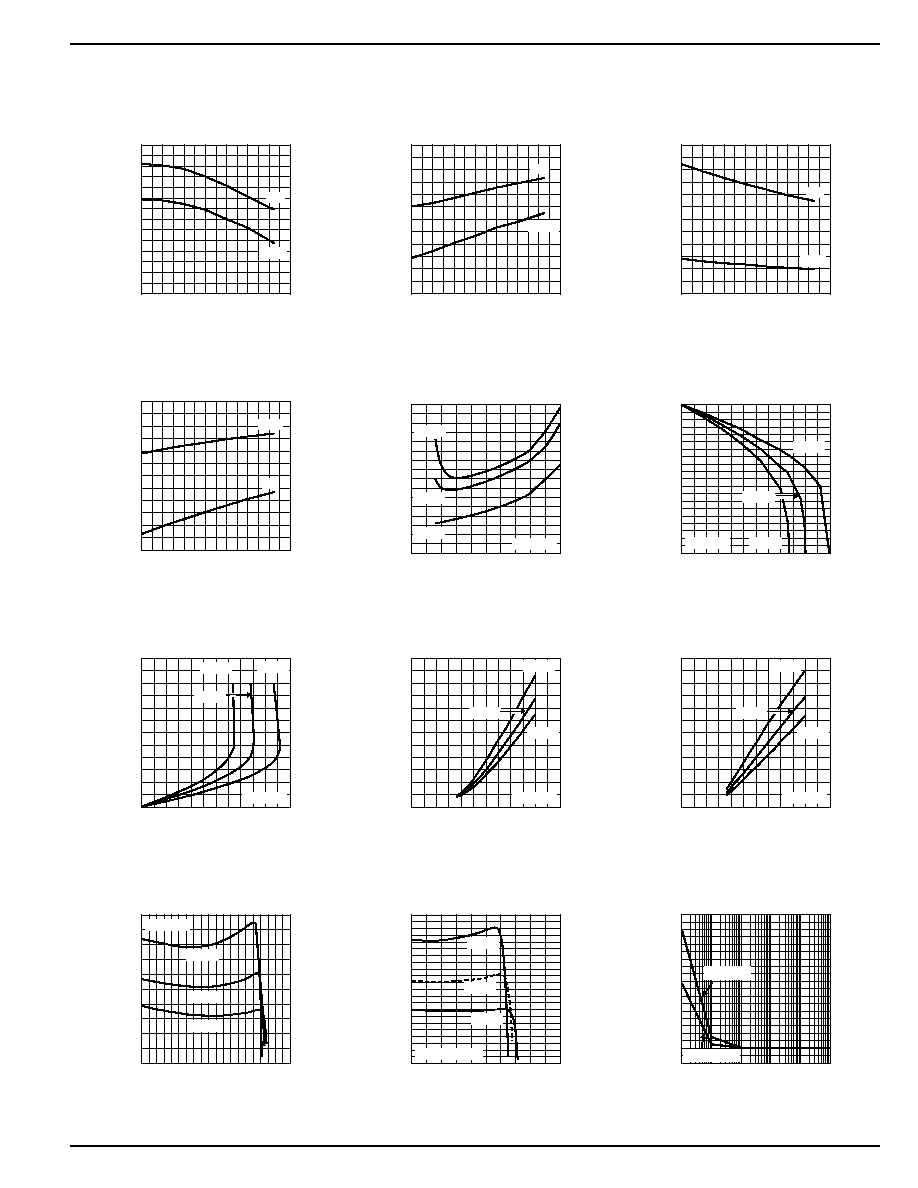
25
27
29
31
33
35
37
39
-40 -20
0
20
40
60
80 100
SUPPLY CURRENT (
µ
A)
TEMPERATURE (
∞
C)
Supply Current
vs. Temperature
5V
2.7V
-60
-50
-40
-30
-20
-10
0
-40 -20
0
20
40
60
80 100
SHORT CIRCUIT CURRENT (mA)
TEMPERATURE (
∞
C)
Short Circuit Current (sink)
vs. Temperature
5V
2.7V
0
5
10
15
20
25
30
-40 -20
0
20
40
60
80 100
SHORT CIRCUIT CURRENT (mA)
TEMPERATURE (
∞
C)
Short Circuit Current (source)
vs. Temperature
5V
2.7V
-6
-5.5
-5
-4.5
-4
-3.5
-3
-40 -20
0
20
40
60
80 100
OFFSET VOLTAGE (mV)
TEMPERATURE (
∞
C)
Offset Voltage
vs. Temperature
5V
2.7V
Typical Characteristics
25
27
29
31
33
35
37
39
41
0.5
1
1.5
2
2.5
3
SUPPLY CURRENT (
µ
A)
SUPPLY VOLTAGE (
±
V)
Supply Current vs.
Supply Voltage
-40
∞
C
+85
∞
C
+25
∞
C
V+ = 5V
0
0.5
1
1.5
2
2.5
3
3.5
4
4.5
5
0
5
10
15
20
25
30
OUTPUT VOLTAGE (V)
OUTPUT CURRENT (mA)
Output Voltage vs.
Output Current (Sourcing)
-40
∞
C
+85
∞
C
+25
∞
C
V+ = 5V
0
1
2
3
4
5
6
0
10
20
30
40
50
60
OUTPUT VOLTAGE (V)
OUTPUT CURRENT (mA)
Output Voltage vs.
Output Current (Sinking)
-40
∞
C
+85
∞
C
+25
∞
C
V+ = 5V
0
5
10
15
20
25
30
0
0.5
1
1.5
2
2.5
3
OUTPUT CURRENT (mA)
SUPPLY VOLTAGE (
±
V)
Short Circuit Current vs.
Supply Voltage (Sourcing)
-40
∞
C
+85
∞
C
+25
∞
C
V+ = 5V
0
10
20
30
40
50
60
0
0.5
1
1.5
2
2.5
3
OUTPUT CURRENT (mA)
SUPPLY VOLTAGE (
±
V)
Short Circuit Current vs.
Supply Voltage (Sinking)
-40
∞
C
+85
∞
C
+25
∞
C
V+ = 5V
0
0.5
1
1.5
2
2.5
0 0.5 1 1.5 2 2.5 3 3.5 4 4.5 5
OFFSET VOLTAGE (mV)
COMMON-MODE VOLTAGE (V)
Offset Voltage vs.
Common-Mode Voltage
-40
∞
C
+85
∞
C
+25
∞
C
V+ = 5V
0
0.2
0.4
0.6
0.8
1.0
1.2
1.4
1.6
1.8
2.0
2.2
0
0.54
1.08
1.62
2.16
2.7
OFFSET VOLTAGE (mV)
COMMON-MODE VOLTAGE (V)
Offset Voltage vs.
Common-Mode Voltage
-40
∞
C
+85
∞
C
+25
∞
C
Supply = 2.7V
-0.5
0
0.5
1
1.5
2
2.5
3
3.5
4
4.5
0.1
1
10
100
1000 10000
OUTPUT VOLTAGE (V)
RESISTIVE LOAD (k
)
Output Voltage Swing vs.
Resistive Load (Sinking)
V
CC
= 5V
V
CC
= 2.7V