 | –≠–ª–µ–∫—Ç—Ä–æ–Ω–Ω—ã–π –∫–æ–º–ø–æ–Ω–µ–Ω—Ç: MICRF008 | –°–∫–∞—á–∞—Ç—å:  PDF PDF  ZIP ZIP |

July 2003
1
MICRF008
MICRF008
Micrel
MICRF008
QwikRadioTM Sweep-Mode Receiver
General Description
The MICRF008 QwikRadioTM UHF receiver is a single-chip
OOK (on-off keyed) receiver IC designed for remote wireless
applications. This device is a true single-chip, "antenna-in,
data-out" device, and it is easy to implement. MICRF008
receiver requires very few peripheral passive components.
All tunings, RF and IF, are accomplished within the IC. Ease
of use and minimal parts count translate to cost savings and
shorter time to market. MICRF008 receiver offers a robust
and low-cost solution for high volume wireless applications.
The MICRF008 sweeps the internal local oscillator at rates
greater than the baseband data rate. This effectively broad-
ens the RF bandwidth of the receiver to a value equivalent to
conventional superregenerative receivers. This allows the
MICRF008 to operate with less expensive LC transmitters
without additional components or tuning, even though the
receiver topology is still superheterodyne. In this mode the
reference crystal can be replaced with a less expensive
±
0.5% ceramic resonator.
Since all post-detection (demodulator) data filtering is pro-
vided on the MICRF008, no external IF filters are required.
One of the two internal filter bandwidths must be externally
selected based on data rate and code modulation format.
Typical Application
SEL0
VSS
REFOSC
ANT
CAGC
VDD
CTH
DO
C3
0.1
µ
F
C1
1.8pF
L1
33nH
C4
2.2
µ
F
U1
MICRF008BM
+5V
C2
4.7
µ
F
Y1
3.36MHz
ANT1
1/8 Monopole
80mm
1
2
3
4
8
7
6
5
433.92MHz Receiver
Features
∑ Complete UHF receiver on a monolithic chip
∑ 300MHz to 440MHz frequency range
∑ Up to 4.8kbps data rate.
∑ Automatic tuning, no manual adjustment
∑ Very low RF antenna reradiation
∑ CMOS logic interface for standard ICs
∑ Low external part count
∑ Replaces superregenerative receivers design
∑ Manufacturability and same performance over the years
∑ Very small PCB area required
Applications
∑ Garage door and gate openers
∑ Security systems
∑ Remote appliances control
∑ Toys
∑ Fan and light control
Ordering Information
Part Number
Junction Temp. Range
Package
MICRF008BM
≠40
∞
C to +85
∞
C
8-Pin SOIC
Micrel, Inc. ∑ 1849 Fortune Drive ∑ San Jose, CA 95131 ∑ USA ∑ tel + 1 (408) 944-0800 ∑ fax + 1 (408) 944-0970 ∑ http://www.micrel.com
QwikRadioTM is a trademark of Micrel.

MICRF008
Micrel
MICRF008
2
July 2003
Pin Description
Pin Number
Pin Name
Pin Function
1
SEL0
Bandwidth Selection Bit 0 (Input): Sets the desired demodulator filter
bandwidth. See Table 1. Internally pulled-up to V
DD
.
2
ANT
Antenna (Input): High-impedance, internally AC-coupled receiver input.
Connect this pin to the matching network. See
"Applications Information"
for
optional band-pass filter information.
3
VDD
Positive Supply Input: Connect a low ESL, low ESR decoupling capacitor
from this pin to V
SS
, as short as possible.
4
CTH
[Data Slicing] Threshold Capacitor (External Component): Capacitor
extracts the DC average value from the demodulated waveform which
becomes the reference for the internal data slicing comparator. See
"Appli-
cations Information"
for selection.
5
DO
Digital Output (Output): CMOS-level compatible data output signal.
6
VSS
Negative Supply Input: Connect this pin to the RF ground.
7
CAGC
AGC Capacitor (External Component): Integrating capacitor for on-chip
AGC (automatic gain control). The decay/attack time-constant (
) ratio is
nominally 10:1. See
"Applications Information"
for capacitor selection.
8
REFOSC
Reference Oscillator (External Component or Input): Timing reference for
on-chip tuning and alignment. Connect either a ceramic resonator or a
crystal between this pin and V
SS
, or drive the input with an AC-coupled
0.5V
PP
input clock.
Pin Configuration
1
SEL0
ANT
VDD
CTH
8
REFOSC
CAGC
VSS
DO
7
6
5
2
3
4
8-Pin SOP (M)

July 2003
3
MICRF008
MICRF008
Micrel
Electrical Characteristics
(Note 4)
+4.75V
V
DD
5.5V, V
SS
= 0V; C
AGC
= 4.7
µ
F, C
TH
= 2.2
µ
F no preamble for data; f
REFOSC
= 3.36MHz; T
A
= 25
∞
C, bold values
indicate ≠40
∞
C
T
A
+85
∞
C; current flow into device pins is positive; unless noted.
Symbol
Parameter
Condition
Min
Typ
Max
Units
I
OP
Operating Current
continuous 315MHz operation
7
9
mA
continuous 433.92MHz operation
13
16
mA
reference oscillator powered down
2
2.5
mA
RF Section, IF Section
Receiver Sensitivity
315MHz, SEL0 = 0V; Notes 5, 6
≠90
≠95
dBm
433.92MHz, SEL0 = 0V; Notes 5, 6
≠90
≠95
dBm
f
IF
IF Center Frequency
Note 7
2.0
MHz
f
BW
IF Bandwidth
315MHz; Note 6, 7
0.8
MHz
433.92MHz; Note 6, 7
1.1
MHz
Maximum Receiver Input
R
SC
= 50
≠20
dBm
Spurious Reverse Isolation
ANT pin, R
SC
= 50
, Note 8
30
µ
Vrms
AGC Attack to Decay Ratio
t
ATTACK
˜
t
DECAY
0.1
Reference Oscillator
Reference Oscillator
7
µ
A
Source Current
Z
REFOSC
Reference Oscillator
Note 9
200
k
Input Impedance
Demodulator
Z
CTH
C
TH
Source Impedance
V
SEL0
= V
DD
, See Table 1, Note 10
220
k
Z
CTH
Maximum C
TH
Source Impedance
±
15
%
Variation
Digital/Control Section
Z
IN(pu)
Input Pull-Up Impedance
SEL0
1.0
M
I
OUT
Output Current
DO pin, push-pull
10
µ
A
V
OUT(high)
Output High Voltage
DO pin, I
OUT
= 1
µ
A
0.8V
DD
V
V
OUT(low)
Output Low Voltage
DO pin, I
OUT
= 1
µ
A
0.2V
DD
V
t
R
, t
F
Output Rise and Fall Times
DO pin, C
LOAD
= 15pF
10
µ
s
Note 1.
Exceeding the absolute maximum rating may damage the device.
Note 2.
The device is not guaranteed to function outside its operating rating.
Note 3.
Devices are ESD sensitive. Use appropriate ESD precautions. Meets Class 1 ESD test requirements, (human body model, HBM), in accor-
dance with MIL-STD-883C, method 3015. Do not operate or store near strong electrostatic fields.
Note 4.
Specification for packaged product only.
Note 5.
Sensitivity is defined as the average signal level measured at the input necessary to achieve 10
≠2
BER (bit error rate). The input signal is
defined as a return-to-zero (RZ) waveform with 50% average duty cycle at a data rate of 1kbps (Manchester encoded). The RF input is
assumed to be matched into 50
.
Absolute Maximum Ratings
(Note 1)
Supply Voltage (V
DDRF
, V
DDBB
) .................................... +7V
Reference Oscillator Input Voltage (V
REFOSC
) .......... V
DDBB
Input/Output Voltage (V
I/O
) ................. V
SS
≠0.3 to V
DD
+0.3
Junction Temperature (T
J
) ...................................... +150
∞
C
Storage Temperature Range (T
S
) ............ ≠65
∞
C to +150
∞
C
Lead Temperature (soldering, 10 sec.) ................... +260
∞
C
ESD Rating, Note 3
Operating Ratings
(Note 2)
Supply Voltage (V
DD
) ................................ +4.75V to +5.5V
Ambient Temperature (T
A
) ......................... ≠40
∞
C to +85
∞
C
RF Operating Range ........................... 300MHz to 440MHz
Data Duty Cycle ............................................... 20% to 80%
Reference Oscillator Input Range ............ 0.2V
PP
to 1.5V
PP
Demod Bandwidth .......................................... 0.1 to 4.8kHz

MICRF008
Micrel
MICRF008
4
July 2003
Note 6.
Sensitivity, a commonly specified receiver parameter, provides an indication of the receiver's input referred noise, generally input thermal
noise. However, it is possible for a more sensitive receiver to exhibit range performance no better than that of a less sensitive receiver if the
background noise is appreciably higher than the thermal noise. Background noise refers to other interfering signals, such as FM radio
stations, pagers, etc.
A better indicator of achievable receiver range performance is usually given by its selectivity, often stated as intermediate frequency (IF) or
radio frequency (RF) bandwidth, depending on receiver topology. Selectivity is a measure of the rejection by the receiver of ambient noise.
More selective receivers will almost invariably provide better range. Only when the receiver selectivity is so high that most of the noise on the
receiver input is actually thermal will the receiver demonstrate sensitivity-limited performance.
Note 7.
Parameter scales linearly proportional with reference oscillator frequency f
T
. For any reference oscillator frequency other than 3.36 MHz,
compute new parameter value as the ratio:
f
MHz
3 36MHz
parameter value at 3.36MHz
REFOSC
.
◊
(
)
Note 8.
Spurious reverse isolation represents the spurious components which appear on the RF input pin (ANT) measured into 50
with an input RF
matching network.
Note 9.
Series resistance of the resonator (ceramic or crystal) should be minimized to the extent possible, to ensure oscillation. In case where the
resonator series resistance is too great, the oscillator may oscillate at a diminished peak-to-peak level, or may fail to oscillate entirely. Micrel
recommends that series resistances for ceramic resonators and crystals not exceed 50
and 100
respectively.
Note 10. Parameter scales inversely proportional with reference oscillator frequency f
T
. For any reference oscillator frequency other than 3.36 MHz,
compute new parameter value as the ratio:
3 36MHz
F
MHz
parameter value at 3.36MHz
REFOSC
.
◊
(
)
C
TH
source impedance in Table 1 is represented by (sym-
bolic) resistor RSC in the MICRF008 Simplified Block Dia-
gram. The Programmable LPF (Low Pass Filter) is also
illustrated in the MICRF008 Simplified Block Diagram.
SEL0
Programmable LPF
C
TH
Source
Bandwidth (Hz)
Impedance (
)
0
2400
440k
1
4800
220k
Table 1. Nominal Characteristics
Programmable LPF Bandwidth and C
TH
Source
Impedance
Typical Characteristics
4
6
8
10
12
14
16
18
250
300
350
400
450
500
CURRENT (mA)
FREQUENCY (MHz)
Supply Current
vs. Frequency
T
A
= 25
∞
C
V
DD
= 5V
0
2
4
6
8
10
12
14
16
18
-40 -20
0
20
40
60
80 100
CURRENT (mA)
TEMPERATURE (
∞
C)
Supply Current
vs. Temperature
f = 315MHz
V
DD
= 5V
July 2003
5
MICRF008
MICRF008
Micrel
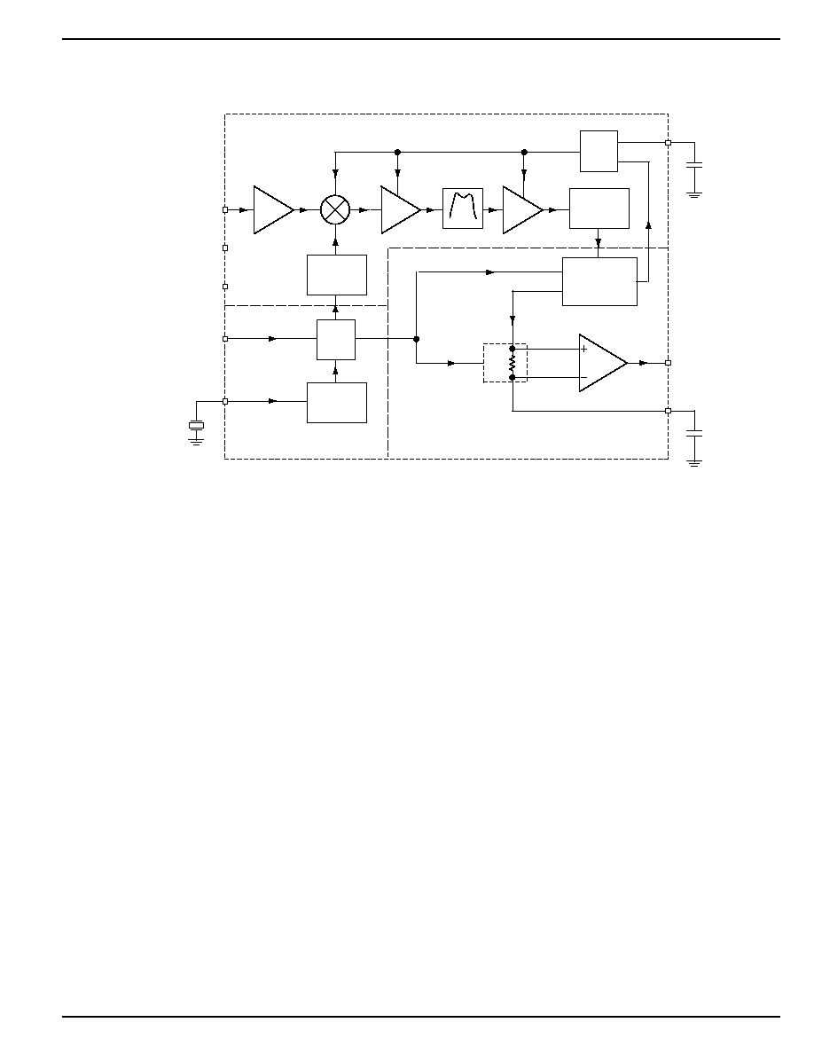
Functional Description
The entire block diagram illustrates the basic structure of the
MICRF008BM. It is made of three sub-blocks, which are the
UHF Downconverter, the OOK Demodulator, and the Refer-
ence and Control. Also shown in the figure are two capacitors
(C
TH
, and C
AGC
) and the reference frequency device, usually
a ceramic resonator. With the exception of a supply decoupling
capacitor and the matching network on the antenna pin, these
are all the external components needed with the MICRF008BM
to make a complete UHF receiver. There is one control input,
the SEL0 pin. The purpose is to set the demodulator filter
bandwidth of either 2.4kHz or 4.8kHz, and is set high or low
according to the minimum pulse width in the demodulated
signal. The input is CMOS compatible, and is pulled-up
internally in the IC.
Receiver Operation
The MICRF008BM is a superheterodyne receiver working in
sweep mode. It is capable of data rates up to
9.6kbaud NRZ or 4.8kbaud Manchester encoded. The
MICRF008BM RF center frequency is controlled by a com-
Functional Diagram
Comparator
ANT
VCC
VSS
SEL0
REFOSC
Ceramic
Resonator
CAGC
RF
Amp
t
RF
t
IF
t
LO
R
BC
mboer
1MHz
Programmable
Low-Pass
Filter
Peak
Detector
Reference
Oscillator
Synthesizer
Control
Logic
IF
Amp
IF
Amp
CTH
DO
OOK Demodulator
UHF Downconverter
Switched-Cap
Resistor
Reference and Control
AGC
Control
pletely integrated PLL/VCO frequency synthesizer with
frequency set by a ceramic resonator. The actual swept
bandwidth is approximately 3% of the RF carrier frequency.
It makes an ideal part to work with LC-based transmitters or
other types of transmitters that are not precise in nature and
vary their frequency with time. In sweep mode the LO
frequency (local oscillator) is varied in a rate much higher
than the data signal, which results in down-conversion of
approximately 3% of the carrier frequency present at the
antenna pin. The low level RF signal is amplified by the RF
amp section and downconverted by the mixer to the IF
frequency which is amplified and filtered internally in the
device and further amplified for the peak detector. The peak
detector will detect the IF and further filtering is accomplished
in the programmable low-pass filter. The detected/filtered
signal is compared with the DC value of the demodulated
signal in the data-slicer and a digital output is provided from
the DO pin.