
1
Pin
Function
CLK, /CLK
Differential Clock Inputs
D[0:1], /D[0:1]
Differential Data Inputs
Q[0:1], /Q[0:1]
Differential Data Outputs
R
0
, R
1
Reset Inputs
S
0
, S
1
Set Inputs
V
BB
V
BB
Reference Output
V
CC
V
CC
V
EE
V
EE
DESCRIPTION
FEATURES
s
3.3V and 5V power supply option
s
Differential D, CLK and Q
s
Extended V
EE
range of ≠3.0V to ≠5.5V
s
V
BB
output for single-ended use
s
1100MHz min. toggle frequency
s
Asynchronous Reset and Set
s
Fully compatible with Motorola MC100LVEL29 and
MC100EL29
s
Available in 20-pin SOIC package
5V/3.3V DUAL DIFFERENTIAL
DATA AND CLOCK
D FLIP-FLOP w/SET AND RESET
ClockWorksTM
SY100EL29V
Rev.: B
Amendment: /0
Issue Date:
February 2000
PIN NAMES
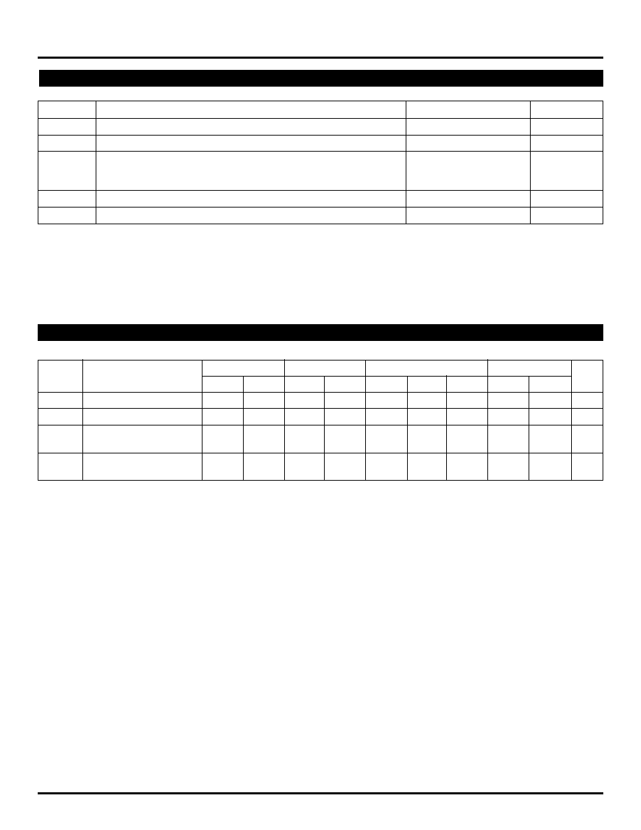
PIN CONFIGURATION/BLOCK DIAGRAM
1
D0
D0 CLK0 CLK0 VBB D1
D1 CLK1 CLK1 R1
20
R0 VCC Q0
Q0
S0
S1 VCC Q1
Q1
V
EE
2
19
3
18
4
17
5
16
6
15
7
14
8
13
9
12
10
11
Q
Q
R
S
D
CLK
Q
Q
R
D
S
CLK
SOIC
TOP VIEW
R
S
D
CLK
Q
/Q
L
L
L
Z
L
H
L
L
H
Z
H
L
H
L
X
X
L
H
L
H
X
X
H
L
H
H
X
X
Undef
Undef
TRUTH TABLE
NOTE:
Z = LOW-to-HIGH Transition
The SY100EL29V is a dual differential register with
differential data (inputs and outputs) and clock. The
registers are triggered by a positive transition of the
positive clock (CLK) input. A HIGH on the Reset (R
x
)
asynchronously resets the appropriate register so that
the Q outputs go LOW. A HIGH on the Set (S
x
)
asynchronously resets the appropriate register so that
the Q outputs go HIGH. The Set and Reset inputs cannot
both be HIGH simultaneously.
The differential input structures are clamped so that
the inputs of unused registers can be left open without
upsetting the bias network of the devices. The clamping
action will assert the /D and the /CLK sides of the inputs.
The noninverting input will pull down to V
EE
and the
inverting input will be biased around V
CC
/2. Because of
the edge-triggered flip-flop nature of the devices,
simultaneously opening both the clock and data inputs
will result in an output which reaches an unidentified but
valid state.
The fully differential design of the devices makes them
ideal for very high frequency applications where a
registered data path is necessary.
2
ClockWorksTM
SY100EL29V
Micrel
Symbol
Rating
Value
Unit
V
EE
Power Supply (V
CC
= 0V)
≠8.0 to 0
VDC
V
I
(3)
Input Voltage (V
CC
= 0V)
0 to ≠6.0
VDC
I
OUT
Output Current
≠Continuous
50
mA
≠Surge
100
T
A
Operating Temperature Range
≠40 to +85
∞
C
V
EE
Operating Range
(1),(2)
≠5.7 to ≠3.0
V
NOTES:
1. Absolute maximum rating, beyond which, device life may be impaired, unless otherwise specified on an individual data sheet.
2. Parametric values specified at:
100EL29V Series:
≠3.0V to ≠5.5V.
3. In PECL mode operation, V
I
(Max) = V
CC
.
ABSOLUTE MAXIMUM RATINGS
(1)
T
A
= ≠40
∞
C
T
A
= 0
∞
C
T
A
= +25
∞
C
T
A
= +85
∞
C
Symbol
Parameter
Min.
Max.
Min.
Max.
Min.
Typ.
Max.
Min.
Max.
Unit
I
EE
Power Supply Current
--
50
--
50
--
30
50
--
50
mA
I
IH
Input HIGH Current
--
150
--
150
--
--
150
--
150
µ
A
I
IL
Input LOW Current
0.5
--
0.5
--
0.5
--
--
0.5
--
µ
A
/CLK, /Dn
≠300
--
≠300
--
≠300
--
--
≠300
--
V
BB
Output Reference
≠1.38
≠1.26
≠1.38
≠1.26
≠1.38
--
≠1.26
≠1.38
≠1.26
V
Voltage
DC ELECTRICAL CHARACTERISTICS
V
EE
= ≠3.0V to +5.5V; V
CC
= GND

3
ClockWorksTM
SY100EL29V
Micrel
T
A
= ≠40
∞
C
T
A
= 0
∞
C
T
A
= +25
∞
C
T
A
= +85
∞
C
Symbol
Parameter
Min.
Max.
Min.
Max.
Min.
Typ.
Max.
Min.
Max.
Unit
f
MAX
Max. Toggle Frequency
1.1
--
1.1
--
1.1
--
--
1.1
--
GHz
t
PLH
Propagation Delay
CLK
480
680
490
690
500
--
700
520
720
ps
t
PHL
to Output
S, R
450
670
450
670
450
--
670
450
670
t
S
Set-Up Time, D
200
--
200
--
200
--
--
200
--
ps
t
H
Hold Time, D
150
--
150
--
150
--
--
150
--
ps
t
RR
Reset Recovery Time
300
--
300
--
300
--
--
300
--
ps
t
PW
Minimum Pulse Width
400
--
400
--
400
--
--
400
--
ps
CLK, Set, Reset
V
CMR
Common Mode Range
(1)
V
<500mV
≠2.0
≠0.4
≠2.1
≠0.4
≠2.1
--
≠0.4
≠2.1
≠0.4
500mV
≠1.8
≠0.4
≠1.9
≠0.4
≠1.9
--
≠0.4
≠1.9
≠0.4
V
PP (AC)
Minimum Input Swing
(2)
150
--
150
--
150
--
--
150
--
mV
t
r
Output Rise/Fall Time Q
280
550
280
550
280
330
550
280
550
ps
t
f
(20≠80%)
AC ELECTRICAL CHARACTERISTICS
V
EE
= ≠3.0V to +5.5V; V
CC
= GND
NOTES:
1. V
CMR
is referenced to the most positive side of the differential input signal. Normal operation is obtained when the input signals are within the V
CMR
range
and the input swing is greater than V
PP
(Min.) and <1V. The lower end of the V
CMR
range varies 1:1 with V
EE
. The numbers in the spec table assume a nominal
V
EE
= ≠3.3V. Note for PECL operation, the V
CMR
(Min) will be fixed at 3.3V ≠ |V
CMR
(Min)|.
2. Minimum input swing for which AC parameters are guaranteed.
PRODUCT ORDERING CODE
Ordering
Package
Operating
Code
Type
Range
SY100EL29VZC
Z20-1
Commercial
SY100EL29VZCTR
Z20-1
Commercial
4
ClockWorksTM
SY100EL29V
Micrel
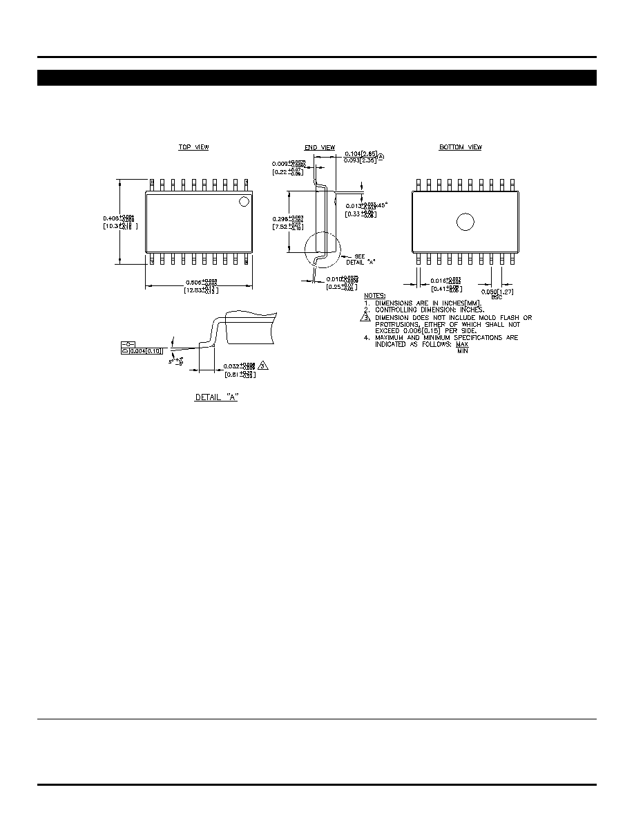
20 LEAD SOIC .300" WIDE (Z20-1)
Rev. 03
MICREL-SYNERGY
3250 SCOTT BOULEVARD
SANTA CLARA
CA 95054
USA
TEL
+ 1 (408) 980-9191
FAX
+ 1 (408) 914-7878
WEB
http://www.micrel.com
This information is believed to be accurate and reliable, however no responsibility is assumed by Micrel for its use nor for any infringement of patents or
other rights of third parties resulting from its use. No license is granted by implication or otherwise under any patent or patent right of Micrel Inc.
© 2000 Micrel Incorporated