 | –≠–ª–µ–∫—Ç—Ä–æ–Ω–Ω—ã–π –∫–æ–º–ø–æ–Ω–µ–Ω—Ç: SY100S324 | –°–∫–∞—á–∞—Ç—å:  PDF PDF  ZIP ZIP |

DESCRIPTION
FEATURES
s
Max. propagation delay of 1.4ns
s
I
EE
min. of ≠70mA
s
Industry standard 100K ECL levels
s
Extended supply voltage option:
V
EE
= ≠4.2V to ≠5.5V
s
Differential outputs
s
Voltage and temperature compensation for improved
noise immunity
s
Internal 75K
input pull-down resistors
s
Twice as fast as Fairchild's 324
s
Function and pinout compatible with Fairchild F100K
s
Available in 24-pin CERPACK and 28-pin PLCC
packages
The SY100S324 is a hex translator designed to convert
TTL logic levels to 100K ECL levels. The inputs are TTL
compatible with differential outputs that can either be
used as an inverting/non-inverting translator or as
differential line drivers. A common Enable (E), when LOW,
holds all inverting outputs HIGH and holds all non-
inverting outputs LOW.
When used in the differential mode, due to its high
common mode rejection, it overcomes voltage gradients
between the TTL and ECL ground systems. The V
EE
and
V
TTL
power may be applied in either order.
LOW POWER HEX
TTL-to-ECL
TRANSLATOR
PIN CONFIGURATIONS
SY100S324
Rev.: F
Amendment: /0
Issue Date:
July, 1999
Pin
Function
D
0
≠D
5
Data Inputs
E
Enable Inputs
Q
0
≠Q
5
Data Outputs
Q
0
≠Q
5
Complementary Data Outputs
V
EES
V
EE
Substrate
V
TTL
TTL V
CC
Power Supply
V
CCA
V
CCO
for ECL Outputs
PIN NAMES
18
17
16
15
14
13
12
5
6
7
8
9
10
11
2
3
4
1
Top View
Flatpack
F24-1
24
23
22
21
20
19
E
V
EE
D
3
D
0
D
4
V
TT
L
D
2
Q
0
Q
1
D
1
Q
0
Q
1
V
CC
V
CCA
Q
3
Q
2
V
CCA
Q
2
D
5
Q
5
Q
4
Q
5
Q
4
Q
3
18
17
16
15
14
13
12
D
0
V
TTL
E
V
EES
V
EE
D
3
D
4
5
6
7
8
9
10 11
26
27
28
1
2
3
4
Top View
PLCC
J28-1
25 24 23 22 21 20 19
Q
2
V
CC
V
CC
V
CCA
V
CCA
Q
3
Q
2
Q
4
V
EES
Q
5
D
5
Q
3
Q
4
Q
5
V
EES
Q
0
D
2
Q
1
D
1
Q
1
Q
0
BLOCK DIAGRAM
D
0
Q
0
Q
0
E
D
1
Q
1
Q
1
D
2
Q
2
Q
2
D
3
Q
3
Q
3
D
4
Q
4
Q
4
D
5
Q
5
Q
5
1

2
SY100S324
Micrel
AC ELECTRICAL CHARACTERISTICS
PLCC /FLATPACK
V
EE
= ≠4.2V to ≠5.5V unless otherwise specified, V
CC
= V
CCA
= GND, V
TTL
= +4.5V to +5.5V
DC ELECTRICAL CHARACTERISTICS
V
EE
= ≠4.2V to ≠5.5V unless otherwise specified, V
CC
= V
CCA
= GND, V
TTL
= +4.5V to +5.5V
Symbol
Parameter
Min.
Sim.
Max.
Unit
Condition
V
OH
Output HIGH Voltage
≠1025
≠986
≠880
mV
V
IN
= V
IH
(Max.)
Loading with 50
V
OL
Output LOW Voltage
≠1810
≠1674
≠1620
mV
V
IN
= V
IL
(Min.)
V
OHC
Output HIGH Voltage
≠1035
--
--
mV
V
IN
= V
IH
(Min.)
Loading with 50
to ≠2V
V
OLC
Output LOW Voltage
--
--
≠1610
mV
V
IN
= V
IL
(Max.)
V
IH
Input HIGH Voltage
2.0
--
5.0
V
Guaranteed HIGH Signal for All Inputs
V
IL
Input LOW Voltage
0
--
0.8
V
Guaranteed LOW Signal for All Inputs
V
CD
Input Clamp Diode Voltage
--
--
≠1.5
V
I
IN
= ≠10mA
I
IH
Input HIGH Current
Data
--
--
20
µ
A
V
IN
= +2.4V
Enable
--
--
120
All Other Inputs V
IN
= GND
I
IH
Input HIGH Current
--
--
1.0
mA
V
IN
= +5.5V, V
TTL
= Max.,
Breakdown Test, All Inputs
All Other Inputs V
IN
= GND
I
IL
Input LOW Current
Data
≠1.2
--
--
mA
V
IN
= +0.4V
Enable
≠6.7
--
--
All Other Inputs V
IN
= V
IH
I
EE
V
EE
Power Supply Current
≠70
≠45
≠28
mA
All Inputs V
IN
= +4.0V
I
TTL
V
TTL
Power Supply Current
--
25
35
mA
All Inputs V
IN
= GND
Symbol
Parameter
Min.
Typ.
Max.
Unit
Condition
t
PLH
Propagation Delay
400
850
1400
ps
See Switching Wave Form Figures
t
PHL
Data and Enable to Output
t
TLH
Transition Time
350
--
1700
ps
t
THL
20% to 80%, 80% to 20%
3
SY100S324
Micrel
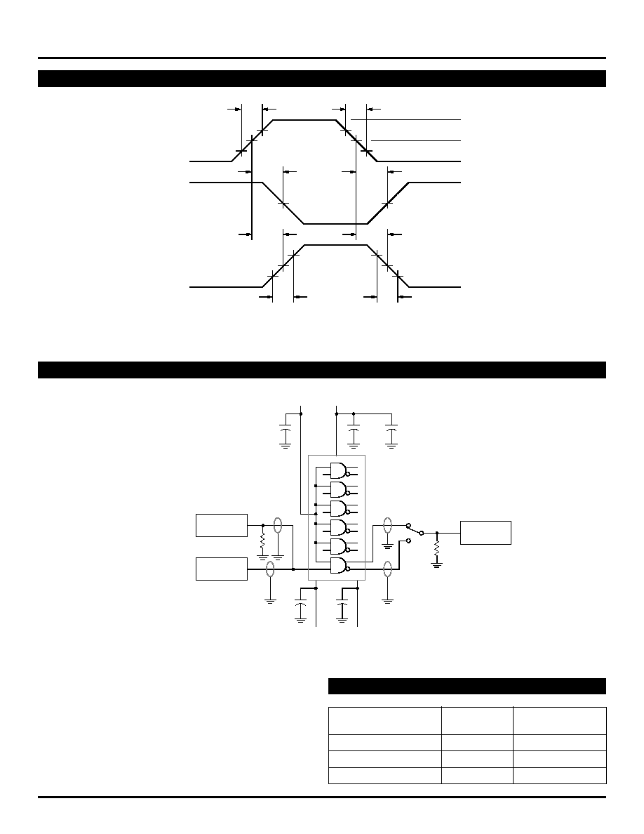
SWITCHING WAVEFORM
Figure 1. Propagation Delay and Transition Times
TEST CIRCUIT
Figure 2. AC Test Circuit
NOTES:
V
CC
, V
CCA
= +2V, V
EE
= ≠2.5V, V
TTL
= +7.0V, V
IH
= +6.0V
L1, L2 and L3 = equal length 50
impedance lines
R
T
= 50
terminator internal to scope
Decoupling 0.1
µ
F from GND to V
CC
, V
EE
and V
TTL
All unused outputs are loaded with 50
to GND
C
L
= Fixture and stray capacitance
3pF
PULSE
GENERATOR
SCOPE
CHAN A
V
IH
V
TTL
0.1
µ
F
L2
L3
R
T
V
EE
V
CC
2.5
µ
F
L1
R
T
0.1
µ
F
0.1
µ
F
0.1
µ
F
SCOPE
CHAN B
PRODUCT ORDERING CODE
Ordering
Package
Operating
Code
Type
Range
SY100S324FC
F24-1
Commercial
SY100S324JC
J28-1
Commercial
SY100S324JCTR
J28-1
Commercial
NOTE:
V
EE
= ≠4.2V to ≠5.5V unless otherwise specified, V
CC
= V
CCA
= GND, V
TTL
= +4.5V to +5.5V
COMPLEMENT
t
PLH
t
THL
INPUT
TRUE
t
PHL
t
PLH
50%
2.5
±
0.3 ns
2.5
±
0.3 ns
+3.0V
20%
80%
50%
20%
80%
50%
+1.5V
0V
t
TLH
t
PHL
4
SY100S324
Micrel
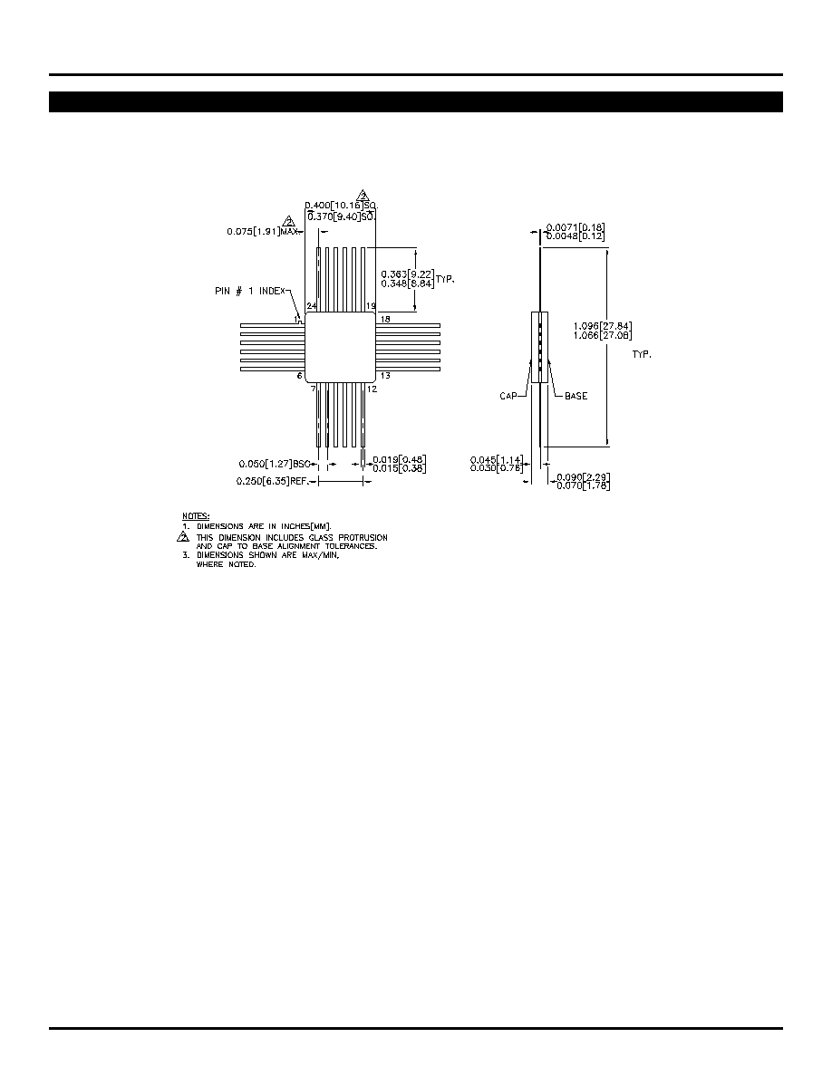
24 LEAD CERPACK (F24-1)
Rev. 03
5
SY100S324
Micrel
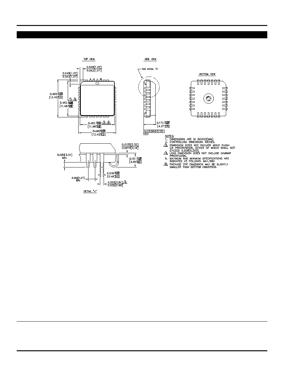
28 LEAD PLCC (J28-1)
Rev. 03
MICREL-SYNERGY
3250 SCOTT BOULEVARD
SANTA CLARA
CA 95054
USA
TEL
+ 1 (408) 980-9191
FAX
+ 1 (408) 914-7878
WEB
http://www.micrel.com
This information is believed to be accurate and reliable, however no responsibility is assumed by Micrel for its use nor for any infringement of patents or
other rights of third parties resulting from its use. No license is granted by implication or otherwise under any patent or patent right of Micrel Inc.
© 2000 Micrel Incorporated