
1
January 1997
ML6680
Token Ring Copper-to-Fiber Converter
GENERAL DESCRIPTION
The ML6680 is a single-chip conversion between Token
Ring ISO/IEC8802-5 copper-based media and Token Ring
ISO/IEC8802-5 fiber-based media. The ML6680 fiber-optic
interface contains a data quantizer, circuitry for fiber optic
key signal generation and recognition, pin-selectable
signal switching, and current driven transmitter outputs.
The ML6680 copper interface consists of a twisted pair
line equalizer, receive squelch circuit, pin selectable
phantom wire fault detection and signal switching, and a
transmit driver. This section supports the ISO/IEC8802-5
standard requirements. The ML6680 provides an optional
PECL compatible interface.
The ML6680 may be configured to one of four modes:
1. Standard Media Converter
2. Concentrator Media Converter
3. Lobe or Ring Out Port Media Converter
4. Ring In Port Media Converter
FEATURES
s
Single-chip copper-to-fiber converter for Token Ring
s
16Mbps and 4Mbps data rates with the same
external components
s
Four modes of operation covering a wide variety
of applications
s
Full duplex operation
s
Highly stable data quantizer with 55dB input
dynamic range
s
Current driven fiber optic LED driver for accurate
launch power
s
Current driven output for low RFI noise and low jitter
s
Capable of driving 100
UTP or 150
STP
s
Pin selectable phantom wire fault detection and
signal switching
TWISTED PAIR
EQUALIZER
TWISTED PAIR
RECEIVE SQUELCH
TWISTED PAIR
DRIVER
PHANTOM
DRIVER
LED
DRIVER
FIBER OPTIC
RECEIVE SQUELCH
FIBER OPTIC
QUANTIZER
BIAS
CONTROL
LOGIC
CRYSTAL
OSCILLATOR
SIGNAL
MUX
TPINP
TPINN
OPVCC
OPOUT
TPOUTP
TPINOK
RTSETTP
TPOUTN
OPINP
OPINOK
OPINN
PHTM1
PHTM2
XTAL1
VDC
XTAL2
KEYGEN
INSERTED
EQA
EQB
RTSETOP
BLOCK DIAGRAM
ML6680
2
PIN CONFIGURATION
ML6680
28-Pin PLCC (Q28)
OPINN
QGND
VDC
KEYGEN
GND1
OPGND
OPOUT
TPINP
TPINN
PHTM1
PHTM2
GND2
TPOUTP
TPOUTN
12
13 14
15
16
EQB
EQA
VCC2
XTAL1
XTAL2
QVCC
OPINP
TPINOK
RTSETTP
VCC1
INSERTED
RTSETOP
OPINOK
OPVCC
17
18
5
6
7
8
9
10
11
4
3
2
1
28
25
24
23
22
21
20
19
27
26
TOP VIEW

ML6680
3
PIN DESCRIPTION
PIN# NAME
FUNCTION
1, 28 XTAL1,
Crystal inputs. A 32.768kHz watch
XTAL2
crystal connected between these pins
provides timing for the fiber optic
insertion key signal. An external clock
can be used to drive XTAL1 while
grounding XTAL2. The frequency of
the external clock should be between
32.7kHz and 34.5kHz.
2
V
CC2
Positive 5V power supply.
3, 4 EQA, EQB Equalizer network pins. An external
combination of two resistors and a
capacitor connected at EQA and EQB
sets up the on-chip twisted pair
receive equalizer.
5, 6 TPINP/N
Receive twisted pair inputs. This
differential input pair receives
differential Manchester signals from
the coupling transformer (or PECL
compatible levels).
7, 8 PHTM1/2
Phantom drive/sense inputs/outputs. In
configuration 1, these pins are TTL
inputs from two external opto
isolators. They are low when phantom
power is present and high when
phantom power is removed. These
pins provide the phantom drive
current and are used to check for a
wire fault on the phantom circuits
when it is required in configuration 2.
In configuration 3, these pins are don't
cares. In configuration 4, these pins
are low for normal operation, or any
or both of them is high to force the
ML6680 into the "Bypass State."
9
GND2
Ground.
10, 11 TPOUTP/N Transmit twisted pair outputs. This
differential current output pair drives
differential Manchester signals into the
network coupling transformer and
transmit filter. Output edge rates are
controlled to allow use of a simpler
filter than would otherwise be
required. These outputs can be PECL
compatible with an external resistor
network.
12
TPINOK
Valid twisted pair input signal
indicator. It is an active low, open
collector LED driver. This output goes
low when the signal at TPINP/N meets
frequency and amplitude squelch
requirements. This input is tied to
ground for configurations 3 and 4 to
enable signal path switching.
PIN# NAME
FUNCTION
13
RTSETTP
Twisted pair transmit level set resistor
input. A precision resistor between
RTSETTP and VCC sets the amplitude
of the TPOUTP/N output.
14
VCC1
Positive 5V power supply.
15
INSERTED Insertion indicator. It is an active low,
open collector LED driver. In
configurations 1, 3 and 4 this output
goes low when the ML6680 is in the
"Insert State." In configuration 2 this
output goes low when the ML6680 is
in the "Insert State" and no wire fault
is detected. This input is tied to ground
to disable the frequency squelch, and
to reduce the time constant of the
amplitude squelch of the optical input.
16
RTSETOP
A precision resistor between RTSETOP
and VCC sets the amplitude of the
OPOUT output.
17
OPINOK
Valid fiber optic input signal indicator.
It is an active low, open collector LED
driver. This output goes low when the
signal at OPINP/N meets frequency
and amplitude squelch limit for
received signals at TPINP/N.
18
OPVCC
Positive 5V power supply for fiber
optic LED driver.
19
OPOUT
Fiber optic LED driver output. The
fiber optic LED connects between this
pin and OPVCC.
20
OPGND
Ground for the fiber optic LED driver.
21
GND1
Ground.
22
KEYGEN
Key generation select CMOS input.
This input is low for configurations 2
and 3 of the general description, and is
high for configurations 1 and 4.
23
VDC
Offset correction time constant
capacitor input. An external capacitor
between this pin and QGND
determines the time constant of the
internal offset correction circuit for the
fiber optic quantizer.
24
QGND
Quantizer's ground.
26, 25 OPINP/N
Receive fiber inputs. This pair of inputs
receive differential Manchester signals
from the fiber optic receiver/preamp
and present them to the on-chip fiber
optic quantizer. These inputs should
be capacitively coupled to the input
source. The input resistance is
approximately 1.3k
.
27
QVCC
Quantizer's positive 5V power supply.

ML6680
4
ABSOLUTE MAXIMUM RATINGS
Absolute maximum ratings are those values beyond which
the device could be permanently damaged. Absolute
maximum ratings are stress ratings only and functional
device operation is not implied.
Power Supply Voltage Range, V
CC
.................... �0.3 to 6V
Input Voltage Range ........................................ �0.3 to V
CC
Output Current
TPOUTP, TPOUTN .............................................. 50mA
OPOUT ............................................................... 70mA
PHTM1, PHTM2 .................................................. 10mA
Input Current
RTSETTP, RTSETOP, TPINOK,
OPINOK, INSERTED ........................................... 20mA
Storage Temperature ................................. �65
�
C to 150
�
C
Lead Temperature (soldering, 10 sec.) ....................... 260
�
Thermal Resistance .............................................. 68
�
C/W
OPERATING CONDITIONS
Power Supply Voltage, V
CC
................................. 5V
�
5%
All V
CC
supply pins must be within 0.1V of each other.
All GND pins must be within 0.1V of each other.
Ambient Temperature,T
A
................................ 0
�
C to 70
�
C
Junction Temperature, T
J .......................................
0
�
C to 125
�
C
LED on Current ......................................................... 4mA
RTSETOP ......................................................... 115
�
1%
RTSETTP ......................................................... 255
�
1%
ELECTRICAL CHARACTERISTICS
Over full range of operating conditions unless otherwise specified (Note 1).
SYMBOL
PARAMETER
CONDITIONS
MIN
TYP
MAX
UNITS
POWER SUPPLY CURRENT
I
CC1
V
CC
Supply Current
No transmitting, phantom power off
30
36
50
mA
I
CC2
V
CC
Supply Current
RTSETTP = 255, RTSETOP = 115,
transmitting, phantom power on
(Note 2)
120
160
mA
CMOS INPUTS PHTM1, PHTM2 (when KEYGEN = High or TPINOK is grounded) AND KEYGEN
V
ILC
Input Low Voltage
0.1 x V
CC
V
V
IHC
Input High Voltage
0.9 x V
CC
V
TTL INPUT: XTAL1
V
ILT
Input Low Voltage
0.8
V
V
IHT
Input High Voltage
2
V
I
ILT
Input Low Current
V(XTAL1) = 0V
�100
�
A
I
IHT
Input High Current
V(XTAL1) = 2.7V
100
�
A
R
IX1
Input Resistance
400
560
k
CONTROL INPUTS: INSERTED, TPINOK
V
ILS
Input Low Voltage
0.1
V
I
ILS
Input Low Current
V
IN
= 0V
�50
�
A
STATUS LED OUTPUTS: INSERTED, TPINOK, OPINOK
I
OLS
Output Low Current
Pin connected to V
CC
14
19
24
mA
I
OHS
Output Off Current
3
10
�
A

ML6680
5
ELECTRICAL CHARACTERISTICS
(Continued)
SYMBOL
PARAMETER
CONDITIONS
MIN
TYP
MAX
UNITS
PHANTOM DRIVE OUTPUTS: PHTM1, PHTM2
R
NF
No Fault Phantom Load
2.9
5.5
k
Resistance
R
SC
Short Circuit Phantom Load
50
Resistance
R
OC
Open Circuit Phantom Load
50
k
Resistance
V
OHP
Phantom Output High Voltage
I
OHP
> �1mA
4.1
V
I
OHP
> �2mA
3.5
V
I
SC
Phantom Short Circuit Current
V(PHTM1) or V(PHTM2) = 0V
�1.8
�1.2
mA
I
OFFP
Phantom Off Current
V(PHTM1) or V(PHTM2) = 0V
�100
100
�
A
TWISTED PAIR RECEIVER: TPINP, TPINN
V
OSRTP
Differential Offset Voltage
�35
35
mV
V
DSTP
Differential Squelch Threshold
200
300
mV
P-P
V
PSTP
Differential Post-Squelch
100
150
mV
P-P
Threshold
V
CMTP
Open-Circuit Common Mode
2.4
V
Bias Voltage
R
IDRTP
Differential Input Resistance
8
9.6
12.5
k
TWISTED PAIR TRANSMITTER: TPOUTP, TPOUTN
I
TTP
Peak Output Current
27
29.5
mA
I
OFFTP
Off State Output Current
1.5
mA
I
DCI
Differential Current Im Balance
�300
300
�
A
OPTICAL RECEIVER: OPINP, OPINN
V
CMOP
Open Circuit Common Mode
1.6
V
Bias Voltage
V
IROP
Input Signal Range
V
DSOP
1600
mV
P-P
V
OSROP
Differential Offset Voltage
3
mV
EN
Input Referred Voltage Noise
50MHz BW
25
�
V
RMS
R
IDROP
Differential Input Resistance
1.8
2.6
3.3
k
V
DSOP
Differential Squelch Threshold
5
6
mV
P-P
V
PSOP
Differential Post Squelch
4
5
mV
P-P
Threshold
H
Hysteresis
20
%
OPTICAL TRANSMITTER: OPOUT
I
TOP
Peak Output Current
RTSETOP = 115
47
52
57
mA
I
OFFOP
Off State Output Current
1
mA
RTSETTP = 255
,
Pins Connected to V
CC

ML6680
6
AC CHARACTERISTICS
Over full range of operating conditions unless otherwise specified. (Note 1)
SYMBOL
PARAMETER
CONDITIONS
MIN
TYP
MAX
UNITS
CLOCK REFERENCE: XTAL1
f
XO
Reference Clock Frequency
32.7
34.5
kHz
D
XO
Reference Clock Duty Cycle
30
70
%
TWISTED PAIR RECEIVER: TPINP, TPINN
t
THTP
Input Pulse Width Threshold
550
1000
ns
t
USQTP
Time to Unsquelch (Off to On)
2
5
�
s
t
REJTP
Time to Reject (On to Off)
550
1000
ns
OPTICAL RECEIVER: OPINP, OPINN
t
THOP
Input Pulse Width Threshold
V(INSERTED) > 0.7V
550
1000
ns
t
USQOP
Time to Unsquelch (Off to On)
V(INSERTED) > 0.7V
3
9
�
s
V(INSERTED) = 0V
0.8
1.2
�
s
t
REJOP
Time to Reject (On to Off)
V(INSERTED) > 0.7V
3
9
�
s
V(INSERTED) = 0V
0.8
1.2
�
s
PROPAGATION DELAYS STEADY STATE
t
TPOP
TPINP-TPINN to OPOUT
20
ns
t
OPTP
OPINP-OPINN to
30
ns
TPOUTP-TPOUTN
t
TPTP
TPINP-TPINN to
30
ns
TPOUTP-TPOUTN
t
OPOP
OPINP-OPINN to OPOUT
20
ns
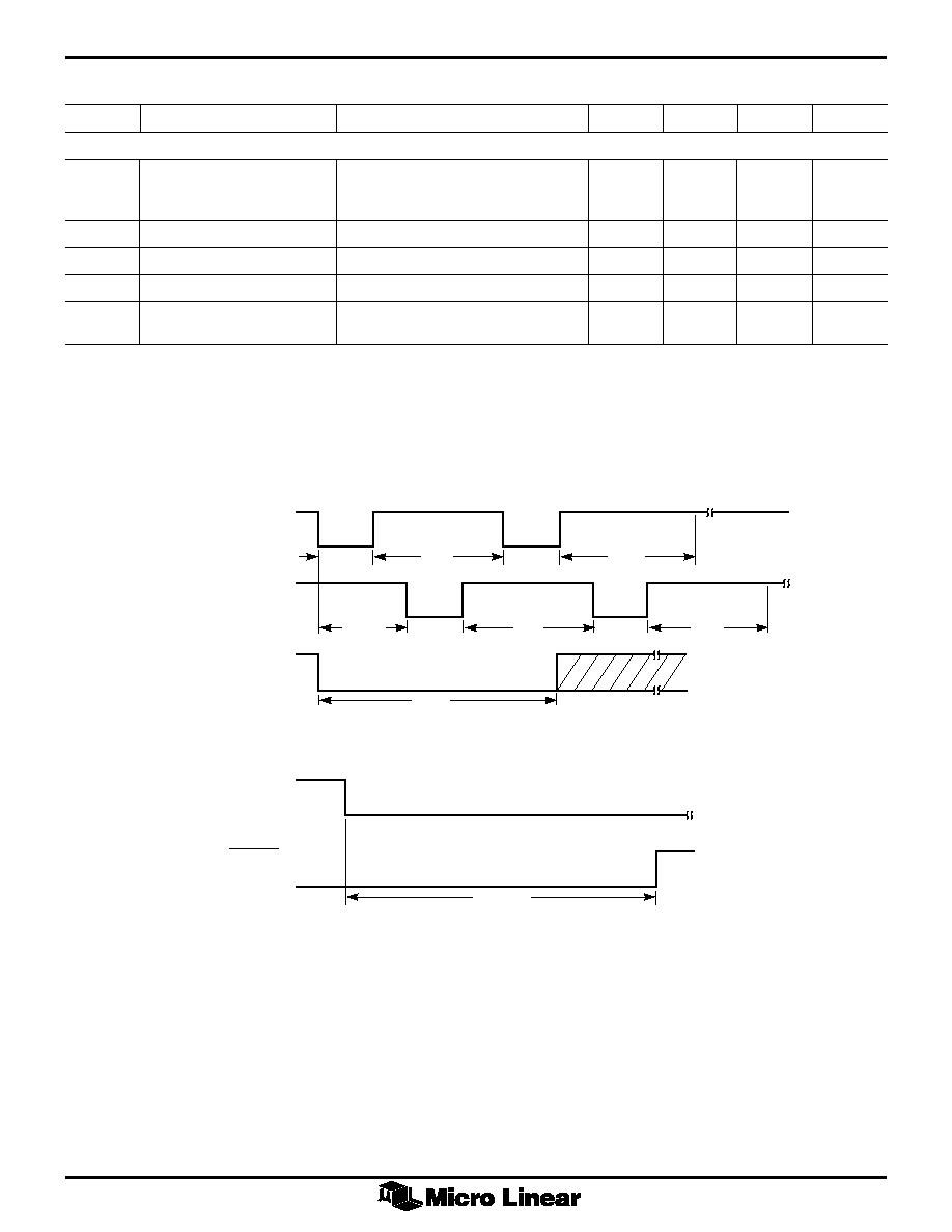
INSERTION AND BYPASS KEY GENERATION (Fig. 1)
T_K1
Key Element #1
808
858
�
s
(avg. P
O
< P
O_Off
)
T_K2
Key Element #2
1616
1717
�
s
(avg. P
O
> P
O_Off
)
T_K3
Key Element #3
1616
�
s
(avg. P
O
< P
O_Off
)
T_BYP
Bypass Element
4.85
26.5
ms
(avg. P
O
> P
O_Off
)
T_KINIT1
Time that phantom power
V(KEYGEN) = V
CC
, V(TPINOK) > 0.7V
26.5
ms
should be applied in config 1
before generating the insertion
key.
T_KINIT4
Time that the optical input
V(KEYGEN) = V
CC
, V(TPINOK) = 0V
26.5
ms
should be valid in config 4
V(PHTM1) = 0V, V(PHTM2) = 0V
before generating the insertion
key.
T_KOFF
Time that the optical input
V(KEYGEN) = VCC, V(TPINOK) = 0V
26.5
ms
should be invalid before
V(PHTM1) = 0V, V(PHTM2) = 0V
generating the bypass key.
ML6680
7
AC CHARACTERISTICS
(continued)
SYMBOL
PARAMETER
CONDITIONS
MIN
TYP
MAX
UNITS
INSERTION KEY ECHO AND BYPASS KEY RECOGNITION (Fig. 1)
T_ECHO
Time since starting insertion
100
ms
key generation until receiving
the insertion key echo.
T_E1Key
Key Echo From T_K1
766
900
�
s
T_E2Key
Key Echo From T_K2
1533
1800
�
s
T_E3Key
Key Echo From T_K3
1533
�
s
T_BYPDET Time of optical input not valid
4
4.5
ms
before recognizing a bypass key
GENERATED
INSERTION KEY
RECEIVED INSERTION
KEY ECHO
GENERATED
BYPASS KEY
RECEIVED
BYPASS KEY
INSERTED
T_K1
T_K1
T_K2
T_K3
T_ECHO
T_E1
T_E2
T_E3
T_BYP
T_BYPDET
T_E1
Figure 1
Note 1: Limits are guaranteed by 100% testing, sampling, or correlation with worst-case test conditions.
Note 2: Current into all V
CC
pins, external bias resistors, and external transmit loads. Does not include status LED's current.

ML6680
8
FUNCTIONAL DESCRIPTION
Fiber Optic LED Driver
The output stage of the transmitter is a current mode
switch which develops the output light by sinking current
from OPVCC through the LED into the OPOUT pin. Once
the current requirement for the LED is determined, the
RTSETOP resistor is selected. The following equation is
used to select the correct RTSETOP resistor:
RTSETOP = (52mA/I
OUT
)
�
115
No current is provided during the off cycles of the
Insertion, Bypass, or Echo Keys, or when the input signal
that should be routed to the Fiber Optic LED Driver does
not meet the corresponding input squelch requirements.
Fiber Optic Quantizer
The OPINP, OPINN input signal is fed into a limiting
amplifier with a gain of about 100 and input resistance of
1.3k
. Maximum sensitivity is achieved through the use
of a DC restoration feedback loop and AC coupling the
input. When AC coupled, the input DC bias voltage is set
by an on-chip network at about 1.7V. These coupling
capacitors, in conjunction with the input impedance of
the amplifier, establish a high pass filter with 3dB corner
frequency, f
L
, at
f
L
= 1/(2
�
�
1300
�
C)
Since the amplifier has a differential input, two capacitors
of equal value are required. If the signal driving the input
is single ended, one of the coupling capacitors can be tied
to V
CC
. The internal amplifier has a lowpass filter built-in
to band limit the input signal which in turn will improve
the signal to noise ratio. Although the input is AC coupled,
the offset voltage, V
OS
, within the amplifier will be present
at the amplifier's output. In order to reduce this error a DC
feedback loop nulls the offset voltage, forcing V
OS
to be
zero. The comparator is a high-speed differential zero
crossing detector that slices and accurately digitizes the
receive signal. The output of the comparator is fed in
parallel into both the fiber optic squelch circuit and the
signal MUX. The capacitor between pin VDC and QGND
should be set to 500pF.
Fiber Optic Squelch
The ML6680 monitors the frequency and amplitude of the
input from a fiberoptic receiver. The optical squelch
circuit rejects signals whose frequencies are lower than
1MHz or whose amplitudes are lower than �32dBm.
If both requirements are met, the LED output OPINOK
goes low, and the amplitude threshold is lowered 20%.
FREQUENCY OK
AMPLITUDE OK
SET
RESET
Q
OPINOK
Copper Pair Driver
The output stage of the twisted pair transmitter is a current
mode switch which develops the output voltage by driving
current through the terminating resistor and the output filter.
The harmonic content is controlled to simplify the filter
design. The transmitter employs a center tap 2:1 transformer
where the center tap is tied to V
CC
. While one pin of the
transmit pair is pulled low, the other pin floats. The output
pins to the twisted pair wires, TPOUTP and TPOUTN, can
drive shielded or unshielded twisted pair cable through the
appropriate isolation transformer. The output current is set
by the value of RTSETTP. No transitions are generated at
TPOUTP and TPOUTN when the input signal that should be
routed to the Copper Pair Driver does not meet the
corresponding input squelch requirements. PECL compatible
output are obtained with an external network of 3 resistors.
In this case the current of the output stage can be reduced
by adjusting the value of RTSETTP.
Twisted Pair Line Equalizer
The receive equalizer compensates for twisted pair cable
dispersion, which otherwise would give rise to inter-symbol
interference (ISI). The amount of equalization varies with the
average amplitude of the received signal. The received
signal amplitude gives a rough value for the length of the
attached cable. The filter/equalizer characteristic is the
inverse of the cable's dispersion characteristic. Both UTP
and STP cables approximate a low-pass filter, so the filter/
equalizer approximates an inverse square root equalizer.
Two external resistors and one external capacitors are
required between pins EQA and EQB. The output of the
equalizer is fed into the signal MUX. On a PECL application
these pins should be connected between each other.
Twisted Pair Squelch Circuit
The twisted pair line receiver internally sets the common
mode bias of the input TPINP and TPINN. Voltage offset
comparators are used to set the amplitude squelch
threshold, and analog timers are used to set the pulse width
squelch threshold. When the input signal meets amplitude
and pulse width requirements, the squelch circuit reduces
the offset voltage of the comparators, decreasing the
amplitude squelch threshold by half. This hysteresis allows
the receiver to stay on in the presence of a fading input
signal. The twisted pair squelch circuit rejects signals whose
frequencies are lower than 1MHz or whose amplitudes are
lower than 300mV
P-P
. If both requirements are met, the LED
output TPINOK goes low.
Clock Oscillator
The ML6680 provides an on-chip clock oscillator by
connecting a 32.768kHz watch crystal between pins
XTAL1 and XTAL2. The part can also be driven by an
external clock applied at XTAL1 and tying XTAL2 to
ground. The frequency of the external clock should be
between 32.7kHz and 34.5kHz.
Status LED Drivers
The ML6680 has three status LED drivers. The LED driver
pins are active low. The LED's are tied to their respective
pins through a 300
resistor to V
CC
.

ML6680
9
Modes of Operation
Four configurations are possible with the ML6680,
as follows:
1.Standard Media Converter: Senses ISO/IEC8802-5
phantom power and generates ISO/IEC8802-5
fiberoptic insertion or bypass requests.
2.Concentrator Media Converter: Recognizes the ISO/
IEC8802-5 fiberoptic insertion or bypass requests and
drives the ISO/IEC8802-5 phantom circuits.
3.Lobe or Ring Out Port Media Converter: Recognizes
the ISO/IEC8802-5 fiberoptic insertion or bypass
requests.
4.Ring In Port Media Converter: Generates ISO/
IEC8802-5 fiberoptic insertion or bypass requests.
Modifies the internal signal paths depending on the
presence or absence of a fiberoptic link, and on the
reception of the ISO/IEC8802-5 "Insertion Key Echo."
CONFIGURATION 1
Standard Media Converter:
This configuration is selected by tying KEYGEN to VCC.
There are always two fixed signal paths, one from TPINP and
TPINN to OPVCC and OPOUT, and another from OPINP
and OPINN to TPOUTP and TPOUTN. The generation of
the "Insertion Key" or "Bypass Key" is exclusively controlled
by the logic values at PHTM1 and PHTM2. The "Insertion
Key" is generated when both PHTM1 and PHTM2 go low,
and stay low for at least 26.5ms. If the "Insertion Key Echo"
is received within the following 100ms, the part goes to
the "Insert State" and the LED output INSERTED goes low.
During the generation of the "Insertion Key," and while
waiting for the "Insertion Key Echo" the states of PHTM1
and PHTM2 do not have any effect. When the part is in
the "Insert State" and either PHTM1 or PHTM2 goes high,
the LED output INSERTED goes high, the part leaves the
"Insert State," generates the "Bypass Key," and starts
waiting for PHTM1 and PHTM2 to go low again.
CONFIGURATION 2
Concentrator Media Converter:
This configuration is selected by tying KEYGEN to ground.
There are always two fixed signal paths, one from TPINP and
TPINN to OPVCC and OPOUT, and another from OPINP
and OPINN to TPOUTP and TPOUTN. The part powers
on in the "Bypass State" where it neither applies phantom
current nor checks for a phantom wire fault. After
recognizing an "Insertion Key" at its fiber optic inputs, it
applies phantom power by providing current at PHTM1 and
PHTM2, goes to the "Phantom Wire Fault Check State," and
starts waiting for a "Bypass Key." At this state, the LED output
INSERTED stays low while no phantom wire fault is
detected. When the part is in the "Phantom Wire Fault Check
State" and a "Bypass Key" is recognized, the part leaves
this state, removes the phantom power, and starts waiting
for a "Insertion Key" again.
CONFIGURATION 3
Lobe or Ring Out Port Media Converter:
This configuration is selected by tying both KEYGEN and
TPINOK to ground. When the ML6680 is in the "Insert
State," the signal paths are from TPINP and TPINN to
OPVCC and OPOUT, and from OPINP and OPINN to
TPOUTP and TPOUTN. Otherwise, the signal paths are
from TPINP and TPINN to TPOUTP and TPOUTN, and
from OPINP and OPINN to OPVCC and OPOUT. The part
powers on in the "Bypass State" and goes to the "Insert
State" after recognizing an "Insertion Key" at its fiber optic
inputs. It goes back to the "Bypass State" after recognizing
a "Bypass Key." While it is at the "Insert State," the LED
output INSERTED stays low.
CONFIGURATION 4
Ring In Port Media Converter:
This configuration is selected by tying KEYGEN to VCC
and TPINOK to ground. When the part is in the "Insert
State," the signal paths are from TPINP and TPINN to
OPVCC and OPOUT, and from OPINP and OPINN to
TPOUTP and TPOUTN. Otherwise, the input at TPINP
and TPINN is routed to TPOUTP and TPOUTN, and also
to OPVCC and OPOUT. The "Insertion Key" is generated
when activity is detected at OPINP and OPINN for at least
26.5ms and, PHTM1 and PHTM2 stay low. If the
"Insertion Key Echo" is received within the following
100ms, the ML6680 goes to the "Insert State" and the LED
output INSERTED goes low. During the generation of the
"Insertion Key," and while waiting for the "Insertion Key
Echo" the logic states of PHTM1 and PHTM2 do not have
any effect. When the part is in the "Insert State" and no
activity is detected at OPINP and OPINN for at least
26.5ms, or either PHTM1 or PHTM2 goes high, the LED
output INSERTED goes high, the part leaves the "Insert
State," generates the "Bypass Key," and starts waiting for
26.5ms of optical input activity again.
Low Frequency Signaling Mode
Some old implementations of discrete media converters,
use a non-standard protocol with frequencies between
1 and 10kHz. To facilitate the migration to the ML6680,
a specific operating mode is provided by grounding the
pin INSERTED. Pin KEYGEN should also be grounded to
prevent the generation of unwanted "Insertion" or "Bypass
Keys." In this operating mode, the optical frequency
squelch circuitry is disabled and the time constant of the
amplitude squelch is significantly reduced.
For each edge of the low frequency optical input, the
ML6680 generates a pulse at the led output OPINOK.
It also generates a pulse at the TPOUTP output for each
rising edge and another at the TPOUTN output for
each falling edge.

ML6680
10
Figure 2. ML6680 Configurations 1 and 2
OPINN
QGND
VDC
KEYGEN
GND1
OPGND
OPOUT
TPINP
TPINN
PHTM1
PHTM2
GND2
TPOUTP
TPOUTN
12
D3
D2
D1
R10
300
R6
300
R1
255
C7
0.1
�
F
R2
115
R3
1K
1414
U4
J2
C6
C21
0.1
�
F
0.1
�
F
10
0.1
�
F
0.1
�
F
C5
C4
R4
C13
50pF
C12
50pF
C14
220pF
C8
R14
R13
118
R19
4.7K
R15
698
10
C3
1nF
1nF
C2
R5
300
13
14
15
16
EQB
EQA
VCC2
XTAL1
XTAL2
QVCC
OPINP
TPINOK
RTSETTP
VCC1
INSERTED
RTSETOP
OPINOK
OPVCC
17
18
1
2
3
4
8
7
6
5
5
6
7
8
9
10
11
43
2
1
2
8
X2
32KHz
25
24
23
22
21
20
19
27
26
ML6680
U1
OC1
1
2
3
4
8
7
6
5
3
4
5
6
3
4
5
6
OC2
1
2
3
4
8
7
6
5
2416
U3
1
2
3
4
8
7
6
5
R17
4.7K
C19
C17
C18
L1
L2
4.7
�
H
4.7
�
H
J5
J4
C16
0.1
�
F
0.1
�
F
0.1
�
F
0.1
�
F
47
�
F4
7
�
F
R20
500
D4
C20
VCC
+5V
FVCC
FGND
C1
J1
1
2
3
4
R16
2.7K
R18
2.7K
5
6
7
8
16
15
T1
14
13
12
C15
R12
237
R11
237
11
10
9
U2
RJ45
3
4
5
6
3
4
5
6
RJ45
3
4
5
6
3
4
5
6
RJ45
CONFIG. 1
PHANTOM
SENSE
CONFIG. 2
PHANTOM
DRIVE
U1:
U2:
U3:
U4:
OC1:
X2:
T1:
D1-4:
ML6680
RJ45 CONNECTOR
HFBR2416 (HP) OR OP2416
(OPTEK) OPTICAL RECEIVER
HFBR1414 (HP) OR OP1414(OPTEK)
OPTICAL TRANSMITTER
MOTOROLA MOC217
32.768KHz CRYSTAL OSCILLATOR
TRANSFORMER MODULE,
VALOR SF1304 OR BEL S553�2793�03
LED, SURFACE MOUNT,
PANASONIC LN146IC-(TR)
CONFIGURATION ADJUSTMENTS:
STANDARD MEDIA CONVERTER CONFIGURATION 1:
REMOVE J4 AND J5 AND CONNECT J1 TO FVCC
CONCENTRATOR MEDIA CONVERTER CONFIGURATION 2:
CONNECT J4 AND J5, AND CONNECT J1 TO FGND.
REMOVE OC1, OC2, R16, R17, R18 AND R19
SHORT THE LOCATIONS OF PINS 2 AND 6 OF OC1
SHORT THE LOCATIONS OF PINS 2 AND 6 OF OC2
500pF
0.1
�
F
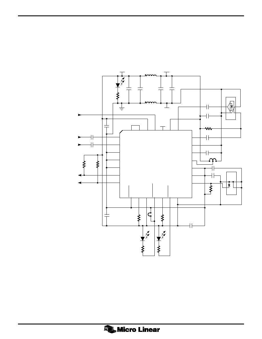
ML6680
11
Figure 3. ML6680 Configurations 3 and 4
OPINN
QGND
VDC
KEYGEN
GND1
OPGND
OPOUT
TPINP
TPINN
PHTM1
PHTM2
GND2
TPOUTP
TPOUTN
12
D2
D1
R6
300
R1
499
C7
R2
115
R3
1K
HFBR
U4
J2
C6
0.1
�
F
0.1
�
F
0.1
�
F
0.1
�
F
0.1
�
F
500pF
C21
C5
C4
R4
10
C3
C2
1nF
1nF
R5
300
13
14
15
16
EQB
EQA
VCC2
XTAL1
XTAL2
QVCC
OPINP
TPINOK
RTSETTP
VCC1
INSERTED
RTSETOP
OPINOK
OPVCC
17
18
1
2
3
4
8
7
6
5
5
6
7
8
9
10
11
4
3
2
1
28
NC
25
24
23
22
21
20
19
27
26
ML6680
U1
HFBR
2416
U3
1
2
3
4
8
7
6
5
C18
C17
47
�
F
47
�
F
L1
L2
4.7
�
H
4.7
�
H
R20
500
D4
C19
C20
0.1
�
F
0.1
�
F
25nF
25nF
0.1
�
F
VCC
+5V
FVCC
FGND
C1
J1
C10
R7
49.9
R8
49.9
C9
C8
COUTP
COUTN
CINP
CINN
U1:
U3:
U4:
D1, 2, 4:
ML6680
HFBR2416 (HP) OR OP2416
(OPTEK) OPTICAL RECEIVER
HFBR1414 (HP) OR OP1414 (OPTEK)
OPTICAL TRANSMITTERS
LED, SURFACE MOUNT,
PANASONIC LN146IC (TR)
CLOCK
CONFIGURATION 3: LOBE OR RING OUT PORT, J1 TO FGND
CONFIGURATION 4: RING IN PORT, J1 TO FVCC
FROM THE UPSTREAM
LOBE PORT IN CONFIG. 3
FROM THE UPSTREAM
RING OUT PORT IN
CONFIG. 4
TO THE DOWNSTREAM
RING IN PORT IN CONFIG. 3
TO THE DOWNSTREAM LOBE
PORT IN CONFIG. 4

ML6680
12
ORDERING INFORMATION
PART NUMBER
TEMPERATURE RANGE
PACKAGE
ML668
0CQ 0
�
C to 70
�
C
28-PIN PLCC (Q28)
Micro Linear reserves the right to make changes to any product herein to improve reliability, function or design.
Micro Linear does not assume any liability arising out of the application or use of any product described herein,
neither does it convey any license under its patent right nor the rights of others. The circuits contained in this
data sheet are offered as possible applications only. Micro Linear makes no warranties or representations as to
whether the illustrated circuits infringe any intellectual property rights of others, and will accept no responsibility
or liability for use of any application herein. The customer is urged to consult with appropriate legal counsel
before deciding on a particular application.
DS6680-01
2092 Concourse Drive
San Jose, CA 95131
Tel: 408/433-5200
Fax: 408/432-0295
� Micro Linear 1997
is a registered trademark of Micro Linear Corporation
Products described in this document may be covered by one or more of the following patents, U.S.: 4,897,611; 4,964,026; 5,027,116; 5,281,862; 5,283,483; 5,418,502; 5,508,570; 5,510,727; 5,523,940;
5,546,017; 5,559,470; 5,565,761; 5,592,128; 5,594,376; Japan: 2598946; 2619299. Other patents are pending.
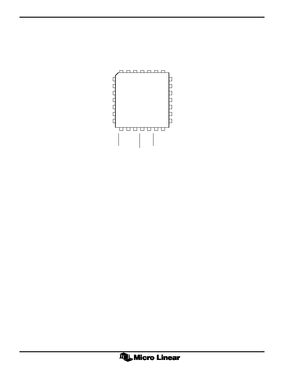
PHYSICAL DIMENSIONS
inches (millimeters)
0.099 - 0.110
(2.51 - 2.79)
PIN 1 ID
SEATING PLANE
0.485 - 0.495
(12.32 - 12.57)
0.450 - 0.456
(11.43 - 11.58)
0.013 - 0.021
(0.33 - 0.53)
0.165 - 0.180
(4.06 - 4.57)
1
0.450 - 0.456
(11.43 - 11.58)
0.485 - 0.495
(12.32 - 12.57)
8
15
22
0.025 - 0.045
(0.63 - 1.14)
(RADIUS)
0.050 BSC
(1.27 BSC)
0.009 - 0.011
(0.23 - 0.28)
0.026 - 0.032
(0.66 - 0.81)
0.042 - 0.048
(1.07 - 1.22)
0.148 - 0.156
(3.76 - 3.96)
0.042 - 0.056
(1.07 - 1.42)
0.390 - 0.430
(9.90 - 10.92)
0.300 BSC
(7.62 BSC)
Package: Q28
28-Pin PLCC