 | ÐлекÑÑоннÑй компоненÑ: MCP13xx | СкаÑаÑÑ:  PDF PDF  ZIP ZIP |
21985a.book
© 2005 Microchip Technology Inc.
DS21985A-page 1
MCP131X/2X
Features
· Low supply current: 1 A (typ.), 10 A (max.)
· Precision monitoring trip point options:
- 2.9V and 4.6V (Standard Offerings)
- 2.0V to 4.7V in 100 mV increments,
(Contact the local Microchip Sales Office)
· Resets microcontroller in a power-loss event
· Reset Delay Time Out Option:
- 1.4 ms, 30 ms, 200 ms, or 1.6s (typ.)
· Watchdog Timer Input Time Out Options:
- 6.3 ms, 102 ms, 1.6s or 25.6s (typ.)
· Manual Reset (MR) input (active-low)
· Single and complementary Reset output(s)
· Reset Output Options:
- Push-Pull (active-high or active-low)
- Open-Drain (internal or external Pull-up)
· Temperature Range: -40°C to +125°C
· Voltage Range: 1.0V to 5.5V
· Lead Free Packaging
Description
The MCP1316/16M/17/18/18M/19/19M/20/21/22 are
voltage supervisor devices designed to keep a micro-
controller in Reset until the system voltage has reached
and stabilized at the proper level for reliable system
operation. This sevice family also offers a Watchdog
Timer to monitor system operation and a Manual Reset
input. The table below shows the available features for
these devices.
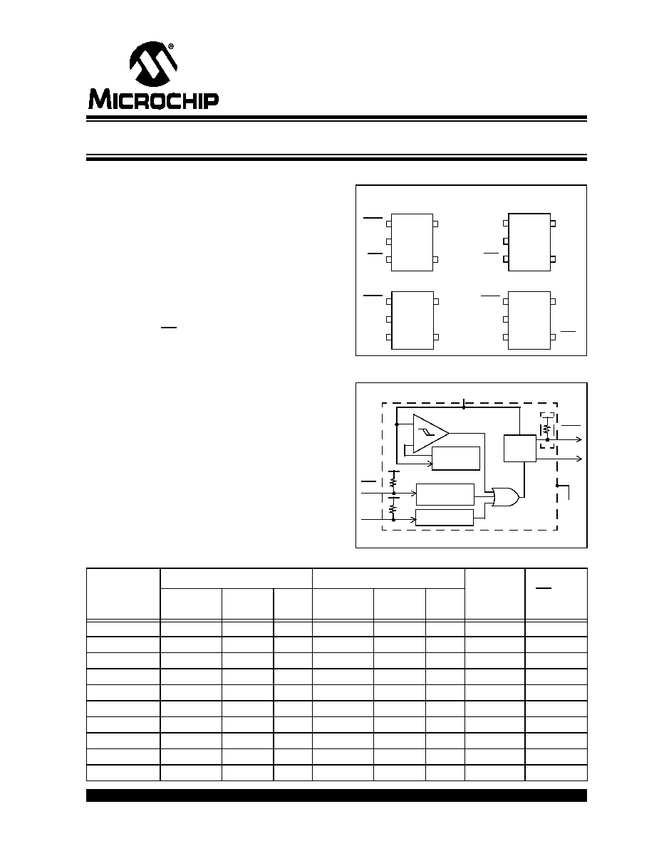
Package Types
Block Diagram
Device Features
1
2
3
5
4
MCP1317
1
2
3
5
4
MCP1318/18M/21
1
2
3
5
4
MCP1319/19M/22
1
2
3
5
4
MCP1316/16M/20
SOT-23-5
RST
RST
V
SS
MR
WDI
V
DD
V
DD
RST
V
SS
MR
WDI
V
SS
RST
WDI
V
DD
RST
V
SS
RST
MR
V
DD
V
DD
Comparator
+
Output
Driver
RST
Reference
V
SS
RST
Noise Filter
Watchdog
MR
WDI
Note: Features available depend on the device
Voltage
Device
Reset Output A
Reset Output B
WDI Input
MR Input
Type
Pull-up
Resistor
Active
Level
Type
Pull-up
Resistor
Active
Level
MCP1316
Push-Pull
--
Low
--
--
--
Yes
Yes
MCP1316M
Open-Drain
Internal
Low
--
--
--
Yes
Yes
MCP1317
Push-Pull
--
High
--
--
--
Yes
Yes
MCP1318
Push-Pull
--
Low
Push-Pull
--
High
Yes
No
MCP1318M
Open-Drain
Internal
Low
Push-Pull
--
High
Yes
No
MCP1319
Push-Pull
--
Low
Push-Pull
--
High
No
Yes
MCP1319M
Open-Drain
Internal
Low
Push-Pull
--
High
No
Yes
MCP1320
Open-Drain
External
Low
--
--
--
Yes
Yes
MCP1321
Open-Drain
External
Low
Push-Pull
--
High
Yes
No
MCP1322
Open-Drain
External
Low
Push-Pull
--
High
No
Yes
Voltage Supervisor
MCP131X/2X
DS21985A-page 2
© 2005 Microchip Technology Inc.
1.0
ELECTRICAL
CHARACTERISTICS
Absolute Maximum Ratings
Supply Voltage (V
DD
to V
SS
) . . . . . . . . . . . . . . . . . . . . . . 7.0V
Input current (V
DD
) . . . . . . . . . . . . . . . . . . . . . . . . . . . .10 mA
Output current (RST) . . . . . . . . . . . . . . . . . . . . . . . . . .10 mA
Voltage on all inputs and outputs, except Open-Drain RST
(with no internal pull-up resistor), w.r.t. V
SS
. . . . . . . . . . . . . . . . . . . . . . . . . . . . . . . -0.6V to (V
DD
+ 1.0V)
Voltage on Open-Drain RST
(with no internal pull-up resistor) w.r.t. V
SS
. . -0.6V to 13.5V
Storage temperature . . . . . . . . . . . . . . . . . . .-65°C to +150°C
Ambient temp. with power applied . . . . . . . .-40°C to +125°C
Maximum Junction temp. with power applied . . . . . . . . 150°C
Power Dissipation (T
A
70°C):
5-Pin SOT-23A .......................................................240 mW
ESD protection on all pins
..................................................
4 kV
Notice: Stresses above those listed under "Maximum Rat-
ings" may cause permanent damage to the device. This is a
stress rating only and functional operation of the device at
those or any other conditions above those indicated in the
operational listings of this specification is not implied. Expo-
sure to maximum rating conditions for extended periods may
affect device reliability.
DC CHARACTERISTICS
Electrical Specifications: Unless otherwise indicated, all limits are specified for V
DD
= 1V to 5.5V, R
PU
= 100 k
(only MCP1320, MCP1321 and MCP1322), T
A
= -40°C to +125°C.
Parameters
Sym
Min
Typ
Max
Units
Conditions
Operating Voltage Range
V
DD
1.0
--
5.5
V
Specified V
DD
Value to V
OUT
Low
V
DD
1.0
--
--
V
I
RST
= 10 A, V
RST
< 0.3V
Operating Current:
I
DD
--
5
10
A
Watchdog Timer Active
--
1
2
A
Watchdog Timer Inactive
--
1
2
A
V
DD
< V
TRIP
--
5
10
A
Reset Delay Timer Active
Note 1:
Trip point is ±1.5% from typical value.
2:
Trip point is ±2.5% from typical value.
3:
Hysterysis is minimum = 1%, max = 6% at +25°C.
4:
This specification allows this device to be used in PICmicro
®
microcontroller applications that require the
In-Circuit Serial ProgrammingTM (ICSPTM) feature (see device-specific programming specifications for
voltage requirements). The total time that the RST pin can be above the maximum device operational volt-
age (5.5V) is 100s. Current into the RST pin should be limited to 2 mA. It is recommended that the device
operational temperature be maintained between 0°C to +70°C (+25°C preferred). For additional informa-
tion, refer to Figure 2-35.
5:
This parameter is established by characterization and is not 100% tested.
6:
Custom ordered voltage trip point; minimum order volume requirement. Information available upon request.
© 2005 Microchip Technology Inc.
DS21985A-page 3
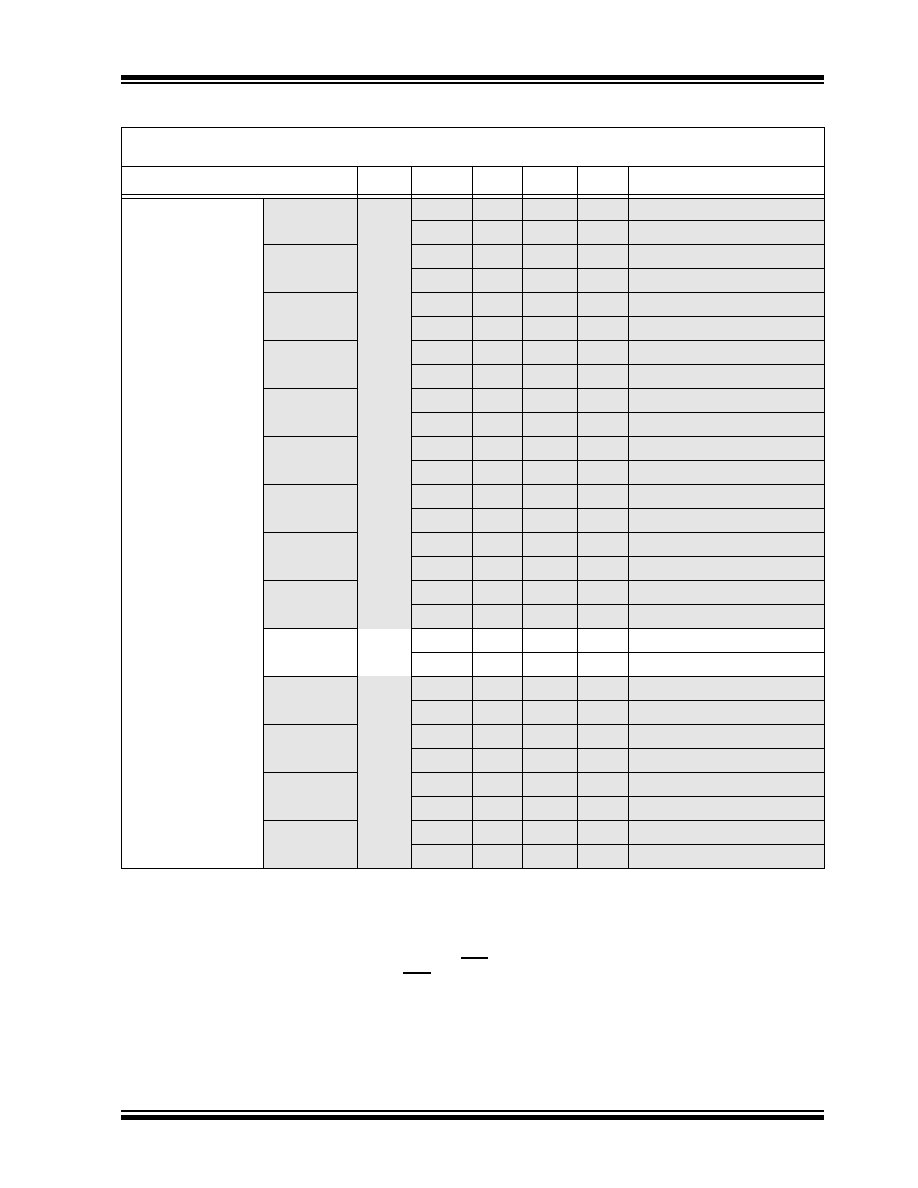
MCP131X/2X
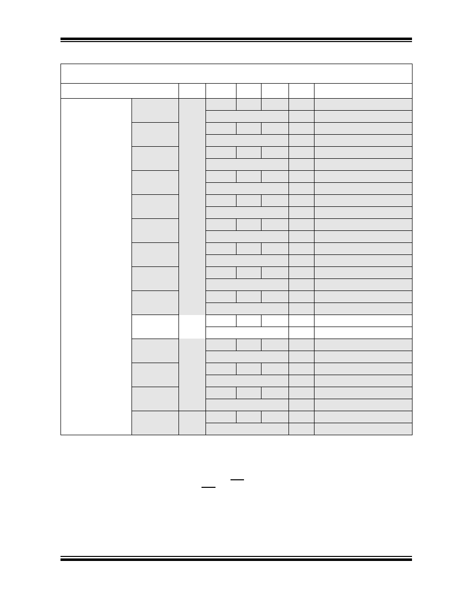
V
DD
Trip Point
MCP13XX-20
V
TRIP
1.970
2.00
2.030
V
T
A
= +25°C (Note 1)
(Note 6)
1.950
2.00
2.050
V
T
A
= -40°C to +85°C (Note 2)
MCP13XX-21
2.069
2.10
2.132
V
T
A
= +25°C (Note 1)
(Note 6)
2.048
2.10
2.153
V
T
A
= -40°C to +85°C (Note 2)
MCP13XX-22
2.167
2.20
2.233
V
T
A
= +25°C (Note 1)
(Note 6)
2.145
2.20
2.255
V
T
A
= -40°C to +85°C (Note 2)
MCP13XX-23
2.266
2.30
2.335
V
T
A
= +25°C (Note 1)
(Note 6)
2.243
2.30
2.358
V
T
A
= -40°C to +85°C (Note 2)
MCP13XX-24
2.364
2.40
2.436
V
T
A
= +25°C (Note 1)
(Note 6)
2.340
2.40
2.460
V
T
A
= -40°C to +85°C (Note 2)
MCP13XX-25
2.463
2.50
2.538
V
T
A
= +25°C (Note 1)
(Note 6)
2.438
2.50
2.563
V
T
A
= -40°C to +125°C (Note 2)
MCP13XX-26
2.561
2.60
2.639
V
T
A
= +25°C (Note 1)
(Note 6)
2.535
2.60
2.665
V
T
A
= -40°C to +125°C (Note 2)
MCP13XX-27
2.660
2.70
2.741
V
T
A
= +25°C (Note 1)
(Note 6)
2.633
2.70
2.768
V
T
A
= -40°C to +125°C (Note 2)
MCP13XX-28
2.758
2.80
2.842
V
T
A
= +25°C (Note 1)
(Note 6)
2.730
2.80
2.870
V
T
A
= -40°C to +125°C (Note 2)
MCP13XX-29
2.857
2.90
2.944
V
T
A
= +25°C (Note 1)
2.828
2.90
2.973
V
T
A
= -40°C to +125°C (Note 2)
MCP13XX-30
2.955
3.00
3.045
V
T
A
= +25°C (Note 1)
(Note 6)
2.925
3.00
3.075
V
T
A
= -40°C to +125°C (Note 2)
MCP13XX-31
3.054
3.10
3.147
V
T
A
= +25°C (Note 1)
(Note 6)
3.023
3.10
3.178
V
T
A
= -40°C to +125°C (Note 2)
MCP13XX-32
3.152
3.20
3.248
V
T
A
= +25°C (Note 1)
(Note 6)
3.120
3.20
3.280
V
T
A
= -40°C to +125°C (Note 2)
MCP13XX-33
3.251
3.30
3.350
V
T
A
= +25°C (Note 1)
(Note 6)
3.218
3.30
3.383
V
T
A
= -40°C to +125°C (Note 2)
DC CHARACTERISTICS (CONTINUED)
Electrical Specifications: Unless otherwise indicated, all limits are specified for V
DD
= 1V to 5.5V, R
PU
= 100 k
(only MCP1320, MCP1321 and MCP1322), T
A
= -40°C to +125°C.
Parameters
Sym
Min
Typ
Max
Units
Conditions
Note 1:
Trip point is ±1.5% from typical value.
2:
Trip point is ±2.5% from typical value.
3:
Hysterysis is minimum = 1%, max = 6% at +25°C.
4:
This specification allows this device to be used in PICmicro
®
microcontroller applications that require the
In-Circuit Serial ProgrammingTM (ICSPTM) feature (see device-specific programming specifications for
voltage requirements). The total time that the RST pin can be above the maximum device operational volt-
age (5.5V) is 100s. Current into the RST pin should be limited to 2 mA. It is recommended that the device
operational temperature be maintained between 0°C to +70°C (+25°C preferred). For additional informa-
tion, refer to Figure 2-35.
5:
This parameter is established by characterization and is not 100% tested.
6:
Custom ordered voltage trip point; minimum order volume requirement. Information available upon request.
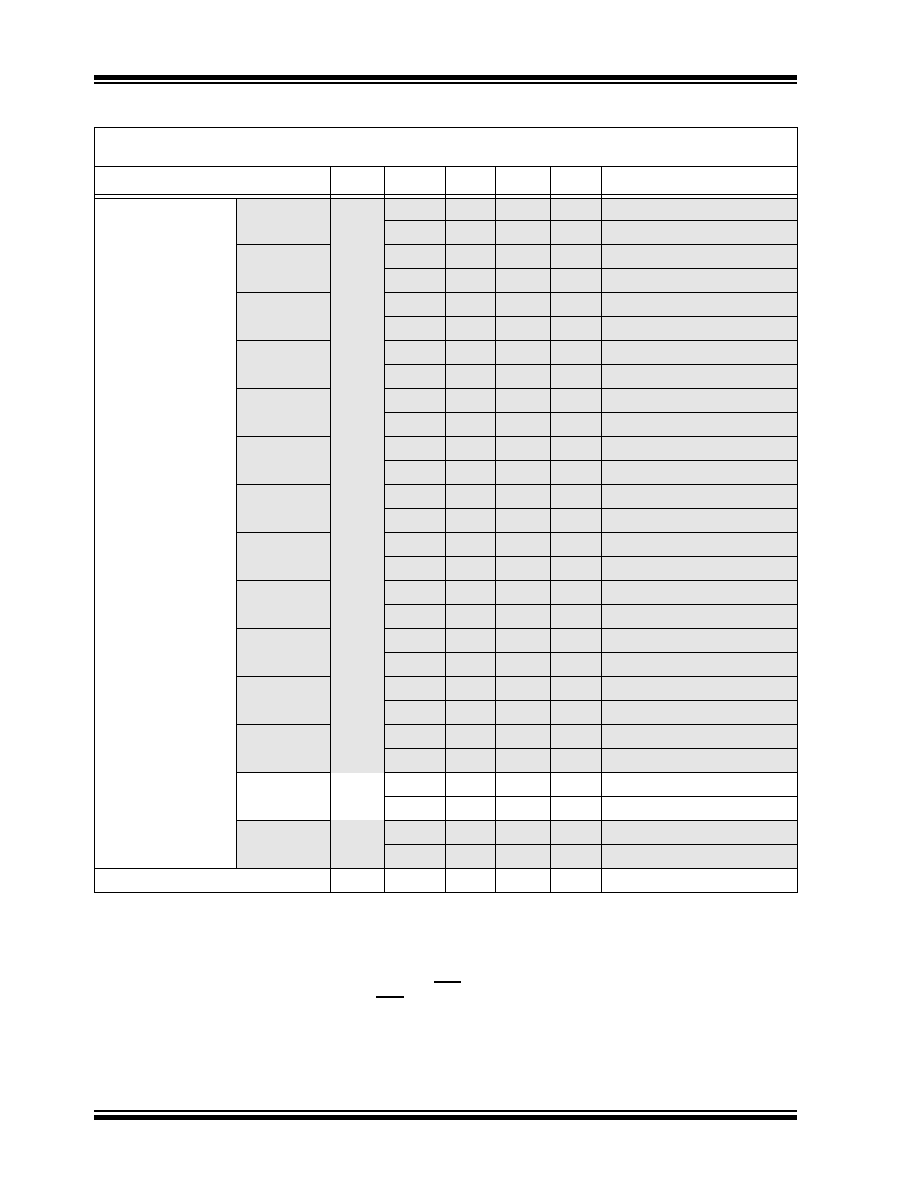
MCP131X/2X
DS21985A-page 4
© 2005 Microchip Technology Inc.
V
DD
Trip Point (Con't) MCP13XX-34
V
TRIP
3.349
3.40
3.451
V
T
A
= +25°C (Note 1)
(Note 6)
3.315
3.40
3.385
V
T
A
= -40°C to +125°C (Note 2)
MCP13XX-35
3.448
3.50
3.553
V
T
A
= +25°C (Note 1)
(Note 6)
3.413
3.50
3.588
V
T
A
= -40°C to +125°C (Note 2)
MCP13XX-36
3.546
3.60
3.654
V
T
A
= +25°C (Note 1)
(Note 6)
3.510
3.60
3.690
V
T
A
= -40°C to +125°C (Note 2)
MCP13XX-37
3.645
3.70
3.756
V
T
A
= +25°C (Note 1)
(Note 6)
3.608
3.70
3.793
V
T
A
= -40°C to +125°C (Note 2)
MCP13XX-38
3.743
3.80
3.857
V
T
A
= +25°C (Note 1)
(Note 6)
3.705
3.80
3.895
V
T
A
= -40°C to +125°C (Note 2)
MCP13XX-39
3.842
3.90
3.959
V
T
A
= +25°C (Note 1)
(Note 6)
3.803
3.90
3.998
V
T
A
= -40°C to +125°C (Note 2)
MCP13XX-40
3.940
4.00
4.060
V
T
A
= +25°C (Note 1)
(Note 6)
3.900
4.00
4.100
V
T
A
= -40°C to +125°C (Note 2)
MCP13XX-41
4.039
4.10
4.162
V
T
A
= +25°C (Note 1)
(Note 6)
3.998
4.10
4.203
V
T
A
= -40°C to +125°C (Note 2)
MCP13XX-42
4.137
4.20
4.263
V
T
A
= +25°C (Note 1)
(Note 6)
4.095
4.20
4.305
V
T
A
= -40°C to +125°C (Note 2)
MCP13XX-43
4.236
4.30
4.365
V
T
A
= +25°C (Note 1)
(Note 6)
4.193
4.30
4.408
V
T
A
= -40°C to +125°C (Note 2)
MCP13XX-44
4.334
4.40
4.466
V
T
A
= +25°C (Note 1)
(Note 6)
4.290
4.40
4.510
V
T
A
= -40°C to +125°C (Note 2)
MCP13XX-45
4.433
4.50
4.568
V
T
A
= +25°C (Note 1)
(Note 6)
4.388
4.50
4.613
V
T
A
= -40°C to +125°C (Note 2)
MCP13XX-46
4.531
4.60
4.669
V
T
A
= +25°C (Note 1)
4.485
4.60
4.715
V
T
A
= -40°C to +125°C (Note 2)
MCP13XX-47
4.630
4.70
4.771
V
T
A
= +25°C (Note 1)
(Note 6)
4.583
4.70
4.818
V
T
A
= -40°C to +125°C (Note 2)
V
DD
Trip Point Tempco
T
TPCO
--
±40
--
ppm/°C
DC CHARACTERISTICS (CONTINUED)
Electrical Specifications: Unless otherwise indicated, all limits are specified for V
DD
= 1V to 5.5V, R
PU
= 100 k
(only MCP1320, MCP1321 and MCP1322), T
A
= -40°C to +125°C.
Parameters
Sym
Min
Typ
Max
Units
Conditions
Note 1:
Trip point is ±1.5% from typical value.
2:
Trip point is ±2.5% from typical value.
3:
Hysterysis is minimum = 1%, max = 6% at +25°C.
4:
This specification allows this device to be used in PICmicro
®
microcontroller applications that require the
In-Circuit Serial ProgrammingTM (ICSPTM) feature (see device-specific programming specifications for
voltage requirements). The total time that the RST pin can be above the maximum device operational volt-
age (5.5V) is 100s. Current into the RST pin should be limited to 2 mA. It is recommended that the device
operational temperature be maintained between 0°C to +70°C (+25°C preferred). For additional informa-
tion, refer to Figure 2-35.
5:
This parameter is established by characterization and is not 100% tested.
6:
Custom ordered voltage trip point; minimum order volume requirement. Information available upon request.
© 2005 Microchip Technology Inc.
DS21985A-page 5
MCP131X/2X
Threshold Hysteresis
MCP13XX-20
V
HYS
0.020
--
0.120
V
T
A
= +25°C (Note 3)
(
Note 3)
(Note 6)
(Note 6)
V
T
A
= -40°C to +85°C
MCP13XX-21
0.021
--
0.126
V
T
A
= +25°C (Note 3)
(Note 6)
(Note 6)
V
T
A
= -40°C to +85°C
MCP13XX-22
0.022
--
0.132
V
T
A
= +25°C (Note 3)
(Note 6)
(Note 6)
V
T
A
= -40°C to +85°C
MCP13XX-23
0.023
--
0.138
V
T
A
= +25°C (Note 3)
(Note 6)
(Note 6)
V
T
A
= -40°C to +85°C
MCP13XX-24
0.024
--
0.144
V
T
A
= +25°C (Note 3)
(Note 6)
(Note 6)
V
T
A
= -40°C to +85°C
MCP13XX-25
0.025
--
0.150
V
T
A
= +25°C (Note 3)
(Note 6)
(Note 6)
V
T
A
= -40°C to +125°C
MCP13XX-26
0.026
--
0.156
V
T
A
= +25°C (Note 3)
(Note 6)
(Note 6)
V
T
A
= -40°C to +125°C
MCP13XX-27
0.027
--
0.162
V
T
A
= +25°C (Note 3)
(Note 6)
(Note 6)
V
T
A
= -40°C to +125°C
MCP13XX-28
0.028
--
0.168
V
T
A
= +25°C (Note 3)
(Note 6)
(Note 6)
V
T
A
= -40°C to +125°C
MCP13XX-29
0.029
--
0.174
V
T
A
= +25°C (Note 3)
(Note 6)
V
T
A
= -40°C to +125°C
MCP13XX-30
0.030
--
0.180
V
T
A
= +25°C (Note 3)
(Note 6)
(Note 6)
V
T
A
= -40°C to +125°C
MCP13XX-31
0.031
--
0.186
V
T
A
= +25°C (Note 3)
(Note 6)
(Note 6)
V
T
A
= -40°C to +125°C
MCP13XX-32
0.032
--
0.192
V
T
A
= +25°C (Note 3)
(Note 6)
(Note 6)
V
T
A
= -40°C to +125°C
MCP13XX-33
V
HYS
0.033
--
0.198
V
T
A
= +25°C (Note 3)
(Note 6)
(Note 6)
V
T
A
= -40°C to +125°C
DC CHARACTERISTICS (CONTINUED)
Electrical Specifications: Unless otherwise indicated, all limits are specified for V
DD
= 1V to 5.5V, R
PU
= 100 k
(only MCP1320, MCP1321 and MCP1322), T
A
= -40°C to +125°C.
Parameters
Sym
Min
Typ
Max
Units
Conditions
Note 1:
Trip point is ±1.5% from typical value.
2:
Trip point is ±2.5% from typical value.
3:
Hysterysis is minimum = 1%, max = 6% at +25°C.
4:
This specification allows this device to be used in PICmicro
®
microcontroller applications that require the
In-Circuit Serial ProgrammingTM (ICSPTM) feature (see device-specific programming specifications for
voltage requirements). The total time that the RST pin can be above the maximum device operational volt-
age (5.5V) is 100s. Current into the RST pin should be limited to 2 mA. It is recommended that the device
operational temperature be maintained between 0°C to +70°C (+25°C preferred). For additional informa-
tion, refer to Figure 2-35.
5:
This parameter is established by characterization and is not 100% tested.
6:
Custom ordered voltage trip point; minimum order volume requirement. Information available upon request.
Document Outline