2000 Microchip Technology Inc.
Preliminary
DS21291C-page 1
MCP2510
FEATURES
� Implements Full CAN V2.0A and V2.0B at 1 Mb/s
- 0 - 8 byte message length
- Standard and extended data frames
- Programmable bit rate up to 1 Mb/s
- Support for remote frames
- Two receive buffers with prioritized message
storage
- Six full acceptance filters
- Two full acceptance filter masks
- Three transmit buffers with prioritization and
abort features
- Loop-back mode for self test operation
� Hardware Features
- High Speed SPI Interface
(5 MHz at 4.5V I temp)
- Supports SPI modes 0,0 and 1,1
- Clock out pin with programmable prescaler
- Interrupt output pin with selectable enables
- `Buffer full' output pins configureable as inter-
rupt pins for each receive buffer or as general
purpose digital outputs
- `Request to Send' input pins configureable as
control pins to request immediate message
transmission for each transmit buffer or as
general purpose digital inputs
- Low Power Sleep mode
� Low power CMOS technology
- Operates from 3.0V to 5.5V
- 5 mA active current typical
- 10
�
A standby current typical at 5.5V
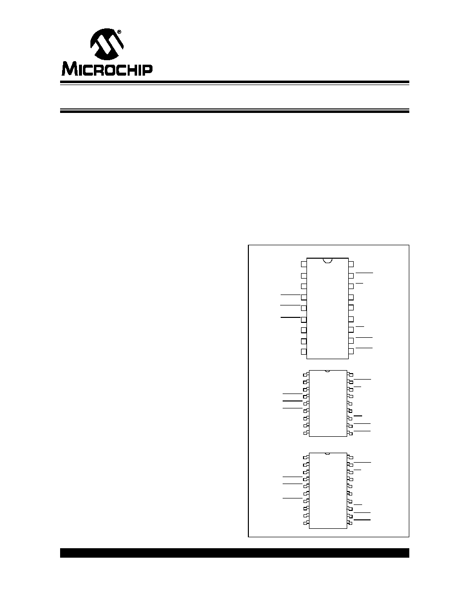
� 18-pin PDIP/SOIC and 20-pin TSSOP packages
� Temperature ranges supported:
DESCRIPTION
The Microchip Technology Inc. MCP2510 is a Full Con-
troller Area Network (CAN) protocol controller imple-
menting CAN specification V2.0 A/B. It supports CAN
1.2, CAN 2.0A, CAN 2.0B Passive, and CAN 2.0B
Active versions of the protocol, and is capable of trans-
mitting and receiving standard and extended messages.
It is also capable of both acceptance filtering and mes-
sage management. It includes three transmit buffers and
two receive buffers that reduce the amount of microcon-
troller (MCU) management required. The MCU commu-
nication is implemented via an industry standard Serial
Peripheral Interface (SPI) with data rates up to 5Mb/s.
PACKAGE TYPES
- Industrial (I):
-40�C to +85�C
- Extended (E):
-40�C to +125�C
18 LEAD PDIP
TXCAN
RXCAN
V
DD
RESET
CS
SO
MC
P2
510
1
2
3
4
18
17
16
15
SI
SCK
INT
RX0BF
14
13
12
11
RX1BF
10
OSC2
OSC1
CLKOUT
TX2RTS
5
6
7
8
Vss
9
MC
P2
510
TXCAN
RXCAN
TX0RTS
OSC1
CLKOUT
OSC2
CS
V
DD
RESET
SO
SCK
INT
SI
RX0BF
RX1BF
Vss
TX0RTS
TX1RTS
TX1RTS
TX2RTS
18 LEAD SOIC
MC
P2
510
TXCAN
RXCAN
TX0RTS
OSC1
CLKOUT
OSC2
CS
V
DD
RESET
SO
SCK
INT
SI
RX0BF
RX1BF
Vss
11
10
TX1RTS
TX2RTS
20 LEAD TSSOP
NC
NC
1
2
3
4
5
6
7
8
9
18
17
16
15
14
13
12
13
12
1
2
3
4
5
6
7
8
9
20
19
18
17
16
15
14
11
10
Stand-Alone CAN Controller with SPI
TM
Interface
SPI is a registered trademark of Motorola Inc.

MCP2510
DS21291C-page 2
Preliminary
2000 Microchip Technology Inc.
Table of Contents
1.0
Device Functionality . . . . . . . . . . . . . . . . . . . . . . . . . . . . . . . . . . . . . . . . . . . . . . . . . . . . . . . . . . . . . . . . . . . . . . . . . . . . . . . 3
2.0
Can Message Frames. . . . . . . . . . . . . . . . . . . . . . . . . . . . . . . . . . . . . . . . . . . . . . . . . . . . . . . . . . . . . . . . . . . . . . . . . . . . . . 7
3.0
Message Transmission . . . . . . . . . . . . . . . . . . . . . . . . . . . . . . . . . . . . . . . . . . . . . . . . . . . . . . . . . . . . . . . . . . . . . . . . . . . . 15
4.0
Message Reception . . . . . . . . . . . . . . . . . . . . . . . . . . . . . . . . . . . . . . . . . . . . . . . . . . . . . . . . . . . . . . . . . . . . . . . . . . . . . . 21
5.0
Bit Timing . . . . . . . . . . . . . . . . . . . . . . . . . . . . . . . . . . . . . . . . . . . . . . . . . . . . . . . . . . . . . . . . . . . . . . . . . . . . . . . . . . . . . . 35
6.0
Error Detection . . . . . . . . . . . . . . . . . . . . . . . . . . . . . . . . . . . . . . . . . . . . . . . . . . . . . . . . . . . . . . . . . . . . . . . . . . . . . . . . . . 41
7.0
Interrupts. . . . . . . . . . . . . . . . . . . . . . . . . . . . . . . . . . . . . . . . . . . . . . . . . . . . . . . . . . . . . . . . . . . . . . . . . . . . . . . . . . . . . . . 45
8.0
Oscillator . . . . . . . . . . . . . . . . . . . . . . . . . . . . . . . . . . . . . . . . . . . . . . . . . . . . . . . . . . . . . . . . . . . . . . . . . . . . . . . . . . . . . . . 49
9.0
Modes of Operation . . . . . . . . . . . . . . . . . . . . . . . . . . . . . . . . . . . . . . . . . . . . . . . . . . . . . . . . . . . . . . . . . . . . . . . . . . . . . . 51
10.0
Register Map. . . . . . . . . . . . . . . . . . . . . . . . . . . . . . . . . . . . . . . . . . . . . . . . . . . . . . . . . . . . . . . . . . . . . . . . . . . . . . . . . . . . 55
11.0
SPI Interface . . . . . . . . . . . . . . . . . . . . . . . . . . . . . . . . . . . . . . . . . . . . . . . . . . . . . . . . . . . . . . . . . . . . . . . . . . . . . . . . . . . . 57
12.0
Electrical Characteristics. . . . . . . . . . . . . . . . . . . . . . . . . . . . . . . . . . . . . . . . . . . . . . . . . . . . . . . . . . . . . . . . . . . . . . . . . . . 61
13.0
Packaging Information . . . . . . . . . . . . . . . . . . . . . . . . . . . . . . . . . . . . . . . . . . . . . . . . . . . . . . . . . . . . . . . . . . . . . . . . . . . . 65
On-Line Support . . . . . . . . . . . . . . . . . . . . . . . . . . . . . . . . . . . . . . . . . . . . . . . . . . . . . . . . . . . . . . . . . . . . . . . . . . . . . . . . . . . . . . . . . 69
Reader Response . . . . . . . . . . . . . . . . . . . . . . . . . . . . . . . . . . . . . . . . . . . . . . . . . . . . . . . . . . . . . . . . . . . . . . . . . . . . . . . . . . . . . . . . 70
MCP2510 Product Identification System. . . . . . . . . . . . . . . . . . . . . . . . . . . . . . . . . . . . . . . . . . . . . . . . . . . . . . . . . . . . . . . . . . . . . . . 71
Index . . . . . . . . . . . . . . . . . . . . . . . . . . . . . . . . . . . . . . . . . . . . . . . . . . . . . . . . . . . . . . . . . . . . . . . . . . . . . . . . . . . . . . . . . . . . . . . . . . 73
List Of Figures. . . . . . . . . . . . . . . . . . . . . . . . . . . . . . . . . . . . . . . . . . . . . . . . . . . . . . . . . . . . . . . . . . . . . . . . . . . . . . . . . . . . . . . . . . . 75
List Of Tables . . . . . . . . . . . . . . . . . . . . . . . . . . . . . . . . . . . . . . . . . . . . . . . . . . . . . . . . . . . . . . . . . . . . . . . . . . . . . . . . . . . . . . . . . . . 75
List Of Registers . . . . . . . . . . . . . . . . . . . . . . . . . . . . . . . . . . . . . . . . . . . . . . . . . . . . . . . . . . . . . . . . . . . . . . . . . . . . . . . . . . . . . . . . . 75
Worldwide Sales and Service . . . . . . . . . . . . . . . . . . . . . . . . . . . . . . . . . . . . . . . . . . . . . . . . . . . . . . . . . . . . . . . . . . . . . . . . . . . . . . . 76
To Our Valued Customers
Most Current Data Sheet
To obtain the most up-to-date version of this data sheet, please check our Worldwide Web site at:
http://www.microchip.com
You can determine the version of a data sheet by examining its literature number found on the bottom outside corner of any page.
The last character of the literature number is the version number. e.g., DS30000A is version A of document DS30000.
Errata
An errata sheet may exist for current devices, describing minor operational differences (from the data sheet) and recommended
workarounds. As device/documentation issues become known to us, we will publish an errata sheet. The errata will specify the
revision of silicon and revision of document to which it applies.
To determine if an errata sheet exists for a particular device, please check with one of the following:
� Microchip's Worldwide Web site; http://www.microchip.com
� Your local Microchip sales office (see last page)
� The Microchip Corporate Literature Center; U.S. FAX: (480) 792-7277
When contacting a sales office or the literature center, please specify which device, revision of silicon and data sheet (include lit-
erature number) you are using.
Corrections to this Data Sheet
We constantly strive to improve the quality of all our products and documentation. We have spent a great deal of time to ensure
that this document is correct. However, we realize that we may have missed a few things. If you find any information that is missing
or appears in error, please:
� Fill out and mail in the reader response form in the back of this data sheet.
� E-mail us at webmaster@microchip.com.
We appreciate your assistance in making this a better document.

2000 Microchip Technology Inc.
Preliminary
DS21291C-page 3
MCP2510
1.0
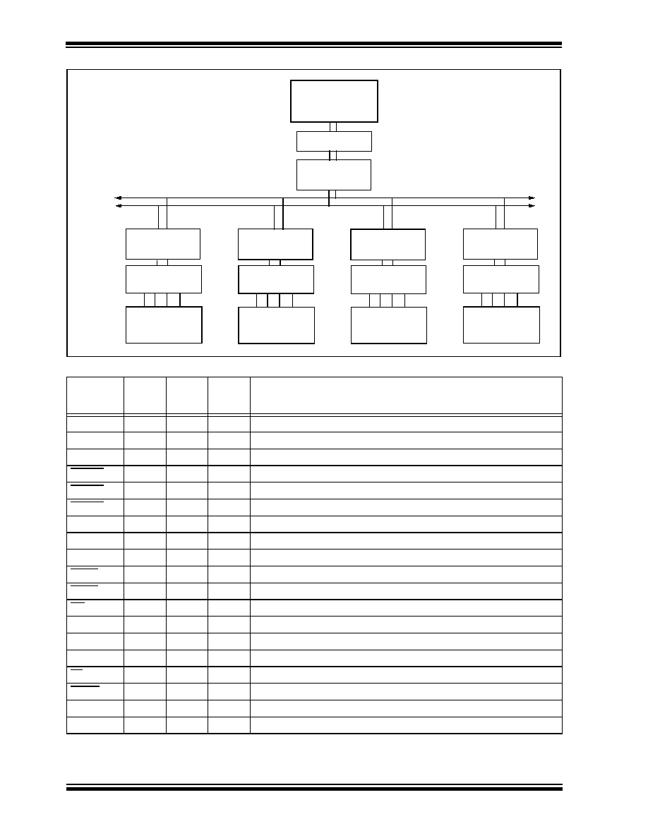
DEVICE FUNCTIONALITY
1.1
Overview
The MCP2510 is a stand-alone CAN controller devel-
oped to simplify applications that require interfacing
with a CAN bus. A simple block diagram of the
MCP2510 is shown in Figure 1-1. The device consists
of three main blocks:
1.
the CAN protocol engine,
2.
the control logic and SRAM registers that are
used to configure the device and its operation,
and
3.
the SPI protocol block.
A typical system implementation using the device is
shown in Figure 1-2.
The CAN protocol engine handles all functions for
receiving and transmitting messages on the bus. Mes-
sages are transmitted by first loading the appropriate
message buffer and control registers. Transmission is
initiated by using control register bits, via the SPI inter-
face, or by using the transmit enable pins. Status and
errors can be checked by reading the appropriate reg-
isters. Any message detected on the CAN bus is
checked for errors and then matched against the user
defined filters to see if it should be moved into one of
the two receive buffers.
The MCU interfaces to the device via the SPI interface.
Writing to and reading from all registers is done using
standard SPI read and write commands.
Interrupt pins are provided to allow greater system flex-
ibility. There is one multi-purpose interrupt pin as well
as specific interrupt pins for each of the receive regis-
ters that can be used to indicate when a valid message
has been received and loaded into one of the receive
buffers. Use of the specific interrupt pins is optional,
and the general purpose interrupt pin as well as status
registers (accessed via the SPI interface) can also be
used to determine when a valid message has been
received.
There are also three pins available to initiate immediate
transmission of a message that has been loaded into
one of the three transmit registers. Use of these pins is
optional and initiating message transmission can also
be done by utilizing control registers accessed via the
SPI interface.
Table 1-1 gives a complete list of all of the pins on the
MCP2510.
FIGURE 1-1:
Block Diagram
3 TX
Buffers
2 RX Buffers
Message Assembly
6 Acceptance
Filters
SPI
Interface
Logic
SPI
Bus
INT
Buffer
CS
SCK
SI
SO
CAN
Protocol
Engine
RXCAN
TXCAN
Control Logic
RX0BF
RX1BF
TX0RTS
TX1RTS
TX2RTS
MCP2510
DS21291C-page 4
Preliminary
2000 Microchip Technology Inc.
FIGURE 1-2:
Typical System Implementation
TABLE 1-1:
Pin Descriptions
Name
DIP/
SOIC
Pin #
TSSOP
Pin #
I/O/P
Type
Description
TXCAN
1
1
O
Transmit output pin to CAN bus
RXCAN
2
2
I
Receive input pin from CAN bus
CLKOUT
3
3
O
Clock output pin with programmable prescaler
TX0RTS
4
4
I
Transmit buffer TXB0 request to send or general purpose digital input. -100K
TX1RTS
5
5
I
Transmit buffer TXB1 request to send or general purpose digital input. -100K
TX2RTS
6
7
I
Transmit buffer TXB2 request to send or general purpose digital input. -100K
OSC2
7
8
O
Oscillator output
OSC1
8
9
I
Oscillator input
V
SS
9
10
P
Ground reference for logic and I/O pins
RX1BF
10
11
O
Receive buffer RXB1 interrupt pin or general purpose digital output
RX0BF
11
12
O
Receive buffer RXB0 interrupt pin or general purpose digital output
INT
12
13
O
Interrupt output pin
SCK
13
14
I
Clock input pin for SPI interface
SI
14
16
I
Data input pin for SPI interface
SO
15
17
O
Data output pin for SPI interface
CS
16
18
I
Chip select input pin for SPI interface
RESET
17
19
I
Active low device reset input
V
DD
18
20
P
Positive supply for logic and I/O pins
NC
--
6,15
--
No internal connection
Note:
Type Identification: I=Input; O=Output; P=Power
MCP2510
SPI
MCP2510
MCP2510
MCP2510
INTERFACE
CAN
BUS
MCP2510
CAN
Transceiver
Node
Controller
Main
System
Controller
CAN
Transceiver
CAN
Transceiver
CAN
Transceiver
CAN
Transceiver
Node
Controller
Node
Controller
Node
Controller

2000 Microchip Technology Inc.
Preliminary
DS21291C-page 5
MCP2510
1.2
Transmit/Receive Buffers
The MCP2510 has three transmit and two receive buffers, two acceptance masks (one for each receive buffer), and a
total of six acceptance filters. Figure 1-3 is a block diagram of these buffers and their connection to the protocol engine.
FIGURE 1-3:
CAN Buffers and Protocol Engine Block Diagram
Acceptance Filter
RXF2
R
X
B
1
Identifier
Data Field
Data Field
Identifier
Acceptance Mask
RXM1
Acceptance Filter
RXF3
Acceptance Filter
RXF4
Acceptance Filter
RXF5
M
A
B
Acceptance Filter
RXF0
Acceptance Filter
RXF1
R
X
B
0
TXR
E
Q
TXB2
AB
T
F
ML
O
A
TXE
R
R
M
ESSA
G
E
Message
Queue
Control
Transmit Byte Sequencer
TXR
E
Q
TXB0
AB
T
F
ML
O
A
TXE
R
R
M
ESSA
G
E
CRC<14:0>
Comparator
Receive<7:0>
Transmit<7:0>
Receive
Error
Transmit
Error
Protocol
REC
TEC
ErrPas
BusOff
Finite
State
Machine
Counter
Counter
Shift<14:0>
{Transmit<5:0>, Receive<8:0>}
Transmit
Logic
Bit
Timing
Logic
TX
RX
Configuration
Registers
Clock
Generator
PROTOCOL
ENGINE
BUFFERS
TX
R
E
Q
TXB1
AB
T
F
ML
O
A
TXE
R
R
M
ESSA
G
E
A
c
c
e
p
t
Acceptance Mask
RXM0
A
c
c
e
p
t