 | –≠–ª–µ–∫—Ç—Ä–æ–Ω–Ω—ã–π –∫–æ–º–ø–æ–Ω–µ–Ω—Ç: MCP3304 | –°–∫–∞—á–∞—Ç—å:  PDF PDF  ZIP ZIP |
2002 Microchip Technology Inc.
DS21697B-page 1
M
MCP3302/04
Features
∑ Full Differential Inputs
∑ MCP3302: 2 Differential or 4 Single ended Inputs
∑ MCP3304: 4 Differential or 8 Single ended Inputs
∑ ±1 LSB max DNL
∑ ±1 LSB max INL (MCP3302/04-B)
∑ ±2 LSB max INL (MCP3302/04-C)
∑ Single supply operation: 2.7V to 5.5V
∑ 100 ksps sampling rate with 5V supply voltage
∑ 50 ksps sampling rate with 2.7V supply voltage
∑ 50 nA typical standby current, 1
µ
A max
∑ 450
µ
A max active current at 5V
∑ Industrial temp range: -40∞C to +85∞C
∑ 14 and 16-pin PDIP, SOIC and TSSOP packages
∑ MXDEV
TM
Evaluation kit available
Applications
∑ Remote Sensors
∑ Battery Operated Systems
∑ Transducer Interface
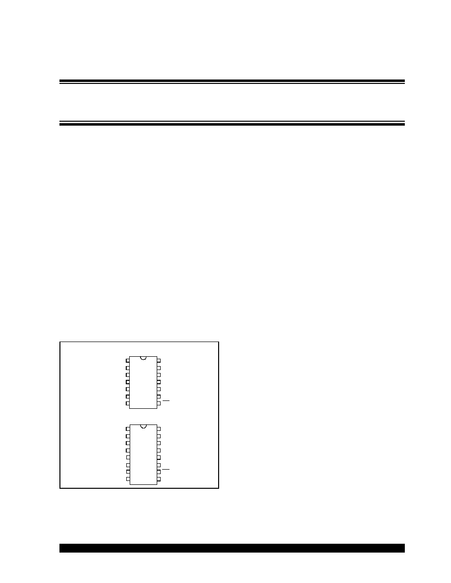
Package Types
General Description
The Microchip Technology Inc. MCP3302/04 13-bit A/D
converters feature full differential inputs and low power
consumption in a small package that is ideal for battery
powered systems and remote data acquisition applica-
tions. The MCP3302 is programmable to provide two
differential input pairs or four single ended inputs. The
MCP3304 is programmable and provides four differen-
tial input pairs or eight single ended inputs.
Incorporating a successive approximation architecture
with on-board sample and hold circuitry, these 13-bit
A/D converters are specified to have ±1 LSB Differen-
tial Nonlinearity (DNL); ±1 LSB Integral Nonlinearity
(INL) for B-grade and ±2 LSB for C-grade devices. The
industry-standard SPITM serial interface enables 13-bit
A/D converter capability to be added to any PICmicro
Æ
microcontroller.
The MCP3302/04 devices feature low current design
that permits operation with typical standby and active
currents of only 50 nA and 300
µ
A, respectively. The
devices operate over a broad voltage range of 2.7V to
5.5V and are capable of conversion rates of up to
100 ksps. The reference voltage can be varied from
400 mV to 5V, yielding input-referred resolution
between 98
µ
V and 1.22 mV.
The MCP3302 is available in 14-pin PDIP, 150 mil
SOIC and TSSOP packages. The MCP3304 is avail-
able in 16-pin PDIP and 150 mil SOIC packages. The
full differential inputs of these devices enable a wide
variety of signals to be used in applications such as
remote data acquisition, portable instrumentation and
battery operated applications.
V
DD
CLK
D
OUT
MCP3
3
0
2
1
2
3
4
14
13
12
11
10
9
8
5
6
7
V
REF
D
IN
CH0
CH1
CH2
CH3
CS/SHDN
DGND
AGND
NC
V
DD
CLK
D
OUT
M
C
P3304
1
2
3
4
16
15
14
13
12
11
10
9
5
6
7
8
V
REF
D
IN
CS/SHDN
DGND
CH0
CH1
CH2
CH3
CH4
CH5
CH6
CH7
NC
AGND
PDIP, SOIC, TSSOP
PDIP, SOIC
13-Bit Differential Input, Low Power A/D Converter
with SPITM Serial Interface
MCP3302/04
DS21697B-page 2
2002 Microchip Technology Inc.
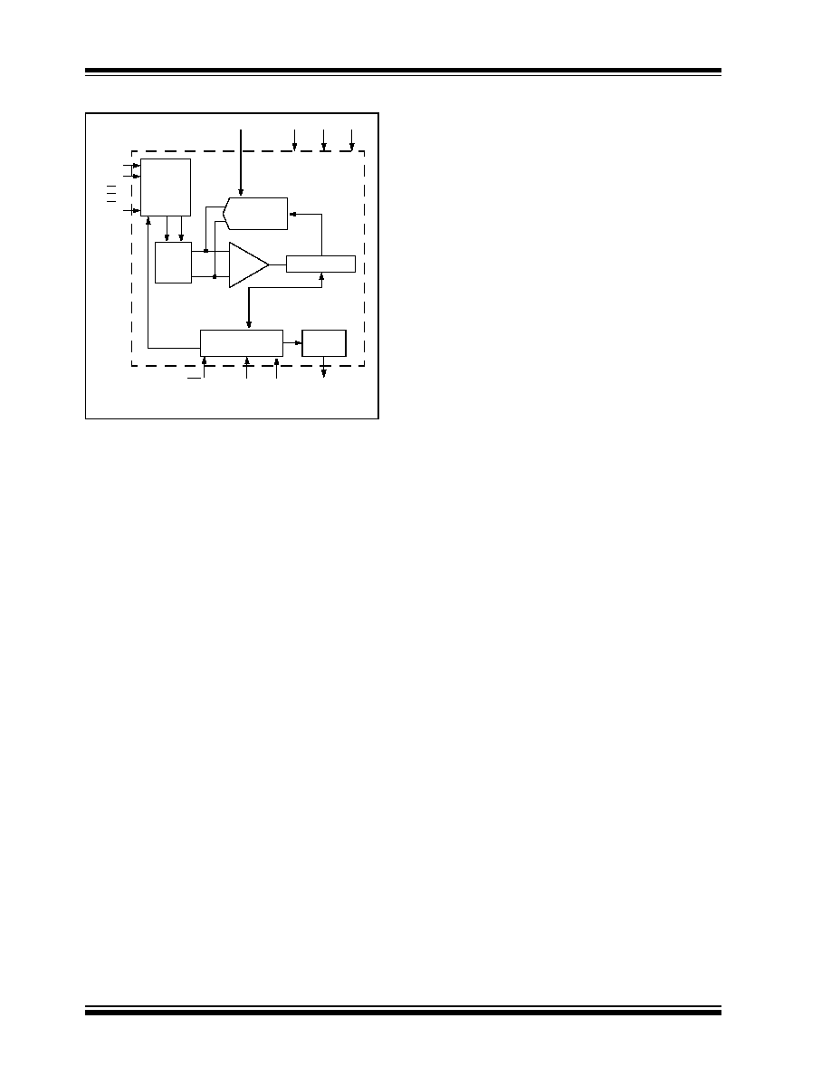
Functional Block Diagram
Comparator
13-Bit SAR
CDAC
Control Logic
CS/SHDN
V
REF
AGND
V
DD
CLK
D
OUT
Shift
Register
CH0
Channel
Mux
Input
CH1
CH7*
* Channels 5-7 available on MCP3304 Only
D
IN
+
-
& Hold
Circuits
Sample
DGND
2002 Microchip Technology Inc.
DS21697B-page 3
MCP3302/04
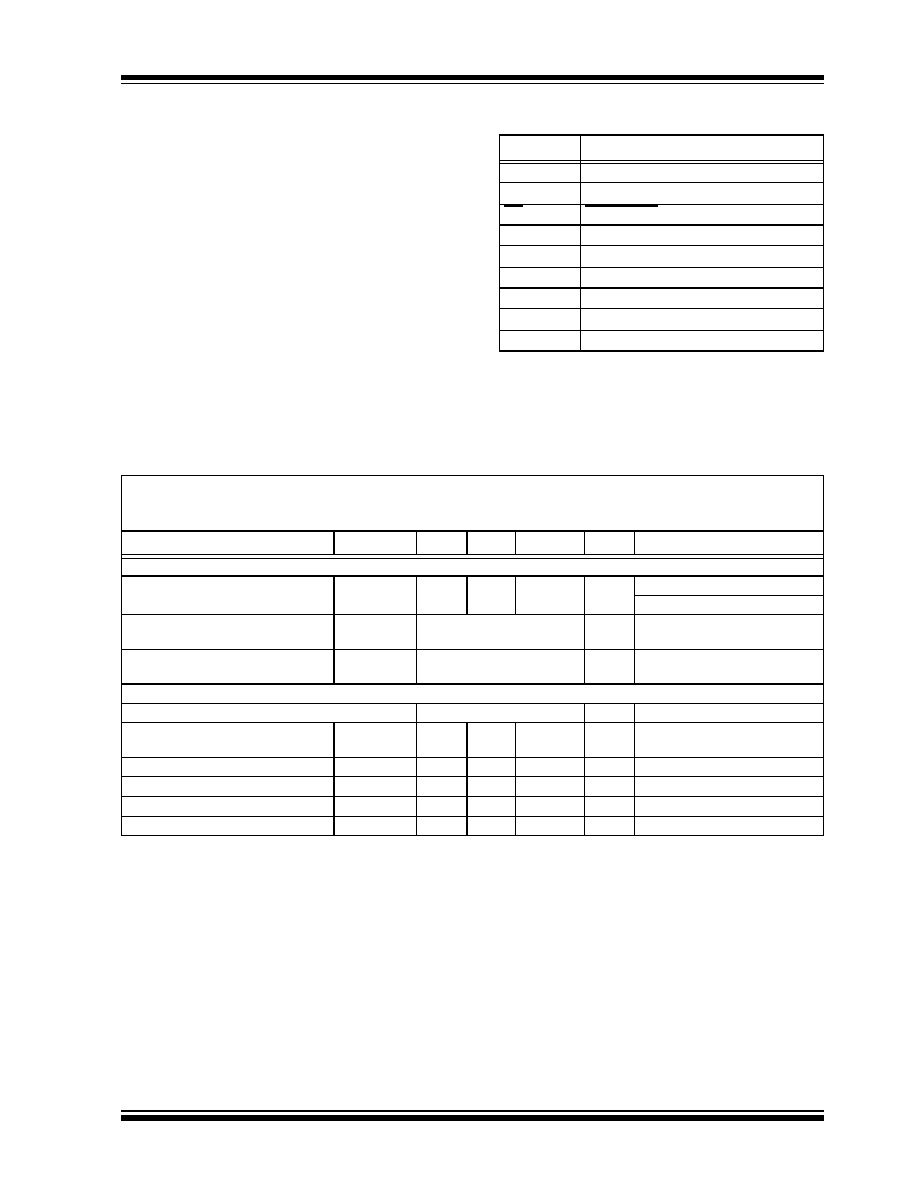
1.0
ELECTRICAL
CHARACTERISTICS
Maximum Ratings*
V
DD
........................................................................ 7.0V
All inputs and outputs w.r.t. V
SS
.....-0.3V to V
DD
+0.3V
Storage temperature .......................... -65∞C to +150∞C
Ambient temp. with power applied ..... -65∞C to +125∞C
Maximum Junction Temperature ....................... 150∞C
ESD protection on all pins (HBM)
......................... >
4 kV
*Notice: Stresses above those listed under "Maximum rat-
ings" may cause permanent damage to the device. This is a
stress rating only and functional operation of the device at
those or any other conditions above those indicated in the
operational listings of this specification is not implied. Expo-
sure to maximum rating conditions for extended periods may
affect device reliability.
PIN FUNCTION TABLE
Name
Function
CH0-CH7
Analog Inputs
DGND
Digital Ground
CS/SHDN
Chip Select / Shutdown Input
D
IN
Serial Data In
D
OUT
Serial Data Out
CLK
Serial Clock
AGND
Analog Ground
V
REF
Reference Voltage Input
V
DD
+2.7V to 5.5V Power Supply
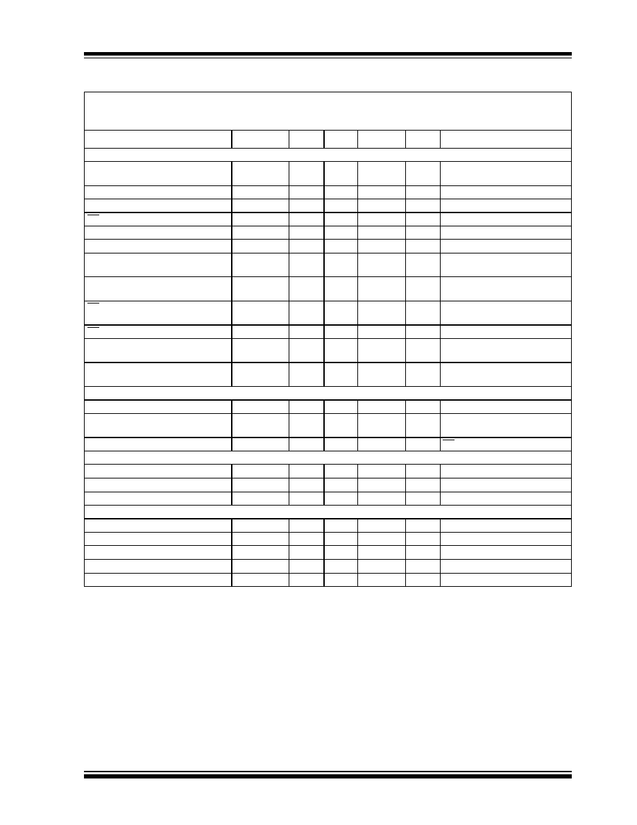
ELECTRICAL SPECIFICATIONS
Electrical Characteristics: Unless otherwise noted, all parameters apply at V
DD
= 5V, V
SS
= 0V, and V
REF
= 5V. Full differential
input configuration (Figure 3-4) with fixed common mode voltage of 2.5V. All parameters apply over temperature with
T
AMB
= -40∞C to +85∞C (Note 7). Conversion speed (F
SAMPLE
) is 100 ksps with F
CLK
= 21*F
SAMPLE
Parameter
Symbol
Min
Typ
Max
Units
Conditions
Conversion Rate
Maximum Sampling Frequency
F
SAMPLE
--
--
100
ksps
Note 8
--
--
50
ksps
V
DD
= V
REF
= 2.7V, V
CM
=1.35V
Conversion Time
T
CONV
13
CLK
periods
Acquisition Time
T
ACQ
1.5
CLK
periods
DC Accuracy
Resolution
12 data bits + sign
bits
Integral Nonlinearity
INL
--
--
±0.5
±1
±1
±2
LSB
LSB
MCP3302/04-B
MCP3302/04-C
Differential Nonlinearity
DNL
--
±0.5
±1
LSB
Monotonic over temperature
Positive Gain Error
-3
-0.75
+2
LSB
Negative Gain Error
-3
-0.5
+2
LSB
Offset Error
-3
+3
+6
LSB
Note 1: This specification is established by characterization and not 100% tested.
2: See characterization graphs that relate converter performance to V
REF
level.
3: V
IN
= 0.1V to 4.9V @ 1 kHz.
4: V
DD
=5V
P-P
±500 mV @ 1 kHz, see test circuit Figure 3-3.
5: Maximum clock frequency specification must be met.
6: V
REF
= 400 mV, V
IN
= 0.1V to 4.9V @ 1 kHz
7: TSSOP devices are only specified at 25∞C and +85∞C.
8: For slow sample rates, see Section 6.2.1 for limitations on clock frequency.
MCP3302/04
DS21697B-page 4
2002 Microchip Technology Inc.
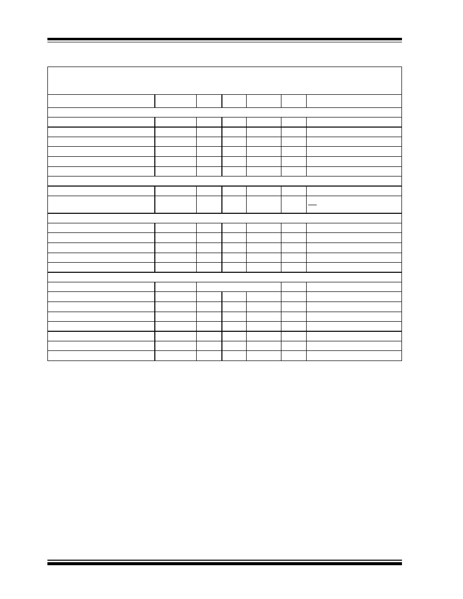
Dynamic Performance
Total Harmonic Distortion
THD
--
-91
--
dB
Note 3
Signal to Noise and Distortion
SINAD
--
78
--
dB
Note 3
Spurious Free Dynamic Range
SFDR
--
92
--
dB
Note 3
Common Mode Rejection
CMRR
--
79
--
dB
Note 6
Channel to Channel Crosstalk
CT
--
> -110
--
dB
Note 6
Power Supply Rejection
PSR
--
74
--
dB
Note 4
Reference Input
Voltage Range
0.4
--
V
DD
V
Note 2
Current Drain
--
--
100
0.001
150
3
µ
A
µ
A
CS = V
DD
= 5V
Analog Inputs
Full Scale Input Span
CH0 - CH7
-V
REF
--
V
REF
V
Absolute Input Voltage
CH0 - CH7
-0.3
--
V
DD
+ 0.3
V
Leakage Current
--
0.001
±1
µ
A
Switch Resistance
R
S
--
1
--
k
See Figure 6-3
Sample Capacitor
C
SAMPLE
--
25
--
pF
See Figure 6-3
Digital Input/Output
Data Coding Format
Binary Two's Complement
High Level Input Voltage
V
IH
0.7 V
DD
--
--
V
Low Level Input Voltage
V
IL
--
--
0.3 V
DD
V
High Level Output Voltage
V
OH
4.1
--
--
V
I
OH
= -1 mA, V
DD
= 4.5V
Low Level Output Voltage
V
OL
--
--
0.4
V
I
OL
= 1 mA, V
DD
= 4.5V
Input Leakage Current
I
LI
-10
--
10
µ
A
V
IN
= V
SS
or V
DD
Output Leakage Current
I
LO
-10
--
10
µ
A
V
OUT
= V
SS
or V
DD
Pin Capacitance
C
IN
, C
OUT
--
--
10
pF
T
AMB
= 25∞C, F = 1 MHz, Note 1
ELECTRICAL SPECIFICATIONS (CONTINUED)
Electrical Characteristics: Unless otherwise noted, all parameters apply at V
DD
= 5V, V
SS
= 0V, and V
REF
= 5V. Full differential
input configuration (Figure 3-4) with fixed common mode voltage of 2.5V. All parameters apply over temperature with
T
AMB
= -40∞C to +85∞C (Note 7). Conversion speed (F
SAMPLE
) is 100 ksps with F
CLK
= 21*F
SAMPLE
Parameter
Symbol
Min
Typ
Max
Units
Conditions
Note 1: This specification is established by characterization and not 100% tested.
2: See characterization graphs that relate converter performance to V
REF
level.
3: V
IN
= 0.1V to 4.9V @ 1 kHz.
4: V
DD
=5V
P-P
±500 mV @ 1 kHz, see test circuit Figure 3-3.
5: Maximum clock frequency specification must be met.
6: V
REF
= 400 mV, V
IN
= 0.1V to 4.9V @ 1 kHz
7: TSSOP devices are only specified at 25∞C and +85∞C.
8: For slow sample rates, see Section 6.2.1 for limitations on clock frequency.
2002 Microchip Technology Inc.
DS21697B-page 5
MCP3302/04
Timing Specifications:
Clock Frequency (Note 8)
F
CLK
0.105
0.105
--
--
2.1
1.05
MHz
MHz
V
DD
= 5V, F
SAMPLE
= 100 ksps
V
DD
= 2.7V, F
SAMPLE
= 50 ksps
Clock High Time
T
HI
210
--
--
ns
Note 5
Clock Low Time
T
LO
210
--
--
ns
Note 5
CS Fall To First Rising CLK Edge
T
SUCS
100
--
--
ns
Data In Setup time
T
SU
50
--
--
ns
Data In Hold Time
T
HD
--
--
50
ns
CLK Fall To Output Data Valid
T
DO
--
--
125
200
ns
ns
V
DD
= 5V, see Figure 3-1
V
DD
= 2.7V, see Figure 3-1
CLK Fall To Output Enable
T
EN
--
--
125
200
ns
ns
V
DD
= 5V, see Figure 3-1
V
DD
= 2.7V, see Figure 3-1
CS Rise To Output Disable
T
DIS
--
--
100
ns
See test circuits, Figure 3-1
Note 1
CS Disable Time
T
CSH
475
--
--
ns
D
OUT
Rise Time
T
R
--
--
100
ns
See test circuits, Figure 3-1
Note 1
D
OUT
Fall Time
T
F
--
--
100
ns
See test circuits, Figure 3-1
Note 1
Power Requirements:
Operating Voltage
V
DD
2.7
--
5.5
V
Operating Current
I
DD
--
--
300
200
450
--
µ
A
V
DD
, V
REF
= 5V, D
OUT
unloaded
V
DD
, V
REF
= 2.7V, D
OUT
unloaded
Standby Current
I
DDS
--
0.05
1
µ
A
CS = V
DD
= 5.0V
Temperature Ranges:
Specified Temperature Range
T
A
-40
--
+85
∞C
Operating Temperature Range
T
A
-40
--
+85
∞C
Storage Temperature Range
T
A
-65
--
+150
∞C
Thermal Package Resistance:
Thermal Resistance, 14L-PDIP
JA
--
70
--
∞C/W
Thermal Resistance, 14L-SOIC
JA
--
108
--
∞C/W
Thermal Resistance, 14L-TSSOP
JA
--
100
--
∞C/W
Thermal Resistance, 16L-PDIP
JA
--
70
--
∞C/W
Thermal Resistance, 16L-SOIC
JA
--
90
--
∞C/W
ELECTRICAL SPECIFICATIONS (CONTINUED)
Electrical Characteristics: Unless otherwise noted, all parameters apply at V
DD
= 5V, V
SS
= 0V, and V
REF
= 5V. Full differential
input configuration (Figure 3-4) with fixed common mode voltage of 2.5V. All parameters apply over temperature with
T
AMB
= -40∞C to +85∞C (Note 7). Conversion speed (F
SAMPLE
) is 100 ksps with F
CLK
= 21*F
SAMPLE
Parameter
Symbol
Min
Typ
Max
Units
Conditions
Note 1: This specification is established by characterization and not 100% tested.
2: See characterization graphs that relate converter performance to V
REF
level.
3: V
IN
= 0.1V to 4.9V @ 1 kHz.
4: V
DD
=5V
P-P
±500 mV @ 1 kHz, see test circuit Figure 3-3.
5: Maximum clock frequency specification must be met.
6: V
REF
= 400 mV, V
IN
= 0.1V to 4.9V @ 1 kHz
7: TSSOP devices are only specified at 25∞C and +85∞C.
8: For slow sample rates, see Section 6.2.1 for limitations on clock frequency.