 | ÐлекÑÑоннÑй компоненÑ: MCP6G0x | СкаÑаÑÑ:  PDF PDF  ZIP ZIP |
Äîêóìåíòàöèÿ è îïèñàíèÿ www.docs.chipfind.ru
© 2006 Microchip Technology Inc.
DS22004A-page 1
MCP6G01/2/3/4
Features
· 3 Gain Selections:
- +1, +10, +50 V/V
· One Gain Select Input per Amplifier
· Rail-to-Rail Input and Output
· Low Gain Error: ±1% (max.)
· High Bandwidth: 250 kHz to 900 kHz (typ.)
· Low Supply Current: 110 µA (typ.)
· Single Supply: 1.8V to 5.5V
· Extended Temperature Range: -40°C to +125°C
Typical Applications
· A/D Converter Driver
· Industrial Instrumentation
· Bar Code Readers
· Metering
· Digital Cameras
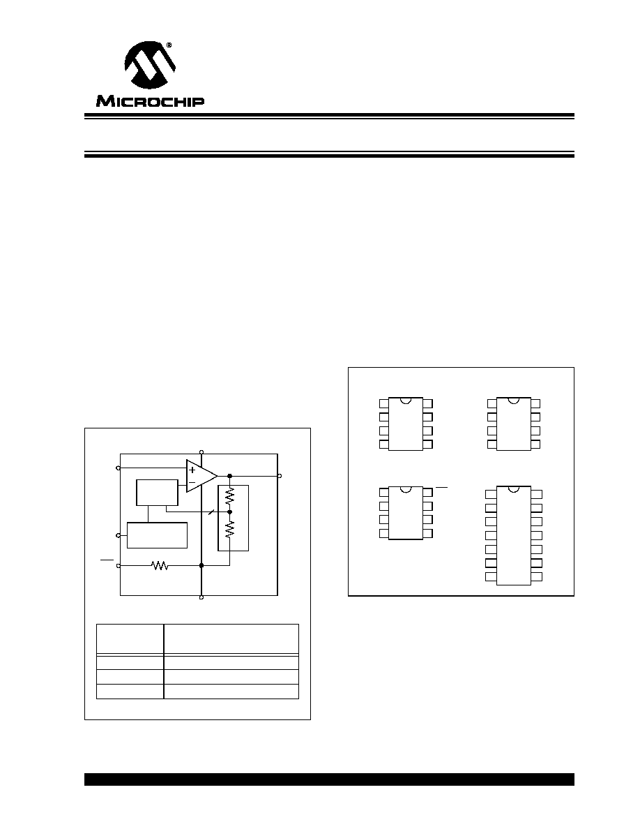
Block Diagram
Description
The Microchip Technology Inc. MCP6G01/2/3/4 are
analog Selectable Gain Amplifiers (SGA). They can be
configured for gains of +1 V/V, +10 V/V, and +50 V/V
through the Gain Select input pin(s). The Chip Select
pin on the MCP6G03 can put it into shutdown to
conserve power. These SGAs are optimized for single
supply applications requiring reasonable quiescent
current and speed.
The single amplifier MCP6G01 and MCP6G03, and the
dual amplifier MCP6G02, are available in 8-pin SOIC
and MSOP packages. The quad amplifier MCP6G04 is
available in 14-pin SOIC and TSSOP packages. All
parts are fully specified from -40°C to +125°C.
Package Types
V
OUT
V
DD
GSEL
V
IN
V
SS
3
R
F
R
G
Gain Select
Logic
Gain
Switches
Resistor Lad
der
(R
LA
D
)
Gain
(V/V)
GSEL Voltage (Typ.)
(V)
1
V
DD
/2 (or open)
10
0
50
V
DD
Note:
V
SS
is assumed to be 0V
CS
(MCP6G03
only)
5 M
V
IN
GSEL
V
SS
V
OUT
V
DD
1
2
3
4
8
7
6
5
NC
NC
NC
GSEL
A
V
OUTA
V
INA
GSEL
C
V
INC
1
2
3
4
14
13
12
11 V
SS
V
OUTC
GSEL
D
5
6
7
10
9
8
V
DD
GSEL
B
V
OUTD
V
OUTB
V
IND
V
INB
MCP6G01
SOIC, MSOP
V
INA
GSEL
A
V
SS
GSEL
B
V
OUTB
1
2
3
4
8
7
6
5
V
DD
V
INB
V
OUTA
MCP6G02
SOIC, MSOP
MCP6G04
SOIC, TSSOP
V
IN
GSEL
V
SS
V
OUT
V
DD
1
2
3
4
8
7
6
5
CS
NC
NC
MCP6G03
SOIC, MSOP
110 µA Selectable Gain Amplifier
MCP6G01/2/3/4
DS22004A-page 2
© 2006 Microchip Technology Inc.
1.0
ELECTRICAL
CHARACTERISTICS
Absolute Maximum Ratings
V
DD
V
SS
........................................................................7.0V
Current at Analog Input Pin (V
IN
)
......................................±2 mA
Analog Input (V
IN
) ..................... V
SS
1.0V to V
DD
+ 1.0V
All other Inputs and Outputs........... V
SS
0.3V to V
DD
+ 0.3V
Output Short Circuit Current...................................continuous
Current at Output and Supply Pins
................................ ±30 mA
Storage Temperature.....................................-65°C to +150°C
Junction Temperature..................................................+150°C
ESD protection on all pins (HBM; MM)
................ 4 kV; 200V
Notice: Stresses above those listed under "Absolute
Maximum Ratings" may cause permanent damage to the
device. This is a stress rating only and functional operation of
the device at those or any other conditions above those
indicated in the operational listings of this specification is not
implied. Exposure to maximum rating conditions for extended
periods may affect device reliability.
See Section 4.1.4 "Input Voltage and Current Limits".
DC ELECTRICAL CHARACTERISTICS
Electrical Specifications: Unless otherwise indicated, T
A
= +25°C, V
DD
= +1.8V to +5.5V, V
SS
= GND, G = +1 V/V,
V
IN
= (0.3V)/G, R
L
= 100 k
to V
DD
/2, GSEL = V
DD
/2, and CS is tied low.
Parameters
Sym
Min
Typ
Max
Units
Conditions
Amplifier Inputs (V
IN
)
Input Offset Voltage
V
OS
4.5
±1.0
+4.5
mV
G = +1
--
±1.0
--
mV
G = +10, +50
Input Offset Voltage Drift
V
OS
/
T
A
--
±2
--
µV/°C
G = +1, T
A
= -40°C to +125°C
Power Supply Rejection Ratio
PSRR
65
80
--
dB
G = +1 (Note 1)
Input Bias Current
I
B
--
1
--
pA
Input Bias Current at
I
B
--
30
--
pA
T
A
= +85°C
Temperature
I
B
--
1000
5000
pA
T
A
= +125°C
Input Impedance
Z
IN
--
10
13
||6
--
||pF
Amplifier Gain
Nominal Gains
G
--
1 to 50
--
V/V
+1, +10 or +50
DC Gain Error G = +1
g
E
0.3
--
+0.3
%
V
OUT
0.3V to V
DD
- 0.3V
G
+10
g
E
1.0
--
+1.0
%
V
OUT
0.3V to V
DD
- 0.3V
DC Gain Drift G = +1
G/T
A
--
±1
--
ppm/°C
T
A
= -40°C to +125°C
G
+10
G/T
A
--
±4
--
ppm/°C
T
A
= -40°C to +1285°C
Ladder Resistance (Note 1)
Ladder Resistance
R
LAD
200
350
500
k
Ladder Resistance
across Temperature
R
LAD
/
T
A
--
1800
--
ppm/°C
T
A
= -40°C to +125°C
Amplifier Output
DC Output Non-linearity G = +1
V
ONL
0.2
--
+0.2
% of FSR V
OUT
= 0.3V to V
DD
0.3V,
V
DD
= 1.8V
V
ONL
0.1
--
+0.1
% of FSR V
OUT
= 0.3V to V
DD
0.3V,
V
DD
= 5.5V
DC Output Non-linearity, G = +10, +50
V
ONL
0.05
--
+0.05
% of FSR V
OUT
= 0.3V to V
DD
0.3V
Maximum Output Voltage Swing
V
OH
, V
OL
V
SS
+10
--
V
DD
10
mV
G = +1; 0.3V output overdrive
V
OH
, V
OL
V
SS
+10
--
V
DD
10
mV
G
+10; 0.5V output overdrive
Short Circuit Current
I
SC
--
±7
--
mA
V
DD
= 1.8V
I
SC
--
±20
--
mA
V
DD
= 5.5V
Note 1:
R
LAD
(R
F
+R
G
in
Figure 4-1
) connects V
SS
, V
OUT
, and the inverting input of the internal amplifier. Thus, V
SS
is coupled
to the internal amplifier and the PSRR spec describes PSRR+ only. It is recommended that the V
SS
pin be tied directly
to ground to avoid noise problems.
2:
I
Q
includes current in R
LAD
(typically 0.6 µA at V
OUT
= 0.3V), and excludes digital switching currents.
© 2006 Microchip Technology Inc.
DS22004A-page 3
MCP6G01/2/3/4
Power Supply
Supply Voltage
V
DD
1.8
--
5.5
V
Quiescent Current per Amplifier
I
Q
60
110
170
µA
I
O
= 0 (Note 2)
DC ELECTRICAL CHARACTERISTICS (CONTINUED)
Electrical Specifications: Unless otherwise indicated, T
A
= +25°C, V
DD
= +1.8V to +5.5V, V
SS
= GND, G = +1 V/V,
V
IN
= (0.3V)/G, R
L
= 100 k
to V
DD
/2, GSEL = V
DD
/2, and CS is tied low.
Parameters
Sym
Min
Typ
Max
Units
Conditions
Note 1:
R
LAD
(R
F
+R
G
in
Figure 4-1
) connects V
SS
, V
OUT
, and the inverting input of the internal amplifier. Thus, V
SS
is coupled
to the internal amplifier and the PSRR spec describes PSRR+ only. It is recommended that the V
SS
pin be tied directly
to ground to avoid noise problems.
2:
I
Q
includes current in R
LAD
(typically 0.6 µA at V
OUT
= 0.3V), and excludes digital switching currents.
AC ELECTRICAL CHARACTERISTICS
Electrical Specifications: Unless otherwise indicated, T
A
= +25°C, V
DD
= +1.8V to +5.5V, V
SS
= GND, G = +1 V/V,
V
IN
= (0.3V)/G, R
L
= 100 k
to V
DD
/2, C
L
= 60 pF, GSEL = V
DD
/2, and CS is tied low.
Parameters
Sym
Min
Typ
Max
Units
Conditions
Frequency Response
-3dB Bandwidth
BW
--
900
--
kHz
G = +1, V
OUT
< 100 mV
P-P
(Note 1)
BW
--
350
--
kHz
G = +10, V
OUT
< 100 mV
P-P
(Note 1)
BW
--
250
--
kHz
G = +50, V
OUT
< 100 mV
P-P
(Note 1)
Gain Peaking
GPK
--
0.3
--
dB
G = +1; V
OUT
< 100 mV
P-P
GPK
--
0
--
dB
G = +10, V
OUT
< 100 mV
P-P
GPK
--
0.7
--
dB
G = +50; V
OUT
< 100 mV
P-P
Total Harmonic Distortion plus Noise
f = 1 kHz, G = +1 V/V
THD+N
--
0.0029
--
%
V
OUT
= 1.75V ± 1.4V
PK
, V
DD
= 5.0V,
BW = 80 kHz
f = 1 kHz, G = +10 V/V
THD+N
--
0.18
--
%
V
OUT
= 2.5V ± 1.4V
PK
, V
DD
= 5.0V,
BW = 80 kHz
f = 1 kHz, G = +50 V/V
THD+N
--
1.3
--
%
V
OUT
= 2.5V ± 1.4V
PK
, V
DD
= 5.0V,
BW = 80 kHz
Step Response
Slew Rate
SR
--
0.50
--
V/µs
G = 1
SR
--
2.3
--
V/µs
G = 10
SR
--
4.5
--
V/µs
G = 50
Noise
Input Noise Voltage
E
ni
--
9
--
µV
P-P
f = 0.1 Hz to 10 Hz (Note 2)
E
ni
--
50
--
µV
P-P
f = 0.1 Hz to 30 kHz (Note 2)
Input Noise Voltage Density
e
ni
--
38
--
nV/
Hz G = +1 V/V, f = 10 kHz (Note 2)
e
ni
--
46
--
nV/
Hz G = +10 V/V, f = 10 kHz (Note 2)
e
ni
--
41
--
nV/
Hz G = +50 V/V, f = 10 kHz (Note 2)
Input Noise Current Density
i
ni
--
4
--
fA/
Hz f = 10 kHz
Note 1:
See
Table 4-1
for a list of typical numbers and
Figure 2-31
for the frequency response versus gain.
2:
E
ni
and e
ni
include ladder resistance thermal noise.
MCP6G01/2/3/4
DS22004A-page 4
© 2006 Microchip Technology Inc.
DIGITAL ELECTRICAL CHARACTERISTICS
Electrical Specifications: Unless otherwise indicated, T
A
= 25°C, V
DD
= +1.8V to +5.5V, V
SS
= GND, G = +1 V/V, V
IN
= (0.3V)/G,
R
L
= 100 k
to V
DD
/2, C
L
= 60 pF, GSEL = V
DD
/2, and CS is tied low.
Parameters
Sym
Min
Typ
Max
Units
Conditions
CS Low Specifications
CS Logic Threshold, Low
V
CSL
0
--
0.2V
DD
V
CS = 0V
CS Input Current, Low
I
CSL
--
30
--
pA
CS = 0V
CS High Specifications
CS Logic Threshold, High
V
CSH
0.8V
DD
--
V
DD
V
CS = V
DD
CS Input Current, High
I
CSH
--
0.8
--
µA
CS = V
DD
= 5.5V
Quiescent Current per Amplifier,
Shutdown Mode (I
DD
)
I
DD_SHDN
--
120
--
pA
CS = V
DD
, MCP6G03
Quiescent Current per Amplifier,
Shutdown Mode (I
SS
) (Note 3)
I
SS_SHDN
--
2.4
--
µA
CS = V
DD
= 1.8V, MCP6G03
I
SS_SHDN
--
7.2
--
µA
CS = V
DD
= 5.5V, MCP6G03
CS Dynamic Specifications
Input Capacitance
C
CS
--
10
--
pF
Input Rise/Fall Times
t
CSRF
--
--
2
µs
(Note 2)
CS Low to Amplifier Output High
Turn-on Time
t
CSON
--
40
--
µs
G = +1 V/V, V
DD
= 1.8V, V
IN
= 0.9V
DD
CS = 0.2V
DD
to V
OUT
= 0.8V
DD
t
CSON
--
7
--
µs
G = +1 V/V, V
DD
= 5.5V, V
IN
= 0.9V
DD
CS = 0.2V
DD
to V
OUT
= 0.8V
DD
CS High to Amplifier Output High-Z
Turn-off Time
t
CSOFF
--
30
--
µs
G = +1 V/V, V
IN
= V
DD
/2,
CS = 0.8V
DD
to V
OUT
= 0.1V
DD
/2
Hysteresis
V
CSHY
--
0.40
--
V
V
DD
= 1.8V
V
CSHY
--
0.55
--
V
V
DD
= 5.5V
GSEL Specifications (Note 1)
GSEL Logic Threshold, Low
V
GSL
0.15V
DD
--
0.35V
DD
V
Gain changes between 1 and 10,
I
GSEL
= 0
GSEL Logic Threshold, High
V
GSH
0.65V
DD
--
0.85V
DD
V
Gain changes between 1 and 50,
I
GSEL
= 0
GSEL Input Current, Low
I
GSL
10
--
1.5
µA
GSEL voltage = 0.3V
DD
GSEL Input Current, High
I
GSH
+1.5
--
+10
µA
GSEL voltage = 0.7V
DD
GSEL Dynamic Specifications (Note 1)
Input Capacitance
C
GSEL
--
8
--
pF
Input Rise/Fall Times
t
GSRF
--
--
10
µs
(Note 2)
Hysteresis
V
GSHY
--
45
--
mV
V
DD
= 1.8V
V
GSHY
--
95
--
mV
V
DD
= 5.5V
GSEL Low to Valid Output Time,
G = +1 to +10 Select
t
GSL1
--
10
--
µs
V
IN
= 150 mV,
GSEL = 0.25V
DD
to V
OUT
= 1.37V
GSEL Middle to Valid Output Time,
G = +10 to +1 Select
t
GSM10
--
12
--
µs
V
IN
= 150 mV,
GSEL = 0.25V
DD
to V
OUT
= 0.28V
GSEL High to Valid Output Time,
G = +1 to +50 Select
t
GSH1
--
9
--
µs
V
IN
= 30 mV,
GSEL = 0.75V
DD
to V
OUT
= 1.35V
GSEL Middle to Valid Output Time,
G = +50 to +1 Select
t
GSM50
--
8
--
µs
V
IN
= 30 mV,
GSEL = 0.75V
DD
to V
OUT
= 0.18V
Note 1:
GSEL is a tri-level input pin. The gain is 10 when its voltage is low, 1 when it is at mid-suppy, and 50 when it is high.
2:
Not tested in production. Set by design and characterization.
3:
I
SS_SHDN
includes the current through the CS pin, R
L
and R
LAD
, and excludes digital switching currents. The block dia-
gram on the from page shows these current paths (through V
SS
).
© 2006 Microchip Technology Inc.
DS22004A-page 5
MCP6G01/2/3/4
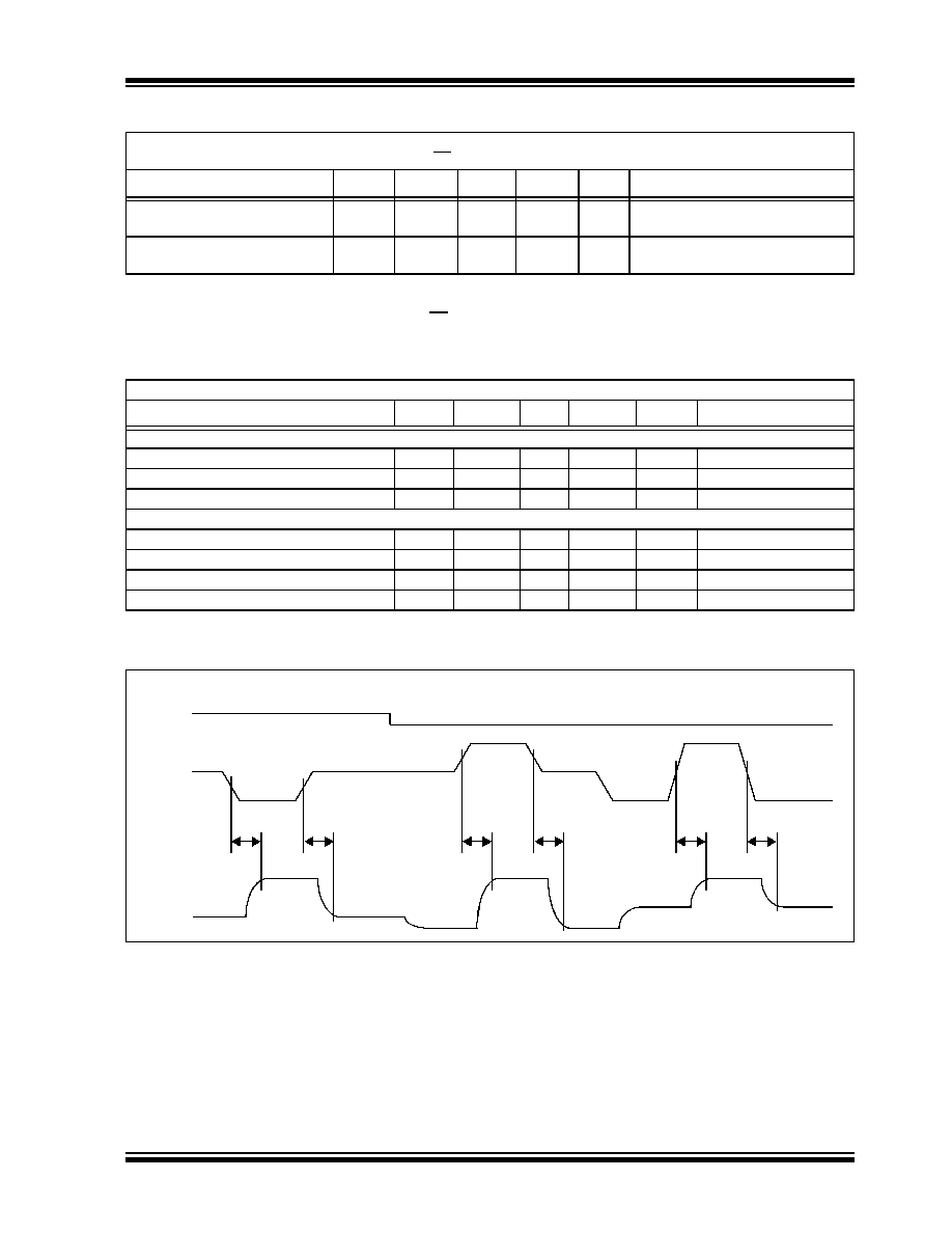
FIGURE 1-1:
Gain Select Timing Diagram.
GSEL High to Valid Output Time,
G = +10 to +50 Select
t
GSH10
--
12
--
µs
V
IN
= 30 mV,
GSEL = 0.75V
DD
to V
OUT
= 1.38V
GSEL Low to Valid Output Time,
G = +50 to +10 Select
t
GSL50
--
9
--
µs
V
IN
= 30 mV,
GSEL = 0.25V
DD
to V
OUT
= 0.42V
DIGITAL ELECTRICAL CHARACTERISTICS (CONTINUED)
Electrical Specifications: Unless otherwise indicated, T
A
= 25°C, V
DD
= +1.8V to +5.5V, V
SS
= GND, G = +1 V/V, V
IN
= (0.3V)/G,
R
L
= 100 k
to V
DD
/2, C
L
= 60 pF, GSEL = V
DD
/2, and CS is tied low.
Parameters
Sym
Min
Typ
Max
Units
Conditions
Note 1:
GSEL is a tri-level input pin. The gain is 10 when its voltage is low, 1 when it is at mid-suppy, and 50 when it is high.
2:
Not tested in production. Set by design and characterization.
3:
I
SS_SHDN
includes the current through the CS pin, R
L
and R
LAD
, and excludes digital switching currents. The block dia-
gram on the from page shows these current paths (through V
SS
).
TEMPERATURE CHARACTERISTICS
Electrical Specifications: Unless otherwise indicated, V
DD
= +1.8V to +5.5V, and V
SS
= GND.
Parameters
Sym
Min
Typ
Max
Units
Conditions
Temperature Ranges
Specified Temperature Range
T
A
40
--
+125
°C
Operating Temperature Range
T
A
40
--
+125
°C
(Note 1)
Storage Temperature Range
T
A
65
--
+150
°C
Thermal Package Resistances
Thermal Resistance, 8L-SOIC
JA
--
163
--
°C/W
Thermal Resistance, 8L-MSOP
JA
--
206
--
°C/W
Thermal Resistance, 14L-SOIC
JA
--
120
--
°C/W
Thermal Resistance, 14L-TSSOP
JA
--
100
--
°C/W
Note 1:
The MCP6G01/2/3/4 family of SGAs operates over this temperature range, but operation must not cause T
J
to exceed
Maximum Junction Temperature (+150°C).
GSEL
V
OUT
t
GSL1
0.15V
1.50V
V
IN
0.150V
0.030V
0.15V
t
GSM10
0.03V
1.50V
t
GSH1
0.03V
t
GSM50
0.30V
1.50V
t
GSH10
0.30V
t
GSL50
MCP6G01/2/3/4
DS22004A-page 6
© 2006 Microchip Technology Inc.
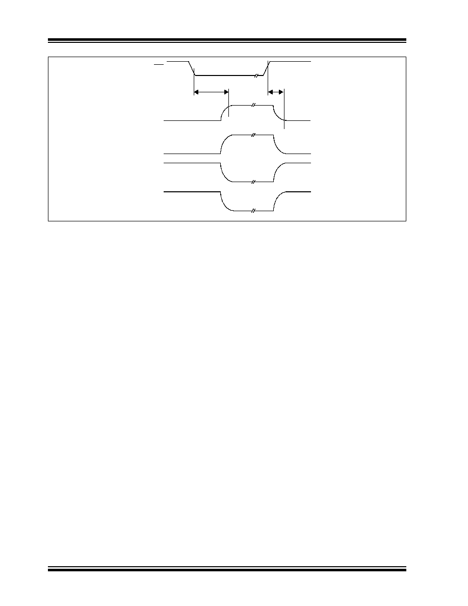
FIGURE 1-2:
SGA Chip Select Timing Diagram.
CS
t
CSOFF
V
OUT
t
CSON
High-Z
High-Z
I
DD
120 pA (typ.)
110 µA (typ.)
0.9V
DD
I
SS
V
DD
/ 7 M
(typ.)
110 µA (typ.)
I
CS
30 pA (typ.)
V
DD
/ 7 M
(typ.)
© 2006 Microchip Technology Inc.
DS22004A-page 7
MCP6G01/2/3/4
1.1
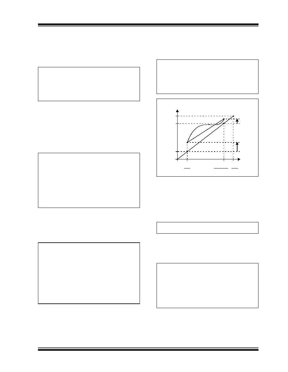
DC Output Voltage Specs / Model
1.1.1
IDEAL MODEL
The ideal SGA output voltage (V
OUT
) is (see
Figure 1-3
):
EQUATION 1-1:
This equation holds when there are no gain or offset
errors.
1.1.2
LINEAR MODEL
The SGA's linear region of operation is modeled by the
line V
O_LIN
shown in
Figure 1-3
. V
O_LIN
includes offset
and gain errors, but does not include non-linear effects.
EQUATION 1-2:
This line's endpoints are 0.3V from the supply rails
(V
O_ID
= 0.3V and V
DD
0.3V). The gain error and
input offset voltage specifications (in the electrical
specifications) relate to
Figure 1-3
as follows:
EQUATION 1-3:
The input offset specification describes V
OS
at
G = +1 V/V.
The DC Gain Drift (
G/T
A
) can be calculated from the
change in g
E
across temperature. This is shown in the
following equation:
EQUATION 1-4:
FIGURE 1-3:
Output Voltage Model.
1.1.3
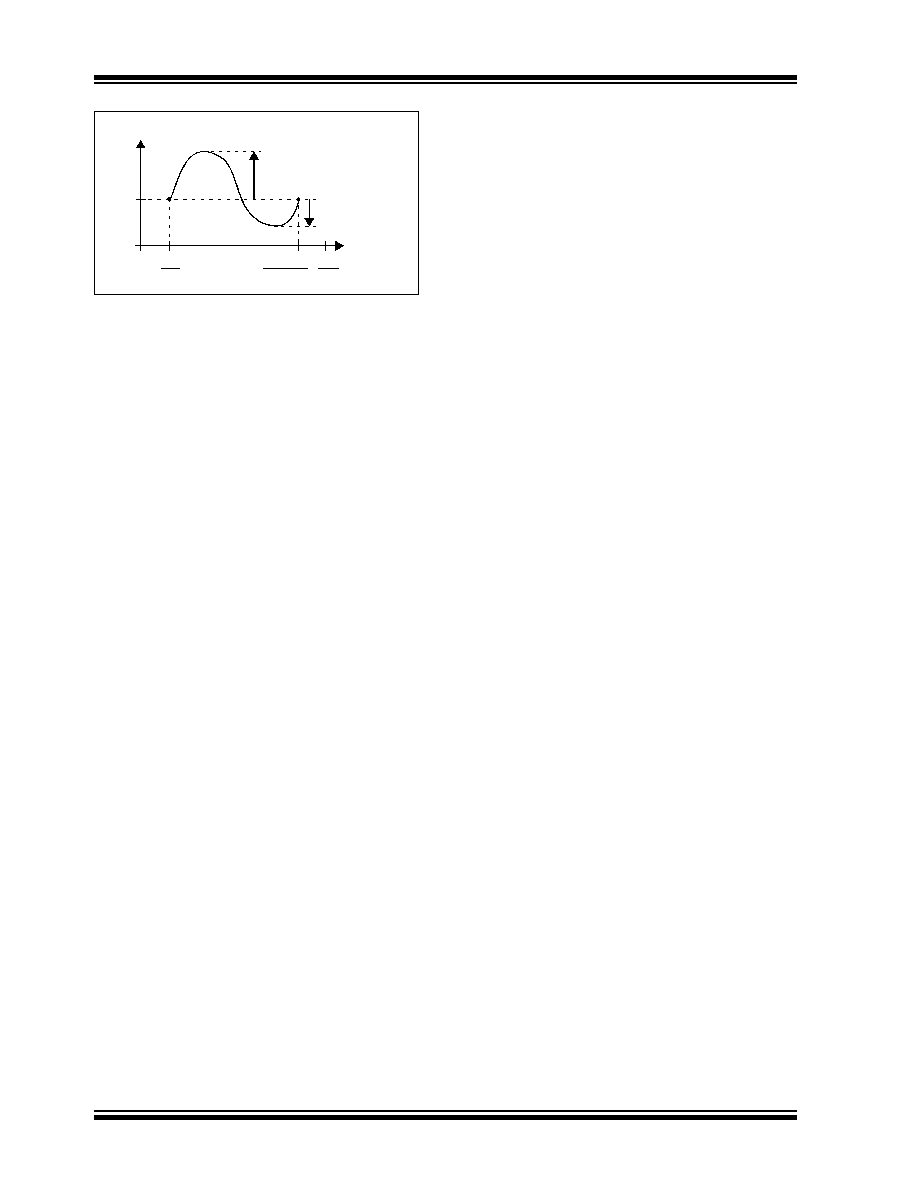
OUTPUT NON-LINEARITY
Figure 1-4
shows the Integral Non-Linearity (INL) of the
output voltage. INL is the output non-linearity error not
explained by V
O_LIN
:
EQUATION 1-5:
The output non-linearity specification (in the Electrical
Specifications, with units of % of FSR) is related to
Figure 1-4
by:
EQUATION 1-6:
Note that the Full Scale Range (FSR) is V
DD
0.6V
(0.3V to V
DD
0.3V).
Where:
G is the nominal gain
V
O_ID
GV
IN
=
V
REF
V
SS
0V
=
=
V
O_LIN
G 1 g
E
+
(
) V
IN
0.3V
G
------------ V
OS
+
0.3V
+
=
V
REF
V
SS
0V
=
=
Where:
G is the nominal gain
g
E
is the gain error
V
OS
is the input offset voltage
g
E
100%
V
2
V
1
V
DD
0.6V
-----------------------------
=
V
OS
V
1
G 1 g
E
+
(
)
-------------------------,
=
G
+1
=
Where:
V
1
V
OUT
V
O_ID
,
=
V
O_ID
0.3V
=
V
2
V
OUT
V
O_ID
,
=
V
O_ID
V
DD
0.3V
=
G
T
A
/
G
g
E
T
A
----------,
=
in units of V/V/°C
G
T
A
/
100%
g
E
T
A
----------,
=
in units of %/°C
0
0
0.3
V
DD
-0.3
V
DD
V
OUT
V
OUT
(V)
V
IN
(V)
0.3
V
DD
-0.3 V
DD
G
G
G
V
1
V
O_
ID
V
O_
LIN
V
2
INL
V
OUT
V
O_LIN
=
V
ONL
100%
max V
3
V
4
,
(
)
V
DD
0.6V
-------------------------------
=
V
3
max INL
(
)
=
Where:
V
4
max INL
(
)
=
MCP6G01/2/3/4
DS22004A-page 8
© 2006 Microchip Technology Inc.
FIGURE 1-4:
Output Voltage INL.
0
INL (V)
V
IN
(V)
0.3
V
DD
-0.3 V
DD
G
G
G
0
V
3
V
4
© 2006 Microchip Technology Inc.
DS22004A-page 9
MCP6G01/2/3/4
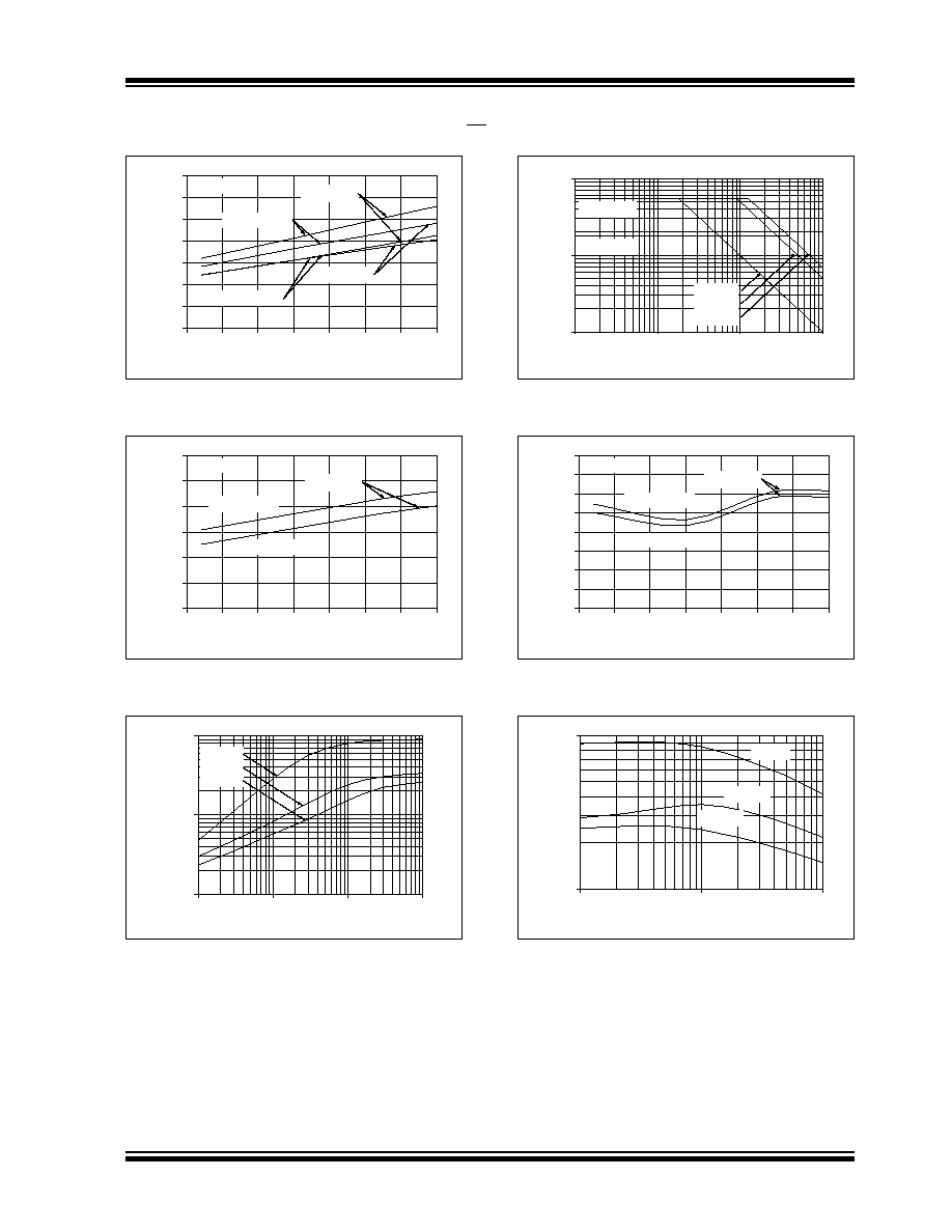
2.0
TYPICAL PERFORMANCE CURVES
Note: Unless otherwise indicated, T
A
= +25°C, V
DD
= +1.8V to +5.5V, V
SS
= GND, G = +1 V/V, V
IN
= (0.3V)/G,
R
L
= 100 k
to V
DD
/2, C
L
= 60 pF, GSEL = V
DD
/2, and CS is tied low.
FIGURE 2-1:
DC Gain Error, G = +1.
FIGURE 2-2:
DC Gain Error, G
+10.
FIGURE 2-3:
Input Offset Voltage.
FIGURE 2-4:
DC Gain Drift, G = +1.
FIGURE 2-5:
DC Gain Drift, G
+10.
FIGURE 2-6:
Input Offset Voltage Drift.
Note:
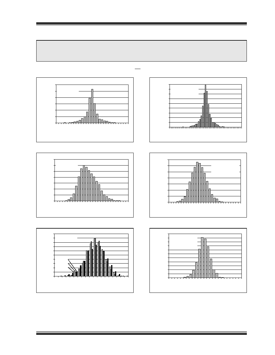
The graphs and tables provided following this note are a statistical summary based on a limited number of
samples and are provided for informational purposes only. The performance characteristics listed herein
are not tested or guaranteed. In some graphs or tables, the data presented may be outside the specified
operating range (e.g., outside specified power supply range) and therefore outside the warranted range.
0%
5%
10%
15%
20%
25%
30%
-0
.2
8
-0
.2
4
-0
.2
0
-0
.1
6
-0
.1
2
-0
.0
8
-0
.0
4
0.0
0
0.0
4
0.0
8
0.1
2
0.1
6
0.2
0
0.2
4
0.2
8
DC Gain Error (%)
Per
cen
t
a
g
e
of
Occ
u
r
r
en
ces
2460 Samples
G = +1
0%
2%
4%
6%
8%
10%
12%
14%
-0
.7
-0
.6
-0
.5
-0
.4
-0
.3
-0
.2
-0
.1
0.
0
0.
1
0.
2
0.
3
0.
4
0.
5
0.
6
0.
7
DC Gain Error (%)
Per
cen
t
a
g
e
of
Occ
u
r
r
en
ces
4916 Samples
G +10
0%
2%
4%
6%
8%
10%
12%
14%
16%
18%
20%
-4
.5
-3
.5
-2
.5
-1
.5
-0
.5
0.
5
1.
5
2.
5
3.
5
4.
5
Input Offset Voltage (mV)
P
e
rce
n
ta
ge
o
f
O
ccu
rr
en
ces
2460 Samples
G = +50
G = +10
G = +1
0%
2%
4%
6%
8%
10%
12%
14%
16%
18%
-5
-4
-3
-2
-1
0
1
2
3
4
5
DC Gain Drift (ppm/°C)
Perce
n
ta
g
e
of Oc
curre
n
c
es
2459 Samples
G = +1
T
A
= -40 to +125°C
0%
2%
4%
6%
8%
10%
12%
14%
-1
4
-1
2
-1
0
-8
-6
-4
-2
0
2
4
6
8
10
12
14
DC Gain Drift (ppm/°C)
Perce
n
ta
g
e
of Oc
curre
n
c
es
4912 Samples
G +10
T
A
= -40 to +125°C
0%
2%
4%
6%
8%
10%
12%
14%
16%
18%
20%
22%
-1
2
-1
0
-8
-6
-4
-2
0
2
4
6
8
10
12
Input Offset Voltage Drift (µV/°C)
Per
cen
t
a
g
e
of
Oc
cu
rren
c
e
s
1612 Samples
G = +1, +10, +50
T
A
= -40 to +125°C
MCP6G01/2/3/4
DS22004A-page 10
© 2006 Microchip Technology Inc.
Note: Unless otherwise indicated, T
A
= +25°C, V
DD
= +1.8V to +5.5V, V
SS
= GND, G = +1 V/V, V
IN
= (0.3V)/G,
R
L
= 100 k
to V
DD
/2, C
L
= 60 pF, GSEL = V
DD
/2, and CS is tied low.
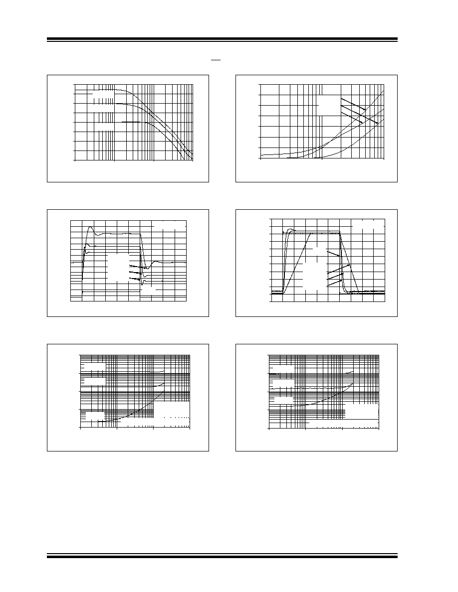
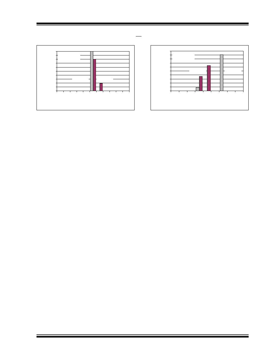
FIGURE 2-7:
The MCP6G01/2/3/4 family
shows no phase reversal under overdrive.
FIGURE 2-8:
PSRR vs. Temperature.
FIGURE 2-9:
Input Noise Voltage Density
vs. Frequency.
FIGURE 2-10:
Crosstalk vs. Frequency,
with G = 50 (circuit in
Figure 4-7
).
FIGURE 2-11:
PSRR vs. Frequency.
FIGURE 2-12:
Quiescent Current vs.
Supply Voltage.
-1
0
1
2
3
4
5
6
0.0E+00
1.0E-03
2.0E-03
3.0E-03
4.0E-03
5.0E-03
6.0E-03
7.0E-03
8.0E-03
9.0E-03
1.0E-02
Time (1 ms/div)
Inpu
t,
O
u
tput
Volta
g
e (V)
V
DD
= 5.0V
G = +1 V/V
V
IN
V
OUT
70
80
90
100
110
120
-50
-25
0
25
50
75
100
125
Ambient Temperature (°C)
PSRR
(
d
B)
10
100
1000
10000
0.1
1
10
100
1000 10000 10000
0
Frequency (Hz)
Input Noise Voltage Density
(nV/
Hz)
1k
10k
100k
1
10
100
0.1
G = +1
= +10
= +50
-120
-110
-100
-90
-80
-70
-60
-50
-40
-30
-20
-10
0
1.E+03
1.E+04
1.E+05
Frequency (Hz)
C
r
os
sta
l
k, Inpu
t R
e
ferre
d
(d
B)
1k
100k
10k
V
DD
= 5.0V
G = 50 V/V
R
S
= 0
R
S
= 1 M
R
S
= 100 k
R
S
= 10 k
20
30
40
50
60
70
80
90
100
1000
10000
100000
Frequency (Hz)
Po
w
e
r Sup
p
ly
Reje
ct
ion
Rat
i
o
(dB
)
Input Referred
G = 1
G = 10
G = 50
V
DD
= 1.8V
V
DD
= 5.5V
100
1k
10k
100k
0
20
40
60
80
100
120
140
160
0.0 0.5 1.0 1.5 2.0 2.5 3.0 3.5 4.0 4.5 5.0 5.5
Power Supply Voltage (V)
Qu
ie
scen
t
C
u
rren
t
(
m
A
)
T
A
= +25°C
T
A
= 40°C
T
A
= +125°C
T
A
= +85°C
© 2006 Microchip Technology Inc.
DS22004A-page 11
MCP6G01/2/3/4
Note: Unless otherwise indicated, T
A
= +25°C, V
DD
= +1.8V to +5.5V, V
SS
= GND, G = +1 V/V, V
IN
= (0.3V)/G,
R
L
= 100 k
to V
DD
/2, C
L
= 60 pF, GSEL = V
DD
/2, and CS is tied low.
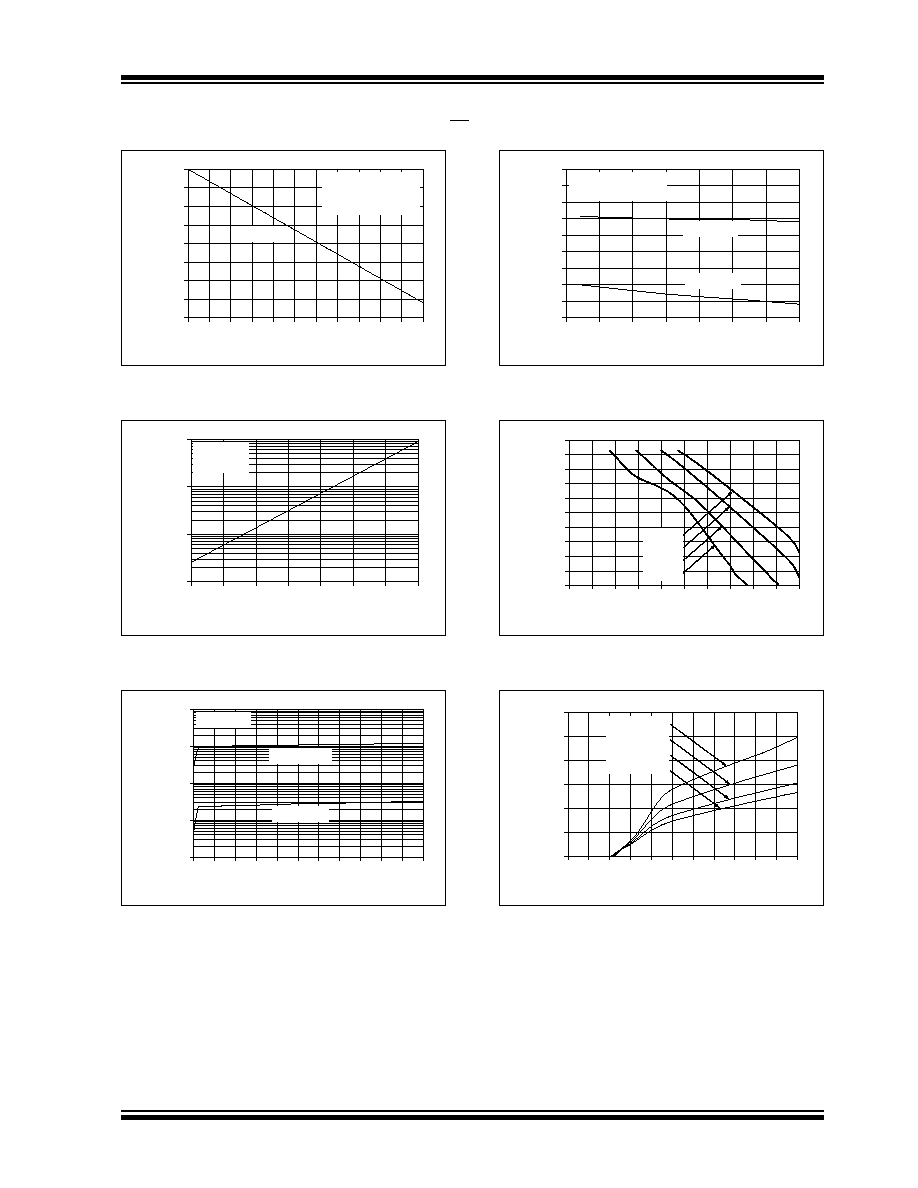
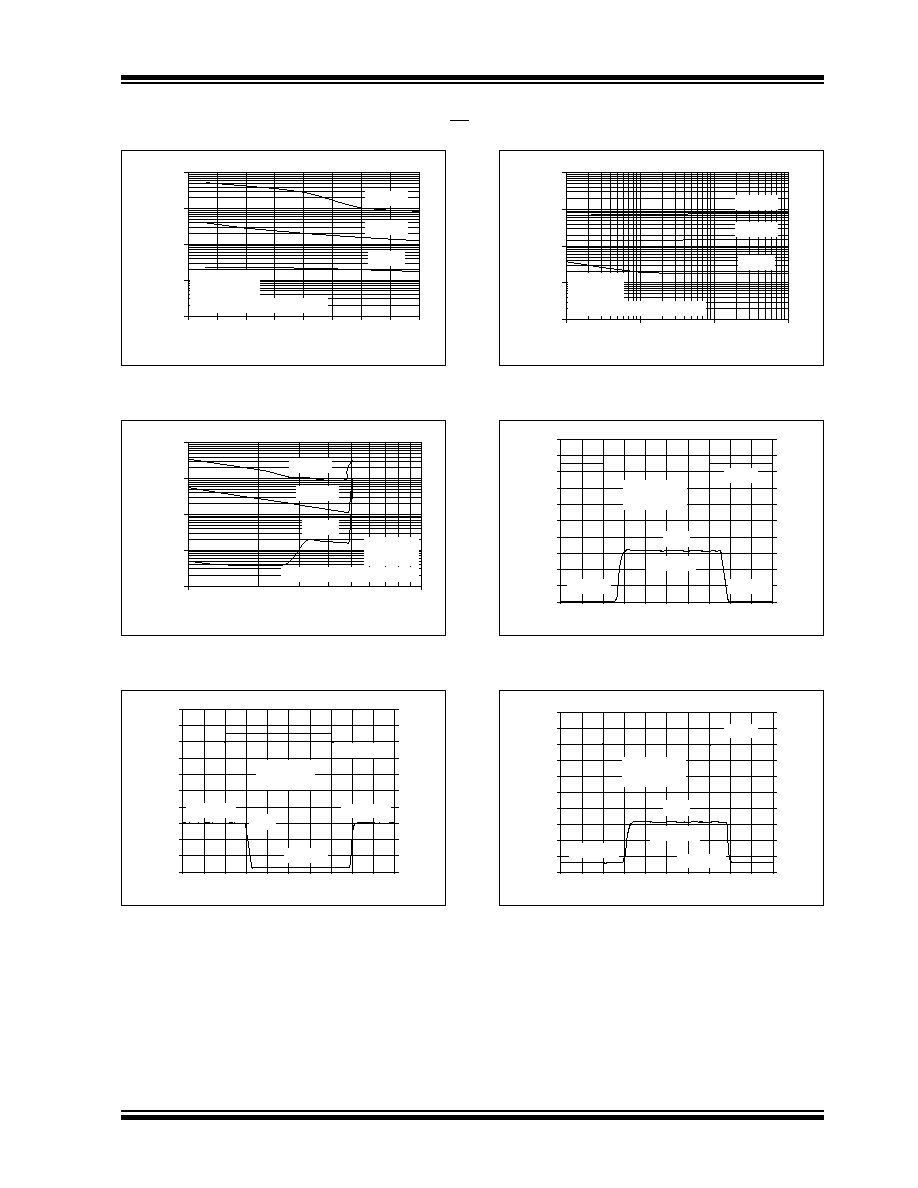
FIGURE 2-13:
Quiescent Current (I
SS
) in
Shutdown Mode vs. Supply Voltage.
FIGURE 2-14:
Input Bias Current vs.
Temperature.
FIGURE 2-15:
Input Bias Current vs. Input
Voltage.
FIGURE 2-16:
Quiescent Current (I
SS
) in
Shutdown Mode vs. Temperature.
FIGURE 2-17:
Input Bias Current vs. Input
Voltage.
FIGURE 2-18:
Output Short Circuit Current
vs. Supply Voltage.
-8
-7
-6
-5
-4
-3
-2
-1
0
0.0 0.5 1.0 1.5 2.0 2.5 3.0 3.5 4.0 4.5 5.0 5.5
Power Supply Voltage (V)
Qu
i
esc
en
t
C
u
r
r
en
t
i
n
Sh
utdo
w
n
(µA
)
In Shutdown Mode
V
IN
= V
DD
/2
CS = V
DD
I
SS_SHDN
1
10
100
1,000
55
65
75
85
95
105
115
125
Ambient Temperature (°C)
In
p
u
t
Bi
as Cu
r
r
e
nt
(p
A)
V
DD
= 5.5V
V
IN
= V
DD
1
10
100
1,000
10,000
0.0 0.5 1.0 1.5 2.0 2.5 3.0 3.5 4.0 4.5 5.0 5.5
Input Voltage (V)
Input
B
i
a
s
Cu
rr
e
n
t (pA
)
T
A
= +85°C
V
DD
= 5.5V
T
A
= +125°C
-9
-8
-7
-6
-5
-4
-3
-2
-1
0
-50
-25
0
25
50
75
100
125
Ambient Temperature (°C)
Qu
i
esc
en
t
C
u
r
r
en
t
i
n
Sh
utdo
w
n
(µA
)
In Shutdown Mode
V
IN
= V
DD
/2
V
DD
= 5.5V
V
DD
= 1.8V
1.E-12
1.E-11
1.E-10
1.E-09
1.E-08
1.E-07
1.E-06
1.E-05
1.E-04
1.E-03
1.E-02
-1.0 -0.9 -0.8 -0.7 -0.6 -0.5 -0.4 -0.3 -0.2 -0.1 0.0
Input Voltage (V)
I
n
put
C
u
rr
e
n
t
Ma
gn
i
t
u
d
e
(A
)
+125°C
+85°C
+25°C
-40°C
10m
1m
100µ
10µ
1µ
100n
10n
1n
100p
10p
1p
0
5
10
15
20
25
30
0.0 0.5 1.0 1.5 2.0 2.5 3.0 3.5 4.0 4.5 5.0 5.5
Power Supply Voltage (V)
Outp
ut S
hort Ci
rcu
i
t Cu
rre
n
t
Ma
gnitude
(mA)
T
A
= 40°C
T
A
= +25°C
T
A
= +85°C
T
A
= +125°C
MCP6G01/2/3/4
DS22004A-page 12
© 2006 Microchip Technology Inc.
Note: Unless otherwise indicated, T
A
= +25°C, V
DD
= +1.8V to +5.5V, V
SS
= GND, G = +1 V/V, V
IN
= (0.3V)/G,
R
L
= 100 k
to V
DD
/2, C
L
= 60 pF, GSEL = V
DD
/2, and CS is tied low.
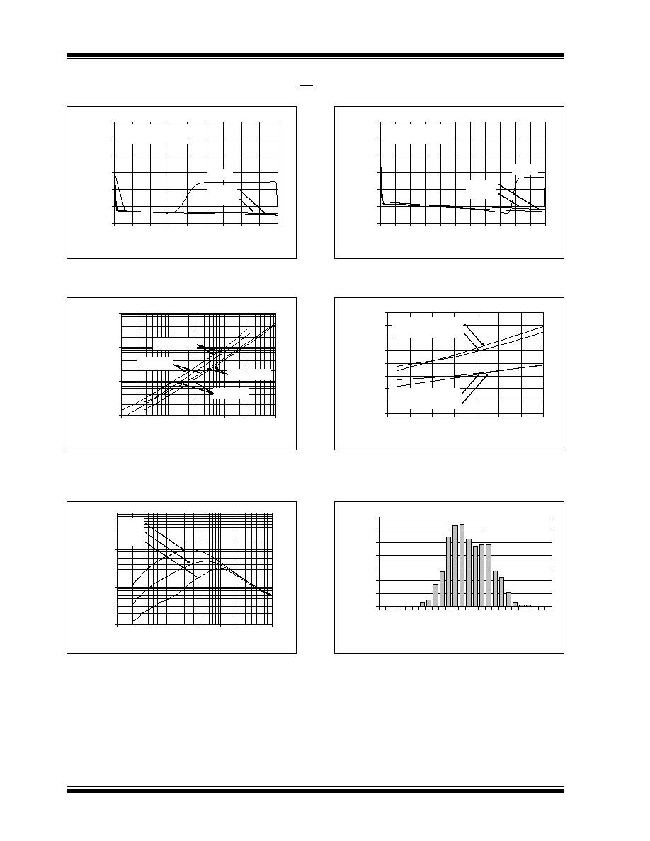
FIGURE 2-19:
Output Voltage Error vs.
Ideal Output Voltage, with V
DD
= 1.8V.
FIGURE 2-20:
Output Voltage Headroom
vs. Output plus Ladder Current (circuit in
Figure 4-4
).
FIGURE 2-21:
Output Impedance vs.
Frequency.
FIGURE 2-22:
Output Voltage Error vs.
Ideal Output Voltage, with V
DD
= 5.5V.
FIGURE 2-23:
Output Voltage Headroom
vs. Temperature.
FIGURE 2-24:
Ladder Resistance Drift.
-3
-2
-1
0
1
2
3
0.0 0.2 0.4 0.6 0.8 1.0 1.2 1.4 1.6 1.8
Ideal Output Voltage; GV
IN
(V)
Outpu
t
Error,
I
n
put Referr
ed;
V
OU
T
/G
V
IN
(mV
)
V
DD
= +1.8V
Representative Part
G = +1
G = +10
G = +50
1
10
100
1000
0.01
0.1
1
10
Output Current Magnitude (mA)
Ou
t
p
ut
Vol
t
ag
e
H
ead
ro
o
m
;
V
DD
V
OH
a
nd V
OL
V
SS
(mV
)
V
DD
= +5.5V
V
DD
V
OH
V
DD
= +1.8V
V
OL
V
SS
1.E+02
1.E+03
1.E+04
1.E+05
1.E+04
1.E+05
1.E+06
1.E+07
Frequency (Hz)
Output Impedance Magnitude
(
)
G = 50
= 10
= 1
100
1k
100k
10k
1M
100k
10k
10M
-3
-2
-1
0
1
2
3
0.0 0.5 1.0 1.5 2.0 2.5 3.0 3.5 4.0 4.5 5.0 5.5
Ideal Output Voltage; GV
IN
(V)
Outpu
t
Error,
I
n
put Referr
ed;
V
OU
T
/G
V
IN
(mV
)
V
DD
= +5.5V
Representative Part
G = +1
G = +10
G = +50
0.0
0.5
1.0
1.5
2.0
2.5
3.0
3.5
4.0
-50
-25
0
25
50
75
100
125
Ambient Temperature (°C)
Ou
t
p
ut
Vol
t
ag
e
H
ead
ro
o
m
;
V
DD
V
OH
a
nd V
OL
V
SS
(m
V)
V
DD
= 5.5V: V
DD
V
OH
V
OL
V
SS
V
DD
= 1.8V: V
OL
V
SS
V
DD
V
OH
0%
2%
4%
6%
8%
10%
12%
14%
-2
00
0
-1
90
0
-1
80
0
-1
70
0
-1
60
0
-1
50
0
Ladder Resistance Drift (ppm/°C)
Pe
rcen
t
a
g
e
of
Occ
u
r
r
en
ce
s
1228 Samples
T
A
= -40 to +125°C
© 2006 Microchip Technology Inc.
DS22004A-page 13
MCP6G01/2/3/4
Note: Unless otherwise indicated, T
A
= +25°C, V
DD
= +1.8V to +5.5V, V
SS
= GND, G = +1 V/V, V
IN
= (0.3V)/G,
R
L
= 100 k
to V
DD
/2, C
L
= 60 pF, GSEL = V
DD
/2, and CS is tied low.
FIGURE 2-25:
Slew Rate vs. Temperature,
with G = +1.
FIGURE 2-26:
Slew Rate vs. Temperature,
with G = +10.
FIGURE 2-27:
Bandwidth vs. Resistive
Load.
FIGURE 2-28:
Output Voltage Swing vs.
Frequency.
FIGURE 2-29:
Slew Rate vs. Temperature,
with G = +50.
FIGURE 2-30:
Bandwidth vs. Capacitive
Load.
0.0
0.1
0.2
0.3
0.4
0.5
0.6
0.7
-50
-25
0
25
50
75
100
125
Ambient Temperature (°C)
S
l
ew
R
a
t
e
(V
/µ
s)
G = +1 V/V
Falling Edge
Rising Edge
V
DD
= 1.8V
V
DD
= 5.5V
0.0
0.5
1.0
1.5
2.0
2.5
3.0
-50
-25
0
25
50
75
100
125
Ambient Temperature (°C)
Slew
R
a
t
e
(V/
µ
s)
G = +10 V/V
Falling Edge
Rising Edge
V
DD
= 5.5V
1.E+04
1.E+05
1.E+06
1.E+02
1.E+03
1.E+04
1.E+05
Resistive Load ( )
Bandwidth (Hz)
G = +1
G = +10
G = +50
10k
1M
100k
10k
100k
100
1k
0.1
1
10
1.E+03
1.E+04
1.E+05
1.E+06
Frequency (Hz)
O
u
t
p
u
t
Vo
lt
ag
e Swi
n
g (
V
P-
P
)
V
DD
= 1.8V
V
DD
= 5.5V
G = +1
G = +10
G = +50
1k
100k
1M
10k
0.0
0.5
1.0
1.5
2.0
2.5
3.0
3.5
4.0
-50
-25
0
25
50
75
100
125
Ambient Temperature (°C)
Slew
R
a
t
e
(V/
µ
s)
G = +50 V/V
Falling Edge
Rising Edge
V
DD
= 5.5V
1.E+05
1.E+06
10
100
1000
Capacitive Load (pF)
Ba
ndwid
th (Hz)
100k
1M
G = +10
G = +50
G = +1
MCP6G01/2/3/4
DS22004A-page 14
© 2006 Microchip Technology Inc.
Note: Unless otherwise indicated, T
A
= +25°C, V
DD
= +1.8V to +5.5V, V
SS
= GND, G = +1 V/V, V
IN
= (0.3V)/G,
R
L
= 100 k
to V
DD
/2, C
L
= 60 pF, GSEL = V
DD
/2, and CS is tied low.
FIGURE 2-31:
Gain vs. Frequency.
FIGURE 2-32:
Small Signal Pulse
Response.
FIGURE 2-33:
THD plus Noise vs.
Frequency, V
OUT
= 2.8 V
P-P
.
FIGURE 2-34:
Gain Peaking vs. Capacitive
Load.
FIGURE 2-35:
Large Signal Pulse
Response.
FIGURE 2-36:
THD plus Noise vs.
Frequency, V
OUT
= 4.0 V
P-P
.
-40
-30
-20
-10
0
10
20
30
40
1.E+04
1.E+05
1.E+06
1.E+07
Frequency (Hz)
Ga
in
(d
B)
G = +1
100k
1M
10M
10k
G = +50
G = +10
0
0
0
0
0
0
0
0
0
0
0
0
0
0
0
0.00
5.00
10.00
15.00
20.00
25.00
30.00
35.00
40.00
45.00
50.00
Time (5 µs/div)
O
u
t
put Volta
g
e
(2
0 mV
/di
v
)
0
0
0
1
1
1
1
1
N
o
rmal
ized
In
pu
t
Vo
lt
ag
e (1
00 mV/
d
i
v
)
V
DD
= +5.0V
V
OUT
G = +50
G = +10
G = +1
GV
IN
0.001
0.01
0.1
1
10
1.E+02
1.E+03
1.E+04
1.E+05
Frequency (Hz)
T
HD +
N
o
i
se (
%
)
Measurement BW = 80 kHz
100
1k
100k
10k
G = +10
G = +1
G = +50
V
OUT
= 2.8V
P-P
V
DD
= 5.0V
0
1
2
3
4
5
6
7
10
100
1000
Capacitive Load (pF)
G
a
in
Peak
in
g
(
d
B)
G = +1
G = +10
G = +50
0.0
0.5
1.0
1.5
2.0
2.5
3.0
3.5
4.0
4.5
5.0
5.5
0.00
5.00
10.00
15.00
20.00
25.00
30.00
35.00
40.00
45.00
50.00
Time (5 µs/div)
N
o
rm
ali
z
ed
I
n
p
u
t
Vo
lt
ag
e,
O
u
tp
ut V
o
lt
ag
e (V
)
V
DD
= +5.0V
GV
I
V
OUT
G = +1
G = +10
G = +50
0.001
0.01
0.1
1
10
1.E+02
1.E+03
1.E+04
1.E+05
Frequency (Hz)
TH
D +
No
i
se (
%
)
V
OUT
= 4 V
P-P
V
DD
= 5.0V
100
1k
100k
10k
G = +10
G = +1
G = +50
Measurement BW = 80 kHz
© 2006 Microchip Technology Inc.
DS22004A-page 15
MCP6G01/2/3/4
Note: Unless otherwise indicated, T
A
= +25°C, V
DD
= +1.8V to +5.5V, V
SS
= GND, G = +1 V/V, V
IN
= (0.3V)/G,
R
L
= 100 k
to V
DD
/2, C
L
= 60 pF, GSEL = V
DD
/2, and CS is tied low.
FIGURE 2-37:
THD plus Noise vs. Supply
Voltage.
FIGURE 2-38:
THD plus Noise vs. Output
Swing.
FIGURE 2-39:
Gain Select Timing, with
Gain = 1 and 10.
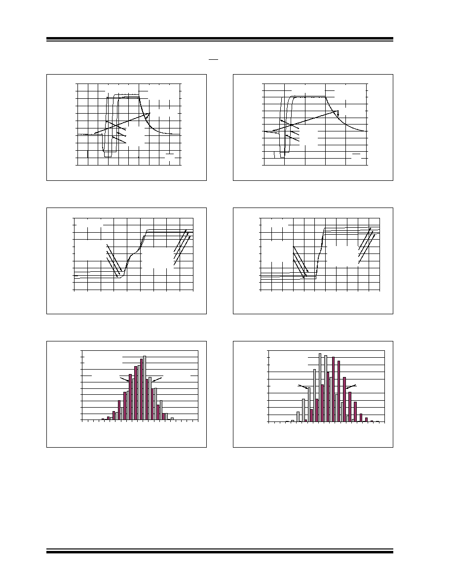
FIGURE 2-40:
THD plus Noise vs. Load
Resistance.
FIGURE 2-41:
Gain Select Timing, with
Gain = 1 and 50.
FIGURE 2-42:
Gain Select Timing, with
Gain = 1 and 10.
0.001
0.01
0.1
1
10
1.5
2.0
2.5
3.0
3.5
4.0
4.5
5.0
5.5
Power Supply Voltage (V)
TH
D + Noise
(%)
G = +1
G = +10
G = +50
V
OUT
= 0.8V
DD
f = 1 kHz
Measurement BW = 80 kHz
0.001
0.01
0.1
1
10
1
10
Output Swing (V
P-P
)
TH
D + No
i
se (%
)
G = +1
G = +10
G = +50
Measurement BW = 80 kHz
V
DD
= 5.0V
f = 1 kHz
0.0
0.5
1.0
1.5
2.0
2.5
3.0
3.5
4.0
4.5
5.0
0
10
20
30
40
50
60
70
80
90
100
Time (10 µs/div)
O
u
t
p
u
t
Vo
lt
ag
e (
V
)
-40
-35
-30
-25
-20
-15
-10
-5
0
5
10
G
a
in S
e
le
ct
Volt
a
g
e
(
V
)
0
GSEL
(G = +1)
(G = +10)
(G = +10)
5
V
DD
= 5.0V
V
IN
= 0.15V
V
OUT
0.001
0.01
0.1
1
10
1.E+03
1.E+04
1.E+05
1.E+06
Load Resistance ()
TH
D + Nois
e (%)
G = +1
G = +10
G = +50
f = 1 kHz
V
DD
= 5.0V
1k
10k
100k
1M
Measurement BW = 80 kHz
0.0
0.5
1.0
1.5
2.0
2.5
3.0
3.5
4.0
4.5
5.0
0
10
20
30
40
50
60
70
80
90
100
Time (10 µs/div)
O
u
tp
u
t
Vo
lt
ag
e
(
V
)
-40
-35
-30
-25
-20
-15
-10
-5
0
5
10
G
a
in S
e
le
ct
Volt
a
g
e
(
V
)
0
GSEL
(G = +1)
(G = +50)
(G = +1)
5
V
DD
= 5.0V
V
IN
= 0.030V
V
OUT
0.0
0.5
1.0
1.5
2.0
2.5
3.0
3.5
4.0
4.5
5.0
0
10
20
30
40
50
60
70
80
90
100
Time (10 µs/div)
O
u
t
p
u
t
Vo
lt
ag
e (V
)
-40
-35
-30
-25
-20
-15
-10
-5
0
5
10
Ga
in
Se
lec
t
Volt
age (
V
)
0
GSEL
(G = +10)
(G = +50)
(G = +10)
5
V
DD
= 5.0V
V
IN
= 0.030V
V
OUT
MCP6G01/2/3/4
DS22004A-page 16
© 2006 Microchip Technology Inc.
Note: Unless otherwise indicated, T
A
= +25°C, V
DD
= +1.8V to +5.5V, V
SS
= GND, G = +1 V/V, V
IN
= (0.3V)/G,
R
L
= 100 k
to V
DD
/2, C
L
= 60 pF, GSEL = V
DD
/2, and CS is tied low.
FIGURE 2-43:
Output Voltage vs. Chip
Select, with V
DD
= 1.8V.
FIGURE 2-44:
GSEL Pin Current vs. GSEL
Voltage, with V
DD
= 1.8V.
FIGURE 2-45:
GSEL Current, with GSEL
Voltage of 0.3V
DD
.
FIGURE 2-46:
Output Voltage vs. Chip
Select, with V
DD
= 5.0V.
FIGURE 2-47:
GSEL Pin Current vs. GSEL
Voltage, with V
DD
= 5.5V.
FIGURE 2-48:
GSEL Current, with GSEL
Voltage of 0.7V
DD
.
-0.2
0.0
0.2
0.4
0.6
0.8
1.0
1.2
1.4
1.6
1.8
2.0
Time (20 µs/div)
Outp
ut V
o
lt
age
(mV)
Ch
ip
S
e
le
ct
V
o
l
t
a
g
e
(V
)
1.8
0
V
OUT
is "ON"
CS
V
DD
= 1.8V
V
IN
= 0.9V
DD
Shutdown
G = 1
G = 10
G = 50
-10
-8
-6
-4
-2
0
2
4
6
8
10
0.0
0.2
0.4
0.6
0.8
1.0
1.2
1.4
1.6
1.8
GSEL Voltage (V)
GS
E
L
Cu
rre
n
t (µA
)
T
A
= +25°C
= +85°C
= +125°C
V
DD
= 1.8V
T
A
= +125°C
= +85°C
= +25°C
0%
2%
4%
6%
8%
10%
12%
14%
16%
18%
20%
22%
-7
.0
-6
.6
-6
.2
-5
.8
-5
.4
-5
.0
-4
.6
-4
.2
-3
.8
-3
.4
-3
.0
GSEL Current (µA)
Perc
en
t
a
g
e
o
f
O
ccu
rre
nc
es
1228 Samples
GSEL = 0.3V
DD
V
DD
= 1.8V
V
DD
= 5.5V
-0.5
0.0
0.5
1.0
1.5
2.0
2.5
3.0
3.5
4.0
4.5
5.0
5.5
Time (20 µs/div)
Outp
ut V
o
lt
age
(mV)
Ch
ip
S
e
le
ct
V
o
l
t
a
g
e
(V
)
5
0
V
OUT
is "ON"
CS
V
DD
= 5.0V
V
IN
= 0.9V
DD
Shutdown
G = 1
G = 10
G = 50
-10
-8
-6
-4
-2
0
2
4
6
8
10
0.0 0.5 1.0 1.5 2.0 2.5 3.0 3.5 4.0 4.5 5.0 5.5
GSEL Voltage (V)
GS
E
L
Cu
rre
n
t (µA
)
V
DD
= 5.5V
T
A
= +25°C
= +85°C
= +125°C
T
A
= +125°C
= +85°C
= +25°C
0%
2%
4%
6%
8%
10%
12%
14%
16%
18%
20%
3.
0
3.
4
3.
8
4.
2
4.
6
5.
0
5.
4
5.
8
6.
2
6.
6
7.
0
GSEL Current (µA)
Pe
rcen
t
a
g
e
of
Occ
u
r
r
en
ce
s
1228 Samples
GSEL = 0.7V
DD
V
DD
= 5.5V
V
DD
= 1.8V
© 2006 Microchip Technology Inc.
DS22004A-page 17
MCP6G01/2/3/4
Note: Unless otherwise indicated, T
A
= +25°C, V
DD
= +1.8V to +5.5V, V
SS
= GND, G = +1 V/V, V
IN
= (0.3V)/G,
R
L
= 100 k
to V
DD
/2, C
L
= 60 pF, GSEL = V
DD
/2, and CS is tied low.
FIGURE 2-49:
GSEL Trip Point between
G = +1 and G = +10.
FIGURE 2-50:
GSEL Trip Point between
G = +1 and G = +50.
0%
10%
20%
30%
40%
50%
60%
70%
80%
90%
100%
0.
2
1
3
0.
2
1
8
0.
2
2
2
0.
2
2
7
0.
2
3
1
0.
2
3
6
0.
2
4
1
0.
2
4
5
0.
2
5
0
0.
2
5
5
0.
2
5
9
Normalized GSEL Trip Point; V
GSEL
/V
DD
Pe
rce
n
t
a
ge
o
f
O
ccu
rre
n
ces
1227 Samples
G = +1 to +10
V
DD
= 1.8V
V
DD
= 5.5V
0%
10%
20%
30%
40%
50%
60%
70%
80%
90%
100%
0.
7
3
6
0.
7
4
1
0.
7
4
5
0.
7
5
0
0.
7
5
5
0.
7
5
9
0.
7
6
4
0.
7
6
8
0.
7
7
3
Normalized GSEL Trip Point; V
GSEL
/V
DD
Perc
en
t
a
g
e
of
Occ
u
r
r
en
ce
s
1228 Samples
G = +1 to +50
V
DD
= 1.8V
V
DD
= 5.5V
MCP6G01/2/3/4
DS22004A-page 18
© 2006 Microchip Technology Inc.
3.0
PIN DESCRIPTIONS
Descriptions of the pins are listed in
Table 3-1
.
TABLE 3-1:
PIN FUNCTION TABLE
3.1
Analog Output
The output pin (V
OUT
) is a low impedance voltage
source. The selected gain (G) and input voltage (V
IN
)
determine its value.
3.2
Analog Input
The analog inputs (V
IN
) are high impedance CMOS
inputs with low bias currents. Only three fixed, non-
inverting gains are available through these inputs.
3.3
Power Supply (V
SS
and V
DD
)
The Positive Power Supply Pin (V
DD
) is 1.8V to 5.5V
higher than the Negative Power Supply Pin (V
SS
). For
normal operation, the other pins are at voltages
between V
SS
and V
DD
.
Typically, these parts are used in a single (positive)
supply configuration. In this case, V
SS
is connected to
ground, and V
DD
is connected to the supply. V
DD
will
need a local bypass capacitor (typically 0.01 µF to
0.1 µF) within 2 mm of the V
DD
pin. These parts need
to use a bulk capacitor (typically 1.0 µF to 10 µF) within
100 mm of the V
DD
pin; it can be shared with nearby
analog parts.
3.4
Digital Inputs
The Chip Select (CS) input is a Schmitt-triggered,
CMOS logic input.
The Gain Select (GSEL) inputs are tri-level digital
inputs. They function similar to normal logic inputs at
low (G = +10) and high voltages (G = +50). The pin can
also be set to mid-supply (G = +1) by a low impedance
source, or by leaving this pin open.
MCP6G01
MCP6G02
MCP6G03
MCP6G04
Symbol
Description
6
1
6
1
V
OUT
, V
OUTA
Analog Output (SGA A)
2
2
2
2
GSEL, GSEL
A
Gain Select Input (SGA A)
3
3
3
3
V
IN
, V
INA
Analog Input (SGA A)
7
8
7
4
V
DD
Positive Power Supply
--
5
--
5
V
INB
Analog Input (SGA B)
--
6
--
6
GSEL
B
Gain Select Input (SGA B)
--
7
--
7
V
OUTB
Analog Output (SGA B)
--
--
--
8
V
OUTC
Analog Output (SGA C)
--
--
--
9
GSEL
C
Gain Select Input (SGA C)
--
--
--
10
V
INC
Analog Input (SGA C)
4
4
4
11
V
SS
Negative Power Supply
--
--
--
12
V
IND
Analog Input (SGA D)
--
--
--
13
GSEL
D
Gain Select Input (SGA D)
--
--
--
14
V
OUTD
Analog Output (SGA D)
--
--
8
--
CS
Chip Select
1, 5, 8
--
1, 5
--
NC
No Internal Connection
© 2006 Microchip Technology Inc.
DS22004A-page 19
MCP6G01/2/3/4
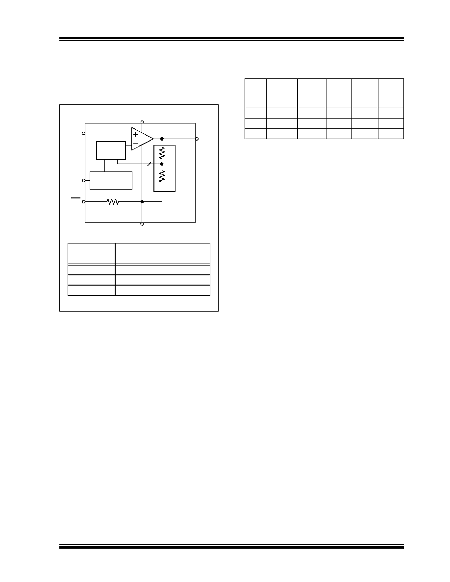
4.0
APPLICATIONS INFORMATION
The MCP6G01/2/3/4 family of Selectable Gain
Amplifiers (SGA) is based on simple analog building
blocks (see
Figure 4-1
). Each of these blocks will be
explained in more detail in the following subsections.
FIGURE 4-1:
SGA Block Diagram.
4.1
Internal Op Amp
The internal op amp gives the right combination of
bandwidth, accuracy, and flexibility.
4.1.1
COMPENSATION CAPACITORS
The internal op amp has three compensation
capacitors (comp. caps.) connected to a switching
network. They are selected to give good small signal
bandwidth at high gains, and good slew rate (full power
bandwidth) at low gains. The change in bandwidth as
gain changes is between 250 and 900 kHz. Refer to
Table 4-1
for more information.
TABLE 4-1:
GAIN VS. INTERNAL
COMPENSATION
CAPACITOR
4.1.2
RAIL-TO-RAIL INPUTS
The input stage of the internal op amp uses two
differential input stages in parallel; one operates at low
V
IN
(input voltage), while the other operates at high V
IN
.
With this topology, the internal inputs can operate to
0.3V past either supply rail, although the output will clip
the signal before that happens.
The transition between the two input stage occurs
when V
IN
V
DD
1.1V (see
Figure 2-19
and
Figure 2-
22
). For the best distortion and gain linearity, avoid this
region of operation.
4.1.3
PHASE REVERSAL
The MCP6G01/2/3/4 amplifier family is designed with
CMOS input devices. It is designed to not exhibit phase
inversion when the input pins exceed the supply
voltages.
Figure 2-7
shows an input voltage exceeding
both supplies with no resulting phase inversion.
4.1.4
INPUT VOLTAGE AND CURRENT
LIMITS
The ESD protection on the inputs can be depicted as
shown in
Figure 4-2
. This structure was chosen to
protect the input transistors, and to minimize input bias
current (I
B
). The input ESD diodes clamp the inputs
when they try to go more than one diode drop below
V
SS
. They also clamp any voltages that go too far
above V
DD
; their breakdown voltage is high enough to
allow normal operation, and low enough to bypass ESD
events within the specified limits.
Gain
(V/V)
GSEL Voltage (Typ.)
(V)
1
V
DD
/2 (or open)
10
0
50
V
DD
Note:
V
SS
is assumed to be 0V
V
OUT
V
DD
GSEL
V
IN
V
SS
3
R
F
R
G
Gain Select
Logic
Gain
Switches
Re
sisto
r
L
adde
r
(R
LAD
)
CS
(MCP6G03
only)
5 M
Gain
(V/V)
Internal
Comp.
Cap.
G x BW
(MHz)
Typ.
SR
(V/µs)
Typ.
FPBW
(kHz)
Typ.
BW
(kHz)
Typ.
1
Large
0.90
0.50
29
900
10
Medium
3.5
2.3
133
350
50
Small
12.5
4.5
260
250
Note 1:
Changing the compensation capacitor does not
change the DC performance (e.g., V
OS
).
2:
G x BW is approximately the Gain Bandwidth
Product of the internal op amp.
3:
FPBW is the Full Power Bandwidth at
V
DD
= 5.5V, which is based on slew rate (SR).
4:
BW is the closed-loop, small signal 3 dB
bandwidth.
MCP6G01/2/3/4
DS22004A-page 20
© 2006 Microchip Technology Inc.
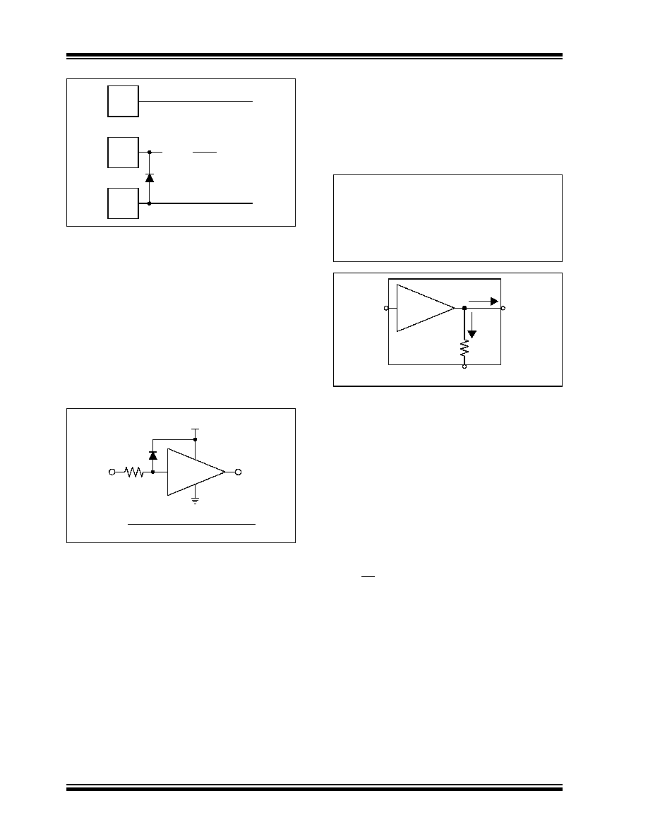
FIGURE 4-2:
Simplified Analog Input ESD
Structures.
In order to prevent damage and/or improper operation
of these amplifiers, the circuits they are in must limit the
currents (and voltages) at the V
IN
pins (see Section
"Absolute Maximum Ratings " at the beginning of
Section 1.0 "Electrical Characteristics").
Figure 4-3
shows the recommended approach to protecting these
inputs. The internal ESD diodes prevent the input pins
(V
IN
) from going too far below ground, and the resistor
R
1
limits the possible current drawn out of the input pin.
Diode D
1
prevents the input pin (V
IN
) from going too far
above V
DD
. When implemented as shown, resistor R
1
also limits the current through D
1
.
FIGURE 4-3:
Protecting the Analog
Inputs.
It is also possible to connect the diode to the left of the
resistor R
1
. In this case, the current through the diode
D
1
needs to be limited by some other mechanism. The
resistor then serves as in-rush current limiter; the DC
current into the input pin (V
IN
) should be very small.
A significant amount of current can flow out of the
inputs when the common mode voltage (V
CM
) is below
ground (V
SS
); see
Figure 2-17
. Applications that are
high impedance may need to limit the useable voltage
range.
4.1.5
RAIL-TO-RAIL OUTPUT
The maximum output voltage swing is the maximum
swing possible under a particular amplifier load current.
The amplifier load current is the sum of the external
load current (I
OUT
) and the current through the ladder
resistance (I
LAD
); see
Figure 4-4
.
EQUATION 4-1:
FIGURE 4-4:
Amplifier Load Current.
See
Figure 2-20
for the typical output headroom
(V
DD
V
OH
or V
OL
V
SS
) as a function of amplifier
load current.The specification table states the output
can reach within 10 mV of either supply rail when
R
L
= 100 k
.
4.2
Resistor Ladder
The resistor ladder shown in
Figure 4-1
(R
LAD
= R
F
+ R
G
) sets the gain. Placing the gain
switches in series with the inverting input reduces the
parasitic capacitance, distortion, and gain mismatch.
R
LAD
is an additional load on the output of the SGA and
causes additional current draw from the supplies.
When CS is high, the SGA is shut down (low power).
R
LAD
is still attached to the V
OUT
and V
SS
pins. Thus,
these pins and the internal amplifier's inverting input
are all connected through R
LAD
and the output is not
high-Z (unlike the internal op amp).
R
LAD
contributes to the output noise; see
Figure 2-9
.
R
LAD
is intended to be driven at the V
SS
pin by a low
impedance voltage source. The power supply driving
the V
SS
pin should have an output impedance less than
0.1
to maintain reasonable gain accuracy.
Bond
Pad
Bond
Pad
Bond
Pad
V
DD
V
IN
V
SS
to the rest of
Input
Stage
the amplifier
V
1
MCP6G0X
R
1
V
DD
D
1
R
1
V
SS
(minimum expected V
1
)
2 mA
V
OUT
V
IN
Where:
Amplifier Load Current
I
OUT
I
LAD
+
=
I
LAD
V
OUT
V
SS
(
)
R
LAD
---------------------------------
=
V
OUT
V
SS
R
LAD
I
OUT
I
LAD
MCP6G0X
V
IN
© 2006 Microchip Technology Inc.
DS22004A-page 21
MCP6G01/2/3/4
4.3
MCP6G03 Chip Select (CS)
The MCP6G03 is a single amplifier with chip select
(CS). When CS is high, the internal op amp is shut
down and its output placed in a high-Z state. The
resistive ladder is always connected between V
SS
and
V
OUT
; even in shutdown. This means that the output
resistance will be 350 k
(typ.), with a path for output
signals to appear at the input. The supply current at
V
SS
includes the current through the load resistor and
ladder resistors; it also includes current from the CS pin
to V
SS
. When CS is low, the amplifier is enabled. If CS
is left floating, the amplifier may not operate properly.
Figure 1-2
and
Figure 2-43
show how the output
voltage and supply current response to a CS pulse.
4.4
Gain Select (GSEL)
The amplifier can be set to the gains +1 V/V, +10 V/V,
and +50 V/V using one input pin (GSEL). At the same
time, different compensation capacitors are selected to
optimize the bandwidth vs. slew rate trade-off (see
Table 4-1
).
Table 4-2
shows how to change the gain
using a GPIO pin on a microcontroller and
Table 4-3
shows how to hard wire the gain (i.e., using PCB
wiring).
TABLE 4-2:
MCU DRIVEN GAIN
SELECTION
TABLE 4-3:
HARD WIRED GAIN
SELECTION
4.5
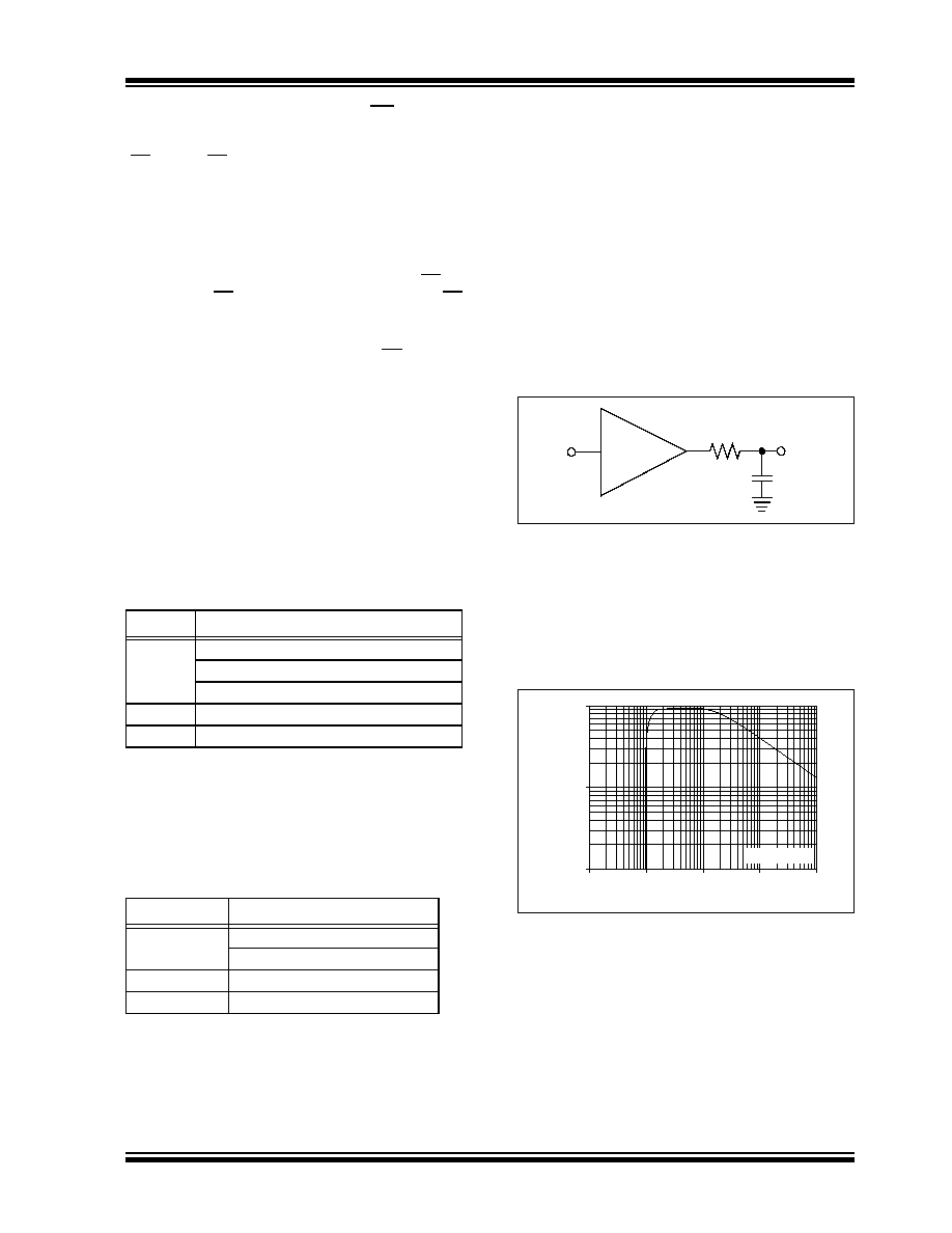
Capacitive Load and Stability
Large capacitive loads can cause stability problems
and reduced bandwidth for the MCP6G01/2/3/4 family
of SGAs (
Figure 2-30
and
Figure 2-34
). As the load
capacitance increases, there is a corresponding
increase in frequency response peaking and step
response overshoot and ringing. This happens
because a large load capacitance decreases the
internal amplifier's phase margin and bandwidth.
When driving large capacitive loads with these SGAs
(i.e., > 60 pF), a small series resistor at the output
(R
ISO
in
Figure 4-5
) improves the internal amplifier's
stability by making the load resistive at higher
frequencies. The bandwidth will be generally lower
than the bandwidth with no capacitive load.
FIGURE 4-5:
SGA Circuit for Large
Capacitive Loads.
Figure 4-6
gives recommended R
ISO
values for
different capacitive loads. After selecting R
ISO
for your
circuit, double check the resulting frequency response
peaking and step response overshoot on the bench.
Modify R
ISO
's value until the response is reasonable at
all gains.
FIGURE 4-6:
Recommended R
ISO
.
Gain
MCU Pin's State
+1 V/V
Output PIC's V
REF
at V
DD
/2
Digital Output High-Z (Notes 1)
Output V
DD
/2 PWM signal (Notes 2)
+10 V/V
Digital Output driven Low
+50 V/V
Digital Output driven High
Note 1: See Section 4.8.1 "Driving the Gain
Select Pin with a Microcontroller GPIO
Pin".
2: See Section 4.8.2 "Driving the Gain
Select Pin with a PWM Signal"
Selected Gain
Possible GSEL Drivers
+1 V/V
Open Circuit (Note 1)
Low impedance source at V
DD
/2
+10 V/V
Tied to GND (0V)
+50 V/V
Tied to V
DD
Note 1: The GSEL pin floats to mid-supply
(V
DD
/2); a bypass capacitor may be
needed.
V
IN
V
OUT
MCP6G0X
R
ISO
C
L
10
100
1,000
10
100
1,000
10,000
100,000
Load Capacitance (F)
Recommended R
ISO
(
)
10p
100p
1n
100n
For all gains
10n
MCP6G01/2/3/4
DS22004A-page 22
© 2006 Microchip Technology Inc.
4.6
Layout Considerations
Good PC board layout techniques will help achieve the
performance shown in Section 1.0 "Electrical
Characteristics" and Section 2.0 "Typical
Performance Curves". It will also help minimize
Electromagnetic Compatibility (EMC) issues.
Because the MCP6G01/2/3/4 SGAs' frequency
response reaches unity gain at 10 MHz when G = 50, it
is important to use good PCB layout techniques. Any
parasitic coupling at high frequency might cause
undesired peaking. Filtering high frequency signals
(i.e., fast edge rates) can help.
4.6.1
COMPONENT PLACEMENT
Separate different circuit functions: digital from analog,
low speed from high speed, and low power from high
power. This will reduce crosstalk.
Keep sensitive traces short and straight. Separate
them from interfering components and traces. This is
especially important for high frequency (low rise time)
signals.
4.6.2
SUPPLY BYPASS
Use a local bypass capacitor (0.01 µF to 0.1 µF) within
2 mm of the V
DD
pin for good, high frequency
performance. It must connect directly to ground.
Use a bulk bypass capacitor (i.e., 1.0 µF to 10 µF)
within 100 mm of the V
DD
pin. It needs to connect to
ground, and provides large, slow currents. This
capacitor may be shared with other nearby analog
parts.
Ground plane is important, and power plane(s) can
also be of great help. High frequency (e.g., multi-layer
ceramic capacitors), surface mount components
improve the supply's performance.
4.6.3
INPUT SOURCE IMPEDANCE
The sources driving the inputs of the SGAs need to
have reasonably low source impedance at higher
frequencies.
Figure 4-7
shows how the external source
resistance (R
S
), SGA package pin capacitance (C
P1
),
and SGA package pin-to-pin capacitance (C
P2
) form a
positive feedback voltage divider network. Feedback
may cause frequency response peaking and step
response overshoot and ringing.
FIGURE 4-7:
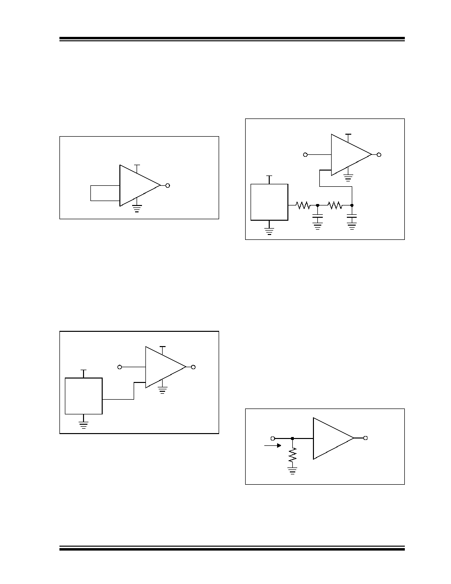
Positive Feedback Path.
Figure 2-10
shows the crosstalk (referred to input) that
results when a hostile signal is connected to the other
inputs (e.g., V
INB
through V
IND
), and the input of
interest (e.g., V
INA
) has R
S
connected to GND. A gain
of +50 was chosen for this plot because it
demonstrates the worst-case behavior. Increasing R
S
increases the crosstalk as expected. At a source
impedance of 10 M
, there is noticeable change in
behavior.
Most designs should use a source resistance (R
S
) no
larger than 10 M
. Careful attention to layout parasitics
and proper component selection will help minimize this
effect. When a source impedance larger than 10 M
must be used, place a capacitor in parallel to C
P1
to
reduce the positive feedback. This capacitor needs to
be large enough to overcome gain (or crosstalk)
peaking, yet small enough to allow a reasonable signal
bandwidth.
4.6.4
SIGNAL COUPLING
The input pins of the MCP6G01/2/3/4 family of SGAs
are high impedance. This makes them especially
susceptible to capacitively coupled noise. Using a
ground plane helps reduce this problem.
When noise is capacitively coupled, the ground plane
provides additional shunt capacitance to ground. When
noise is magnetically coupled, the ground plane
reduces the mutual inductance between traces.
Increasing the separation between traces makes a
significant difference.
Changing the direction of one of the traces can also
reduce magnetic coupling. It may help to locate guard
traces next to the victim trace. They should be on both
sides of, and as close as possible to, the victim trace.
Connect the guard traces to the ground plane at both
ends. Also connect long guard traces to the ground
plane in the middle.
V
S
MCP6G0X
V
OUT
R
S
C
P1
C
P2
© 2006 Microchip Technology Inc.
DS22004A-page 23
MCP6G01/2/3/4
4.7
Unused Amplifiers
An unused amplifier in a quad package (MCP6G04)
should be configured as shown in
Figure 4-8
. This
circuit prevents the output from toggling and causing
crosstalk. Because the V
IN
pin looks like an open
circuit, the GSEL voltage is automatically set at V
DD
/2,
and the gain is 1 V/V. The output pin provides a
buffered V
DD
/2 voltage and minimizes the supply
current draw of the unused amplifier.
FIGURE 4-8:
Unused Amplifiers.
4.8
Typical Applications
4.8.1
DRIVING THE GAIN SELECT PIN
WITH A MICROCONTROLLER GPIO
PIN
The circuit in
Figure 4-9
uses a microcontroller GPIO
pin to drive the Gain Select input (GSEL). Setting the
GPIO pin to logic low, high-Z or logic high gives a GSEL
voltage of 0V, V
DD
/2 or V
DD
, respectively (G = 10, 1 or
50).
FIGURE 4-9:
Driving the GSEL Pin.
The microcontroller's GPIO pin cannot produce a
leakage current of more than ±1 µA for this circuit to
function properly. In noisy environments, a capacitor
may need to be added to the GPIO pin.
4.8.2
DRIVING THE GAIN SELECT PIN
WITH A PWM SIGNAL
The circuit in
Figure 4-10
uses a PWM output on a PIC
microcontroller (100 kHz clock rate) to drive the Gain
Select input (GSEL). Setting the PWM duty cycle to
0%, 50% or 100% gives a GSEL voltage of 0V, V
DD
/2
or V
DD
, respectively (G = 10, 1 or 50).
FIGURE 4-10:
Driving the GSEL Pin.
The PWM clock rate needs to be fast so it is easily
filtered and does not interfere with the desired signal,
and it needs to be slow enough for good accuracy and
low crosstalk. This filter reduces the ripple at the GSEL
pin to about 7 mV
P-P
at V
DD
= 5.0V. The 10% settling
time is about 200 µs; the filter limits how quickly the
gain can be changed. Scale the resistors and/or
capacitors for other clock rates, or for different ripple.
4.8.3
GAIN RANGING
Figure 4-11
shows a circuit that measures the current
I
X
. The circuit's performance benefits from changing
the gain on the SGA. Just as a hand-held multimeter
uses different measurement ranges to obtain the best
results, this circuit makes it easy to set a high gain for
small signals and a low gain for large signals. As a
result, the required dynamic range at the SGA's output
is less than at its input (by up to 34 dB).
FIGURE 4-11:
Wide Dynamic Range
Current Measurement Circuit.
¼ MCP6G04
V
OUT
MCP6G0X
V
IN
GSEL
V
DD
V
OUT
MCP6G0X
V
IN
GSEL
MCU
GPIO
Pin
V
DD
V
DD
V
OUT
MCP6G0X
V
IN
GSEL
PIC MCU
PWM
Output
4.7 nF
V
DD
V
DD
10 k
4.7 nF
10 k
I
X
V
OUT
MCP6G0X
R
S
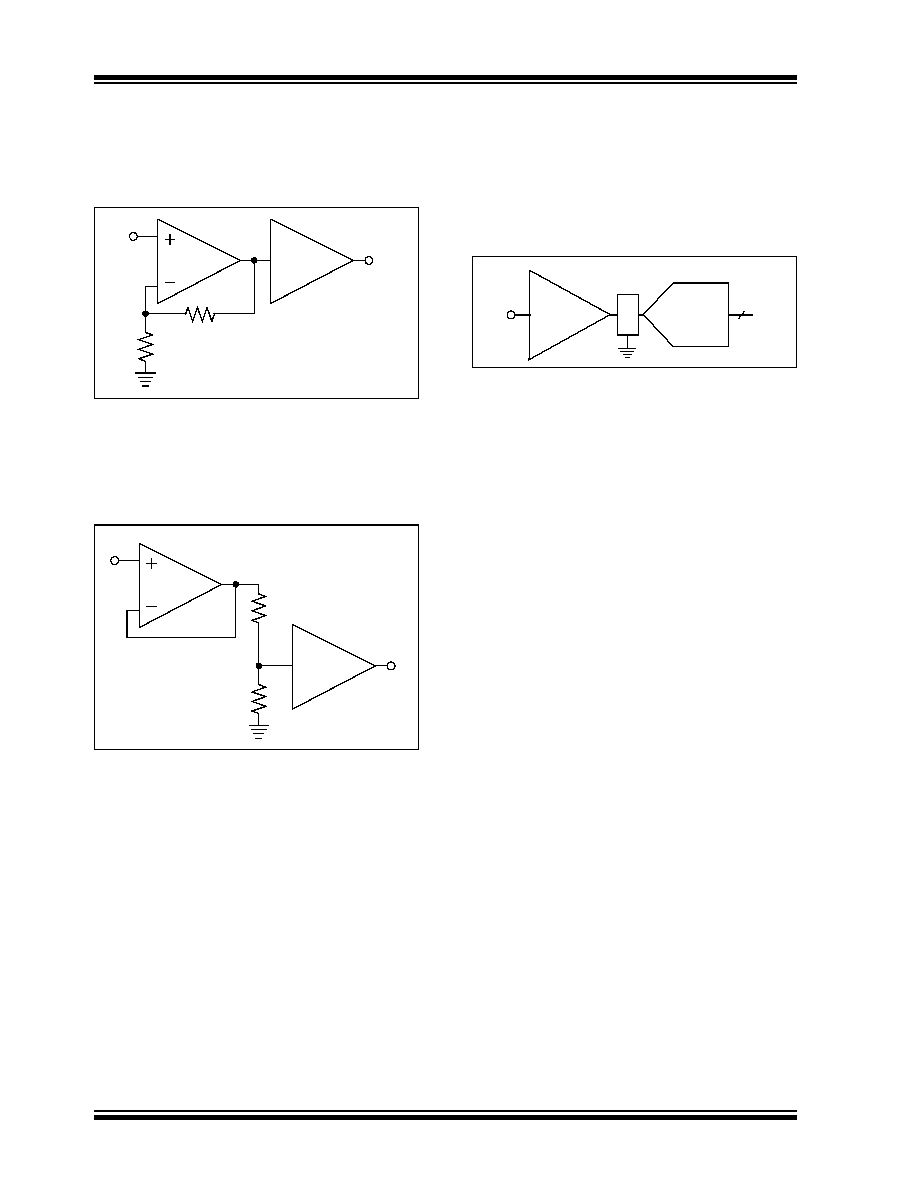
MCP6G01/2/3/4
DS22004A-page 24
© 2006 Microchip Technology Inc.
4.8.4
SHIFTED GAIN RANGE SGA
Figure 4-12
shows a circuit using a MCP6271 at a gain
of +10 in front of a MCP6G01. This shifts the overall
gain range to +10 V/V to +500 V/V (from +1 V/V to
+50 V/V).
FIGURE 4-12:
SGA with Higher Gain
Range.
It is also easy to shift the gain range to lower gains (see
Figure 4-13
). The MCP6001 acts as a unity gain buffer,
and the resistive voltage divider shifts the gain range
down to +0.1 V/V to +5.0 V/V (from +1 V/V to +50 V/V).
FIGURE 4-13:
SGA with Lower Gain
Range.
4.8.5
ADC DRIVER
This family of SGAs is well suited for driving Analog-to-
Digital Converters (ADC). The gains (1, 10, and 50)
effectively increase the ADC's input resolution by a
factor of as large as 50 (i.e., by 5.6 bits). This works
well for applications needing relative accuracy more
than absolute accuracy (e.g., power monitoring); see
Figure 4-14
.
FIGURE 4-14:
SGA as an ADC Driver.
The low-pass filter in the block diagram reduces the
integrated noise at the MCP6G01's output and serves
as an anti-aliasing filter. This filter may be designed
using Microchip's FilterLab
®
software, available at
www.microchip.com.
V
IN
V
OUT
MCP6271
MCP6G01
1.11 k
10.0 k
V
IN
MCP6001
1.11 k
10.0 k
V
OUT
MCP6G01
OUT
MCP3001
10-bit
ADC
3
MCP6G01
V
IN
Low-pass
Filter
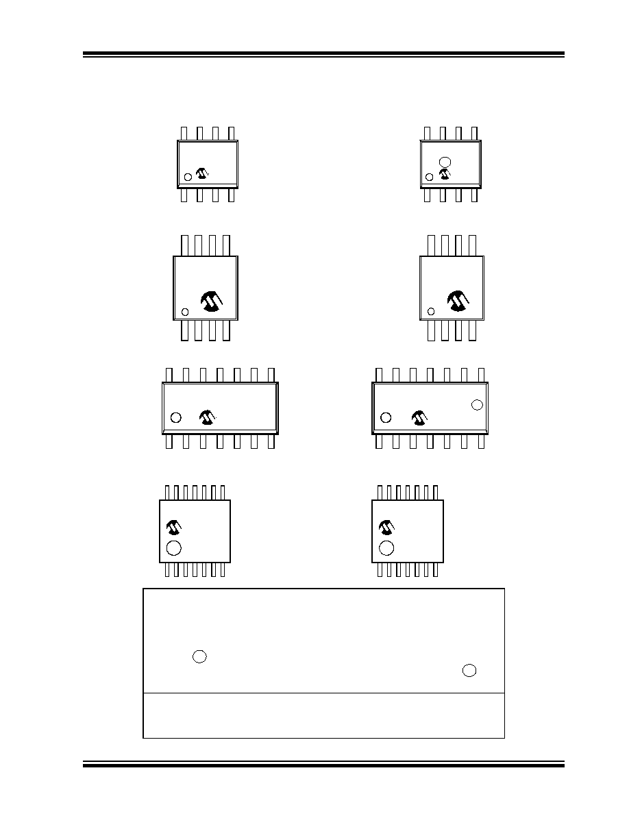
© 2006 Microchip Technology Inc.
DS22004A-page 25
MCP6G01/2/3/4
5.0
PACKAGING INFORMATION
5.1
Package Marking Information
8-Lead SOIC (150 mil) (MCP6G01, MCP6G02, MCP6G03)
Example:
XXXXXXXX
XXXXYYWW
NNN
8-Lead MSOP (MCP6G01, MCP6G02, MCP6G03)
Example:
XXXXXX
YWWNNN
6G01E
634256
MCP6G01E
SN^^0634
256
Legend: XX...X
Customer-specific information
Y
Year code (last digit of calendar year)
YY
Year code (last 2 digits of calendar year)
WW
Week code (week of January 1 is week `01')
NNN
Alphanumeric traceability code
Pb-free JEDEC designator for Matte Tin (Sn)
*
This package is Pb-free. The Pb-free JEDEC designator ( )
can be found on the outer packaging for this package.
Note:
In the event the full Microchip part number cannot be marked on one line, it will
be carried over to the next line, thus limiting the number of available
characters for customer-specific information.
3
e
3
e
3
e
14-Lead SOIC (150 mil) (MCP6S24)
Example:
XXXXXXXXXXX
YYWWNNN
XXXXXXXXXXX
XXXXXXXX
NNN
YYWW
14-Lead TSSOP (4.4mm) (MCP6S24)
Example:
6G04E/ST
256
0609
MCP6G04
0609256
E/SL^^
3
e
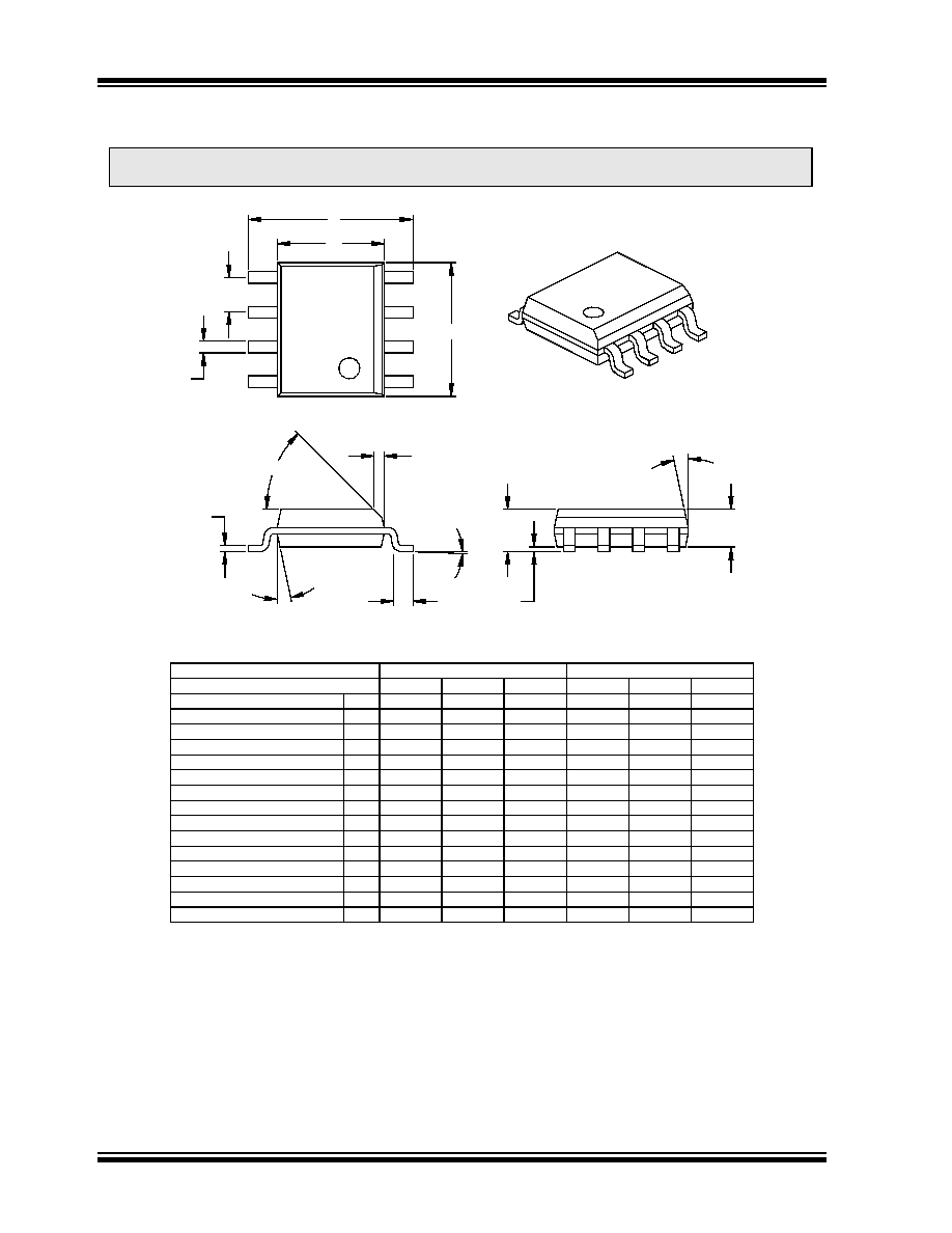
MCP6G01/2/3/4
DS22004A-page 26
© 2006 Microchip Technology Inc.
8-Lead Plastic Small Outline (SN) Narrow, 150 mil (SOIC)
Foot Angle
0
4
8
0
4
8
15
12
0
15
12
0
Mold Draft Angle Bottom
15
12
0
15
12
0
Mold Draft Angle Top
0.51
0.42
0.33
.020
.017
.013
B
Lead Width
0.25
0.23
0.20
.010
.009
.008
c
Lead Thickness
0.76
0.62
0.48
.030
.025
.019
L
Foot Length
0.51
0.38
0.25
.020
.015
.010
h
Chamfer Distance
5.00
4.90
4.80
.197
.193
.189
D
Overall Length
3.99
3.91
3.71
.157
.154
.146
E1
Molded Package Width
6.20
6.02
5.79
.244
.237
.228
E
Overall Width
0.25
0.18
0.10
.010
.007
.004
A1
Standoff §
1.55
1.42
1.32
.061
.056
.052
A2
Molded Package Thickness
1.75
1.55
1.35
.069
.061
.053
A
Overall Height
1.27
.050
p
Pitch
8
8
n
Number of Pins
MAX
NOM
MIN
MAX
NOM
MIN
Dimension Limits
MILLIMETERS
INCHES*
Units
2
1
D
n
p
B
E
E1
h
L
c
45
°
A2
A
A1
* Controlling Parameter
Notes:
Dimensions D and E1 do not include mold flash or protrusions. Mold flash or protrusions shall not exceed
.010" (0.254mm) per side.
JEDEC Equivalent: MS-012
Drawing No. C04-057
§ Significant Characteristic
Note:
For the most current package drawings, please see the Microchip Packaging Specification located at
http://www.microchip.com/packaging
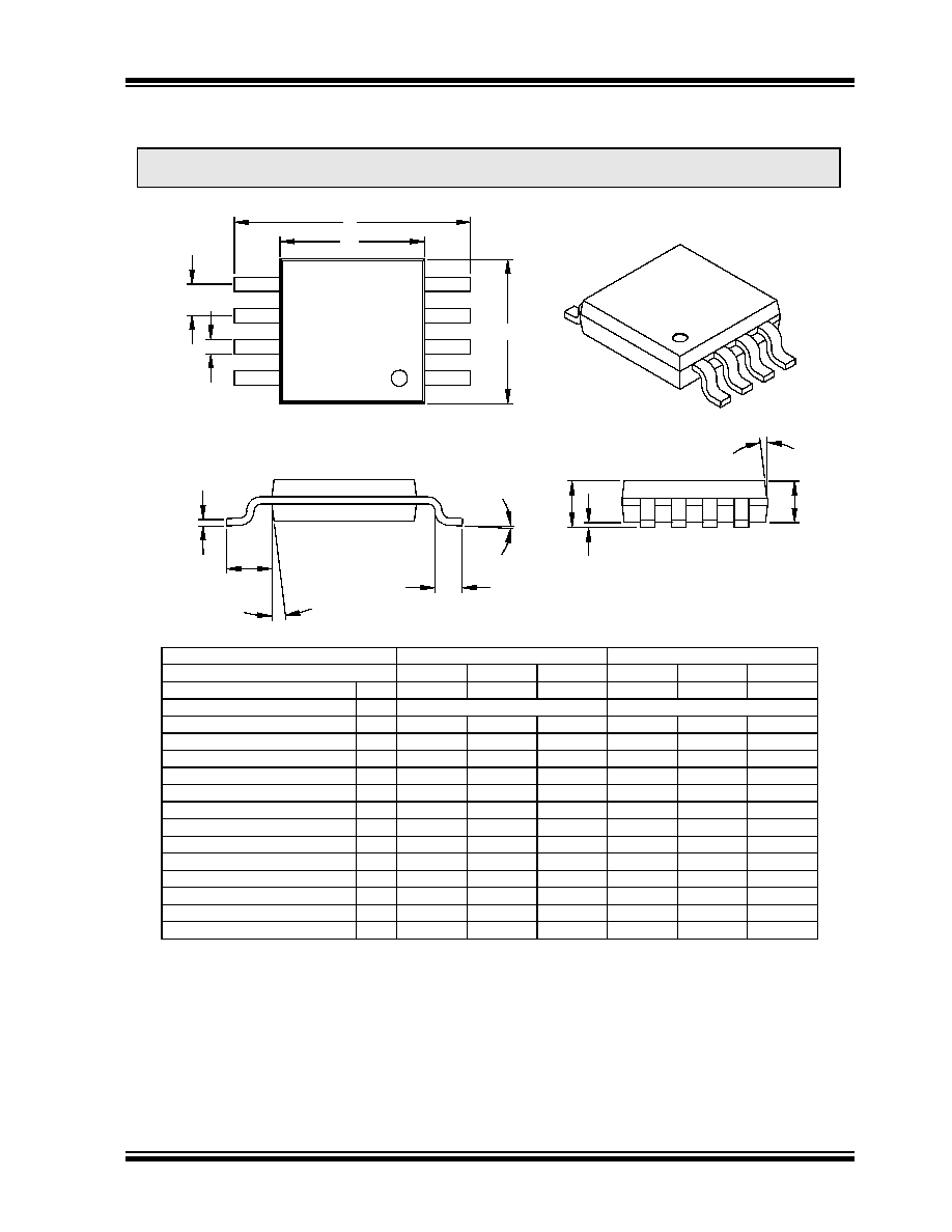
© 2006 Microchip Technology Inc.
DS22004A-page 27
MCP6G01/2/3/4
8-Lead Plastic Micro Small Outline Package (MS) (MSOP)
p
A
A1
A2
D
L
c
Dimensions D and E1 do not include mold flash or protrusions. Mold flash or protrusions shall not
.037
.035
F
Footprint (Reference)
exceed .010" (0.254mm) per side.
Notes:
Drawing No. C04-111
*Controlling Parameter
Mold Draft Angle Top
Mold Draft Angle Bottom
Foot Angle
Lead Width
Lead Thickness
c
B
7
7
.004
.010
0
.006
.012
(F)
Dimension Limits
Overall Height
Molded Package Thickness
Molded Package Width
Overall Length
Foot Length
Standoff §
Overall Width
Number of Pins
Pitch
A
L
E1
D
A1
E
A2
.016
.114
.114
.022
.118
.118
.002
.030
.193
.034
MIN
p
n
Units
.026
NOM
8
INCHES
1.00
0.95
0.90
.039
0.15
0.30
.008
.016
6
0.10
0.25
0
7
7
0.20
0.40
6
MILLIMETERS*
0.65
0.86
3.00
3.00
0.55
4.90
.044
.122
.028
.122
.038
.006
0.40
2.90
2.90
0.05
0.76
MIN
MAX
NOM
1.18
0.70
3.10
3.10
0.15
0.97
MAX
8
E1
E
B
n
1
2
§ Significant Characteristic
.184
.200
4.67
.5.08
Note:
For the most current package drawings, please see the Microchip Packaging Specification located at
http://www.microchip.com/packaging
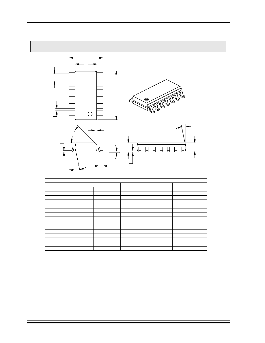
MCP6G01/2/3/4
DS22004A-page 28
© 2006 Microchip Technology Inc.
14-Lead Plastic Small Outline (SL) Narrow, 150 mil (SOIC)
Foot Angle
0
4
8
0
4
8
15
12
0
15
12
0
Mold Draft Angle Bottom
15
12
0
15
12
0
Mold Draft Angle Top
0.51
0.42
0.36
.020
.017
.014
B
Lead Width
0.25
0.23
0.20
.010
.009
.008
c
Lead Thickness
1.27
0.84
0.41
.050
.033
.016
L
Foot Length
0.51
0.38
0.25
.020
.015
.010
h
Chamfer Distance
8.81
8.69
8.56
.347
.342
.337
D
Overall Length
3.99
3.90
3.81
.157
.154
.150
E1
Molded Package Width
6.20
5.99
5.79
.244
.236
.228
E
Overall Width
0.25
0.18
0.10
.010
.007
.004
A1
Standoff §
1.55
1.42
1.32
.061
.056
.052
A2
Molded Package Thickness
1.75
1.55
1.35
.069
.061
.053
A
Overall Height
1.27
.050
p
Pitch
14
14
n
Number of Pins
MAX
NOM
MIN
MAX
NOM
MIN
Dimension Limits
MILLIMETERS
INCHES*
Units
2
1
D
p
n
B
E
E1
h
L
c
45
°
A2
A
A1
* Controlling Parameter
Notes:
Dimensions D and E1 do not include mold flash or protrusions. Mold flash or protrusions shall not exceed
.010" (0.254mm) per side.
JEDEC Equivalent: MS-012
Drawing No. C04-065
§ Significant Characteristic
Note:
For the most current package drawings, please see the Microchip Packaging Specification located at
http://www.microchip.com/packaging
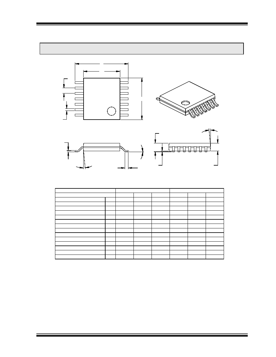
© 2006 Microchip Technology Inc.
DS22004A-page 29
MCP6G01/2/3/4
14-Lead Plastic Thin Shrink Small Outline (ST) 4.4 mm (TSSOP)
8
4
0
8
4
0
Foot Angle
10
5
0
10
5
0
Mold Draft Angle Bottom
10
5
0
10
5
0
Mold Draft Angle Top
0.30
0.25
0.19
.012
.010
.007
B1
Lead Width
0.20
0.15
0.09
.008
.006
.004
c
Lead Thickness
0.70
0.60
0.50
.028
.024
.020
L
Foot Length
5.10
5.00
4.90
.201
.197
.193
D
Molded Package Length
4.50
4.40
4.30
.177
.173
.169
E1
Molded Package Width
6.50
6.38
6.25
.256
.251
.246
E
Overall Width
0.15
0.10
0.05
.006
.004
.002
A1
Standoff §
0.95
0.90
0.85
.037
.035
.033
A2
Molded Package Thickness
1.10
.043
A
Overall Height
0.65
.026
p
Pitch
14
14
n
Number of Pins
MAX
NOM
MIN
MAX
NOM
MIN
Dimension Limits
MILLIMETERS*
INCHES
Units
L
c
2
1
D
n
B
p
E1
E
A2
A1
A
* Controlling Parameter
Notes:
Dimensions D and E1 do not include mold flash or protrusions. Mold flash or protrusions shall not exceed
.005" (0.127mm) per side.
JEDEC Equivalent: MO-153
Drawing No. C04-087
§ Significant Characteristic
Note:
For the most current package drawings, please see the Microchip Packaging Specification located at
http://www.microchip.com/packaging

MCP6G01/2/3/4
DS22004A-page 30
© 2006 Microchip Technology Inc.
NOTES:

© 2006 Microchip Technology Inc.
DS22004A-page 31
MCP6G01/2/3/4
APPENDIX A: REVISION HISTORY
Revision A (September 2006)
· Original Release of this Document.

MCP6G01/2/3/4
DS22004A-page 32
© 2006 Microchip Technology Inc.
NOTES:
© 2006 Microchip Technology Inc.
DS22004A-page 33
MCP6G01/2/3/4
PRODUCT IDENTIFICATION SYSTEM
To order or obtain information, e.g., on pricing or delivery, refer to the factory or the listed sales office
.
Device:
MCP6G01:
Single SGA
MCP6G01T: Single SGA
(Tape and Reel for MSOP and SOIC)
MCP6G02:
Dual SGA
MCP6G02T: Dual SGA
(Tape and Reel for MSOP and SOIC)
MCP6G03:
Single SGA
MCP6G03T: Single SGA
(Tape and Reel for MSOP and SOIC)
MCP6G04:
Quad SGA
MCP6G04T: Quad SGA
(Tape and Reel for SOIC and TSSOP)
Temperature Range:
E
= -40°C to +125°C
Package:
MS = Plastic MSOP, 8-lead
SN = Plastic SOIC (150 mil Body), 8-lead
SL = Plastic SOIC (150 mil Body), 14-lead (MCP6G04)
ST = Plastic TSSOP (4.4mm Body), 14-lead (MCP6G04)
PART NO.
X
/XX
Package
Temperature
Range
Device
Examples:
a)
MCP6G01-E/MS: Extended Temperature,
8LD MSOP.
b)
MCP6G01T-E/SN: Tape and Reel,
Extended Temperature,
8LD SOIC.
a)
MCP6G02-E/MS: Extended Temperature,
8LD MSOP.
b)
MCP6G02T-E/SN: Tape and Reel,
Extended Temperature,
8LD SOIC.
a)
MCP6G03-E/MS: Extended Temperature,
8LD MSOP.
b)
MCP6G03T-E/SN: Tape and Reel,
Extended Temperature,
8LD SOIC.
c)
MCP6G03-E/SN: Extended Temperature,
8LD SOIC.
a)
MCP6G04T-E/SL: Tape and Reel,
Extended Temperature,
14LD SOIC.
b)
MCP6G04T-E/ST: Tape and Reel,
Extended Temperature,
14LD TSSOP.
c)
MCP6G04-E/ST: Extended Temperature,
14LD TSSOP.

MCP6G01/2/3/4
DS22004A-page 34
© 2006 Microchip Technology Inc.
NOTES:
© 2006 Microchip Technology Inc.
DS22004A-page 35
Information contained in this publication regarding device
applications and the like is provided only for your convenience
and may be superseded by updates. It is your responsibility to
ensure that your application meets with your specifications.
MICROCHIP MAKES NO REPRESENTATIONS OR
WARRANTIES OF ANY KIND WHETHER EXPRESS OR
IMPLIED, WRITTEN OR ORAL, STATUTORY OR
OTHERWISE, RELATED TO THE INFORMATION,
INCLUDING BUT NOT LIMITED TO ITS CONDITION,
QUALITY, PERFORMANCE, MERCHANTABILITY OR
FITNESS FOR PURPOSE. Microchip disclaims all liability
arising from this information and its use. Use of Microchip
devices in life support and/or safety applications is entirely at
the buyer's risk, and the buyer agrees to defend, indemnify and
hold harmless Microchip from any and all damages, claims,
suits, or expenses resulting from such use. No licenses are
conveyed, implicitly or otherwise, under any Microchip
intellectual property rights.
Trademarks
The Microchip name and logo, the Microchip logo, Accuron,
dsPIC, K
EE
L
OQ
, microID, MPLAB, PIC, PICmicro,
PICSTART, PRO MATE, PowerSmart, rfPIC, and
SmartShunt are registered trademarks of Microchip
Technology Incorporated in the U.S.A. and other countries.
AmpLab, FilterLab, Migratable Memory, MXDEV, MXLAB,
SEEVAL, SmartSensor and The Embedded Control Solutions
Company are registered trademarks of Microchip Technology
Incorporated in the U.S.A.
Analog-for-the-Digital Age, Application Maestro, CodeGuard,
dsPICDEM, dsPICDEM.net, dsPICworks, ECAN,
ECONOMONITOR, FanSense, FlexROM, fuzzyLAB,
In-Circuit Serial Programming, ICSP, ICEPIC, Linear Active
Thermistor, Mindi, MiWi, MPASM, MPLIB, MPLINK, PICkit,
PICDEM, PICDEM.net, PICLAB, PICtail, PowerCal,
PowerInfo, PowerMate, PowerTool, REAL ICE, rfLAB,
rfPICDEM, Select Mode, Smart Serial, SmartTel, Total
Endurance, UNI/O, WiperLock and ZENA are trademarks of
Microchip Technology Incorporated in the U.S.A. and other
countries.
SQTP is a service mark of Microchip Technology Incorporated
in the U.S.A.
All other trademarks mentioned herein are property of their
respective companies.
© 2006, Microchip Technology Incorporated, Printed in the
U.S.A., All Rights Reserved.
Printed on recycled paper.
Note the following details of the code protection feature on Microchip devices:
·
Microchip products meet the specification contained in their particular Microchip Data Sheet.
·
Microchip believes that its family of products is one of the most secure families of its kind on the market today, when used in the
intended manner and under normal conditions.
·
There are dishonest and possibly illegal methods used to breach the code protection feature. All of these methods, to our
knowledge, require using the Microchip products in a manner outside the operating specifications contained in Microchip's Data
Sheets. Most likely, the person doing so is engaged in theft of intellectual property.
·
Microchip is willing to work with the customer who is concerned about the integrity of their code.
·
Neither Microchip nor any other semiconductor manufacturer can guarantee the security of their code. Code protection does not
mean that we are guaranteeing the product as "unbreakable."
Code protection is constantly evolving. We at Microchip are committed to continuously improving the code protection features of our
products. Attempts to break Microchip's code protection feature may be a violation of the Digital Millennium Copyright Act. If such acts
allow unauthorized access to your software or other copyrighted work, you may have a right to sue for relief under that Act.
Microchip received ISO/TS-16949:2002 certification for its worldwide
headquarters, design and wafer fabrication facilities in Chandler and
Tempe, Arizona, Gresham, Oregon and Mountain View, California. The
Company's quality system processes and procedures are for its
PICmicro
®
8-bit MCUs, K
EE
L
OQ
®
code hopping devices, Serial
EEPROMs, microperipherals, nonvolatile memory and analog
products. In addition, Microchip's quality system for the design and
manufacture of development systems is ISO 9001:2000 certified.

DS22004A-page 36
© 2006 Microchip Technology Inc.
AMERICAS
Corporate Office
2355 West Chandler Blvd.
Chandler, AZ 85224-6199
Tel: 480-792-7200
Fax: 480-792-7277
Technical Support:
http://support.microchip.com
Web Address:
www.microchip.com
Atlanta
Alpharetta, GA
Tel: 770-640-0034
Fax: 770-640-0307
Boston
Westborough, MA
Tel: 774-760-0087
Fax: 774-760-0088
Chicago
Itasca, IL
Tel: 630-285-0071
Fax: 630-285-0075
Dallas
Addison, TX
Tel: 972-818-7423
Fax: 972-818-2924
Detroit
Farmington Hills, MI
Tel: 248-538-2250
Fax: 248-538-2260
Kokomo
Kokomo, IN
Tel: 765-864-8360
Fax: 765-864-8387
Los Angeles
Mission Viejo, CA
Tel: 949-462-9523
Fax: 949-462-9608
Santa Clara
Santa Clara, CA
Tel: 408-961-6444
Fax: 408-961-6445
Toronto
Mississauga, Ontario,
Canada
Tel: 905-673-0699
Fax: 905-673-6509
ASIA/PACIFIC
Asia Pacific Office
Suites 3707-14, 37th Floor
Tower 6, The Gateway
Habour City, Kowloon
Hong Kong
Tel: 852-2401-1200
Fax: 852-2401-3431
Australia - Sydney
Tel: 61-2-9868-6733
Fax: 61-2-9868-6755
China - Beijing
Tel: 86-10-8528-2100
Fax: 86-10-8528-2104
China - Chengdu
Tel: 86-28-8665-5511
Fax: 86-28-8665-7889
China - Fuzhou
Tel: 86-591-8750-3506
Fax: 86-591-8750-3521
China - Hong Kong SAR
Tel: 852-2401-1200
Fax: 852-2401-3431
China - Qingdao
Tel: 86-532-8502-7355
Fax: 86-532-8502-7205
China - Shanghai
Tel: 86-21-5407-5533
Fax: 86-21-5407-5066
China - Shenyang
Tel: 86-24-2334-2829
Fax: 86-24-2334-2393
China - Shenzhen
Tel: 86-755-8203-2660
Fax: 86-755-8203-1760
China - Shunde
Tel: 86-757-2839-5507
Fax: 86-757-2839-5571
China - Wuhan
Tel: 86-27-5980-5300
Fax: 86-27-5980-5118
China - Xian
Tel: 86-29-8833-7250
Fax: 86-29-8833-7256
ASIA/PACIFIC
India - Bangalore
Tel: 91-80-4182-8400
Fax: 91-80-4182-8422
India - New Delhi
Tel: 91-11-4160-8631
Fax: 91-11-4160-8632
India - Pune
Tel: 91-20-2566-1512
Fax: 91-20-2566-1513
Japan - Yokohama
Tel: 81-45-471- 6166
Fax: 81-45-471-6122
Korea - Gumi
Tel: 82-54-473-4301
Fax: 82-54-473-4302
Korea - Seoul
Tel: 82-2-554-7200
Fax: 82-2-558-5932 or
82-2-558-5934
Malaysia - Penang
Tel: 60-4-646-8870
Fax: 60-4-646-5086
Philippines - Manila
Tel: 63-2-634-9065
Fax: 63-2-634-9069
Singapore
Tel: 65-6334-8870
Fax: 65-6334-8850
Taiwan - Hsin Chu
Tel: 886-3-572-9526
Fax: 886-3-572-6459
Taiwan - Kaohsiung
Tel: 886-7-536-4818
Fax: 886-7-536-4803
Taiwan - Taipei
Tel: 886-2-2500-6610
Fax: 886-2-2508-0102
Thailand - Bangkok
Tel: 66-2-694-1351
Fax: 66-2-694-1350
EUROPE
Austria - Wels
Tel: 43-7242-2244-3910
Fax: 43-7242-2244-393
Denmark - Copenhagen
Tel: 45-4450-2828
Fax: 45-4485-2829
France - Paris
Tel: 33-1-69-53-63-20
Fax: 33-1-69-30-90-79
Germany - Munich
Tel: 49-89-627-144-0
Fax: 49-89-627-144-44
Italy - Milan
Tel: 39-0331-742611
Fax: 39-0331-466781
Netherlands - Drunen
Tel: 31-416-690399
Fax: 31-416-690340
Spain - Madrid
Tel: 34-91-708-08-90
Fax: 34-91-708-08-91
UK - Wokingham
Tel: 44-118-921-5869
Fax: 44-118-921-5820
W
ORLDWIDE
S
ALES
AND
S
ERVICE
08/29/06
Document Outline
- 1.0 Electrical Characteristics
- 2.0 Typical Performance Curves�
- FIGURE 2-1: DC Gain Error, G�=�+1.
- FIGURE 2-2: DC Gain Error, G�³�+10.
- FIGURE 2-3: Input Offset Voltage.
- FIGURE 2-4: DC Gain Drift, G�=�+1.
- FIGURE 2-5: DC Gain Drift, G�³�+10.
- FIGURE 2-6: Input Offset Voltage Drift.
- FIGURE 2-7: The MCP6G01/2/3/4 family shows no phase reversal under overdrive.
- FIGURE 2-8: PSRR vs. Temperature.
- FIGURE 2-9: Input Noise Voltage Density vs. Frequency.
- FIGURE 2-10: Crosstalk vs. Frequency, with G = 50 (circuit in Figure�4-7).
- FIGURE 2-11: PSRR vs. Frequency.
- FIGURE 2-12: Quiescent Current vs. Supply Voltage.
- FIGURE 2-13: Quiescent Current (ISS) in Shutdown Mode vs. Supply Voltage.
- FIGURE 2-14: Input Bias Current vs. Temperature.
- FIGURE 2-15: Input Bias Current vs. Input Voltage.
- FIGURE 2-16: Quiescent Current (ISS) in Shutdown Mode vs. Temperature.
- FIGURE 2-17: Input Bias Current vs. Input Voltage.
- FIGURE 2-18: Output Short Circuit Current vs. Supply Voltage.
- FIGURE 2-19: Output Voltage Error vs. Ideal Output Voltage, with VDD�=�1.8V.
- FIGURE 2-20: Output Voltage Headroom vs. Output plus Ladder Current (circuit in Figure�4-4).
- FIGURE 2-21: Output Impedance vs. Frequency.
- FIGURE 2-22: Output Voltage Error vs. Ideal Output Voltage, with VDD�=�5.5V.
- FIGURE 2-23: Output Voltage Headroom vs. Temperature.
- FIGURE 2-24: Ladder Resistance Drift.
- FIGURE 2-25: Slew Rate vs. Temperature, with G�=�+1.
- FIGURE 2-26: Slew Rate vs. Temperature, with G�=�+10.
- FIGURE 2-27: Bandwidth vs. Resistive Load.
- FIGURE 2-28: Output Voltage Swing vs. Frequency.
- FIGURE 2-29: Slew Rate vs. Temperature, with G�=�+50.
- FIGURE 2-30: Bandwidth vs. Capacitive Load.
- FIGURE 2-31: Gain vs. Frequency.
- FIGURE 2-32: Small Signal Pulse Response.
- FIGURE 2-33: THD plus Noise vs. Frequency, VOUT = 2.8 VP-P.
- FIGURE 2-34: Gain Peaking vs. Capacitive Load.
- FIGURE 2-35: Large Signal Pulse Response.
- FIGURE 2-36: THD plus Noise vs. Frequency, VOUT = 4.0 VP-P.
- FIGURE 2-37: THD plus Noise vs. Supply Voltage.
- FIGURE 2-38: THD plus Noise vs. Output Swing.
- FIGURE 2-39: Gain Select Timing, with Gain = 1 and 10.
- FIGURE 2-40: THD plus Noise vs. Load Resistance.
- FIGURE 2-41: Gain Select Timing, with Gain = 1 and 50.
- FIGURE 2-42: Gain Select Timing, with Gain = 1 and 10.
- FIGURE 2-43: Output Voltage vs. Chip Select, with VDD�=�1.8V.
- FIGURE 2-44: GSEL Pin Current vs. GSEL Voltage, with VDD�=�1.8V.
- FIGURE 2-45: GSEL Current, with GSEL Voltage of 0.3VDD.
- FIGURE 2-46: Output Voltage vs. Chip Select, with VDD�=�5.0V.
- FIGURE 2-47: GSEL Pin Current vs. GSEL Voltage, with VDD�=�5.5V.
- FIGURE 2-48: GSEL Current, with GSEL Voltage of 0.7VDD.
- FIGURE 2-49: GSEL Trip Point between G�=�+1 and G�=�+10.
- FIGURE 2-50: GSEL Trip Point between G�=�+1 and G�=�+50.
- 3.0 Pin Descriptions
- 4.0 Applications Information
- 5.0 Packaging Information