©
1998 Microchip Technology Inc.
Preliminary
DS40197A-page 1
PIC16HV540
High-Performance RISC CPU:
∑ Only 33 single word instructions to learn
∑ All instructions are single cycle (200 ns) except for
program branches which are two-cycle
∑ Operating speed: DC - 20 MHz clock input
DC - 200 ns instruction cycle
∑ 12-bit wide instructions
∑ 8-bit wide data path
∑ Seven special function hardware registers
∑ Four-level deep hardware stack
∑ Direct, indirect and relative addressing modes for
data and instructions
Peripheral Features:
∑ 8-bit real time clock/counter (TMR0) with 8-bit
programmable prescaler
∑ Power-On Reset (POR)
∑ Brown-Out Protection
∑ Device Reset Timer (DRT) with short
RC-oscillator start up time
∑ Programmable Watchdog Timer (WDT) with its
own on-chip RC oscillator for reliable operation
∑ Sleep Timer
∑ 8 High Voltage I/O
∑ 4 Regulated I/O
∑ Wake up from SLEEP on pin change
∑ Programmable code-protection
∑ Power saving SLEEP mode
∑ Selectable oscillator options:
- RC:
Low-cost RC oscillator
- XT:
Standard crystal/resonator
- HS:
High speed crystal/resonator
- LP:
Power saving, low frequency crystal
∑ Glitch filtering on MCLR and pin change inputs
= Enhanced Features
Device
Pins
I/O
EPROM
RAM
PIC16HV540
18
12
512
25
CMOS Technology:
∑ Selectable on-chip 3V/5V Regulator
∑ Low-power, high-speed CMOS EPROM
technology
∑ Fully static design
∑ Wide-operating voltage range:
- 3.5V to 15V
∑ Temperature range:
- Commercial: 0
∞
C to 70
∞
C
- Industrial: -40
∞
C to 85
∞
C
∑ Low-power consumption
- < 2 mA typical @ 5V, 4 MHz
- 15
µ
A typical @ 3V, 32 kHz
- < 4.5
µ
A typical standby current @ 15V (with
WDT disabled), 0
∞
C to 70
∞
C
Enhanced PIC16C54 EPROM-Based 8-Bit CMOS Microcontroller
With On-Chip Voltage Regulator
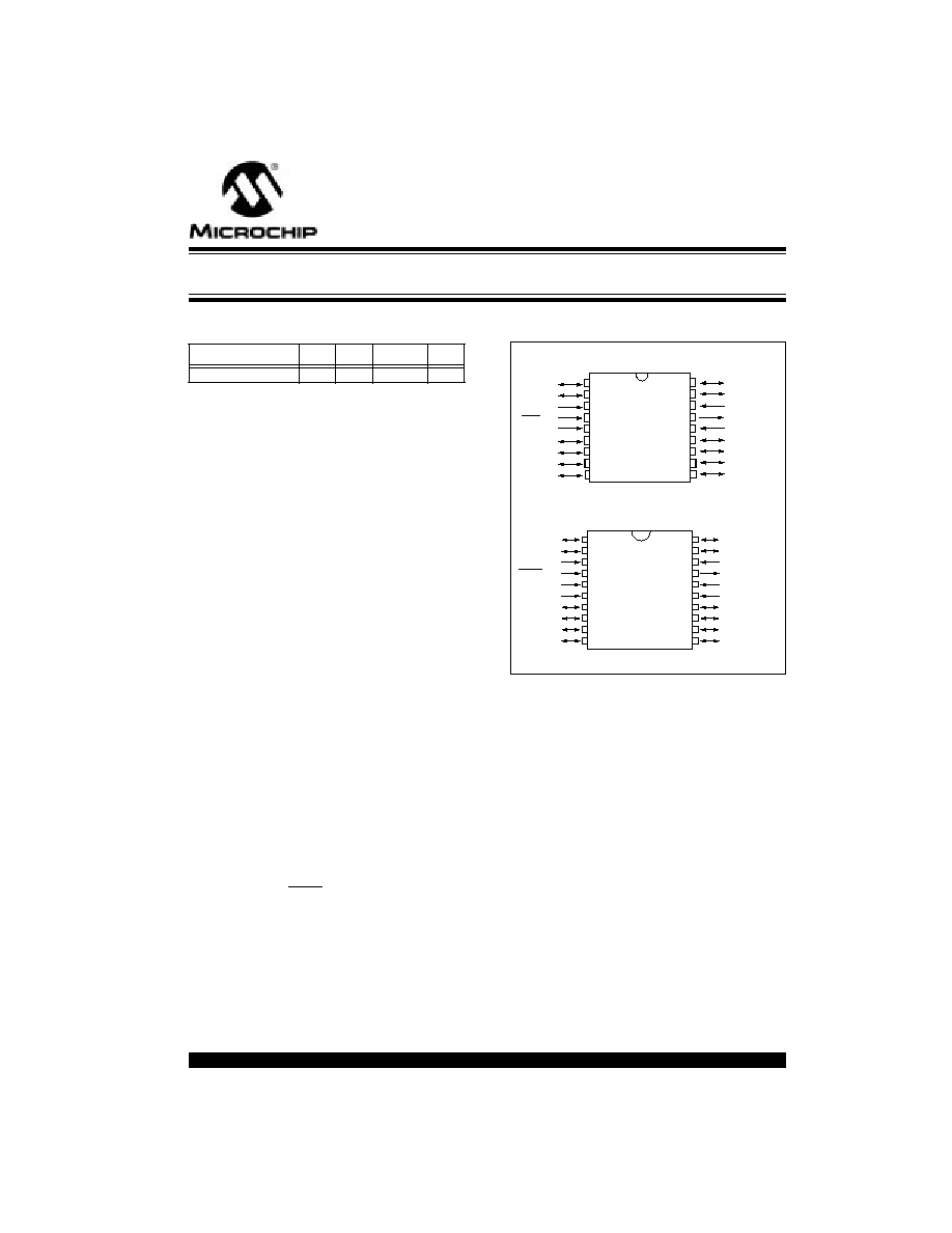
Pin Configurations
PDIP, SOIC, Windowed CERDIP
18
17
16
15
14
13
12
11
10
∑ 1
2
3
4
5
6
7
8
9
RA2
RA3
T0CKI
MCLR/V
PP
V
SS
RB0
RB1
RB2
RB3
RA1
RA0
OSC1/CLKIN
OSC2/CLKOUT
V
DD
RB7
RB6
RB5
RB4
PIC16HV540
RA1
RA0
OSC1/CLKIN
OSC2/CLKOUT
V
DD
V
DD
RB7
RB6
RB5
RB4
RA2
RA3
T0CKI
MCLR/V
PP
V
SS
V
SS
RB0
RB1
RB2
RB3
∑
1
2
3
4
5
6
7
8
9
10
20
19
18
17
16
15
14
13
12
11
SSOP
PIC16HV540
B
B
B
B
B
B
B
B
B

PIC16HV540
DS40197A-page 2
Preliminary
©
1998 Microchip Technology Inc.
1.0
GENERAL DESCRIPTION
The PIC16HV540 from Microchip Technology is a
low-cost, high-performance, 8-bit, fully-static,
EPROM-based CMOS microcontroller. It is pin and soft-
ware compatible with the PIC16C5X family of devices. It
employs a RISC architecture with only 33 single word/sin-
gle cycle instructions. All instructions are single cycle
except for program branches which take two cycles. The
PIC16HV540 delivers performance an order of magnitude
higher than its competitors in the same price category. The
12-bit wide instructions are highly orthogonal resulting in
2:1 code compression over other 8-bit microcontrollers in
its class. The easy-to-use and easy-to-remember instruc-
tion set reduces development time significantly.
The PIC16HV540 is the first One-Time-Programmable
(OTP) microcontroller with an on-chip 3 Volt and 5 Volt reg-
ulator. This eliminates the need for an external regulator in
many applications powered from 9 Volt or 12 Volt batteries
or unregulated 6 Volt, 9 Volt or 12 Volt mains adapters. The
PIC16HV540 is ideally suited for applications that require
very low standby current at high voltages. These typically
require expensive low current regulators.
The PIC16HV540 is equipped with special features that
reduce system cost and power requirements. The
Power-On Reset (POR) and Device Reset Timer (DRT)
eliminate the need for external reset circuitry. There are four
oscillator configurations to choose from, including the
power-saving LP (Low Power) oscillator, cost saving RC
oscillator, and XT and HS for crystal oscillators. Power sav-
ing SLEEP mode, Watchdog Timer and code protection
features improve system cost, power and reliability.
The UV erasable CERDIP packaged versions are ideal for
code development, while the cost-effective OTP versions are
suitable for production in any volume. The customer can take
full advantage of Microchip's price leadership in OTP micro-
controllers while benefiting from the OTP's flexibility.
The PIC16HV540 will in future be supported by a
full-featured macro assembler, a software simulator, an
in-circuit emulator, a `C' compiler, fuzzy logic support
tools, a low-cost development programmer, and a full fea-
tured programmer. All the tools are supported on IBM
Æ
PC and compatible machines. Functions that correspond
to the PIC16C54 (such as assembly and programming)
can utilize existing tools.
1.1
Applications
The PIC16HV540 fits perfectly in low-power battery appli-
cations such as CO and smoke detection, toys, games,
security systems and automobile modules. The EPROM
technology makes customizing of application programs
(transmitter codes, receiver frequencies, etc.) extremely
fast and convenient. The small footprint package, for
through hole or surface mounting, make this microcontrol-
ler perfect for applications with space limitations.
Low-cost, low-power, high-performance, ease of use and
I/O flexibility make the PIC16HV540 very versatile even in
areas where no microcontroller use has been considered
before (e.g., timer functions, replacement of "glue" logic in
larger systems, coprocessor applications).
1.2
Enhanced Features
1.2.1
REGULATED I/O PORTA INDEPENDENT
OF CORE REGULATOR
PORTA I/O pads and OSC2 output are powered by the
regulated internal voltage V
IO
. A maximum of 10mA per
output is allowed, or a total of 40mA. The core itself is
powered from the independently regulated supply
V
REG
.
1.2.2
HIGH VOLTAGE I/O PORTB
All eight PORTB I/Os are high voltage I/O. The inputs
will tolerate input voltages as high as the V
DD
and out-
puts will swing from V
SS
to the V
DD
. The input threshold
voltages vary with supply voltage. (See DC character-
istics.)
1.2.3
WAKE UP ON PIN CHANGE ON PORTB [0:3]
Four of the PORTB inputs latch the status of the pin at
the onset of sleep mode. A level change on the inputs
resets the device, implementing wake up on pin change
(via warm reset). The PC bit in the status register is
reset to indicate that a pin change caused the reset
condition. Any pin change (glitch insensitive) of the
opposite level of the initial value wakes up the device.
This option can be enabled/disabled in OPTION2 reg-
ister. (See OPTION2 register, Figure 4-3.)
1.2.4
WAKE UP ON PIN CHANGE WITH A
SLOWLY-RISING VOLTAGE ON PORTB [7]
PORTB [7] also implements wake up from sleep, how-
ever this input is specifically adapted so that a slowly
rising
voltage does not cause excessive power con-
sumption. This input can be used with external RC cir-
cuits for long sleep periods without using the internal
timer and prescaler. This option is also enabled/dis-
abled in OPTION2 register. (The enable/disable bit is
shared with the other 4 wake up inputs.) The new wake
up status bit in the status register is also shared with
the other four wake up inputs.
1.2.5
LOW-VOLTAGE (BROWN-OUT)
DETECTION
A low voltage (Brown-out) detect circuit optionally
resets the device at a voltage level higher than that at
which Brown-out events occur. The nominal trip volt-
ages are 3.1 Volt (for 5 Volt operation) and 2.2 Volt (for
3 Volt operation), respectively. The core remains in the
reset state as long as this condition holds (as if a MCLR
external reset was given). The Brown-out trip level is
user selectable, with built-in interlocks. The Brown-out
detector is disabled at power-up and is activated by
clearing the appropriate bit (BE) in OPTION2 register.
1.2.6
INCREASED STACK DEPTH
The stack depth is 4 levels to allow modular program
implementation by using functions and subroutines.
©
1998 Microchip Technology Inc.
Preliminary
DS40197A-page 3
PIC16HV540
1.2.7
ENHANCED WATCHDOG TIMER (WDT)
OPERATION
The WDT is enabled by setting FUSE 2 in the configuration
word. The WDT setting is latched and the fuse disabled
during SLEEP mode to reduce current consumption.
If the WDT is disabled by FUSE 2, it can be enabled/dis-
abled under program control using bit 4 in OPTION2
(SWE). The software WDT control is disabled at power-up.
The current consumption of the on-chip oscillator (used
for the watchdog, oscillator startup timer and sleep
timer) is less than 1
µ
A (typical) at 3 Volt operation.
1.2.8
REDUCED EXTERNAL RC OSCILLATOR
STARTUP TIME
If the RC oscillator option is selected in the Configura-
tion word (FOSC1=1 and FOSCO=1) the oscillator
startup time is 1.0 ms nominal instead of 18 ms nomi-
nal. This is applicable after power-up (POR), either
WDT interrupt or wake-up, external reset on MCLR,
WPC (wake on pin change) and Brown-out.
1.2.9
LOW-VOLTAGE OPERATION OF THE
ENTIRE CPU DURING SLEEP
The voltage regulator can automatically lower the volt-
age to the core from 5 Volt to 3 Volt during sleep, result-
ing in reduced current consumption. This is an option
bit in OPTION2 register.
1.2.10
GLITCH FILTERS ON WAKEUP PINS AND
MCLR
Glitch sensitive inputs for wakeup on pin change are fil-
tered to reduce susceptibility to interference. A similar
filter reduces false reset on MCLR.
1.2.11
PROGRAMMABLE CLOCK GENERATOR
When used in RC mode the CLKOUT pin can be used
as a programmable clock output. The output is con-
nected to TMR0, bit 0 and by setting the prescaler,
clock out frequencies of CLKIN/8 to CLKIN/1024 can
be generated. The CLKOUT pin can also be used as a
general purpose output by modifying to TMR0, bit 0.
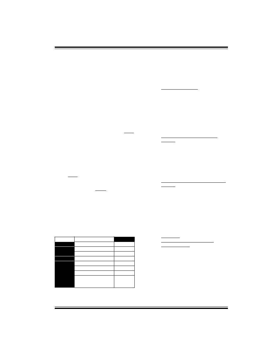
TABLE 1-1:
PIC16HV540 DEVICE
PIC16HV540
Clock
Maximum Frequency (MHz)
20
Memory
EPROM Program Memory
512
RAM Data Memory (bytes)
25
Peripherals
Timer Module(s)
TMR0
Packages
I/O Pins
12
Voltage Range (Volts)
3.5V-15V
Number of Instructions
33
Packages
18-pin DIP
SOIC
20-pin SSOP
All PICmicro
Æ
devices have Power-on Reset, selectable
WDT, selectable code protect and high I/O current capability.
2.0
PIC16HV540 DEVICE
VARIETIES
A variety of frequency ranges and packaging options
are available. When placing orders, please use the
PIC16HV540 Product Identification System at the back
of this data sheet to specify the correct part number.
2.1
UV Erasable Devices
The UV erasable versions, offered in CERDIP pack-
ages, are optimal for prototype development and pilot
programs.
UV erasable devices can be programmed for any of the
four oscillator configurations. Microchip's PICSTART
Æ
and PRO MATE
Æ
programmers both support program-
ming of the PIC16HV540. Third party programmers
also are available; refer to Literature Number DS00104
for a list of sources.
2.2
One-Time-Programmable (OTP)
Devices
The availability of OTP devices is especially useful for
customers expecting frequent code changes and
updates.
The OTP devices, packaged in plastic packages, per-
mit the user to program them once. In addition to the
program memory, the configuration bits must be pro-
grammed.
2.3
Quick-Turnaround-Production (QTP)
Devices
Microchip offers a QTP Programming Service for fac-
tory production orders. This service is made available
for users who choose not to program a medium to high
quantity of units and whose code patterns have stabi-
lized. The devices are identical to the OTP devices but
with all EPROM locations and configuration bit options
already programmed by the factory. Certain code and
prototype verification procedures apply before produc-
tion shipments are available. Please contact your
Microchip Technology sales office for more details.
2.4
Serialized
Quick-Turnaround-Production
(SQTP) Devices
Microchip offers the unique programming service where
a few user-defined locations in each device are pro-
grammed with different serial numbers. The serial num-
bers may be random, pseudo-random or sequential.
Serial programming allows each device to have a
unique number which can serve as an entry code,
password or ID number.
PIC16HV540
DS40197A-page 4
Preliminary
©
1998 Microchip Technology Inc.
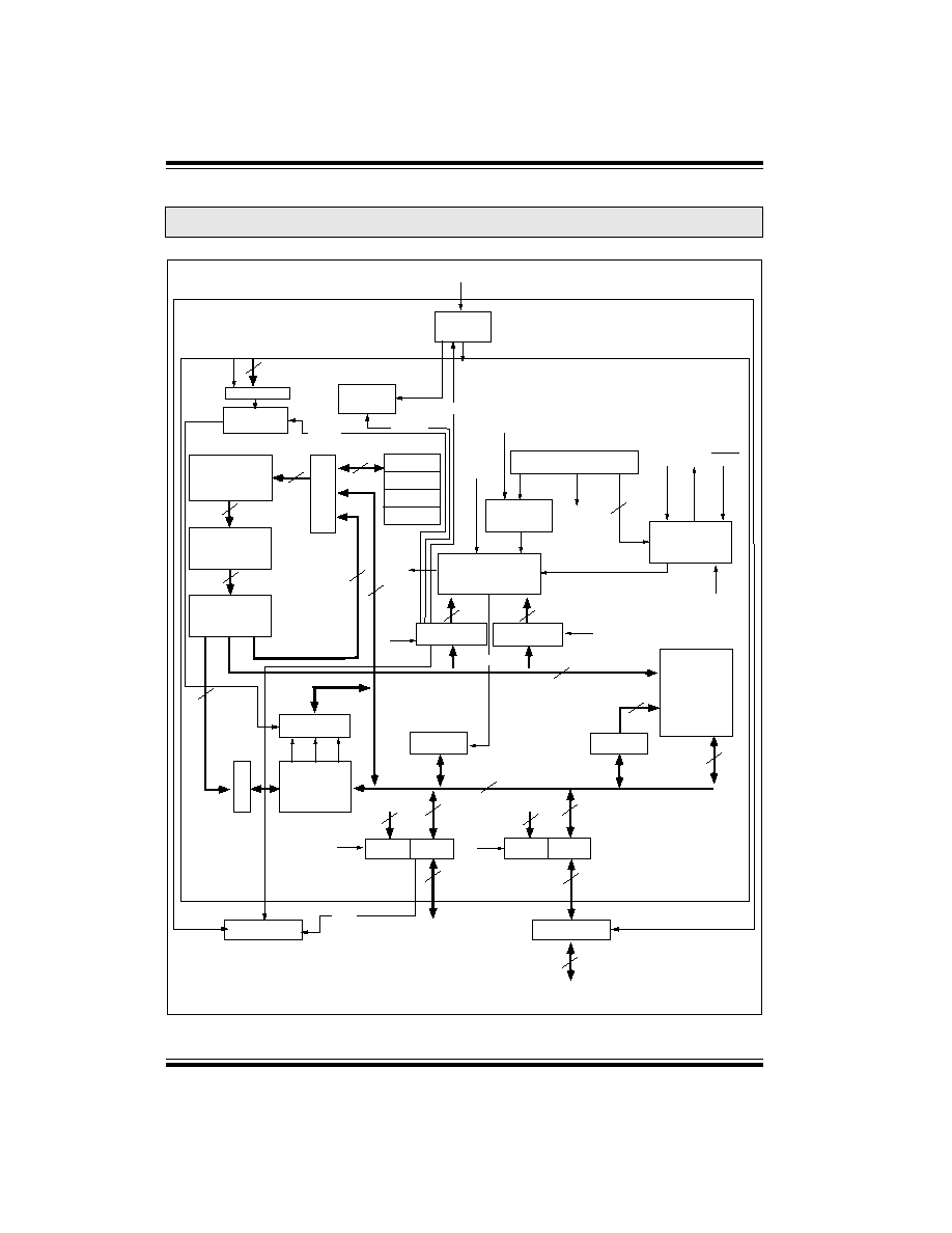
3.0
ARCHITECTURAL OVERVIEW
FIGURE 3-1:
PIC16HV540 BLOCK DIAGRAM
This section provides information on the architecture of the PIC16HV540. For information on operation of the periph-
erals, electrical specifications, etc., please refer to the PIC16C5X data sheet (DS30453).
WDT
TIME
OUT
8
STACK 1
EPROM
512 X 12
INSTRUCTION
REGISTER
INSTRUCTION
DECODER
WATCH-
DOG
CONFIGURATION WORD
OSCILLATOR/
TIMING &
CONTROL
GENERAL
PURPOSE
REGISTER
FILE
(SRAM)
25 Bytes
WDT/TMR0
PRESCALER
OPTION
"OPTION"
"SLEEP"
"CODE
PROTECT"
"OSC
SELECT"
DIRECT ADDRESS
TMR0
FROM W
FROM W
"TRIS 5"
"TRIS 6"
FSR
TRISA
PORTA
TRISB
PORT
T0CKI
PIN
9-11
9-11
12
12
8
W
4
4
4
DATA BUS
8
8
8
8
ALU
STATUS
FROM W
CLKOUT
8
9
6
5
5-7
OSC1 OSC2 MCLR
LITERALS
PC
"DISABLE"
2
RA3:RA0
RB7:RB0
DIRECT RAM
ADDRESS
8
HIGH VOLTAGE
TRANSLATION
V
REG
3V/5V
Regulator
VDD
STACK 2
STACK 3
STACK 4
"TRIS 7"
FROM W
6
OPTION2
3V/5V
Regulator
BOD
BL/BE
RL/SL
V
IO
PC
(PIN CHANGE)
WPC
4
RB3 : RB0
FILTER
RB7
SWE (OPTION2 REGISTER)

©
1998 Microchip Technology Inc.
Preliminary
DS40197A-page 5
PIC16HV540
TABLE 3-1:
PINOUT DESCRIPTION - PIC16HV540
Name
DIP, SOIC
No.
SSOP
No.
I/O/P
Type
Input
Levels
Description
RA0
RA1
RA2
RA3
17
18
1
2
19
20
1
2
I/O
I/O
I/O
I/O
TTL
TTL
TTL
TTL
Independently regulated Bi-directional I/O port -- V
IO
RB0
RB1
RB2
RB3
RB4
RB5
RB6
RB7
6
7
8
9
10
11
12
13
7
8
9
10
11
12
13
14
I/O
I/O
I/O
I/O
I/O
I/O
I/O
I/O
TTL
TTL
TTL
TTL
TTL
TTL
TTL
TTL
High-voltage Bi-directional I/O port.
Sourced from V
DD
.
T0CKI
3
3
I
ST
Clock input to Timer 0. Must be tied to V
SS
or V
DD,
if not in
use, to reduce current consumption.
MCLR/V
PP
4
4
I
ST
Master clear (reset) input/programming voltage input. This
pin is an active low reset to the device. Voltage on the
MCLR/V
PP
pin must not exceed V
DD
to avoid unintended
entering of programming mode.
OSC1/CLKIN
16
18
I
ST
Oscillator crystal input/external clock source input.
OSC2/CLKOUT
15
17
O
--
Oscillator crystal output. Connects to crystal or resonator in
crystal oscillator mode. In RC mode, OSC2 pin outputs
CLKOUT which has 1/4 the frequency of OSC1, and denotes
the instruction cycle rate.
V
DD
14
15,16
P
--
Positive supply.
V
SS
5
5,6
P
--
Ground reference.
Legend: I = input, O = output, I/O = input/output,
P = power, -- = Not Used, TTL = TTL input,
ST = Schmitt Trigger input
Wake up on
pin change.
Wake up on SLOW
rising pin change.