�
7/99 Microchip Technology Inc.
Preliminary
DS39026B-page 1
High Performance RISC CPU:
� C-compiler optimized architecture/instruction set
- Source code compatible with the PIC16CXX
instruction set
� Linear program memory addressing to 2M bytes
� Linear data memory addressing to 4K bytes
� Up to 10 MIPs operation:
- DC - 40 MHz osc./clock input
- 4 MHz - 10 MHz osc./clock input with PLL active
� 16-bit wide instructions, 8-bit wide data path
� Priority levels for interrupts
� 8 x 8 Single Cycle Hardware Multiplier
Peripheral Features:
� High current sink/source 25 mA/25 mA
� Three external interrupt pins
� Timer0 module: 8-bit/16-bit timer/counter with
8-bit programmable prescaler
� Timer1 module: 16-bit timer/counter
� Timer2 module: 8-bit timer/counter with 8-bit
period register (time-base for PWM)
� Timer3 module: 16-bit timer/counter
� Secondary oscillator clock option - Timer1/Timer3
� Two Capture/Compare/PWM (CCP) modules. CCP
pins that can be configured as:
- Capture input: capture is 16-bit,
max. resolution 6.25 ns (T
CY
/16)
- Compare is 16-bit, max. resolution 100 ns (T
CY
)
- PWM output: PWM resolution is 1- to 10-bit.
Max. PWM freq. @: 8-bit resolution = 156 kHz
10-bit resolution = 39 kHz
� Master Synchronous Serial Port (MSSP) module.
Two modes of operation:
- 3-wire SPITM (supports all 4 SPI modes)
- I
2
CTM master and slave mode
� Addressable USART module:
- Supports interrupt on Address bit
� Parallel Slave Port (PSP) module
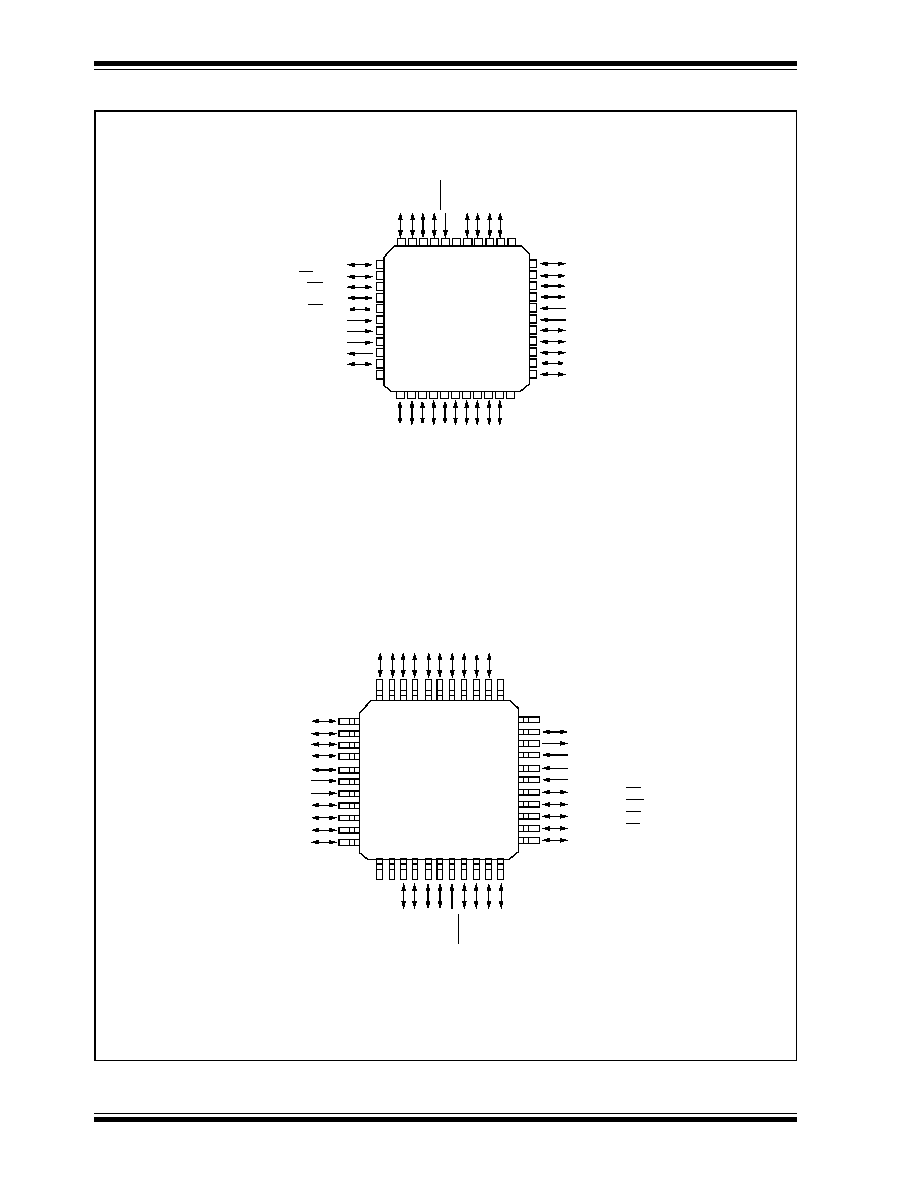
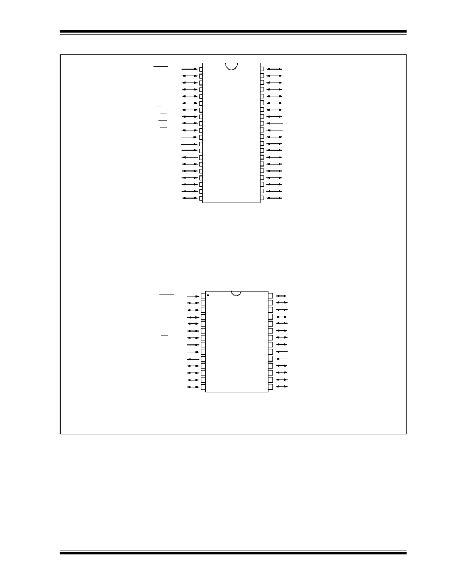
Pin Diagrams
Analog Features:
� 10-bit Analog-to-Digital Converter module (A/D)
with:
-
Fast sampling rate
-
Conversion available during sleep
-
DNL = �1 LSb, INL = �1 LSb
� Programmable Low-Voltage Detection (LVD)
module
-
Supports interrupt on low voltage detection
� Programmable Brown-out Reset (BOR)
Special Microcontroller Features:
� Power-on Reset (POR), Power-up Timer (PWRT)
and Oscillator Start-up Timer (OST)
� Watchdog Timer (WDT) with its own on-chip RC
oscillator for reliable operation
� Programmable code-protection
� Power saving SLEEP mode
� Selectable oscillator options including:
-
4X Phase Lock Loop (of primary oscillator)
-
Secondary Oscillator (32 kHz) clock input
� In-Circuit Serial Programming (ICSPTM) via two pins
CMOS Technology:
� Low-power, high-speed EPROM technology
� Fully static design
� Wide operating voltage range (2.5V to 5.5V)
� Industrial and Extended temperature ranges
� Low-power consumption
Device
On-Chip Program Memory On-Chip
RAM
(bytes)
EPROM
(bytes)
# Single Word
Instructions
PIC18C242
16K
8192
512
PIC18C252
32K
16384
1536
PIC18C442
16K
8192
512
PIC18C452
32K
16384
1536
*
*
*
*
*
RB7
RB6
RB5
RB4
RB3/CCP2
*
RB2/INT2
RB1/INT1
RB0/INT0
V
DD
V
SS
RD7/PSP7
RD6/PSP6
RD5/PSP5
RD4/PSP4
RC7/RX/DT
RC6/TX/CK
RC5/SDO
RC4/SDI/SDA
RD3/PSP3
RD2/PSP2
MCLR/V
PP
RA0/AN
0
RA1/AN1
RA2/AN2/V
REF
-
RA3/AN3/V
REF
+
RA4/T0CKI
RA5/AN4/SS/LVDIN
RE0/RD/AN5
RE1/WR/AN6
RE2/CS/AN7
V
DD
V
SS
OSC1/CLKI
OSC2/CLKO/RA6
RC0/T1OSO/T1CKI
RC1/T1OSI/CCP2
*
RC2/CCP1
RC3/SCK/SCL
RD0/PSP0
RD1/PSP1
1
2
3
4
5
6
7
8
9
10
11
12
13
14
15
16
17
18
19
20
40
39
38
37
36
35
34
33
32
31
30
29
28
27
26
25
24
23
22
21
PI
C
1
8C
4
X
2
*
RB3 is the alternate pin for the CCP2 pin multiplexing.
DIP, Windowed CERDIP
NOTE: Pin compatible with 40-pin PIC16C7X devices
PIC18CXX2
High-Performance Microcontrollers with 10-Bit A/D

DS39026B-page 4
Preliminary
�
7/99 Microchip Technology Inc.
PIC18CXX2
Table of Contents
1.0
Device Overview .......................................................................................................................................................................... 5
2.0
Oscillator Configurations ............................................................................................................................................................ 15
3.0
Reset .......................................................................................................................................................................................... 23
4.0
Memory Organization ................................................................................................................................................................. 33
5.0
Table Reads/Table Writes .......................................................................................................................................................... 53
6.0
8 X 8 Hardware Multiplier ........................................................................................................................................................... 61
7.0
Interrupts .................................................................................................................................................................................... 65
8.0
I/O Ports ..................................................................................................................................................................................... 77
9.0
Timer0 Module ........................................................................................................................................................................... 93
10.0 Timer1 Module ........................................................................................................................................................................... 97
11.0 Timer2 Module ......................................................................................................................................................................... 102
12.0 Timer3 Module ......................................................................................................................................................................... 105
13.0 Capture/Compare/PWM (CCP) Modules ................................................................................................................................. 109
14.0 Master Synchronous Serial Port (MSSP) Module .................................................................................................................... 117
15.0 Addressable Universal Synchronous Asynchronous Receiver Transmitter (USART).............................................................. 151
16.0 10-bit Analog-to-Digital Converter (A/D) Module ...................................................................................................................... 167
17.0 Low Voltage Detect .................................................................................................................................................................. 175
18.0 Special Features of the CPU .................................................................................................................................................... 181
19.0 Instruction Set Summary .......................................................................................................................................................... 191
20.0 Development Support............................................................................................................................................................... 235
21.0 Electrical Characteristics .......................................................................................................................................................... 241
22.0 DC and AC Characteristics Graphs and Tables ....................................................................................................................... 273
23.0 Packaging Information.............................................................................................................................................................. 275
Appendix A:
Revision History ......................................................................................................................................................... 283
Appendix B:
Device Differences..................................................................................................................................................... 283
Appendix C:
Conversion Considerations........................................................................................................................................ 284
Appendix D:
Migration from Baseline to Enhanced Devices .......................................................................................................... 284
Appendix E:
Migration from Midrange to Enhanced Devices ......................................................................................................... 285
Appendix F:
Migration from High-end to Enhanced Devices ......................................................................................................... 285
Index ................................................................................................................................................................................................. 287
On-Line Support................................................................................................................................................................................. 293
Reader Response .............................................................................................................................................................................. 294
PIC18CXX2 Product Identification System ........................................................................................................................................ 295
To Our Valued Customers
Most Current Data Sheet
To obtain the most up-to-date version of this data sheet, please register at our Worldwide Web site at:
http://www.microchip.com
You can determine the version of a data sheet by examining its literature number found on the bottom outside corner of any page.
The last character of the literature number is the version number. e.g., DS30000A is version A of document DS30000.
New Customer Notification System
Register on our web site (www.microchip.com/cn) to receive the most current information on our products.
Errata
An errata sheet may exist for current devices, describing minor operational differences (from the data sheet) and recommended
workarounds. As device/documentation issues become known to us, we will publish an errata sheet. The errata will specify the revi-
sion of silicon and revision of document to which it applies.
To determine if an errata sheet exists for a particular device, please check with one of the following:
� Microchip's Worldwide Web site; http://www.microchip.com
� Your local Microchip sales office (see last page)
� The Microchip Corporate Literature Center; U.S. FAX: (602) 786-7277
When contacting a sales office or the literature center, please specify which device, revision of silicon and data sheet (include liter-
ature number) you are using.
Corrections to this Data Sheet
We constantly strive to improve the quality of all our products and documentation. We have spent a great deal of time to ensure
that this document is correct. However, we realize that we may have missed a few things. If you find any information that is missing
or appears in error, please:
� Fill out and mail in the reader response form in the back of this data sheet.
� E-mail us at webmaster@microchip.com.
We appreciate your assistance in making this a better document.
�
7/99 Microchip Technology Inc.
Preliminary
DS39026B-page 5
PIC18CXX2
1.0
DEVICE OVERVIEW
This document contains device-specific information for
the following four devices:
1.
PIC18C242
2.
PIC18C252
3.
PIC18C442
4.
PIC18C452
These devices come in 28 and 40-pin packages. The
28-pin devices do not have a Parallel Slave Port (PSP)
implemented and the number of Analog-to-Digital (A/D)
converter input channels is reduced to 5. An overview
of features is shown in Table 1-1.
The following two figures are device block diagrams
sorted by pin count; 28-pin for Figure 1-1 and 40-pin for
Figure 1-2. The 28-pin and 40-pin pinouts are listed in
Table 1-2 and Table 1-3 respectively.
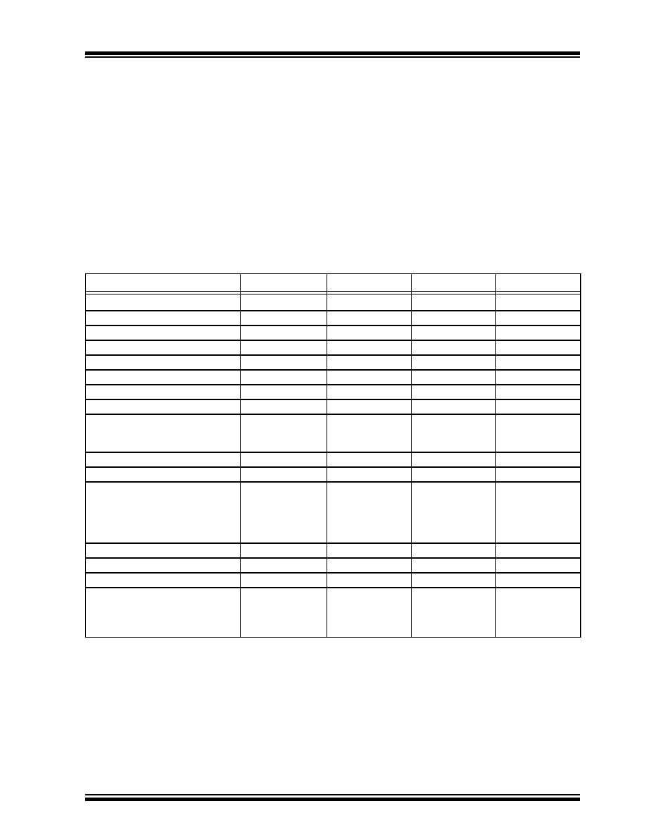
TABLE 1-1:
DEVICE FEATURES
Features
PIC18C242
PIC18C252
PIC18C442
PIC18C452
Operating Frequency
DC - 40 MHz
DC - 40 MHz
DC - 40 MHz
DC - 40 MHz
Program Memory (Bytes)
16K
32K
16K
32K
Program Memory (Instructions)
8192
16384
8192
16384
Data Memory (Bytes)
512
1536
512
1536
Interrupt sources
16
16
17
17
I/O Ports
Ports A, B, C
Ports A, B, C
Ports A, B, C, D, E Ports A, B, C, D, E
Timers
4
4
4
4
Capture/Compare/PWM modules
2
2
2
2
Serial Communications
MSSP,
Addressable
USART
MSSP,
Addressable
USART
MSSP,
Addressable
USART
MSSP,
Addressable
USART
Parallel Communications
--
--
PSP
PSP
10-bit Analog-to-Digital Module
5 input channels
5 input channels
8 input channels
8 input channels
Resets (and Delays)
POR, BOR,
Reset Instruction,
Stack Full,
Stack Underflow
(PWRT, OST)
POR, BOR,
Reset Instruction,
Stack Full,
Stack Underflow
(PWRT, OST)
POR, BOR,
Reset Instruction,
Stack Full,
Stack Underflow
(PWRT, OST)
POR, BOR,
Reset Instruction,
Stack Full,
Stack Underflow
(PWRT, OST)
Programmable Low Voltage Detect
Yes
Yes
Yes
Yes
Programmable Brown-out Reset
Yes
Yes
Yes
Yes
Instruction Set
75 Instructions
75 Instructions
75 Instructions
75 Instructions
Packages
28-pin DIP
28-pin SOIC
28-pin JW
28-pin DIP
28-pin SOIC
28-pin JW
40-pin DIP
40-pin PLCC
40-pin TQFP
40-pin JW
40-pin DIP
40-pin PLCC
40-pin TQFP
40-pin JW