DS39616B-page ii
Preliminary
2003 Microchip Technology Inc.
Information contained in this publication regarding device
applications and the like is intended through suggestion only
and may be superseded by updates. It is your responsibility to
ensure that your application meets with your specifications.
No representation or warranty is given and no liability is
assumed by Microchip Technology Incorporated with respect
to the accuracy or use of such information, or infringement of
patents or other intellectual property rights arising from such
use or otherwise. Use of Microchip's products as critical
components in life support systems is not authorized except
with express written approval by Microchip. No licenses are
conveyed, implicitly or otherwise, under any intellectual
property rights.
Trademarks
The Microchip name and logo, the Microchip logo, Accuron,
dsPIC, K
EE
L
OQ
, MPLAB, PIC, PICmicro, PICSTART,
PRO MATE and PowerSmart are registered trademarks of
Microchip Technology Incorporated in the U.S.A. and other
countries.
AmpLab, FilterLab, micro
ID
, MXDEV, MXLAB, PICMASTER,
SEEVAL, SmartShunt and The Embedded Control Solutions
Company are registered trademarks of Microchip Technology
Incorporated in the U.S.A.
Application Maestro, dsPICDEM, dsPICDEM.net,
dsPICworks, ECAN, ECONOMONITOR, FanSense,
FlexROM, fuzzyLAB, In-Circuit Serial Programming, ICSP,
ICEPIC, microPort, Migratable Memory, MPASM, MPLIB,
MPLINK, MPSIM, PICkit, PICDEM, PICDEM.net, PICtail,
PowerCal, PowerInfo, PowerMate, PowerTool, rfLAB, rfPIC,
Select Mode, SmartSensor, SmartTel and Total Endurance
are trademarks of Microchip Technology Incorporated in the
U.S.A. and other countries.
Serialized Quick Turn Programming (SQTP) is a service mark
of Microchip Technology Incorporated in the U.S.A.
All other trademarks mentioned herein are property of their
respective companies.
� 2003, Microchip Technology Incorporated, Printed in the
U.S.A., All Rights Reserved.
Printed on recycled paper.
Note the following details of the code protection feature on Microchip devices:
�
Microchip products meet the specification contained in their particular Microchip Data Sheet.
�
Microchip believes that its family of products is one of the most secure families of its kind on the market today, when used in the
intended manner and under normal conditions.
�
There are dishonest and possibly illegal methods used to breach the code protection feature. All of these methods, to our
knowledge, require using the Microchip products in a manner outside the operating specifications contained in Microchip's Data
Sheets. Most likely, the person doing so is engaged in theft of intellectual property.
�
Microchip is willing to work with the customer who is concerned about the integrity of their code.
�
Neither Microchip nor any other semiconductor manufacturer can guarantee the security of their code. Code protection does not
mean that we are guaranteeing the product as "unbreakable."
Code protection is constantly evolving. We at Microchip are committed to continuously improving the code protection features of our
products. Attempts to break microchip's code protection feature may be a violation of the Digital Millennium Copyright Act. If such acts
allow unauthorized access to your software or other copyrighted work, you may have a right to sue for relief under that Act.
Microchip received ISO/TS-16949:2002 quality system certification for
its worldwide headquarters, design and wafer fabrication facilities in
Chandler and Tempe, Arizona and Mountain View, California in October
2003 . The Company's quality system processes and procedures are
for its PICmicro
�
8-bit MCUs, K
EE
L
OQ
�
code hopping devices, Serial
EEPROMs, microperipherals, non-volatile memory and analog
products. In addition, Microchip's quality system for the design and
manufacture of development systems is ISO 9001:2000 certified.
2003 Microchip Technology Inc.
Preliminary
DS39616B-page 1
14-bit Power Control PWM Module:
� Up to 4 channels with complementary outputs
� Edge- or center-aligned operation
� Flexible dead-band generator
� Hardware fault protection inputs
� Simultaneous update of duty cycle and period:
- Flexible special event trigger output
Motion Feedback Module:
� Three independent input capture channels:
- Flexible operating modes for period and pulse
width measurement
- Special Hall Sensor interface module
- Special event trigger output to other modules
� Quadrature Encoder Interface:
- 2 phase inputs and one index input from encoder
- High and low position tracking with direction
status and change of direction interrupt
- Velocity measurement
High-Speed, 200 Ksps 10-bit A/D Converter:
� Up to 9 channels
� Simultaneous two-channel sampling
� Sequential sampling: 1, 2 or 4 selected channels
� Auto-conversion capability
� 4-word FIFO with selectable interrupt frequency
� Selectable external conversion triggers
� Programmable acquisition time
Flexible Oscillator Structure:
� Four crystal modes up to 40 MHz
� Two external clock modes up to 40 MHz
� Internal oscillator block:
- 8 user selectable frequencies: 31 kHz to 8 MHz
- OSCTUNE can compensate for frequency drift
� Secondary oscillator using Timer1 @ 32 kHz
� Fail-Safe Clock Monitor:
- Allows for safe shutdown of device if clock fails
Power-Managed Modes:
� Run
CPU on, peripherals on
� Idle
CPU off, peripherals on
� Sleep
CPU off, peripherals off
� Idle mode currents down to 5.8
�
A typical
� Sleep current down to 0.1
�
A typical
� Timer1 oscillator, 1.8
�
A typical, 32 kHz, 2V
� Watchdog Timer (WDT), 2.1
�
A typical
� Two-Speed oscillator start-up
Peripheral Highlights:
� High current sink/source 25 mA/25 mA
� Three external interrupts
� Two Capture/Compare/PWM (CCP) modules:
- Capture is 16-bit, max. resolution 6.25 ns (T
CY
/16)
- Compare is 16-bit, max. resolution 100 ns (T
CY
)
- PWM output: PWM resolution is 1 to 10 bits
� Enhanced USART module:
- Supports RS-485, RS-232 and LIN 1.2
- Auto-Wake-up on Start bit
- Auto-Baud detect
� RS-232 operation using internal oscillator block
(no external crystal required)
Special Microcontroller Features:
� 100,000 erase/write cycle enhanced Flash
program memory typical
� 1,000,000 erase/write cycle data EEPROM
memory typical
� Flash/data EEPROM retention: 100 years
� Self-programmable under software control
� Priority levels for interrupts
� 8 X 8 Single-cycle Hardware Multiplier
� Extended Watchdog Timer (WDT):
- Programmable period from 41 ms to 131s
� Single-supply In-Circuit Serial ProgrammingTM
(ICSPTM) via two pins
� In-Circuit Debug (ICD) via two pins
- Drives PWM outputs safely when debugging
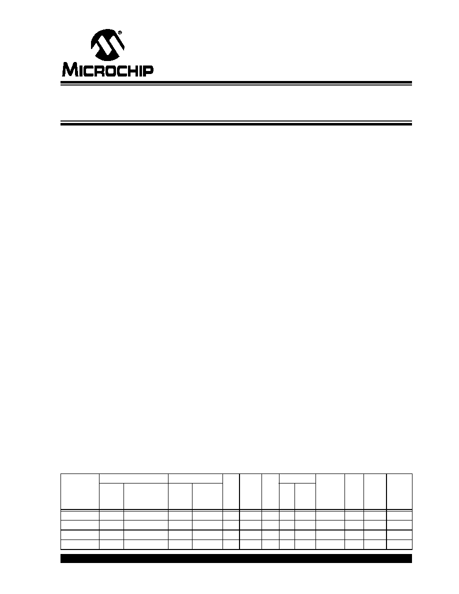
Device
Program Memory
Data Memory
I/O
10-bit
A/D
(ch)
CCP
SSP
EUSART
Qu
a
d
r
a
t
u
re
E
n
c
ode
r
14-bit
PWM
(ch)
Timers
8/16-bit
Flash
(bytes)
# Single-Word
Instructions
SRAM
(bytes)
EEPROM
(bytes)
SPI
Slave
I
2
CTM
PIC18F2331
8192
4096
768
256
24
5
2
Y
Y
Y
Y
6
1/3
PIC18F2431
16384
8192
768
256
24
5
2
Y
Y
Y
Y
6
1/3
PIC18F4331
8192
4096
768
256
36
9
2
Y
Y
Y
Y
8
1/3
PIC18F4431
16384
8192
768
256
36
9
2
Y
Y
Y
Y
8
1/3
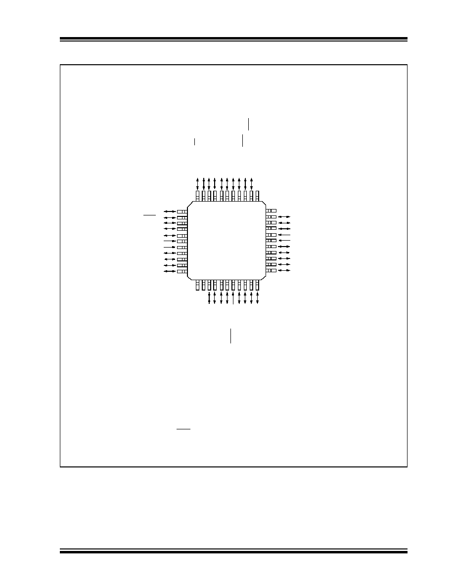
28/40/44-Pin Enhanced Flash Microcontrollers with
nanoWatt Technology, High Performance PWM and A/D
PIC18F2331/2431/4331/4431
PIC18F2331/2431/4331/4431
DS39616B-page 2
Preliminary
2003 Microchip Technology Inc.
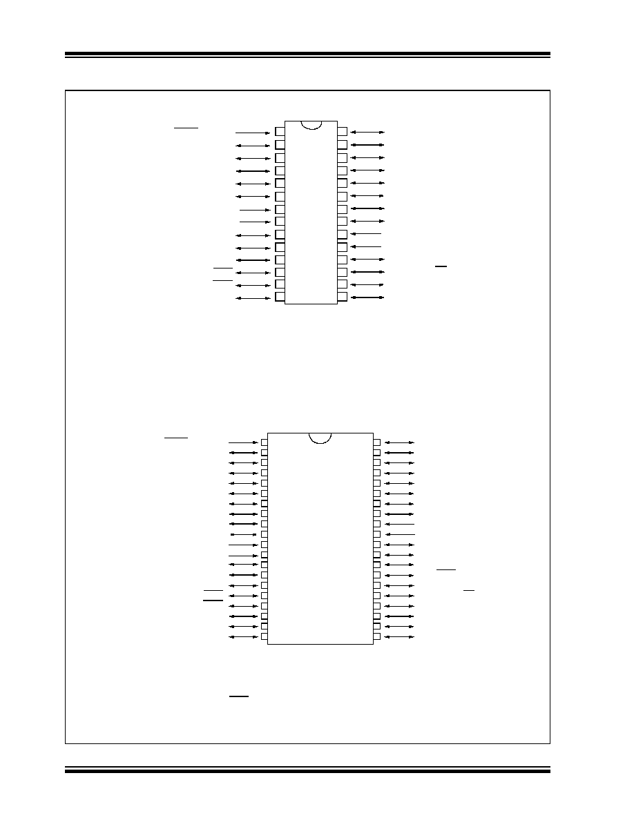
Pin Diagrams
40-Pin PDIP
28-Pin SDIP, SOIC
MCLR/V
PP
/RE3
RA0/AN0
RA1/AN1
RA2/AN2/V
REF
-/CAP1/INDX
RA3/AN3/V
REF
+/CAP2/QEA
RA4/AN4/CAP3/QEB
AV
DD
AV
SS
OSC1/CLKI/RA7
OSC2/CLKO/RA6
RC0/T1OSO/T1CKI
RC1/T1OSI/CCP2/FLTA
RC2/CCP1/FLTB
RC3/T0CKI/T5CKI/INT0
RB7/KBI3/PGD
RB6/KBI2/PGC
RB5/KBI1/PWM4/PGM
(1)
RB4/KBI0/PWM5
RB3/PWM3
RB2/PWM2
RB1/PWM1
RB0/PWM0
V
DD
V
SS
RC7/RX/DT/SDO
RC6/TX/CK/SS
RC5/INT2/SCK/SCL
RC4/INT1/SDI/SDA
� 1
2
3
4
5
6
7
8
9
10
11
12
13
14
28
27
26
25
24
23
22
21
20
19
18
17
16
15
PIC
1
8
F
233
1/2
431
Note 1:
Low-voltage programming must be enabled.
RB7/KBI3/PGD
RB6/KBI2/PGC
RB5/KBI1/PWM4/PGM
(2)
RB4/KBI0/PWM5
RB3/PWM3
RB2/PWM2
RB1/PWM1
RB0/PWM0
V
DD
V
SS
RD7/PWM7
RD6/PWM6
RD5/PWM4
(4)
RD4/FLTA
(3)
RC7/RX/DT/SDO
(1)
RC6/TX/CK/SS
RC5/INT2/SCK
(1)
/SCL
(1)
RC4/INT1/SDI
(1)
/SDA
(1)
RD3/SCK/SCL
RD2/SDI/SDA
MCLR/V
PP
/RE3
RA0/AN0
RA1/AN1
RA2/AN2/V
REF
-/CAP1/INDX
RA3/AN3/V
REF
+/CAP2/QEA
RA4/AN4/CAP3/QEB
RA5/AN5/LVDIN
RE0/AN6
RE1/AN7
RE2/AN8
AV
DD
AV
SS
OSC1/CLKI/RA7
OSC2/CLKO/RA6
RC0/T1OSO/T1CKI
RC1/T1OSI/CCP2/FLTA
RC2/CCP1/FLTB
RC3/T0CKI
(1)
/T5CKI
(1)
/INT0
RD0/T0CKI/T5CKI
RD1/SDO
1
2
3
4
5
6
7
8
9
10
11
12
13
14
15
16
17
18
19
20
40
39
38
37
36
35
34
33
32
31
30
29
28
27
26
25
24
23
22
21
PIC
1
8
F
43
31/
443
1
Note 1:
RC3 is the alternate pin for T0CKI/T5CKI; RC4 is the alternate pin for SDI/SDA; RC5 is the alternate pin
for SCK/SCL.
2:
Low-voltage programming must be enabled.
3:
RD4 is the alternate pin for FLTA.
4:
RD5 is the alternate pin for PWM4.