
� 2006 Microchip Technology Inc.
Advance Information
DS39760A
PIC18F2450/4450
Data Sheet
28/40/44-Pin, High-Performance,
12 MIPS, Enhanced Flash,
USB Microcontrollers with
nanoWatt Technology

DS39760A-page ii
Advance Information
� 2006 Microchip Technology Inc.
Information contained in this publication regarding device
applications and the like is provided only for your convenience
and may be superseded by updates. It is your responsibility to
ensure that your application meets with your specifications.
MICROCHIP MAKES NO REPRESENTATIONS OR WAR-
RANTIES OF ANY KIND WHETHER EXPRESS OR IMPLIED,
WRITTEN OR ORAL, STATUTORY OR OTHERWISE,
RELATED TO THE INFORMATION, INCLUDING BUT NOT
LIMITED TO ITS CONDITION, QUALITY, PERFORMANCE,
MERCHANTABILITY OR FITNESS FOR PURPOSE.
Microchip disclaims all liability arising from this information and
its use. Use of Microchip's products as critical components in
life support systems is not authorized except with express
written approval by Microchip. No licenses are conveyed,
implicitly or otherwise, under any Microchip intellectual property
rights.
Trademarks
The Microchip name and logo, the Microchip logo, Accuron,
dsPIC, K
EE
L
OQ
, microID, MPLAB, PIC, PICmicro, PICSTART,
PRO MATE, PowerSmart, rfPIC, and SmartShunt are
registered trademarks of Microchip Technology Incorporated
in the U.S.A. and other countries.
AmpLab, FilterLab, Migratable Memory, MXDEV, MXLAB,
PICMASTER, SEEVAL, SmartSensor and The Embedded
Control Solutions Company are registered trademarks of
Microchip Technology Incorporated in the U.S.A.
Analog-for-the-Digital Age, Application Maestro, dsPICDEM,
dsPICDEM.net, dsPICworks, ECAN, ECONOMONITOR,
FanSense, FlexROM, fuzzyLAB, In-Circuit Serial
Programming, ICSP, ICEPIC, Linear Active Thermistor,
MPASM, MPLIB, MPLINK, MPSIM, PICkit, PICDEM,
PICDEM.net, PICLAB, PICtail, PowerCal, PowerInfo,
PowerMate, PowerTool, Real ICE, rfLAB, rfPICDEM, Select
Mode, Smart Serial, SmartTel, Total Endurance, UNI/O,
WiperLock and Zena are trademarks of Microchip Technology
Incorporated in the U.S.A. and other countries.
SQTP is a service mark of Microchip Technology Incorporated
in the U.S.A.
All other trademarks mentioned herein are property of their
respective companies.
� 2006, Microchip Technology Incorporated, Printed in the
U.S.A., All Rights Reserved.
Printed on recycled paper.
Note the following details of the code protection feature on Microchip devices:
�
Microchip products meet the specification contained in their particular Microchip Data Sheet.
�
Microchip believes that its family of products is one of the most secure families of its kind on the market today, when used in the
intended manner and under normal conditions.
�
There are dishonest and possibly illegal methods used to breach the code protection feature. All of these methods, to our
knowledge, require using the Microchip products in a manner outside the operating specifications contained in Microchip's Data
Sheets. Most likely, the person doing so is engaged in theft of intellectual property.
�
Microchip is willing to work with the customer who is concerned about the integrity of their code.
�
Neither Microchip nor any other semiconductor manufacturer can guarantee the security of their code. Code protection does not
mean that we are guaranteeing the product as "unbreakable."
Code protection is constantly evolving. We at Microchip are committed to continuously improving the code protection features of our
products. Attempts to break Microchip's code protection feature may be a violation of the Digital Millennium Copyright Act. If such acts
allow unauthorized access to your software or other copyrighted work, you may have a right to sue for relief under that Act.
Microchip received ISO/TS-16949:2002 quality system certification for
its worldwide headquarters, design and wafer fabrication facilities in
Chandler and Tempe, Arizona and Mountain View, California in
October 2003. The Company's quality system processes and
procedures are for its PICmicro
�
8-bit MCUs, K
EE
L
OQ
�
code hopping
devices, Serial EEPROMs, microperipherals, nonvolatile memory and
analog products. In addition, Microchip's quality system for the design
and manufacture of development systems is ISO 9001:2000 certified.

� 2006 Microchip Technology Inc.
Advance Information
DS39760A-page 1
Universal Serial Bus Features:
� USB V2.0 Compliant
� Low speed (1.5 Mb/s) and full speed (12 Mb/s)
� Supports control, interrupt, isochronous and
bulk transfers
� Supports up to 32 endpoints (16 bidirectional)
� 256-byte dual access RAM for USB
� On-chip USB transceiver with on-chip voltage
regulator
� Interface for off-chip USB transceiver
Power-Managed Modes:
� Run: CPU on, peripherals on
� Idle: CPU off, peripherals on
� Sleep: CPU off, peripherals off
� Idle mode currents down to 5.8
A typical
� Sleep mode currents down to 0.1
A typical
� Timer1 oscillator: 1.8
A typical, 32 kHz, 2V
� Watchdog Timer: 2.1
A typical
� Two-Speed Oscillator Start-up
Flexible Oscillator Structure:
� Four Crystal modes, including High-Precision PLL
for USB
� Two External Clock modes, up to 48 MHz
� Internal 31 kHz oscillator
� Secondary oscillator using Timer1 @ 32 kHz
� Dual oscillator options allow microcontroller and
USB module to run at different clock speeds
� Fail-Safe Clock Monitor:
- Allows for safe shutdown if any clock stops
Peripheral Highlights:
� High-current sink/source: 25 mA/25 mA
� Three external interrupts
� Three Timer modules (Timer0 to Timer2)
� Capture/Compare/PWM (CCP) module:
- Capture is 16-bit, max. resolution 5.2 ns
- Compare is 16-bit, max. resolution 83.3 ns
- PWM output: PWM resolution is 1 to 10-bit
� Enhanced USART module:
- LIN bus support
� 10-bit, up to 13-channel Analog-to-Digital Converter
module (A/D):
- Up to 100 ksps sampling rate
- Programmable acquisition time
Special Microcontroller Features:
� C compiler optimized architecture with optional
extended instruction set
� Flash memory retention: > 40 years
� Self-programmable under software control
� Priority levels for interrupts
� 8 x 8 Single-Cycle Hardware Multiplier
� Extended Watchdog Timer (WDT):
- Programmable period from 4 ms to 131s
� Programmable Code Protection
� Single-Supply In-Circuit Serial ProgrammingTM
(ICSPTM) via two pins
� In-Circuit Debug (ICD) via two pins
� Optional dedicated ICD/ICSP port
(44-pin TQFP devices only)
� Wide operating voltage range (2.0V to 5.5V)
Device
Program Memory
Data
Memory
SRAM
(bytes)
I/O
10-Bit A/D
(ch)
CCP
EUSART
Timers
8/16-Bit
Flash
(bytes)
# Single-Word
Instructions
PIC18F2450
16K
8192
768*
23
10
1
1
1/2
PIC18F4450
16K
8192
768*
34
13
1
1
1/2
*
Includes 256 bytes of dual access RAM used by USB module and shared with data memory.
28/40/44-Pin, High-Performance, 12 MIPS, Enhanced Flash,
USB Microcontrollers with nanoWatt Technology
PIC18F2450/4450
PIC18F2450/4450
DS39760A-page 2
Advance Information
� 2006 Microchip Technology Inc.
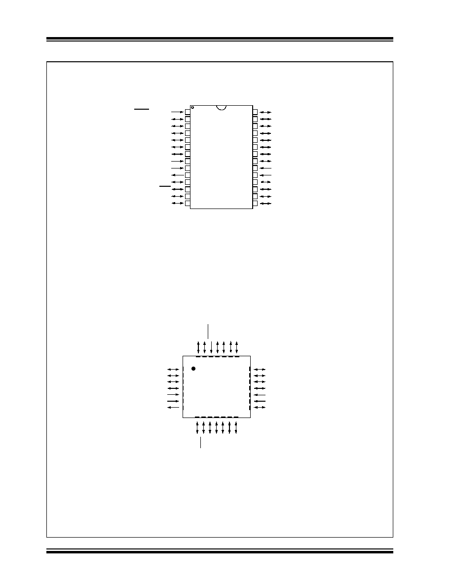
Pin Diagrams
28-Pin QFN
10
11
2
3
4
5
6
1
8
7
9
12
13
14
15
16
17
18
19
20
23
24
25
26
27
28
22
21
MCLR/V
PP
/RE3
RA0/AN0
RA1/AN1
RA2/AN2/V
REF
-
RA3/AN3/V
REF
+
RA4/T0CKI/RCV
RA5/AN4/HLVDIN
V
SS
OSC1/CLKI
OSC2/CLKO/RA6
RC0/T1OSO/T1CKI
RC1/T1OSI/UOE
RC2/CCP1
V
USB
RB7/KBI3/PGD
RB6/KBI2/PGC
RB5/KBI1/PGM
RB4/AN11/KBI0
RB3/AN9/VPO
RB2/AN8/INT2/VMO
RB1/AN10/INT1
RB0/AN12/INT0
V
DD
V
SS
RC7/RX/DT
RC6/TX/CK
RC5/D+/VP
RC4/D-/VM
28-Pin SDIP, SOIC
PI
C
1
8F2
450
Note:
Pinouts are subject to change.
10 11
2
3
6
1
18
19
20
21
22
12 13 14
15
8
7
16
17
23
24
25
26
27
28
9
PIC18F2450
RC0
/
T
1
O
SO/T
1
C
KI
5
4
RB7
/
KBI
3
/
PG
D
RB6
/
KBI
2
/
PG
C
RB5
/
KBI
1
/
PG
M
RB4
/
AN1
1
/
KBI
0
RB3/AN9/VPO
RB2/AN8/INT2/VMO
RB1/AN10/INT1
RB0/AN12/INT0
V
DD
V
SS
RC7/RX/DT
RC6
/T
X/C
K
RC5
/D+/
VP
RC4
/D-
/
VM
MC
L
R
/V
PP
/RE
3
RA0
/
AN0
RA1
/
AN1
RA2/AN2/V
REF
-
RA3/AN3/V
REF
+
RA4/T0CKI/RCV
RA5/AN4/HLVDIN
V
SS
OSC1/CLKI
OSC2/CLKO/RA6
R
C
1
/T
1O
S
I
/
U
OE
RC2
/CCP1
V
US
B
PIC18F2450/4450
� 2006 Microchip Technology Inc.
Advance Information
DS39760A-page 3
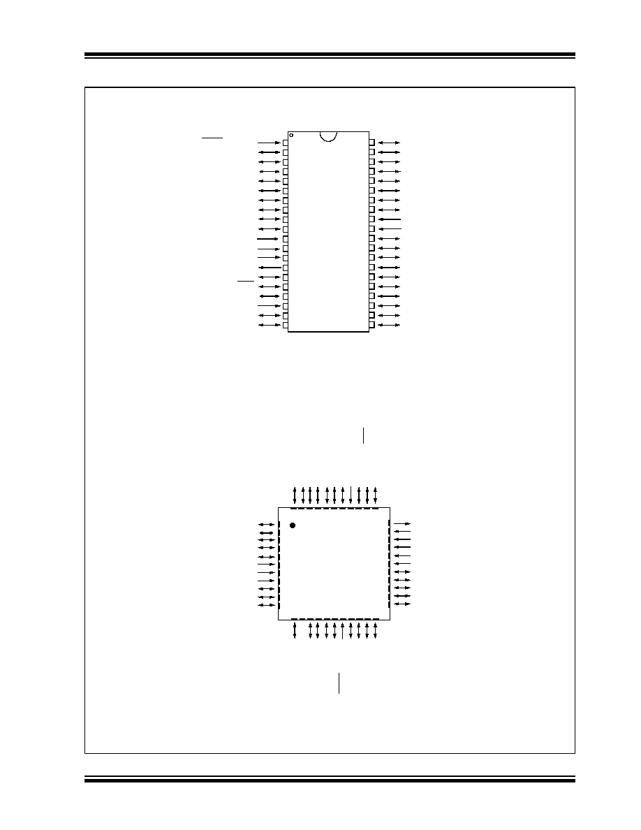
Pin Diagrams (Continued)
44-Pin QFN
10
11
2
3
6
1
18
19
20
21
22
12
13
14
15
38
8
7
44
43
42
41
40
39
16
17
29
30
31
32
33
23
24
25
26
27
28
36
34
35
9
37
RA3
/
AN3
/
V
RE
F
+
RA
2
/
AN2
/
V
RE
F
-
RA1
/
AN1
RA0
/
AN0
MC
L
R
/V
PP
/R
E
3
R
B
7/K
B
I
3/
P
G
D
R
B
6/K
B
I
2/
P
G
C
RB
5/
K
B
I1
/P
GM
NC
RC6
/T
X/CK
RC5
/D+/VP
RC4
/D-
/
VM
RD3
RD2
RD1
RD0
V
US
B
RC2
/CCP1
RC1/T
1O
S
I
/UOE
RC0/T
1O
S
O
/T
1
C
K
I
OSC2/CLKO/RA6
OSC1/CLKI
V
SS
AV
DD
RA5/AN4/HLVDIN
RA4/T0CKI/RCV
RC7/RX/DT
RD4
RD5
RD6
V
SS
V
DD
RB0/AN12/INT0
RB1/AN10/INT1
RB2/AN8/INT2/VMO
RB3
/
AN9
/
VP
O
RD7
5
4
AV
SS
V
DD
AV
DD
Note:
Pinouts are subject to change.
PIC18F4450
R
B
4
/
AN1
1
/
KBI
0
RE0/AN5
RE1/AN6
RE2/AN7
40-Pin PDIP
RB7/KBI3/PGD
RB6/KBI2/PGC
RB5/KBI1/PGM
RB4/AN11/KBI0
RB3/AN9/VPO
RB2/AN8/INT2/VMO
RB1/AN10/INT1
RB0/AN12/INT0
V
DD
V
SS
RD7
RD6
RD5
RD4
RC7/RX/DT
RC6/TX/CK
RC5/D+/VP
RC4/D-/VM
RD3
RD2
MCLR/V
PP
/RE3
RA0/AN0
RA1/AN1
RA2/AN2/V
REF
-
RA3/AN3/V
REF
+
RA4/T0CKI/RCV
RA5/AN4/HLVDIN
RE0/AN5
RE1/AN6
RE2/AN7
V
DD
V
SS
OSC1/CLKI
OSC2/CLKO/RA6
RC0/T1OSO/T1CKI
RC1/T1OSI/UOE
RC2/CCP1
V
USB
RD0
RD1
1
2
3
4
5
6
7
8
9
10
11
12
13
14
15
16
17
18
19
20
40
39
38
37
36
35
34
33
32
31
30
29
28
27
26
25
24
23
22
21
PIC
1
8F4
450
PIC18F2450/4450
DS39760A-page 4
Advance Information
� 2006 Microchip Technology Inc.
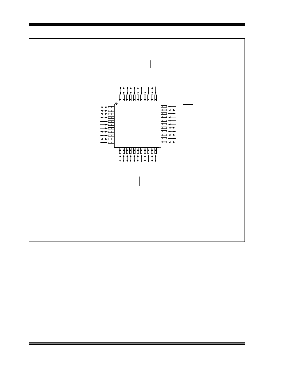
Pin Diagrams (Continued)
10
11
2
3
6
1
18
19
20
21
22
12
13
14
15
38
8
7
44
43
42
41
40
39
16
17
29
30
31
32
33
23
24
25
26
27
28
36
34
35
9
37
RA3
/
AN3
/
V
RE
F
+
RA1
/
AN1
MC
L
R
/V
PP
/RE
3
RC6
/T
X/CK
RC0/T1OSO/T1CKI
OSC2/CLKO/RA6
OSC1/CLKI
V
SS
V
DD
RA5/AN4/HLVDIN
RA4/T0CKI/RCV
V
SS
V
DD
44-Pin TQFP
5
4
PIC18F4450
RC7/RX/DT
RD4
RD5
RD6
RD7
RB0/AN12/INT0
RB1/AN10/INT1
RB2/AN8/INT2/VMO
RB3/AN9/VPO
RC1
/T
1
O
S
I/UO
E
RC2
/CCP1
V
US
B
RD0
RD1
RD2
RD3
RC4
/D-
/
VM
RC5
/D+/VP
RB
5/
K
B
I1
/P
GM
RB
6
/
KBI
2
/
PG
C
RB
7
/
KBI
3
/
PG
D
RA0
/
AN0
RA2
/
AN2
/
V
RE
F
-
Note:
Pinouts are subject to change.
*
Assignment of this feature is dependent on device configuration.
RB4
/
AN1
1
/
KBI
0
RE0/AN5
RE1/AN6
RE2/AN7
NC/
ICCK*
/
ICPGC*
NC/ICDT
*
/
ICPGD*
NC/ICRST*/ICV
PP
*
NC/I
C
P
O
R
T
S*

PIC18F2450/4450
� 2006 Microchip Technology Inc.
Advance Information
DS39760A-page 5
Table of Contents
1.0
Device Overview .......................................................................................................................................................................... 7
2.0
Oscillator Configurations ............................................................................................................................................................ 23
3.0
Power-Managed Modes ............................................................................................................................................................. 33
4.0
Reset .......................................................................................................................................................................................... 41
5.0
Memory Organization ................................................................................................................................................................. 53
6.0
Flash Program Memory.............................................................................................................................................................. 73
7.0
8 x 8 Hardware Multiplier............................................................................................................................................................ 83
8.0
Interrupts .................................................................................................................................................................................... 85
9.0
I/O Ports ..................................................................................................................................................................................... 99
10.0 Timer0 Module ......................................................................................................................................................................... 111
11.0 Timer1 Module ......................................................................................................................................................................... 115
12.0 Timer2 Module ......................................................................................................................................................................... 121
13.0 Capture/Compare/PWM (CCP) Module ................................................................................................................................... 123
14.0 Universal Serial Bus (USB) ...................................................................................................................................................... 129
15.0 Enhanced Universal Synchronous Receiver Transmitter (EUSART)....................................................................................... 153
16.0 10-Bit Analog-to-Digital Converter (A/D) Module ..................................................................................................................... 173
17.0 High/Low-Voltage Detect (HLVD)............................................................................................................................................. 183
18.0 Special Features of the CPU.................................................................................................................................................... 189
19.0 Instruction Set Summary .......................................................................................................................................................... 211
20.0 Development Support............................................................................................................................................................... 261
21.0 Electrical Characteristics .......................................................................................................................................................... 265
22.0 DC and AC Characteristics Graphs and Tables....................................................................................................................... 293
23.0 Packaging Information.............................................................................................................................................................. 295
Appendix A: Revision History............................................................................................................................................................. 303
Appendix B: Device Differences ........................................................................................................................................................ 303
Appendix C: Conversion Considerations ........................................................................................................................................... 304
Appendix D: Migration From Baseline to Enhanced Devices ............................................................................................................ 304
Appendix E: Migration From Mid-Range to Enhanced Devices ......................................................................................................... 305
Appendix F: Migration From High-End to Enhanced Devices............................................................................................................ 305
Index ................................................................................................................................................................................................. 307
The Microchip Web Site ..................................................................................................................................................................... 315
Customer Change Notification Service .............................................................................................................................................. 315
Customer Support .............................................................................................................................................................................. 315
Reader Response .............................................................................................................................................................................. 316
PIC18F2450/4450 Product Identification System .............................................................................................................................. 317

PIC18F2450/4450
DS39760A-page 6
Advance Information
� 2006 Microchip Technology Inc.
TO OUR VALUED CUSTOMERS
It is our intention to provide our valued customers with the best documentation possible to ensure successful use of your Microchip
products. To this end, we will continue to improve our publications to better suit your needs. Our publications will be refined and
enhanced as new volumes and updates are introduced.
If you have any questions or comments regarding this publication, please contact the Marketing Communications Department via
E-mail at docerrors@microchip.com or fax the Reader Response Form in the back of this data sheet to (480) 792-4150. We
welcome your feedback.
Most Current Data Sheet
To obtain the most up-to-date version of this data sheet, please register at our Worldwide Web site at:
http://www.microchip.com
You can determine the version of a data sheet by examining its literature number found on the bottom outside corner of any page.
The last character of the literature number is the version number, (e.g., DS30000A is version A of document DS30000).
Errata
An errata sheet, describing minor operational differences from the data sheet and recommended workarounds, may exist for current
devices. As device/documentation issues become known to us, we will publish an errata sheet. The errata will specify the revision
of silicon and revision of document to which it applies.
To determine if an errata sheet exists for a particular device, please check with one of the following:
� Microchip's Worldwide Web site; http://www.microchip.com
� Your local Microchip sales office (see last page)
When contacting a sales office, please specify which device, revision of silicon and data sheet (include literature number) you are
using.
Customer Notification System
Register on our web site at www.microchip.com to receive the most current information on all of our products.

PIC18F2450/4450
� 2006 Microchip Technology Inc.
Advance Information
DS39760A-page 7
1.0
DEVICE OVERVIEW
This document contains device-specific information for
the following devices:
This family of devices offers the advantages of all PIC18
microcontrollers � namely, high computational
performance at an economical price � with the addition of
high endurance, Enhanced Flash program memory. In
addition to these features, the PIC18F2450/4450 family
introduces design enhancements that make these micro-
controllers a logical choice for many high-performance,
power sensitive applications.
1.1
New Core Features
1.1.1
nanoWatt TECHNOLOGY
All of the devices in the PIC18F2450/4450 family
incorporate a range of features that can significantly
reduce power consumption during operation. Key
items include:
� Alternate Run Modes: By clocking the controller
from the Timer1 source or the internal RC
oscillator, power consumption during code
execution can be reduced by as much as 90%.
� Multiple Idle Modes: The controller can also run
with its CPU core disabled but the peripherals still
active. In these states, power consumption can be
reduced even further, to as little as 4% of normal
operation requirements.
� On-the-Fly Mode Switching: The power-
managed modes are invoked by user code during
operation, allowing the user to incorporate power-
saving ideas into their application's software
design.
� Low Consumption in Key Modules: The
power requirements for both Timer1 and the
Watchdog Timer are minimized. See
Section 21.0 "Electrical Characteristics" for
values.
1.1.2
UNIVERSAL SERIAL BUS (USB)
Devices in the PIC18F2450/4450 family incorporate a
fully featured Universal Serial Bus communications
module that is compliant with the USB Specification
Revision 2.0. The module supports both low-speed and
full-speed communication for all supported data
transfer types. It also incorporates its own on-chip
transceiver and 3.3V regulator and supports the use of
external transceivers and voltage regulators.
1.1.3
MULTIPLE OSCILLATOR OPTIONS
AND FEATURES
All of the devices in the PIC18F2450/4450 family offer
twelve different oscillator options, allowing users a wide
range of choices in developing application hardware.
These include:
� Four Crystal modes using crystals or ceramic
resonators.
� Four External Clock modes, offering the option of
using two pins (oscillator input and a divide-by-4
clock output) or one pin (oscillator input, with the
second pin reassigned as general I/O).
� An INTRC source (approximately 31 kHz, stable
over temperature and V
DD
). This option frees an
oscillator pin for use as an additional general
purpose I/O.
� A Phase Lock Loop (PLL) frequency multiplier,
available to both the High-Speed Crystal and
External Oscillator modes, which allows a wide
range of clock speeds from 4 MHz to 48 MHz.
� Asynchronous dual clock operation, allowing the
USB module to run from a high-frequency
oscillator while the rest of the microcontroller is
clocked from an internal low-power oscillator.
The internal oscillator provides a stable reference
source that gives the family additional features for
robust operation:
� Fail-Safe Clock Monitor: This option constantly
monitors the main clock source against a
reference signal provided by the internal
oscillator. If a clock failure occurs, the controller is
switched to the internal oscillator, allowing for
continued low-speed operation or a safe
application shutdown.
� Two-Speed Start-up: This option allows the
internal oscillator to serve as the clock source
from Power-on Reset, or wake-up from Sleep
mode, until the primary clock source is available.
� PIC18F2450
� PIC18F4450

PIC18F2450/4450
DS39760A-page 8
Advance Information
� 2006 Microchip Technology Inc.
1.2
Other Special Features
� Memory Endurance: The Enhanced Flash cells
for program memory are rated to last for many
thousands of erase/write cycles � up to 100,000.
� Self-Programmability: These devices can write
to their own program memory spaces under
internal software control. By using a bootloader
routine, located in the protected Boot Block at the
top of program memory, it becomes possible to
create an application that can update itself in the
field.
� Extended Instruction Set: The PIC18F2450/
4450 family introduces an optional extension to
the PIC18 instruction set, which adds 8 new
instructions and an Indexed
Literal Offset Addressing mode. This extension,
enabled as a device configuration option, has
been specifically designed to optimize re-entrant
application code originally developed in high-level
languages such as C.
� Enhanced Addressable USART: This serial
communication module is capable of standard
RS-232 operation and provides support for the LIN
bus protocol. Other enhancements include
Automatic Baud Rate Detection and a 16-bit Baud
Rate Generator for improved resolution.
� 10-Bit A/D Converter: This module incorporates
programmable acquisition time, allowing for a
channel to be selected and a conversion to be
initiated, without waiting for a sampling period and
thus, reducing code overhead.
� Dedicated ICD/ICSP Port: These devices
introduce the use of debugger and programming
pins that are not multiplexed with other micro-
controller features. Offered as an option in select
packages, this feature allows users to develop I/O
intensive applications while retaining the ability to
program and debug in the circuit.
1.3
Details on Individual Family
Members
Devices in the PIC18F2450/4450 family are available
in 28-pin and 40/44-pin packages. Block diagrams for
the two groups are shown in Figure 1-1 and Figure 1-2.
The devices are differentiated from each other in the
following two ways:
1.
A/D channels (10 for 28-pin devices, 13 for
40/44-pin devices).
2.
I/O ports (3 bidirectional ports and 1 input only
port on 28-pin devices, 5 bidirectional ports on
40/44-pin devices).
All other features for devices in this family are identical.
These are summarized in Table 1-1.
The pinouts for all devices are listed in Table 1-2 and
Table 1-3.
Like all Microchip PIC18 devices, members of the
PIC18F2450/4450 family are available as both standard
and low-voltage devices. Standard devices with
Enhanced Flash memory, designated with an "F" in the
part number (such as PIC18F2450), accommodate an
operating V
DD
range of 4.2V to 5.5V. Low-voltage parts,
designated by "LF" (such as PIC18LF2450), function
over an extended V
DD
range of 2.0V to 5.5V.

PIC18F2450/4450
� 2006 Microchip Technology Inc.
Advance Information
DS39760A-page 9
TABLE 1-1:
DEVICE FEATURES
Features
PIC18F2450
PIC18F4450
Operating Frequency
DC � 48 MHz
DC � 48 MHz
Program Memory (Bytes)
16384
16384
Program Memory (Instructions)
8192
8192
Data Memory (Bytes)
768
768
Interrupt Sources
13
13
I/O Ports
Ports A, B, C, (E)
Ports A, B, C, D, E
Timers
3
3
Capture/Compare/PWM Modules
1
1
Enhanced USART
1
1
Universal Serial Bus (USB) Module
1
1
10-bit Analog-to-Digital Module
10 Input Channels
13 Input Channels
Resets (and Delays)
POR, BOR,
RESET
Instruction,
Stack Full,
Stack Underflow (PWRT, OST),
MCLR (optional),
WDT
POR, BOR,
RESET
Instruction,
Stack Full,
Stack Underflow (PWRT, OST),
MCLR (optional),
WDT
Programmable Low-Voltage Detect
Yes
Yes
Programmable Brown-out Reset
Yes
Yes
Instruction Set
75 Instructions;
83 with Extended Instruction Set
enabled
75 Instructions;
83 with Extended Instruction Set
enabled
Packages
28-pin PDIP
28-pin SOIC
40-pin PDIP
44-pin QFN
44-pin TQFP
PIC18F2450/4450
DS39760A-page 10
Advance Information
� 2006 Microchip Technology Inc.
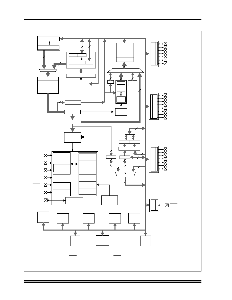
FIGURE 1-1:
PIC18F2450 (28-PIN) BLOCK DIAGRAM
Data Latch
Data Memory
(2 Kbytes)
Address Latch
Data Address<12>
12
Access
BSR
4
4
PCH PCL
PCLATH
8
31 Level Stack
Program Counter
PRODL
PRODH
8 x 8 Multiply
8
8
8
ALU<8>
Address Latch
Program Memory
(24/32 Kbytes)
Data Latch
20
8
8
Table Pointer<21>
inc/dec logic
21
8
Data Bus<8>
Table Latch
8
IR
12
3
ROM Latch
PCLATU
PCU
PORTE
MCLR/V
PP
/RE3
(1)
Note 1:
RE3 is multiplexed with MCLR and is only available when the MCLR Resets are disabled.
2:
OSC1/CLKI and OSC2/CLKO are only available in select oscillator modes and when these pins are not being used as digital I/O. Refer
to Section 2.0 "Oscillator Configurations" for additional information.
W
Instruction Bus <16>
STKPTR
Bank
8
8
8
BITOP
FSR0
FSR1
FSR2
inc/dec
Address
12
Decode
logic
EUSART
Timer2
Timer1
Timer0
USB
Instruction
Decode &
Control
State Machine
Control Signals
Power-up
Timer
Oscillator
Start-up Timer
Power-on
Reset
Watchdog
Timer
OSC1
(2)
OSC2
(2)
V
DD
,
Brown-out
Reset
Internal
Oscillator
Fail-Safe
Clock Monitor
Reference
Band Gap
V
SS
MCLR
(1)
Block
INTRC
Oscillator
Single-Supply
Programming
In-Circuit
Debugger
T1OSI
T1OSO
USB Voltage
Regulator
V
USB
PORTB
PORTC
RB0/AN12/INT0
RC0/T1OSO/T1CKI
RC1/T1OSI/UOE
RC2/CCP1
RC4/D-/VM
RC5/D+/VP
RC6/TX/CK
RC7/RX/DT
RB1/AN10/INT1
RB2/AN8/INT2/VMO
RB3/AN9/VPO
RB4/AN11/KBI0
RB5/KBI1/PGM
RB6/KBI2/PGC
RB7/KBI3/PGD
PORTA
RA4/T0CKI/RCV
RA5/AN4/HLVDIN
RA3/AN3/V
REF
+
RA2/AN2/V
REF
-
RA1/AN1
RA0/AN0
OSC2/CLKO/RA6
CCP1
ADC
10-bit
BOR
HLVD
PIC18F2450/4450
� 2006 Microchip Technology Inc.
Advance Information
DS39760A-page 11
FIGURE 1-2:
PIC18F4450 (40/44-PIN) BLOCK DIAGRAM
Instruction
Decode &
Control
Data Latch
Data Memory
(2 Kbytes)
Address Latch
Data Address<12>
12
Access
BSR
4
4
PCH PCL
PCLATH
8
31 Level Stack
Program Counter
PRODL
PRODH
8 x 8 Multiply
8
BITOP
8
8
ALU<8>
Address Latch
Program Memory
(24/32 Kbytes)
Data Latch
20
8
8
Table Pointer<21>
inc/dec logic
21
8
Data Bus<8>
Table Latch
8
IR
12
3
ROM Latch
PORTD
PCLATU
PCU
PORTE
MCLR/V
PP
/RE3
(1)
RE2/AN7
RE0/AN5
RE1/AN6
Note 1:
RE3 is multiplexed with MCLR and is only available when the MCLR Resets are disabled.
2:
OSC1/CLKI and OSC2/CLKO are only available in select oscillator modes and when these pins are not being used as digital I/O. Refer
to Section 2.0 "Oscillator Configurations" for additional information.
3:
These pins are only available on 44-pin TQFP under certain conditions. Refer to Section 18.9 "Special ICPORT Features (Designated
Packages Only)" for additional information.
EUSART
10-bit
ADC
Timer2
Timer1
Timer0
CCP1
W
Instruction Bus <16>
STKPTR
Bank
8
State Machine
Control Signals
8
8
Power-up
Timer
Oscillator
Start-up Timer
Power-on
Reset
Watchdog
Timer
OSC1
(2)
OSC2
(2)
V
DD
,
Brown-out
Reset
Internal
Oscillator
Fail-Safe
Clock Monitor
Reference
Band Gap
V
SS
MCLR
(1)
Block
INTRC
Oscillator
Single-Supply
Programming
In-Circuit
Debugger
T1OSI
T1OSO
PORTA
PORTB
PORTC
RA4/T0CKI/RCV
RA5/AN4/HLVDIN
RB0/AN12/INT0
RC0/T1OSO/T1CKI
RC1/T1OSI/UOE
RC2/CCP1
RC4/D-/VM
RC5/D+/VP
RC6/TX/CK
RC7/RX/DT
RA3/AN3/V
REF
+
RA2/AN2/V
REF
-
RA1/AN1
RA0/AN0
RB1/AN10/INT1
RB2/AN8/INT2/VMO
RB3/AN9/VPO
OSC2/CLKO/RA6
RB4/AN11/KBI0
RB5/KBI1/PGM
RB6/KBI2/PGC
RB7/KBI3/PGD
USB
FSR0
FSR1
FSR2
inc/dec
Address
12
Decode
logic
USB Voltage
Regulator
V
USB
ICRST
(3)
ICPGC
(3)
ICPGD
(3)
ICPORTS
(3)
RD0
RD1
RD2
RD3
RD4
RD5
RD6
RD7
BOR
HLVD

PIC18F2450/4450
DS39760A-page 12
Advance Information
� 2006 Microchip Technology Inc.
TABLE 1-2:
PIC18F2450 PINOUT I/O DESCRIPTIONS
Pin Name
Pin Number
Pin
Type
Buffer
Type
Description
PDIP,
SOIC
QFN
MCLR/Vpp/RE3
MCLR
V
PP
RE3
1
26
I
P
I
ST
ST
Master Clear (input) or programming voltage (input).
Master Clear (Reset) input. This pin is an active-low
Reset to the device.
Programming voltage input.
Digital input.
OSC1/CLKI
OSC1
CLKI
9
6
I
I
Analog
Analog
Oscillator crystal or external clock input.
Oscillator crystal input or external clock source input.
External clock source input. Always associated with pin
function OSC1. (See OSC2/CLKO pin.)
OSC2/CLKO/RA6
OSC2
CLKO
RA6
10
7
O
O
I/O
--
--
TTL
Oscillator crystal or clock output.
Oscillator crystal output. Connects to crystal or resonator
in Crystal Oscillator mode.
In select modes, OSC2 pin outputs CLKO which has
1/4 the frequency of OSC1 and denotes the instruction
cycle rate.
General purpose I/O pin.
Legend: TTL = TTL compatible input
CMOS = CMOS compatible input or output
ST
= Schmitt Trigger input with CMOS levels
I
= Input
O
= Output
P
= Power

PIC18F2450/4450
� 2006 Microchip Technology Inc.
Advance Information
DS39760A-page 13
PORTA is a bidirectional I/O port.
RA0/AN0
RA0
AN0
2
27
I/O
I
TTL
Analog
Digital I/O.
Analog input 0.
RA1/AN1
RA1
AN1
3
28
I/O
I
TTL
Analog
Digital I/O.
Analog input 1.
RA2/AN2/V
REF
-
RA2
AN2
V
REF
-
4
1
I/O
I
I
TTL
Analog
Analog
Digital I/O.
Analog input 2.
A/D reference voltage (low) input.
RA3/AN3/V
REF
+
RA3
AN3
V
REF
+
5
2
I/O
I
I
TTL
Analog
Analog
Digital I/O.
Analog input 3.
A/D reference voltage (high) input.
RA4/T0CKI/RCV
RA4
T0CKI
RCV
6
3
I/O
I
I
ST
ST
TTL
Digital I/O.
Timer0 external clock input.
External USB transceiver RCV input.
RA5/AN4/HLVDIN
RA5
AN4
HLVDIN
7
4
I/O
I
I
TTL
Analog
Analog
Digital I/O.
Analog input 4.
High/Low-Voltage Detect input.
RA6
--
--
--
--
See the OSC2/CLKO/RA6 pin.
TABLE 1-2:
PIC18F2450 PINOUT I/O DESCRIPTIONS (CONTINUED)
Pin Name
Pin Number
Pin
Type
Buffer
Type
Description
PDIP,
SOIC
QFN
Legend: TTL = TTL compatible input
CMOS = CMOS compatible input or output
ST
= Schmitt Trigger input with CMOS levels
I
= Input
O
= Output
P
= Power

PIC18F2450/4450
DS39760A-page 14
Advance Information
� 2006 Microchip Technology Inc.
PORTB is a bidirectional I/O port. PORTB can be software
programmed for internal weak pull-ups on all inputs.
RB0/AN12/INT0
RB0
AN12
INT0
21
18
I/O
I
I
TTL
Analog
ST
Digital I/O.
Analog input 12.
External interrupt 0.
RB1/AN10/INT1
RB1
AN10
INT1
22
19
I/O
I
I
TTL
Analog
ST
Digital I/O.
Analog input 10.
External interrupt 1.
RB2/AN8/INT2/VMO
RB2
AN8
INT2
VMO
23
20
I/O
I
I
O
TTL
Analog
ST
--
Digital I/O.
Analog input 8.
External interrupt 2.
External USB transceiver VMO output.
RB3/AN9/VPO
RB3
AN9
VPO
24
21
I/O
I
O
TTL
Analog
--
Digital I/O.
Analog input 9.
External USB transceiver VPO output.
RB4/AN11/KBI0
RB4
AN11
KBI0
25
22
I/O
I
I
TTL
Analog
TTL
Digital I/O.
Analog input 11.
Interrupt-on-change pin.
RB5/KBI1/PGM
RB5
KBI1
PGM
26
23
I/O
I
I/O
TTL
TTL
ST
Digital I/O.
Interrupt-on-change pin.
Low-Voltage ICSPTM Programming enable pin.
RB6/KBI2/PGC
RB6
KBI2
PGC
27
24
I/O
I
I/O
TTL
TTL
ST
Digital I/O.
Interrupt-on-change pin.
In-Circuit Debugger and ICSP programming clock pin.
RB7/KBI3/PGD
RB7
KBI3
PGD
28
25
I/O
I
I/O
TTL
TTL
ST
Digital I/O.
Interrupt-on-change pin.
In-Circuit Debugger and ICSP programming data pin.
TABLE 1-2:
PIC18F2450 PINOUT I/O DESCRIPTIONS (CONTINUED)
Pin Name
Pin Number
Pin
Type
Buffer
Type
Description
PDIP,
SOIC
QFN
Legend: TTL = TTL compatible input
CMOS = CMOS compatible input or output
ST
= Schmitt Trigger input with CMOS levels
I
= Input
O
= Output
P
= Power
PIC18F2450/4450
� 2006 Microchip Technology Inc.
Advance Information
DS39760A-page 15
PORTC is a bidirectional I/O port.
RC0/T1OSO/T1CKI
RC0
T1OSO
T1CKI
11
8
I/O
O
I
ST
--
ST
Digital I/O.
Timer1 oscillator output.
Timer1external clock input.
RC1/T1OSI/UOE
RC1
T1OSI
UOE
12
9
I/O
I
--
ST
CMOS
--
Digital I/O.
Timer1 oscillator input.
External USB transceiver OE output.
RC2/CCP1
RC2
CCP1
13
10
I/O
I/O
ST
ST
Digital I/O.
Capture 1 input/Compare 1 output/PWM 1 output.
RC4/D-/VM
RC4
D-
VM
15
12
I
I/O
I
TTL
--
TTL
Digital input.
USB differential minus line (input/output).
External USB transceiver VM input.
RC5/D+/VP
RC5
D+
VP
16
13
I
I/O
O
TTL
--
TTL
Digital input.
USB differential plus line (input/output).
External USB transceiver VP input.
RC6/TX/CK
RC6
TX
CK
17
14
I/O
O
I/O
ST
--
ST
Digital I/O.
EUSART asynchronous transmit.
EUSART synchronous clock (see RX/DT).
RC7/RX/DT
RC7
RX
DT
18
15
I/O
I
I/O
ST
ST
ST
Digital I/O.
EUSART asynchronous receive.
EUSART synchronous data (see TX/CK).
RE3
--
--
--
--
See MCLR/V
PP
/RE3 pin.
V
USB
14
11
O
--
Internal USB 3.3V voltage regulator.
V
SS
8, 19 5, 16
P
--
Ground reference for logic and I/O pins.
V
DD
20
17
P
--
Positive supply for logic and I/O pins.
TABLE 1-2:
PIC18F2450 PINOUT I/O DESCRIPTIONS (CONTINUED)
Pin Name
Pin Number
Pin
Type
Buffer
Type
Description
PDIP,
SOIC
QFN
Legend: TTL = TTL compatible input
CMOS = CMOS compatible input or output
ST
= Schmitt Trigger input with CMOS levels
I
= Input
O
= Output
P
= Power

PIC18F2450/4450
DS39760A-page 16
Advance Information
� 2006 Microchip Technology Inc.
TABLE 1-3:
PIC18F4450 PINOUT I/O DESCRIPTIONS
Pin Name
Pin Number
Pin
Type
Buffer
Type
Description
PDIP
QFN
TQFP
MCLR/Vpp/RE3
MCLR
V
PP
RE3
1
18
18
I
P
I
ST
ST
Master Clear (input) or programming voltage (input).
Master Clear (Reset) input. This pin is an
active-low Reset to the device.
Programming voltage input.
Digital input.
OSC1/CLKI
OSC1
CLKI
13
32
30
I
I
Analog
Analog
Oscillator crystal or external clock input.
Oscillator crystal input or external clock source input.
External clock source input. Always associated with
pin function OSC1. (See OSC2/CLKO pin.)
OSC2/CLKO/RA6
OSC2
CLKO
RA6
14
33
31
O
O
I/O
--
--
TTL
Oscillator crystal or clock output.
Oscillator crystal output. Connects to crystal or
resonator in Crystal Oscillator mode.
In select modes, OSC2 pin outputs CLKO which has
1/4 the frequency of OSC1 and denotes the instruction
cycle rate.
General purpose I/O pin.
Legend: TTL = TTL compatible input
CMOS = CMOS compatible input or output
ST
= Schmitt Trigger input with CMOS levels
I
= Input
O
= Output
P
= Power
Note 1:
These pins are No Connect unless the ICPRT Configuration bit is set. For NC/ICPORTS, the pin is No
Connect unless ICPRT is set and the DEBUG Configuration bit is cleared.

PIC18F2450/4450
� 2006 Microchip Technology Inc.
Advance Information
DS39760A-page 17
PORTA is a bidirectional I/O port.
RA0/AN0
RA0
AN0
2
19
19
I/O
I
TTL
Analog
Digital I/O.
Analog input 0.
RA1/AN1
RA1
AN1
3
20
20
I/O
I
TTL
Analog
Digital I/O.
Analog input 1.
RA2/AN2/V
REF
-
RA2
AN2
V
REF
-
4
21
21
I/O
I
I
TTL
Analog
Analog
Digital I/O.
Analog input 2.
A/D reference voltage (low) input.
RA3/AN3/V
REF
+
RA3
AN3
V
REF
+
5
22
22
I/O
I
I
TTL
Analog
Analog
Digital I/O.
Analog input 3.
A/D reference voltage (high) input.
RA4/T0CKI/RCV
RA4
T0CKI
RCV
6
23
23
I/O
I
I
ST
ST
TTL
Digital I/O.
Timer0 external clock input.
External USB transceiver RCV input.
RA5/AN4/HLVDIN
RA5
AN4
HLVDIN
7
24
24
I/O
I
I
TTL
Analog
Analog
Digital I/O.
Analog input 4.
High/Low-Voltage Detect input.
RA6
--
--
--
--
--
See the OSC2/CLKO/RA6 pin.
TABLE 1-3:
PIC18F4450 PINOUT I/O DESCRIPTIONS (CONTINUED)
Pin Name
Pin Number
Pin
Type
Buffer
Type
Description
PDIP
QFN
TQFP
Legend: TTL = TTL compatible input
CMOS = CMOS compatible input or output
ST
= Schmitt Trigger input with CMOS levels
I
= Input
O
= Output
P
= Power
Note 1:
These pins are No Connect unless the ICPRT Configuration bit is set. For NC/ICPORTS, the pin is No
Connect unless ICPRT is set and the DEBUG Configuration bit is cleared.

PIC18F2450/4450
DS39760A-page 18
Advance Information
� 2006 Microchip Technology Inc.
PORTB is a bidirectional I/O port. PORTB can be
software programmed for internal weak pull-ups on all
inputs.
RB0/AN12/INT0
RB0
AN12
INT0
33
9
8
I/O
I
I
TTL
Analog
ST
Digital I/O.
Analog input 12.
External interrupt 0.
RB1/AN10/INT1
RB1
AN10
INT1
34
10
9
I/O
I
I
TTL
Analog
ST
Digital I/O.
Analog input 10.
External interrupt 1.
RB2/AN8/INT2/VMO
RB2
AN8
INT2
VMO
35
11
10
I/O
I
I
O
TTL
Analog
ST
--
Digital I/O.
Analog input 8.
External interrupt 2.
External USB transceiver VMO output.
RB3/AN9/VPO
RB3
AN9
VPO
36
12
11
I/O
I
O
TTL
Analog
--
Digital I/O.
Analog input 9.
External USB transceiver VPO output.
RB4/AN11/KBI0
RB4
AN11
KBI0
37
14
14
I/O
I
I
TTL
Analog
TTL
Digital I/O.
Analog input 11.
Interrupt-on-change pin.
RB5/KBI1/PGM
RB5
KBI1
PGM
38
15
15
I/O
I
I/O
TTL
TTL
ST
Digital I/O.
Interrupt-on-change pin.
Low-Voltage ICSPTM Programming enable pin.
RB6/KBI2/PGC
RB6
KBI2
PGC
39
16
16
I/O
I
I/O
TTL
TTL
ST
Digital I/O.
Interrupt-on-change pin.
In-Circuit Debugger and ICSP programming clock pin.
RB7/KBI3/PGD
RB7
KBI3
PGD
40
17
17
I/O
I
I/O
TTL
TTL
ST
Digital I/O.
Interrupt-on-change pin.
In-Circuit Debugger and ICSP programming data pin.
TABLE 1-3:
PIC18F4450 PINOUT I/O DESCRIPTIONS (CONTINUED)
Pin Name
Pin Number
Pin
Type
Buffer
Type
Description
PDIP
QFN
TQFP
Legend: TTL = TTL compatible input
CMOS = CMOS compatible input or output
ST
= Schmitt Trigger input with CMOS levels
I
= Input
O
= Output
P
= Power
Note 1:
These pins are No Connect unless the ICPRT Configuration bit is set. For NC/ICPORTS, the pin is No
Connect unless ICPRT is set and the DEBUG Configuration bit is cleared.

PIC18F2450/4450
� 2006 Microchip Technology Inc.
Advance Information
DS39760A-page 19
PORTC is a bidirectional I/O port.
RC0/T1OSO/T1CKI
RC0
T1OSO
T1CKI
15
34
32
I/O
O
I
ST
--
ST
Digital I/O.
Timer1 oscillator output.
Timer1 external clock input.
RC1/T1OSI/UOE
RC1
T1OSI
UOE
16
35
35
I/O
I
O
ST
CMOS
--
Digital I/O.
Timer1 oscillator input.
External USB transceiver OE output.
RC2/CCP1
RC2
CCP1
17
36
36
I/O
I/O
ST
ST
Digital I/O.
Capture 1 input/Compare 1 output/PWM 1 output.
RC4/D-/VM
RC4
D-
VM
23
42
42
I
I/O
I
TTL
--
TTL
Digital input.
USB differential minus line (input/output).
External USB transceiver VM input.
RC5/D+/VP
RC5
D+
VP
24
43
43
I
I/O
I
TTL
--
TTL
Digital input.
USB differential plus line (input/output).
External USB transceiver VP input.
RC6/TX/CK
RC6
TX
CK
25
44
44
I/O
O
I/O
ST
--
ST
Digital I/O.
EUSART asynchronous transmit.
EUSART synchronous clock (see RX/DT).
RC7/RX/DT
RC7
RX
DT
26
1
1
I/O
I
I/O
ST
ST
ST
Digital I/O.
EUSART asynchronous receive.
EUSART synchronous data (see TX/CK).
TABLE 1-3:
PIC18F4450 PINOUT I/O DESCRIPTIONS (CONTINUED)
Pin Name
Pin Number
Pin
Type
Buffer
Type
Description
PDIP
QFN
TQFP
Legend: TTL = TTL compatible input
CMOS = CMOS compatible input or output
ST
= Schmitt Trigger input with CMOS levels
I
= Input
O
= Output
P
= Power
Note 1:
These pins are No Connect unless the ICPRT Configuration bit is set. For NC/ICPORTS, the pin is No
Connect unless ICPRT is set and the DEBUG Configuration bit is cleared.

PIC18F2450/4450
DS39760A-page 20
Advance Information
� 2006 Microchip Technology Inc.
PORTD is a bidirectional I/O port.
RD0
19
38
38
I/O
ST
Digital I/O.
RD1
20
39
39
I/O
ST
Digital I/O.
RD2
21
40
40
I/O
ST
Digital I/O.
RD3
22
41
41
I/O
ST
Digital I/O.
RD4
27
2
2
I/O
ST
Digital I/O.
RD5
28
3
3
I/O
ST
Digital I/O.
RD6
29
4
4
I/O
ST
Digital I/O.
RD7
30
5
5
I/O
ST
Digital I/O.
TABLE 1-3:
PIC18F4450 PINOUT I/O DESCRIPTIONS (CONTINUED)
Pin Name
Pin Number
Pin
Type
Buffer
Type
Description
PDIP
QFN
TQFP
Legend: TTL = TTL compatible input
CMOS = CMOS compatible input or output
ST
= Schmitt Trigger input with CMOS levels
I
= Input
O
= Output
P
= Power
Note 1:
These pins are No Connect unless the ICPRT Configuration bit is set. For NC/ICPORTS, the pin is No
Connect unless ICPRT is set and the DEBUG Configuration bit is cleared.
PIC18F2450/4450
� 2006 Microchip Technology Inc.
Advance Information
DS39760A-page 21
PORTE is a bidirectional I/O port.
RE0/AN5
RE0
AN5
8
25
25
I/O
I
ST
Analog
Digital I/O.
Analog input 5.
RE1/AN6
RE1
AN6
9
26
26
I/O
I
ST
Analog
Digital I/O.
Analog input 6.
RE2/AN7
RE2
AN7
10
27
27
I/O
I
ST
Analog
Digital I/O.
Analog input 7.
RE3
--
--
--
--
--
See MCLR/V
PP
/RE3 pin.
V
SS
12, 31 6, 30,
31
6, 29
P
--
Ground reference for logic and I/O pins.
V
DD
11, 32
7, 8,
28, 29
7, 28
P
--
Positive supply for logic and I/O pins.
V
USB
18
37
37
O
--
Internal USB 3.3V voltage regulator output.
NC/ICCK/ICPGC
(1)
ICCK
ICPGC
--
--
12
I/O
I/O
ST
ST
No Connect or dedicated ICD/ICSPTM port clock.
In-Circuit Debugger clock.
ICSP programming clock.
NC/ICDT/ICPGD
(1)
ICDT
ICPGD
--
--
13
I/O
I/O
ST
ST
No Connect or dedicated ICD/ICSP port clock.
In-Circuit Debugger data.
ICSP programming data.
NC/ICRST/ICV
PP
(1)
ICRST
ICV
PP
--
--
33
I
P
--
--
No Connect or dedicated ICD/ICSP port Reset.
Master Clear (Reset) input.
Programming voltage input.
NC/ICPORTS
(1)
ICPORTS
--
--
34
P
--
No Connect or 28-pin device emulation.
Enable 28-pin device emulation when connected
to V
SS
.
NC
--
13
--
--
--
No Connect.
TABLE 1-3:
PIC18F4450 PINOUT I/O DESCRIPTIONS (CONTINUED)
Pin Name
Pin Number
Pin
Type
Buffer
Type
Description
PDIP
QFN
TQFP
Legend: TTL = TTL compatible input
CMOS = CMOS compatible input or output
ST
= Schmitt Trigger input with CMOS levels
I
= Input
O
= Output
P
= Power
Note 1:
These pins are No Connect unless the ICPRT Configuration bit is set. For NC/ICPORTS, the pin is No
Connect unless ICPRT is set and the DEBUG Configuration bit is cleared.

PIC18F2450/4450
DS39760A-page 22
Advance Information
� 2006 Microchip Technology Inc.
NOTES:

PIC18F2450/4450
� 2006 Microchip Technology Inc.
Advance Information
DS39760A-page 23
2.0
OSCILLATOR
CONFIGURATIONS
2.1
Overview
Devices in the PIC18F2450/4450 family incorporate a
different oscillator and microcontroller clock system
than the non-USB PIC18F devices. The addition of the
USB module, with its unique requirements for a stable
clock source, make it necessary to provide a separate
clock source that is compliant with both USB low-speed
and full-speed specifications.
To accommodate these requirements, PIC18F2450/
4450 devices include a new clock branch to provide a
48 MHz clock for full-speed USB operation. Since it is
driven from the primary clock source, an additional
system of prescalers and postscalers has been added
to accommodate a wide range of oscillator frequencies.
An overview of the oscillator structure is shown in
Figure 2-1.
Other oscillator features used in PIC18 enhanced
microcontrollers, such as the internal RC oscillator and
clock switching, remain the same. They are discussed
later in this chapter.
2.1.1
OSCILLATOR CONTROL
The operation of the oscillator in PIC18F2450/4450
devices is controlled through two Configuration
registers and two control registers. Configuration
registers, CONFIG1L and CONFIG1H, select the
oscillator mode and USB prescaler/postscaler options.
As Configuration bits, these are set when the device is
programmed and left in that configuration until the
device is reprogrammed.
The OSCCON register (Register 2-1) selects the Active
Clock mode; it is primarily used in controlling clock
switching in power-managed modes. Its use is
discussed in Section 2.4.1 "Oscillator Control
Register".
2.2
Oscillator Types
PIC18F2450/4450 devices can be operated in twelve
distinct oscillator modes. In contrast with the non-USB
PIC18 enhanced microcontrollers, four of these modes
involve the use of two oscillator types at once. Users
can program the FOSC3:FOSC0 Configuration bits to
select one of these modes:
1.
XT
Crystal/Resonator
2.
XTPLL
Crystal/Resonator with PLL enabled
3.
HS
High-Speed Crystal/Resonator
4.
HSPLL
High-Speed Crystal/Resonator
with PLL enabled
5.
EC
External Clock with F
OSC
/4 output
6.
ECIO
External Clock with I/O on RA6
7.
ECPLL
External Clock with PLL enabled
and F
OSC
/4 output on RA6
8.
ECPIO
External Clock with PLL enabled,
I/O on RA6
9.
INTHS
Internal Oscillator used as
microcontroller clock source, HS
Oscillator used as USB clock source
10. INTXT
Internal Oscillator used as
microcontroller clock source, XT
Oscillator used as USB clock source
11. INTIO
Internal Oscillator used as
microcontroller clock source, EC
Oscillator used as USB clock source,
digital I/O on RA6
12. INTCKO Internal Oscillator used as
microcontroller clock source, EC
Oscillator used as USB clock source,
F
OSC
/4 output on RA6
PIC18F2450/4450
DS39760A-page 24
Advance Information
� 2006 Microchip Technology Inc.
2.2.1
OSCILLATOR MODES AND
USB OPERATION
Because of the unique requirements of the USB module,
a different approach to clock operation is necessary. In
previous PICmicro
�
devices, all core and peripheral
clocks were driven by a single oscillator source; the usual
sources were primary, secondary or the internal
oscillator. With PIC18F2450/4450 devices, the primary
oscillator becomes part of the USB module and cannot
be associated to any other clock source. Thus, the USB
module must be clocked from the primary clock source;
however, the microcontroller core and other peripherals
can be separately clocked from the secondary or internal
oscillators as before.
Because of the timing requirements imposed by USB,
an internal clock of either 6 MHz or 48 MHz is required
while the USB module is enabled. Fortunately, the
microcontroller and other peripherals are not required
to run at this clock speed when using the primary
oscillator. There are numerous options to achieve the
USB module clock requirement and still provide
flexibility for clocking the rest of the device from the
primary oscillator source. These are detailed in
Section 2.3 "Oscillator Settings for USB".
FIGURE 2-1:
PIC18F2450/4450 CLOCK DIAGRAM
PIC18F2450/4450
FOSC3:FOSC0
Secondary Oscillator
T1OSCEN
Enable
Oscillator
T1OSO
T1OSI
Clock Source Option
for other Modules
OSC1
OSC2
Sleep
Primary Oscillator
XT, HS, EC, ECIO
T1OSC
CPU
Peripherals
IDLEN
MU
X
OSCCON<6:4>
WDT, PWRT, FSCM
Internal Oscillator
Clock
Control
OSCCON<1:0>
and Two-Speed Start-up
96 MHz
PLL
PLLDIV
CPUDIV
0
1
0
1
� 2
P
L
L P
r
esca
ler
MU
X
111
110
101
100
011
010
001
000
� 1
� 2
� 3
� 4
� 5
� 6
� 10
� 12
11
10
01
00
P
L
L P
o
st
sca
ler
� 2
� 3
� 4
� 6
USB
USBDIV
FOSC3:FOSC0
HSPLL, ECPLL,
11
10
01
00
Oscill
a
t
or
P
o
st
scaler
� 1
� 2
� 3
� 4
CPUDIV
1
0
Peripheral
FSEN
� 4
USB Clock Source
XTPLL, ECPIO
Primary
Clock
(4 MHz Input Only)
Internal RC Oscillator
31.25 kHz
PIC18F2450/4450
� 2006 Microchip Technology Inc.
Advance Information
DS39760A-page 25
2.2.2
CRYSTAL OSCILLATOR/CERAMIC
RESONATORS
In HS, HSPLL, XT and XTPLL Oscillator modes, a
crystal or ceramic resonator is connected to the OSC1
and OSC2 pins to establish oscillation. Figure 2-2
shows the pin connections.
The oscillator design requires the use of a parallel cut
crystal.
FIGURE 2-2:
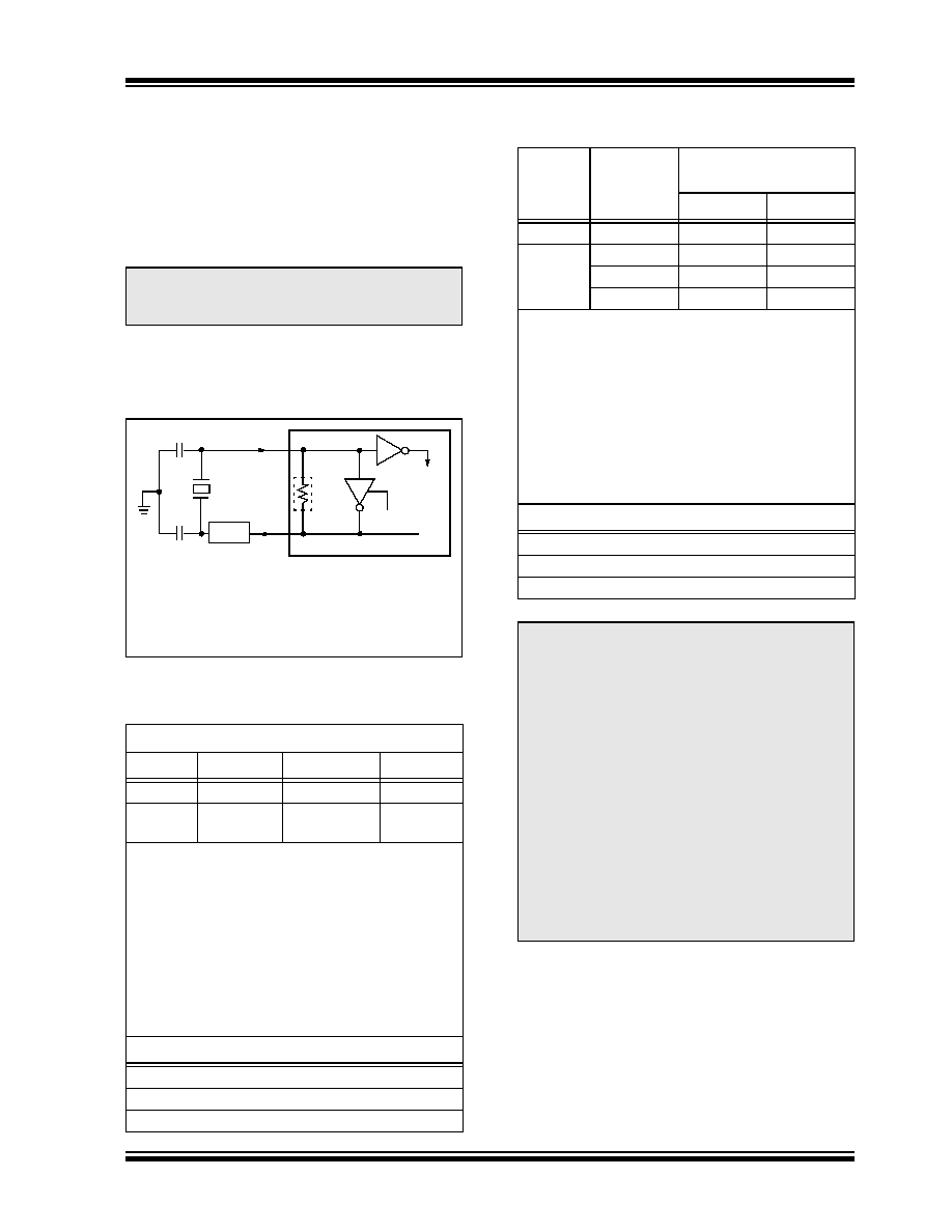
CRYSTAL/CERAMIC
RESONATOR OPERATION
(XT, HS OR HSPLL
CONFIGURATION)
TABLE 2-1:
CAPACITOR SELECTION FOR
CERAMIC RESONATORS
TABLE 2-2:
CAPACITOR SELECTION FOR
CRYSTAL OSCILLATOR
An internal postscaler allows users to select a clock
frequency other than that of the crystal or resonator.
Frequency division is determined by the CPUDIV Con-
figuration bits. Users may select a clock frequency of
the oscillator frequency, or 1/2, 1/3 or 1/4 of the
frequency.
An external clock may also be used when the micro-
controller is in HS Oscillator mode. In this case, the
OSC2/CLKO pin is left open (Figure 2-3).
Note:
Use of a series cut crystal may give a fre-
quency out of the crystal manufacturer's
specifications.
Typical Capacitor Values Used:
Mode
Freq
OSC1
OSC2
XT
4.0 MHz
33 pF
33 pF
HS
8.0 MHz
16.0 MHz
27 pF
22 pF
27 pF
22 pF
Capacitor values are for design guidance only.
These capacitors were tested with the resonators
listed below for basic start-up and operation. These
values are not optimized.
Different capacitor values may be required to produce
acceptable oscillator operation. The user should test
the performance of the oscillator over the expected
V
DD
and temperature range for the application.
See the notes following Table 2-2 for additional
information.
Resonators Used:
4.0 MHz
8.0 MHz
16.0 MHz
Note 1:
See Table 2-1 and Table 2-2 for initial values of
C1 and C2.
2: A series resistor (R
S
) may be required for AT
strip cut crystals.
3: R
F
varies with the oscillator mode chosen.
C1
(1)
C2
(1)
XTAL
OSC2
OSC1
R
F
(3)
Sleep
To
Logic
PIC18FXXXX
R
S
(2)
Internal
Osc Type
Crystal
Freq
Typical Capacitor Values
Tested:
C1
C2
XT
4 MHz
27 pF
27 pF
HS
4 MHz
27 pF
27 pF
8 MHz
22 pF
22 pF
20 MHz
15 pF
15 pF
Capacitor values are for design guidance only.
These capacitors were tested with the crystals listed
below for basic start-up and operation. These values
are not optimized.
Different capacitor values may be required to produce
acceptable oscillator operation. The user should test
the performance of the oscillator over the expected
V
DD
and temperature range for the application.
See the notes following this table for additional
information.
Crystals Used:
4 MHz
8 MHz
20 MHz
Note 1: Higher capacitance increases the stability
of oscillator but also increases the start-
up time.
2: When operating below 3V V
DD
, or when
using certain ceramic resonators at any
voltage, it may be necessary to use the
HS mode or switch to a crystal oscillator.
3: Since each resonator/crystal has its own
characteristics, the user should consult
the resonator/crystal manufacturer for
appropriate values of external
components.
4: Rs may be required to avoid overdriving
crystals with low drive level specification.
5: Always verify oscillator performance over
the V
DD
and temperature range that is
expected for the application.
PIC18F2450/4450
DS39760A-page 26
Advance Information
� 2006 Microchip Technology Inc.
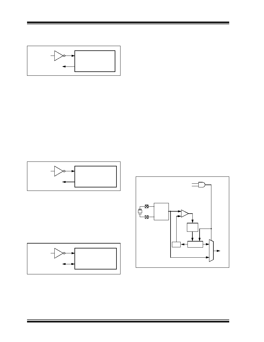
FIGURE 2-3:
EXTERNAL CLOCK INPUT
OPERATION (HS OSC
CONFIGURATION)
2.2.3
EXTERNAL CLOCK INPUT
The EC, ECIO, ECPLL and ECPIO Oscillator modes
require an external clock source to be connected to the
OSC1 pin. There is no oscillator start-up time required
after a Power-on Reset or after an exit from Sleep
mode.
In the EC and ECPLL Oscillator modes, the oscillator
frequency divided by 4 is available on the OSC2 pin.
This signal may be used for test purposes or to
synchronize other logic. Figure 2-4 shows the pin
connections for the EC Oscillator mode.
FIGURE 2-4:
EXTERNAL CLOCK
INPUT OPERATION
(EC AND ECPLL
CONFIGURATION)
The ECIO and ECPIO Oscillator modes function like the
EC and ECPLL modes, except that the OSC2 pin
becomes an additional general purpose I/O pin. The I/O
pin becomes bit 6 of PORTA (RA6). Figure 2-5 shows
the pin connections for the ECIO Oscillator mode.
FIGURE 2-5:
EXTERNAL CLOCK
INPUT OPERATION
(ECIO AND ECPIO
CONFIGURATION)
The internal postscaler for reducing clock frequency in
XT and HS modes is also available in EC and ECIO
modes.
2.2.4
PLL FREQUENCY MULTIPLIER
PIC18F2450/4450 devices include a Phase Locked
Loop (PLL) circuit. This is provided specifically for USB
applications with lower speed oscillators and can also
be used as a microcontroller clock source.
The PLL is enabled in HSPLL, XTPLL, ECPLL and
ECPIO Oscillator modes. It is designed to produce a
fixed 96 MHz reference clock from a fixed 4 MHz input.
The output can then be divided and used for both the
USB and the microcontroller core clock. Because the
PLL has a fixed frequency input and output, there are
eight prescaling options to match the oscillator input
frequency to the PLL.
There is also a separate postscaler option for deriving
the microcontroller clock from the PLL. This allows the
USB peripheral and microcontroller to use the same
oscillator input and still operate at different clock
speeds. In contrast to the postscaler for XT, HS and EC
modes, the available options are 1/2, 1/3, 1/4 and 1/6
of the PLL output.
The HSPLL, ECPLL and ECPIO modes make use of
the HS mode oscillator for frequencies up to 48 MHz.
The prescaler divides the oscillator input by up to 12 to
produce the 4 MHz drive for the PLL. The XTPLL mode
can only use an input frequency of 4 MHz which drives
the PLL directly.
FIGURE 2-6:
PLL BLOCK DIAGRAM
(HS MODE)
OSC1
OSC2
Open
Clock from
Ext. System
PIC18FXXXX
(HS Mode)
OSC1/CLKI
OSC2/CLKO
F
OSC
/4
Clock from
Ext. System
PIC18FXXXX
OSC1/CLKI
I/O (OSC2)
RA6
Clock from
Ext. System
PIC18FXXXX
MU
X
VCO
Loop
Filter
and
Prescaler
OSC2
OSC1
PLL Enable
F
IN
F
OUT
SYSCLK
Phase
Comparator
HS/EC/ECIO/XT Oscillator Enable
�24
(from CONFIG1H Register)
Oscillator

PIC18F2450/4450
� 2006 Microchip Technology Inc.
Advance Information
DS39760A-page 27
2.2.5
INTERNAL OSCILLATOR
The PIC18F2450/4450 devices include an internal RC
oscillator (INTRC) which provides a nominal 31 kHz out-
put. INTRC is enabled if it is selected as the device clock
source; it is also enabled automatically when any of the
following are enabled:
� Power-up Timer
� Fail-Safe Clock Monitor
� Watchdog Timer
� Two-Speed Start-up
These features are discussed in greater detail in
Section 18.0 "Special Features of the CPU".
2.2.5.1
Internal Oscillator Modes
When the internal oscillator is used as the micro-
controller clock source, one of the other oscillator
modes (External Clock or External Crystal/Resonator)
must be used as the USB clock source. The choice of
USB clock source is determined by the particular
internal oscillator mode.
There are four distinct modes available:
1.
INTHS mode: The USB clock is provided by the
oscillator in HS mode.
2.
INTXT mode: The USB clock is provided by the
oscillator in XT mode.
3.
INTCKO mode: The USB clock is provided by an
external clock input on OSC1/CLKI; the OSC2/
CLKO pin outputs F
OSC
/4.
4.
INTIO mode: The USB clock is provided by an
external clock input on OSC1/CLKI; the OSC2/
CLKO pin functions as a digital I/O (RA6).
Of these four modes, only INTIO mode frees up an
additional pin (OSC2/CLKO/RA6) for port I/O use.
2.3
Oscillator Settings for USB
When the PIC18F2450/4450 is used for USB
connectivity, it must have either a 6 MHz or 48 MHz
clock for USB operation, depending on whether Low-
Speed or Full-Speed mode is being used. This may
require some forethought in selecting an oscillator
frequency and programming the device.
The full range of possible oscillator configurations
compatible with USB operation is shown in Table 2-3.
2.3.1
LOW-SPEED OPERATION
The USB clock for Low-Speed mode is derived from
the primary oscillator chain and not directly from the
PLL. It is divided by 4 to produce the actual 6 MHz
clock. Because of this, the microcontroller can only use
a clock frequency of 24 MHz when the USB module is
active and the controller clock source is one of the
primary oscillator modes (XT, HS or EC, with or without
the PLL).
This restriction does not apply if the microcontroller
clock source is the secondary oscillator or internal
oscillator.
2.3.2
RUNNING DIFFERENT USB AND
MICROCONTROLLER CLOCKS
The USB module, in either mode, can run
asynchronously with respect to the microcontroller core
and other peripherals. This means that applications can
use the primary oscillator for the USB clock while the
microcontroller runs from a separate clock source at a
lower speed. If it is necessary to run the entire
application from only one clock source, full-speed
operation provides a greater selection of microcontroller
clock frequencies.

PIC18F2450/4450
DS39760A-page 28
Advance Information
� 2006 Microchip Technology Inc.
TABLE 2-3:
OSCILLATOR CONFIGURATION OPTIONS FOR USB OPERATION
Input Oscillator
Frequency
PLL Division
(PLLDIV2:PLLDIV0)
Clock Mode
(FOSC3:FOSC0)
MCU Clock Division
(CPUDIV1:CPUDIV0)
Microcontroller
Clock Frequency
48 MHz
N/A
(1)
EC, ECIO
None (00)
48 MHz
�2 (01)
24 MHz
�3 (10)
16 MHz
�4 (11)
12 MHz
48 MHz
�12 (111)
EC, ECIO
None (00)
48 MHz
�2 (01)
24 MHz
�3 (10)
16 MHz
�4 (11)
12 MHz
ECPLL, ECPIO
�2 (00)
48 MHz
�3 (01)
32 MHz
�4 (10)
24 MHz
�6 (11)
16 MHz
40 MHz
�10 (110)
EC, ECIO
None (00)
40 MHz
�2 (01)
20 MHz
�3 (10)
13.33 MHz
�4 (11)
10 MHz
ECPLL, ECPIO
�2 (00)
48 MHz
�3 (01)
32 MHz
�4 (10)
24 MHz
�6 (11)
16 MHz
24 MHz
�6 (101)
HS, EC, ECIO
None (00)
24 MHz
�2 (01)
12 MHz
�3 (10)
8 MHz
�4 (11)
6 MHz
HSPLL, ECPLL, ECPIO
�2 (00)
48 MHz
�3 (01)
32 MHz
�4 (10)
24 MHz
�6 (11)
16 MHz
20 MHz
�5 (100)
HS, EC, ECIO
None (00)
20 MHz
�2 (01)
10 MHz
�3 (10)
6.67 MHz
�4 (11)
5 MHz
HSPLL, ECPLL, ECPIO
�2 (00)
48 MHz
�3 (01)
32 MHz
�4 (10)
24 MHz
�6 (11)
16 MHz
16 MHz
�4 (011)
HS, EC, ECIO
None (00)
16 MHz
�2 (01)
8 MHz
�3 (10)
5.33 MHz
�4 (11)
4 MHz
HSPLL, ECPLL, ECPIO
�2 (00)
48 MHz
�3 (01)
32 MHz
�4 (10)
24 MHz
�6 (11)
16 MHz
Legend:
All clock frequencies, except 24 MHz, are exclusively associated with full-speed USB operation (USB clock of 48 MHz).
Bold is used to highlight clock selections that are compatible with low-speed USB operation (system clock of 24 MHz,
USB clock of 6 MHz).
Note
1:
Only valid when the USBDIV Configuration bit is cleared.

PIC18F2450/4450
� 2006 Microchip Technology Inc.
Advance Information
DS39760A-page 29
12 MHz
�3 (010)
HS, EC, ECIO
None (00)
12 MHz
�2 (01)
6 MHz
�3 (10)
4 MHz
�4 (11)
3 MHz
HSPLL, ECPLL, ECPIO
�2 (00)
48 MHz
�3 (01)
32 MHz
�4 (10)
24 MHz
�6 (11)
16 MHz
8 MHz
�2 (001)
HS, EC, ECIO
None (00)
8 MHz
�2 (01)
4 MHz
�3 (10)
2.67 MHz
�4 (11)
2 MHz
HSPLL, ECPLL, ECPIO
�2 (00)
48 MHz
�3 (01)
32 MHz
�4 (10)
24 MHz
�6 (11)
16 MHz
4 MHz
�1 (000)
XT, HS, EC, ECIO
None (00)
4 MHz
�2 (01)
2 MHz
�3 (10)
1.33 MHz
�4 (11)
1 MHz
HSPLL, ECPLL, XTPLL,
ECPIO
�2 (00)
48 MHz
�3 (01)
32 MHz
�4 (10)
24 MHz
�6 (11)
16 MHz
TABLE 2-3:
OSCILLATOR CONFIGURATION OPTIONS FOR USB OPERATION (CONTINUED)
Input Oscillator
Frequency
PLL Division
(PLLDIV2:PLLDIV0)
Clock Mode
(FOSC3:FOSC0)
MCU Clock Division
(CPUDIV1:CPUDIV0)
Microcontroller
Clock Frequency
Legend:
All clock frequencies, except 24 MHz, are exclusively associated with full-speed USB operation (USB clock of 48 MHz).
Bold is used to highlight clock selections that are compatible with low-speed USB operation (system clock of 24 MHz,
USB clock of 6 MHz).
Note
1:
Only valid when the USBDIV Configuration bit is cleared.

PIC18F2450/4450
DS39760A-page 30
Advance Information
� 2006 Microchip Technology Inc.
2.4
Clock Sources and Oscillator
Switching
Like previous PIC18 enhanced devices, the
PIC18F2450/4450 family includes a feature that allows
the device clock source to be switched from the main
oscillator to an alternate low-frequency clock source.
PIC18F2450/4450 devices offer two alternate clock
sources. When an alternate clock source is enabled,
the various power-managed operating modes are
available.
Essentially, there are three clock sources for these
devices:
� Primary oscillators
� Secondary oscillators
� Internal oscillator
The primary oscillators include the External Crystal
and Resonator modes, the External Clock modes and
the internal oscillator. The particular mode is defined by
the FOSC3:FOSC0 Configuration bits. The details of
these modes are covered earlier in this chapter.
The secondary oscillators are those external sources
not connected to the OSC1 or OSC2 pins. These
sources may continue to operate even after the
controller is placed in a power-managed mode.
PIC18F2450/4450 devices offer the Timer1 oscillator
as a secondary oscillator. This oscillator, in all power-
managed modes, is often the time base for functions
such as a Real-Time Clock. Most often, a 32.768 kHz
watch crystal is connected between the RC0/T1OSO/
T1CKI and RC1/T1OSI/UOE pins. Like the XT and HS
Oscillator mode circuits, loading capacitors are also
connected from each pin to ground. The Timer1
oscillator is discussed in greater detail in Section 11.3
"Timer1 Oscillator".
In addition to being a primary clock source, the internal
oscillator is available as a power-managed mode
clock source. The INTRC source is also used as the
clock source for several special features, such as the
WDT and Fail-Safe Clock Monitor.
2.4.1
OSCILLATOR CONTROL REGISTER
The OSCCON register (Register 2-1) controls several
aspects of the device clock's operation, both in full
power operation and in power-managed modes.
The System Clock Select bits, SCS1:SCS0, select the
clock source. The available clock sources are the
primary clock (defined by the FOSC3:FOSC0 Configura-
tion bits), the secondary clock (Timer1 oscillator) and the
internal oscillator. The clock source changes immedi-
ately after one or more of the bits is written to, following
a brief clock transition interval. The SCS bits are cleared
on all forms of Reset.
INTRC always remains the clock source for features
such as the Watchdog Timer and the Fail-Safe Clock
Monitor.
The OSTS and T1RUN bits indicate which clock source
is currently providing the device clock. The OSTS bit
indicates that the Oscillator Start-up Timer has timed out
and the primary clock is providing the device clock in
primary clock modes. The T1RUN bit (T1CON<6>) indi-
cates when the Timer1 oscillator is providing the device
clock in secondary clock modes. In power-managed
modes, only one of these three bits will be set at any
time. If none of these bits are set, the INTRC is providing
the clock or the internal oscillator has just started and is
not yet stable.
The IDLEN bit determines if the device goes into Sleep
mode, or one of the Idle modes, when the SLEEP
instruction is executed.
The use of the flag and control bits in the OSCCON
register is discussed in more detail in Section 3.0
"Power-Managed Modes".
2.4.2
OSCILLATOR TRANSITIONS
PIC18F2450/4450 devices contain circuitry to prevent
clock "glitches" when switching between clock sources.
A short pause in the device clock occurs during the
clock switch. The length of this pause is the sum of two
cycles of the old clock source and three to four cycles
of the new clock source. This formula assumes that the
new clock source is stable.
Clock transitions are discussed in greater detail in
Section 3.1.2 "Entering Power-Managed Modes".
Note 1: The Timer1 oscillator must be enabled to
select the secondary clock source. The
Timer1 oscillator is enabled by setting the
T1OSCEN bit in the Timer1 Control regis-
ter (T1CON<3>). If the Timer1 oscillator is
not enabled, then any attempt to select a
secondary clock source will be ignored.
2: It is recommended that the Timer1
oscillator be operating and stable prior to
switching to it as the clock source; other-
wise, a very long delay may occur while
the Timer1 oscillator starts.

PIC18F2450/4450
� 2006 Microchip Technology Inc.
Advance Information
DS39760A-page 31
REGISTER 2-1:
OSCCON: OSCILLATOR CONTROL REGISTER
R/W-0
U-0
U-0
U-0
R
(1)
U-0
R/W-0
R/W-0
IDLEN
--
--
--
OSTS
--
SCS1
SCS0
bit 7
bit 0
Legend:
R = Readable bit
W = Writable bit
U = Unimplemented bit, read as `0'
-n = Value at POR
`1' = Bit is set
`0' = Bit is cleared
x = Bit is unknown
bit 7
IDLEN: Idle Enable bit
1
= Device enters Idle mode on SLEEP instruction
0
= Device enters Sleep mode on SLEEP instruction
bit 6-4
Unimplemented: Read as `0'
bit 3
OSTS: Oscillator Start-up Time-out Status bit
(1)
1
= Oscillator Start-up Timer time-out has expired; primary oscillator is running
0
= Oscillator Start-up Timer time-out is running; primary oscillator is not ready
bit 2
Unimplemented: Read as `0'
bit 1-0
SCS1:SCS0: System Clock Select bits
1x
= Internal oscillator
01
= Timer1 oscillator
00
= Primary oscillator
Note 1:
Depends on the state of the IESO Configuration bit.

PIC18F2450/4450
DS39760A-page 32
Advance Information
� 2006 Microchip Technology Inc.
2.5
Effects of Power-Managed Modes
on the Various Clock Sources
When PRI_IDLE mode is selected, the designated
primary oscillator continues to run without interruption.
For all other power-managed modes, the oscillator
using the OSC1 pin is disabled. Unless the USB
module is enabled, the OSC1 pin (and OSC2 pin if
used by the oscillator) will stop oscillating.
In secondary clock modes (SEC_RUN and
SEC_IDLE), the Timer1 oscillator is operating and
providing the device clock. The Timer1 oscillator may
also run in all power-managed modes if required to
clock Timer1.
In internal oscillator modes (RC_RUN and RC_IDLE),
the internal oscillator provides the device clock source.
The 31 kHz INTRC output can be used directly to
provide the clock and may be enabled to support various
special features regardless of the power-managed
mode (see Section 18.2 "Watchdog Timer (WDT)",
Section 18.3 "Two-Speed Start-up" and Section 18.4
"Fail-Safe Clock Monitor" for more information on
WDT, Fail-Safe Clock Monitor and Two-Speed Start-up).
Regardless of the Run or Idle mode selected, the USB
clock source will continue to operate. If the device is
operating from a crystal or resonator-based oscillator,
that oscillator will continue to clock the USB module.
The core and all other modules will switch to the new
clock source.
If the Sleep mode is selected, all clock sources are
stopped. Since all the transistor switching currents
have been stopped, Sleep mode achieves the lowest
current consumption of the device (only leakage
currents).
Sleep mode should never be invoked while the USB
module is operating and connected. The only exception
is when the device has been issued a "Suspend" com-
mand over the USB. Once the module has suspended
operation and shifted to a low-power state, the
microcontroller may be safely put into Sleep mode.
Enabling any on-chip feature that will operate during
Sleep will increase the current consumed during Sleep.
The INTRC is required to support WDT operation. The
Timer1 oscillator may be operating to support a Real-
Time Clock. Other features may be operating that do
not require a device clock source (i.e., PSP, INTn pins
and others). Peripherals that may add significant
current consumption are listed in Section 21.2 "DC
Characteristics: Power-Down and Supply Current".
2.6
Power-up Delays
Power-up delays are controlled by two timers, so that no
external Reset circuitry is required for most applications.
The delays ensure that the device is kept in Reset until
the device power supply is stable under normal circum-
stances and the primary clock is operating and stable.
For additional information on power-up delays, see
Section 4.5 "Device Reset Timers".
The first timer is the Power-up Timer (PWRT), which
provides a fixed delay on power-up (parameter 33,
Table 21-10). It is enabled by clearing (= 0) the
PWRTEN Configuration bit.
The second timer is the Oscillator Start-up Timer
(OST), intended to keep the chip in Reset until the
crystal oscillator is stable (XT and HS modes). The
OST does this by counting 1024 oscillator cycles
before allowing the oscillator to clock the device.
When the HSPLL Oscillator mode is selected, the
device is kept in Reset for an additional 2 ms following
the HS mode OST delay, so the PLL can lock to the
incoming clock frequency.
There is a delay of interval, T
CSD
(parameter 38,
Table 21-10), following POR, while the controller
becomes ready to execute instructions. This delay runs
concurrently with any other delays. This may be the
only delay that occurs when any of the EC or internal
oscillator modes are used as the primary clock source.
TABLE 2-4:
OSC1 AND OSC2 PIN STATES IN SLEEP MODE
Oscillator Mode
OSC1 Pin
OSC2 Pin
INTCKO
Floating, pulled by external clock
At logic low (clock/4 output)
INTIO
Floating, pulled by external clock
Configured as PORTA, bit 6
ECIO, ECPIO
Floating, pulled by external clock
Configured as PORTA, bit 6
EC
Floating, pulled by external clock
At logic low (clock/4 output)
XT and HS
Feedback inverter disabled at quiescent
voltage level
Feedback inverter disabled at quiescent
voltage level
Note:
See Table 4-2 in Section 4.0 "Reset" for time-outs due to Sleep and MCLR Reset.

PIC18F2450/4450
� 2006 Microchip Technology Inc.
Advance Information
DS39760A-page 33
3.0
POWER-MANAGED MODES
PIC18F2450/4450 devices offer a total of seven
operating modes for more efficient power
management. These modes provide a variety of
options for selective power conservation in applications
where resources may be limited (i.e., battery-powered
devices).
There are three categories of power-managed modes:
� Run modes
� Idle modes
� Sleep mode
These categories define which portions of the device
are clocked and sometimes, what speed. The Run and
Idle modes may use any of the three available clock
sources (primary, secondary or internal oscillator); the
Sleep mode does not use a clock source.
The power-managed modes include several power-
saving features offered on previous PICmicro
�
devices. One is the clock switching feature, offered in
other PIC18 devices, allowing the controller to use the
Timer1 oscillator in place of the primary oscillator. Also
included is the Sleep mode, offered by all PICmicro
devices, where all device clocks are stopped.
3.1
Selecting Power-Managed Modes
Selecting a power-managed mode requires two
decisions: if the CPU is to be clocked or not and the
selection of a clock source. The IDLEN bit
(OSCCON<7>) controls CPU clocking, while the
SCS1:SCS0 bits (OSCCON<1:0>) select the clock
source. The individual modes, bit settings, clock sources
and affected modules are summarized in Table 3-1.
3.1.1
CLOCK SOURCES
The SCS1:SCS0 bits allow the selection of one of three
clock sources for power-managed modes. They are:
� The primary clock, as defined by the
FOSC3:FOSC0 Configuration bits
� The secondary clock (the Timer1 oscillator)
� The internal oscillator (for RC modes)
3.1.2
ENTERING POWER-MANAGED
MODES
Switching from one power-managed mode to another
begins by loading the OSCCON register. The
SCS1:SCS0 bits select the clock source and determine
which Run or Idle mode is to be used. Changing these
bits causes an immediate switch to the new clock
source, assuming that it is running. The switch may
also be subject to clock transition delays. These are
discussed in Section 3.1.3 "Clock Transitions and
Status Indicators" and subsequent sections.
Entry to the power-managed Idle or Sleep modes is
triggered by the execution of a SLEEP instruction. The
actual mode that results depends on the status of the
IDLEN bit.
Depending on the current mode and the mode being
switched to, a change to a power-managed mode does
not always require setting all of these bits. Many
transitions may be done by changing the oscillator
select bits, or changing the IDLEN bit, prior to issuing a
SLEEP
instruction. If the IDLEN bit is already
configured correctly, it may only be necessary to
perform a SLEEP instruction to switch to the desired
mode.
TABLE 3-1:
POWER-MANAGED MODES
Mode
OSCCON Bits
Module Clocking
Available Clock and Oscillator Source
IDLEN
(1)
SCS1:SCS0
CPU
Peripherals
Sleep
0
N/A
Off
Off
None � all clocks are disabled
PRI_RUN
N/A
00
Clocked
Clocked
Primary � all oscillator modes.
This is the normal full power execution mode.
SEC_RUN
N/A
01
Clocked
Clocked
Secondary � Timer1 oscillator
RC_RUN
N/A
1x
Clocked
Clocked
Internal oscillator
(2)
PRI_IDLE
1
00
Off
Clocked
Primary � all oscillator modes
SEC_IDLE
1
01
Off
Clocked
Secondary � Timer1 oscillator
RC_IDLE
1
1x
Off
Clocked
Internal oscillator
(2)
Note 1:
IDLEN reflects its value when the SLEEP instruction is executed.
2:
Clock is INTRC source.
PIC18F2450/4450
DS39760A-page 34
Advance Information
� 2006 Microchip Technology Inc.
3.1.3
CLOCK TRANSITIONS AND
STATUS INDICATORS
The length of the transition between clock sources is
the sum of two cycles of the old clock source and three
to four cycles of the new clock source. This formula
assumes that the new clock source is stable.
Two bits indicate the current clock source and its
status. They are:
� OSTS (OSCCON<3>)
� T1RUN (T1CON<6>)
In general, only one of these bits will be set while in a
given power-managed mode. When the OSTS bit is
set, the primary clock is providing the device clock.
When the T1RUN bit is set, the Timer1 oscillator is
providing the clock.
3.1.4
MULTIPLE SLEEP COMMANDS
The power-managed mode that is invoked with the
SLEEP
instruction is determined by the setting of the
IDLEN bit at the time the instruction is executed. If
another SLEEP instruction is executed, the device will
enter the power-managed mode specified by IDLEN at
that time. If IDLEN has changed, the device will enter
the new power-managed mode specified by the new
setting.
3.2
Run Modes
In the Run modes, clocks to both the core and
peripherals are active. The difference between these
modes is the clock source.
3.2.1
PRI_RUN MODE
The PRI_RUN mode is the normal, full power execution
mode of the microcontroller. This is also the default
mode upon a device Reset unless Two-Speed Start-up
is enabled (see Section 18.3 "Two-Speed Start-up"
for details). In this mode, the OSTS bit is set.
3.2.2
SEC_RUN MODE
The SEC_RUN mode is the compatible mode to the
"clock switching" feature offered in other PIC18
devices. In this mode, the CPU and peripherals are
clocked from the Timer1 oscillator. This gives users the
option of lower power consumption while still using a
high accuracy clock source.
SEC_RUN mode is entered by setting the SCS1:SCS0
bits to `01'. The device clock source is switched to the
Timer1 oscillator (see Figure 3-1), the primary
oscillator is shut down, the T1RUN bit (T1CON<6>) is
set and the OSTS bit is cleared.
On transitions from SEC_RUN mode to PRI_RUN, the
peripherals and CPU continue to be clocked from the
Timer1 oscillator while the primary clock is started.
When the primary clock becomes ready, a clock switch
back to the primary clock occurs (see Figure 3-2).
When the clock switch is complete, the T1RUN bit is
cleared, the OSTS bit is set and the primary clock is
providing the clock. The IDLEN and SCS bits are not
affected by the wake-up; the Timer1 oscillator
continues to run.
FIGURE 3-1:
TRANSITION TIMING FOR ENTRY TO SEC_RUN MODE
Note:
Executing a SLEEP instruction does not
necessarily place the device into Sleep
mode. It acts as the trigger to place the
controller into either the Sleep mode, or
one of the Idle modes, depending on the
setting of the IDLEN bit.
Note:
The Timer1 oscillator should already be
running prior to entering SEC_RUN mode.
If the T1OSCEN bit is not set when the
SCS1:SCS0 bits are set to `01', entry to
SEC_RUN mode will not occur. If the
Timer1 oscillator is enabled but not yet
running, device clocks will be delayed until
the oscillator has started. In such
situations, initial oscillator operation is far
from stable and unpredictable operation
may result.
Q4
Q3
Q2
OSC1
Peripheral
Program
Q1
T1OSI
Q1
Counter
Clock
CPU
Clock
PC + 2
PC
1
2
3
n-1
n
Clock Transition
(1)
Q4
Q3
Q2
Q1
Q3
Q2
PC + 4
Note
1:
Clock transition typically occurs within 2-4 T
OSC
.
PIC18F2450/4450
� 2006 Microchip Technology Inc.
Advance Information
DS39760A-page 35
FIGURE 3-2:
TRANSITION TIMING FROM SEC_RUN MODE TO PRI_RUN MODE (HSPLL)
3.2.3
RC_RUN MODE
In RC_RUN mode, the CPU and peripherals are
clocked from the internal oscillator; the primary clock is
shut down. When using the INTRC source, this mode
provides the best power conservation of all the Run
modes while still executing code. It works well for user
applications which are not highly timing sensitive or do
not require high-speed clocks at all times.
If the primary clock source is the internal oscillator
(INTRC), there are no distinguishable differences
between the PRI_RUN and RC_RUN modes during
execution. However, a clock switch delay will occur dur-
ing entry to and exit from RC_RUN mode. Therefore, if
the primary clock source is the internal oscillator, the
use of RC_RUN mode is not recommended.
This mode is entered by setting SCS1 to `1'. Although
it is ignored, it is recommended that SCS0 also be
cleared; this is to maintain software compatibility with
future devices. When the clock source is switched to
the INTRC (see Figure 3-3), the primary oscillator is
shut down and the OSTS bit is cleared.
On transitions from RC_RUN mode to PRI_RUN mode,
the device continues to be clocked from the INTRC
while the primary clock is started. When the primary
clock becomes ready, a clock switch to the primary
clock occurs (see Figure 3-4). When the clock switch is
complete, the OSTS bit is set and the primary clock is
providing the device clock. The IDLEN and SCS bits
are not affected by the switch. The INTRC source will
continue to run if either the WDT or the Fail-Safe Clock
Monitor is enabled.
Q1
Q3 Q4
OSC1
Peripheral
Program
PC
T1OSI
PLL Clock
Q1
PC + 4
Q2
Output
Q3
Q4
Q1
CPU Clock
PC + 2
Clock
Counter
Q2
Q2
Q3
Note
1:
T
OST
= 1024 T
OSC
; T
PLL
= 2 ms (approx). These intervals are not shown to scale.
2:
Clock transition typically occurs within 2-4 T
OSC
.
SCS1:SCS0 bits Changed
T
PLL
(1)
1
2
n-1
n
Clock
(2)
OSTS bit Set
Transition
T
OST
(1)
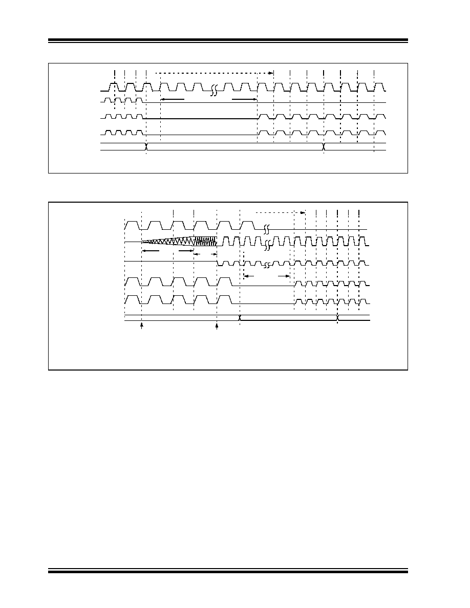
PIC18F2450/4450
DS39760A-page 36
Advance Information
� 2006 Microchip Technology Inc.
FIGURE 3-3:
TRANSITION TIMING TO RC_RUN MODE
FIGURE 3-4:
TRANSITION TIMING FROM RC_RUN MODE TO PRI_RUN MODE
Q4
Q3
Q2
OSC1
Peripheral
Program
Q1
INTRC
Q1
Counter
Clock
CPU
Clock
PC + 2
PC
1
2
3
n-1
n
Clock Transition
(1)
Q4
Q3
Q2
Q1
Q3
Q2
PC + 4
Note
1:
Clock transition typically occurs within 2-4 T
OSC
.
Q1
Q3 Q4
OSC1
Peripheral
Program
PC
INTRC
PLL Clock
Q1
PC + 4
Q2
Output
Q3
Q4
Q1
CPU Clock
PC + 2
Clock
Counter
Q2
Q2
Q3
Note
1:
T
OST
= 1024 T
OSC
; T
PLL
= 2 ms (approx). These intervals are not shown to scale.
2:
Clock transition typically occurs within 2-4 T
OSC
.
SCS1:SCS0 bits Changed
T
PLL
(1)
1
2
n-1
n
Clock
(2)
OSTS bit Set
Transition
T
OST
(1)
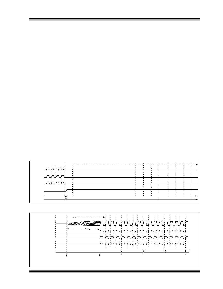
PIC18F2450/4450
� 2006 Microchip Technology Inc.
Advance Information
DS39760A-page 37
3.3
Sleep Mode
The power-managed Sleep mode in the PIC18F2450/
4450 devices is identical to the legacy Sleep mode
offered in all other PICmicro devices. It is entered by
clearing the IDLEN bit (the default state on device
Reset) and executing the SLEEP instruction. This shuts
down the selected oscillator (Figure 3-5). All clock
source status bits are cleared.
Entering the Sleep mode from any other mode does not
require a clock switch. This is because no clocks are
needed once the controller has entered Sleep. If the
WDT is selected, the INTRC source will continue to
operate. If the Timer1 oscillator is enabled, it will also
continue to run.
When a wake event occurs in Sleep mode (by interrupt,
Reset or WDT time-out), the device will not be clocked
until the clock source selected by the SCS1:SCS0 bits
becomes ready (see Figure 3-6), or it will be clocked
from the internal oscillator if either the Two-Speed
Start-up or the Fail-Safe Clock Monitor are enabled
(see Section 18.0 "Special Features of the CPU"). In
either case, the OSTS bit is set when the primary clock
is providing the device clocks. The IDLEN and SCS bits
are not affected by the wake-up.
3.4
Idle Modes
The Idle modes allow the controller's CPU to be
selectively shut down while the peripherals continue to
operate. Selecting a particular Idle mode allows users
to further manage power consumption.
If the IDLEN bit is set to `1' when a SLEEP instruction is
executed, the peripherals will be clocked from the clock
source selected using the SCS1:SCS0 bits; however, the
CPU will not be clocked. The clock source status bits are
not affected. Setting IDLEN and executing a SLEEP
instruction provides a quick method of switching from a
given Run mode to its corresponding Idle mode.
If the WDT is selected, the INTRC source will continue
to operate. If the Timer1 oscillator is enabled, it will also
continue to run.
Since the CPU is not executing instructions, the only
exits from any of the Idle modes are by interrupt, WDT
time-out or a Reset. When a wake event occurs, CPU
execution is delayed by an interval of T
CSD
(parameter 38, Table 21-10) while it becomes ready to
execute code. When the CPU begins executing code,
it resumes with the same clock source for the current
Idle mode. For example, when waking from RC_IDLE
mode, the internal oscillator will clock the CPU and
peripherals (in other words, RC_RUN mode). The
IDLEN and SCS bits are not affected by the wake-up.
While in any Idle mode or Sleep mode, a WDT time-out
will result in a WDT wake-up to the Run mode currently
specified by the SCS1:SCS0 bits.
FIGURE 3-5:
TRANSITION TIMING FOR ENTRY TO SLEEP MODE
FIGURE 3-6:
TRANSITION TIMING FOR WAKE FROM SLEEP (HSPLL)
Q4
Q3
Q2
OSC1
Peripheral
Sleep
Program
Q1
Q1
Counter
Clock
CPU
Clock
PC + 2
PC
Q3 Q4 Q1 Q2
OSC1
Peripheral
Program
PC
PLL Clock
Q3 Q4
Output
CPU Clock
Q1
Q2 Q3 Q4 Q1 Q2
Clock
Counter
PC + 6
PC + 4
Q1 Q2 Q3 Q4
Wake Event
Note 1: T
OST
= 1024 T
OSC
; T
PLL
= 2 ms (approx). These intervals are not shown to scale.
T
OST
(1)
T
PLL
(1)
OSTS bit Set
PC + 2
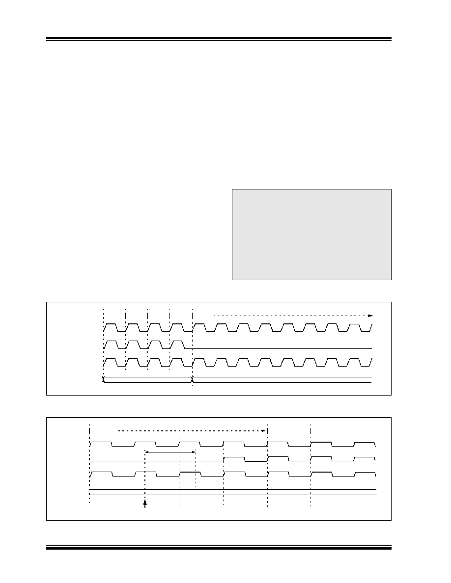
PIC18F2450/4450
DS39760A-page 38
Advance Information
� 2006 Microchip Technology Inc.
3.4.1
PRI_IDLE MODE
This mode is unique among the three low-power Idle
modes in that it does not disable the primary device
clock. For timing sensitive applications, this allows for
the fastest resumption of device operation, with its
more accurate primary clock source, since the clock
source does not have to "warm up" or transition from
another oscillator.
PRI_IDLE mode is entered from PRI_RUN mode by
setting the IDLEN bit and executing a SLEEP
instruction. If the device is in another Run mode, set
IDLEN first, then clear the SCS bits and execute
SLEEP
. Although the CPU is disabled, the peripherals
continue to be clocked from the primary clock source
specified by the FOSC3:FOSC0 Configuration bits.
The OSTS bit remains set (see Figure 3-7).
When a wake event occurs, the CPU is clocked from the
primary clock source. A delay of interval T
CSD
is
required between the wake event and when code
execution starts. This is required to allow the CPU to
become ready to execute instructions. After the wake-
up, the OSTS bit remains set. The IDLEN and SCS bits
are not affected by the wake-up (see Figure 3-8).
3.4.2
SEC_IDLE MODE
In SEC_IDLE mode, the CPU is disabled but the
peripherals continue to be clocked from the Timer1
oscillator. This mode is entered from SEC_RUN by
setting the IDLEN bit and executing a SLEEP
instruction. If the device is in another Run mode, set
IDLEN first, then set SCS1:SCS0 to `01' and execute
SLEEP
. When the clock source is switched to the
Timer1 oscillator, the primary oscillator is shut down,
the OSTS bit is cleared and the T1RUN bit is set.
When a wake event occurs, the peripherals continue to
be clocked from the Timer1 oscillator. After an interval of
T
CSD
following the wake event, the CPU begins execut-
ing code being clocked by the Timer1 oscillator. The
IDLEN and SCS bits are not affected by the wake-up;
the Timer1 oscillator continues to run (see Figure 3-8).
FIGURE 3-7:
TRANSITION TIMING FOR ENTRY TO IDLE MODE
FIGURE 3-8:
TRANSITION TIMING FOR WAKE FROM IDLE TO RUN MODE
Note:
The Timer1 oscillator should already be
running prior to entering SEC_IDLE mode.
If the T1OSCEN bit is not set when the
SLEEP
instruction is executed, the SLEEP
instruction will be ignored and entry to
SEC_IDLE mode will not occur. If the
Timer1 oscillator is enabled but not yet run-
ning, peripheral clocks will be delayed until
the oscillator has started. In such situations,
initial oscillator operation is far from stable
and unpredictable operation may result.
Q1
Peripheral
Program
PC
PC + 2
OSC1
Q3
Q4
Q1
CPU Clock
Clock
Counter
Q2
OSC1
Peripheral
Program
PC
CPU Clock
Q1
Q3
Q4
Clock
Counter
Q2
Wake Event
T
CSD

PIC18F2450/4450
� 2006 Microchip Technology Inc.
Advance Information
DS39760A-page 39
3.4.3
RC_IDLE MODE
In RC_IDLE mode, the CPU is disabled but the periph-
erals continue to be clocked from the internal oscillator,
INTRC. This mode allows for controllable power
conservation during Idle periods.
From RC_RUN, this mode is entered by setting the
IDLEN bit and executing a SLEEP instruction. If the
device is in another Run mode, first set IDLEN, then set
the SCS1 bit and execute SLEEP. Although its value is
ignored, it is recommended that SCS0 also be cleared;
this is to maintain software compatibility with future
devices. When the clock source is switched to the
INTRC, the primary oscillator is shut down and the
OSTS bit is cleared.
When a wake event occurs, the peripherals continue to
be clocked from the INTRC. After a delay of T
CSD
fol-
lowing the wake event, the CPU begins executing code
being clocked by the INTRC. The IDLEN and SCS bits
are not affected by the wake-up. The INTRC source will
continue to run if either the WDT or the Fail-Safe Clock
Monitor is enabled.
3.5
Exiting Idle and Sleep Modes
An exit from Sleep mode or any of the Idle modes is
triggered by an interrupt, a Reset or a WDT time-out.
This section discusses the triggers that cause exits
from power-managed modes. The clocking subsystem
actions are discussed in each of the power-managed
modes (see Section 3.2 "Run Modes", Section 3.3
"Sleep Mode" and Section 3.4 "Idle Modes").
3.5.1
EXIT BY INTERRUPT
Any of the available interrupt sources can cause the
device to exit from an Idle mode, or the Sleep mode, to
a Run mode. To enable this functionality, an interrupt
source must be enabled by setting its enable bit in one
of the INTCON or PIE registers. The exit sequence is
initiated when the corresponding interrupt flag bit is set.
On all exits from Idle or Sleep modes by interrupt, code
execution branches to the interrupt vector if the GIE/
GIEH bit (INTCON<7>) is set. Otherwise, code execution
continues or resumes without branching (see
Section 8.0 "Interrupts").
A fixed delay of interval T
CSD
, following the wake event,
is required when leaving Sleep and Idle modes. This
delay is required for the CPU to prepare for execution.
Instruction execution resumes on the first clock cycle
following this delay.
3.5.2
EXIT BY WDT TIME-OUT
A WDT time-out will cause different actions depending
on which power-managed mode the device is in when
the time-out occurs.
If the device is not executing code (all Idle modes and
Sleep mode), the time-out will result in an exit from the
power-managed mode (see Section 3.2 "Run
Modes" and Section 3.3 "Sleep Mode"). If the device
is executing code (all Run modes), the time-out will
result in a WDT Reset (see Section 18.2 "Watchdog
Timer (WDT)").
3.5.3
EXIT BY RESET
Normally, the device is held in Reset by the Oscillator
Start-up Timer (OST) until the primary clock becomes
ready. At that time, the OSTS bit is set and the device
begins executing code.
The exit delay time from Reset to the start of code
execution depends on both the clock sources before
and after the wake-up and the type of oscillator if the
new clock source is the primary clock. Exit delays are
summarized in Table 3-2.
Code execution can begin before the primary clock
becomes ready. If either the Two-Speed Start-up (see
Section 18.3 "Two-Speed Start-up") or Fail-Safe
Clock Monitor (see Section 18.4 "Fail-Safe Clock
Monitor") is enabled, the device may begin execution
as soon as the Reset source has cleared. Execution is
clocked by the INTRC driven by the internal oscillator.
Execution is clocked by the internal oscillator until
either the primary clock becomes ready or a power-
managed mode is entered before the primary clock
becomes ready; the primary clock is then shut down.

PIC18F2450/4450
DS39760A-page 40
Advance Information
� 2006 Microchip Technology Inc.
3.5.4
EXIT WITHOUT AN OSCILLATOR
START-UP DELAY
Certain exits from power-managed modes do not
invoke the OST at all. There are two cases:
� PRI_IDLE mode, where the primary clock source
is not stopped; and
� the primary clock source is not any of the XT or
HS modes.
In these instances, the primary clock source either
does not require an oscillator start-up delay, since it is
already running (PRI_IDLE), or normally does not
require an oscillator start-up delay (EC and any internal
oscillator modes). However, a fixed delay of interval
T
CSD
following the wake event is still required when
leaving Sleep and Idle modes to allow the CPU to
prepare for execution. Instruction execution resumes
on the first clock cycle following this delay.
TABLE 3-2:
EXIT DELAY ON WAKE-UP BY RESET FROM SLEEP MODE OR ANY IDLE MODE
(BY CLOCK SOURCES)
Microcontroller Clock Source
Exit Delay
Clock Ready Status
Bit (OSCCON)
Before Wake-up
After Wake-up
Primary Device Clock
(PRI_IDLE mode)
XT, HS
None
OSTS
XTPLL, HSPLL
EC
INTRC
(1)
T1OSC or INTRC
(1)
XT, HS
T
OST
(3)
OSTS
XTPLL, HSPLL
T
OST
+ t
rc
(3)
EC
T
CSD
(2)
INTRC
(1)
T
IOBST
(4)
INTRC
(1)
XT, HS
T
OST
(3)
OSTS
XTPLL, HSPLL
T
OST
+ t
rc
(3)
EC
T
CSD
(2)
INTRC
(1)
None
None
(Sleep mode)
XT, HS
T
OST
(3)
OSTS
XTPLL, HSPLL
T
OST
+ t
rc
(3)
EC
T
CSD
(2)
INTRC
(1)
T
IOBST
(4)
Note 1:
In this instance, refers specifically to the 31 kHz INTRC clock source.
2:
T
CSD
(parameter 38, Table 21-10) is a required delay when waking from Sleep and all Idle modes and runs
concurrently with any other required delays (see Section 3.4 "Idle Modes").
3:
T
OST
is the Oscillator Start-up Timer period (parameter 32, Table 21-10). t
rc
is the PLL lock time-out
(parameter F12, Table 21-7); it is also designated as T
PLL
.
4:
Execution continues during T
IOBST
(parameter 39, Table 21-10), the INTRC stabilization period.
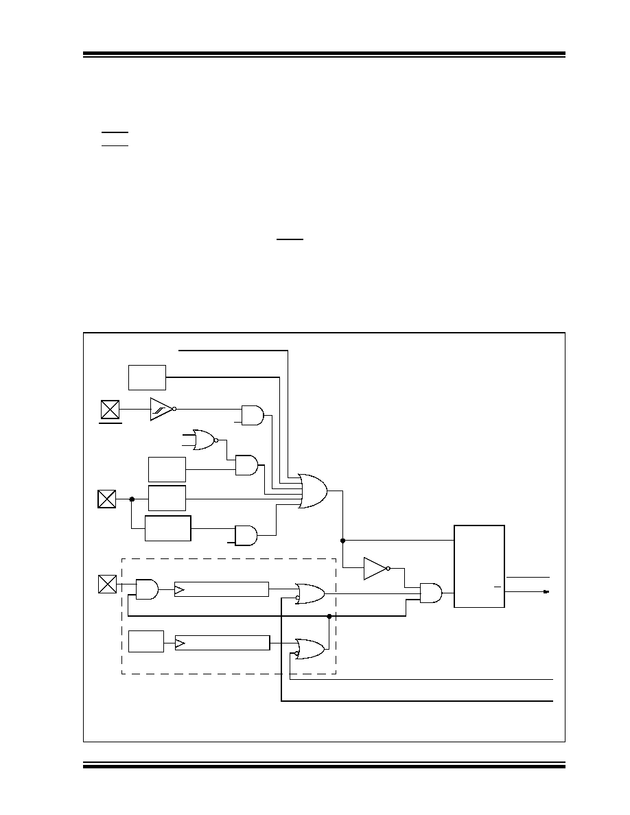
PIC18F2450/4450
� 2006 Microchip Technology Inc.
Advance Information
DS39760A-page 41
4.0
RESET
The PIC18F2450/4450 devices differentiate between
various kinds of Reset:
a)
Power-on Reset (POR)
b)
MCLR Reset during normal operation
c)
MCLR Reset during power-managed modes
d)
Watchdog Timer (WDT) Reset (during
execution)
e)
Programmable Brown-out Reset (BOR)
f)
RESET
Instruction
g)
Stack Full Reset
h)
Stack Underflow Reset
This section discusses Resets generated by MCLR,
POR and BOR and covers the operation of the various
start-up timers. Stack Reset events are covered in
Section 5.1.2.4 "Stack Full and Underflow Resets".
WDT Resets are covered in Section 18.2 "Watchdog
Timer (WDT)".
A simplified block diagram of the on-chip Reset circuit
is shown in Figure 4-1.
4.1
RCON Register
Device Reset events are tracked through the RCON
register (Register 4-1). The lower five bits of the
register indicate that a specific Reset event has
occurred. In most cases, these bits can only be cleared
by the event and must be set by the application after
the event. The state of these flag bits, taken together,
can be read to indicate the type of Reset that just
occurred. This is described in more detail in
Section 4.6 "Reset State of Registers".
The RCON register also has control bits for setting
interrupt priority (IPEN) and software control of the
BOR (SBOREN). Interrupt priority is discussed in
Section 8.0 "Interrupts". BOR is covered in
Section 4.4 "Brown-out Reset (BOR)".
FIGURE 4-1:
SIMPLIFIED BLOCK DIAGRAM OF ON-CHIP RESET CIRCUIT
S
R
Q
External Reset
MCLR
V
DD
OSC1
WDT
Time-out
V
DD
Rise
Detect
OST/PWRT
INTRC
(1)
POR Pulse
OST
10-bit Ripple Counter
PWRT
Chip_Reset
11-bit Ripple Counter
Enable OST
(2)
Enable PWRT
Note 1:
This is the INTRC source from the internal oscillator and is separate from the RC oscillator of the CLKI pin.
2:
See Table 4-2 for time-out situations.
Brown-out
Reset
BOREN
RESET
Instruction
Stack
Pointer
Stack Full/Underflow Reset
Sleep
( )_IDLE
1024 Cycles
65.5 ms
32
s
MCLRE
PIC18F2450/4450
DS39760A-page 42
Advance Information
� 2006 Microchip Technology Inc.
REGISTER 4-1:
RCON: RESET CONTROL REGISTER
R/W-0
R/W-1
(1)
U-0
R/W-1
R-1
R-1
R/W-0
(2)
R/W-0
IPEN
SBOREN
--
RI
TO
PD
POR
BOR
bit 7
bit 0
Legend:
R = Readable bit
W = Writable bit
U = Unimplemented bit, read as `0'
-n = Value at POR
`1' = Bit is set
`0' = Bit is cleared
x = Bit is unknown
bit 7
IPEN: Interrupt Priority Enable bit
1
= Enable priority levels on interrupts
0
= Disable priority levels on interrupts (PIC16CXXX Compatibility mode)
bit 6
SBOREN: BOR Software Enable bit
(1)
If BOREN1:BOREN0 = 01:
1
= BOR is enabled
0
= BOR is disabled
If BOREN1:BOREN0 = 00, 10 or 11:
Bit is disabled and read as `0'.
bit 5
Unimplemented: Read as `0'
bit 4
RI: RESET Instruction Flag bit
1
= The RESET instruction was not executed (set by firmware only)
0
= The RESET instruction was executed causing a device Reset (must be set in software after a
Brown-out Reset occurs)
bit 3
TO: Watchdog Time-out Flag bit
1
= Set by power-up, CLRWDT instruction or SLEEP instruction
0
= A WDT time-out occurred
bit 2
PD: Power-Down Detection Flag bit
1
= Set by power-up or by the CLRWDT instruction
0
= Set by execution of the SLEEP instruction
bit 1
POR: Power-on Reset Status bit
(2)
1
= A Power-on Reset has not occurred (set by firmware only)
0
= A Power-on Reset occurred (must be set in software after a Power-on Reset occurs)
bit 0
BOR: Brown-out Reset Status bit
1
= A Brown-out Reset has not occurred (set by firmware only)
0
= A Brown-out Reset occurred (must be set in software after a Brown-out Reset occurs)
Note 1:
If SBOREN is enabled, its Reset state is `1'; otherwise, it is `0'.
2:
The actual Reset value of POR is determined by the type of device Reset. See the notes following this
register and Section 4.6 "Reset State of Registers" for additional information.
Note 1: It is recommended that the POR bit be set after a Power-on Reset has been detected so that subsequent
Power-on Resets may be detected.
2: Brown-out Reset is said to have occurred when BOR is `0' and POR is `1' (assuming that POR was set to
`1' by software immediately after POR).
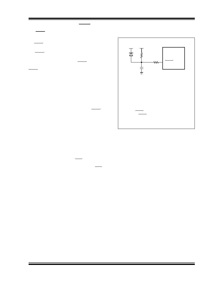
PIC18F2450/4450
� 2006 Microchip Technology Inc.
Advance Information
DS39760A-page 43
4.2
Master Clear Reset (MCLR)
The MCLR pin provides a method for triggering an
external Reset of the device. A Reset is generated by
holding the pin low. These devices have a noise filter in
the MCLR Reset path which detects and ignores small
pulses.
The MCLR pin is not driven low by any internal Resets,
including the WDT.
In PIC18F2450/4450 devices, the MCLR input can be
disabled with the MCLRE Configuration bit. When
MCLR is disabled, the pin becomes a digital input. See
Section 9.5 "PORTE, TRISE and LATE Registers"
for more information.
4.3
Power-on Reset (POR)
A Power-on Reset pulse is generated on-chip
whenever V
DD
rises above a certain threshold. This
allows the device to start in the initialized state when
V
DD
is adequate for operation.
To take advantage of the POR circuitry, tie the MCLR pin
through a resistor (1 k
to 10 k) to V
DD
. This will
eliminate external RC components usually needed to
create a Power-on Reset delay. A minimum rise rate for
V
DD
is specified (parameter D004, Section267 "DC
Characteristics"). For a slow rise time, see Figure 4-2.
When the device starts normal operation (i.e., exits the
Reset condition), device operating parameters (volt-
age, frequency, temperature, etc.) must be met to
ensure operation. If these conditions are not met, the
device must be held in Reset until the operating
conditions are met.
POR events are captured by the POR bit (RCON<1>).
The state of the bit is set to `0' whenever a POR occurs;
it does not change for any other Reset event. POR is
not reset to `1' by any hardware event. To capture
multiple events, the user manually resets the bit to `1'
in software following any POR.
FIGURE 4-2:
EXTERNAL POWER-ON
RESET CIRCUIT (FOR
SLOW V
DD
POWER-UP)
Note 1:
External Power-on Reset circuit is required
only if the V
DD
power-up slope is too slow.
The diode D helps discharge the capacitor
quickly when V
DD
powers down.
2:
R < 40 k
is recommended to make sure that
the voltage drop across R does not violate
the device's electrical specification.
3:
R1
1 k will limit any current flowing into
MCLR from external capacitor C, in the event
of MCLR/V
PP
pin breakdown, due to Electro-
static Discharge (ESD) or Electrical
Overstress (EOS).
C
R1
R
D
V
DD
MCLR
PIC18FXXXX
V
DD
PIC18F2450/4450
DS39760A-page 44
Advance Information
� 2006 Microchip Technology Inc.
4.4
Brown-out Reset (BOR)
PIC18F2450/4450 devices implement a BOR circuit
that provides the user with a number of configuration
and power-saving options. The BOR is controlled by
the BORV1:BORV0 and BOREN1:BOREN0
Configuration bits. There are a total of four BOR
configurations which are summarized in Table 4-1.
The BOR threshold is set by the BORV1:BORV0 bits. If
BOR is enabled (any values of BOREN1:BOREN0
except `00'), any drop of V
DD
below V
BOR
(parameter
D005, Section 267 "DC Characteristics: Supply
Voltage") for greater than T
BOR
(parameter 35,
Table 21-10) will reset the device. A Reset may or may
not occur if V
DD
falls below V
BOR
for less than T
BOR
.
The chip will remain in Brown-out Reset until V
DD
rises
above V
BOR
.
If the Power-up Timer is enabled, it will be invoked after
V
DD
rises above V
BOR
; it then will keep the chip in
Reset for an additional time delay, T
PWRT
(parameter 33, Table 21-10). If V
DD
drops below V
BOR
while the Power-up Timer is running, the chip will go
back into a Brown-out Reset and the Power-up Timer
will be initialized. Once V
DD
rises above V
BOR
, the
Power-up Timer will execute the additional time delay.
BOR and the Power-on Timer (PWRT) are
independently configured. Enabling BOR Reset does
not automatically enable the PWRT.
4.4.1
SOFTWARE ENABLED BOR
When BOREN1:BOREN0 = 01, the BOR can be
enabled or disabled by the user in software. This is
done with the control bit, SBOREN (RCON<6>).
Setting SBOREN enables the BOR to function as
previously described. Clearing SBOREN disables the
BOR entirely. The SBOREN bit operates only in this
mode; otherwise, it is read as `0'.
Placing the BOR under software control gives the user
the additional flexibility of tailoring the application to its
environment without having to reprogram the device to
change BOR configuration. It also allows the user to
tailor device power consumption in software by eliminat-
ing the incremental current that the BOR consumes.
While the BOR current is typically very small, it may have
some impact in low-power applications.
4.4.2
DETECTING BOR
When BOR is enabled, the BOR bit always resets to `0'
on any BOR or POR event. This makes it difficult to
determine if a BOR event has occurred just by reading
the state of BOR alone. A more reliable method is to
simultaneously check the state of both POR and BOR.
This assumes that the POR bit is reset to `1' in software
immediately after any POR event. IF BOR is `0' while
POR is `1', it can be reliably assumed that a BOR event
has occurred.
4.4.3
DISABLING BOR IN SLEEP MODE
When BOREN1:BOREN0 = 10, the BOR remains
under hardware control and operates as previously
described. Whenever the device enters Sleep mode,
however, the BOR is automatically disabled. When the
device returns to any other operating mode, BOR is
automatically re-enabled.
This mode allows for applications to recover from
brown-out situations, while actively executing code,
when the device requires BOR protection the most. At
the same time, it saves additional power in Sleep mode
by eliminating the small incremental BOR current.
TABLE 4-1:
BOR CONFIGURATIONS
Note:
Even when BOR is under software control,
the BOR Reset voltage level is still set by
the BORV1:BORV0 Configuration bits. It
cannot be changed in software.
BOR Configuration
Status of
SBOREN
(RCON<6>)
BOR Operation
BOREN1
BOREN0
0
0
Unavailable
BOR disabled; must be enabled by reprogramming the Configuration bits.
0
1
Available
BOR enabled in software; operation controlled by SBOREN.
1
0
Unavailable
BOR enabled in hardware in Run and Idle modes, disabled during
Sleep mode.
1
1
Unavailable
BOR enabled in hardware; must be disabled by reprogramming the
Configuration bits.

PIC18F2450/4450
� 2006 Microchip Technology Inc.
Advance Information
DS39760A-page 45
4.5
Device Reset Timers
PIC18F2450/4450 devices incorporate three separate
on-chip timers that help regulate the Power-on Reset
process. Their main function is to ensure that the
device clock is stable before code is executed. These
timers are:
� Power-up Timer (PWRT)
� Oscillator Start-up Timer (OST)
� PLL Lock Time-out
4.5.1
POWER-UP TIMER (PWRT)
The Power-up Timer (PWRT) of the PIC18F2450/4450
devices is an 11-bit counter which uses the INTRC
source as the clock input. This yields an approximate
time interval of 2048 x 32
s = 65.6 ms. While the
PWRT is counting, the device is held in Reset.
The power-up time delay depends on the INTRC clock
and will vary from chip to chip due to temperature and
process variation. See DC parameter 33 (Table 21-10)
for details.
The PWRT is enabled by clearing the PWRTEN
Configuration bit.
4.5.2
OSCILLATOR START-UP
TIMER (OST)
The Oscillator Start-up Timer (OST) provides a
1024 oscillator cycle (from OSC1 input) delay after the
PWRT delay is over (parameter 33, Table 21-10). This
ensures that the crystal oscillator or resonator has
started and stabilized.
The OST time-out is invoked only for XT, HS and
HSPLL modes and only on Power-on Reset or on exit
from most power-managed modes.
4.5.3
PLL LOCK TIME-OUT
With the PLL enabled in its PLL mode, the time-out
sequence following a Power-on Reset is slightly differ-
ent from other oscillator modes. A separate timer is
used to provide a fixed time-out that is sufficient for the
PLL to lock to the main oscillator frequency. This PLL
lock time-out (T
PLL
) is typically 2 ms and follows the
oscillator start-up time-out.
4.5.4
TIME-OUT SEQUENCE
On power-up, the time-out sequence is as follows:
1.
After the POR condition has cleared, PWRT
time-out is invoked (if enabled).
2.
Then, the OST is activated.
The total time-out will vary based on oscillator configu-
ration and the status of the PWRT. Figure 4-3,
Figure 4-4, Figure 4-5, Figure 4-6 and Figure 4-7 all
depict time-out sequences on power-up, with the
Power-up Timer enabled and the device operating in
HS Oscillator mode. Figure 4-3 through Figure 4-6 also
apply to devices operating in XT mode. For devices in
RC mode and with the PWRT disabled, on the other
hand, there will be no time-out at all.
Since the time-outs occur from the POR pulse, if MCLR
is kept low long enough, all time-outs will expire.
Bringing MCLR high will begin execution immediately
(Figure 4-5). This is useful for testing purposes or to
synchronize more than one PIC18FXXXX device
operating in parallel.
TABLE 4-2:
TIME-OUT IN VARIOUS SITUATIONS
Oscillator
Configuration
Power-up
(2)
and Brown-out
Exit from
Power-Managed Mode
PWRTEN = 0
PWRTEN = 1
HS, XT
66 ms
(1)
+ 1024 T
OSC
1024 T
OSC
1024 T
OSC
HSPLL, XTPLL
66 ms
(1)
+ 1024 T
OSC
+ 2 ms
(2)
1024 T
OSC
+ 2 ms
(2)
1024 T
OSC
+ 2 ms
(2)
EC, ECIO
66 ms
(1)
--
--
ECPLL, ECPIO
66 ms
(1)
+ 2 ms
(2)
2 ms
(2)
2 ms
(2)
INTIO, INTCKO
66 ms
(1)
--
--
INTHS, INTXT
66 ms
(1)
+ 1024 T
OSC
1024 T
OSC
1024 T
OSC
Note 1:
66 ms (65.5 ms) is the nominal Power-up Timer (PWRT) delay.
2:
2 ms is the nominal time required for the PLL to lock.
PIC18F2450/4450
DS39760A-page 46
Advance Information
� 2006 Microchip Technology Inc.
FIGURE 4-3:
TIME-OUT SEQUENCE ON POWER-UP (MCLR TIED TO V
DD
, V
DD
RISE < T
PWRT
)
FIGURE 4-4:
TIME-OUT SEQUENCE ON POWER-UP (MCLR NOT TIED TO V
DD
): CASE 1
FIGURE 4-5:
TIME-OUT SEQUENCE ON POWER-UP (MCLR NOT TIED TO V
DD
): CASE 2
T
PWRT
T
OST
V
DD
MCLR
INTERNAL POR
PWRT TIME-OUT
OST TIME-OUT
INTERNAL RESET
T
PWRT
T
OST
V
DD
MCLR
INTERNAL POR
PWRT TIME-OUT
OST TIME-OUT
INTERNAL RESET
V
DD
MCLR
INTERNAL POR
PWRT TIME-OUT
OST TIME-OUT
INTERNAL RESET
T
PWRT
T
OST
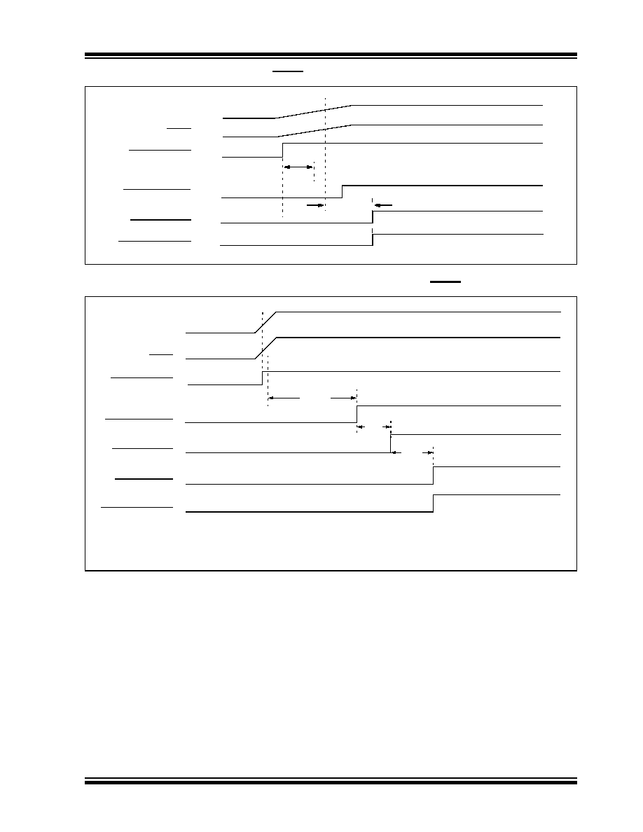
PIC18F2450/4450
� 2006 Microchip Technology Inc.
Advance Information
DS39760A-page 47
FIGURE 4-6:
SLOW RISE TIME (MCLR TIED TO V
DD
, V
DD
RISE > T
PWRT
)
FIGURE 4-7:
TIME-OUT SEQUENCE ON POR w/PLL ENABLED (MCLR TIED TO V
DD
)
V
DD
MCLR
INTERNAL POR
PWRT TIME-OUT
OST TIME-OUT
INTERNAL RESET
0V
1V
5V
T
PWRT
T
OST
T
PWRT
T
OST
V
DD
MCLR
INTERNAL POR
PWRT TIME-OUT
OST TIME-OUT
INTERNAL RESET
PLL TIME-OUT
T
PLL
Note:
T
OST
= 1024 clock cycles.
T
PLL
2 ms max. First three stages of the Power-up Timer.
PIC18F2450/4450
DS39760A-page 48
Advance Information
� 2006 Microchip Technology Inc.
4.6
Reset State of Registers
Most registers are unaffected by a Reset. Their status
is unknown on POR and unchanged by all other
Resets. The other registers are forced to a "Reset
state" depending on the type of Reset that occurred.
Most registers are not affected by a WDT wake-up,
since this is viewed as the resumption of normal oper-
ation. Status bits from the RCON register, RI, TO, PD,
POR and BOR, are set or cleared differently in different
Reset situations as indicated in Table 4-3. These bits
are used in software to determine the nature of the
Reset.
Table 4-4 describes the Reset states for all of the
Special Function Registers. These are categorized by
Power-on and Brown-out Resets, Master Clear and
WDT Resets and WDT wake-ups.
TABLE 4-3:
STATUS BITS, THEIR SIGNIFICANCE AND THE INITIALIZATION CONDITION
FOR RCON REGISTER
Condition
Program
Counter
RCON Register
STKPTR Register
SBOREN
RI
TO
PD
POR BOR STKFUL STKUNF
Power-on Reset
0000h
1
1
1
1
0
0
0
0
RESET
Instruction
0000h
u
(2)
0
u
u
u
u
u
u
Brown-out
0000h
u
(2)
1
1
1
u
0
u
u
MCLR during Power-Managed
Run modes
0000h
u
(2)
u
1
u
u
u
u
u
MCLR during Power-Managed
Idle modes and Sleep mode
0000h
u
(2)
u
1
0
u
u
u
u
WDT Time-out during Full Power or
Power-Managed Run modes
0000h
u
(2)
u
0
u
u
u
u
u
MCLR during Full Power Execution
0000h
u
(2)
u
u
u
u
u
u
u
Stack Full Reset (STVREN = 1)
0000h
u
(2)
u
u
u
u
u
1
u
Stack Underflow Reset
(STVREN = 1)
0000h
u
(2)
u
u
u
u
u
u
1
Stack Underflow Error (not an actual
Reset, STVREN = 0)
0000h
u
(2)
u
u
u
u
u
u
1
WDT Time-out during Power-Managed
Idle or Sleep modes
PC + 2
u
(2)
u
0
0
u
u
u
u
Interrupt Exit from
Power-Managed modes
PC + 2
(1)
u
(2)
u
u
0
u
u
u
u
Legend: u = unchanged
Note 1:
When the wake-up is due to an interrupt and the GIEH or GIEL bits are set, the PC is loaded with the
interrupt vector (008h or 0018h).
2:
Reset state is `1' for POR and unchanged for all other Resets when software BOR is enabled
(BOREN1:BOREN0 Configuration bits = 01 and SBOREN = 1); otherwise, the Reset state is `0'.

PIC18F2450/4450
� 2006 Microchip Technology Inc.
Advance Information
DS39760A-page 49
TABLE 4-4:
INITIALIZATION CONDITIONS FOR ALL REGISTERS
Register
Applicable Devices
Power-on Reset,
Brown-out Reset
MCLR Resets,
WDT Reset,
RESET
Instruction,
Stack Resets
Wake-up via WDT
or Interrupt
TOSU
2450
4450
---0 0000
---0 0000
---0 uuuu
(1)
TOSH
2450
4450
0000 0000
0000 0000
uuuu uuuu
(1)
TOSL
2450
4450
0000 0000
0000 0000
uuuu uuuu
(1)
STKPTR
2450
4450
00-0 0000
uu-0 0000
uu-u uuuu
(1)
PCLATU
2450
4450
---0 0000
---0 0000
---u uuuu
PCLATH
2450
4450
0000 0000
0000 0000
uuuu uuuu
PCL
2450
4450
0000 0000
0000 0000
PC + 2
(3)
TBLPTRU
2450
4450
--00 0000
--00 0000
--uu uuuu
TBLPTRH
2450
4450
0000 0000
0000 0000
uuuu uuuu
TBLPTRL
2450
4450
0000 0000
0000 0000
uuuu uuuu
TABLAT
2450
4450
0000 0000
0000 0000
uuuu uuuu
PRODH
2450
4450
xxxx xxxx
uuuu uuuu
uuuu uuuu
PRODL
2450
4450
xxxx xxxx
uuuu uuuu
uuuu uuuu
INTCON
2450
4450
0000 000x
0000 000u
uuuu uuuu
(2)
INTCON2
2450
4450
1111 -1-1
1111 -1-1
uuuu -u-u
(2)
INTCON3
2450
4450
11-0 0-00
11-0 0-00
uu-u u-uu
(2)
INDF0
2450
4450
N/A
N/A
N/A
POSTINC0
2450
4450
N/A
N/A
N/A
POSTDEC0
2450
4450
N/A
N/A
N/A
PREINC0
2450
4450
N/A
N/A
N/A
PLUSW0
2450
4450
N/A
N/A
N/A
FSR0H
2450
4450
---- 0000
---- 0000
---- uuuu
FSR0L
2450
4450
xxxx xxxx
uuuu uuuu
uuuu uuuu
WREG
2450
4450
xxxx xxxx
uuuu uuuu
uuuu uuuu
INDF1
2450
4450
N/A
N/A
N/A
POSTINC1
2450
4450
N/A
N/A
N/A
POSTDEC1
2450
4450
N/A
N/A
N/A
PREINC1
2450
4450
N/A
N/A
N/A
PLUSW1
2450
4450
N/A
N/A
N/A
FSR1H
2450
4450
---- 0000
---- 0000
---- uuuu
FSR1L
2450
4450
xxxx xxxx
uuuu uuuu
uuuu uuuu
BSR
2450
4450
---- 0000
---- 0000
---- uuuu
Legend: u = unchanged, x = unknown, - = unimplemented bit, read as `0', q = value depends on condition.
Shaded cells indicate conditions do not apply for the designated device.
Note 1:
When the wake-up is due to an interrupt and the GIEL or GIEH bit is set, the TOSU, TOSH and TOSL are
updated with the current value of the PC. The STKPTR is modified to point to the next location in the
hardware stack.
2:
One or more bits in the INTCONx or PIRx registers will be affected (to cause wake-up).
3:
When the wake-up is due to an interrupt and the GIEL or GIEH bit is set, the PC is loaded with the
interrupt vector (0008h or 0018h).
4:
See Table 4-3 for Reset value for specific condition.
5:
PORTA<6>, LATA<6> and TRISA<6> are enabled depending on the oscillator mode selected. When not
enabled as PORTA pins, they are disabled and read `0'.

PIC18F2450/4450
DS39760A-page 50
Advance Information
� 2006 Microchip Technology Inc.
INDF2
2450
4450
N/A
N/A
N/A
POSTINC2
2450
4450
N/A
N/A
N/A
POSTDEC2
2450
4450
N/A
N/A
N/A
PREINC2
2450
4450
N/A
N/A
N/A
PLUSW2
2450
4450
N/A
N/A
N/A
FSR2H
2450
4450
---- 0000
---- 0000
---- uuuu
FSR2L
2450
4450
xxxx xxxx
uuuu uuuu
uuuu uuuu
STATUS
2450
4450
---x xxxx
---u uuuu
---u uuuu
TMR0H
2450
4450
0000 0000
0000 0000
uuuu uuuu
TMR0L
2450
4450
xxxx xxxx
uuuu uuuu
uuuu uuuu
T0CON
2450
4450
1111 1111
1111 1111
uuuu uuuu
OSCCON
2450
4450
0--- q-00
0--- 0-q0
u--- u-qu
HLVDCON
2450
4450
0-00 0101
0-00 0101
u-uu uuuu
WDTCON
2450
4450
---- ---0
---- ---0
---- ---u
RCON
(4)
2450
4450
0q-1 11q0
0q-q qquu
uq-u qquu
TMR1H
2450
4450
xxxx xxxx
uuuu uuuu
uuuu uuuu
TMR1L
2450
4450
xxxx xxxx
uuuu uuuu
uuuu uuuu
T1CON
2450
4450
0000 0000
u0uu uuuu
uuuu uuuu
TMR2
2450
4450
0000 0000
0000 0000
uuuu uuuu
PR2
2450
4450
1111 1111
1111 1111
1111 1111
T2CON
2450
4450
-000 0000
-000 0000
-uuu uuuu
ADRESH
2450
4450
xxxx xxxx
uuuu uuuu
uuuu uuuu
ADRESL
2450
4450
xxxx xxxx
uuuu uuuu
uuuu uuuu
ADCON0
2450
4450
--00 0000
--00 0000
--uu uuuu
ADCON1
2450
4450
--00 qqqq
--00 qqqq
--uu uuuu
ADCON2
2450
4450
0-00 0000
0-00 0000
u-uu uuuu
CCPR1H
2450
4450
xxxx xxxx
uuuu uuuu
uuuu uuuu
CCPR1L
2450
4450
xxxx xxxx
uuuu uuuu
uuuu uuuu
CCP1CON
2450
4450
--00 0000
--00 0000
--uu uuuu
SPBRG
2450
4450
0000 0000
0000 0000
uuuu uuuu
RCREG
2450
4450
0000 0000
0000 0000
uuuu uuuu
TXREG
2450
4450
0000 0000
0000 0000
uuuu uuuu
TABLE 4-4:
INITIALIZATION CONDITIONS FOR ALL REGISTERS (CONTINUED)
Register
Applicable Devices
Power-on Reset,
Brown-out Reset
MCLR Resets,
WDT Reset,
RESET
Instruction,
Stack Resets
Wake-up via WDT
or Interrupt
Legend: u = unchanged, x = unknown, - = unimplemented bit, read as `0', q = value depends on condition.
Shaded cells indicate conditions do not apply for the designated device.
Note 1:
When the wake-up is due to an interrupt and the GIEL or GIEH bit is set, the TOSU, TOSH and TOSL are
updated with the current value of the PC. The STKPTR is modified to point to the next location in the
hardware stack.
2:
One or more bits in the INTCONx or PIRx registers will be affected (to cause wake-up).
3:
When the wake-up is due to an interrupt and the GIEL or GIEH bit is set, the PC is loaded with the
interrupt vector (0008h or 0018h).
4:
See Table 4-3 for Reset value for specific condition.
5:
PORTA<6>, LATA<6> and TRISA<6> are enabled depending on the oscillator mode selected. When not
enabled as PORTA pins, they are disabled and read `0'.

PIC18F2450/4450
� 2006 Microchip Technology Inc.
Advance Information
DS39760A-page 51
TXSTA
2450
4450
0000 0010
0000 0010
uuuu uuuu
RCSTA
2450
4450
0000 000x
0000 000x
uuuu uuuu
EECON2
2450
4450
0000 0000
0000 0000
0000 0000
EECON1
2450
4450
-x-0 x00-
-u-0 u00-
-u-0 u00-
IPIR2
2450
4450
1-1- -1--
1-1- -1--
u-u- -u--
PIR2
2450
4450
0-0- -0--
0-0- -0--
u-u- -u--
(2)
PIE2
2450
4450
0-0- -0--
0-0- -0--
u-u- -u--
IPR1
2450
4450
-111 -111
-111 -111
-uuu -uuu
PIR1
2450
4450
-000 -000
-000 -000
-uuu -uuu
(2)
PIE1
2450
4450
-000 -000
-000 -000
-uuu -uuu
TRISE
2450
4450
---- -111
---- -111
uuuu -uuu
TRISD
2450
4450
1111 1111
1111 1111
uuuu uuuu
TRISC
2450
4450
11-- -111
11-- -111
uu-- -uuu
TRISB
2450
4450
1111 1111
1111 1111
uuuu uuuu
TRISA
(5)
2450
4450
-111 1111
(5)
-111 1111
(5)
-uuu uuuu
(5)
LATE
2450
4450
---- -xxx
---- -uuu
---- -uuu
LATD
2450
4450
xxxx xxxx
uuuu uuuu
uuuu uuuu
LATC
2450
4450
xx-- -xxx
uu-- -uuu
uu-- -uuu
LATB
2450
4450
xxxx xxxx
uuuu uuuu
uuuu uuuu
LATA
(5)
2450
4450
-xxx xxxx
(5)
-uuu uuuu
(5)
-uuu uuuu
(5)
PORTE
2450
4450
---- x000
---- x000
---- uuuu
PORTD
2450
4450
xxxx xxxx
uuuu uuuu
uuuu uuuu
PORTC
2450
4450
xxxx -xxx
uuuu -uuu
uuuu -uuu
PORTB
2450
4450
xxxx xxxx
uuuu uuuu
uuuu uuuu
PORTA
(5)
2450
4450
-x0x 0000
(5)
-u0u 0000
(5)
-uuu uuuu
(5)
UEP15
2450
4450
---0 0000
---0 0000
---u uuuu
UEP14
2450
4450
---0 0000
---0 0000
---u uuuu
UEP13
2450
4450
---0 0000
---0 0000
---u uuuu
UEP12
2450
4450
---0 0000
---0 0000
---u uuuu
UEP11
2450
4450
---0 0000
---0 0000
---u uuuu
UEP10
2450
4450
---0 0000
---0 0000
---u uuuu
UEP9
2450
4450
---0 0000
---0 0000
---u uuuu
TABLE 4-4:
INITIALIZATION CONDITIONS FOR ALL REGISTERS (CONTINUED)
Register
Applicable Devices
Power-on Reset,
Brown-out Reset
MCLR Resets,
WDT Reset,
RESET
Instruction,
Stack Resets
Wake-up via WDT
or Interrupt
Legend: u = unchanged, x = unknown, - = unimplemented bit, read as `0', q = value depends on condition.
Shaded cells indicate conditions do not apply for the designated device.
Note 1:
When the wake-up is due to an interrupt and the GIEL or GIEH bit is set, the TOSU, TOSH and TOSL are
updated with the current value of the PC. The STKPTR is modified to point to the next location in the
hardware stack.
2:
One or more bits in the INTCONx or PIRx registers will be affected (to cause wake-up).
3:
When the wake-up is due to an interrupt and the GIEL or GIEH bit is set, the PC is loaded with the
interrupt vector (0008h or 0018h).
4:
See Table 4-3 for Reset value for specific condition.
5:
PORTA<6>, LATA<6> and TRISA<6> are enabled depending on the oscillator mode selected. When not
enabled as PORTA pins, they are disabled and read `0'.

PIC18F2450/4450
DS39760A-page 52
Advance Information
� 2006 Microchip Technology Inc.
UEP8
2450
4450
---0 0000
---0 0000
---u uuuu
UEP7
2450
4450
---0 0000
---0 0000
---u uuuu
UEP6
2450
4450
---0 0000
---0 0000
---u uuuu
UEP5
2450
4450
---0 0000
---0 0000
---u uuuu
UEP4
2450
4450
---0 0000
---0 0000
---u uuuu
UEP3
2450
4450
---0 0000
---0 0000
---u uuuu
UEP2
2450
4450
---0 0000
---0 0000
---u uuuu
UEP1
2450
4450
---0 0000
---0 0000
---u uuuu
UEP0
2450
4450
---0 0000
---0 0000
---u uuuu
UCFG
2450
4450
00-0 0000
00-0 0000
uu-u uuuu
UADDR
2450
4450
-000 0000
-000 0000
-uuu uuuu
UCON
2450
4450
-0x0 000-
-0x0 000-
-uuu uuu-
USTAT
2450
4450
-xxx xxx-
-xxx xxx-
-uuu uuu-
UEIE
2450
4450
0--0 0000
0--0 0000
u--u uuuu
UEIR
2450
4450
0--0 0000
0--0 0000
u--u uuuu
UIE
2450
4450
-000 0000
-000 0000
-uuu uuuu
UIR
2450
4450
-000 0000
-000 0000
-uuu uuuu
UFRMH
2450
4450
---- -xxx
---- -xxx
---- -uuu
UFRML
2450
4450
xxxx xxxx
xxxx xxxx
uuuu uuuu
TABLE 4-4:
INITIALIZATION CONDITIONS FOR ALL REGISTERS (CONTINUED)
Register
Applicable Devices
Power-on Reset,
Brown-out Reset
MCLR Resets,
WDT Reset,
RESET
Instruction,
Stack Resets
Wake-up via WDT
or Interrupt
Legend: u = unchanged, x = unknown, - = unimplemented bit, read as `0', q = value depends on condition.
Shaded cells indicate conditions do not apply for the designated device.
Note 1:
When the wake-up is due to an interrupt and the GIEL or GIEH bit is set, the TOSU, TOSH and TOSL are
updated with the current value of the PC. The STKPTR is modified to point to the next location in the
hardware stack.
2:
One or more bits in the INTCONx or PIRx registers will be affected (to cause wake-up).
3:
When the wake-up is due to an interrupt and the GIEL or GIEH bit is set, the PC is loaded with the
interrupt vector (0008h or 0018h).
4:
See Table 4-3 for Reset value for specific condition.
5:
PORTA<6>, LATA<6> and TRISA<6> are enabled depending on the oscillator mode selected. When not
enabled as PORTA pins, they are disabled and read `0'.
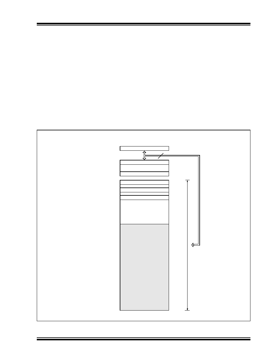
PIC18F2450/4450
� 2006 Microchip Technology Inc.
Advance Information
DS39760A-page 53
5.0
MEMORY ORGANIZATION
There are two types of memory in PIC18F2450/4450
microcontroller devices:
� Program Memory
� Data RAM
As Harvard architecture devices, the data and program
memories use separate busses; this allows for
concurrent access of the two memory spaces.
Additional detailed information on the operation of the
Flash program memory is provided in Section 6.0
"Flash Program Memory".
5.1
Program Memory Organization
PIC18 microcontrollers implement a 21-bit program
counter which is capable of addressing a 2-Mbyte
program memory space. Accessing a location between
the upper boundary of the physically implemented
memory and the 2-Mbyte address will return all `0's (a
NOP
instruction).
The PIC18F2450 and PIC18F4450 each have 16 Kbytes
of Flash memory and can store up to 8192 single-word
instructions.
PIC18 devices have two interrupt vectors. The Reset
vector address is at 0000h and the interrupt vector
addresses are at 0008h and 0018h.
The program memory maps for PIC18F2450 and
PIC18F4450 devices are shown in Figure 5-1.
FIGURE 5-1:
PROGRAM MEMORY MAP AND STACK FOR PIC18F2450/4450 DEVICES
PC<20:0>
Stack Level 1
�
Stack Level 31
Reset Vector
Low Priority Interrupt Vector
�
�
CALL, RCALL, RETURN,
RETFIE, RETLW, CALLW,
21
0000h
0018h
On-Chip
Program Memory
High Priority Interrupt Vector 0008h
User Mem
o
ry Space
1FFFFFh
4000h
3FFFh
Read `0'
200000h
PIC18F2450/4450
ADDULNK, SUBULNK

PIC18F2450/4450
DS39760A-page 54
Advance Information
� 2006 Microchip Technology Inc.
5.1.1
PROGRAM COUNTER
The Program Counter (PC) specifies the address of the
instruction to fetch for execution. The PC is 21 bits wide
and is contained in three separate 8-bit registers. The
low byte, known as the PCL register, is both readable
and writable. The high byte, or PCH register, contains
the PC<15:8> bits; it is not directly readable or writable.
Updates to the PCH register are performed through the
PCLATH register. The upper byte is called PCU. This
register contains the PC<20:16> bits; it is also not
directly readable or writable. Updates to the PCU
register are performed through the PCLATU register.
The contents of PCLATH and PCLATU are transferred
to the program counter by any operation that writes
PCL. Similarly, the upper two bytes of the program
counter are transferred to PCLATH and PCLATU by an
operation that reads PCL. This is useful for computed
offsets to the PC (see Section 5.1.4.1 "Computed
GOTO").
The PC addresses bytes in the program memory. To
prevent the PC from becoming misaligned with word
instructions, the Least Significant bit of PCL is fixed to
a value of `0'. The PC increments by 2 to address
sequential instructions in the program memory.
The CALL, RCALL and GOTO program branch
instructions write to the program counter directly. For
these instructions, the contents of PCLATH and
PCLATU are not transferred to the program counter.
5.1.2
RETURN ADDRESS STACK
The return address stack allows any combination of up
to 31 program calls and interrupts to occur. The PC is
pushed onto the stack when a CALL or RCALL
instruction is executed or an interrupt is Acknowledged.
The PC value is pulled off the stack on a RETURN,
RETLW
or a RETFIE instruction. PCLATU and PCLATH
are not affected by any of the RETURN or CALL
instructions.
The stack operates as a 31-word by 21-bit RAM and a
5-bit Stack Pointer, STKPTR. The stack space is not
part of either program or data space. The Stack Pointer
is readable and writable and the address on the top of
the stack is readable and writable through the Top-of-
Stack Special Function Registers. Data can also be
pushed to, or popped from the stack, using these
registers.
A CALL type instruction causes a push onto the stack.
The Stack Pointer is first incremented and the location
pointed to by the Stack Pointer is written with the
contents of the PC (already pointing to the instruction
following the CALL). A RETURN type instruction causes
a pop from the stack. The contents of the location
pointed to by the STKPTR are transferred to the PC
and then the Stack Pointer is decremented.
The Stack Pointer is initialized to `00000' after all
Resets. There is no RAM associated with the location
corresponding to a Stack Pointer value of `00000'; this
is only a Reset value. Status bits indicate if the stack is
full, has overflowed or has underflowed.
5.1.2.1
Top-of-Stack Access
Only the top of the return address stack (TOS) is
readable and writable. A set of three registers,
TOSU:TOSH:TOSL, hold the contents of the stack loca-
tion pointed to by the STKPTR register (Figure 5-2). This
allows users to implement a software stack if necessary.
After a CALL, RCALL or interrupt, the software can read
the pushed value by reading the TOSU:TOSH:TOSL
registers. These values can be placed on a user-defined
software stack. At return time, the software can return
these values to TOSU:TOSH:TOSL and do a return.
The user must disable the global interrupt enable bits
while accessing the stack to prevent inadvertent stack
corruption.
FIGURE 5-2:
RETURN ADDRESS STACK AND ASSOCIATED REGISTERS
00011
001A34h
11111
11110
11101
00010
00001
00000
00010
Return Address Stack<20:0>
Top-of-Stack
000D58h
TOSL
TOSH
TOSU
34h
1Ah
00h
STKPTR<4:0>
Top-of-Stack Registers
Stack Pointer
PIC18F2450/4450
� 2006 Microchip Technology Inc.
Advance Information
DS39760A-page 55
5.1.2.2
Return Stack Pointer (STKPTR)
The STKPTR register (Register 5-1) contains the Stack
Pointer value, the STKFUL (Stack Full) status bit and
the STKUNF (Stack Underflow) status bit. The value of
the Stack Pointer can be 0 through 31. The Stack
Pointer increments before values are pushed onto the
stack and decrements after values are popped off the
stack. On Reset, the Stack Pointer value will be zero.
The user may read and write the Stack Pointer value.
This feature can be used by a Real-Time Operating
System (RTOS) for return stack maintenance.
After the PC is pushed onto the stack 31 times (without
popping any values off the stack), the STKFUL bit is
set. The STKFUL bit is cleared by software or by a
POR.
The action that takes place when the stack becomes
full depends on the state of the STVREN (Stack
Overflow Reset Enable) Configuration bit. (Refer to
Section 18.1 "Configuration Bits" for a description of
the device Configuration bits.) If STVREN is set
(default), the 31st push will push the (PC + 2) value
onto the stack, set the STKFUL bit and reset the
device. The STKFUL bit will remain set and the Stack
Pointer will be set to zero.
If STVREN is cleared, the STKFUL bit will be set on the
31st push and the Stack Pointer will increment to 31.
Any additional pushes will not overwrite the 31st push
and the STKPTR will remain at 31.
When the stack has been popped enough times to
unload the stack, the next pop will return a value of zero
to the PC and sets the STKUNF bit, while the Stack
Pointer remains at zero. The STKUNF bit will remain
set until cleared by software or until a POR occurs.
5.1.2.3
PUSH
and
POP
Instructions
Since the Top-of-Stack is readable and writable, the
ability to push values onto the stack and pull values off
the stack, without disturbing normal program execu-
tion, is a desirable feature. The PIC18 instruction set
includes two instructions, PUSH and POP, that permit
the TOS to be manipulated under software control.
TOSU, TOSH and TOSL can be modified to place data
or a return address on the stack.
The PUSH instruction places the current PC value onto
the stack. This increments the Stack Pointer and loads
the current PC value onto the stack.
The POP instruction discards the current TOS by
decrementing the Stack Pointer. The previous value
pushed onto the stack then becomes the TOS value.
Note:
Returning a value of zero to the PC on an
underflow has the effect of vectoring the
program to the Reset vector, where the
stack conditions can be verified and
appropriate actions can be taken. This is
not the same as a Reset, as the contents
of the SFRs are not affected.
REGISTER 5-1:
STKPTR: STACK POINTER REGISTER
R/C-0
R/C-0
U-0
R/W-0
R/W-0
R/W-0
R/W-0
R/W-0
STKFUL
(1)
STKUNF
(1)
--
SP4
SP3
SP2
SP1
SP0
bit 7
bit 0
Legend:
C = Clearable bit
R = Readable bit
W = Writable bit
U = Unimplemented bit, read as `0'
-n = Value at POR
`1' = Bit is set
`0' = Bit is cleared
x = Bit is unknown
bit 7
STKFUL: Stack Full Flag bit
(1)
1
= Stack became full or overflowed
0
= Stack has not become full or overflowed
bit 6
STKUNF: Stack Underflow Flag bit
(1)
1
= Stack underflow occurred
0
= Stack underflow did not occur
bit 5
Unimplemented: Read as `0'
bit 4-0
SP4:SP0: Stack Pointer Location bits
Note 1:
Bit 7 and bit 6 are cleared by user software or by a POR.

PIC18F2450/4450
DS39760A-page 56
Advance Information
� 2006 Microchip Technology Inc.
5.1.2.4
Stack Full and Underflow Resets
Device Resets on stack overflow and stack underflow
conditions are enabled by setting the STVREN bit in
Configuration Register 4L. When STVREN is set, a full
or underflow condition will set the appropriate STKFUL
or STKUNF bit and then cause a device Reset. When
STVREN is cleared, a full or underflow condition will set
the appropriate STKFUL or STKUNF bit but not cause
a device Reset. The STKFUL or STKUNF bits are
cleared by user software or a Power-on Reset.
5.1.3
FAST REGISTER STACK
A Fast Register Stack is provided for the STATUS,
WREG and BSR registers to provide a "fast return"
option for interrupts. Each stack is only one level deep
and is neither readable nor writable. It is loaded with the
current value of the corresponding register when the
processor vectors for an interrupt. All interrupt sources
will push values into the stack registers. The values in
the registers are then loaded back into their associated
registers if the RETFIE, FAST instruction is used to
return from the interrupt.
If both low and high priority interrupts are enabled, the
stack registers cannot be used reliably to return from
low priority interrupts. If a high priority interrupt occurs
while servicing a low priority interrupt, the stack register
values stored by the low priority interrupt will be
overwritten. In these cases, users must save the key
registers in software during a low priority interrupt.
If interrupt priority is not used, all interrupts may use the
Fast Register Stack for returns from interrupt. If no
interrupts are used, the Fast Register Stack can be
used to restore the STATUS, WREG and BSR registers
at the end of a subroutine call. To use the Fast Register
Stack for a subroutine call, a CALL label, FAST
instruction must be executed to save the STATUS,
WREG and BSR registers to the Fast Register Stack. A
RETURN,
FAST instruction is then executed to restore
these registers from the Fast Register Stack.
Example 5-1 shows a source code example that uses
the Fast Register Stack during a subroutine call and
return.
EXAMPLE 5-1:
FAST REGISTER STACK
CODE EXAMPLE
5.1.4
LOOK-UP TABLES IN PROGRAM
MEMORY
There may be programming situations that require the
creation of data structures, or look-up tables, in
program memory. For PIC18 devices, look-up tables
can be implemented in two ways:
� Computed GOTO
� Table Reads
5.1.4.1
Computed GOTO
A computed GOTO is accomplished by adding an offset
to the program counter. An example is shown in
Example 5-2.
A look-up table can be formed with an ADDWF PCL
instruction and a group of RETLW nn instructions. The
W register is loaded with an offset into the table before
executing a call to that table. The first instruction of the
called routine is the ADDWF PCL instruction. The next
instruction executed will be one of the RETLW nn
instructions that returns the value `nn' to the calling
function.
The offset value (in WREG) specifies the number of
bytes that the program counter should advance and
should be multiples of 2 (LSb = 0).
In this method, only one data byte may be stored in
each instruction location and room on the return
address stack is required.
EXAMPLE 5-2:
COMPUTED GOTO USING
AN OFFSET VALUE
5.1.4.2
Table Reads and Table Writes
A better method of storing data in program memory
allows two bytes of data to be stored in each instruction
location.
Look-up table data may be stored two bytes per
program word by using table reads and writes. The
Table Pointer (TBLPTR) register specifies the byte
address and the Table Latch (TABLAT) register
contains the data that is read from or written to program
memory. Data is transferred to or from program
memory one byte at a time.
Table read and table write operations are discussed
further in Section 6.1 "Table Reads and Table
Writes".
CALL
SUB1, FAST
;STATUS, WREG, BSR
;SAVED IN FAST REGISTER
;STACK
�
�
SUB1
�
�
RETURN, FAST
;RESTORE VALUES SAVED
;IN FAST REGISTER STACK
MOVF
OFFSET, W
CALL
TABLE
ORG nn00h
TABLE
ADDWF
PCL
RETLW
nnh
RETLW
nnh
RETLW
nnh
.
.
.
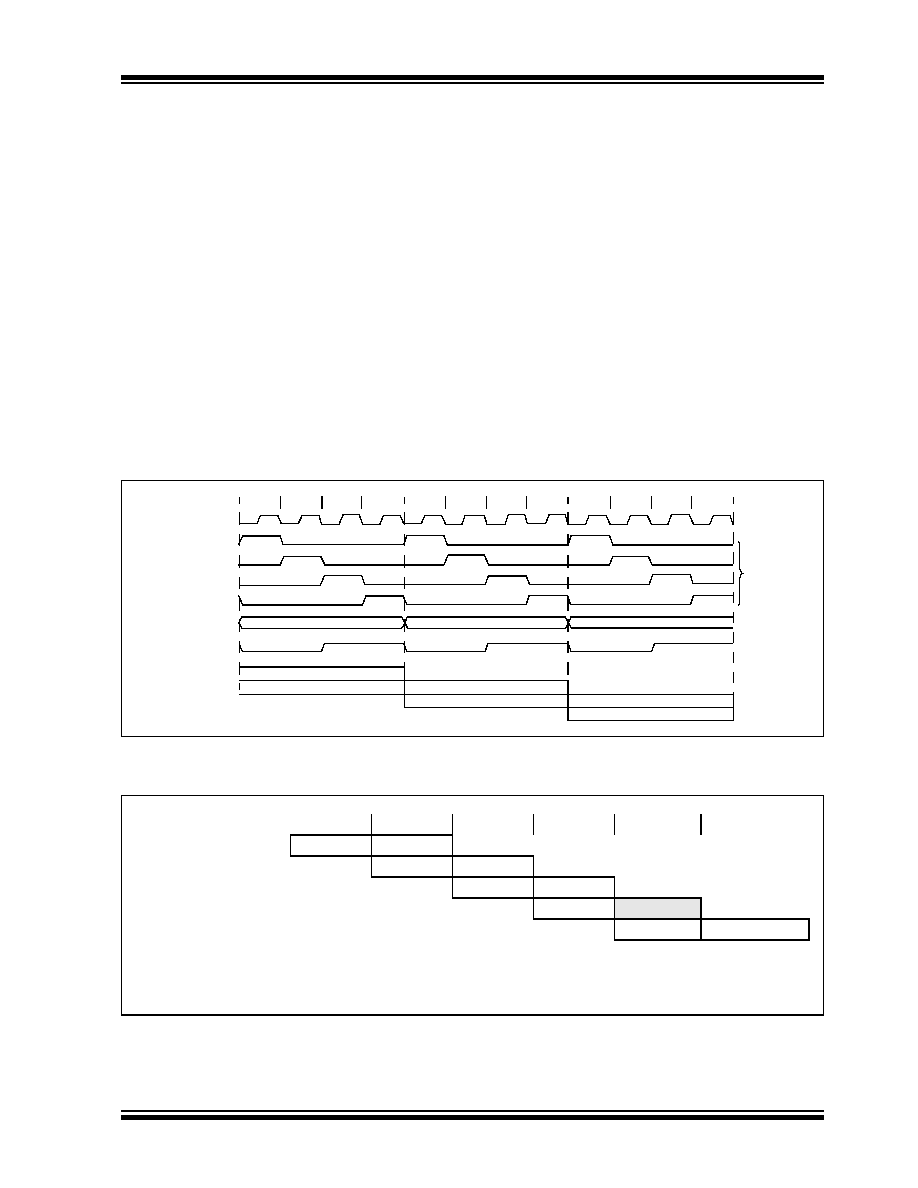
PIC18F2450/4450
� 2006 Microchip Technology Inc.
Advance Information
DS39760A-page 57
5.2
PIC18 Instruction Cycle
5.2.1
CLOCKING SCHEME
The microcontroller clock input, whether from an
internal or external source, is internally divided by four
to generate four non-overlapping quadrature clocks
(Q1, Q2, Q3 and Q4). Internally, the program counter is
incremented on every Q1; the instruction is fetched
from the program memory and latched into the Instruc-
tion Register (IR) during Q4. The instruction is decoded
and executed during the following Q1 through Q4. The
clocks and instruction execution flow are shown in
Figure 5-3.
5.2.2
INSTRUCTION FLOW/PIPELINING
An "Instruction Cycle" consists of four Q cycles: Q1
through Q4. The instruction fetch and execute are
pipelined in such a manner that a fetch takes one
instruction cycle, while the decode and execute takes
another instruction cycle. However, due to the
pipelining, each instruction effectively executes in one
cycle. If an instruction causes the program counter to
change (e.g., GOTO), then two cycles are required to
complete the instruction (Example 5-3).
A fetch cycle begins with the Program Counter (PC)
incrementing in Q1.
In the execution cycle, the fetched instruction is latched
into the Instruction Register (IR) in cycle Q1. This
instruction is then decoded and executed during the
Q2, Q3 and Q4 cycles. Data memory is read during Q2
(operand read) and written during Q4 (destination
write).
FIGURE 5-3:
CLOCK/INSTRUCTION CYCLE
EXAMPLE 5-3:
INSTRUCTION PIPELINE FLOW
Q1
Q2
Q3
Q4
Q1
Q2
Q3
Q4
Q1
Q2
Q3
Q4
OSC1
Q1
Q2
Q3
Q4
PC
OSC2/CLKO
(RC mode)
PC
PC + 2
PC + 4
Fetch INST (PC)
Execute INST (PC � 2)
Fetch INST (PC + 2)
Execute INST (PC)
Fetch INST (PC + 4)
Execute INST (PC + 2)
Internal
Phase
Clock
Note:
All instructions are single cycle, except for any program branches. These take two cycles since the fetch
instruction is "flushed" from the pipeline while the new instruction is being fetched and then executed.
T
CY
0
T
CY
1
T
CY
2
T
CY
3
T
CY
4
T
CY
5
1. MOVLW 55h
Fetch 1
Execute 1
2. MOVWF PORTB
Fetch 2
Execute 2
3. BRA SUB_1
Fetch 3
Execute 3
4. BSF PORTA, BIT3 (Forced NOP)
Fetch 4
Flush (NOP)
5. Instruction @ address SUB_1
Fetch SUB_1 Execute SUB_1
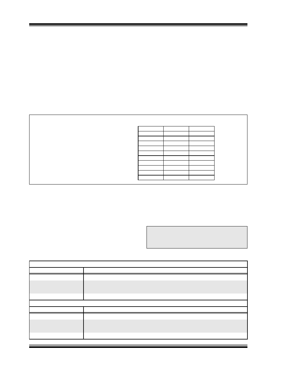
PIC18F2450/4450
DS39760A-page 58
Advance Information
� 2006 Microchip Technology Inc.
5.2.3
INSTRUCTIONS IN PROGRAM
MEMORY
The program memory is addressed in bytes.
Instructions are stored as two bytes or four bytes in
program memory. The Least Significant Byte of an
instruction word is always stored in a program memory
location with an even address (LSb = 0). To maintain
alignment with instruction boundaries, the PC
increments in steps of 2 and the LSb will always read
`0' (see Section 5.1.1 "Program Counter").
Figure 5-4 shows an example of how instruction words
are stored in the program memory.
The CALL and GOTO instructions have the absolute
program memory address embedded into the
instruction. Since instructions are always stored on word
boundaries, the data contained in the instruction is a
word address. The word address is written to PC<20:1>,
which accesses the desired byte address in program
memory. Instruction #2 in Figure 5-4 shows how the
instruction, GOTO 0006h, is encoded in the program
memory. Program branch instructions, which encode a
relative address offset, operate in the same manner. The
offset value stored in a branch instruction represents the
number of single-word instructions that the PC will be
offset by. Section 19.0 "Instruction Set Summary"
provides further details of the instruction set.
FIGURE 5-4:
INSTRUCTIONS IN PROGRAM MEMORY
5.2.4
TWO-WORD INSTRUCTIONS
The standard PIC18 instruction set has four two-word
instructions: CALL, MOVFF, GOTO and LSFR. In all
cases, the second word of the instructions always has
`1111' as its four Most Significant bits; the other 12 bits
are literal data, usually a data memory address.
The use of `1111' in the 4 MSbs of an instruction
specifies a special form of NOP. If the instruction is
executed in proper sequence, immediately after the
first word, the data in the second word is accessed and
used by the instruction sequence. If the first word is
skipped for some reason and the second word is
executed by itself, a NOP is executed instead. This is
necessary for cases when the two-word instruction is
preceded by a conditional instruction that changes the
PC. Example 5-4 shows how this works.
EXAMPLE 5-4:
TWO-WORD INSTRUCTIONS
Word Address
LSB = 1
LSB = 0
Program Memory
Byte Locations
000000h
000002h
000004h
000006h
Instruction 1:
MOVLW
055h
0Fh
55h
000008h
Instruction 2:
GOTO
0006h
EFh
03h
00000Ah
F0h
00h
00000Ch
Instruction 3:
MOVFF
123h, 456h
C1h
23h
00000Eh
F4h
56h
000010h
000012h
000014h
Note:
See Section 5.5 "Program Memory and
the Extended Instruction Set" for
information on two-word instruction in the
extended instruction set.
CASE 1:
Object Code
Source Code
0110 0110 0000 0000
TSTFSZ
REG1
; is RAM location 0?
1100 0001 0010 0011
MOVFF
REG1, REG2
; No, skip this word
1111 0100 0101 0110
; Execute this word as a NOP
0010 0100 0000 0000
ADDWF
REG3
; continue code
CASE 2:
Object Code
Source Code
0110 0110 0000 0000
TSTFSZ
REG1
; is RAM location 0?
1100 0001 0010 0011
MOVFF
REG1, REG2
; Yes, execute this word
1111 0100 0101 0110
; 2nd word of instruction
0010 0100 0000 0000
ADDWF
REG3
; continue code

PIC18F2450/4450
� 2006 Microchip Technology Inc.
Advance Information
DS39760A-page 59
5.3
Data Memory Organization
The data memory in PIC18 devices is implemented as
static RAM. Each register in the data memory has a
12-bit address, allowing up to 4096 bytes of data
memory. The memory space is divided into as many as
16 banks that contain 256 bytes each. PIC18F2450/
4450 devices implement three complete banks, for a
total of 768 bytes. Figure 5-5 shows the data memory
organization for the devices.
The data memory contains Special Function Registers
(SFRs) and General Purpose Registers (GPRs). The
SFRs are used for control and status of the controller
and peripheral functions, while GPRs are used for data
storage and scratchpad operations in the user's
application. Any read of an unimplemented location will
read as `0's.
The instruction set and architecture allow operations
across all banks. The entire data memory may be
accessed by Direct, Indirect or Indexed Addressing
modes. Addressing modes are discussed later in this
subsection.
To ensure that commonly used registers (SFRs and
select GPRs) can be accessed in a single cycle, PIC18
devices implement an Access Bank. This is a 256-byte
memory space that provides fast access to SFRs and
the lower portion of GPR Bank 0 without using the
BSR. Section 5.3.3 "Access Bank" provides a
detailed description of the Access RAM.
5.3.1
USB RAM
Bank 4 of the data memory is actually mapped to
special dual port RAM. When the USB module is
disabled, the GPRs in these banks are used like any
other GPR in the data memory space.
When the USB module is enabled, the memory in this
bank is allocated as buffer RAM for USB operation.
This area is shared between the microcontroller core
and the USB Serial Interface Engine (SIE) and is used
to transfer data directly between the two.
It is theoretically possible to use this area of USB RAM
that is not allocated as USB buffers for normal scratch-
pad memory or other variable storage. In practice, the
dynamic nature of buffer allocation makes this risky at
best. Bank 4 is also used for USB buffer management
when the module is enabled and should not be used for
any other purposes during that time.
Additional information on USB RAM and buffer
operation is provided in Section 14.0 "Universal
Serial Bus (USB)".
5.3.2
BANK SELECT REGISTER (BSR)
Large areas of data memory require an efficient
addressing scheme to make rapid access to any
address possible. Ideally, this means that an entire
address does not need to be provided for each read or
write operation. For PIC18 devices, this is
accomplished with a RAM banking scheme. This
divides the memory space into 16 contiguous banks of
256 bytes. Depending on the instruction, each location
can be addressed directly by its full 12-bit address, or
an 8-bit low-order address and a 4-bit Bank Pointer.
Most instructions in the PIC18 instruction set make use
of the Bank Pointer, known as the Bank Select Register
(BSR). This SFR holds the 4 Most Significant bits of a
location's address; the instruction itself includes the
8 Least Significant bits. Only the four lower bits of the
BSR are implemented (BSR3:BSR0). The upper four
bits are unused; they will always read `0' and cannot be
written to. The BSR can be loaded directly by using the
MOVLB
instruction.
The value of the BSR indicates the bank in data
memory. The eight bits in the instruction show the loca-
tion in the bank and can be thought of as an offset from
the bank's lower boundary. The relationship between
the BSR's value and the bank division in data memory
is shown in Figure 5-6.
Since up to 16 registers may share the same low-order
address, the user must always be careful to ensure that
the proper bank is selected before performing a data
read or write. For example, writing what should be
program data to an 8-bit address of F9h, while the BSR
is 0Fh, will end up resetting the program counter.
While any bank can be selected, only those banks that
are actually implemented can be read or written to.
Writes to unimplemented banks are ignored, while
reads from unimplemented banks will return `0's. Even
so, the STATUS register will still be affected as if the
operation was successful. The data memory map in
Figure 5-6 indicates which banks are implemented.
In the core PIC18 instruction set, only the MOVFF
instruction fully specifies the 12-bit address of the
source and target registers. This instruction ignores the
BSR completely when it executes. All other instructions
include only the low-order address as an operand and
must use either the BSR or the Access Bank to locate
their target registers.
Note:
The operation of some aspects of data
memory are changed when the PIC18
extended instruction set is enabled. See
Section 5.6 "Data Memory and the
Extended Instruction Set" for more
information.
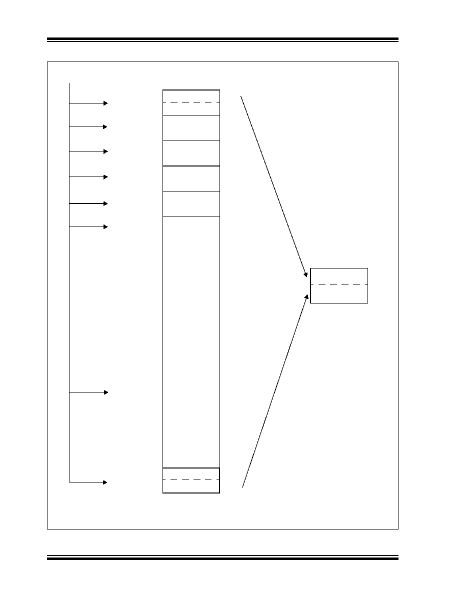
PIC18F2450/4450
DS39760A-page 60
Advance Information
� 2006 Microchip Technology Inc.
FIGURE 5-5:
DATA MEMORY MAP FOR PIC18F2450/4450 DEVICES
Bank 0
Bank 1
Bank 14
Bank 15
Data Memory Map
BSR<3:0>
= 0000
= 0001
= 1111
060h
05Fh
F60h
FFFh
00h
5Fh
60h
FFh
Access Bank
When a = 0:
The BSR is ignored and the
Access Bank is used.
The first 96 bytes are
general purpose RAM
(from Bank 0).
The remaining 160 bytes are
Special Function Registers
(from Bank 15).
When a = 1:
The BSR specifies the bank
used by the instruction.
F5Fh
F00h
EFFh
1FFh
100h
0FFh
000h
Access RAM
FFh
00h
FFh
00h
FFh
00h
GPR
GPR
SFR
Access RAM High
Access RAM Low
Bank 2
= 0010
(SFRs)
2FFh
200h
3FFh
300h
4FFh
400h
800h
Bank 3
Bank 4
Bank 5
FFh
00h
FFh
00h
FFh
00h
00h
Unused
Unused
FFh
= 0011
= 0100
= 0101
Unused
Read as 00h
to
= 1110
Note 1:
This bank also serve as RAM buffer for USB operation. See Section 5.3.1 "USB RAM" for more
information.
Unused
GPR
(1)
Read as 00h
Read as 00h
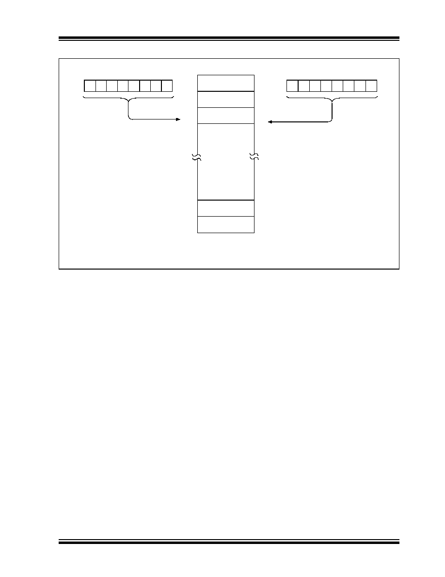
PIC18F2450/4450
� 2006 Microchip Technology Inc.
Advance Information
DS39760A-page 61
FIGURE 5-6:
USE OF THE BANK SELECT REGISTER (DIRECT ADDRESSING)
5.3.3
ACCESS BANK
While the use of the BSR, with an embedded 8-bit
address, allows users to address the entire range of
data memory, it also means that the user must always
ensure that the correct bank is selected. Otherwise,
data may be read from or written to the wrong location.
This can be disastrous if a GPR is the intended target
of an operation but an SFR is written to instead.
Verifying and/or changing the BSR for each read or
write to data memory can become very inefficient.
To streamline access for the most commonly used data
memory locations, the data memory is configured with
an Access Bank, which allows users to access a
mapped block of memory without specifying a BSR.
The Access Bank consists of the first 96 bytes of
memory (00h-5Fh) in Bank 0 and the last 160 bytes of
memory (60h-FFh) in Block 15. The lower half is known
as the "Access RAM" and is composed of GPRs. The
upper half is where the device's SFRs are mapped.
These two areas are mapped contiguously in the
Access Bank and can be addressed in a linear fashion
by an 8-bit address (Figure 5-5).
The Access Bank is used by core PIC18 instructions
that include the Access RAM bit (the `a' parameter in
the instruction). When `a' is equal to `1', the instruction
uses the BSR and the 8-bit address included in the
opcode for the data memory address. When `a' is `0',
however, the instruction is forced to use the Access
Bank address map; the current value of the BSR is
ignored entirely.
Using this "forced" addressing allows the instruction to
operate on a data address in a single cycle without
updating the BSR first. For 8-bit addresses of 60h and
above, this means that users can evaluate and operate
on SFRs more efficiently. The Access RAM below 60h
is a good place for data values that the user might need
to access rapidly, such as immediate computational
results or common program variables. Access RAM
also allows for faster and more code efficient context
saving and switching of variables.
The mapping of the Access Bank is slightly different
when the extended instruction set is enabled (XINST
Configuration bit = 1). This is discussed in more detail
in Section 5.6.3 "Mapping the Access Bank in
Indexed Literal Offset Mode".
5.3.4
GENERAL PURPOSE
REGISTER FILE
PIC18 devices may have banked memory in the GPR
area. This is data RAM which is available for use by all
instructions. GPRs start at the bottom of Bank 0
(address 000h) and grow upwards towards the bottom of
the SFR area. GPRs are not initialized by a Power-on
Reset and are unchanged on all other Resets.
Note
1:
The Access RAM bit of the instruction can be used to force an override of the selected bank (BSR<3:0>) to
the registers of the Access Bank.
2:
The MOVFF instruction embeds the entire 12-bit address in the instruction.
Data Memory
Bank Select
(2)
7
0
From Opcode
(2)
0
0
0
0
000h
100h
200h
300h
F00h
E00h
FFFh
Bank 0
Bank 1
Bank 2
Bank 14
Bank 15
00h
FFh
00h
FFh
00h
FFh
00h
FFh
00h
FFh
00h
FFh
Bank 3
through
Bank 13
0
0
1
1
1
1
1
1
1
1
1
1
7
0
BSR
(1)

PIC18F2450/4450
DS39760A-page 62
Advance Information
� 2006 Microchip Technology Inc.
5.3.5
SPECIAL FUNCTION REGISTERS
The Special Function Registers (SFRs) are registers
used by the CPU and peripheral modules for controlling
the desired operation of the device. These registers are
implemented as static RAM in the data memory space.
SFRs start at the top of data memory and extend
downward to occupy the top segment of Bank 15, from
F60h to FFFh. A list of these registers is given in
Table 5-1 and Table 5-2.
The SFRs can be classified into two sets: those
associated with the "core" device functionality (ALU,
Resets and interrupts) and those related to the
peripheral functions. The Reset and interrupt registers
are described in their respective chapters, while the
ALU's STATUS register is described later in this
section. Registers related to the operation of a
peripheral feature are described in the chapter for that
peripheral.
The SFRs are typically distributed among the
peripherals whose functions they control. Unused SFR
locations are unimplemented and read as `0's.
TABLE 5-1:
SPECIAL FUNCTION REGISTER MAP FOR PIC18F2450/4450 DEVICES
Address
Name
Address
Name
Address
Name
Address
Name
Address
Name
FFFh
TOSU
FDFh
INDF2
(1)
FBFh
CCPR1H
F9Fh
IPR1
F7Fh
UEP15
FFEh
TOSH
FDEh POSTINC2
(1)
FBEh
CCPR1L
F9Eh
PIR1
F7Eh
UEP14
FFDh
TOSL
FDDh POSTDEC2
(1)
FBDh
CCP1CON
F9Dh
PIE1
F7Dh
UEP13
FFCh
STKPTR
FDCh
PREINC2
(1)
FBCh
--
(2)
F9Ch
--
(2)
F7Ch
UEP12
FFBh
PCLATU
FDBh
PLUSW2
(1)
FBBh
--
(2)
F9Bh
--
(2)
F7Bh
UEP11
FFAh
PCLATH
FDAh
FSR2H
FBAh
--
(2)
F9Ah
--
(2)
F7Ah
UEP10
FF9h
PCL
FD9h
FSR2L
FB9h
--
(2)
F99h
--
(2)
F79h
UEP9
FF8h
TBLPTRU
FD8h
STATUS
FB8h
BAUDCON
F98h
--
(2)
F78h
UEP8
FF7h
TBLPTRH
FD7h
TMR0H
FB7h
--
(2)
F97h
--
(2)
F77h
UEP7
FF6h
TBLPTRL
FD6h
TMR0L
FB6h
--
(2)
F96h
TRISE
(3)
F76h
UEP6
FF5h
TABLAT
FD5h
T0CON
FB5h
--
(2)
F95h
TRISD
(3)
F75h
UEP5
FF4h
PRODH
FD4h
--
(2)
FB4h
--
(2)
F94h
TRISC
F74h
UEP4
FF3h
PRODL
FD3h
OSCCON
FB3h
--
(2)
F93h
TRISB
F73h
UEP3
FF2h
INTCON
FD2h
HLVDCON
FB2h
--
(2)
F92h
TRISA
F72h
UEP2
FF1h
INTCON2
FD1h
WDTCON
FB1h
--
(2)
F91h
--
(2)
F71h
UEP1
FF0h
INTCON3
FD0h
RCON
FB0h
SPBRGH
F90h
--
(2)
F70h
UEP0
FEFh
INDF0
(1)
FCFh
TMR1H
FAFh
SPBRG
F8Fh
--
(2)
F6Fh
UCFG
FEEh POSTINC0
(1)
FCEh
TMR1L
FAEh
RCREG
F8Eh
--
(2)
F6Eh
UADDR
FEDh POSTDEC0
(1)
FCDh
T1CON
FADh
TXREG
F8Dh
LATE
(3)
F6Dh
UCON
FECh
PREINC0
(1)
FCCh
TMR2
FACh
TXSTA
F8Ch
LATD
(3)
F6Ch
USTAT
FEBh
PLUSW0
(1)
FCBh
PR2
FABh
RCSTA
F8Bh
LATC
F6Bh
UEIE
FEAh
FSR0H
FCAh
T2CON
FAAh
--
(2)
F8Ah
LATB
F6Ah
UEIR
FE9h
FSR0L
FC9h
--
(2)
FA9h
--
(2)
F89h
LATA
F69h
UIE
FE8h
WREG
FC8h
--
(2)
FA8h
--
(2)
F88h
--
(2)
F68h
UIR
FE7h
INDF1
(1)
FC7h
--
(2)
FA7h
EECON2
(1)
F87h
--
(2)
F67h
UFRMH
FE6h POSTINC1
(1)
FC6h
--
(2)
FA6h
EECON1
F86h
--
(2)
F66h
UFRML
FE5h POSTDEC1
(1)
FC5h
--
(2)
FA5h
--
(2)
F85h
--
(2)
F65h
--
(2)
FE4h
PREINC1
(1)
FC4h
ADRESH
FA4h
--
(2)
F84h
PORTE
F64h
--
(2)
FE3h
PLUSW1
(1)
FC3h
ADRESL
FA3h
--
(2)
F83h
PORTD
(3)
F63h
--
(2)
FE2h
FSR1H
FC2h
ADCON0
FA2h
IPR2
F82h
PORTC
F62h
--
(2)
FE1h
FSR1L
FC1h
ADCON1
FA1h
PIR2
F81h
PORTB
F61h
--
(2)
FE0h
BSR
FC0h
ADCON2
FA0h
PIE2
F80h
PORTA
F60h
--
(2)
Note
1:
Not a physical register.
2:
Unimplemented registers are read as `0'.
3:
These registers are implemented only on 40/44-pin devices.
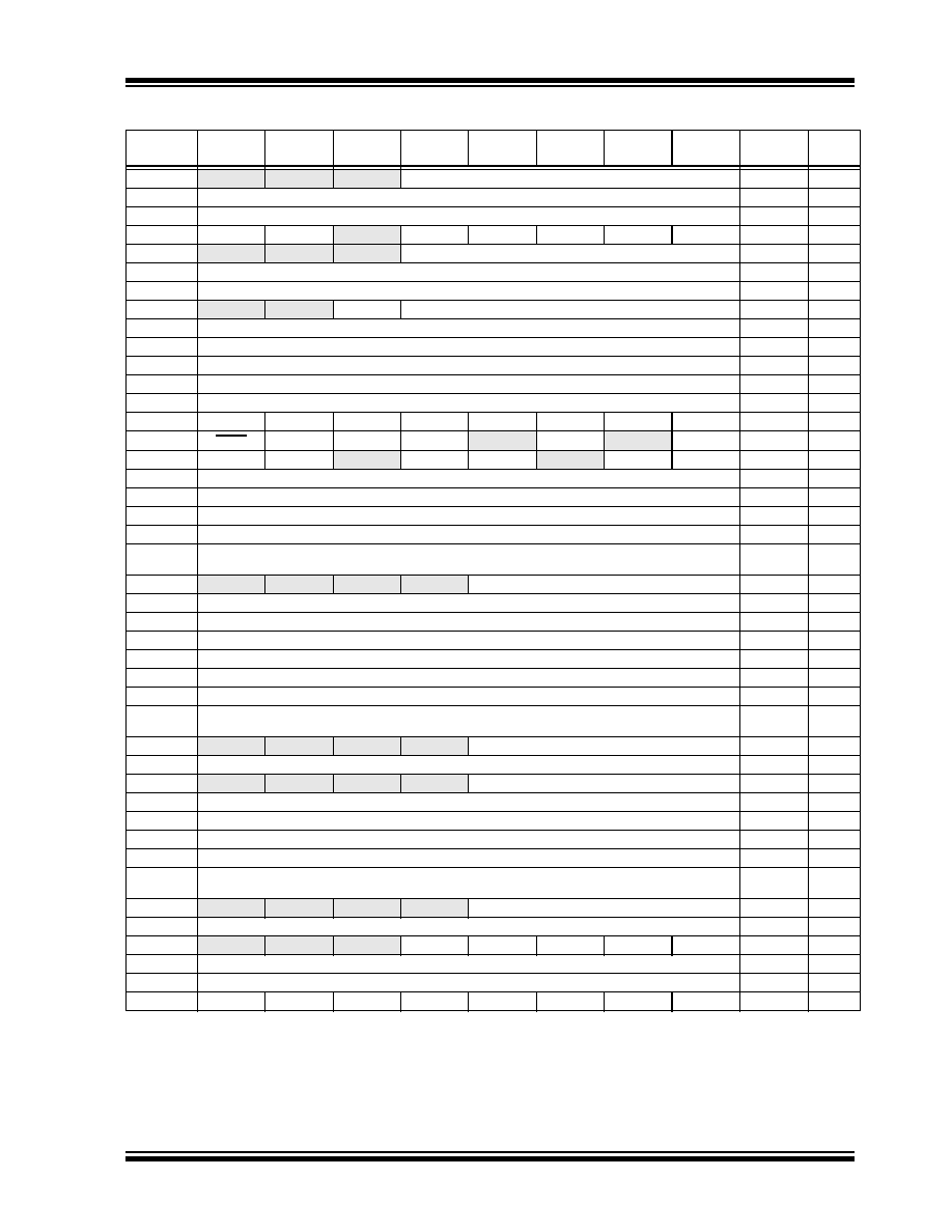
PIC18F2450/4450
� 2006 Microchip Technology Inc.
Advance Information
DS39760A-page 63
TABLE 5-2:
REGISTER FILE SUMMARY (PIC18F2450/4450)
File Name
Bit 7
Bit 6
Bit 5
Bit 4
Bit 3
Bit 2
Bit 1
Bit 0
Value on
POR, BOR
Details
on page
TOSU
--
--
--
Top-of-Stack Upper Byte (TOS<20:16>)
---0 0000
49, 54
TOSH
Top-of-Stack High Byte (TOS<15:8>)
0000 0000
49, 54
TOSL
Top-of-Stack Low Byte (TOS<7:0>)
0000 0000
49, 54
STKPTR
STKFUL
STKUNF
--
SP4
SP3
SP2
SP1
SP0
00-0 0000
49, 55
PCLATU
--
--
--
Holding Register for PC<20:16>
---0 0000
49, 54
PCLATH
Holding Register for PC<15:8>
0000 0000
49, 54
PCL
PC Low Byte (PC<7:0>)
0000 0000
49, 54
TBLPTRU
--
--
bit 21
(1)
Program Memory Table Pointer Upper Byte (TBLPTR<20:16>)
--00 0000
49, 76
TBLPTRH
Program Memory Table Pointer High Byte (TBLPTR<15:8>)
0000 0000
49, 76
TBLPTRL
Program Memory Table Pointer Low Byte (TBLPTR<7:0>)
0000 0000
49, 76
TABLAT
Program Memory Table Latch
0000 0000
49, 76
PRODH
Product Register High Byte
xxxx xxxx
49, 83
PRODL
Product Register Low Byte
xxxx xxxx
49, 83
INTCON
GIE/GIEH
PEIE/GIEL
TMR0IE
INT0IE
RBIE
TMR0IF
INT0IF
RBIF
0000 000x
49, 87
INTCON2
RBPU
INTEDG0
INTEDG1
INTEDG2
--
TMR0IP
--
RBIP
1111 -1-1
49, 88
INTCON3
INT2IP
INT1IP
--
INT2IE
INT1IE
--
INT2IF
INT1IF
11-0 0-00
49, 89
INDF0
Uses contents of FSR0 to address data memory � value of FSR0 not changed (not a physical register)
N/A
49, 68
POSTINC0
Uses contents of FSR0 to address data memory � value of FSR0 post-incremented (not a physical register)
N/A
49, 69
POSTDEC0
Uses contents of FSR0 to address data memory � value of FSR0 post-decremented (not a physical register)
N/A
49, 69
PREINC0
Uses contents of FSR0 to address data memory � value of FSR0 pre-incremented (not a physical register)
N/A
49, 69
PLUSW0
Uses contents of FSR0 to address data memory � value of FSR0 pre-incremented (not a physical register) �
value of FSR0 offset by W
N/A
49, 69
FSR0H
--
--
--
--
Indirect Data Memory Address Pointer 0 High Byte
---- 0000
49, 68
FSR0L
Indirect Data Memory Address Pointer 0 Low Byte
xxxx xxxx
49, 68
WREG
Working Register
xxxx xxxx
49,
INDF1
Uses contents of FSR1 to address data memory � value of FSR1 not changed (not a physical register)
N/A
49, 68
POSTINC1
Uses contents of FSR1 to address data memory � value of FSR1 post-incremented (not a physical register)
N/A
49, 69
POSTDEC1
Uses contents of FSR1 to address data memory � value of FSR1 post-decremented (not a physical register)
N/A
49, 69
PREINC1
Uses contents of FSR1 to address data memory � value of FSR1 pre-incremented (not a physical register)
N/A
49, 69
PLUSW1
Uses contents of FSR1 to address data memory � value of FSR1 pre-incremented (not a physical register) �
value of FSR1 offset by W
N/A
49, 69
FSR1H
--
--
--
--
Indirect Data Memory Address Pointer 1 High Byte
---- 0000
49, 68
FSR1L
Indirect Data Memory Address Pointer 1 Low Byte
xxxx xxxx
49, 68
BSR
--
--
--
--
Bank Select Register
---- 0000
49, 59
INDF2
Uses contents of FSR2 to address data memory � value of FSR2 not changed (not a physical register)
N/A
50, 68
POSTINC2
Uses contents of FSR2 to address data memory � value of FSR2 post-incremented (not a physical register)
N/A
50, 69
POSTDEC2
Uses contents of FSR2 to address data memory � value of FSR2 post-decremented (not a physical register)
N/A
50, 69
PREINC2
Uses contents of FSR2 to address data memory � value of FSR2 pre-incremented (not a physical register)
N/A
50, 69
PLUSW2
Uses contents of FSR2 to address data memory � value of FSR2 pre-incremented (not a physical register) �
value of FSR2 offset by W
N/A
50, 69
FSR2H
--
--
--
--
Indirect Data Memory Address Pointer 2 High Byte
---- 0000
50, 68
FSR2L
Indirect Data Memory Address Pointer 2 Low Byte
xxxx xxxx
50, 68
STATUS
--
--
--
N
OV
Z
DC
C
---x xxxx
50, 66
TMR0H
Timer0 Register High Byte
0000 0000
50, 113
TMR0L
Timer0 Register Low Byte
xxxx xxxx
50, 113
T0CON
TMR0ON
T08BIT
T0CS
T0SE
PSA
T0PS2
T0PS1
T0PS0
1111 1111
50, 111
Legend:
x
= unknown, u = unchanged, - = unimplemented, q = value depends on condition. Shaded cells are unimplemented, read as `0'.
Note
1:
Bit 21 of the TBLPTRU allows access to the device Configuration bits.
2:
The SBOREN bit is only available when BOREN<1:0> = 01; otherwise, the bit reads as `0'.
3:
These registers and/or bits are not implemented on 28-pin devices and are read as `0'. Reset values are shown for 40/44-pin devices;
individual unimplemented bits should be interpreted as `-'.
4:
RA6 is configured as a port pin based on various primary oscillator modes. When the port pin is disabled, all of the associated bits read `0'.
5:
RE3 is only available as a port pin when the MCLRE Configuration bit is clear; otherwise, the bit reads as `0'.
6:
RC5 and RC4 are only available as port pins when the USB module is disabled (UCON<3> = 0).
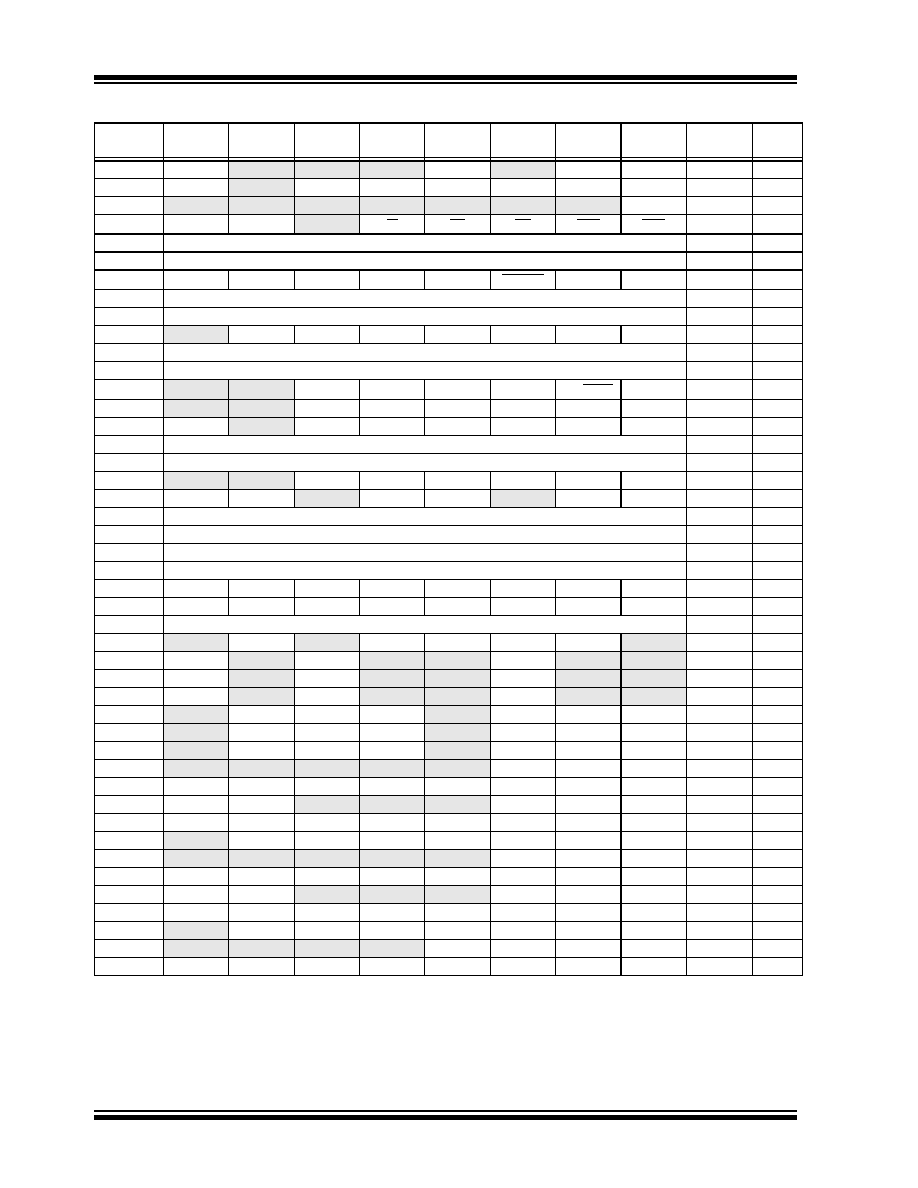
PIC18F2450/4450
DS39760A-page 64
Advance Information
� 2006 Microchip Technology Inc.
OSCCON
IDLEN
--
--
--
OSTS
--
SCS1
SCS0
0--- q-00
50, 31
HLVDCON
VDIRMAG
--
IRVST
HLVDEN
HLVDL3
HLVDL2
HLVDL1
HLVDL0
0-00 0101
50, 183
WDTCON
--
--
--
--
--
--
--
SWDTEN
--- ---0
50, 202
RCON
IPEN
SBOREN
(2)
--
RI
TO
PD
POR
BOR
0q-1 11q0
50, 42
TMR1H
Timer1 Register High Byte
xxxx xxxx
50, 119
TMR1L
Timer1 Register Low Byte
xxxx xxxx
50, 119
T1CON
RD16
T1RUN
T1CKPS1
T1CKPS0
T1OSCEN
T1SYNC
TMR1CS
TMR1ON
0000 0000
50, 115
TMR2
Timer2 Register
0000 0000
50, 122
PR2
Timer2 Period Register
1111 1111
50, 122
T2CON
--
T2OUTPS3
T2OUTPS2
T2OUTPS1
T2OUTPS0
TMR2ON
T2CKPS1
T2CKPS0
-000 0000
50, 121
ADRESH
A/D Result Register High Byte
xxxx xxxx
50, 182
ADRESL
A/D Result Register Low Byte
xxxx xxxx
50, 182
ADCON0
--
--
CHS3
CHS2
CHS1
CHS0
GO/DONE
ADON
--00 0000
50, 173
ADCON1
--
--
VCFG1
VCFG0
PCFG3
PCFG2
PCFG1
PCFG0
--00 qqqq
50, 174
ADCON2
ADFM
--
ACQT2
ACQT1
ACQT0
ADCS2
ADCS1
ADCS0
0-00 0000
50, 175
CCPR1H
Capture/Compare/PWM Register 1 High Byte
xxxx xxxx
50, 124
CCPR1L
Capture/Compare/PWM Register 1 Low Byte
xxxx xxxx
50, 124
CCP1CON
--
--
DC1B1
DC1B0
CCP1M3
CCP1M2
CCP1M1
CCP1M0
--00 0000
50, 123,
BAUDCON
ABDOVF
RCIDL
--
SCKP
BRG16
--
WUE
ABDEN
01-0 0-00
51, 156,
SPBRGH
EUSART Baud Rate Generator Register High Byte
0000 0000
50, 157
SPBRG
EUSART Baud Rate Generator Register Low Byte
0000 0000
50, 157
RCREG
EUSART Receive Register
0000 0000
50, 164
TXREG
EUSART Transmit Register
0000 0000
50, 162
TXSTA
CSRC
TX9
TXEN
SYNC
SENDB
BRGH
TRMT
TX9D
0000 0010
51, 154
RCSTA
SPEN
RX9
SREN
CREN
ADDEN
FERR
OERR
RX9D
0000 000x
51, 155
EECON2
Data Memory Control Register 2 (not a physical register)
0000 0000
51, 74
EECON1
--
CFGS
--
FREE
WRERR
WREN
WR
--
-x-0 x00-
51, 75
IPR2
OSCFIP
--
USBIP
--
--
HLVDIP
--
--
1-1- -1--
51, 95
PIR2
OSCFIF
--
USBIF
--
--
HLVDIF
--
--
0-0- -0--
51, 91
PIE2
OSCFIE
--
USBIE
--
--
HLVDIE
--
--
0-0- -0--
51, 93
IPR1
--
ADIP
RCIP
TXIP
--
CCP1IP
TMR2IP
TMR1IP
-111 -111
51, 94
PIR1
--
ADIF
RCIF
TXIF
--
CCP1IF
TMR2IF
TMR1IF
-000 -000
51, 90
PIE1
--
ADIE
RCIE
TXIE
--
CCP1IE
TMR2IE
TMR1IE
-000 -000
51, 92
TRISE
(3)
--
--
--
--
--
TRISE2
TRISE1
TRISE0
---- -111
51, 110
TRISD
(3)
TRISD7
TRISD6
TRISD5
TRISD4
TRISD3
TRISD2
TRISD1
TRISD0
1111 1111
51, 108
TRISC
TRISC7
TRISC6
--
--
--
TRISC2
TRISC1
TRISC0
11-- -111
51, 106
TRISB
TRISB7
TRISB6
TRISB5
TRISB4
TRISB3
TRISB2
TRISB1
TRISB0
1111 1111
51, 103
TRISA
--
TRISA6
(4)
TRISA5
TRISA4
TRISA3
TRISA2
TRISA1
TRISA0
-111 1111
51, 100
LATE
(3)
--
--
--
--
--
LATE2
LATE1
LATE0
---- -xxx
51, 110
LATD
(3)
LATD7
LATD6
LATD5
LATD4
LATD3
LATD2
LATD1
LATD0
xxxx xxxx
51, 108
LATC
LATC7
LATC6
--
--
--
LATC2
LATC1
LATC0
xx-- -xxx
51, 106
LATB
LATB7
LATB6
LATB5
LATB4
LATB3
LATB2
LATB1
LATB0
xxxx xxxx
51, 103
LATA
--
LATA6
(4)
LATA5
LATA4
LATA3
LATA2
LATA1
LATA0
-xxx xxxx
51, 100
PORTE
--
--
--
--
RE3
(5)
RE2
(3)
RE1
(3)
RE0
(3)
---- x000
51, 109
PORTD
(3)
RD7
RD6
RD5
RD4
RD3
RD2
RD1
RD0
xxxx xxxx
51, 108
TABLE 5-2:
REGISTER FILE SUMMARY (PIC18F2450/4450) (CONTINUED)
File Name
Bit 7
Bit 6
Bit 5
Bit 4
Bit 3
Bit 2
Bit 1
Bit 0
Value on
POR, BOR
Details
on page
Legend:
x
= unknown, u = unchanged, - = unimplemented, q = value depends on condition. Shaded cells are unimplemented, read as `0'.
Note
1:
Bit 21 of the TBLPTRU allows access to the device Configuration bits.
2:
The SBOREN bit is only available when BOREN<1:0> = 01; otherwise, the bit reads as `0'.
3:
These registers and/or bits are not implemented on 28-pin devices and are read as `0'. Reset values are shown for 40/44-pin devices;
individual unimplemented bits should be interpreted as `-'.
4:
RA6 is configured as a port pin based on various primary oscillator modes. When the port pin is disabled, all of the associated bits read `0'.
5:
RE3 is only available as a port pin when the MCLRE Configuration bit is clear; otherwise, the bit reads as `0'.
6:
RC5 and RC4 are only available as port pins when the USB module is disabled (UCON<3> = 0).
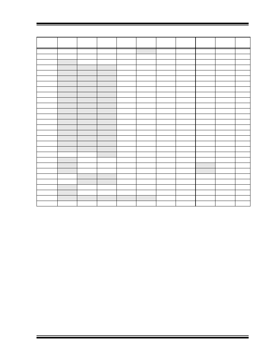
PIC18F2450/4450
� 2006 Microchip Technology Inc.
Advance Information
DS39760A-page 65
PORTC
RC7
RC6
RC5
(6)
RC4
(6)
--
RC2
RC1
RC0
xxxx -xxx
51, 106
PORTB
RB7
RB6
RB5
RB4
RB3
RB2
RB1
RB0
xxxx xxxx
51, 100
PORTA
--
RA6
(4)
RA5
RA4
RA3
RA2
RA1
RA0
-x0x 0000
51, 100
UEP15
--
--
--
EPHSHK
EPCONDIS
EPOUTEN
EPINEN
EPSTALL
---0 0000
51, 135
UEP14
--
--
--
EPHSHK
EPCONDIS
EPOUTEN
EPINEN
EPSTALL
---0 0000
51, 135
UEP13
--
--
--
EPHSHK
EPCONDIS
EPOUTEN
EPINEN
EPSTALL
---0 0000
51, 135
UEP12
--
--
--
EPHSHK
EPCONDIS
EPOUTEN
EPINEN
EPSTALL
---0 0000
51, 135
UEP11
--
--
--
EPHSHK
EPCONDIS
EPOUTEN
EPINEN
EPSTALL
---0 0000
51, 135
UEP10
--
--
--
EPHSHK
EPCONDIS
EPOUTEN
EPINEN
EPSTALL
---0 0000
51, 135
UEP9
--
--
--
EPHSHK
EPCONDIS
EPOUTEN
EPINEN
EPSTALL
---0 0000
51, 135
UEP8
--
--
--
EPHSHK
EPCONDIS
EPOUTEN
EPINEN
EPSTALL
---0 0000
52, 135
UEP7
--
--
--
EPHSHK
EPCONDIS
EPOUTEN
EPINEN
EPSTALL
---0 0000
52, 135
UEP6
--
--
--
EPHSHK
EPCONDIS
EPOUTEN
EPINEN
EPSTALL
---0 0000
52, 135
UEP5
--
--
--
EPHSHK
EPCONDIS
EPOUTEN
EPINEN
EPSTALL
---0 0000
52, 135
UEP4
--
--
--
EPHSHK
EPCONDIS
EPOUTEN
EPINEN
EPSTALL
---0 0000
52, 135
UEP3
--
--
--
EPHSHK
EPCONDIS
EPOUTEN
EPINEN
EPSTALL
---0 0000
52, 135
UEP2
--
--
--
EPHSHK
EPCONDIS
EPOUTEN
EPINEN
EPSTALL
---0 0000
52, 135
UEP1
--
--
--
EPHSHK
EPCONDIS
EPOUTEN
EPINEN
EPSTALL
---0 0000
52, 135
UEP0
--
--
--
EPHSHK
EPCONDIS
EPOUTEN
EPINEN
EPSTALL
---0 0000
52, 135
UCFG
UTEYE
UOEMON
--
UPUEN
UTRDIS
FSEN
PPB1
PPB0
00-0 0000
52, 132
UADDR
--
ADDR6
ADDR5
ADDR4
ADDR3
ADDR2
ADDR1
ADDR0
-000 0000
52, 136
UCON
--
PPBRST
SE0
PKTDIS
USBEN
RESUME
SUSPND
--
-0x0 000-
52, 130
USTAT
--
ENDP3
ENDP2
ENDP1
ENDP0
DIR
PPBI
--
-xxx xxx-
52, 134
UEIE
BTSEE
--
--
BTOEE
DFN8EE
CRC16EE
CRC5EE
PIDEE
0--0 0000
52, 147
UEIR
BTSEF
--
--
BTOEF
DFN8EF
CRC16EF
CRC5EF
PIDEF
0--0 0000
52, 146
UIE
--
SOFIE
STALLIE
IDLEIE
TRNIE
ACTVIE
UERRIE
URSTIE
-000 0000
52, 145
UIR
--
SOFIF
STALLIF
IDLEIF
TRNIF
ACTVIF
UERRIF
URSTIF
-000 0000
52, 144
UFRMH
--
--
--
--
--
FRM10
FRM9
FRM8
---- -xxx
52, 136
UFRML
FRM7
FRM6
FRM5
FRM4
FRM3
FRM2
FRM1
FRM0
xxxx xxxx
52, 136
TABLE 5-2:
REGISTER FILE SUMMARY (PIC18F2450/4450) (CONTINUED)
File Name
Bit 7
Bit 6
Bit 5
Bit 4
Bit 3
Bit 2
Bit 1
Bit 0
Value on
POR, BOR
Details
on page
Legend:
x
= unknown, u = unchanged, - = unimplemented, q = value depends on condition. Shaded cells are unimplemented, read as `0'.
Note
1:
Bit 21 of the TBLPTRU allows access to the device Configuration bits.
2:
The SBOREN bit is only available when BOREN<1:0> = 01; otherwise, the bit reads as `0'.
3:
These registers and/or bits are not implemented on 28-pin devices and are read as `0'. Reset values are shown for 40/44-pin devices;
individual unimplemented bits should be interpreted as `-'.
4:
RA6 is configured as a port pin based on various primary oscillator modes. When the port pin is disabled, all of the associated bits read `0'.
5:
RE3 is only available as a port pin when the MCLRE Configuration bit is clear; otherwise, the bit reads as `0'.
6:
RC5 and RC4 are only available as port pins when the USB module is disabled (UCON<3> = 0).
PIC18F2450/4450
DS39760A-page 66
Advance Information
� 2006 Microchip Technology Inc.
5.3.6
STATUS REGISTER
The STATUS register, shown in Register 5-2, contains
the arithmetic status of the ALU. As with any other SFR,
it can be the operand for any instruction.
If the STATUS register is the destination for an instruction
that affects the Z, DC, C, OV or N bits, the results of the
instruction are not written; instead, the STATUS register
is updated according to the instruction performed.
Therefore, the result of an instruction with the STATUS
register as its destination may be different than intended.
As an example, CLRF STATUS will set the Z bit and leave
the remaining Status bits unchanged (`000u u1uu').
It is recommended that only BCF, BSF, SWAPF, MOVFF
and MOVWF instructions are used to alter the STATUS
register because these instructions do not affect the Z,
C, DC, OV or N bits in the STATUS register.
For other instructions that do not affect Status bits, see
the instruction set summaries in Table 19-2 and
Table 19-3.
Note:
The C and DC bits operate as the Borrow
and Digit Borrow bits, respectively, in
subtraction.
REGISTER 5-2:
STATUS REGISTER
U-0
U-0
U-0
R/W-x
R/W-x
R/W-x
R/W-x
R/W-x
--
--
--
N
OV
Z
DC
(1)
C
(2)
bit 7
bit 0
Legend:
R = Readable bit
W = Writable bit
U = Unimplemented bit, read as `0'
-n = Value at POR
`1' = Bit is set
`0' = Bit is cleared
x = Bit is unknown
bit 7-5
Unimplemented: Read as `0'
bit 4
N: Negative bit
This bit is used for signed arithmetic (2's complement). It indicates whether the result was
negative (ALU MSB = 1).
1
= Result was negative
0
= Result was positive
bit 3
OV: Overflow bit
This bit is used for signed arithmetic (2's complement). It indicates an overflow of the 7-bit
magnitude which causes the sign bit (bit 7 of the result) to change state.
1
= Overflow occurred for signed arithmetic (in this arithmetic operation)
0
= No overflow occurred
bit 2
Z: Zero bit
1
= The result of an arithmetic or logic operation is zero
0
= The result of an arithmetic or logic operation is not zero
bit 1
DC: Digit Carry/Borrow bit
(1)
For ADDWF, ADDLW, SUBLW and SUBWF instructions:
1
= A carry-out from the 4th low-order bit of the result occurred
0
= No carry-out from the 4th low-order bit of the result
bit 0
C: Carry/Borrow bit
(2)
For ADDWF, ADDLW, SUBLW and SUBWF instructions:
1
= A carry-out from the Most Significant bit of the result occurred
0
= No carry-out from the Most Significant bit of the result occurred
Note 1:
For borrow, the polarity is reversed. A subtraction is executed by adding the 2's complement of the second
operand. For rotate (RRF, RLF) instructions, this bit is loaded with either bit 4 or bit 3 of the source register.
2:
For borrow, the polarity is reversed. A subtraction is executed by adding the 2's complement of the second
operand. For rotate (RRF, RLF) instructions, this bit is loaded with either the high or low-order bit of the
source register.

PIC18F2450/4450
� 2006 Microchip Technology Inc.
Advance Information
DS39760A-page 67
5.4
Data Addressing Modes
While the program memory can be addressed in only
one way � through the program counter � information
in the data memory space can be addressed in several
ways. For most instructions, the addressing mode is
fixed. Other instructions may use up to three modes,
depending on which operands are used and whether or
not the extended instruction set is enabled.
The addressing modes are:
� Inherent
� Literal
� Direct
� Indirect
An additional addressing mode, Indexed Literal Offset,
is available when the extended instruction set is
enabled (XINST Configuration bit = 1). Its operation is
discussed in greater detail in Section 5.6.1 "Indexed
Addressing with Literal Offset".
5.4.1
INHERENT AND LITERAL
ADDRESSING
Many PIC18 control instructions do not need any
argument at all; they either perform an operation that
globally affects the device or they operate implicitly on
one register. This addressing mode is known as
Inherent Addressing. Examples include SLEEP, RESET
and DAW.
Other instructions work in a similar way but require an
additional explicit argument in the opcode. This is
known as Literal Addressing mode because they
require some literal value as an argument. Examples
include ADDLW and MOVLW, which respectively, add or
move a literal value to the W register. Other examples
include CALL and GOTO, which include a 20-bit
program memory address.
5.4.2
DIRECT ADDRESSING
Direct Addressing mode specifies all or part of the
source and/or destination address of the operation
within the opcode itself. The options are specified by
the arguments accompanying the instruction.
In the core PIC18 instruction set, bit-oriented and byte-
oriented instructions use some version of Direct
Addressing by default. All of these instructions include
some 8-bit literal address as their Least Significant
Byte. This address specifies either a register address in
one of the banks of data RAM (Section 5.3.4 "General
Purpose Register File") or a location in the Access
Bank (Section 5.3.3 "Access Bank") as the data
source for the instruction.
The Access RAM bit `a' determines how the address is
interpreted. When `a' is `1', the contents of the BSR
(Section 5.3.2 "Bank Select Register (BSR)") are
used with the address to determine the complete 12-bit
address of the register. When `a' is `0', the address is
interpreted as being a register in the Access Bank.
Addressing that uses the Access RAM is sometimes
also known as Direct Forced Addressing mode.
A few instructions, such as MOVFF, include the entire
12-bit address (either source or destination) in their
opcodes. In these cases, the BSR is ignored entirely.
The destination of the operation's results is determined
by the destination bit `d'. When `d' is `1', the results are
stored back in the source register, overwriting its origi-
nal contents. When `d' is `0', the results are stored in
the W register. Instructions without the `d' argument
have a destination that is implicit in the instruction; their
destination is either the target register being operated
on or the W register.
5.4.3
INDIRECT ADDRESSING
Indirect Addressing allows the user to access a location
in data memory without giving a fixed address in the
instruction. This is done by using File Select Registers
(FSRs) as pointers to the locations to be read or written
to. Since the FSRs are themselves located in RAM as
Special Function Registers, they can also be directly
manipulated under program control. This makes FSRs
very useful in implementing data structures, such as
tables and arrays in data memory.
The registers for Indirect Addressing are also
implemented with Indirect File Operands (INDFs) that
permit automatic manipulation of the pointer value with
auto-incrementing, auto-decrementing or offsetting
with another value. This allows for efficient code, using
loops, such as the example of clearing an entire RAM
bank in Example 5-5.
EXAMPLE 5-5:
HOW TO CLEAR RAM
(BANK 1) USING
INDIRECT ADDRESSING
Note:
The execution of some instructions in the
core PIC18 instruction set are changed
when the PIC18 extended instruction
set is enabled. See Section 5.6 "Data
Memory and the Extended Instruction
Set" for more information.
LFSR
FSR0, 100h
;
NEXT
CLRF
POSTINC0
; Clear INDF
; register then
; inc pointer
BTFSS
FSR0H, 1
; All done with
; Bank1?
BRA
NEXT
; NO, clear next
CONTINUE
; YES, continue
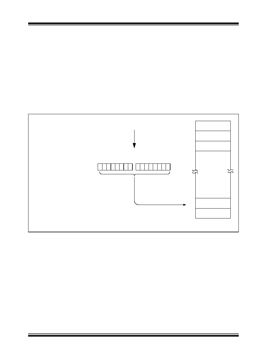
PIC18F2450/4450
DS39760A-page 68
Advance Information
� 2006 Microchip Technology Inc.
5.4.3.1
FSR Registers and the
INDF Operand
At the core of Indirect Addressing are three sets of
registers: FSR0, FSR1 and FSR2. Each represents a
pair of 8-bit registers: FSRnH and FSRnL. The four
upper bits of the FSRnH register are not used, so each
FSR pair holds a 12-bit value. This represents a value
that can address the entire range of the data memory
in a linear fashion. The FSR register pairs, then, serve
as pointers to data memory locations.
Indirect Addressing is accomplished with a set of
Indirect File Operands, INDF0 through INDF2. These
can be thought of as "virtual" registers; they are
mapped in the SFR space but are not physically
implemented. Reading or writing to a particular INDF
register actually accesses its corresponding FSR
register pair. A read from INDF1, for example, reads
the data at the address indicated by FSR1H:FSR1L.
Instructions that use the INDF registers as operands
actually use the contents of their corresponding FSR as
a pointer to the instruction's target. The INDF operand
is just a convenient way of using the pointer.
Because Indirect Addressing uses a full 12-bit address,
data RAM banking is not necessary. Thus, the current
contents of the BSR and the Access RAM bit have no
effect on determining the target address.
FIGURE 5-7:
INDIRECT ADDRESSING
FSR1H:FSR1L
0
7
Data Memory
000h
100h
200h
300h
F00h
E00h
FFFh
Bank 0
Bank 1
Bank 2
Bank 14
Bank 15
Bank 3
through
Bank 13
ADDWF, INDF1, 1
0
7
Using an instruction with one of the
indirect addressing registers as the
operand....
...uses the 12-bit address stored in
the FSR pair associated with that
register....
...to determine the data memory
location to be used in that operation.
In this case, the FSR1 pair contains
ECCh. This means the contents of
location ECCh will be added to that
of the W register and stored back in
ECCh.
x x x x 1 1 1 0
1 1 0 0 1 1 0 0
Bank 14

PIC18F2450/4450
� 2006 Microchip Technology Inc.
Advance Information
DS39760A-page 69
5.4.3.2
FSR Registers and POSTINC,
POSTDEC, PREINC and PLUSW
In addition to the INDF operand, each FSR register pair
also has four additional indirect operands. Like INDF,
these are "virtual" registers that cannot be indirectly
read or written to. Accessing these registers actually
accesses the associated FSR register pair, but also
performs a specific action on it stored value. They are:
� POSTDEC: accesses the FSR value, then
automatically decrements it by `1' afterwards
� POSTINC: accesses the FSR value, then
automatically increments it by `1' afterwards
� PREINC: increments the FSR value by `1', then
uses it in the operation
� PLUSW: adds the signed value of the W register
(range of -127 to 128) to that of the FSR and uses
the new value in the operation.
In this context, accessing an INDF register uses the
value in the FSR registers without changing them.
Similarly, accessing a PLUSW register gives the FSR
value offset by that in the W register; neither value is
actually changed in the operation. Accessing the other
virtual registers changes the value of the FSR
registers.
Operations on the FSRs with POSTDEC, POSTINC
and PREINC affect the entire register pair; that is,
rollovers of the FSRnL register from FFh to 00h carry
over to the FSRnH register. On the other hand, results
of these operations do not change the value of any
flags in the STATUS register (e.g., Z, N, OV, etc.).
The PLUSW register can be used to implement a form
of Indexed Addressing in the data memory space. By
manipulating the value in the W register, users can
reach addresses that are fixed offsets from pointer
addresses. In some applications, this can be used to
implement some powerful program control structure,
such as software stacks, inside of data memory.
5.4.3.3
Operations by FSRs on FSRs
Indirect Addressing operations that target other FSRs
or virtual registers represent special cases. For
example, using an FSR to point to one of the virtual
registers will not result in successful operations. As a
specific case, assume that FSR0H:FSR0L contains
FE7h, the address of INDF1. Attempts to read the
value of INDF1, using INDF0 as an operand, will return
00h. Attempts to write to INDF1, using INDF0 as the
operand, will result in a NOP.
On the other hand, using the virtual registers to write to
an FSR pair may not occur as planned. In these cases,
the value will be written to the FSR pair but without any
incrementing or decrementing. Thus, writing to INDF2
or POSTDEC2 will write the same value to the
FSR2H:FSR2L.
Since the FSRs are physical registers mapped in the
SFR space, they can be manipulated through all direct
operations. Users should proceed cautiously when
working on these registers, particularly if their code
uses Indirect Addressing.
Similarly, operations by Indirect Addressing are
generally permitted on all other SFRs. Users should
exercise the appropriate caution that they do not
inadvertently change settings that might affect the
operation of the device.

PIC18F2450/4450
DS39760A-page 70
Advance Information
� 2006 Microchip Technology Inc.
5.5
Program Memory and the
Extended Instruction Set
The operation of program memory is unaffected by the
use of the extended instruction set.
Enabling the extended instruction set adds eight
additional two-word commands to the existing
PIC18 instruction set: ADDFSR, ADDULNK, CALLW,
MOVSF
, MOVSS, PUSHL, SUBFSR and SUBULNK. These
instructions are executed as described in
Section 5.2.4 "Two-Word Instructions".
5.6
Data Memory and the Extended
Instruction Set
Enabling the PIC18 extended instruction set (XINST
Configuration bit = 1) significantly changes certain
aspects of data memory and its addressing.
Specifically, the use of the Access Bank for many of the
core PIC18 instructions is different. This is due to the
introduction of a new addressing mode for the data
memory space. This mode also alters the behavior of
Indirect Addressing using FSR2 and its associated
operands.
What does not change is just as important. The size of
the data memory space is unchanged, as well as its
linear addressing. The SFR map remains the same.
Core PIC18 instructions can still operate in both Direct
and Indirect Addressing mode; inherent and literal
instructions do not change at all. Indirect Addressing
with FSR0 and FSR1 also remains unchanged.
5.6.1
INDEXED ADDRESSING WITH
LITERAL OFFSET
Enabling the PIC18 extended instruction set changes
the behavior of Indirect Addressing using the FSR2
register pair and its associated file operands. Under the
proper conditions, instructions that use the Access
Bank � that is, most bit-oriented and byte-oriented
instructions � can invoke a form of Indexed Addressing
using an offset specified in the instruction. This special
addressing mode is known as Indexed Addressing with
Literal Offset or Indexed Literal Offset mode.
When using the extended instruction set, this
addressing mode requires the following:
� The use of the Access Bank is forced (`a' = 0);
and
� The file address argument is less than or equal
to 5Fh.
Under these conditions, the file address of the
instruction is not interpreted as the lower byte of an
address (used with the BSR in Direct Addressing), or
as an 8-bit address in the Access Bank. Instead, the
value is interpreted as an offset value to an Address
Pointer specified by FSR2. The offset and the contents
of FSR2 are added to obtain the target address of the
operation.
5.6.2
INSTRUCTIONS AFFECTED BY
INDEXED LITERAL OFFSET MODE
Any of the core PIC18 instructions that can use Direct
Addressing are potentially affected by the Indexed
Literal Offset Addressing mode. This includes all byte-
oriented and bit-oriented instructions, or almost one-half
of the standard PIC18 instruction set. Instructions that
only use Inherent or Literal Addressing modes are
unaffected.
Additionally, byte-oriented and bit-oriented instructions
are not affected if they use the Access Bank (Access
RAM bit is `1') or include a file address of 60h or above.
Instructions meeting these criteria will continue to
execute as before. A comparison of the different
possible addressing modes when the extended
instruction set is enabled in shown in Figure 5-8.
Those who desire to use byte-oriented or bit-oriented
instructions in the Indexed Literal Offset mode should
note the changes to assembler syntax for this mode.
This is described in more detail in Section 19.2.1
"Extended Instruction Syntax".
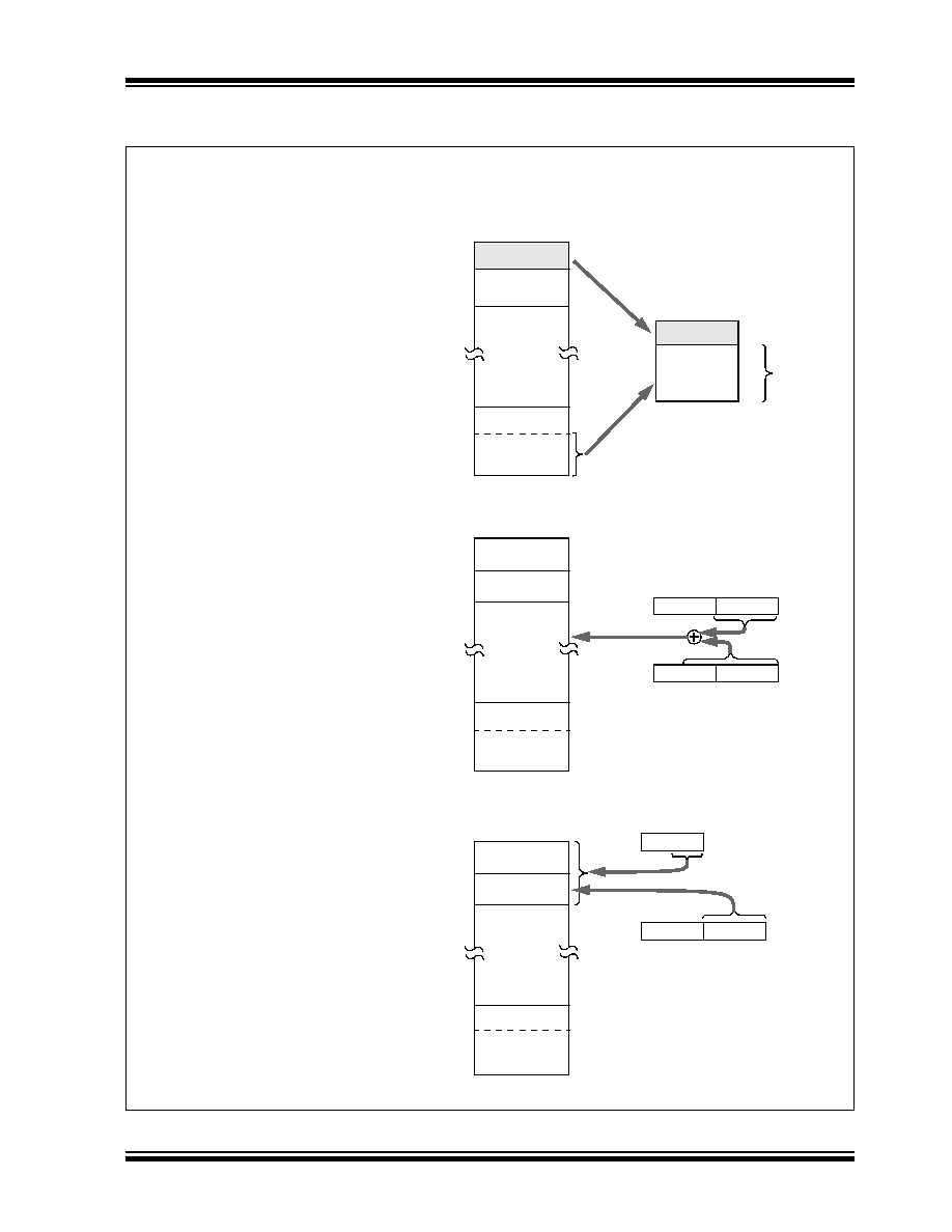
PIC18F2450/4450
� 2006 Microchip Technology Inc.
Advance Information
DS39760A-page 71
FIGURE 5-8:
COMPARING ADDRESSING OPTIONS FOR BIT-ORIENTED AND
BYTE-ORIENTED INSTRUCTIONS (EXTENDED INSTRUCTION SET ENABLED)
EXAMPLE INSTRUCTION: ADDWF, f, d, a (Opcode: 0010 01da ffff ffff)
When a = 0 and f
60h:
The instruction executes in
Direct Forced mode. `f' is inter-
preted as a location in the
Access RAM between 060h
and 0FFh. This is the same as
the SFRs or locations F60h to
0FFh (Bank 15) of data
memory.
Locations below 60h are not
available in this addressing
mode.
When a = 0 and f
5Fh:
The instruction executes in
Indexed Literal Offset mode. `f'
is interpreted as an offset to the
address value in FSR2. The
two are added together to
obtain the address of the target
register for the instruction. The
address can be anywhere in
the data memory space.
Note that in this mode, the
correct syntax is now:
ADDWF [k], d
where `k' is the same as `f'.
When a = 1 (all values of f):
The instruction executes in
Direct mode (also known as
Direct Long mode). `f' is inter-
preted as a location in one of
the 16 banks of the data
memory space. The bank is
designated by the Bank Select
Register (BSR). The address
can be in any implemented
bank in the data memory
space.
000h
060h
100h
F00h
F60h
FFFh
Valid range
00h
60h
FFh
Data Memory
Access RAM
Bank 0
Bank 1
through
Bank 14
Bank 15
SFRs
000h
080h
100h
F00h
F60h
FFFh
Data Memory
Bank 0
Bank 1
through
Bank 14
Bank 15
SFRs
FSR2H
FSR2L
ffffffff
001001da
ffffffff
001001da
000h
080h
100h
F00h
F60h
FFFh
Data Memory
Bank 0
Bank 1
through
Bank 14
Bank 15
SFRs
for `f'
BSR
00000000
080h
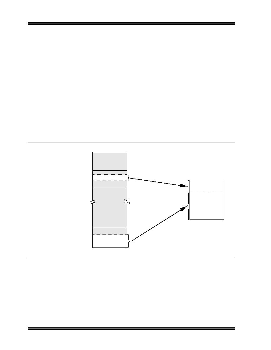
PIC18F2450/4450
DS39760A-page 72
Advance Information
� 2006 Microchip Technology Inc.
5.6.3
MAPPING THE ACCESS BANK IN
INDEXED LITERAL OFFSET MODE
The use of Indexed Literal Offset Addressing mode
effectively changes how the lower portion of Access
RAM (00h to 5Fh) is mapped. Rather than containing
just the contents of the bottom half of Bank 0, this mode
maps the contents from Bank 0 and a user-defined
"window" that can be located anywhere in the data
memory space. The value of FSR2 establishes the
lower boundary of the addresses mapped into the
window, while the upper boundary is defined by FSR2
plus 95 (5Fh). Addresses in the Access RAM above
5Fh are mapped as previously described (see
Section 5.3.3 "Access Bank"). An example of Access
Bank remapping in this addressing mode is shown in
Figure 5-9.
Remapping of the Access Bank applies
only to
operations using the Indexed Literal Offset mode.
Operations that use the BSR (Access RAM bit is `1') will
continue to use Direct Addressing as before. Any
indirect or indexed operation that explicitly uses any of
the indirect file operands (including FSR2) will continue
to operate as standard Indirect Addressing. Any
instruction that uses the Access Bank, but includes a
register address of greater than 05Fh, will use Direct
Addressing and the normal Access Bank map.
5.6.4
BSR IN INDEXED LITERAL
OFFSET MODE
Although the Access Bank is remapped when the
extended instruction set is enabled, the operation of the
BSR remains unchanged. Direct Addressing, using the
BSR to select the data memory bank, operates in the
same manner as previously described.
FIGURE 5-9:
REMAPPING THE ACCESS BANK WITH INDEXED LITERAL
OFFSET ADDRESSING
Data Memory
000h
100h
200h
F60h
F00h
FFFh
Bank 1
Bank 15
Bank 2
through
Bank 14
SFRs
ADDWF f, d, a
FSR2H:FSR2L = 120h
Locations in the region
from the FSR2 Pointer
(120h) to the pointer plus
05Fh (17Fh) are mapped
to the bottom of the
Access RAM (000h-05Fh).
Special Function Regis-
ters at F60h through FFFh
are mapped to 60h
through FFh as usual.
Bank 0 addresses below
5Fh are not available in
this mode. They can still
be addressed by using the
BSR.
Access Bank
00h
60h
FFh
Bank 0
SFRs
Bank 1 "Window"
Window
Example Situation:
120h
17Fh
5Fh
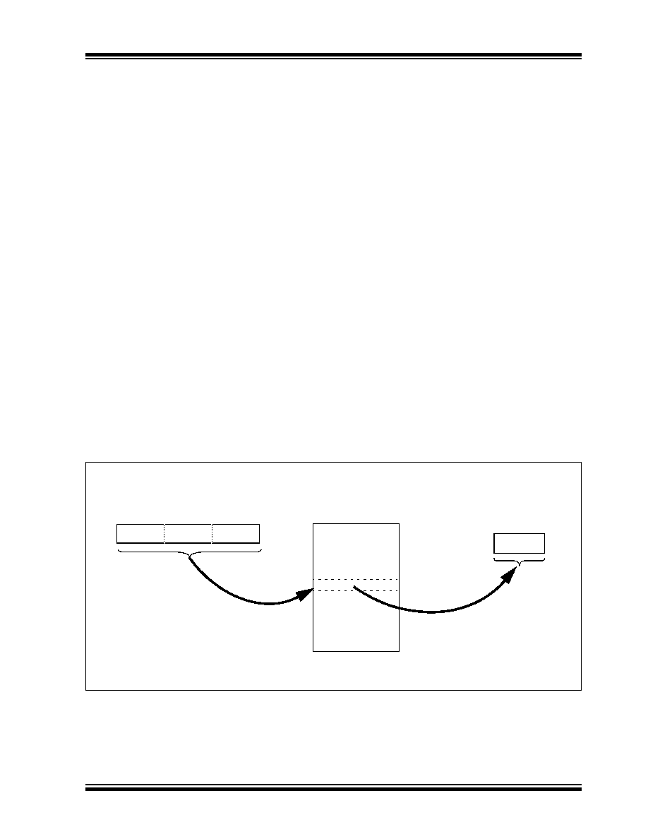
PIC18F2450/4450
� 2006 Microchip Technology Inc.
Advance Information
DS39760A-page 73
6.0
FLASH PROGRAM MEMORY
The Flash program memory is readable, writable and
erasable, during normal operation over the entire V
DD
range.
A read from program memory is executed on one byte
at a time. A write to program memory is executed on
blocks of 16 bytes at a time. Program memory is
erased in blocks of 64 bytes at a time. A Bulk Erase
operation may not be issued from user code.
Writing or erasing program memory will cease
instruction fetches until the operation is complete. The
program memory cannot be accessed during the write
or erase, therefore, code cannot execute. An internal
programming timer terminates program memory writes
and erases.
A value written to program memory does not need to be
a valid instruction. Executing a program memory
location that forms an invalid instruction results in a
NOP
.
6.1
Table Reads and Table Writes
In order to read and write program memory, there are
two operations that allow the processor to move bytes
between the program memory space and the data RAM:
� Table Read (TBLRD)
� Table Write (TBLWT)
The program memory space is 16 bits wide, while the
data RAM space is 8 bits wide. Table reads and table
writes move data between these two memory spaces
through an 8-bit register (TABLAT).
Table read operations retrieve data from program
memory and place it into the data RAM space.
Figure 6-1 shows the operation of a table read with
program memory and data RAM.
Table write operations store data from the data memory
space into holding registers in program memory. The
procedure to write the contents of the holding registers
into program memory is detailed in Section 6.5 "Writing
to Flash Program Memory". Figure 6-2 shows the
operation of a table write with program memory and data
RAM.
Table operations work with byte entities. A table block
containing data, rather than program instructions, is not
required to be word-aligned. Therefore, a table block can
start and end at any byte address. If a table write is being
used to write executable code into program memory,
program instructions will need to be word-aligned.
FIGURE 6-1:
TABLE READ OPERATION
Table Pointer
(1)
Table Latch (8-bit)
Program Memory
TBLPTRH
TBLPTRL
TABLAT
TBLPTRU
Instruction: TBLRD*
Note
1:
Table Pointer register points to a byte in program memory.
Program Memory
(TBLPTR)
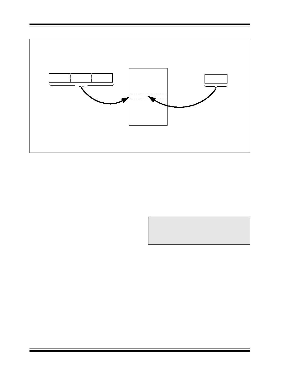
PIC18F2450/4450
DS39760A-page 74
Advance Information
� 2006 Microchip Technology Inc.
FIGURE 6-2:
TABLE WRITE OPERATION
6.2
Control Registers
Several control registers are used in conjunction with
the TBLRD and TBLWT instructions. These include the:
� EECON1 register
� EECON2 register
� TABLAT register
� TBLPTR registers
6.2.1
EECON1 AND EECON2 REGISTERS
The EECON1 register (Register 6-1) is the control
register for memory accesses. The EECON2 register is
not a physical register; it is used exclusively in the
memory write and erase sequences. Reading
EECON2 will read all `0's.
The CFGS control bit determines if the access will be
to the Configuration/Calibration registers or to program
memory.
The FREE bit, when set, will allow a program memory
erase operation. When FREE is set, the erase
operation is initiated on the next WR command. When
FREE is clear, only writes are enabled.
The WREN bit, when set, will allow a write operation.
On power-up, the WREN bit is clear. The WRERR bit is
set in hardware when the WREN bit is set and cleared
when the internal programming timer expires and the
write operation is complete.
The WR control bit initiates write operations. The bit
cannot be cleared, only set, in software; it is cleared in
hardware at the completion of the write operation.
Table Pointer
(1)
Table Latch (8-bit)
TBLPTRH
TBLPTRL
TABLAT
Program Memory
(TBLPTR)
TBLPTRU
Instruction: TBLWT*
Note
1:
Table Pointer actually points to one of 16 holding registers, the address of which is determined by
TBLPTRL<3:0>. The process for physically writing data to the program memory array is discussed
in Section 6.5 "Writing to Flash Program Memory".
Holding Registers
Program Memory
Note:
During normal operation, the WRERR is
read as `1'. This can indicate that a write
operation was prematurely terminated by
a Reset or a write operation was
attempted improperly.

PIC18F2450/4450
� 2006 Microchip Technology Inc.
Advance Information
DS39760A-page 75
REGISTER 6-1:
EECON1: MEMORY CONTROL REGISTER 1
U-0
R/W-x
U-0
R/W-0
R/W-x
R/W-0
R/S-0
U-0
--
CFGS
--
FREE
WRERR
(1)
WREN
WR
--
bit 7
bit 0
Legend:
R = Readable bit
W = Writable bit
U = Unimplemented bit, read as `0'
-n = Value at POR
`1' = Bit is set
`0' = Bit is cleared
x = Bit is unknown
bit 7
Unimplemented: Read as `0'
bit 6
CFGS: Flash Program or Configuration Select bit
1
= Access Configuration registers
0
= Access Flash program
bit 5
Unimplemented: Read as `0'
bit 4
FREE: Flash Row Erase Enable bit
1
= Erase the program memory row addressed by TBLPTR on the next WR command
(cleared by completion of erase operation)
0
= Perform write-only
bit 3
WRERR: Flash Program Error Flag bit
(1)
1
= A write operation is prematurely terminated (any Reset during self-timed programming in normal
operation or an improper write attempt)
0
= The write operation completed
bit 2
WREN: Flash Program Write Enable bit
1
= Allows write cycles to Flash program
0
= Inhibits write cycles to Flash program
bit 1
WR: Write Control bit
1
= Initiates a program memory erase cycle or write cycle
(The operation is self-timed and the bit is cleared by hardware once write is complete.
The WR bit can only be set (not cleared) in software.)
0
= Write cycle complete
bit 0
Unimplemented: Read as `0'
Note 1:
When a WRERR occurs, the CFGS bit is not cleared. This allows tracing of the error condition.
PIC18F2450/4450
DS39760A-page 76
Advance Information
� 2006 Microchip Technology Inc.
6.2.2
TABLE LATCH REGISTER (TABLAT)
The Table Latch (TABLAT) is an 8-bit register mapped
into the SFR space. The Table Latch register is used to
hold 8-bit data during data transfers between program
memory and data RAM.
6.2.3
TABLE POINTER REGISTER
(TBLPTR)
The Table Pointer (TBLPTR) register addresses a byte
within the program memory. The TBLPTR is comprised
of three SFR registers: Table Pointer Upper Byte, Table
Pointer High Byte and Table Pointer Low Byte
(TBLPTRU:TBLPTRH:TBLPTRL). These three registers
join to form a 22-bit wide pointer. The low-order 21 bits
allow the device to address up to 2 Mbytes of program
memory space. The 22nd bit allows access to the device
ID, the user ID and the Configuration bits.
The Table Pointer, TBLPTR, is used by the TBLRD and
TBLWT
instructions. These instructions can update the
TBLPTR in one of four ways based on the table opera-
tion. These operations are shown in Table 6-1. These
operations on the TBLPTR only affect the low-order
21 bits.
6.2.4
TABLE POINTER BOUNDARIES
TBLPTR is used in reads, writes and erases of the
Flash program memory.
When a TBLRD is executed, all 22 bits of the TBLPTR
determine which byte is read from program memory
into TABLAT.
When a TBLWT is executed, the four LSbs of the Table
Pointer register (TBLPTR<3:0>) determine which of the
16 program memory holding registers is written to.
When the timed write to program memory begins (via
the WR bit), the 16 MSbs of the TBLPTR
(TBLPTR<21:4>) determine which program memory
block of 16 bytes is written to. For more detail, see
Section 6.5 "Writing to Flash Program Memory".
When an erase of program memory is executed, the
16 MSbs of the Table Pointer register (TBLPTR<21:6>)
point to the 64-byte block that will be erased. The Least
Significant bits (TBLPTR<5:0>) are ignored.
Figure 6-3 describes the relevant boundaries of the
TBLPTR based on Flash program memory operations.
TABLE 6-1:
TABLE POINTER OPERATIONS WITH TBLRD AND TBLWT INSTRUCTIONS
FIGURE 6-3:
TABLE POINTER BOUNDARIES BASED ON OPERATION
Example
Operation on Table Pointer
TBLRD*
TBLWT*
TBLPTR is not modified
TBLRD*+
TBLWT*+
TBLPTR is incremented after the read/write
TBLRD*-
TBLWT*-
TBLPTR is decremented after the read/write
TBLRD+*
TBLWT+*
TBLPTR is incremented before the read/write
21
16
15
8
7
0
TABLE ERASE
TABLE READ � TBLPTR<21:0>
TBLPTRL
TBLPTRH
TBLPTRU
TBLPTR<21:6>
TABLE WRITE � TBLPTR<21:4>
PIC18F2450/4450
� 2006 Microchip Technology Inc.
Advance Information
DS39760A-page 77
6.3
Reading the Flash Program
Memory
The TBLRD instruction is used to retrieve data from
program memory and places it into data RAM. Table
reads from program memory are performed one byte at
a time.
TBLPTR points to a byte address in program space.
Executing TBLRD places the byte pointed to into
TABLAT. In addition, TBLPTR can be modified
automatically for the next table read operation.
The internal program memory is typically organized by
words. The Least Significant bit of the address selects
between the high and low bytes of the word. Figure 6-4
shows the interface between the internal program
memory and the TABLAT.
FIGURE 6-4:
READS FROM FLASH PROGRAM MEMORY
EXAMPLE 6-1:
READING A FLASH PROGRAM MEMORY WORD
(Even Byte Address)
Program Memory
(Odd Byte Address)
TBLRD
TABLAT
TBLPTR = xxxxx1
FETCH
Instruction Register
(IR)
Read Register
TBLPTR = xxxxx0
MOVLW
CODE_ADDR_UPPER
; Load TBLPTR with the base
MOVWF
TBLPTRU
; address of the word
MOVLW
CODE_ADDR_HIGH
MOVWF
TBLPTRH
MOVLW
CODE_ADDR_LOW
MOVWF
TBLPTRL
READ_WORD
TBLRD*+
; read into TABLAT and increment
MOVF
TABLAT, W
; get data
MOVWF
WORD_EVEN
TBLRD*+
; read into TABLAT and increment
MOVF
TABLAT, W
; get data
MOVF
WORD_ODD

PIC18F2450/4450
DS39760A-page 78
Advance Information
� 2006 Microchip Technology Inc.
6.4
Erasing Flash Program Memory
The minimum erase block is 32 words or 64 bytes. Only
through the use of an external programmer, or through
ICSP control, can larger blocks of program memory be
Bulk Erased. Word Erase in the Flash array is not
supported.
When initiating an erase sequence from the
microcontroller itself, a block of 64 bytes of program
memory is erased. The Most Significant 16 bits of the
TBLPTR<21:6> point to the block being erased.
TBLPTR<5:0> are ignored.
The EECON1 register commands the erase operation.
The WREN bit must be set to enable write operations.
The FREE bit is set to select an erase operation.
For protection, the write initiate sequence for EECON2
must be used.
A long write is necessary for erasing the internal Flash.
Instruction execution is halted while in a long write
cycle. The long write will be terminated by the internal
programming timer.
6.4.1
FLASH PROGRAM MEMORY
ERASE SEQUENCE
The sequence of events for erasing a block of internal
program memory is:
1.
Load Table Pointer register with address of row
being erased.
2.
Set the EECON1 register for the erase operation:
� clear the CFGS bit to access program memory;
� set WREN bit to enable writes;
� set FREE bit to enable the erase.
3.
Disable interrupts.
4.
Write 55h to EECON2.
5.
Write 0AAh to EECON2.
6.
Set the WR bit. This will begin the Row Erase
cycle.
7.
The CPU will stall for duration of the erase
(about 2 ms using internal timer).
8.
Re-enable interrupts.
EXAMPLE 6-2:
ERASING A FLASH PROGRAM MEMORY ROW
MOVLW
CODE_ADDR_UPPER
; load TBLPTR with the base
MOVWF
TBLPTRU
; address of the memory block
MOVLW
CODE_ADDR_HIGH
MOVWF
TBLPTRH
MOVLW
CODE_ADDR_LOW
MOVWF
TBLPTRL
ERASE_ROW
BCF
EECON1, CFGS
; access Flash program memory
BSF
EECON1, WREN
; enable write to memory
BSF
EECON1, FREE
; enable Row Erase operation
BCF
INTCON, GIE
; disable interrupts
Required
MOVLW
55h
Sequence
MOVWF
EECON2
; write 55h
MOVLW
0AAh
MOVWF
EECON2
; write 0AAh
BSF
EECON1, WR
; start erase (CPU stall)
BSF
INTCON, GIE
; re-enable interrupts
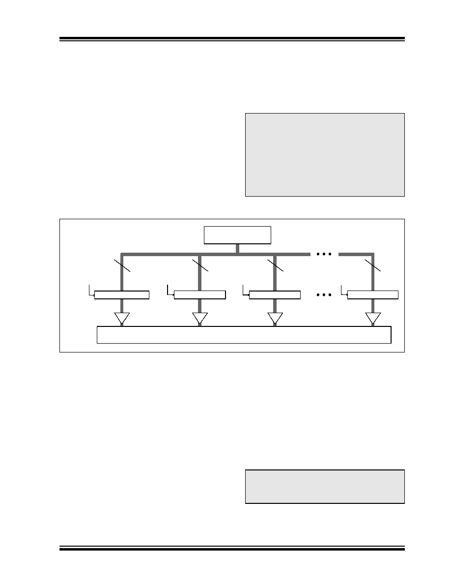
PIC18F2450/4450
� 2006 Microchip Technology Inc.
Advance Information
DS39760A-page 79
6.5
Writing to Flash Program Memory
The minimum programming block is 8 words or
16 bytes. Word or byte programming is not supported.
Table writes are used internally to load the holding
registers needed to program the Flash memory. There
are 16 holding registers used by the table writes for
programming.
Since the Table Latch (TABLAT) is only a single byte, the
TBLWT
instruction may need to be executed 16 times for
each programming operation. All of the table write oper-
ations will essentially be short writes because only the
holding registers are written. At the end of updating the
16 holding registers, the EECON1 register must be
written to in order to start the programming operation
with a long write.
The long write is necessary for programming the
internal Flash. Instruction execution is halted while in a
long write cycle. The long write will be terminated by
the internal programming timer.
The write/erase voltages are generated by an on-chip
charge pump, rated to operate over the voltage range
of the device.
FIGURE 6-5:
TABLE WRITES TO FLASH PROGRAM MEMORY
6.5.1
FLASH PROGRAM MEMORY WRITE
SEQUENCE
The sequence of events for programming an internal
program memory location should be:
1.
Read 64 bytes into RAM.
2.
Update data values in RAM as necessary.
3.
Load Table Pointer register with address being
erased.
4.
Execute the Row Erase procedure.
5.
Load Table Pointer register with address of first
byte being written.
6.
Write 16 bytes into the holding registers with
auto-increment.
7.
Set the EECON1 register for the write operation:
� clear the CFGS bit to access program memory;
� set WREN to enable byte writes.
8.
Disable interrupts.
9.
Write 55h to EECON2.
10. Write 0AAh to EECON2.
11. Set the WR bit. This will begin the write cycle.
12. The CPU will stall for duration of the write (about
2 ms using internal timer).
13. Re-enable interrupts.
14. Repeat steps 6 through 14 once more to write
64 bytes.
15. Verify the memory (table read).
This procedure will require about 8 ms to update one
row of 64 bytes of memory. An example of the required
code is given in Example 6-3.
Note:
The default value of the holding registers on
device Resets and after write operations is
FFh. A write of FFh to a holding register
does not modify that byte. This means that
individual bytes of program memory may be
modified, provided that the change does not
attempt to change any bit from a `0' to a `1'.
When modifying individual bytes, it is not
necessary to load all 16 holding registers
before executing a write operation.
TBLPTR = xxxxxF
TBLPTR = xxxxx1
TBLPTR = xxxxx0
TBLPTR = xxxxx2
Program Memory
Holding Register
Holding Register
Holding Register
Holding Register
8
8
8
8
TABLAT
Write Register
Note:
Before setting the WR bit, the Table
Pointer address needs to be within the
intended address range of the 16 bytes in
the holding register.

PIC18F2450/4450
DS39760A-page 80
Advance Information
� 2006 Microchip Technology Inc.
EXAMPLE 6-3:
WRITING TO FLASH PROGRAM MEMORY
MOVLW
D'64'
; number of bytes in erase block
MOVWF
COUNTER
MOVLW
BUFFER_ADDR_HIGH
; point to buffer
MOVWF
FSR0H
MOVLW
BUFFER_ADDR_LOW
MOVWF
FSR0L
MOVLW
CODE_ADDR_UPPER
; Load TBLPTR with the base
MOVWF
TBLPTRU
; address of the memory block
MOVLW
CODE_ADDR_HIGH
MOVWF
TBLPTRH
MOVLW
CODE_ADDR_LOW
MOVWF
TBLPTRL
READ_BLOCK
TBLRD*+
; read into TABLAT, and inc
MOVF
TABLAT, W
; get data
MOVWF
POSTINC0
; store data
DECFSZ
COUNTER ;
done?
BRA
READ_BLOCK
; repeat
MODIFY_WORD
MOVLW
DATA_ADDR_HIGH
; point to buffer
MOVWF
FSR0H
MOVLW
DATA_ADDR_LOW
MOVWF
FSR0L
MOVLW
NEW_DATA_LOW
; update buffer word
MOVWF
POSTINC0
MOVLW
NEW_DATA_HIGH
MOVWF
INDF0
ERASE_BLOCK
MOVLW
CODE_ADDR_UPPER
; load TBLPTR with the base
MOVWF
TBLPTRU
; address of the memory block
MOVLW
CODE_ADDR_HIGH
MOVWF
TBLPTRH
MOVLW
CODE_ADDR_LOW
MOVWF
TBLPTRL
BCF
EECON1, CFGS
; access Flash program memory
BSF
EECON1, WREN
; enable write to memory
BSF
EECON1, FREE
; enable Row Erase operation
BCF
INTCON, GIE
; disable interrupts
MOVLW
55h
Required
MOVWF
EECON2
; write 55h
Sequence
MOVLW
0AAh
MOVWF
EECON2
; write 0AAh
BSF
EECON1, WR
; start erase (CPU stall)
BSF
INTCON, GIE
; re-enable interrupts
TBLRD*-
; dummy read decrement
MOVLW
BUFFER_ADDR_HIGH
; point to buffer
MOVWF
FSR0H
MOVLW
BUFFER_ADDR_LOW
MOVWF
FSR0L
MOVLW
D'4'
MOVWF
COUNTER1
WRITE_BUFFER_BACK
MOVLW
D'16'
; number of bytes in holding register
MOVWF
COUNTER
WRITE_BYTE_TO_HREGS
MOVF
POSTINC0, W
; get low byte of buffer data
MOVWF
TABLAT
; present data to table latch
TBLWT+*
; write data, perform a short write
; to internal TBLWT holding register.
DECFSZ
COUNTER
; loop until buffers are full
BRA
WRITE_WORD_TO_HREGS
PIC18F2450/4450
� 2006 Microchip Technology Inc.
Advance Information
DS39760A-page 81
EXAMPLE 6-3:
WRITING TO FLASH PROGRAM MEMORY (CONTINUED)
6.5.2
WRITE VERIFY
Depending on the application, good programming
practice may dictate that the value written to the
memory should be verified against the original value.
This should be used in applications where excessive
writes can stress bits near the specification limit.
6.5.3
UNEXPECTED TERMINATION OF
WRITE OPERATION
If a write is terminated by an unplanned event, such as
loss of power or an unexpected Reset, the memory
location just programmed should be verified and
reprogrammed if needed. If the write operation is
interrupted by a MCLR Reset or a WDT Time-out Reset
during normal operation, the user can check the
WRERR bit and rewrite the location(s) as needed.
6.5.4
PROTECTION AGAINST SPURIOUS
WRITES
To protect against spurious writes to Flash program
memory, the write initiate sequence must also be
followed. See Section 18.0 "Special Features of the
CPU" for more detail.
6.6
Flash Program Operation During
Code Protection
See Section 18.5 "Program Verification and Code
Protection" for details on code protection of Flash
program memory.
TABLE 6-2:
REGISTERS ASSOCIATED WITH PROGRAM FLASH MEMORY
PROGRAM_MEMORY
BCF
EECON1, CFGS
; access Flash program memory
BSF
EECON1, WREN
; enable write to memory
BCF
INTCON, GIE
; disable interrupts
MOVLW
55h
Required
MOVWF
EECON2
; write 55h
Sequence
MOVLW
0AAh
MOVWF
EECON2
; write 0AAh
BSF
EECON1, WR
; start program (CPU stall)
DECFSZ
COUNTER1
BRA
WRITE_BUFFER_BACK
BSF
INTCON, GIE
; re-enable interrupts
BCF
EECON1, WREN
; disable write to memory
Name
Bit 7
Bit 6
Bit 5
Bit 4
Bit 3
Bit 2
Bit 1
Bit 0
Reset
Values
on page
TBLPTRU
--
--
bit 21
Program Memory Table Pointer Upper Byte (TBLPTR<20:16>)
49
TBPLTRH
Program Memory Table Pointer High Byte (TBLPTR<15:8>)
49
TBLPTRL
Program Memory Table Pointer Low Byte (TBLPTR<7:0>)
49
TABLAT
Program Memory Table Latch
49
INTCON
GIE/GIEH PEIE/GIEL TMR0IE
INT0IE
RBIE
TMR0IF
INT0IF
RBIF
49
EECON2
Control Register 2 (not a physical register)
51
EECON1
--
CFGS
--
FREE
WRERR
WREN
WR
--
51
IPR2
OSCFIP
--
USBIP
--
--
HLVDIP
--
--
51
PIR2
OSCFIF
--
USBIF
--
--
HLVDIF
--
--
51
PIE2
OSCFIE
--
USBIE
--
--
HLVDIE
--
--
51
Legend: -- = unimplemented, read as `0'. Shaded cells are not used during Flash access.

PIC18F2450/4450
DS39760A-page 82
Advance Information
� 2006 Microchip Technology Inc.
NOTES:
PIC18F2450/4450
� 2006 Microchip Technology Inc.
Advance Information
DS39760A-page 83
7.0
8 x 8 HARDWARE MULTIPLIER
7.1
Introduction
All PIC18 devices include an 8 x 8 hardware multiplier
as part of the ALU. The multiplier performs an unsigned
operation and yields a 16-bit result that is stored in the
product register pair, PRODH:PRODL. The multiplier's
operation does not affect any flags in the STATUS
register.
Making multiplication a hardware operation allows it to
be completed in a single instruction cycle. This has the
advantages of higher computational throughput and
reduced code size for multiplication algorithms and
allows the PIC18 devices to be used in many applica-
tions previously reserved for digital signal processors.
A comparison of various hardware and software
multiply operations, along with the savings in memory
and execution time, is shown in Table 7-1.
7.2
Operation
Example 7-1 shows the instruction sequence for an
8 x 8 unsigned multiplication. Only one instruction is
required when one of the arguments is already loaded
in the WREG register.
Example 7-2 shows the sequence to do an 8 x 8 signed
multiplication. To account for the sign bits of the
arguments, each argument's Most Significant bit (MSb)
is tested and the appropriate subtractions are done.
EXAMPLE 7-1:
8 x 8 UNSIGNED
MULTIPLY ROUTINE
EXAMPLE 7-2:
8 x 8 SIGNED MULTIPLY
ROUTINE
TABLE 7-1:
PERFORMANCE COMPARISON FOR VARIOUS MULTIPLY OPERATIONS
MOVF
ARG1, W
;
MULWF
ARG2
; ARG1 * ARG2 ->
; PRODH:PRODL
MOVF
ARG1, W
MULWF
ARG2
; ARG1 * ARG2 ->
; PRODH:PRODL
BTFSC
ARG2, SB
; Test Sign Bit
SUBWF
PRODH, F
; PRODH = PRODH
; - ARG1
MOVF
ARG2, W
BTFSC
ARG1, SB
; Test Sign Bit
SUBWF
PRODH, F
; PRODH = PRODH
; - ARG2
Routine
Multiply Method
Program
Memory
(Words)
Cycles
(Max)
Time
@ 40 MHz
@ 10 MHz
@ 4 MHz
8 x 8 unsigned
Without hardware multiply
13
69
6.9
s
27.6
s
69
s
Hardware multiply
1
1
100 ns
400 ns
1
s
8 x 8 signed
Without hardware multiply
33
91
9.1
s
36.4
s
91
s
Hardware multiply
6
6
600 ns
2.4
s
6
s
16 x 16 unsigned
Without hardware multiply
21
242
24.2
s
96.8
s
242
s
Hardware multiply
28
28
2.8
s
11.2
s
28
s
16 x 16 signed
Without hardware multiply
52
254
25.4
s
102.6
s
254
s
Hardware multiply
35
40
4.0
s
16.0
s
40
s

PIC18F2450/4450
DS39760A-page 84
Advance Information
� 2006 Microchip Technology Inc.
Example 7-3 shows the sequence to do a 16 x 16
unsigned multiplication. Equation 7-1 shows the
algorithm that is used. The 32-bit result is stored in four
registers (RES3:RES0).
EQUATION 7-1:
16 x 16 UNSIGNED
MULTIPLICATION
ALGORITHM
EXAMPLE 7-3:
16 x 16 UNSIGNED
MULTIPLY ROUTINE
Example 7-4 shows the sequence to do a 16 x 16
signed multiply. Equation 7-2 shows the algorithm
used. The 32-bit result is stored in four registers
(RES3:RES0). To account for the sign bits of the
arguments, the MSb for each argument pair is tested
and the appropriate subtractions are done.
EQUATION 7-2:
16 x 16 SIGNED
MULTIPLICATION
ALGORITHM
EXAMPLE 7-4:
16 x 16 SIGNED
MULTIPLY ROUTINE
RES3:RES0
=
ARG1H:ARG1L
� ARG2H:ARG2L
=
(ARG1H
� ARG2H � 2
16
) +
(ARG1H
� ARG2L � 2
8
) +
(ARG1L
� ARG2H � 2
8
) +
(ARG1L
� ARG2L)
MOVF
ARG1L, W
MULWF
ARG2L
; ARG1L * ARG2L->
; PRODH:PRODL
MOVFF
PRODH, RES1
;
MOVFF
PRODL, RES0
;
;
MOVF
ARG1H, W
MULWF
ARG2H
; ARG1H * ARG2H->
; PRODH:PRODL
MOVFF
PRODH, RES3
;
MOVFF
PRODL, RES2
;
;
MOVF
ARG1L, W
MULWF
ARG2H
; ARG1L * ARG2H->
; PRODH:PRODL
MOVF
PRODL, W
;
ADDWF
RES1, F
; Add cross
MOVF
PRODH, W
; products
ADDWFC
RES2, F
;
CLRF
WREG
;
ADDWFC
RES3, F
;
;
MOVF
ARG1H, W
;
MULWF
ARG2L
; ARG1H * ARG2L->
; PRODH:PRODL
MOVF
PRODL, W
;
ADDWF
RES1, F
; Add cross
MOVF
PRODH, W
; products
ADDWFC
RES2, F
;
CLRF
WREG
;
ADDWFC
RES3, F
;
RES3:RES0= ARG1H:ARG1L
� ARG2H:ARG2L
= (ARG1H
� ARG2H � 2
16
) +
(ARG1H
� ARG2L � 2
8
) +
(ARG1L
� ARG2H � 2
8
) +
(ARG1L
� ARG2L) +
(-1
� ARG2H<7> � ARG1H:ARG1L � 2
16
) +
(-1
� ARG1H<7> � ARG2H:ARG2L � 2
16
)
MOVF
ARG1L, W
MULWF
ARG2L
; ARG1L * ARG2L ->
; PRODH:PRODL
MOVFF
PRODH, RES1
;
MOVFF
PRODL, RES0
;
;
MOVF
ARG1H, W
MULWF
ARG2H
; ARG1H * ARG2H ->
; PRODH:PRODL
MOVFF
PRODH, RES3
;
MOVFF
PRODL, RES2
;
;
MOVF
ARG1L,W
MULWF
ARG2H
; ARG1L * ARG2H ->
; PRODH:PRODL
MOVF
PRODL, W
;
ADDWF
RES1, F
; Add cross
MOVF
PRODH, W
; products
ADDWFC
RES2, F
;
CLRF
WREG
;
ADDWFC
RES3, F
;
;
MOVF
ARG1H, W
;
MULWF
ARG2L
; ARG1H * ARG2L ->
; PRODH:PRODL
MOVF
PRODL, W
;
ADDWF
RES1, F
; Add cross
MOVF
PRODH, W
; products
ADDWFC RES2, F
;
CLRF
WREG
;
ADDWFC
RES3, F
;
;
BTFSS
ARG2H, 7
; ARG2H:ARG2L neg?
BRA
SIGN_ARG1
; no, check ARG1
MOVF
ARG1L, W
;
SUBWF
RES2
;
MOVF
ARG1H, W
;
SUBWFB
RES3
;
SIGN_ARG1
BTFSS
ARG1H, 7
; ARG1H:ARG1L neg?
BRA
CONT_CODE
; no, done
MOVF
ARG2L, W
;
SUBWF
RES2
;
MOVF
ARG2H, W
;
SUBWFB
RES3
;
CONT_CODE
:

PIC18F2450/4450
� 2006 Microchip Technology Inc.
Advance Information
DS39760A-page 85
8.0
INTERRUPTS
The PIC18F2450/4450 devices have multiple interrupt
sources and an interrupt priority feature that allows
each interrupt source to be assigned a high priority
level or a low priority level. The high priority interrupt
vector is at 000008h and the low priority interrupt vector
is at 000018h. High priority interrupt events will
interrupt any low priority interrupts that may be in
progress.
There are ten registers which are used to control
interrupt operation. These registers are:
� RCON
� INTCON
� INTCON2
� INTCON3
� PIR1, PIR2
� PIE1, PIE2
� IPR1, IPR2
It is recommended that the Microchip header files
supplied with MPLAB
�
IDE be used for the symbolic bit
names in these registers. This allows the assembler/
compiler to automatically take care of the placement of
these bits within the specified register.
Each interrupt source has three bits to control its
operation. The functions of these bits are:
� Flag bit to indicate that an interrupt event
occurred
� Enable bit that allows program execution to
branch to the interrupt vector address when the
flag bit is set
� Priority bit to select high priority or low priority
The interrupt priority feature is enabled by setting the
IPEN bit (RCON<7>). When interrupt priority is
enabled, there are two bits which enable interrupts
globally. Setting the GIEH bit (INTCON<7>) enables all
interrupts that have the priority bit set (high priority).
Setting the GIEL bit (INTCON<6>) enables all
interrupts that have the priority bit cleared (low priority).
When the interrupt flag, enable bit and appropriate
global interrupt enable bit are set, the interrupt will
vector immediately to address 000008h or 000018h,
depending on the priority bit setting. Individual inter-
rupts can be disabled through their corresponding
enable bits.
When the IPEN bit is cleared (default state), the
interrupt priority feature is disabled and interrupts are
compatible with PICmicro
�
mid-range devices. In
Compatibility mode, the interrupt priority bits for each
source have no effect. INTCON<6> is the PEIE bit
which enables/disables all peripheral interrupt sources.
INTCON<7> is the GIE bit which enables/disables all
interrupt sources. All interrupts branch to address
000008h in Compatibility mode.
When an interrupt is responded to, the global interrupt
enable bit is cleared to disable further interrupts. If the
IPEN bit is cleared, this is the GIE bit. If interrupt priority
levels are used, this will be either the GIEH or GIEL bit.
High priority interrupt sources can interrupt a low
priority interrupt. Low priority interrupts are not
processed while high priority interrupts are in progress.
The return address is pushed onto the stack and the PC
is loaded with the interrupt vector address (000008h or
000018h). Once in the Interrupt Service Routine, the
source(s) of the interrupt can be determined by polling
the interrupt flag bits. The interrupt flag bits must be
cleared in software before re-enabling interrupts to avoid
recursive interrupts.
The "return from interrupt" instruction, RETFIE, exits
the interrupt routine and sets the GIE bit (GIEH or GIEL
if priority levels are used) which re-enables interrupts.
For external interrupt events, such as the INT pins or
the PORTB input change interrupt, the interrupt latency
will be three to four instruction cycles. The exact
latency is the same for one or two-cycle instructions.
Individual interrupt flag bits are set regardless of the
status of their corresponding enable bit or the GIE bit.
8.1
USB Interrupts
Unlike other peripherals, the USB module is capable of
generating a wide range of interrupts for many types of
events. These include several types of normal commu-
nication and status events and several module level
error events.
To handle these events, the USB module is equipped
with its own interrupt logic. The logic functions in a
manner similar to the microcontroller level interrupt
funnel, with each interrupt source having separate flag
and enable bits. All events are funneled to a single
device level interrupt, USBIF (PIR2<5>). Unlike the
device level interrupt logic, the individual USB interrupt
events cannot be individually assigned their own prior-
ity. This is determined at the device level interrupt
funnel for all USB events by the USBIP bit.
For additional details on USB interrupt logic, refer to
Section 14.5 "USB Interrupts".
Note:
Do not use the MOVFF instruction to modify
any of the interrupt control registers while
any interrupt is enabled. Doing so may
cause erratic microcontroller behavior.
PIC18F2450/4450
DS39760A-page 86
Advance Information
� 2006 Microchip Technology Inc.
FIGURE 8-1:
INTERRUPT LOGIC
TMR0IE
GIE/GIEH
PEIE/GIEL
Wake-up if in Sleep Mode
Interrupt to CPU
Vector to Location
0008h
INT2IF
INT2IE
INT2IP
INT1IF
INT1IE
INT1IP
TMR0IF
TMR0IE
TMR0IP
RBIF
RBIE
RBIP
IPEN
TMR0IF
TMR0IP
INT1IF
INT1IE
INT1IP
INT2IF
INT2IE
INT2IP
RBIF
RBIE
RBIP
INT0IF
INT0IE
PEIE/GIEL
Interrupt to CPU
Vector to Location
IPEN
IPEN
0018h
Peripheral Interrupt Flag bit
Peripheral Interrupt Enable bit
Peripheral Interrupt Priority bit
Peripheral Interrupt Flag bit
Peripheral Interrupt Enable bit
Peripheral Interrupt Priority bit
TMR1IF
TMR1IE
TMR1IP
USBIF
USBIE
USBIP
Additional Peripheral Interrupts
TMR1IF
TMR1IE
TMR1IP
High Priority Interrupt Generation
Low Priority Interrupt Generation
USBIF
USBIE
USBIP
Additional Peripheral Interrupts
GIE/GIEH
From USB
Interrupt Logic
From USB
Interrupt Logic
PIC18F2450/4450
� 2006 Microchip Technology Inc.
Advance Information
DS39760A-page 87
8.2
INTCON Registers
The INTCON registers are readable and writable
registers which contain various enable, priority and flag
bits.
Note:
Interrupt flag bits are set when an interrupt
condition occurs regardless of the state of
its corresponding enable bit or the global
interrupt enable bit. User software should
ensure the appropriate interrupt flag bits
are clear prior to enabling an interrupt.
This feature allows for software polling.
REGISTER 8-1:
INTCON: INTERRUPT CONTROL REGISTER
R/W-0
R/W-0
R/W-0
R/W-0
R/W-0
R/W-0
R/W-0
R/W-x
GIE/GIEH
PEIE/GIEL
TMR0IE
INT0IE
RBIE
TMR0IF
INT0IF
RBIF
(1)
bit 7
bit 0
Legend:
R = Readable bit
W = Writable bit
U = Unimplemented bit, read as `0'
-n = Value at POR
`1' = Bit is set
`0' = Bit is cleared
x = Bit is unknown
bit 7
GIE/GIEH: Global Interrupt Enable bit
When IPEN = 0:
1
= Enables all unmasked interrupts
0
= Disables all interrupts
When IPEN = 1:
1
= Enables all high priority interrupts
0
= Disables all interrupts
bit 6
PEIE/GIEL: Peripheral Interrupt Enable bit
When IPEN = 0:
1
= Enables all unmasked peripheral interrupts
0
= Disables all peripheral interrupts
When IPEN = 1:
1
= Enables all low priority peripheral interrupts
0
= Disables all low priority peripheral interrupts
bit 5
TMR0IE: TMR0 Overflow Interrupt Enable bit
1
= Enables the TMR0 overflow interrupt
0
= Disables the TMR0 overflow interrupt
bit 4
INT0IE: INT0 External Interrupt Enable bit
1
= Enables the INT0 external interrupt
0
= Disables the INT0 external interrupt
bit 3
RBIE: RB Port Change Interrupt Enable bit
1
= Enables the RB port change interrupt
0
= Disables the RB port change interrupt
bit 2
TMR0IF: TMR0 Overflow Interrupt Flag bit
1
= TMR0 register has overflowed (must be cleared in software)
0
= TMR0 register did not overflow
bit 1
INT0IF: INT0 External Interrupt Flag bit
1
= The INT0 external interrupt occurred (must be cleared in software)
0
= The INT0 external interrupt did not occur
bit 0
RBIF: RB Port Change Interrupt Flag bit
(1)
1
= At least one of the RB7:RB4 pins changed state (must be cleared in software)
0
= None of the RB7:RB4 pins have changed state
Note 1:
A mismatch condition will continue to set this bit. Reading PORTB will end the mismatch condition and
allow the bit to be cleared.

PIC18F2450/4450
DS39760A-page 88
Advance Information
� 2006 Microchip Technology Inc.
REGISTER 8-2:
INTCON2: INTERRUPT CONTROL REGISTER 2
R/W-1
R/W-1
R/W-1
R/W-1
U-0
R/W-1
U-0
R/W-1
RBPU
INTEDG0
INTEDG1
INTEDG2
--
TMR0IP
--
RBIP
bit 7
bit 0
Legend:
R = Readable bit
W = Writable bit
U = Unimplemented bit, read as `0'
-n = Value at POR
`1' = Bit is set
`0' = Bit is cleared
x = Bit is unknown
bit 7
RBPU: PORTB Pull-up Enable bit
1
= All PORTB pull-ups are disabled
0
= PORTB pull-ups are enabled by individual port latch values
bit 6
INTEDG0: External Interrupt 0 Edge Select bit
1
= Interrupt on rising edge
0
= Interrupt on falling edge
bit 5
INTEDG1: External Interrupt 1 Edge Select bit
1
= Interrupt on rising edge
0
= Interrupt on falling edge
bit 4
INTEDG2: External Interrupt 2 Edge Select bit
1
= Interrupt on rising edge
0
= Interrupt on falling edge
bit 3
Unimplemented: Read as `0'
bit 2
TMR0IP: TMR0 Overflow Interrupt Priority bit
1
= High priority
0
= Low priority
bit 1
Unimplemented: Read as `0'
bit 0
RBIP: RB Port Change Interrupt Priority bit
1
= High priority
0
= Low priority
Note:
Interrupt flag bits are set when an interrupt condition occurs regardless of the state of its corresponding
enable bit or the global interrupt enable bit. User software should ensure the appropriate interrupt flag bits
are clear prior to enabling an interrupt. This feature allows for software polling.

PIC18F2450/4450
� 2006 Microchip Technology Inc.
Advance Information
DS39760A-page 89
REGISTER 8-3:
INTCON3: INTERRUPT CONTROL REGISTER 3
R/W-1
R/W-1
U-0
R/W-0
R/W-0
U-0
R/W-0
R/W-0
INT2IP
INT1IP
--
INT2IE
INT1IE
--
INT2IF
INT1IF
bit 7
bit 0
Legend:
R = Readable bit
W = Writable bit
U = Unimplemented bit, read as `0'
-n = Value at POR
`1' = Bit is set
`0' = Bit is cleared
x = Bit is unknown
bit 7
INT2IP: INT2 External Interrupt Priority bit
1
= High priority
0
= Low priority
bit 6
INT1IP: INT1 External Interrupt Priority bit
1
= High priority
0
= Low priority
bit 5
Unimplemented: Read as `0'
bit 4
INT2IE: INT2 External Interrupt Enable bit
1
= Enables the INT2 external interrupt
0
= Disables the INT2 external interrupt
bit 3
INT1IE: INT1 External Interrupt Enable bit
1
= Enables the INT1 external interrupt
0
= Disables the INT1 external interrupt
bit 2
Unimplemented: Read as `0'
bit 1
INT2IF: INT2 External Interrupt Flag bit
1
= The INT2 external interrupt occurred (must be cleared in software)
0
= The INT2 external interrupt did not occur
bit 0
INT1IF: INT1 External Interrupt Flag bit
1
= The INT1 external interrupt occurred (must be cleared in software)
0
= The INT1 external interrupt did not occur
Note:
Interrupt flag bits are set when an interrupt condition occurs regardless of the state of its corresponding
enable bit or the global interrupt enable bit. User software should ensure the appropriate interrupt flag bits
are clear prior to enabling an interrupt. This feature allows for software polling.

PIC18F2450/4450
DS39760A-page 90
Advance Information
� 2006 Microchip Technology Inc.
8.3
PIR Registers
The PIR registers contain the individual flag bits for the
peripheral interrupts. Due to the number of peripheral
interrupt sources, there are two Peripheral Interrupt
Request (Flag) registers (PIR1 and PIR2).
Note 1: Interrupt flag bits are set when an interrupt
condition occurs regardless of the state of
its corresponding enable bit or the Global
Interrupt Enable bit, GIE (INTCON<7>).
2: User software should ensure the
appropriate interrupt flag bits are cleared
prior to enabling an interrupt and after
servicing that interrupt.
REGISTER 8-4:
PIR1: PERIPHERAL INTERRUPT REQUEST (FLAG) REGISTER 1
U-0
R/W-0
R-0
R-0
U-0
R/W-0
R/W-0
R/W-0
--
ADIF
RCIF
TXIF
--
CCP1IF
TMR2IF
TMR1IF
bit 7
bit 0
Legend:
R = Readable bit
W = Writable bit
U = Unimplemented bit, read as `0'
-n = Value at POR
`1' = Bit is set
`0' = Bit is cleared
x = Bit is unknown
bit 7
Unimplemented: Read as `0'
bit 6
ADIF: A/D Converter Interrupt Flag bit
1
= An A/D conversion completed (must be cleared in software)
0
= The A/D conversion is not complete
bit 5
RCIF: EUSART Receive Interrupt Flag bit
1
= The EUSART receive buffer, RCREG, is full (cleared when RCREG is read)
0
= The EUSART receive buffer is empty
bit 4
TXIF: EUSART Transmit Interrupt Flag bit
1
= The EUSART transmit buffer, TXREG, is empty (cleared when TXREG is written)
0
= The EUSART transmit buffer is full
bit 3
Unimplemented: Read as `0'
bit 2
CCP1IF: CCP1 Interrupt Flag bit
Capture mode:
1
= A TMR1 register capture occurred (must be cleared in software)
0
= No TMR1 register capture occurred
Compare mode:
1
= A TMR1 register compare match occurred (must be cleared in software)
0
= No TMR1 register compare match occurred
PWM mode:
Unused in this mode.
bit 1
TMR2IF: TMR2 to PR2 Match Interrupt Flag bit
1
= TMR2 to PR2 match occurred (must be cleared in software)
0
= No TMR2 to PR2 match occurred
bit 0
TMR1IF: TMR1 Overflow Interrupt Flag bit
1
= TMR1 register overflowed (must be cleared in software)
0
= TMR1 register did not overflow

PIC18F2450/4450
� 2006 Microchip Technology Inc.
Advance Information
DS39760A-page 91
REGISTER 8-5:
PIR2: PERIPHERAL INTERRUPT REQUEST (FLAG) REGISTER 2
R/W-0
U-0
R/W-0
U-0
U-0
R/W-0
U-0
U-0
OSCFIF
--
USBIF
--
--
HLVDIF
--
--
bit 7
bit 0
Legend:
R = Readable bit
W = Writable bit
U = Unimplemented bit, read as `0'
-n = Value at POR
`1' = Bit is set
`0' = Bit is cleared
x = Bit is unknown
bit 7
OSCFIF: Oscillator Fail Interrupt Flag bit
1
= System oscillator failed, clock input has changed to INTRC (must be cleared in software)
0
= System clock operating
bit 6
Unimplemented: Read as `0'
bit 5
USBIF: USB Interrupt Flag bit
1
= USB has requested an interrupt (must be cleared in software)
0
= No USB interrupt request
bit 4-3
Unimplemented: Read as `0'
bit 2
HLVDIF: High/Low-Voltage Detect Interrupt Flag bit
1
= A high/low-voltage condition occurred
0
= No high/low-voltage event has occurred
bit 1-0
Unimplemented: Read as `0'
PIC18F2450/4450
DS39760A-page 92
Advance Information
� 2006 Microchip Technology Inc.
8.4
PIE Registers
The PIE registers contain the individual enable bits for
the peripheral interrupts. Due to the number of
peripheral interrupt sources, there are two Peripheral
Interrupt Enable registers (PIE1 and PIE2). When
IPEN = 0, the PEIE bit must be set to enable any of
these peripheral interrupts.
REGISTER 8-6:
PIE1: PERIPHERAL INTERRUPT ENABLE REGISTER 1
U-0
R/W-0
R/W-0
R/W-0
U-0
R/W-0
R/W-0
R/W-0
--
ADIE
RCIE
TXIE
--
CCP1IE
TMR2IE
TMR1IE
bit 7
bit 0
Legend:
R = Readable bit
W = Writable bit
U = Unimplemented bit, read as `0'
-n = Value at POR
`1' = Bit is set
`0' = Bit is cleared
x = Bit is unknown
bit 7
Unimplemented: Read as `0'
bit 6
ADIE: A/D Converter Interrupt Enable bit
1
= Enables the A/D interrupt
0
= Disables the A/D interrupt
bit 5
RCIE: EUSART Receive Interrupt Enable bit
1
= Enables the EUSART receive interrupt
0
= Disables the EUSART receive interrupt
bit 4
TXIE: EUSART Transmit Interrupt Enable bit
1
= Enables the EUSART transmit interrupt
0
= Disables the EUSART transmit interrupt
bit 3
Unimplemented: Read as `0'
bit 2
CCP1IE: CCP1 Interrupt Enable bit
1
= Enables the CCP1 interrupt
0
= Disables the CCP1 interrupt
bit 1
TMR2IE: TMR2 to PR2 Match Interrupt Enable bit
1
= Enables the TMR2 to PR2 match interrupt
0
= Disables the TMR2 to PR2 match interrupt
bit 0
TMR1IE: TMR1 Overflow Interrupt Enable bit
1
= Enables the TMR1 overflow interrupt
0
= Disables the TMR1 overflow interrupt

PIC18F2450/4450
� 2006 Microchip Technology Inc.
Advance Information
DS39760A-page 93
REGISTER 8-7:
PIE2: PERIPHERAL INTERRUPT ENABLE REGISTER 2
R/W-0
U-0
R/W-0
U-0
U-0
R/W-0
U-0
U-0
OSCFIE
--
USBIE
--
--
HLVDIE
--
--
bit 7
bit 0
Legend:
R = Readable bit
W = Writable bit
U = Unimplemented bit, read as `0'
-n = Value at POR
`1' = Bit is set
`0' = Bit is cleared
x = Bit is unknown
bit 7
OSCFIE: Oscillator Fail Interrupt Enable bit
1
= Enabled
0
= Disabled
bit 6
Unimplemented: Read as `0'
bit 5
USBIE: USB Interrupt Enable bit
1
= Enabled
0
= Disabled
bit 4-3
Unimplemented: Read as `0'
bit 2
HLVDIE: High/Low-Voltage Detect Interrupt Enable bit
1
= Enabled
0
= Disabled
bit 1-0
Unimplemented: Read as `0'

PIC18F2450/4450
DS39760A-page 94
Advance Information
� 2006 Microchip Technology Inc.
8.5
IPR Registers
The IPR registers contain the individual priority bits for
the peripheral interrupts. Due to the number of
peripheral interrupt sources, there are two Peripheral
Interrupt Priority registers (IPR1 and IPR2). Using the
priority bits requires that the Interrupt Priority Enable
(IPEN) bit be set.
REGISTER 8-8:
IPR1: PERIPHERAL INTERRUPT PRIORITY REGISTER 1
U-0
R/W-1
R/W-1
R/W-1
U-0
R/W-1
R/W-1
R/W-1
--
ADIP
RCIP
TXIP
--
CCP1IP
TMR2IP
TMR1IP
bit 7
bit 0
Legend:
R = Readable bit
W = Writable bit
U = Unimplemented bit, read as `0'
-n = Value at POR
`1' = Bit is set
`0' = Bit is cleared
x = Bit is unknown
bit 7
Unimplemented: Read as `0'
bit 6
ADIP: A/D Converter Interrupt Priority bit
1
= High priority
0
= Low priority
bit 5
RCIP: EUSART Receive Interrupt Priority bit
1
= High priority
0
= Low priority
bit 4
TXIP: EUSART Transmit Interrupt Priority bit
1
= High priority
0
= Low priority
bit 3
Unimplemented: Read as `0'
bit 2
CCP1IP: CCP1 Interrupt Priority bit
1
= High priority
0
= Low priority
bit 1
TMR2IP: TMR2 to PR2 Match Interrupt Priority bit
1
= High priority
0
= Low priority
bit 0
TMR1IP: TMR1 Overflow Interrupt Priority bit
1
= High priority
0
= Low priority

PIC18F2450/4450
� 2006 Microchip Technology Inc.
Advance Information
DS39760A-page 95
REGISTER 8-9:
IPR2: PERIPHERAL INTERRUPT PRIORITY REGISTER 2
R/W-1
U-0
R/W-1
U-0
U-0
R/W-1
U-0
U-0
OSCFIP
--
USBIP
--
--
HLVDIP
--
--
bit 7
bit 0
Legend:
R = Readable bit
W = Writable bit
U = Unimplemented bit, read as `0'
-n = Value at POR
`1' = Bit is set
`0' = Bit is cleared
x = Bit is unknown
bit 7
OSCFIP: Oscillator Fail Interrupt Priority bit
1
= High priority
0
= Low priority
bit 6
Unimplemented: Read as `0'
bit 5
USBIP: USB Interrupt Priority bit
1
= High priority
0
= Low priority
bit 4-3
Unimplemented: Read as `0'
bit 2
HLVDIP: High/Low-Voltage Detect Interrupt Priority bit
1
= High priority
0
= Low priority
bit 1-0
Unimplemented: Read as `0'
PIC18F2450/4450
DS39760A-page 96
Advance Information
� 2006 Microchip Technology Inc.
8.6
RCON Register
The RCON register contains flag bits which are used to
determine the cause of the last Reset or wake-up from
Idle or Sleep modes. RCON also contains the IPEN bit
which enables interrupt priorities.
REGISTER 8-10:
RCON: RESET CONTROL REGISTER
R/W-0
R/W-1
(1)
U-0
R/W-1
R-1
R-1
R/W-0
(2)
R/W-0
IPEN
SBOREN
--
RI
TO
PD
POR
BOR
bit 7
bit 0
Legend:
R = Readable bit
W = Writable bit
U = Unimplemented bit, read as `0'
-n = Value at POR
`1' = Bit is set
`0' = Bit is cleared
x = Bit is unknown
bit 7
IPEN: Interrupt Priority Enable bit
1
= Enable priority levels on interrupts
0
= Disable priority levels on interrupts (PIC16CXXX Compatibility mode)
bit 6
SBOREN: BOR Software Enable bit
(1)
For details of bit operation, see Register 4-1.
bit 5
Unimplemented: Read as `0'
bit 4
RI: RESET Instruction Flag bit
For details of bit operation, see Register 4-1.
bit 3
TO: Watchdog Time-out Flag bit
For details of bit operation, see Register 4-1.
bit 2
PD: Power-Down Detection Flag bit
For details of bit operation, see Register 4-1.
bit 1
POR: Power-on Reset Status bit
(2)
For details of bit operation, see Register 4-1.
bit 0
BOR: Brown-out Reset Status bit
For details of bit operation, see Register 4-1.
Note 1:
If SBOREN is enabled, its Reset state is `1'; otherwise, it is `0'. See Register 4-1 for additional information.
2:
The actual Reset value of POR is determined by the type of device Reset. See Register 4-1 for additional
information.

PIC18F2450/4450
� 2006 Microchip Technology Inc.
Advance Information
DS39760A-page 97
8.7
INTn Pin Interrupts
External interrupts on the RB0/AN12/INT0, RB1/AN10/
INT1and RB2/AN8/INT2/VMO pins are edge-triggered.
If the corresponding INTEDGx bit in the INTCON2
register is set (= 1), the interrupt is triggered by a rising
edge; if the bit is clear, the trigger is on the falling edge.
When a valid edge appears on the RBx/INTx pin, the
corresponding flag bit, INTxIF, is set. This interrupt can
be disabled by clearing the corresponding enable bit,
INTxIE. Flag bit, INTxIF, must be cleared in software in
the Interrupt Service Routine before re-enabling the
interrupt.
All external interrupts (INT0, INT1 and INT2) can wake-
up the processor from the power-managed modes if bit,
INTxIE, was set prior to going into the power-managed
modes. If the Global Interrupt Enable bit, GIE, is set, the
processor will branch to the interrupt vector following
wake-up.
Interrupt priority for INT1 and INT2 is determined by the
value contained in the interrupt priority bits, INT1IP
(INTCON3<6>) and INT2IP (INTCON3<7>). There is
no priority bit associated with INT0. It is always a high
priority interrupt source.
8.8
TMR0 Interrupt
In 8-bit mode (which is the default), an overflow in the
TMR0 register (FFh
00h) will set flag bit, TMR0IF. In
16-bit mode, an overflow in the TMR0H:TMR0L
register pair (FFFFh
0000h) will set TMR0IF. The
interrupt can be enabled/disabled by setting/clearing
enable bit, TMR0IE (INTCON<5>). Interrupt priority for
Timer0 is determined by the value contained in the
interrupt priority bit, TMR0IP (INTCON2<2>). See
Section 12.0 "Timer2 Module" for further details on
the Timer0 module.
8.9
PORTB Interrupt-on-Change
An input change on PORTB<7:4> sets flag bit, RBIF
(INTCON<0>). The interrupt can be enabled/disabled
by setting/clearing enable bit, RBIE (INTCON<3>).
Interrupt priority for PORTB interrupt-on-change is
determined by the value contained in the interrupt
priority bit, RBIP (INTCON2<0>).
8.10
Context Saving During Interrupts
During interrupts, the return PC address is saved on
the stack. Additionally, the WREG, STATUS and BSR
registers are saved on the fast return stack. If a fast
return from interrupt is not used (see Section 5.3
"Data Memory Organization"), the user may need to
save the WREG, STATUS and BSR registers on entry
to the Interrupt Service Routine. Depending on the
user's application, other registers may also need to be
saved. Example 8-1 saves and restores the WREG,
STATUS and BSR registers during an Interrupt Service
Routine.
EXAMPLE 8-1:
SAVING STATUS, WREG AND BSR REGISTERS IN RAM
MOVWF
W_TEMP
; W_TEMP is in virtual bank
MOVFF
STATUS, STATUS_TEMP
; STATUS_TEMP located anywhere
MOVFF
BSR, BSR_TEMP
; BSR_TMEP located anywhere
;
; USER ISR CODE
;
MOVFF
BSR_TEMP, BSR
; Restore BSR
MOVF
W_TEMP, W
; Restore WREG
MOVFF
STATUS_TEMP, STATUS
; Restore STATUS

PIC18F2450/4450
DS39760A-page 98
Advance Information
� 2006 Microchip Technology Inc.
NOTES:
PIC18F2450/4450
� 2006 Microchip Technology Inc.
Advance Information
DS39760A-page 99
9.0
I/O PORTS
Depending on the device selected and features
enabled, there are up to five ports available. Some pins
of the I/O ports are multiplexed with an alternate
function from the peripheral features on the device. In
general, when a peripheral is enabled, that pin may not
be used as a general purpose I/O pin.
Each port has three registers for its operation. These
registers are:
� TRIS register (data direction register)
� PORT register (reads the levels on the pins of the
device)
� LAT register (output latch)
The Data Latch register (LATA) is useful for read-
modify-write operations on the value driven by the I/O
pins.
A simplified model of a generic I/O port, without the
interfaces to other peripherals, is shown in Figure 9-1.
FIGURE 9-1:
GENERIC I/O PORT
OPERATION
9.1
PORTA, TRISA and LATA Registers
PORTA is an 8-bit wide, bidirectional port. The
corresponding data direction register is TRISA. Setting
a TRISA bit (= 1) will make the corresponding PORTA
pin an input (i.e., put the corresponding output driver in
a high-impedance mode). Clearing a TRISA bit (= 0)
will make the corresponding PORTA pin an output (i.e.,
put the contents of the output latch on the selected pin).
Reading the PORTA register reads the status of the
pins; writing to it will write to the port latch.
The Data Latch register (LATA) is also memory
mapped. Read-modify-write operations on the LATA
register read and write the latched output value for
PORTA.
The RA4 pin is multiplexed with the Timer0 module
clock input to become the RA4/T0CKI pin. The RA6 pin
is multiplexed with the main oscillator pin; it is enabled
as an oscillator or I/O pin by the selection of the main
oscillator in Configuration Register 1H (see
Section 18.1 "Configuration Bits" for details). When
not used as a port pin, RA6 and its associated TRIS
and LAT bits are read as `0'.
RA4 is also multiplexed with the USB module; it serves
as a receiver input from an external USB transceiver.
For details on configuration of the USB module, see
Section 14.2 "USB Status and Control".
Several PORTA pins are multiplexed with analog inputs.
The operation of pins RA5 and RA3:RA0 as A/D
converter inputs is selected by clearing/setting the
control bits in the ADCON1 register (A/D Control
Register 1).
All other PORTA pins have TTL input levels and full
CMOS output drivers.
The TRISA register controls the direction of the RA
pins, even when they are being used as analog inputs.
The user must ensure the bits in the TRISA register are
maintained set when using them as analog inputs.
EXAMPLE 9-1:
INITIALIZING PORTA
Data
Bus
WR LAT
WR TRIS
RD PORT
Data Latch
TRIS Latch
RD TRIS
Input
Buffer
I/O pin
(1)
Q
D
CK
Q
D
CK
EN
Q
D
EN
RD LAT
or PORT
Note 1:
I/O pins have diode protection to V
DD
and V
SS
.
Note:
On a Power-on Reset, RA5 and RA3:RA0
are configured as analog inputs and read
as `0'. RA4 is configured as a digital input.
CLRF
PORTA
;
Initialize PORTA by
; clearing output
; data latches
CLRF
LATA
; Alternate method
; to clear output
; data latches
MOVLW
0Fh
; Configure A/D
MOVWF
ADCON1
; for digital inputs
MOVLW
0CFh
; Value used to
; initialize data
; direction
MOVWF
TRISA
;
Set RA<3:0> as inputs
;
RA<5:4> as outputs
PIC18F2450/4450
DS39760A-page 100
Advance Information
� 2006 Microchip Technology Inc.
TABLE 9-1:
PORTA I/O SUMMARY
TABLE 9-2:
SUMMARY OF REGISTERS ASSOCIATED WITH PORTA
Pin
Function
TRIS
Setting
I/O
I/O Type
Description
RA0/AN0
RA0
0
OUT
DIG
LATA<0> data output; not affected by analog input.
1
IN
TTL
PORTA<0> data input; disabled when analog input enabled.
AN0
1
IN
ANA
A/D input channel 0. Default configuration on POR; does not affect
digital output.
RA1/AN1
RA1
0
OUT
DIG
LATA<1> data output; not affected by analog input.
1
IN
TTL
PORTA<1> data input; reads `0' on POR.
AN1
1
IN
ANA
A/D input channel 1. Default configuration on POR; does not affect
digital output.
RA2/AN2/
V
REF
-
RA2
0
OUT
DIG
LATA<2> data output; not affected by analog input.
1
IN
TTL
PORTA<2> data input. Disabled when analog functions enabled.
AN2
1
IN
ANA
A/D input channel 2. Default configuration on POR; not affected by
analog output.
V
REF
-
1
IN
ANA
A/D voltage reference low input.
RA3/AN3/
V
REF
+
RA3
0
OUT
DIG
LATA<3> data output; not affected by analog input.
1
IN
TTL
PORTA<3> data input; disabled when analog input enabled.
AN3
1
IN
ANA
A/D input channel 3. Default configuration on POR.
V
REF
+
1
IN
ANA
A/D voltage reference high input.
RA4/T0CKI/
RCV
RA4
0
OUT
DIG
LATA<4> data output; not affected by analog input.
1
IN
ST
PORTA<4> data input; disabled when analog input enabled.
T0CKI
1
IN
ST
Timer0 clock input.
RCV
x
IN
TTL
External USB transceiver RCV input.
RA5/AN4/
HLVDIN
RA5
0
OUT
DIG
LATA<5> data output; not affected by analog input.
1
IN
TTL
PORTA<5> data input; disabled when analog input enabled.
AN4
1
IN
ANA
A/D input channel 4. Default configuration on POR.
HLVDIN
1
IN
ANA
High/Low-Voltage Detect external trip point input.
OSC2/CLKO/
RA6
OSC2
x
OUT
ANA
Main oscillator feedback output connection (all XT and HS modes).
CLKO
x
OUT
DIG
System cycle clock output (F
OSC
/4); available in EC, ECPLL and
INTCKO modes.
RA6
0
OUT
DIG
LATA<6> data output. Available only in ECIO, ECPIO and INTIO
modes; otherwise, reads as `0'.
1
IN
TTL
PORTA<6> data input. Available only in ECIO, ECPIO and INTIO
modes; otherwise, reads as `0'.
Legend:
OUT = Output, IN = Input, ANA = Analog Signal, DIG = Digital Output, ST = Schmitt Buffer Input,
TTL = TTL Buffer Input, x = Don't care (TRIS bit does not affect port direction or is overridden for this option)
Name
Bit 7
Bit 6
Bit 5
Bit 4
Bit 3
Bit 2
Bit 1
Bit 0
Reset
Values
on page
PORTA
--
RA6
(1)
RA5
RA4
RA3
RA2
RA1
RA0
51
LATA
--
LATA6
(1)
LATA5
LATA4
LATA3
LATA2
LATA1
LATA0
51
TRISA
--
TRISA6
(1)
TRISA5
TRISA4
TRISA3
TRISA2
TRISA1
TRISA0
51
ADCON1
--
--
VCFG1
VCFG0
PCFG3
PCFG2
PCFG1
PCFG0
50
UCON
--
PPBRST
SE0
PKTDIS
USBEN
RESUME SUSPND
--
52
Legend: -- = unimplemented, read as `0'. Shaded cells are not used by PORTA.
Note 1:
RA6 and its associated latch and data direction bits are enabled as I/O pins based on oscillator
configuration; otherwise, they are read as `0'.

PIC18F2450/4450
� 2006 Microchip Technology Inc.
Advance Information
DS39760A-page 101
9.2
PORTB, TRISB and LATB
Registers
PORTB is an 8-bit wide, bidirectional port. The
corresponding data direction register is TRISB. Setting
a TRISB bit (= 1) will make the corresponding PORTB
pin an input (i.e., put the corresponding output driver in
a high-impedance mode). Clearing a TRISB bit (= 0)
will make the corresponding PORTB pin an output (i.e.,
put the contents of the output latch on the selected pin).
The Data Latch register (LATB) is also memory
mapped. Read-modify-write operations on the LATB
register read and write the latched output value for
PORTB.
Each of the PORTB pins has a weak internal pull-up. A
single control bit can turn on all the pull-ups. This is
performed by clearing bit, RBPU (INTCON2<7>). The
weak pull-up is automatically turned off when the port
pin is configured as an output. The pull-ups are
disabled on a Power-on Reset.
Four of the PORTB pins (RB7:RB4) have an interrupt-
on-change feature. Only pins configured as inputs can
cause this interrupt to occur. Any RB7:RB4 pin
configured as an output is excluded from the interrupt-
on-change comparison. The pins are compared with
the old value latched on the last read of PORTB. The
"mismatch" outputs of RB7:RB4 are ORed together to
generate the RB Port Change Interrupt with Flag bit,
RBIF (INTCON<0>).
The interrupt-on-change can be used to wake the
device from Sleep. The user, in the Interrupt Service
Routine, can clear the interrupt in the following manner:
a)
Any read or write of PORTB (except with the
MOVFF (ANY),
PORTB instruction). This will
end the mismatch condition.
b)
Clear flag bit, RBIF.
A mismatch condition will continue to set flag bit, RBIF.
Reading PORTB will end the mismatch condition and
allow flag bit, RBIF, to be cleared.
The interrupt-on-change feature is recommended for
wake-up on key depression operation and operations
where PORTB is only used for the interrupt-on-change
feature. Polling of PORTB is not recommended while
using the interrupt-on-change feature.
Pins, RB2 and RB3, are multiplexed with the USB
peripheral and serve as the differential signal outputs
for an external USB transceiver (TRIS configuration).
Refer to Section 14.2.2.2 "External Transceiver" for
additional information on configuring the USB module
for operation with an external transceiver.
EXAMPLE 9-2:
INITIALIZING PORTB
Note:
On a Power-on Reset, RB4:RB0 are
configured as analog inputs by default and
read as `0'; RB7:RB5 are configured as
digital inputs.
By programming the Configuration bit,
PBADEN (CONFIG3H<1>), RB4:RB0 will
alternatively be configured as digital inputs
on POR.
CLRF PORTB
;
Initialize PORTB by
; clearing output
; data latches
CLRF
LATB
; Alternate method
; to clear output
; data latches
MOVLW
0Eh
; Set RB<4:0> as
MOVWF
ADCON1
; digital I/O pins
; (required if config bit
; PBADEN is set)
MOVLW
0CFh
;
Value used to
; initialize data
; direction
MOVWF
TRISB
;
Set RB<3:0> as inputs
;
RB<5:4> as outputs
;
RB<7:6> as inputs
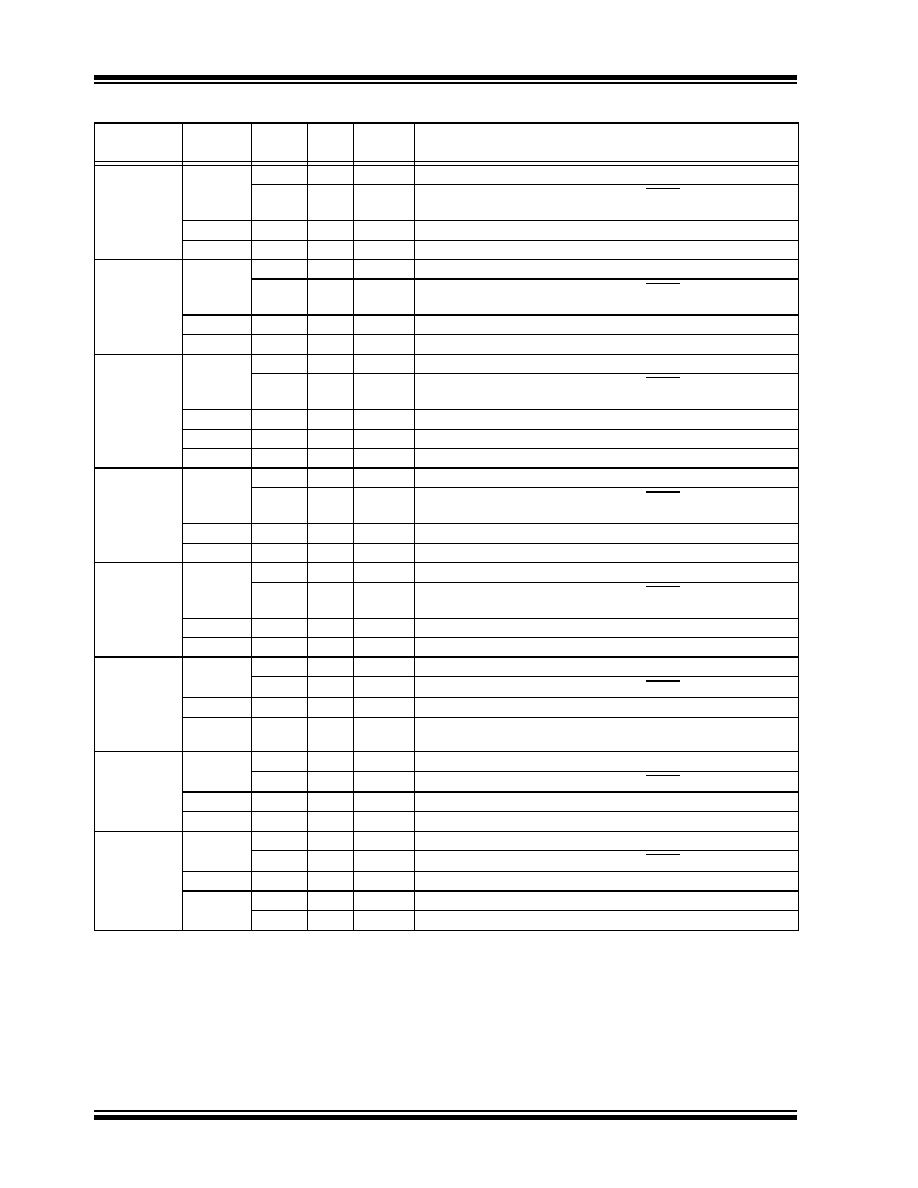
PIC18F2450/4450
DS39760A-page 102
Advance Information
� 2006 Microchip Technology Inc.
TABLE 9-3:
PORTB I/O SUMMARY
Pin
Function
TRIS
Setting
I/O
I/O Type
Description
RB0/AN12/
INT0
RB0
0
OUT
DIG
LATB<0> data output; not affected by analog input.
1
IN
TTL
PORTB<0> data input; weak pull-up when RBPU bit is cleared.
Disabled when analog input enabled.
(1)
AN12
1
IN
ANA
A/D input channel 12.
(1)
INT0
1
IN
ST
External interrupt 0 input.
RB1/AN10/
INT1
RB1
0
OUT
DIG
LATB<1> data output; not affected by analog input.
1
IN
TTL
PORTB<1> data input; weak pull-up when RBPU bit is cleared.
Disabled when analog input enabled.
(1)
AN10
1
IN
ANA
A/D input channel 10.
(1)
INT1
1
IN
ST
External interrupt 1 input.
RB2/AN8/
INT2/VMO
RB2
0
OUT
DIG
LATB<2> data output; not affected by analog input.
1
IN
TTL
PORTB<2> data input; weak pull-up when RBPU bit is cleared.
Disabled when analog input enabled.
(1)
AN8
1
IN
ANA
A/D input channel 8.
(1)
INT2
1
IN
ST
External interrupt 2 input.
VMO
0
OUT
DIG
External USB transceiver VMO data output.
RB3/AN9/VPO
RB3
0
OUT
DIG
LATB<3> data output; not affected by analog input.
1
IN
TTL
PORTB<3> data input; weak pull-up when RBPU bit is cleared.
Disabled when analog input enabled.
(1)
AN9
1
IN
ANA
A/D input channel 9.
(1)
VPO
0
OUT
DIG
External USB transceiver VPO data output.
RB4/AN11/
KBI0
RB4
0
OUT
DIG
LATB<4> data output; not affected by analog input.
1
IN
TTL
PORTB<4> data input; weak pull-up when RBPU bit is cleared.
Disabled when analog input enabled.
(1)
AN11
1
IN
ANA
A/D input channel 11.
(1)
KBI0
1
IN
TTL
Interrupt-on-pin change.
RB5/KBI1/
PGM
RB5
0
OUT
DIG
LATB<5> data output.
1
IN
TTL
PORTB<5> data input; weak pull-up when RBPU bit is cleared.
KBI1
1
IN
TTL
Interrupt-on-pin change.
PGM
x
IN
ST
Single-Supply Programming mode entry (ICSPTM). Enabled by LVP
Configuration bit; all other pin functions disabled.
RB6/KBI2/
PGC
RB6
0
OUT
DIG
LATB<6> data output.
1
IN
TTL
PORTB<6> data input; weak pull-up when RBPU bit is cleared.
KBI2
1
IN
TTL
Interrupt-on-pin change.
PGC
x
IN
ST
Serial execution (ICSP) clock input for ICSP and ICD operation.
(2)
RB7/KBI3/
PGD
RB7
0
OUT
DIG
LATB<7> data output.
1
IN
TTL
PORTB<7> data input; weak pull-up when RBPU bit is cleared.
KBI3
1
IN
TTL
Interrupt-on-pin change.
PGD
x
OUT
DIG
Serial execution data output for ICSP and ICD operation.
(2)
x
IN
ST
Serial execution data input for ICSP and ICD operation.
(2)
Legend:
OUT = Output, IN = Input, ANA = Analog Signal, DIG = Digital Output, ST = Schmitt Buffer Input,
TTL = TTL Buffer Input, x = Don't care (TRIS bit does not affect port direction or is overridden for this option)
Note
1:
Configuration on POR is determined by PBADEN Configuration bit. Pins are configured as analog inputs when
PBADEN is set and digital inputs when PBADEN is cleared.
2:
All other pin functions are disabled when ICSPTM or ICD operation is enabled.

PIC18F2450/4450
� 2006 Microchip Technology Inc.
Advance Information
DS39760A-page 103
TABLE 9-4:
SUMMARY OF REGISTERS ASSOCIATED WITH PORTB
Name
Bit 7
Bit 6
Bit 5
Bit 4
Bit 3
Bit 2
Bit 1
Bit 0
Reset
Values
on page
PORTB
RB7
RB6
RB5
RB4
RB3
RB2
RB1
RB0
51
LATB
LATB7
LATB6
LATB5
LATB4
LATB3
LATB2
LATB1
LATB0
51
TRISB
TRISB7
TRISB6
TRISB5
TRISB4
TRISB3
TRISB2
TRISB1
TRISB0
51
INTCON
GIE/GIEH PEIE/GIEL
TMR0IE
INT0IE
RBIE
TMR0IF
INT0IF
RBIF
49
INTCON2
RBPU
INTEDG0
INTEDG1 INTEDG2
--
TMR0IP
--
RBIP
49
INTCON3
INT2IP
INT1IP
--
INT2IE
INT1IE
--
INT2IF
INT1IF
49
ADCON1
--
--
VCFG1
VCFG0
PCFG3
PCFG2
PCFG1
PCFG0
50
UCON
--
PPBRST
SE0
PKTDIS
USBEN
RESUME SUSPND
--
52
Legend: -- = unimplemented, read as `0'. Shaded cells are not used by PORTB.

PIC18F2450/4450
DS39760A-page 104
Advance Information
� 2006 Microchip Technology Inc.
9.3
PORTC, TRISC and LATC
Registers
PORTC is a 7-bit wide, bidirectional port. The
corresponding data direction register is TRISC. Setting
a TRISC bit (= 1) will make the corresponding PORTC
pin an input (i.e., put the corresponding output driver in
a high-impedance mode). Clearing a TRISC bit (= 0)
will make the corresponding PORTC pin an output (i.e.,
put the contents of the output latch on the selected pin).
In PIC18F2450/4450 devices, the RC3 pin is not
implemented.
The Data Latch register (LATC) is also memory
mapped. Read-modify-write operations on the LATC
register read and write the latched output value for
PORTC.
PORTC is primarily multiplexed with serial
communication modules, including the EUSART and
the USB module (Table 9-5). Except for RC4 and RC5,
PORTC uses Schmitt Trigger input buffers.
Pins RC4 and RC5 are multiplexed with the USB
module. Depending on the configuration of the module,
they can serve as the differential data lines for the on-
chip USB transceiver, or the data inputs from an
external USB transceiver. Both RC4 and RC5 have
TTL input buffers instead of the Schmitt Trigger buffers
on the other pins.
Unlike other PORTC pins, RC4 and RC5 do not have
TRISC bits associated with them. As digital ports, they
can only function as digital inputs. When configured for
USB operation, the data direction is determined by the
configuration and status of the USB module at a given
time. If an external transceiver is used, RC4 and RC5
always function as inputs from the transceiver. If the
on-chip transceiver is used, the data direction is
determined by the operation being performed by the
module at that time.
When the external transceiver is enabled, RC2 also
serves as the output enable control to the transceiver.
Additional information on configuring USB options is
provided in Section 14.2.2.2 "External Transceiver".
When enabling peripheral functions on PORTC pins
other than RC4 and RC5, care should be taken in
defining the TRIS bits. Some peripherals override the
TRIS bit to make a pin an output, while other
peripherals override the TRIS bit to make a pin an
input. The user should refer to the corresponding
peripheral section for the correct TRIS bit settings.
The contents of the TRISC register are affected by
peripheral overrides. Reading TRISC always returns
the current contents, even though a peripheral device
may be overriding one or more of the pins.
EXAMPLE 9-3:
INITIALIZING PORTC
Note:
On a Power-on Reset, these pins, except
RC4 and RC5, are configured as digital
inputs. To use pins RC4 and RC5 as
digital inputs, the USB module must be
disabled (UCON<3> = 0) and the on-chip
USB transceiver must be disabled
(UCFG<3> = 1).
CLRF
PORTC
;
Initialize PORTC by
; clearing output
; data latches
CLRF
LATC
; Alternate method
; to clear output
; data latches
MOVLW
07h
;
Value used to
; initialize data
; direction
MOVWF
TRISC
;
RC<5:0> as outputs
;
RC<7:6> as inputs

PIC18F2450/4450
� 2006 Microchip Technology Inc.
Advance Information
DS39760A-page 105
TABLE 9-5:
PORTC I/O SUMMARY
Pin
Function
TRIS
Setting
I/O
I/O Type
Description
RC0/T1OSO/
T1CKI
RC0
0
OUT
DIG
LATC<0> data output.
1
IN
ST
PORTC<0> data input.
T1OSO
x
OUT
ANA
Timer1 oscillator output; enabled when Timer1 oscillator enabled.
Disables digital I/O.
T1CKI
1
IN
ST
Timer1 counter input.
RC1/T1OSI/
UOE
RC1
0
OUT
DIG
LATC<1> data output.
1
IN
ST
PORTC<1> data input.
T1OSI
x
IN
ANA
Timer1 oscillator input; enabled when Timer1 oscillator enabled.
Disables digital I/O.
UOE
0
OUT
DIG
External USB transceiver OE output.
RC2/CCP1
RC2
0
OUT
DIG
LATC<2> data output.
1
IN
ST
PORTC<2> data input.
CCP1
0
OUT
DIG
CCP1 Compare and PWM output; takes priority over port data.
1
IN
ST
CCP1 Capture input.
RC4/D-/VM
RC4
--
(1)
IN
TTL
PORTC<4> data input; disabled when USB module or on-chip
transceiver is enabled.
D-
--
(1)
OUT
XCVR
USB bus differential minus line output (internal transceiver).
--
(1)
IN
XCVR
USB bus differential minus line input (internal transceiver).
VM
--
(1)
IN
TTL
External USB transceiver VM input.
RC5/D+/VP
RC5
--
(1)
IN
TTL
PORTC<5> data input; disabled when USB module or on-chip
transceiver is enabled.
D+
--
(1)
OUT
XCVR
USB bus differential plus line output (internal transceiver).
--
1)
IN
XCVR
USB bus differential plus line input (internal transceiver).
VP
--
1)
IN
TTL
External USB transceiver VP input.
RC6/TX/CK
RC6
0
OUT
DIG
LATC<6> data output.
1
IN
ST
PORTC<6> data input.
TX
0
OUT
DIG
Asynchronous serial transmit data output (EUSART module); takes
priority over port data. User must configure as output.
CK
0
OUT
DIG
Synchronous serial clock output (EUSART module); takes priority
over port data.
1
IN
ST
Synchronous serial clock input (EUSART module).
RC7/RX/DT
RC7
0
OUT
DIG
LATC<7> data output.
1
IN
ST
PORTC<7> data input.
RX
1
IN
ST
Asynchronous serial receive data input (EUSART module).
DT
1
OUT
DIG
Synchronous serial data output (EUSART module).
1
IN
ST
Synchronous serial data input (EUSART module). User must
configure as an input.
Legend:
OUT = Output, IN = Input, ANA = Analog Signal, DIG = Digital Output, ST = Schmitt Buffer Input,
TTL = TTL Buffer Input, XCVR = USB Transceiver, x = Don't care (TRIS bit does not affect port direction or is
overridden for this option)
Note
1:
RC4 and RC5 do not have corresponding TRISC bits. In Port mode, these pins are input only. USB data direction is
determined by the USB configuration.

PIC18F2450/4450
DS39760A-page 106
Advance Information
� 2006 Microchip Technology Inc.
TABLE 9-6:
SUMMARY OF REGISTERS ASSOCIATED WITH PORTC
Name
Bit 7
Bit 6
Bit 5
Bit 4
Bit 3
Bit 2
Bit 1
Bit 0
Reset
Values
on page
PORTC
RC7
RC6
RC5
(1)
RC4
(1)
--
RC2
RC1
RC0
51
LATC
LATC7
LATC6
--
--
--
LATC2
LATC1
LATC0
51
TRISC
TRISC7
TRISC6
--
--
--
TRISC2
TRISC1
TRISC0
51
UCON
--
PPBRST
SE0
PKTDIS
USBEN
RESUME SUSPND
--
52
Legend: -- = unimplemented, read as `0'. Shaded cells are not used by PORTC.
Note 1:
RC5 and RC4 are only available as port pins when the USB module is disabled (UCON<3> = 0).

PIC18F2450/4450
� 2006 Microchip Technology Inc.
Advance Information
DS39760A-page 107
9.4
PORTD, TRISD and LATD
Registers
PORTD is an 8-bit wide, bidirectional port. The
corresponding data direction register is TRISD. Setting
a TRISD bit (= 1) will make the corresponding PORTD
pin an input (i.e., put the corresponding output driver in
a high-impedance mode). Clearing a TRISD bit (= 0)
will make the corresponding PORTD pin an output (i.e.,
put the contents of the output latch on the selected pin).
The Data Latch register (LATD) is also memory
mapped. Read-modify-write operations on the LATD
register read and write the latched output value for
PORTD.
All pins on PORTD are implemented with Schmitt
Trigger input buffers. Each pin is individually
configurable as an input or output.
EXAMPLE 9-4:
INITIALIZING PORTD
Note:
PORTD is only available on 40/44-pin
devices.
Note:
On a Power-on Reset, these pins are
configured as digital inputs.
CLRF
PORTD
;
Initialize PORTD by
; clearing output
; data latches
CLRF
LATD
; Alternate method
; to clear output
; data latches
MOVLW
0CFh
;
Value used to
; initialize data
; direction
MOVWF
TRISD
; Set RD<3:0> as inputs
;
RD<5:4> as outputs
;
RD<7:6> as inputs

PIC18F2450/4450
DS39760A-page 108
Advance Information
� 2006 Microchip Technology Inc.
TABLE 9-7:
PORTD I/O SUMMARY
TABLE 9-8:
SUMMARY OF REGISTERS ASSOCIATED WITH PORTD
Pin
Function
TRIS
Setting
I/O
I/O Type
Description
RD0
RD0
0
OUT
DIG
LATD<0> data output.
1
IN
ST
PORTD<0> data input.
RD1
RD1
0
OUT
DIG
LATD<1> data output.
1
IN
ST
PORTD<1> data input.
RD2
RD2
0
OUT
DIG
LATD<2> data output.
1
IN
ST
PORTD<2> data input.
RD3
RD3
0
OUT
DIG
LATD<3> data output.
1
IN
ST
PORTD<3> data input.
RD4
RD4
0
OUT
DIG
LATD<4> data output.
1
IN
ST
PORTD<4> data input.
RD5
RD5
0
OUT
DIG
LATD<5> data output
1
IN
ST
PORTD<5> data input
RD6
RD6
0
OUT
DIG
LATD<6> data output.
1
IN
ST
PORTD<6> data input.
RD7
RD7
0
OUT
DIG
LATD<7> data output.
1
IN
ST
PORTD<7> data input.
Legend:
OUT = Output, IN = Input, DIG = Digital Output, ST = Schmitt Buffer Input
Name
Bit 7
Bit 6
Bit 5
Bit 4
Bit 3
Bit 2
Bit 1
Bit 0
Reset
Values
on page
PORTD
(1)
RD7
RD6
RD5
RD4
RD3
RD2
RD1
RD0
51
LATD
(1)
LATD7
LATD6
LATD5
LATD4
LATD3
LATD2
LATD1
LATD0
51
TRISD
(1)
TRISD7
TRISD6
TRISD5
TRISD4
TRISD3
TRISD2
TRISD1
TRISD0
51
Note 1:
These registers and/or bits are unimplemented on 28-pin devices.

PIC18F2450/4450
� 2006 Microchip Technology Inc.
Advance Information
DS39760A-page 109
9.5
PORTE, TRISE and LATE
Registers
Depending on the particular PIC18F2450/4450 device
selected, PORTE is implemented in two different ways.
For 40/44-pin devices, PORTE is a 4-bit wide port.
Three pins (RE0/AN5, RE1/AN6 and RE2/AN7) are
individually configurable as inputs or outputs. These
pins have Schmitt Trigger input buffers. When selected
as an analog input, these pins will read as `0's.
The corresponding data direction register is TRISE.
Setting a TRISE bit (= 1) will make the corresponding
PORTE pin an input (i.e., put the corresponding output
driver in a high-impedance mode). Clearing a TRISE bit
(= 0) will make the corresponding PORTE pin an output
(i.e., put the contents of the output latch on the selected
pin).
TRISE controls the direction of the RE pins, even when
they are being used as analog inputs. The user must
make sure to keep the pins configured as inputs when
using them as analog inputs.
The Data Latch register (LATE) is also memory
mapped. Read-modify-write operations on the LATE
register read and write the latched output value for
PORTE.
The fourth pin of PORTE (MCLR/V
PP
/RE3) is an input
only pin. Its operation is controlled by the MCLRE Config-
uration bit. When selected as a port pin (MCLRE = 0), it
functions as a digital input only pin; as such, it does not
have TRIS or LAT bits associated with its operation.
Otherwise, it functions as the device's Master Clear input.
In either configuration, RE3 also functions as the
programming voltage input during programming.
EXAMPLE 9-5:
INITIALIZING PORTE
9.5.1
PORTE IN 28-PIN DEVICES
For 28-pin devices, PORTE is only available when
Master Clear functionality is disabled (MCLRE = 0). In
these cases, PORTE is a single bit, input only port
comprised of RE3 only. The pin operates as previously
described.
Note:
On a Power-on Reset, RE2:RE0 are
configured as analog inputs.
Note:
On a Power-on Reset, RE3 is enabled as
a digital input only if Master Clear
functionality is disabled.
CLRF
PORTE
; Initialize PORTE by
; clearing output
; data latches
CLRF
LATE
; Alternate method
; to clear output
; data latches
MOVLW
0Ah
; Configure A/D
MOVWF
ADCON1
; for digital inputs
MOVLW
03h
; Value used to
; initialize data
; direction
MOVWF
TRISC
; Set RE<0> as inputs
; RE<1> as inputs
; RE<2> as outputs
REGISTER 9-1:
PORTE REGISTER
U-0
U-0
U-0
U-0
R/W-x
R/W-0
R/W-0
R/W-0
--
--
--
--
RE3
(1,2)
RE2
(3)
RE1
(3)
RE0
(3)
bit 7
bit 0
Legend:
R = Readable bit
W = Writable bit
U = Unimplemented bit, read as `0'
-n = Value at POR
`1' = Bit is set
`0' = Bit is cleared
x = Bit is unknown
bit 7-4
Unimplemented: Read as `0'
bit 3-0
RE3:RE0: PORTE Data Input bits
(1,2,3)
Note 1:
implemented only when Master Clear functionality is disabled (MCLRE Configuration bit = 0); otherwise,
read as `0'.
2:
RE3 is the only PORTE bit implemented on both 28-pin and 40/44-pin devices. All other bits are
implemented only when PORTE is implemented (i.e., 40/44-pin devices).
3:
Unimplemented in 28-pin devices; read as `0'.
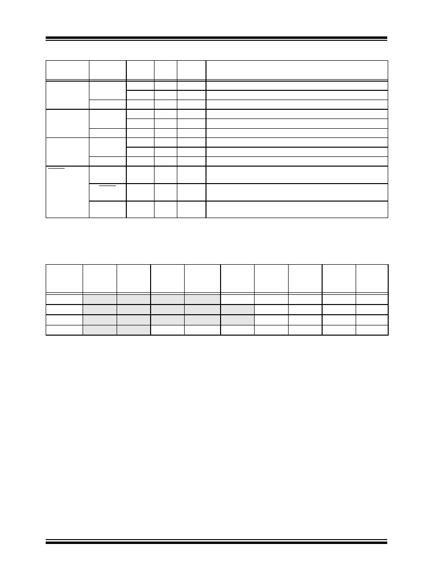
PIC18F2450/4450
DS39760A-page 110
Advance Information
� 2006 Microchip Technology Inc.
TABLE 9-9:
PORTE I/O SUMMARY
TABLE 9-10:
SUMMARY OF REGISTERS ASSOCIATED WITH PORTE
Pin
Function
TRIS
Setting
I/O
I/O Type
Description
RE0/AN5
RE0
0
OUT
DIG
LATE<0> data output; not affected by analog input.
1
IN
ST
PORTE<0> data input; disabled when analog input enabled.
AN5
1
IN
ANA
A/D input channel 5; default configuration on POR.
RE1/AN6
RE1
0
OUT
DIG
LATE<1> data output; not affected by analog input.
1
IN
ST
PORTE<1> data input; disabled when analog input enabled.
AN6
1
IN
ANA
A/D input channel 6; default configuration on POR.
RE2/AN7
RE2
0
OUT
DIG
LATE<2> data output; not affected by analog input.
1
IN
ST
PORTE<2> data input; disabled when analog input enabled.
AN7
1
IN
ANA
A/D input channel 7; default configuration on POR.
MCLR/V
PP
/
RE3
RE3
--
(1)
IN
ST
PORTE<3> data input; enabled when MCLRE Configuration bit
is clear.
MCLR
--
(1)
IN
ST
External Master Clear input; enabled when MCLRE Configuration bit
is set.
V
PP
--
(1)
IN
ANA
High-voltage detection, used for ICSPTM mode entry detection.
Always available regardless of pin mode.
Legend:
OUT = Output, IN = Input, ANA = Analog Signal, DIG = Digital Output, ST = Schmitt Buffer Input.
Note
1:
RE3 does not have a corresponding TRISE<3> bit. This pin is always an input regardless of mode.
Name
Bit 7
Bit 6
Bit 5
Bit 4
Bit 3
Bit 2
Bit 1
Bit 0
Reset
Values
on page
PORTE
--
--
--
--
RE3
(1,2)
RE2
(3)
RE1
(3)
RE0
(3)
51
LATE
(3)
--
--
--
--
--
LATE2
LATE1
LATE0
51
TRISE
(3)
--
--
--
--
--
TRISE2
TRISE1
TRISE0
51
ADCON1
--
--
VCFG1
VCFG0
PCFG3
PCFG2
PCFG1
PCFG0
50
Legend: -- = unimplemented, read as `0'
Note 1:
Implemented only when Master Clear functionality is disabled (MCLRE Configuration bit = 0); otherwise,
read as `0'.
2:
RE3 is the only PORTE bit implemented on both 28-pin and 40/44-pin devices. All other bits are
implemented only when PORTE is implemented (i.e., 40/44-pin devices).
3:
These registers and/or bits are unimplemented on 28-pin devices.

PIC18F2450/4450
� 2006 Microchip Technology Inc.
Advance Information
DS39760A-page 111
10.0
TIMER0 MODULE
The Timer0 module incorporates the following features:
� Software selectable operation as a timer or
counter in both 8-Bit or 16-Bit modes
� Readable and writable registers
� Dedicated 8-bit, software programmable
prescaler
� Selectable clock source (internal or external)
� Edge select for external clock
� Interrupt on overflow
The T0CON register (Register 10-1) controls all
aspects of the module's operation, including the
prescale selection. It is both readable and writable.
A simplified block diagram of the Timer0 module in
8-Bit mode is shown in Figure 10-1. Figure 10-2 shows
a simplified block diagram of the Timer0 module in 16-
Bit mode.
REGISTER 10-1:
T0CON: TIMER0 CONTROL REGISTER
R/W-1
R/W-1
R/W-1
R/W-1
R/W-1
R/W-1
R/W-1
R/W-1
TMR0ON
T08BIT
T0CS
T0SE
PSA
T0PS2
T0PS1
T0PS0
bit 7
bit 0
Legend:
R = Readable bit
W = Writable bit
U = Unimplemented bit, read as `0'
-n = Value at POR
`1' = Bit is set
`0' = Bit is cleared
x = Bit is unknown
bit 7
TMR0ON: Timer0 On/Off Control bit
1
= Enables Timer0
0
= Stops Timer0
bit 6
T08BIT: Timer0 8-Bit/16-Bit Control bit
1
= Timer0 is configured as an 8-bit timer/counter
0
= Timer0 is configured as a 16-bit timer/counter
bit 5
T0CS: Timer0 Clock Source Select bit
1
= Transition on T0CKI pin
0
= Internal instruction cycle clock (CLKO)
bit 4
T0SE: Timer0 Source Edge Select bit
1
= Increment on high-to-low transition on T0CKI pin
0
= Increment on low-to-high transition on T0CKI pin
bit 3
PSA: Timer0 Prescaler Assignment bit
1
= TImer0 prescaler is NOT assigned. Timer0 clock input bypasses prescaler.
0
= Timer0 prescaler is assigned. Timer0 clock input comes from prescaler output.
bit 2-0
T0PS2:T0PS0: Timer0 Prescaler Select bits
111
= 1:256 Prescale value
110
= 1:128 Prescale value
101
= 1:64 Prescale value
100
= 1:32 Prescale value
011
= 1:16 Prescale value
010
= 1:8 Prescale value
001
= 1:4 Prescale value
000
= 1:2 Prescale value
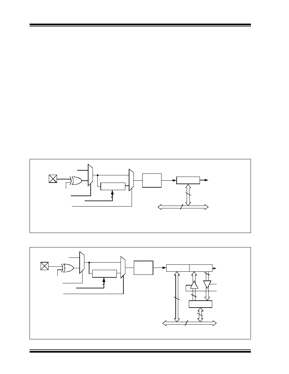
PIC18F2450/4450
DS39760A-page 112
Advance Information
� 2006 Microchip Technology Inc.
10.1
Timer0 Operation
Timer0 can operate as either a timer or a counter; the
mode is selected by clearing the T0CS bit
(T0CON<5>). In Timer mode, the module increments
on every clock by default unless a different prescaler
value is selected (see Section 10.3 "Prescaler"). If
the TMR0 register is written to, the increment is
inhibited for the following two instruction cycles. The
user can work around this by writing an adjusted value
to the TMR0 register.
The Counter mode is selected by setting the T0CS bit
(= 1). In Counter mode, Timer0 increments either on
every rising or falling edge of pin RA4/T0CKI. The
incrementing edge is determined by the Timer0 Source
Edge Select bit, T0SE (T0CON<4>); clearing this bit
selects the rising edge. Restrictions on the external
clock input are discussed below.
An external clock source can be used to drive Timer0;
however, it must meet certain requirements to ensure
that the external clock can be synchronized with the
internal phase clock (T
OSC
). There is a delay between
synchronization and the onset of incrementing the
timer/counter.
10.2
Timer0 Reads and Writes in
16-Bit Mode
TMR0H is not the actual high byte of Timer0 in 16-Bit
mode; it is actually a buffered version of the real high
byte of Timer0, which is not directly readable nor
writable (refer to Figure 10-2). TMR0H is updated with
the contents of the high byte of Timer0 during a read of
TMR0L. This provides the ability to read all 16 bits of
Timer0 without having to verify that the read of the high
and low byte were valid, due to a rollover between
successive reads of the high and low byte.
Similarly, a write to the high byte of Timer0 must also
take place through the TMR0H Buffer register. The high
byte is updated with the contents of TMR0H when a
write occurs to TMR0L. This allows all 16 bits of Timer0
to be updated at once.
FIGURE 10-1:
TIMER0 BLOCK DIAGRAM (8-BIT MODE)
FIGURE 10-2:
TIMER0 BLOCK DIAGRAM (16-BIT MODE)
Note:
Upon Reset, Timer0 is enabled in 8-Bit mode with clock input from T0CKI maximum prescale.
T0CKI pin
T0SE
0
1
1
0
T0CS
F
OSC
/4
Programmable
Prescaler
Sync with
Internal
Clocks
TMR0L
(2 T
CY
Delay)
Internal Data Bus
PSA
T0PS2:T0PS0
Set
TMR0IF
on Overflow
3
8
8
Note:
Upon Reset, Timer0 is enabled in 8-Bit mode with clock input from T0CKI maximum prescale.
T0CKI pin
T0SE
0
1
1
0
T0CS
F
OSC
/4
Programmable
Prescaler
Sync with
Internal
Clocks
TMR0L
(2 T
CY
Delay)
Internal Data Bus
8
PSA
T0PS2:T0PS0
Set
TMR0IF
on Overflow
3
TMR0
TMR0H
High Byte
8
8
8
Read TMR0L
Write TMR0L
8
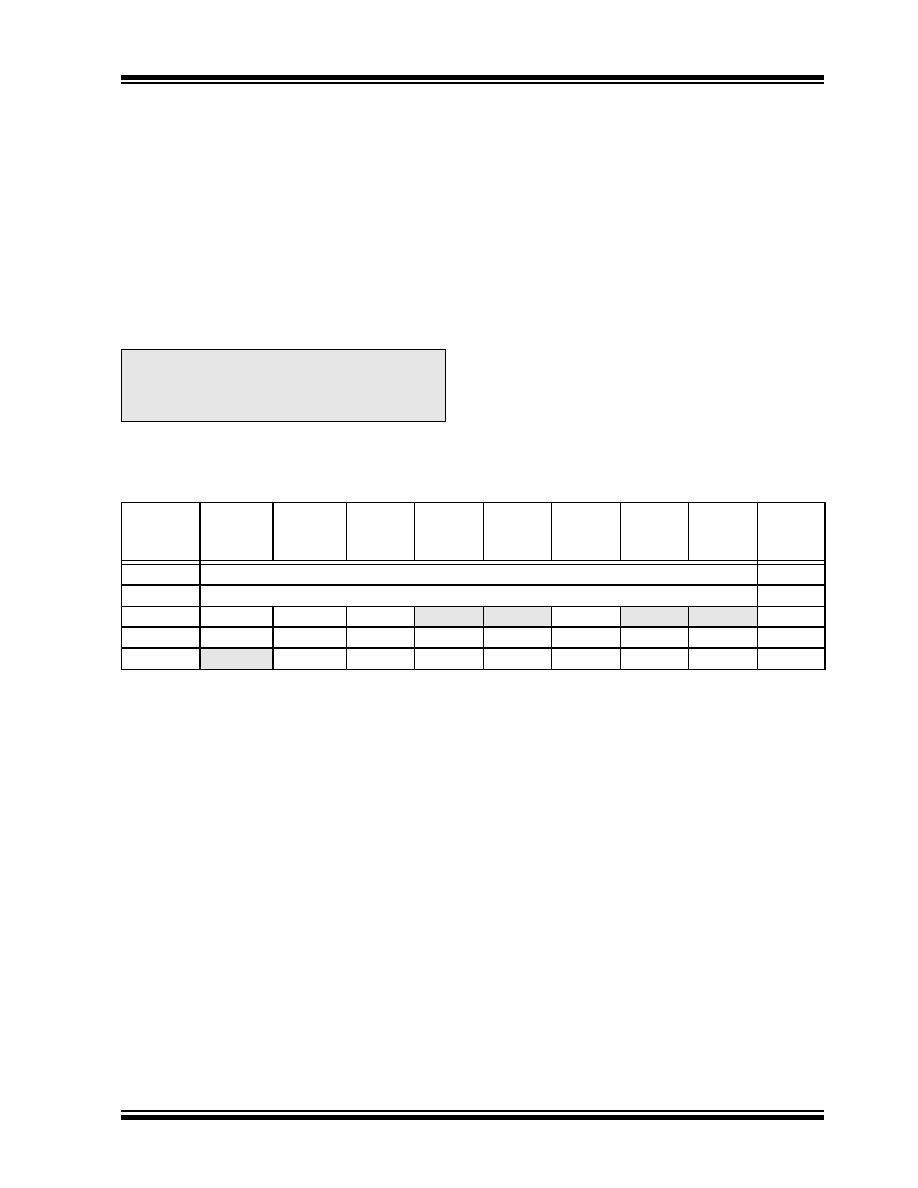
PIC18F2450/4450
� 2006 Microchip Technology Inc.
Advance Information
DS39760A-page 113
10.3
Prescaler
An 8-bit counter is available as a prescaler for the Timer0
module. The prescaler is not directly readable or writable;
its value is set by the PSA and T0PS2:T0PS0 bits
(T0CON<3:0>) which determine the prescaler
assignment and prescale ratio.
Clearing the PSA bit assigns the prescaler to the
Timer0 module. When it is assigned, prescale values
from 1:2 through 1:256, in power-of-2 increments, are
selectable.
When assigned to the Timer0 module, all instructions
writing to the TMR0 register (e.g., CLRF TMR0, MOVWF
TMR0, BSF TMR0,
etc.) clear the prescaler count.
10.3.1
SWITCHING PRESCALER
ASSIGNMENT
The prescaler assignment is fully under software
control and can be changed "on-the-fly" during program
execution.
10.4
Timer0 Interrupt
The TMR0 interrupt is generated when the TMR0
register overflows from FFh to 00h in 8-Bit mode, or
from FFFFh to 0000h in 16-Bit mode. This overflow
sets the TMR0IF flag bit. The interrupt can be masked
by clearing the TMR0IE bit (INTCON<5>). Before re-
enabling the interrupt, the TMR0IF bit must be cleared
in software by the Interrupt Service Routine.
Since Timer0 is shut down in Sleep mode, the TMR0
interrupt cannot awaken the processor from Sleep.
TABLE 10-1:
REGISTERS ASSOCIATED WITH TIMER0
Note:
Writing to TMR0 when the prescaler is
assigned to Timer0 will clear the prescaler
count but will not change the prescaler
assignment.
Name
Bit 7
Bit 6
Bit 5
Bit 4
Bit 3
Bit 2
Bit 1
Bit 0
Reset
Values
on page
TMR0L
Timer0 Register Low Byte
50
TMR0H
Timer0 Register High Byte
50
INTCON
GIE/GIEH PEIE/GIEL
TMR0IE
INT0IE
RBIE
TMR0IF
INT0IF
RBIF
49
T0CON
TMR0ON
T08BIT
T0CS
T0SE
PSA
T0PS2
T0PS1
T0PS0
50
TRISA
--
TRISA6
(1)
TRISA5
TRISA4
TRISA3
TRISA2
TRISA1
TRISA0
51
Legend: -- = unimplemented locations, read as `0'. Shaded cells are not used by Timer0.
Note 1:
RA6 is configured as a port pin based on various primary oscillator modes. When the port pin is disabled,
all of the associated bits read `0'.

PIC18F2450/4450
DS39760A-page 114
Advance Information
� 2006 Microchip Technology Inc.
NOTES:

PIC18F2450/4450
� 2006 Microchip Technology Inc.
Advance Information
DS39760A-page 115
11.0
TIMER1 MODULE
The Timer1 timer/counter module incorporates these
features:
� Software selectable operation as a 16-bit timer or
counter
� Readable and writable 8-bit registers (TMR1H
and TMR1L)
� Selectable clock source (internal or external) with
device clock or Timer1 oscillator internal options
� Interrupt on overflow
� Module Reset on CCP Special Event Trigger
� Device clock status flag (T1RUN)
A simplified block diagram of the Timer1 module is
shown in Figure 11-1. A block diagram of the module's
operation in Read/Write mode is shown in Figure 11-2.
The module incorporates its own low-power oscillator
to provide an additional clocking option. The Timer1
oscillator can also be used as a low-power clock source
for the microcontroller in power-managed operation.
Timer1 can also be used to provide Real-Time Clock
(RTC) functionality to applications with only a minimal
addition of external components and code overhead.
Timer1 is controlled through the T1CON Control
register (Register 11-1). It also contains the Timer1
Oscillator Enable bit (T1OSCEN). Timer1 can be
enabled or disabled by setting or clearing control bit,
TMR1ON (T1CON<0>).
REGISTER 11-1:
T1CON: TIMER1 CONTROL REGISTER
R/W-0
R-0
R/W-0
R/W-0
R/W-0
R/W-0
R/W-0
R/W-0
RD16
T1RUN
T1CKPS1
T1CKPS0
T1OSCEN
T1SYNC
TMR1CS
TMR1ON
bit 7
bit 0
Legend:
R = Readable bit
W = Writable bit
U = Unimplemented bit, read as `0'
-n = Value at POR
`1' = Bit is set
`0' = Bit is cleared
x = Bit is unknown
bit 7
RD16: 16-Bit Read/Write Mode Enable bit
1
= Enables register read/write of Timer1 in one 16-bit operation
0
= Enables register read/write of Timer1 in two 8-bit operations
bit 6
T1RUN: Timer1 System Clock Status bit
1
= Device clock is derived from Timer1 oscillator
0
= Device clock is derived from another source
bit 5-4
T1CKPS1:T1CKPS0: Timer1 Input Clock Prescale Select bits
11
= 1:8 Prescale value
10
= 1:4 Prescale value
01
= 1:2 Prescale value
00
= 1:1 Prescale value
bit 3
T1OSCEN: Timer1 Oscillator Enable bit
1
= Timer1 oscillator is enabled
0
= Timer1 oscillator is shut off
The oscillator inverter and feedback resistor are turned off to eliminate power drain.
bit 2
T1SYNC: Timer1 External Clock Input Synchronization Select bit
When TMR1CS = 1:
1
= Do not synchronize external clock input
0
= Synchronize external clock input
When TMR1CS = 0:
This bit is ignored. Timer1 uses the internal clock when TMR1CS = 0.
bit 1
TMR1CS: Timer1 Clock Source Select bit
1
= External clock from RC0/T1OSO/T1CKI pin (on the rising edge)
0
= Internal clock (F
OSC
/4)
bit 0
TMR1ON: Timer1 On bit
1
= Enables Timer1
0
= Stops Timer1
PIC18F2450/4450
DS39760A-page 116
Advance Information
� 2006 Microchip Technology Inc.
11.1
Timer1 Operation
Timer1 can operate in one of these modes:
� Timer
� Synchronous Counter
� Asynchronous Counter
The operating mode is determined by the clock select
bit, TMR1CS (T1CON<1>). When TMR1CS is cleared
(= 0), Timer1 increments on every internal instruction
cycle (F
OSC
/4). When the bit is set, Timer1 increments
on every rising edge of the Timer1 external clock input
or the Timer1 oscillator, if enabled.
When Timer1 is enabled, the RC1/T1OSI/UOE and
RC0/T1OSO/T1CKI pins become inputs. This means
the values of TRISC<1:0> are ignored and the pins are
read as `0'.
FIGURE 11-1:
TIMER1 BLOCK DIAGRAM
FIGURE 11-2:
TIMER1 BLOCK DIAGRAM (16-BIT READ/WRITE MODE)
T1SYNC
TMR1CS
T1CKPS1:T1CKPS0
Sleep Input
T1OSCEN
(1)
F
OSC
/4
Internal
Clock
On/Off
Prescaler
1, 2, 4, 8
Synchronize
Detect
1
0
2
T1OSO/T1CKI
T1OSI
1
0
TMR1ON
TMR1L
Set
TMR1IF
on Overflow
TMR1
High Byte
Clear TMR1
(CCP Special Event Trigger)
Timer1 Oscillator
Note 1: When enable bit, T1OSCEN, is cleared, the inverter and feedback resistor are turned off to eliminate power drain.
On/Off
Timer1
T1SYNC
TMR1CS
T1CKPS1:T1CKPS0
Sleep Input
T1OSCEN
(1)
F
OSC
/4
Internal
Clock
Prescaler
1, 2, 4, 8
Synchronize
Detect
1
0
2
T1OSO/T1CKI
T1OSI
Note 1: When enable bit, T1OSCEN, is cleared, the inverter and feedback resistor are turned off to eliminate power drain.
1
0
TMR1L
Internal Data Bus
8
Set
TMR1IF
on Overflow
TMR1
TMR1H
High Byte
8
8
8
Read TMR1L
Write TMR1L
8
TMR1ON
Clear TMR1
(CCP Special Event Trigger)
Timer1 Oscillator
On/Off
Timer1
PIC18F2450/4450
� 2006 Microchip Technology Inc.
Advance Information
DS39760A-page 117
11.2
Timer1 16-Bit Read/Write Mode
Timer1 can be configured for 16-bit reads and writes
(see Figure 11-2). When the RD16 control bit
(T1CON<7>) is set, the address for TMR1H is mapped
to a buffer register for the high byte of Timer1. A read
from TMR1L will load the contents of the high byte of
Timer1 into the Timer1 high byte buffer. This provides
the user with the ability to accurately read all 16 bits of
Timer1 without having to determine whether a read of
the high byte, followed by a read of the low byte, has
become invalid due to a rollover between reads.
A write to the high byte of Timer1 must also take place
through the TMR1H Buffer register. The Timer1 high
byte is updated with the contents of TMR1H when a
write occurs to TMR1L. This allows a user to write all
16 bits to both the high and low bytes of Timer1 at once.
The high byte of Timer1 is not directly readable or
writable in this mode. All reads and writes must take
place through the Timer1 High Byte Buffer register.
Writes to TMR1H do not clear the Timer1 prescaler.
The prescaler is only cleared on writes to TMR1L.
11.3
Timer1 Oscillator
An on-chip crystal oscillator circuit is incorporated
between pins T1OSI (input) and T1OSO (amplifier
output). It is enabled by setting the Timer1 Oscillator
Enable bit, T1OSCEN (T1CON<3>). The oscillator is a
low-power circuit rated for 32 kHz crystals. It will
continue to run during all power-managed modes. The
circuit for a typical LP oscillator is shown in Figure 11-3.
Table 11-1 shows the capacitor selection for the Timer1
oscillator.
The user must provide a software time delay to ensure
proper start-up of the Timer1 oscillator.
FIGURE 11-3:
EXTERNAL
COMPONENTS FOR THE
TIMER1 LP OSCILLATOR
TABLE 11-1:
CAPACITOR SELECTION FOR
THE TIMER OSCILLATOR
(2,3,4)
11.3.1
USING TIMER1 AS A CLOCK
SOURCE
The Timer1 oscillator is also available as a clock source
in power-managed modes. By setting the clock select
bits, SCS1:SCS0 (OSCCON<1:0>), to `01', the device
switches to SEC_RUN mode. Both the CPU and
peripherals are clocked from the Timer1 oscillator. If the
IDLEN bit (OSCCON<7>) is cleared and a SLEEP
instruction is executed, the device enters SEC_IDLE
mode. Additional details are available in Section 3.0
"Power-Managed Modes".
Whenever the Timer1 oscillator is providing the clock
source, the Timer1 system clock status flag, T1RUN
(T1CON<6>), is set. This can be used to determine the
controller's current clocking mode. It can also indicate
the clock source being currently used by the Fail-Safe
Clock Monitor. If the Clock Monitor is enabled and the
Timer1 oscillator fails while providing the clock, polling
the T1RUN bit will indicate whether the clock is being
provided by the Timer1 oscillator or another source.
11.3.2
LOW-POWER TIMER1 OPTION
The Timer1 oscillator can operate at two distinct levels
of power consumption based on device configuration.
When the LPT1OSC Configuration bit is set, the Timer1
oscillator operates in a low-power mode. When
LPT1OSC is not set, Timer1 operates at a higher power
level. Power consumption for a particular mode is
relatively constant, regardless of the device's operating
mode. The default Timer1 configuration is the higher
power mode.
As the low-power Timer1 mode tends to be more
sensitive to interference, high noise environments may
cause some oscillator instability. The low-power option
is, therefore, best suited for low noise applications
where power conservation is an important design
consideration.
Note:
See the Notes with Table 11-1 for additional
information about capacitor selection.
C1
C2
XTAL
PIC18FXXXX
T1OSI
T1OSO
32.768 kHz
33 pF
33 pF
Osc Type
Freq
C1
C2
LP
32 kHz
27 pF
(1)
27 pF
(1)
Note 1: Microchip suggests these values as a
starting point in validating the oscillator
circuit.
2: Higher capacitance increases the stability
of the oscillator but also increases the
start-up time.
3: Since each resonator/crystal has its own
characteristics, the user should consult
the resonator/crystal manufacturer for
appropriate values of external
components.
4: Capacitor values are for design guidance
only.
PIC18F2450/4450
DS39760A-page 118
Advance Information
� 2006 Microchip Technology Inc.
11.3.3
TIMER1 OSCILLATOR LAYOUT
CONSIDERATIONS
The Timer1 oscillator circuit draws very little power
during operation. Due to the low-power nature of the
oscillator, it may also be sensitive to rapidly changing
signals in close proximity.
The oscillator circuit, shown in Figure 11-3, should be
located as close as possible to the microcontroller.
There should be no circuits passing within the oscillator
circuit boundaries other than V
SS
or V
DD
.
If a high-speed circuit must be located near the oscilla-
tor (such as the CCP1 pin in Output Compare or PWM
mode, or the primary oscillator using the OSC2 pin), a
grounded guard ring around the oscillator circuit, as
shown in Figure 11-4, may be helpful when used on a
single-sided PCB or in addition to a ground plane.
FIGURE 11-4:
OSCILLATOR CIRCUIT
WITH GROUNDED
GUARD RING
11.4
Timer1 Interrupt
The TMR1 register pair (TMR1H:TMR1L) increments
from 0000h to FFFFh and rolls over to 0000h. The
Timer1 interrupt, if enabled, is generated on overflow
which is latched in interrupt flag bit, TMR1IF
(PIR1<0>). This interrupt can be enabled or disabled
by setting or clearing the Timer1 Interrupt Enable bit,
TMR1IE (PIE1<0>).
11.5
Resetting Timer1 Using the CCP
Special Event Trigger
If the CCP module is configured in Compare mode
to generate a Special Event Trigger
(CCP1M3:CCP1M0 = 1011), this signal will reset
Timer1. The trigger from CCP1 will also start an A/D
conversion if the A/D module is enabled (see
Section 13.3.4 "Special Event Trigger" for more
information).
The module must be configured as either a timer or a
synchronous counter to take advantage of this feature.
When used this way, the CCPRH:CCPRL register pair
effectively becomes a period register for Timer1.
If Timer1 is running in Asynchronous Counter mode,
this Reset operation may not work.
In the event that a write to Timer1 coincides with a
Special Event Trigger, the write operation will take
precedence.
11.6
Using Timer1 as a Real-Time
Clock
Adding an external LP oscillator to Timer1 (such as the
one described in Section 11.3 "Timer1 Oscillator")
gives users the option to include RTC functionality to
their applications. This is accomplished with an
inexpensive watch crystal to provide an accurate time
base and several lines of application code to calculate
the time. When operating in Sleep mode and using a
battery or supercapacitor as a power source, it can
completely eliminate the need for a separate RTC
device and battery backup.
The application code routine, RTCisr, shown in
Example 11-1, demonstrates a simple method to
increment a counter at one-second intervals using an
Interrupt Service Routine. Incrementing the TMR1
register pair to overflow triggers the interrupt and calls
the routine which increments the seconds counter by
one. Additional counters for minutes and hours are
incremented as the previous counter overflows.
Since the register pair is 16 bits wide, counting up to
overflow the register directly from a 32.768 kHz clock
would take 2 seconds. To force the overflow at the
required one-second intervals, it is necessary to
preload it. The simplest method is to set the MSb of
TMR1H with a BSF instruction. Note that the TMR1L
register is never preloaded or altered; doing so may
introduce cumulative error over many cycles.
For this method to be accurate, Timer1 must operate in
Asynchronous mode and the Timer1 overflow interrupt
must be enabled (PIE1<0> = 1) as shown in the
routine, RTCinit. The Timer1 oscillator must also be
enabled and running at all times.
V
DD
OSC1
V
SS
OSC2
RC0
RC1
RC2
Note: Not drawn to scale.
Note:
The Special Event Triggers from the
CCP1 module will not set the TMR1IF
interrupt flag bit (PIR1<0>).
PIC18F2450/4450
� 2006 Microchip Technology Inc.
Advance Information
DS39760A-page 119
EXAMPLE 11-1:
IMPLEMENTING A REAL-TIME CLOCK USING A TIMER1 INTERRUPT SERVICE
TABLE 11-2:
REGISTERS ASSOCIATED WITH TIMER1 AS A TIMER/COUNTER
RTCinit
MOVLW
80h
; Preload TMR1 register pair
MOVWF
TMR1H
; for 1 second overflow
CLRF
TMR1L
MOVLW
b'00001111'
; Configure for external clock,
MOVWF
T1OSC
; Asynchronous operation, external oscillator
CLRF
secs
; Initialize timekeeping registers
CLRF
mins
;
MOVLW
d'12'
MOVWF
hours
BSF
PIE1, TMR1IE
; Enable Timer1 interrupt
RETURN
RTCisr
BSF
TMR1H, 7
; Preload for 1 sec overflow
BCF
PIR1, TMR1IF
; Clear interrupt flag
INCF
secs, F
; Increment seconds
MOVLW
d'59'
; 60 seconds elapsed?
CPFSGT
secs
RETURN
; No, done
CLRF
secs
; Clear seconds
INCF
mins, F
; Increment minutes
MOVLW
d'59'
; 60 minutes elapsed?
CPFSGT
mins
RETURN
; No, done
CLRF
mins
; clear minutes
INCF
hours, F
; Increment hours
MOVLW
d'23'
; 24 hours elapsed?
CPFSGT
hours
RETURN
; No, done
MOVLW
d'01'
; Reset hours to 1
MOVWF
hours
RETURN
; Done
Name
Bit 7
Bit 6
Bit 5
Bit 4
Bit 3
Bit 2
Bit 1
Bit 0
Reset
Values
on page
INTCON
GIE/GIEH PEIE/GIEL
TMR0IE
INT0IE
RBIE
TMR0IF
INT0IF
RBIF
49
PIR1
--
ADIF
RCIF
TXIF
--
CCP1IF
TMR2IF
TMR1IF
51
PIE1
--
ADIE
RCIE
TXIE
--
CCP1IE
TMR2IE
TMR1IE
51
IPR1
--
ADIP
RCIP
TXIP
--
CCP1IP
TMR2IP
TMR1IP
51
TMR1L
Timer1 Register Low Byte
50
TMR1H
TImer1 Register High Byte
50
T1CON
RD16
T1RUN
T1CKPS1 T1CKPS0 T1OSCEN T1SYNC
TMR1CS
TMR1ON
50
Legend: -- = unimplemented, read as `0'. Shaded cells are not used by the Timer1 module.

PIC18F2450/4450
DS39760A-page 120
Advance Information
� 2006 Microchip Technology Inc.
NOTES:

PIC18F2450/4450
� 2006 Microchip Technology Inc.
Advance Information
DS39760A-page 121
12.0
TIMER2 MODULE
The Timer2 module timer incorporates the following
features:
� 8-bit timer and period registers (TMR2 and PR2,
respectively)
� Readable and writable (both registers)
� Software programmable prescaler (1:1, 1:4 and
1:16)
� Software programmable postscaler (1:1 through
1:16)
� Interrupt on TMR2 to PR2 match
The module is controlled through the T2CON register
(Register 12-1) which enables or disables the timer and
configures the prescaler and postscaler. Timer2 can be
shut off by clearing control bit, TMR2ON (T2CON<2>),
to minimize power consumption.
A simplified block diagram of the module is shown in
Figure 12-1.
12.1
Timer2 Operation
In normal operation, TMR2 is incremented from 00h on
each clock (F
OSC
/4). A 2-bit counter/prescaler on the
clock input gives direct input, divide-by-4 and divide-by-
16 prescale options. These are selected by the prescaler
control bits, T2CKPS1:T2CKPS0 (T2CON<1:0>). The
value of TMR2 is compared to that of the period register,
PR2, on each clock cycle. When the two values match,
the comparator generates a match signal as the timer
output. This signal also resets the value of TMR2 to 00h
on the next cycle and drives the output counter/
postscaler (see Section 12.2 "Timer2 Interrupt").
The TMR2 and PR2 registers are both directly readable
and writable. The TMR2 register is cleared on any
device Reset, while the PR2 register initializes at FFh.
Both the prescaler and postscaler counters are cleared
on the following events:
� a write to the TMR2 register
� a write to the T2CON register
� any device Reset (Power-on Reset, MCLR Reset,
Watchdog Timer Reset or Brown-out Reset)
TMR2 is not cleared when T2CON is written.
REGISTER 12-1:
T2CON: TIMER2 CONTROL REGISTER
U-0
R/W-0
R/W-0
R/W-0
R/W-0
R/W-0
R/W-0
R/W-0
--
T2OUTPS3
T2OUTPS2
T2OUTPS1
T2OUTPS0
TMR2ON
T2CKPS1
T2CKPS0
bit 7
bit 0
Legend:
R = Readable bit
W = Writable bit
U = Unimplemented bit, read as `0'
-n = Value at POR
`1' = Bit is set
`0' = Bit is cleared
x = Bit is unknown
bit 7
Unimplemented: Read as `0'
bit 6-3
T2OUTPS3:T2OUTPS0: Timer2 Output Postscale Select bits
0000
= 1:1 Postscale
0001
= 1:2 Postscale
�
�
�
1111
= 1:16 Postscale
bit 2
TMR2ON: Timer2 On bit
1
= Timer2 is on
0
= Timer2 is off
bit 1-0
T2CKPS1:T2CKPS0: Timer2 Clock Prescale Select bits
00
= Prescaler is 1
01
= Prescaler is 4
1x
= Prescaler is 16
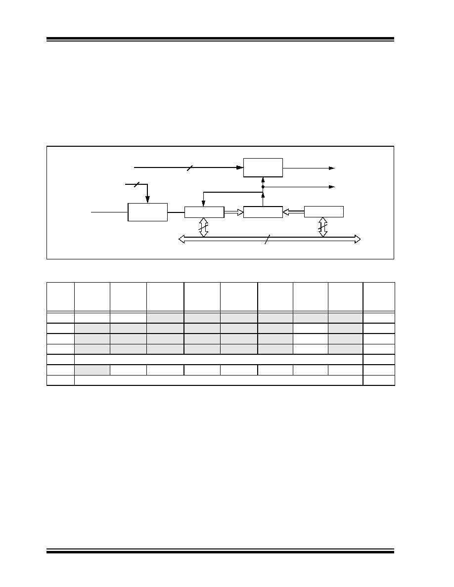
PIC18F2450/4450
DS39760A-page 122
Advance Information
� 2006 Microchip Technology Inc.
12.2
Timer2 Interrupt
Timer2 also can generate an optional device interrupt.
The Timer2 output signal (TMR2 to PR2 match)
provides the input for the 4-bit output counter/
postscaler. This counter generates the TMR2 match
interrupt flag which is latched in TMR2IF (PIR1<1>).
The interrupt is enabled by setting the TMR2 Match
Interrupt Enable bit, TMR2IE (PIE1<1>).
A range of 16 postscale options (from 1:1 through 1:16
inclusive) can be selected with the postscaler control
bits, T2OUTPS3:T2OUTPS0 (T2CON<6:3>).
12.3
TMR2 Output
The unscaled output of TMR2 is available primarily to
the CCP module, where it is used as a time base for
operations in PWM mode.
FIGURE 12-1:
TIMER2 BLOCK DIAGRAM
TABLE 12-1:
REGISTERS ASSOCIATED WITH TIMER2 AS A TIMER/COUNTER
Name
Bit 7
Bit 6
Bit 5
Bit 4
Bit 3
Bit 2
Bit 1
Bit 0
Reset
Values
on page
INTCON GIE/GIEH
PEIE/GIEL
TMR0IE
INT0IE
RBIE
TMR0IF
INT0IF
RBIF
49
PIR1
--
ADIF
RCIF
TXIF
--
CCP1IF
TMR2IF
TMR1IF
51
PIE1
--
ADIE
RCIE
TXIE
--
CCP1IE
TMR2IE
TMR1IE
51
IPR1
--
ADIP
RCIP
TXIP
--
CCP1IP
TMR2IP
TMR1IP
51
TMR2
Timer2 Register
50
T2CON
--
T2OUTPS3 T2OUTPS2 T2OUTPS1 T2OUTPS0 TMR2ON
T2CKPS1 T2CKPS0
50
PR2
Timer2 Period Register
50
Legend: -- = unimplemented, read as `0'. Shaded cells are not used by the Timer2 module.
Comparator
TMR2 Output
TMR2
Postscaler
Prescaler
PR2
2
F
OSC
/4
1:1 to 1:16
1:1, 1:4, 1:16
4
T2OUTPS3:T2OUTPS0
T2CKPS1:T2CKPS0
Set TMR2IF
Internal Data Bus
8
Reset
TMR2/PR2
8
8
(to PWM)
Match

PIC18F2450/4450
� 2006 Microchip Technology Inc.
Advance Information
DS39760A-page 123
13.0
CAPTURE/COMPARE/PWM
(CCP) MODULE
PIC18F2450/4450 devices have one CCP (Capture/
Compare/PWM) module. The module contains a 16-bit
register, which can operate as a 16-bit Capture register,
a 16-bit Compare register or a PWM Master/Slave Duty
Cycle register.
REGISTER 13-1:
CCP1CON: CAPTURE/COMPARE/PWM CONTROL REGISTER
U-0
U-0
R/W-0
R/W-0
R/W-0
R/W-0
R/W-0
R/W-0
--
--
DC1B1
DC1B0
CCP1M3
CCP1M2
CCP1M1
CCP1M0
bit 7
bit 0
Legend:
R = Readable bit
W = Writable bit
U = Unimplemented bit, read as `0'
-n = Value at POR
`1' = Bit is set
`0' = Bit is cleared
x = Bit is unknown
bit 7-6
Unimplemented: Read as `0'
bit 5-4
DC1B1:DC1B0: PWM Duty Cycle for CCP Module bits
Capture mode:
Unused.
Compare mode:
Unused.
PWM mode:
These bits are the two LSbs (bit 1 and bit 0) of the 10-bit PWM duty cycle. The eight MSbs of the duty
cycle are found in CCPR1L.
bit 3-0
CCP1M3:CCP1M0: CCP Module Mode Select bits
0000
= Capture/Compare/PWM disabled (resets CCP module)
0001
= Reserved
0010
= Compare mode: toggle output on match (CCP1IF bit is set)
0011
= Reserved
0100
= Capture mode: every falling edge
0101
= Capture mode: every rising edge
0110
= Capture mode: every 4th rising edge
0111
= Capture mode: every 16th rising edge
1000
= Compare mode: initialize CCP1 pin low; on compare match, force CCP1 pin high
(CCP1IF bit is set)
1001
= Compare mode: initialize CCP1 pin high; on compare match, force CCP1 pin low
(CCP1IF bit is set)
1010
= Compare mode: generate software interrupt on compare match (CCP1IF bit is set,
CCP1 pin reflects I/O state)
1011
= Compare mode: trigger special event, reset timer and start A/D conversion on CCP1 match
(CCP1IF bit is set)
11xx
= PWM mode
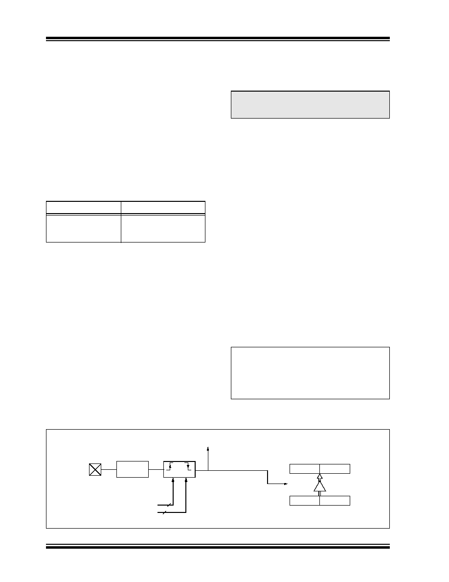
PIC18F2450/4450
DS39760A-page 124
Advance Information
� 2006 Microchip Technology Inc.
13.1
CCP Module Configuration
The Capture/Compare/PWM module is associated with
a control register (generically, CCP1CON) and a data
register (CCPR1). The data register, in turn, is
comprised of two 8-bit registers: CCPR1L (low byte)
and CCPR1H (high byte). All registers are both
readable and writable.
13.1.1
CCP MODULE AND TIMER
RESOURCES
The CCP module utilizes Timer1 or Timer2, depending
on the mode selected. Timer1 is available to the mod-
ule in Capture or Compare modes, while Timer2 is
available for modules in PWM mode.
TABLE 13-1:
CCP MODE � TIMER
RESOURCE
In Timer1 in Asynchronous Counter mode, the capture
operation will not work.
13.2
Capture Mode
In Capture mode, the CCPR1H:CCPR1L register pair
captures the 16-bit value of the TMR1 register when an
event occurs on the corresponding CCP1 pin. An event
is defined as one of the following:
� every falling edge
� every rising edge
� every 4th rising edge
� every 16th rising edge
The event is selected by the mode select bits,
CCP1M3:CCP1M0 (CCP1CON<3:0>). When a capture
is made, the interrupt request flag bit, CCP1IF, is set; it
must be cleared in software. If another capture occurs
before the value in register CCPR1 is read, the old
captured value is overwritten by the new captured value.
13.2.1
CCP1 PIN CONFIGURATION
In Capture mode, the CCP1 pin should be configured
as an input by setting the corresponding TRIS direction
bit.
13.2.2
SOFTWARE INTERRUPT
When the Capture mode is changed, a false capture
interrupt may be generated. The user should keep the
CCP1IE interrupt enable bit clear to avoid false
interrupts. The interrupt flag bit, CCP1IF, should also
be cleared following any such change in operating
mode.
13.2.3
CCP PRESCALER
There are four prescaler settings in Capture mode.
They are specified as part of the operating mode
selected by the mode select bits (CCP1M3:CCP1M0).
Whenever the CCP module is turned off or Capture
mode is disabled, the prescaler counter is cleared. This
means that any Reset will clear the prescaler counter.
Switching from one capture prescaler to another may
generate an interrupt. Also, the prescaler counter will
not be cleared, therefore, the first capture may be from
a non-zero prescaler. Example 13-1 shows the
recommended method for switching between capture
prescalers. This example also clears the prescaler
counter and will not generate the "false" interrupt.
EXAMPLE 13-1:
CHANGING BETWEEN
CAPTURE PRESCALERS
(CCP1 SHOWN)
FIGURE 13-1:
CAPTURE MODE OPERATION BLOCK DIAGRAM
CCP Mode
Timer Resource
Capture
Compare
PWM
Timer1
Timer1
Timer2
Note:
If RC2/CCP1 is configured as an output, a
write to the port can cause a capture
condition.
CLRF
CCP1CON
; Turn CCP module off
MOVLW
NEW_CAPT_PS
; Load WREG with the
; new prescaler mode
; value and CCP ON
MOVWF
CCP1CON
; Load CCP1CON with
; this value
CCPR1H
CCPR1L
TMR1H
TMR1L
Set CCP1IF
Q1:Q4
CCP1CON<3:0>
CCP1 pin
Prescaler
� 1, 4, 16
and
Edge Detect
TMR1
Enable
4
4
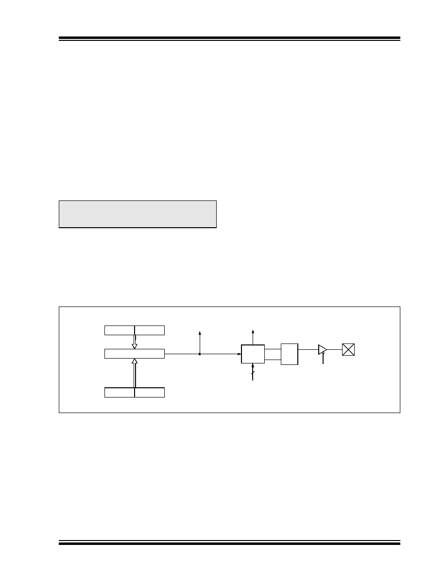
PIC18F2450/4450
� 2006 Microchip Technology Inc.
Advance Information
DS39760A-page 125
13.3
Compare Mode
In Compare mode, the 16-bit CCPR1 register value is
constantly compared against the TMR1 register pair
value. When a match occurs, the CCP1 pin can be:
� driven high
� driven low
� toggled (high-to-low or low-to-high)
� remain unchanged (that is, reflects the state of the
I/O latch)
The action on the pin is based on the value of the mode
select bits (CCP1M3:CCP1M0). At the same time, the
interrupt flag bit, CCP1IF, is set.
13.3.1
CCP1 PIN CONFIGURATION
The user must configure the CCP1 pin as an output by
clearing the appropriate TRIS bit.
13.3.2
TIMER1 MODE SELECTION
Timer1 must be running in Timer mode, or
Synchronized Counter mode, if the CCP module is
using the compare feature. In Asynchronous Counter
mode, the compare operation may not work.
13.3.3
SOFTWARE INTERRUPT MODE
When the Generate Software Interrupt mode is chosen
(CCP1M3:CCP1M0 = 1010), the CCP1 pin is not
affected. Only a CCP interrupt is generated, if enabled,
and the CCP1IE bit is set.
13.3.4
SPECIAL EVENT TRIGGER
The CCP module is equipped with a Special Event
Trigger. This is an internal hardware signal generated
in Compare mode to trigger actions by other modules.
The Special Event Trigger is enabled by selecting
the Compare Special Event Trigger mode
(CCP1M3:CCP1M0 = 1011).
For the CCP module, the Special Event Trigger resets
the Timer1 register pair. This allows the CCPR1
registers to serve as a programmable period register
for the Timer1.
The Special Event Trigger for CCP1 can also start an
A/D conversion. In order to do this, the A/D converter
must already be enabled.
FIGURE 13-2:
COMPARE MODE OPERATION BLOCK DIAGRAM
Note:
Clearing the CCP1CON register will force
the RC2 compare output latch to the
default low level.
CCPR1H
CCPR1L
TMR1H
TMR1L
Comparator
Q
S
R
Output
Logic
Special Event Trigger
Set CCP1IF
CCP1 pin
TRIS
CCP1CON<3:0>
Output Enable
Compare
4
(Timer1 Reset)
Match
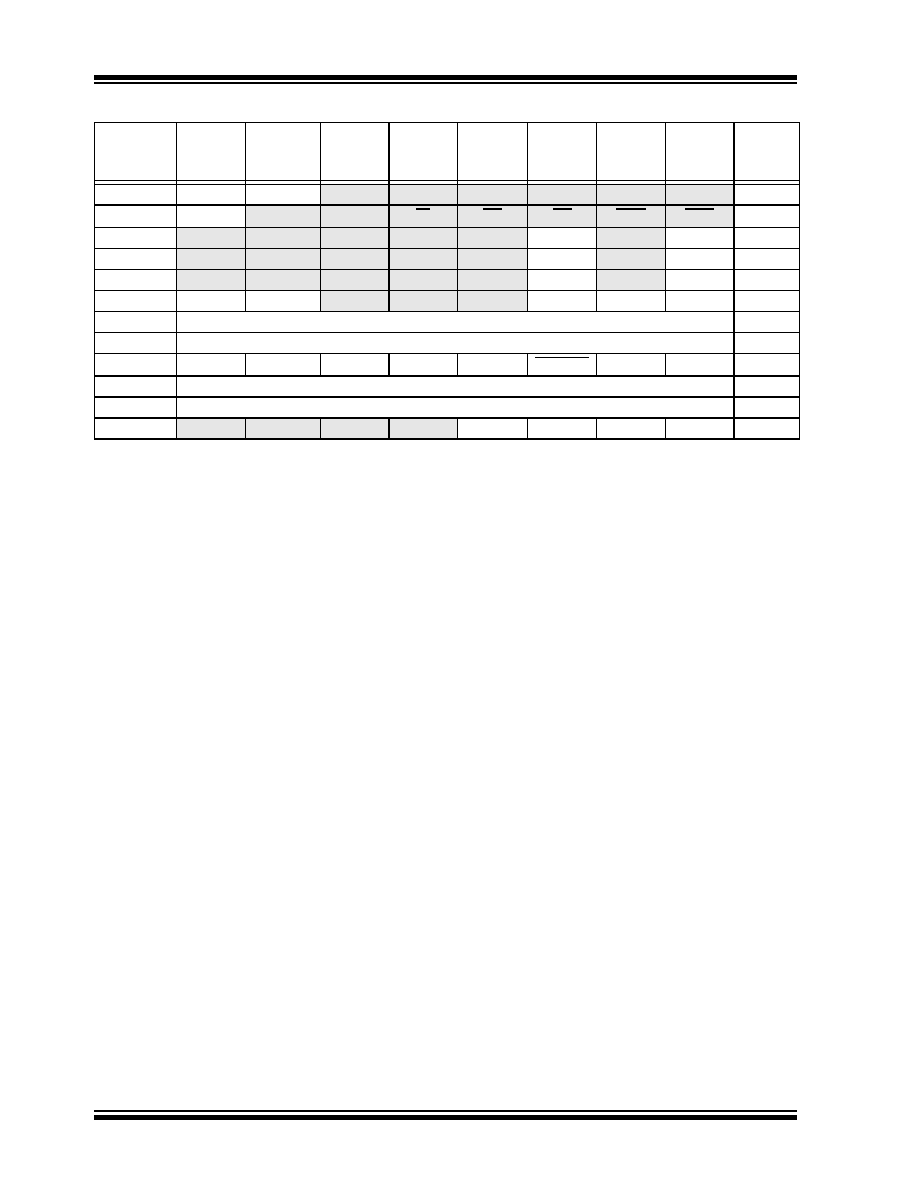
PIC18F2450/4450
DS39760A-page 126
Advance Information
� 2006 Microchip Technology Inc.
TABLE 13-2:
REGISTERS ASSOCIATED WITH CAPTURE, COMPARE, TIMER1
Name
Bit 7
Bit 6
Bit 5
Bit 4
Bit 3
Bit 2
Bit 1
Bit 0
Reset
Values
on page
INTCON
GIE/GIEH PEIE/GIEL
TMR0IE
INT0IE
RBIE
TMR0IF
INT0IF
RBIF
49
RCON
IPEN
SBOREN
(1)
--
RI
TO
PD
POR
BOR
50
PIR1
--
ADIF
RCIF
TXIF
--
CCP1IF
TMR2IF
TMR1IF
51
PIE1
--
ADIE
RCIE
TXIE
--
CCP1IE
TMR2IE
TMR1IE
51
IPR1
--
ADIP
RCIP
TXIP
--
CCP1IP
TMR2IP
TMR1IP
51
TRISC
TRISC7
TRISC6
--
--
--
TRISC2
TRISC1
TRISC0
51
TMR1L
Timer1 Register Low Byte
50
TMR1H
Timer1 Register High Byte
50
T1CON
RD16
T1RUN
T1CKPS1 T1CKPS0 T1OSCEN T1SYNC
TMR1CS
TMR1ON
50
CCPR1L
Capture/Compare/PWM Register 1 Low Byte
50
CCPR1H
Capture/Compare/PWM Register 1 High Byte
50
CCP1CON
--
--
DC1B1
DC1B0
CCP1M3
CCP1M2
CCP1M1
CCP1M0
50
Legend: -- = unimplemented, read as `0'. Shaded cells are not used by Capture/Compare and Timer1.
Note 1:
The SBOREN bit is only available when BOREN<1:0> = 01; otherwise, the bit reads as `0'.
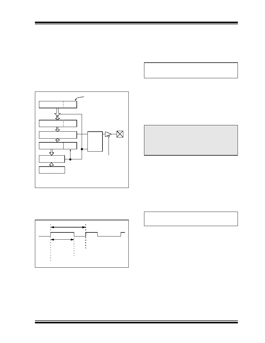
PIC18F2450/4450
� 2006 Microchip Technology Inc.
Advance Information
DS39760A-page 127
13.4
PWM Mode
In Pulse-Width Modulation (PWM) mode, the CCP1 pin
produces up to a 10-bit resolution PWM output.
Figure 13-3 shows a simplified block diagram of the
CCP module in PWM mode.
For a step-by-step procedure on how to set up the CCP
module for PWM operation, see Section 13.4.3
"Setup for PWM Operation".
FIGURE 13-3:
SIMPLIFIED PWM BLOCK
DIAGRAM
A PWM output (Figure 13-4) has a time base (period)
and a time that the output stays high (duty cycle).
The frequency of the PWM is the inverse of the
period (1/period).
FIGURE 13-4:
PWM OUTPUT
13.4.1
PWM PERIOD
The PWM period is specified by writing to the PR2
register. The PWM period can be calculated using the
following formula:
EQUATION 13-1:
PWM frequency is defined as 1/[PWM period].
When TMR2 is equal to PR2, the following three events
occur on the next increment cycle:
� TMR2 is cleared
� The CCP1 pin is set (exception: if PWM duty
cycle = 0%, the CCP1 pin will not be set)
� The PWM duty cycle is latched from CCPR1L into
CCPR1H
13.4.2
PWM DUTY CYCLE
The PWM duty cycle is specified by writing to the
CCPR1L register and to the CCP1CON<5:4> bits. Up
to 10-bit resolution is available. The CCPR1L contains
the eight MSbs and the CCP1CON<5:4> bits contain
the two LSbs. This 10-bit value is represented by
CCPR1L:CCP1CON<5:4>. The following equation is
used to calculate the PWM duty cycle in time:
EQUATION 13-2:
CCPR1L and CCP1CON<5:4> can be written to at any
time, but the duty cycle value is not latched into
CCPR1H until after a match between PR2 and TMR2
occurs (i.e., the period is complete). In PWM mode,
CCPR1H is a read-only register.
CCPR1L
CCPR1H (Slave)
Comparator
TMR2
Comparator
PR2
(Note 1)
R
Q
S
Duty Cycle Registers
CCP1CON<5:4>
Clear Timer,
CCP1 pin and
latch D.C.
Note 1: The 8-bit TMR2 value is concatenated with the 2-bit
internal Q clock, or 2 bits of the prescaler, to create
the 10-bit time base.
CCP1
Corresponding
TRIS bit
Output
Period
Duty Cycle
TMR2 = PR2
TMR2 = Duty Cycle
TMR2 = PR2
Note:
The Timer2 postscalers (see Section 12.0
"Timer2 Module") are not used in the
determination of the PWM frequency. The
postscaler could be used to have a servo
update rate at a different frequency than
the PWM output.
PWM Period = [(PR2) + 1] � 4 � T
OSC
�
(TMR2 Prescale Value)
PWM Duty Cycle = (CCPR1L:CCP1CON<5:4>) �
T
OSC
� (TMR2 Prescale Value)
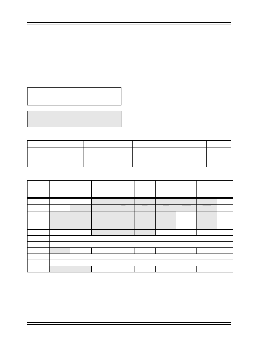
PIC18F2450/4450
DS39760A-page 128
Advance Information
� 2006 Microchip Technology Inc.
The CCPR1H register and a 2-bit internal latch are
used to double-buffer the PWM duty cycle. This
double-buffering is essential for glitchless PWM
operation.
When the CCPR1H and 2-bit latch match TMR2,
concatenated with an internal 2-bit Q clock or 2 bits of
the TMR2 prescaler, the CCP1 pin is cleared.
The maximum PWM resolution (bits) for a given PWM
frequency is given by the equation:
EQUATION 13-3:
13.4.3
SETUP FOR PWM OPERATION
The following steps should be taken when configuring
the CCP module for PWM operation:
1.
Set the PWM period by writing to the PR2
register.
2.
Set the PWM duty cycle by writing to the
CCPR1L register and CCP1CON<5:4> bits.
3.
Make the CCP1 pin an output by clearing the
appropriate TRIS bit.
4.
Set the TMR2 prescale value, then enable
Timer2 by writing to T2CON.
5.
Configure the CCP module for PWM operation.
TABLE 13-3:
EXAMPLE PWM FREQUENCIES AND RESOLUTIONS AT 40 MHz
TABLE 13-4:
REGISTERS ASSOCIATED WITH PWM AND TIMER2
Note:
If the PWM duty cycle value is longer than
the PWM period, the CCP1 pin will not be
cleared.
F
OSC
F
PWM
---------------
log
2
( )
log
-----------------------------bits
=
PWM Resolution (max)
PWM Frequency
2.44 kHz
9.77 kHz
39.06 kHz
156.25 kHz
312.50 kHz
416.67 kHz
Timer Prescaler (1, 4, 16)
16
4
1
1
1
1
PR2 Value
FFh
FFh
FFh
3Fh
1Fh
17h
Maximum Resolution (bits)
10
10
10
8
7
6.58
Name
Bit 7
Bit 6
Bit 5
Bit 4
Bit 3
Bit 2
Bit 1
Bit 0
Reset
Values
on page
INTCON
GIE/GIEH PEIE/GIEL
TMR0IE
INT0IE
RBIE
TMR0IF
INT0IF
RBIF
49
RCON
IPEN
SBOREN
(1)
--
RI
TO
PD
POR
BOR
50
PIR1
--
ADIF
RCIF
TXIF
--
CCP1IF
TMR2IF
TMR1IF
51
PIE1
--
ADIE
RCIE
TXIE
--
CCP1IE
TMR2IE
TMR1IE
51
IPR1
--
ADIP
RCIP
TXIP
--
CCP1IP
TMR2IP
TMR1IP
51
TRISC
TRISC7
TRISC6
--
--
--
TRISC2
TRISC1
TRISC0
51
TMR2
Timer2 Register
50
PR2
Timer2 Period Register
50
T2CON
--
T2OUTPS3 T2OUTPS2 T2OUTPS1 T2OUTPS0 TMR2ON
T2CKPS1
T2CKPS0
50
CCPR1L
Capture/Compare/PWM Register 1 Low Byte
50
CCPR1H
Capture/Compare/PWM Register 1 High Byte
50
CCP1CON
--
--
DC1B1
DC1B0
CCP1M3
CCP1M2
CCP1M1
CCP1M0
50
Legend: -- = unimplemented, read as `0'. Shaded cells are not used by PWM or Timer2.
Note 1:
The SBOREN bit is only available when BOREN<1:0> = 01; otherwise, the bit reads as `0'.
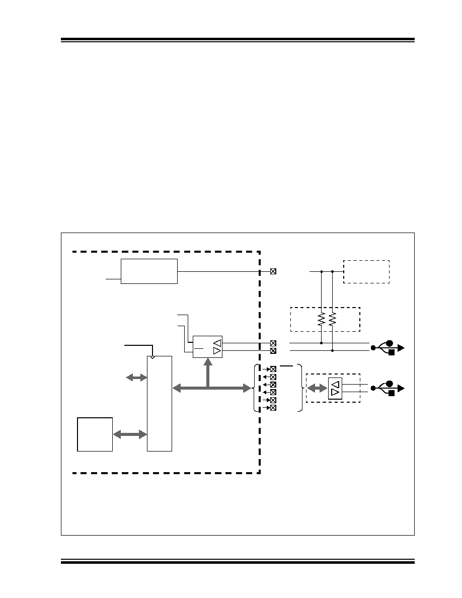
PIC18F2450/4450
� 2006 Microchip Technology Inc.
Advance Information
DS39760A-page 129
14.0
UNIVERSAL SERIAL BUS
(USB)
This section describes the details of the USB peripheral.
Because of the very specific nature of the module,
knowledge of USB is expected. Some high-level USB
information is provided in Section 14.9 "Overview of
USB" only for application design reference. Designers
are encouraged to refer to the official specification
published by the USB Implementers Forum (USB-IF) for
the latest information. USB Specification Revision 2.0 is
the most current specification at the time of publication
of this document.
14.1
Overview of the USB Peripheral
The PIC18F2450/4450 device family contains a full-
speed and low-speed compatible USB Serial Interface
Engine (SIE) that allows fast communication between
any USB host and the PIC
�
microcontroller. The SIE can
be interfaced directly to the USB, utilizing the internal
transceiver, or it can be connected through an external
transceiver. An internal 3.3V regulator is also available
to power the internal transceiver in 5V applications.
Some special hardware features have been included to
improve performance. Dual port memory in the
device's data memory space (USB RAM) has been
supplied to share direct memory access between the
microcontroller core and the SIE. Buffer descriptors are
also provided, allowing users to freely program
endpoint memory usage within the USB RAM space.
Figure 14-1 presents a general overview of the USB
peripheral and its features.
FIGURE 14-1:
USB PERIPHERAL AND OPTIONS
UOE
(1)
256-Byte
USB RAM
USB
SIE
USB Control and
VM
(1)
VP
(1)
RCV
(1)
VMO
(1)
VPO
(1)
Transceiver
External
Transceiver
EN
3.3V Regulator
D+
D-
OE
V
USB
External 3.3V
Supply
(3)
FSEN
UTRDIS
USB Clock from the
Oscillator Module
Configuration
VREGEN
External
Pull-ups
(2)
(Low
(Full
PIC18F2450/4450 Family
USB Bus
USB Bus
FS
Speed)
Speed)
Note 1:
This signal is only available if the internal transceiver is disabled (UTRDIS = 1).
2:
The pull-ups can be supplied either from the V
USB
pin or from an external 3.3V supply.
3:
Do not enable the internal regulator when using an external 3.3V supply.

PIC18F2450/4450
DS39760A-page 130
Advance Information
� 2006 Microchip Technology Inc.
14.2
USB Status and Control
The operation of the USB module is configured and
managed through three control registers. In addition, a
total of 22 registers are used to manage the actual USB
transactions. The registers are:
� USB Control register (UCON)
� USB Configuration register (UCFG)
� USB Transfer Status register (USTAT)
� USB Device Address register (UADDR)
� Frame Number registers (UFRMH:UFRML)
� Endpoint Enable registers 0 through 15 (UEPn)
14.2.1
USB CONTROL REGISTER (UCON)
The USB Control register (Register 14-1) contains bits
needed to control the module behavior during transfers.
The register contains bits that control the following:
� Main USB Peripheral Enable
� Ping-Pong Buffer Pointer Reset
� Control of the Suspend mode
� Packet Transfer Disable
In addition, the USB Control register contains a status
bit, SE0 (UCON<5>), which is used to indicate the
occurrence of a single-ended zero on the bus. When
the USB module is enabled, this bit should be
monitored to determine whether the differential data
lines have come out of a single-ended zero condition.
This helps to differentiate the initial power-up state from
the USB Reset signal.
The overall operation of the USB module is controlled
by the USBEN bit (UCON<3>). Setting this bit activates
the module and resets all of the PPBI bits in the Buffer
Descriptor Table to `0'. This bit also activates the on-
chip voltage regulator, if enabled. Thus, this bit can be
used as a soft attach/detach to the USB. Although all
status and control bits are ignored when this bit is clear,
the module needs to be fully preconfigured prior to
setting this bit.
REGISTER 14-1:
UCON: USB CONTROL REGISTER
U-0
R/W-0
R-x
R/C-0
R/W-0
R/W-0
R/W-0
U-0
--
PPBRST
SE0
PKTDIS
USBEN
RESUME
SUSPND
--
bit 7
bit 0
Legend:
C = Clearable bit
R = Readable bit
W = Writable bit
U = Unimplemented bit, read as `0'
-n = Value at POR
`1' = Bit is set
`0' = Bit is cleared
x = Bit is unknown
bit 7
Unimplemented: Read as `0'
bit 6
PPBRST: Ping-Pong Buffers Reset bit
1
= Reset all Ping-Pong Buffer Pointers to the Even Buffer Descriptor (BD) banks
0
= Ping-Pong Buffer Pointers not being reset
bit 5
SE0: Live Single-Ended Zero Flag bit
1
= Single-ended zero active on the USB bus
0
= No single-ended zero detected
bit 4
PKTDIS: Packet Transfer Disable bit
1
= SIE token and packet processing disabled, automatically set when a SETUP token is received
0
= SIE token and packet processing enabled
bit 3
USBEN: USB Module Enable bit
1
= USB module and supporting circuitry enabled (device attached)
0
= USB module and supporting circuitry disabled (device detached)
bit 2
RESUME: Resume Signaling Enable bit
1
= Resume signaling activated
0
= Resume signaling disabled
bit 1
SUSPND: Suspend USB bit
1
= USB module and supporting circuitry in Power Conserve mode, SIE clock inactive
0
= USB module and supporting circuitry in normal operation, SIE clock clocked at the configured rate
bit 0
Unimplemented: Read as `0'
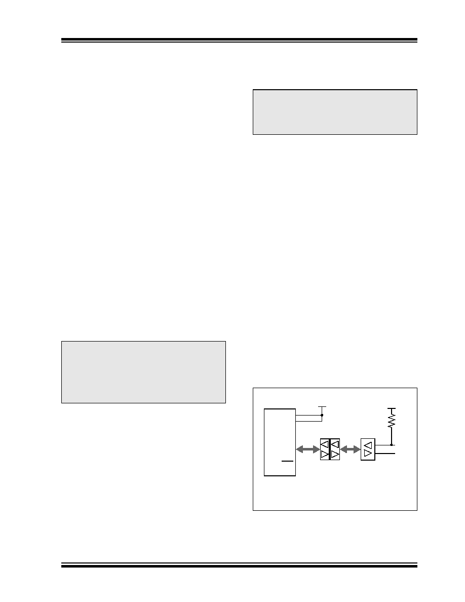
PIC18F2450/4450
� 2006 Microchip Technology Inc.
Advance Information
DS39760A-page 131
The PPBRST bit (UCON<6>) controls the Reset status
when Double-Buffering mode (ping-pong buffering) is
used. When the PPBRST bit is set, all Ping-Pong
Buffer Pointers are set to the Even buffers. PPBRST
has to be cleared by firmware. This bit is ignored in
buffering modes not using ping-pong buffering.
The PKTDIS bit (UCON<4>) is a flag indicating that the
SIE has disabled packet transmission and reception.
This bit is set by the SIE when a SETUP token is
received to allow setup processing. This bit cannot be
set by the microcontroller, only cleared; clearing it
allows the SIE to continue transmission and/or
reception. Any pending events within the Buffer
Descriptor Table will still be available, indicated within
the USTAT register's FIFO buffer.
The RESUME bit (UCON<2>) allows the peripheral to
perform a remote wake-up by executing Resume
signaling. To generate a valid remote wake-up,
firmware must set RESUME for 10 ms and then clear
the bit. For more information on Resume signaling, see
Sections 7.1.7.5, 11.4.4 and 11.9 in the USB 2.0
specification.
The SUSPND bit (UCON<1>) places the module and
supporting circuitry (i.e., voltage regulator) in a low-
power mode. The input clock to the SIE is also
disabled. This bit should be set by the software in
response to an IDLEIF interrupt. It should be reset by
the microcontroller firmware after an ACTVIF interrupt
is observed. When this bit is active, the device remains
attached to the bus but the transceiver outputs remain
Idle. The voltage on the V
USB
pin may vary depending
on the value of this bit. Setting this bit before a IDLEIF
request will result in unpredictable bus behavior.
14.2.2
USB CONFIGURATION REGISTER
(UCFG)
Prior to communicating over USB, the module's
associated internal and/or external hardware must be
configured. Most of the configuration is performed with
the UCFG register (Register 14-2). The separate USB
voltage regulator (see Section 14.2.2.7 "Internal
Regulator") is controlled through the Configuration
registers.
The UFCG register contains most of the bits that
control the system level behavior of the USB module.
These include:
� Bus Speed (full speed versus low speed)
� On-Chip Transceiver Enable
� Ping-Pong Buffer Usage
The UCFG register also contains two bits which aid in
module testing, debugging and USB certifications.
These bits control output enable state monitoring and
eye pattern generation.
14.2.2.1
Internal Transceiver
The USB peripheral has a built-in, USB 2.0, full-speed
and low-speed compliant transceiver, internally con-
nected to the SIE. This feature is useful for low-cost
single chip applications. The UTRDIS bit (UCFG<3>)
controls the transceiver; it is enabled by default
(UTRDIS = 0). The FSEN bit (UCFG<2>) controls the
transceiver speed; setting the bit enables full-speed
operation.
The USB specification requires 3.3V operation for
communications; however, the rest of the chip may be
running at a higher voltage. Thus, the transceiver is
supplied power from a separate source, V
USB
.
14.2.2.2
External Transceiver
This module provides support for use with an off-chip
transceiver. The off-chip transceiver is intended for
applications where physical conditions dictate the
location of the transceiver to be away from the SIE. For
example, applications that require isolation from the
USB could use an external transceiver through some
isolation to the microcontroller's SIE (Figure 14-2).
External transceiver operation is enabled by setting the
UTRDIS bit.
FIGURE 14-2:
TYPICAL EXTERNAL
TRANSCEIVER WITH
ISOLATION
Note:
While in Suspend mode, a typical bus
powered USB device is limited to 500
A
of current. This is the complete current
drawn by the PICmicro device and its sup-
porting circuitry. Care should be taken to
assure minimum current draw when the
device enters Suspend mode.
Note:
The USB speed, transceiver and pull-up
should only be configured during the mod-
ule setup phase. It is not recommended to
switch these settings while the module is
enabled.
PIC
�
Microcontroller
Transceiver
VPO
UOE
Note:
The above setting shows a simplified schematic
for a full-speed configuration using an external
transceiver with isolation.
VP
RCV
VMO
VM
D+
D-
Isolation
1.5 k
3.3V Derived
from USB
V
USB
V
DD
V
DD
Isolated
from USB

PIC18F2450/4450
DS39760A-page 132
Advance Information
� 2006 Microchip Technology Inc.
There are 6 signals from the module to communicate
with and control an external transceiver:
� VM: Input from the single-ended D- line
� VP: Input from the single-ended D+ line
� RCV: Input from the differential receiver
� VMO: Output to the differential line driver
� VPO: Output to the differential line driver
� UOE: Output enable
The VPO and VMO signals are outputs from the SIE to
the external transceiver. The RCV signal is the output
from the external transceiver to the SIE; it represents
the differential signals from the serial bus translated
into a single pulse train. The VM and VP signals are
used to report conditions on the serial bus to the SIE
that can't be captured with the RCV signal. The
combinations of states of these signals and their
interpretation are listed in Table 14-1 and Table 14-2.
REGISTER 14-2:
UCFG: USB CONFIGURATION REGISTER
R/W-0
R/W-0
U-0
R/W-0
R/W-0
R/W-0
R/W-0
R/W-0
UTEYE
UOEMON
(1)
--
UPUEN
(2,3)
UTRDIS
(2)
FSEN
(2)
PPB1
PPB0
bit 7
bit 0
Legend:
R = Readable bit
W = Writable bit
U = Unimplemented bit, read as `0'
-n = Value at POR
`1' = Bit is set
`0' = Bit is cleared
x = Bit is unknown
bit 7
UTEYE: USB Eye Pattern Test Enable bit
1
= Eye pattern test enabled
0
= Eye pattern test disabled
bit 6
UOEMON: USB OE Monitor Enable bit
(1)
1
= UOE signal active; it indicates intervals during which the D+/D- lines are driving
0
= UOE signal inactive
bit 5
Unimplemented: Read as `0'
bit 4
UPUEN: USB On-Chip Pull-up Enable bit
(2,3)
1
= On-chip pull-up enabled (pull-up on D+ with FSEN = 1 or D- with FSEN = 0)
0
= On-chip pull-up disabled
bit 3
UTRDIS: On-Chip Transceiver Disable bit
(2)
1
= On-chip transceiver disabled; digital transceiver interface enabled
0
= On-chip transceiver active
bit 2
FSEN: Full-Speed Enable bit
(2)
1
= Full-speed device: controls transceiver edge rates; requires input clock at 48 MHz
0
= Low-speed device: controls transceiver edge rates; requires input clock at 6 MHz
bit 1-0
PPB1:PPB0: Ping-Pong Buffers Configuration bits
11
= Enabled for all endpoints except Endpoint 0
10
= Even/Odd ping-pong buffers enabled for all endpoints
01
= Even/Odd ping-pong buffer enabled for OUT Endpoint 0
00
= Even/Odd ping-pong buffers disabled
Note 1:
If UTRDIS is set, the UOE signal will be active independent of the UOEMON bit setting.
2:
The UPUEN, UTRDIS and FSEN bits should never be changed while the USB module is enabled. These
values must be preconfigured prior to enabling the module.
3:
This bit is only valid when the on-chip transceiver is active (UTRDIS = 0); otherwise, it is ignored.
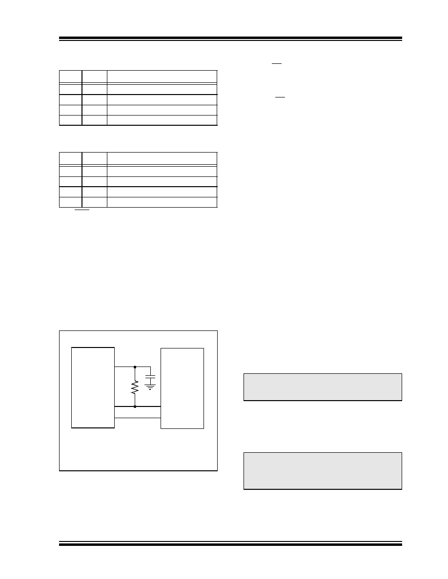
PIC18F2450/4450
� 2006 Microchip Technology Inc.
Advance Information
DS39760A-page 133
TABLE 14-1:
DIFFERENTIAL OUTPUTS TO
TRANSCEIVER
TABLE 14-2:
SINGLE-ENDED INPUTS
FROM TRANSCEIVER
The UOE signal toggles the state of the external
transceiver. This line is pulled low by the device to
enable the transmission of data from the SIE to an
external device.
14.2.2.3
Pull-up Resistors
The PIC18F2450/4450 devices require an external pull-
up resistor to meet the requirements for low-speed and
full-speed USB. Either an external 3.3V supply or the
V
USB
pin may be used to pull up D+ or D-. The pull-up
resistor must be 1.5 k
(�5%) as required by the USB
specifications. Figure 14-3 shows an example with the
V
USB
pin.
FIGURE 14-3:
EXTERNAL CIRCUITRY
14.2.2.4
Ping-Pong Buffer Configuration
The usage of ping-pong buffers is configured using the
PPB1:PPB0 bits. Refer to Section 14.4.4 "Ping-Pong
Buffering" for a complete explanation of the ping-pong
buffers.
14.2.2.5
USB Output Enable Monitor
The USB OE monitor provides indication as to whether
the SIE is listening to the bus or actively driving the bus.
This is enabled by default when using an external
transceiver or when UCFG<6> = 1.
The USB OE monitoring is useful for initial system
debugging, as well as scope triggering during eye
pattern generation tests.
14.2.2.6
Eye Pattern Test Enable
An automatic eye pattern test can be generated by the
module when the UCFG<7> bit is set. The eye pattern
output will be observable based on module settings,
meaning that the user is first responsible for configuring
the SIE clock settings, pull-up resistor and Transceiver
mode. In addition, the module has to be enabled.
Once UTEYE is set, the module emulates a switch from
a receive to transmit state and will start transmitting a
J-K-J-K bit sequence (K-J-K-J for full speed). The
sequence will be repeated indefinitely while the Eye
Pattern Test mode is enabled.
Note that this bit should never be set while the module
is connected to an actual USB system. This test mode
is intended for board verification to aid with USB
certification tests. It is intended to show a system
developer the noise integrity of the USB signals which
can be affected by board traces, impedance
mismatches and proximity to other system
components. It does not properly test the transition
from a receive to a transmit state. Although the eye
pattern is not meant to replace the more complex USB
certification test, it should aid during first order system
debugging.
14.2.2.7
Internal Regulator
The PIC18F2450/4450 devices have a built-in 3.3V
regulator to provide power to the internal transceiver and
provide a source for the external pull-ups. An external
220 nF (�20%) capacitor is required for stability.
The regulator is enabled by default and can be disabled
through the VREGEN Configuration bit. When enabled,
the voltage is visible on pin V
USB
. When the regulator
is disabled, a 3.3V source must be provided through
the V
USB
pin for the internal transceiver. If the internal
transceiver is disabled, V
USB
is not used.
VPO
VMO
Bus State
0
0
Single-Ended Zero
0
1
Differential `0'
1
0
Differential `1'
1
1
Illegal Condition
VP
VM
Bus State
0
0
Single-Ended Zero
0
1
Low Speed
1
0
High Speed
1
1
Error
PIC
�
Microcontroller
Host
Controller/HUB
V
USB
D+
D-
Note:
The above setting shows a typical connection
for a full-speed configuration using an on-chip
regulator and an external pull-up resistor.
1.5 k
Note:
The drive from V
USB
is sufficient to only
drive an external pull-up in addition to the
internal transceiver.
Note 1: Do not enable the internal regulator if an
external regulator is connected to V
USB
.
2: V
DD
must be greater than V
USB
at all
times, even with the regulator disabled.
PIC18F2450/4450
DS39760A-page 134
Advance Information
� 2006 Microchip Technology Inc.
14.2.3
USB STATUS REGISTER (USTAT)
The USB Status register reports the transaction status
within the SIE. When the SIE issues a USB transfer
complete interrupt, USTAT should be read to determine
the status of the transfer. USTAT contains the transfer
endpoint number, direction and Ping-Pong Buffer
Pointer value (if used).
The USTAT register is actually a read window into a
four-byte status FIFO, maintained by the SIE. It allows
the microcontroller to process one transfer while the
SIE processes additional endpoints (Figure 14-4).
When the SIE completes using a buffer for reading or
writing data, it updates the USTAT register. If another
USB transfer is performed before a transaction
complete interrupt is serviced, the SIE will store the
status of the next transfer into the status FIFO.
Clearing the transfer complete flag bit, TRNIF, causes
the SIE to advance the FIFO. If the next data in the
FIFO holding register is valid, the SIE will immediately
reassert the interrupt. If no additional data is present,
TRNIF will remain clear; USTAT data will no longer be
reliable.
FIGURE 14-4:
USTAT FIFO
Note:
The data in the USB Status register is valid
only when the TRNIF interrupt flag is
asserted.
Note:
If an endpoint request is received while the
USTAT FIFO is full, the SIE will
automatically issue a NAK back to the
host.
Data Bus
USTAT from SIE
4-byte FIFO
for USTAT
Clearing TRNIF
Advances FIFO
REGISTER 14-3:
USTAT: USB STATUS REGISTER
U-0
R-x
R-x
R-x
R-x
R-x
R-x
U-0
--
ENDP3
ENDP2
ENDP1
ENDP0
DIR
PPBI
(1)
--
bit 7
bit 0
Legend:
R = Readable bit
W = Writable bit
U = Unimplemented bit, read as `0'
-n = Value at POR
`1' = Bit is set
`0' = Bit is cleared
x = Bit is unknown
bit 7
Unimplemented: Read as `0'
bit 6-3
ENDP3:ENDP0: Encoded Number of Last Endpoint Activity bits
(represents the number of the BDT updated by the last USB transfer)
1111
= Endpoint 15
1110
= Endpoint 14
....
0001
= Endpoint 1
0000
= Endpoint 0
bit 2
DIR: Last BD Direction Indicator bit
1
= The last transaction was an IN token
0
= The last transaction was an OUT or SETUP token
bit 1
PPBI: Ping-Pong BD Pointer Indicator bit
(1)
1
= The last transaction was to the Odd BD bank
0
= The last transaction was to the Even BD bank
bit 0
Unimplemented: Read as `0'
Note 1:
This bit is only valid for endpoints with available Even and Odd BD registers.

PIC18F2450/4450
� 2006 Microchip Technology Inc.
Advance Information
DS39760A-page 135
14.2.4
USB ENDPOINT CONTROL
Each of the 16 possible bidirectional endpoints has its
own independent control register, UEPn (where `n' rep-
resents the endpoint number). Each register has an
identical complement of control bits. The prototype is
shown in Register 14-4.
The EPHSHK bit (UEPn<4>) controls handshaking for
the endpoint; setting this bit enables USB handshaking.
Typically, this bit is always set except when using
isochronous endpoints.
The EPCONDIS bit (UEPn<3>) is used to enable or
disable USB control operations (SETUP) through the
endpoint. Clearing this bit enables SETUP
transactions. Note that the corresponding EPINEN and
EPOUTEN bits must be set to enable IN and OUT
transactions. For Endpoint 0, this bit should always be
cleared since the USB specifications identify
Endpoint 0 as the default control endpoint.
The EPOUTEN bit (UEPn<2>) is used to enable or dis-
able USB OUT transactions from the host. Setting this
bit enables OUT transactions. Similarly, the EPINEN bit
(UEPn<1>) enables or disables USB IN transactions
from the host.
The EPSTALL bit (UEPn<0>) is used to indicate a
STALL condition for the endpoint. If a STALL is issued
on a particular endpoint, the EPSTALL bit for that end-
point pair will be set by the SIE. This bit remains set
until it is cleared through firmware, or until the SIE is
reset.
REGISTER 14-4:
UEPn: USB ENDPOINT n CONTROL REGISTER (UEP0 THROUGH UEP15)
U-0
U-0
U-0
R/W-0
R/W-0
R/W-0
R/W-0
R/W-0
--
--
--
EPHSHK
EPCONDIS
EPOUTEN
EPINEN
EPSTALL
(1)
bit 7
bit 0
Legend:
R = Readable bit
W = Writable bit
U = Unimplemented bit, read as `0'
-n = Value at POR
`1' = Bit is set
`0' = Bit is cleared
x = Bit is unknown
bit 7-5
Unimplemented: Read as `0'
bit 4
EPHSHK: Endpoint Handshake Enable bit
1
= Endpoint handshake enabled
0
= Endpoint handshake disabled (typically used for isochronous endpoints)
bit 3
EPCONDIS: Bidirectional Endpoint Control bit
If EPOUTEN = 1 and EPINEN = 1:
1
= Disable Endpoint n from control transfers; only IN and OUT transfers allowed
0
= Enable Endpoint n for control (SETUP) transfers; IN and OUT transfers also allowed
bit 2
EPOUTEN: Endpoint Output Enable bit
1
= Endpoint n output enabled
0
= Endpoint n output disabled
bit 1
EPINEN: Endpoint Input Enable bit
1
= Endpoint n input enabled
0
= Endpoint n input disabled
bit 0
EPSTALL: Endpoint Stall Enable bit
(1)
1
= Endpoint n is stalled
0
= Endpoint n is not stalled
Note 1:
Valid only if Endpoint n is enabled; otherwise, the bit is ignored.
PIC18F2450/4450
DS39760A-page 136
Advance Information
� 2006 Microchip Technology Inc.
14.2.5
USB ADDRESS REGISTER
(UADDR)
The USB Address register contains the unique USB
address that the peripheral will decode when active.
UADDR is reset to 00h when a USB Reset is received,
indicated by URSTIF, or when a Reset is received from
the microcontroller. The USB address must be written
by the microcontroller during the USB setup phase
(enumeration) as part of the Microchip USB firmware
support.
14.2.6
USB FRAME NUMBER REGISTERS
(UFRMH:UFRML)
The Frame Number registers contain the 11-bit frame
number. The low-order byte is contained in UFRML,
while the three high-order bits are contained in
UFRMH. The register pair is updated with the current
frame number whenever a SOF token is received. For
the microcontroller, these registers are read-only. The
Frame Number register is primarily used for
isochronous transfers.
14.3
USB RAM
USB data moves between the microcontroller core and
the SIE through a memory space known as the USB
RAM. This is a special dual port memory that is
mapped into the normal data memory space in Bank 4
(400h to 4FFh) for a total of 256 bytes (Figure 14-5).
Some portion of Bank 4 (400h through 4FFh) is used
specifically for endpoint buffer control, while the
remaining portion is available for USB data. Depending
on the type of buffering being used, all but 8 bytes of
Bank 4 may also be available for use as USB buffer
space.
Although USB RAM is available to the microcontroller
as data memory, the sections that are being accessed
by the SIE should not be accessed by the
microcontroller. A semaphore mechanism is used to
determine the access to a particular buffer at any given
time. This is discussed in Section 14.4.1.1 "Buffer
Ownership".
FIGURE 14-5:
IMPLEMENTATION OF
USB RAM IN DATA
MEMORY SPACE
400h
4FFh
7FFh
500h
USB Data or
Buffer Descriptors,
USB Data or User Data
User Data
User Data
Unused
SFRs
3FFh
000h
F80h
FFFh
Banks 0
Banks 5
Bank15
F00h
800h
to 14
to 1
Bank 4
Banks 2
to 3
Unused
Unused
1FFh
200h
PIC18F2450/4450
� 2006 Microchip Technology Inc.
Advance Information
DS39760A-page 137
14.4
Buffer Descriptors and the Buffer
Descriptor Table
The registers in Bank 4 are used specifically for end-
point buffer control in a structure known as the Buffer
Descriptor Table (BDT). This provides a flexible method
for users to construct and control endpoint buffers of
various lengths and configuration.
The BDT is composed of Buffer Descriptors (BD) which
are used to define and control the actual buffers in the
USB RAM space. Each BD, in turn, consists of four
registers, where n represents one of the 64 possible
BDs (range of 0 to 63):
� BDnSTAT: BD Status register
� BDnCNT: BD Byte Count register
� BDnADRL: BD Address Low register
� BDnADRH: BD Address High register
BDs always occur as a four-byte block in the sequence,
BDnSTAT:BDnCNT:BDnADRL:BDnADRH. The address
of BDnSTAT is always an offset of (4n � 1) (in
hexadecimal) from 400h, with n being the buffer
descriptor number.
Depending on the buffering configuration used
(Section 14.4.4 "Ping-Pong Buffering"), there are up
to 32, 33 or 64 sets of buffer descriptors. At a minimum,
the BDT must be at least 8 bytes long. This is because
the USB specification mandates that every device must
have Endpoint 0 with both input and output for initial
setup. Depending on the endpoint and buffering
configuration, the BDT can be as long as 256 bytes.
Although they can be thought of as Special Function
Registers, the Buffer Descriptor Status and Address
registers are not hardware mapped, as conventional
microcontroller SFRs in Bank 15 are. If the endpoint cor-
responding to a particular BD is not enabled, its registers
are not used. Instead of appearing as unimplemented
addresses, however, they appear as available RAM.
Only when an endpoint is enabled by setting the
UEPn<1> bit does the memory at those addresses
become functional as BD registers. As with any address
in the data memory space, the BD registers have an
indeterminate value on any device Reset.
A total of 256 bytes of address space in Bank 4 is
available for BDT and USB data RAM. In Ping-Pong
Buffer mode, all the 16 bidirectional endpoints can not
be implemented where BDT itself can be as long as
256 bytes. In the majority of USB applications, few
endpoints are required to be implemented. Hence, a
small portion of the 256 bytes will be used for BDT and
the rest can be used for USB data.
An example of a BD for a 16-byte buffer, starting at
480h, is shown in Figure 14-6. A particular set of BD
registers is only valid if the corresponding endpoint has
been enabled using the UEPn register. All BD registers
are available in USB RAM. The BD for each endpoint
should be set up prior to enabling the endpoint.
14.4.1
BD STATUS AND CONFIGURATION
Buffer descriptors not only define the size of an
endpoint buffer, but also determine its configuration
and control. Most of the configuration is done with the
BD Status register, BDnSTAT. Each BD has its own
unique and correspondingly numbered BDnSTAT
register.
FIGURE 14-6:
EXAMPLE OF A BUFFER
DESCRIPTOR
Unlike other control registers, the bit configuration for
the BDnSTAT register is context sensitive. There are
two distinct configurations, depending on whether the
microcontroller or the USB module is modifying the BD
and buffer at a particular time. Only three bit definitions
are shared between the two.
14.4.1.1
Buffer Ownership
Because the buffers and their BDs are shared between
the CPU and the USB module, a simple semaphore
mechanism is used to distinguish which is allowed to
update the BD and associated buffers in memory.
This is done by using the UOWN bit (BDnSTAT<7>) as
a semaphore to distinguish which is allowed to update
the BD and associated buffers in memory. UOWN is the
only bit that is shared between the two configurations
of BDnSTAT.
When UOWN is clear, the BD entry is "owned" by the
microcontroller core. When the UOWN bit is set, the BD
entry and the buffer memory are "owned" by the USB
peripheral. The core should not modify the BD or its
corresponding data buffer during this time. Note that
the microcontroller core can still read BDnSTAT while
the SIE owns the buffer and vice versa.
The buffer descriptors have a different meaning based
on the source of the register update. Prior to placing
ownership with the USB peripheral, the user can con-
figure the basic operation of the peripheral through the
BDnSTAT bits. During this time, the byte count and
buffer location registers can also be set.
400h
USB Data
Buffer
Buffer
BD0STAT
BD0CNT
BD0ADRL
BD0ADRH
401h
402h
403h
480h
48Fh
Descriptor
Note:
Memory regions not to scale.
10h
80h
04h
Starting
Size of Block
(xxh)
Registers
Address
Contents
Address

PIC18F2450/4450
DS39760A-page 138
Advance Information
� 2006 Microchip Technology Inc.
When UOWN is set, the user can no longer depend on
the values that were written to the BDs. From this point,
the SIE updates the BDs as necessary, overwriting the
original BD values. The BDnSTAT register is updated
by the SIE with the token PID and the transfer count,
BDnCNT, is updated.
The BDnSTAT byte of the BDT should always be the
last byte updated when preparing to arm an endpoint.
The SIE will clear the UOWN bit when a transaction
has completed. The only exception to this is when KEN
is enabled and/or BSTALL is enabled.
No hardware mechanism exists to block access when
the UOWN bit is set. Thus, unexpected behavior can
occur if the microcontroller attempts to modify memory
when the SIE owns it. Similarly, reading such memory
may produce inaccurate data until the USB peripheral
returns ownership to the microcontroller.
14.4.1.2
BDnSTAT Register (CPU Mode)
When UOWN = 0, the microcontroller core owns the
BD. At this point, the other seven bits of the register
take on control functions.
The Data Toggle Sync Enable bit, DTSEN
(BDnSTAT<3>), controls data toggle parity checking.
Setting DTSEN enables data toggle synchronization by
the SIE. When enabled, it checks the data packet's
parity against the value of DTS (BDnSTAT<6>). If a
packet arrives with an incorrect synchronization, the
data will essentially be ignored. It will not be written to
the USB RAM and the USB transfer complete interrupt
flag will not be set. The SIE will send an ACK token
back to the host to Acknowledge receipt, however. The
effects of the DTSEN bit on the SIE are summarized in
Table 14-3.
The Buffer Stall bit, BSTALL (BDnSTAT<2>), provides
support for control transfers, usually one-time stalls on
Endpoint 0. It also provides support for the
SET_FEATURE/CLEAR_FEATURE commands speci-
fied in Chapter 9 of the USB specification; typically,
continuous STALLs to any endpoint other than the
default control endpoint.
The BSTALL bit enables buffer stalls. Setting BSTALL
causes the SIE to return a STALL token to the host if a
received token would use the BD in that location. The
EPSTALL bit in the corresponding UEPn control
register is set and a STALL interrupt is generated when
a STALL is issued to the host. The UOWN bit remains
set and the BDs are not changed unless a SETUP
token is received. In this case, the STALL condition is
cleared and the ownership of the BD is returned to the
microcontroller core.
The BD9:BD8 bits (BDnSTAT<1:0>) store the two most
significant digits of the SIE byte count; the lower 8 digits
are stored in the corresponding BDnCNT register. See
Section 14.4.2 "BD Byte Count" for more
information.
TABLE 14-3:
EFFECT OF DTSEN BIT ON ODD/EVEN (DATA0/DATA1) PACKET RECEPTION
OUT Packet
from Host
BDnSTAT Settings
Device Response after Receiving Packet
DTSEN
DTS
Handshake
UOWN
TRNIF
BDnSTAT and USTAT Status
DATA0
1
0
ACK
0
1
Updated
DATA1
1
0
ACK
1
0
Not Updated
DATA0
1
1
ACK
0
1
Updated
DATA1
1
1
ACK
1
0
Not Updated
Either
0
x
ACK
0
1
Updated
Either, with error
x
x
NAK
1
0
Not Updated
Legend: x = don't care

PIC18F2450/4450
� 2006 Microchip Technology Inc.
Advance Information
DS39760A-page 139
REGISTER 14-5:
BDnSTAT: BUFFER DESCRIPTOR n STATUS REGISTER (BD0STAT THROUGH
BD63STAT), CPU MODE (DATA IS WRITTEN TO THE SIDE)
R/W-x
R/W-x
R/W-x
R/W-x
R/W-x
R/W-x
R/W-x
R/W-x
UOWN
(1)
DTS
(2)
--
(3)
--
(3)
DTSEN
BSTALL
BC9
BC8
bit 7
bit 0
Legend:
R = Readable bit
W = Writable bit
U = Unimplemented bit, read as `0'
-n = Value at POR
`1' = Bit is set
`0' = Bit is cleared
x = Bit is unknown
bit 7
UOWN: USB Own bit
(1)
0
= The microcontroller core owns the BD and its corresponding buffer
bit 6
DTS: Data Toggle Synchronization bit
(2)
1
= Data 1 packet
0
= Data 0 packet
bit 5-4
Reserved: These bits should always be programmed to `0'
(3)
bit 3
DTSEN: Data Toggle Synchronization Enable bit
1
= Data toggle synchronization is enabled; data packets with incorrect Sync value will be ignored
0
= No data toggle synchronization is performed
bit 2
BSTALL: Buffer Stall Enable bit
1
= Buffer stall enabled; STALL handshake issued if a token is received that would use the BD in the
given location (UOWN bit remains set, BD value is unchanged)
0
= Buffer stall disabled
bit 1-0
BC9:BC8: Byte Count 9 and 8 bits
The byte count bits represent the number of bytes that will be transmitted for an IN token or received
during an OUT token. Together with BC<7:0>, the valid byte counts are 0-1023.
Note 1:
This bit must be initialized by the user to the desired value prior to enabling the USB module.
2:
This bit is ignored unless DTSEN = 1.
3:
If these bits are set, USB communication may not work. Hence, these bits should always be maintained
as `0'.

PIC18F2450/4450
DS39760A-page 140
Advance Information
� 2006 Microchip Technology Inc.
14.4.1.3
BDnSTAT Register (SIE Mode)
When the BD and its buffer are owned by the SIE, most
of the bits in BDnSTAT take on a different meaning. The
configuration is shown in Register 14-6. Once UOWN is
set, any data or control settings previously written there
by the user will be overwritten with data from the SIE.
The BDnSTAT register is updated by the SIE with the
token Packet Identifier (PID) which is stored in
BDnSTAT<5:3>. The transfer count in the
corresponding BDnCNT register is updated. Values
that overflow the 8-bit register carry over to the two
most significant digits of the count, stored in
BDnSTAT<1:0>.
14.4.2
BD BYTE COUNT
The byte count represents the total number of bytes
that will be transmitted during an IN transfer. After an IN
transfer, the SIE will return the number of bytes sent to
the host.
For an OUT transfer, the byte count represents the
maximum number of bytes that can be received and
stored in USB RAM. After an OUT transfer, the SIE will
return the actual number of bytes received. If the
number of bytes received exceeds the corresponding
byte count, the data packet will be rejected and a NAK
handshake will be generated. When this happens, the
byte count will not be updated.
The 10-bit byte count is distributed over two registers.
The lower 8 bits of the count reside in the BDnCNT
register. The upper two bits reside in BDnSTAT<1:0>.
This represents a valid byte range of 0 to 1023.
14.4.3
BD ADDRESS VALIDATION
The BD Address register pair contains the starting RAM
address location for the corresponding endpoint buffer.
For an endpoint starting location to be valid, it must fall
in the range of the USB RAM, 400h to 7FFh. No
mechanism is available in hardware to validate the BD
address.
If the value of the BD address does not point to an
address in the USB RAM, or if it points to an address
within another endpoint's buffer, data is likely to be lost
or overwritten. Similarly, overlapping a receive buffer
(OUT endpoint) with a BD location in use can yield
unexpected results. When developing USB
applications, the user may want to consider the
inclusion of software-based address validation in their
code.
REGISTER 14-6:
BDnSTAT: BUFFER DESCRIPTOR n STATUS REGISTER (BD0STAT THROUGH
BD63STAT), SIE MODE (DATA RETURNED BY THE SIDE TO THE
MICROCONTROLLER)
R/W-x
U-x
R/W-x
R/W-x
R/W-x
R/W-x
R/W-x
R/W-x
UOWN
--
PID3
PID2
PID1
PID0
BC9
BC8
bit 7
bit 0
Legend:
R = Readable bit
W = Writable bit
U = Unimplemented bit, read as `0'
-n = Value at POR
`1' = Bit is set
`0' = Bit is cleared
x = Bit is unknown
bit 7
UOWN: USB Own bit
1
= The SIE owns the BD and its corresponding buffer
bit 6
Reserved: Not written by the SIE
bit 5-2
PID3:PID0: Packet Identifier bits
The received token PID value of the last transfer (IN, OUT or SETUP transactions only).
bit 1-0
BC9:BC8: Byte Count 9 and 8 bits
These bits are updated by the SIE to reflect the actual number of bytes received on an OUT transfer
and the actual number of bytes transmitted on an IN transfer.
PIC18F2450/4450
� 2006 Microchip Technology Inc.
Advance Information
DS39760A-page 141
14.4.4
PING-PONG BUFFERING
An endpoint is defined to have a ping-pong buffer when
it has two sets of BD entries: one set for an Even
transfer and one set for an Odd transfer. This allows the
CPU to process one BD while the SIE is processing the
other BD. Double-buffering BDs in this way allows for
maximum throughput to/from the USB.
The USB module supports three modes of operation:
� No ping-pong support
� Ping-pong buffer support for OUT Endpoint 0 only
� Ping-pong buffer support for all endpoints
The ping-pong buffer settings are configured using the
PPB1:PPB0 bits in the UCFG register.
The USB module keeps track of the Ping-Pong Pointer
individually for each endpoint. All pointers are initially
reset to the Even BD when the module is enabled. After
the completion of a transaction (UOWN cleared by the
SIE), the pointer is toggled to the Odd BD. After the
completion of the next transaction, the pointer is
toggled back to the Even BD and so on.
The Even/Odd status of the last transaction is stored in
the PPBI bit of the USTAT register. The user can reset
all Ping-Pong Pointers to Even using the PPBRST bit.
Figure 14-7 shows the three different modes of
operation and how USB RAM is filled with the BDs.
BDs have a fixed relationship to a particular endpoint,
depending on the buffering configuration. The mapping
of BDs to endpoints is detailed in Table 14-4. This
relationship also means that gaps may occur in the
BDT if endpoints are not enabled contiguously. This
theoretically means that the BDs for disabled endpoints
could be used as buffer space. In practice, users
should avoid using such spaces in the BDT unless a
method of validating BD addresses is implemented.
FIGURE 14-7:
BUFFER DESCRIPTOR TABLE MAPPING FOR BUFFERING MODES
EP1 IN Even
EP1 OUT Even
EP1 OUT Odd
EP1 IN Odd
Descriptor
Descriptor
Descriptor
Descriptor
EP1 IN
EP15 IN
EP1 OUT
EP0 OUT
PPB1:PPB0 = 00
EP0 IN
EP1 IN
No Ping-Pong Buffers
EP15 IN
EP0 IN
EP0 OUT Even
PPB1:PPB0 = 01
EP0 OUT Odd
EP1 OUT
Ping-Pong Buffer on EP0 OUT
EP15 IN Odd
EP0 IN Even
EP0 OUT Even
PPB1:PPB0 = 10
EP0 OUT Odd
EP0 IN Odd
Ping-Pong Buffers on all EPs
Descriptor
Descriptor
Descriptor
Descriptor
Descriptor
Descriptor
Descriptor
Descriptor
Descriptor
Descriptor
Descriptor
Descriptor
400h
4FFh
4FFh
4FFh
400h
400h
47Fh
483h
Available
as
Data RAM
Available
as
Data RAM
Maximum Memory Used: 128 bytes
Maximum BDs: 32 (BD0 to BD31)
Maximum Memory Used: 132 bytes
Maximum BDs: 33 (BD0 to BD32)
Maximum Memory Used: 256 bytes
Maximum BDs: 64 (BD0 to BD63)
Note:
Memory area not shown to scale.
Descriptor
Descriptor
Descriptor
Descriptor

PIC18F2450/4450
DS39760A-page 142
Advance Information
� 2006 Microchip Technology Inc.
TABLE 14-4:
ASSIGNMENT OF BUFFER DESCRIPTORS FOR THE DIFFERENT
BUFFERING MODES
TABLE 14-5:
SUMMARY OF USB BUFFER DESCRIPTOR TABLE REGISTERS
Endpoint
BDs Assigned to Endpoint
Mode 0
(No Ping-Pong)
Mode 1
(Ping-Pong on EP0 OUT)
Mode 2
(Ping-Pong on all EPs)
Out
In
Out
In
Out
In
0
0
1
0 (E), 1 (O)
2
0 (E), 1 (O)
2 (E), 3 (O)
1
2
3
3
4
4 (E), 5 (O)
6 (E), 7 (O)
2
4
5
5
6
8 (E), 9 (O)
10 (E), 11 (O)
3
6
7
7
8
12 (E), 13 (O)
14 (E), 15 (O)
4
8
9
9
10
16 (E), 17 (O)
18 (E), 19 (O)
5
10
11
11
12
20 (E), 21 (O)
22 (E), 23 (O)
6
12
13
13
14
24 (E), 25 (O)
26 (E), 27 (O)
7
14
15
15
16
28 (E), 29 (O)
30 (E), 31 (O)
8
16
17
17
18
32 (E), 33 (O)
34 (E), 35 (O)
9
18
19
19
20
36 (E), 37 (O)
38 (E), 39 (O)
10
20
21
21
22
40 (E), 41 (O)
42 (E), 43 (O)
11
22
23
23
24
44 (E), 45 (O)
46 (E), 47 (O)
12
24
25
25
26
48 (E), 49 (O)
50 (E), 51 (O)
13
26
27
27
28
52 (E), 53 (O)
54 (E), 55 (O)
14
28
29
29
30
56 (E), 57 (O)
58 (E), 59 (O)
15
30
31
31
32
60 (E), 61 (O)
62 (E), 63 (O)
Legend: (E) = Even transaction buffer, (O) = Odd transaction buffer
Name
Bit 7
Bit 6
Bit 5
Bit 4
Bit 3
Bit 2
Bit 1
Bit 0
BDnSTAT
(1)
UOWN
DTS
(4)
PID3
(2)
PID2
(2)
PID1
(2)
DTSEN
(3)
PID0
(2)
BSTALL
(3)
BC9
BC8
BDnCNT
(1)
Byte Count
BDnADRL
(1)
Buffer Address Low
BDnADRH
(1)
Buffer Address High
Note 1:
For buffer descriptor registers, n may have a value of 0 to 63. For the sake of brevity, all 64 registers are
shown as one generic prototype. All registers have indeterminate Reset values (xxxx xxxx).
2:
Bits 5 through 2 of the BDnSTAT register are used by the SIE to return PID3:PID0 values once the register
is turned over to the SIE (UOWN bit is set). Once the registers have been under SIE control, the values
written for DTSEN and BSTALL are no longer valid.
3:
Prior to turning the buffer descriptor over to the SIE (UOWN bit is cleared), bits 3 and 2 of the BDnSTAT
register are used to configure the DTSEN and BSTALL settings.
4:
This bit is ignored unless DTSEN = 1.
PIC18F2450/4450
� 2006 Microchip Technology Inc.
Advance Information
DS39760A-page 143
14.5
USB Interrupts
The USB module can generate multiple interrupt
conditions. To accommodate all of these interrupt
sources, the module is provided with its own interrupt
logic structure, similar to that of the microcontroller.
USB interrupts are enabled with one set of control
registers and trapped with a separate set of flag regis-
ters. All sources are funneled into a single USB inter-
rupt request, USBIF (PIR2<5>), in the
microcontroller's interrupt logic.
Figure 14-8 shows the interrupt logic for the USB
module. There are two layers of interrupt registers in
the USB module. The top level consists of overall USB
status interrupts; these are enabled and flagged in the
UIE and UIR registers, respectively. The second level
consists of USB error conditions, which are enabled
and flagged in the UEIR and UEIE registers. An
interrupt condition in any of these triggers a USB Error
Interrupt Flag (UERRIF) in the top level.
Interrupts may be used to trap routine events in a USB
transaction. Figure 14-9 shows some common events
within a USB frame and their corresponding interrupts.
FIGURE 14-8:
USB INTERRUPT LOGIC FUNNEL
FIGURE 14-9:
EXAMPLE OF A USB TRANSACTION AND INTERRUPT EVENTS
BTSEF
BTSEE
BTOEF
BTOEE
DFN8EF
DFN8EE
CRC16EF
CRC16EE
CRC5EF
CRC5EE
PIDEF
PIDEE
SOFIF
SOFIE
TRNIF
TRNIE
IDLEIF
IDLEIE
STALLIF
STALLIE
ACTVIF
ACTVIE
URSTIF
URSTIE
UERRIF
UERRIE
USBIF
Second Level USB Interrupts
(USB Error Conditions)
UEIR (Flag) and UEIE (Enable) Registers
Top Level USB Interrupts
(USB Status Interrupts)
UIR (Flag) and UIE (Enable) Registers
USB Reset
SOF
RESET
SETUP
DATA
STATUS
SOF
SETUPToken
Data
ACK
OUT Token
Empty Data
ACK
START-OF-FRAME
IN Token
Data
ACK
SOFIF
URSTIF
1 ms Frame
Differential Data
From Host
From Host
To Host
From Host
To Host
From Host
From Host
From Host
To Host
Transaction
Control Transfer
(1)
Transaction
Complete
Note
1:
The control transfer shown here is only an example showing events that can occur for every transaction. Typical control transfers
will spread across multiple frames.
Set TRNIF
Set TRNIF
Set TRNIF
PIC18F2450/4450
DS39760A-page 144
Advance Information
� 2006 Microchip Technology Inc.
14.5.1
USB INTERRUPT STATUS
REGISTER (UIR)
The USB Interrupt Status register (Register 14-7)
contains the flag bits for each of the USB status
interrupt sources. Each of these sources has a
corresponding interrupt enable bit in the UIE register. All
of the USB status flags are ORed together to generate
the USBIF interrupt flag for the microcontroller's
interrupt funnel.
Once an interrupt bit has been set by the SIE, it must
be cleared by software by writing a `0'. The flag bits
can also be set in software which can aid in firmware
debugging.
REGISTER 14-7:
UIR: USB INTERRUPT STATUS REGISTER
U-0
R/W-0
R/W-0
R/W-0
R/W-0
R/W-0
R-0
R/W-0
--
SOFIF
STALLIF
IDLEIF
(1)
TRNIF
(2)
ACTVIF
(3)
UERRIF
(4)
URSTIF
bit 7
bit 0
Legend:
R = Readable bit
W = Writable bit
U = Unimplemented bit, read as `0'
-n = Value at POR
`1' = Bit is set
`0' = Bit is cleared
x = Bit is unknown
bit 7
Unimplemented: Read as `0'
bit 6
SOFIF: START-OF-FRAME Token Interrupt bit
1
= A START-OF-FRAME token received by the SIE
0
= No START-OF-FRAME token received by the SIE
bit 5
STALLIF: A STALL Handshake Interrupt bit
1
= A STALL handshake was sent by the SIE
0
= A STALL handshake has not been sent
bit 4
IDLEIF: Idle Detect Interrupt bit
(1)
1
= Idle condition detected (constant Idle state of 3 ms or more)
0
= No Idle condition detected
bit 3
TRNIF: Transaction Complete Interrupt bit
(2)
1
= Processing of pending transaction is complete; read USTAT register for endpoint information
0
= Processing of pending transaction is not complete or no transaction is pending
bit 2
ACTVIF: Bus Activity Detect Interrupt bit
(3)
1
= Activity on the D+/D- lines was detected
0
= No activity detected on the D+/D- lines
bit 1
UERRIF: USB Error Condition Interrupt bit
(4)
1
= An unmasked error condition has occurred
0
= No unmasked error condition has occurred.
bit 0
URSTIF: USB Reset Interrupt bit
1
= Valid USB Reset occurred; 00h is loaded into UADDR register
0
= No USB Reset has occurred
Note 1:
Once an Idle state is detected, the user may want to place the USB module in Suspend mode.
2:
Clearing this bit will cause the USTAT FIFO to advance (valid only for IN, OUT and SETUP tokens).
3:
This bit is typically unmasked only following the detection of a UIDLE interrupt event.
4:
Only error conditions enabled through the UEIE register will set this bit. This bit is a status bit only and
cannot be set or cleared by the user.

PIC18F2450/4450
� 2006 Microchip Technology Inc.
Advance Information
DS39760A-page 145
14.5.2
USB INTERRUPT ENABLE
REGISTER (UIE)
The USB Interrupt Enable register (Register 14-8)
contains the enable bits for the USB status interrupt
sources. Setting any of these bits will enable the
respective interrupt source in the UIR register.
The values in this register only affect the propagation
of an interrupt condition to the microcontroller's
interrupt logic. The flag bits are still set by their
interrupt conditions, allowing them to be polled and
serviced without actually generating an interrupt.
REGISTER 14-8:
UIE: USB INTERRUPT ENABLE REGISTER
U-0
R/W-0
R/W-0
R/W-0
R/W-0
R/W-0
R/W-0
R/W-0
--
SOFIE
STALLIE
IDLEIE
TRNIE
ACTVIE
UERRIE
URSTIE
bit 7
bit 0
Legend:
R = Readable bit
W = Writable bit
U = Unimplemented bit, read as `0'
-n = Value at POR
`1' = Bit is set
`0' = Bit is cleared
x = Bit is unknown
bit 7
Unimplemented: Read as `0'
bit 6
SOFIE: START-OF-FRAME Token Interrupt Enable bit
1
= START-OF-FRAME token interrupt enabled
0
= START-OF-FRAME token interrupt disabled
bit 5
STALLIE: STALL Handshake Interrupt Enable bit
1
= STALL interrupt enabled
0
= STALL interrupt disabled
bit 4
IDLEIE: Idle Detect Interrupt Enable bit
1
= Idle detect interrupt enabled
0
= Idle detect interrupt disabled
bit 3
TRNIE: Transaction Complete Interrupt Enable bit
1
= Transaction interrupt enabled
0
= Transaction interrupt disabled
bit 2
ACTVIE: Bus Activity Detect Interrupt Enable bit
1
= Bus activity detect interrupt enabled
0
= Bus activity detect interrupt disabled
bit 1
UERRIE: USB Error Interrupt Enable bit
1
= USB error interrupt enabled
0
= USB error interrupt disabled
bit 0
URSTIE: USB Reset Interrupt Enable bit
1
= USB Reset interrupt enabled
0
= USB Reset interrupt disabled

PIC18F2450/4450
DS39760A-page 146
Advance Information
� 2006 Microchip Technology Inc.
14.5.3
USB ERROR INTERRUPT STATUS
REGISTER (UEIR)
The USB Error Interrupt Status register (Register 14-9)
contains the flag bits for each of the error sources
within the USB peripheral. Each of these sources is
controlled by a corresponding interrupt enable bit in
the UEIE register. All of the USB error flags are ORed
together to generate the USB Error Interrupt Flag
(UERRIF) at the top level of the interrupt logic.
Each error bit is set as soon as the error condition is
detected. Thus, the interrupt will typically not
correspond with the end of a token being processed.
Once an interrupt bit has been set by the SIE, it must
be cleared by software by writing a `0'.
REGISTER 14-9:
UEIR: USB ERROR INTERRUPT STATUS REGISTER
R/C-0
U-0
U-0
R/C-0
R/C-0
R/C-0
R/C-0
R/C-0
BTSEF
--
--
BTOEF
DFN8EF
CRC16EF
CRC5EF
PIDEF
bit 7
bit 0
Legend:
R = Readable bit
C = Clearable bit
U = Unimplemented bit, read as `0'
-n = Value at POR
`1' = Bit is set
`0' = Bit is cleared
x = Bit is unknown
bit 7
BTSEF: Bit Stuff Error Flag bit
1
= A bit stuff error has been detected
0
= No bit stuff error
bit 6-5
Unimplemented: Read as `0'
bit 4
BTOEF: Bus Turnaround Time-out Error Flag bit
1
= Bus turnaround time-out has occurred (more than 16 bit times of Idle from previous EOP elapsed)
0
= No bus turnaround time-out
bit 3
DFN8EF: Data Field Size Error Flag bit
1
= The data field was not an integral number of bytes
0
= The data field was an integral number of bytes
bit 2
CRC16EF: CRC16 Failure Flag bit
1
= The CRC16 failed
0
= The CRC16 passed
bit 1
CRC5EF: CRC5 Host Error Flag bit
1
= The token packet was rejected due to a CRC5 error
0
= The token packet was accepted
bit 0
PIDEF: PID Check Failure Flag bit
1
= PID check failed
0
= PID check passed

PIC18F2450/4450
� 2006 Microchip Technology Inc.
Advance Information
DS39760A-page 147
14.5.4
USB ERROR INTERRUPT ENABLE
REGISTER (UEIE)
The USB Error Interrupt Enable register (Register 14-10)
contains the enable bits for each of the USB error
interrupt sources. Setting any of these bits will enable the
respective error interrupt source in the UEIR register to
propagate into the UERR bit at the top level of the
interrupt logic.
As with the UIE register, the enable bits only affect the
propagation of an interrupt condition to the
microcontroller's interrupt logic. The flag bits are still
set by their interrupt conditions, allowing them to be
polled and serviced without actually generating an
interrupt.
REGISTER 14-10: UEIE: USB ERROR INTERRUPT ENABLE REGISTER
R/W-0
U-0
U-0
R/W-0
R/W-0
R/W-0
R/W-0
R/W-0
BTSEE
--
--
BTOEE
DFN8EE
CRC16EE
CRC5EE
PIDEE
bit 7
bit 0
Legend:
R = Readable bit
W = Writable bit
U = Unimplemented bit, read as `0'
-n = Value at POR
`1' = Bit is set
`0' = Bit is cleared
x = Bit is unknown
bit 7
BTSEE: Bit Stuff Error Interrupt Enable bit
1
= Bit stuff error interrupt enabled
0
= Bit stuff error interrupt disabled
bit 6-5
Unimplemented: Read as `0'
bit 4
BTOEE: Bus Turnaround Time-out Error Interrupt Enable bit
1
= Bus turnaround time-out error interrupt enabled
0
= Bus turnaround time-out error interrupt disabled
bit 3
DFN8EE: Data Field Size Error Interrupt Enable bit
1
= Data field size error interrupt enabled
0
= Data field size error interrupt disabled
bit 2
CRC16EE: CRC16 Failure Interrupt Enable bit
1
= CRC16 failure interrupt enabled
0
= CRC16 failure interrupt disabled
bit 1
CRC5EE: CRC5 Host Error Interrupt Enable bit
1
= CRC5 host error interrupt enabled
0
= CRC5 host error interrupt disabled
bit 0
PIDEE: PID Check Failure Interrupt Enable bit
1
= PID check failure interrupt enabled
0
= PID check failure interrupt disabled
PIC18F2450/4450
DS39760A-page 148
Advance Information
� 2006 Microchip Technology Inc.
14.6
USB Power Modes
Many USB applications will likely have several different
sets of power requirements and configuration. The
most common power modes encountered are Bus
Power Only, Self-Power Only and Dual Power with
Self-Power Dominance. The most common cases are
presented here.
14.6.1
BUS POWER ONLY
In Bus Power Only mode, all power for the application
is drawn from the USB (Figure 14-10). This is
effectively the simplest power method for the device.
FIGURE 14-10:
BUS POWER ONLY
14.6.2
SELF-POWER ONLY
In Self-Power Only mode, the USB application provides
its own power, with very little power being pulled from
the USB. Figure 14-11 shows an example. Note that an
attach indication is added to indicate when the USB
has been connected.
FIGURE 14-11:
SELF-POWER ONLY
14.6.3
DUAL POWER WITH SELF-POWER
DOMINANCE
Some applications may require a dual power option.
This allows the application to use internal power prima-
rily, but switch to power from the USB when no internal
power is available. Figure 14-12 shows a simple Dual
Power with Self-Power Dominance example, which
automatically switches between Self-Power Only and
USB Bus Power Only modes.
FIGURE 14-12:
DUAL POWER EXAMPLE
14.7
Oscillator
The USB module has specific clock requirements. For
full-speed operation, the clock source must be 48 MHz.
Even so, the microcontroller core and other peripherals
are not required to run at that clock speed or even from
the same clock source. Available clocking options are
described in detail in Section 2.3 "Oscillator Settings
for USB".
14.8
USB Firmware and Drivers
Microchip provides a number of application-specific
resources, such as USB firmware and driver support.
Refer to www.microchip.com for the latest firmware and
driver support.
V
DD
V
USB
V
SS
V
BUS
~5V
V
DD
V
USB
V
SS
V
SELF
~5V
I/O pin
Attach Sense
100 k
V
BUS
~5V
100 k
Note:
Users should keep in mind the limits for
devices drawing power from the USB.
According to USB Specification 2.0, this
cannot exceed 100 mA per low-power
device or 500 mA per high-power device.
V
DD
V
USB
I/O pin
V
SS
Attach Sense
V
BUS
V
SELF
100 k
~5V
~5V
100 k

PIC18F2450/4450
� 2006 Microchip Technology Inc.
Advance Information
DS39760A-page 149
TABLE 14-6:
REGISTERS ASSOCIATED WITH USB MODULE OPERATION
(1)
Name
Bit 7
Bit 6
Bit 5
Bit 4
Bit 3
Bit 2
Bit 1
Bit 0
Details on
page
INTCON
GIE/GIEH
PEIE/GIEL
TMR0IE
INT0IE
RBIE
TMR0IF
INT0IF
RBIF
49
IPR2
OSCFIP
--
USBIP
--
--
HLVDIP
--
--
51
PIR2
OSCFIF
--
USBIF
--
--
HLVDIF
--
--
51
PIE2
OSCFIE
--
USBIE
--
--
HLVDIE
--
--
51
UCON
--
PPBRST
SE0
PKTDIS
USBEN
RESUME
SUSPND
--
52
UCFG
UTEYE
UOEMON
--
UPUEN
UTRDIS
FSEN
PPB1
PPB0
52
USTAT
--
ENDP3
ENDP2
ENDP1
ENDP0
DIR
PPBI
--
52
UADDR
--
ADDR6
ADDR5
ADDR4
ADDR3
ADDR2
ADDR1
ADDR0
52
UFRML
FRM7
FRM6
FRM5
FRM4
FRM3
FRM2
FRM1
FRM0
52
UFRMH
--
--
--
--
--
FRM10
FRM9
FRM8
52
UIR
--
SOFIF
STALLIF
IDLEIF
TRNIF
ACTVIF
UERRIF
URSTIF
52
UIE
--
SOFIE
STALLIE
IDLEIE
TRNIE
ACTVIE
UERRIE
URSTIE
52
UEIR
BTSEF
--
--
BTOEF
DFN8EF
CRC16EF
CRC5EF
PIDEF
52
UEIE
BTSEE
--
--
BTOEE
DFN8EE
CRC16EE
CRC5EE
PIDEE
52
UEP0
--
--
--
EPHSHK
EPCONDIS
EPOUTEN
EPINEN
EPSTALL
52
UEP1
--
--
--
EPHSHK
EPCONDIS
EPOUTEN
EPINEN
EPSTALL
52
UEP2
--
--
--
EPHSHK
EPCONDIS
EPOUTEN
EPINEN
EPSTALL
52
UEP3
--
--
--
EPHSHK
EPCONDIS
EPOUTEN
EPINEN
EPSTALL
52
UEP4
--
--
--
EPHSHK
EPCONDIS
EPOUTEN
EPINEN
EPSTALL
52
UEP5
--
--
--
EPHSHK
EPCONDIS
EPOUTEN
EPINEN
EPSTALL
52
UEP6
--
--
--
EPHSHK
EPCONDIS
EPOUTEN
EPINEN
EPSTALL
52
UEP7
--
--
--
EPHSHK
EPCONDIS
EPOUTEN
EPINEN
EPSTALL
52
UEP8
--
--
--
EPHSHK
EPCONDIS
EPOUTEN
EPINEN
EPSTALL
52
UEP9
--
--
--
EPHSHK
EPCONDIS
EPOUTEN
EPINEN
EPSTALL
51
UEP10
--
--
--
EPHSHK
EPCONDIS
EPOUTEN
EPINEN
EPSTALL
51
UEP11
--
--
--
EPHSHK
EPCONDIS
EPOUTEN
EPINEN
EPSTALL
51
UEP12
--
--
--
EPHSHK
EPCONDIS
EPOUTEN
EPINEN
EPSTALL
51
UEP13
--
--
--
EPHSHK
EPCONDIS
EPOUTEN
EPINEN
EPSTALL
51
UEP14
--
--
--
EPHSHK
EPCONDIS
EPOUTEN
EPINEN
EPSTALL
51
UEP15
--
--
--
EPHSHK
EPCONDIS
EPOUTEN
EPINEN
EPSTALL
51
Legend:
-- = unimplemented, read as `0'. Shaded cells are not used by the USB module.
Note
1:
This table includes only those hardware mapped SFRs located in Bank 15 of the data memory space. The Buffer
Descriptor registers, which are mapped into Bank 4 and are not true SFRs, are listed separately in Table 14-5.
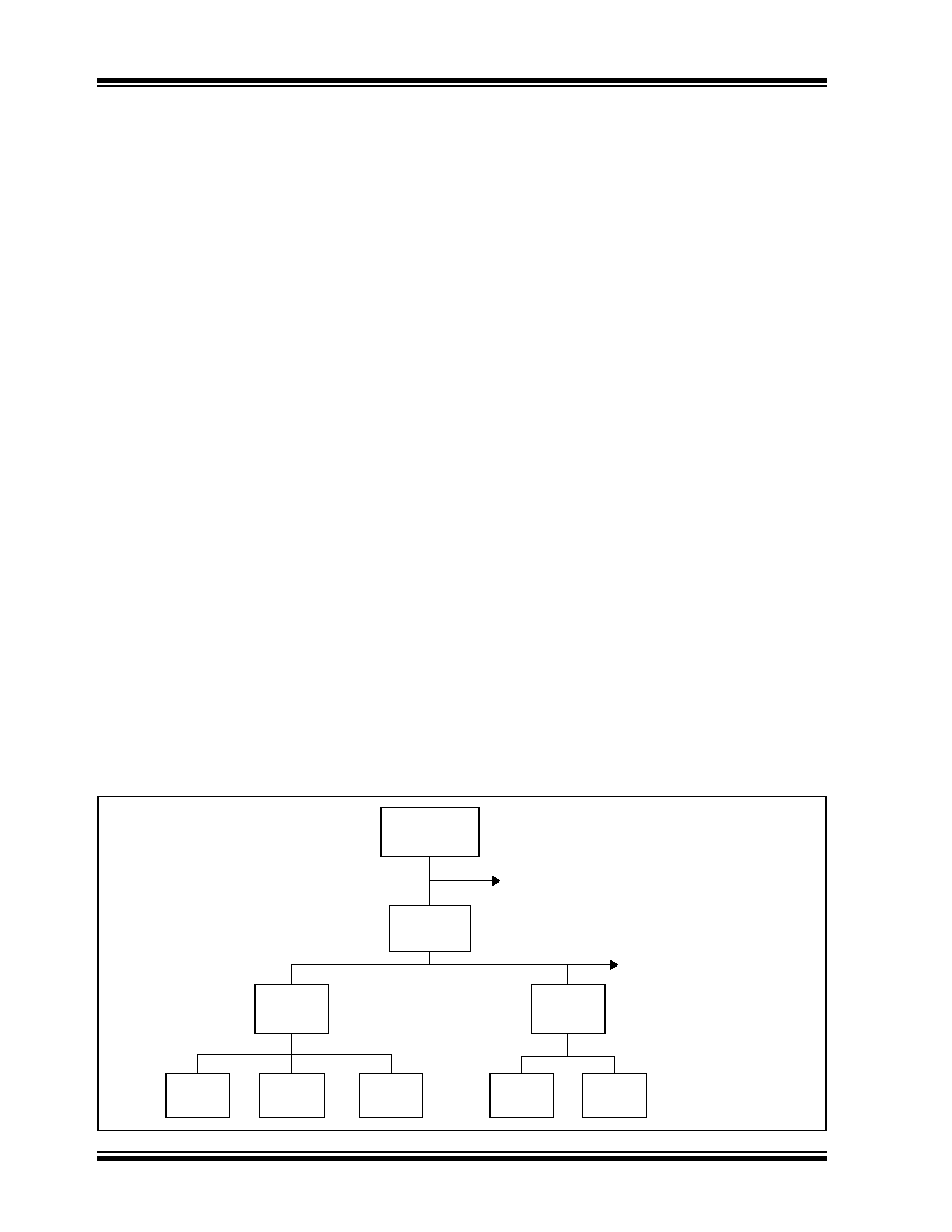
PIC18F2450/4450
DS39760A-page 150
Advance Information
� 2006 Microchip Technology Inc.
14.9
Overview of USB
This section presents some of the basic USB concepts
and useful information necessary to design a USB
device. Although much information is provided in this
section, there is a plethora of information provided
within the USB specifications and class specifications.
Thus, the reader is encouraged to refer to the USB
specifications for more information (www.usb.org). If
you are very familiar with the details of USB, then this
section serves as a basic, high-level refresher of USB.
14.9.1
LAYERED FRAMEWORK
USB device functionality is structured into a layered
framework graphically shown in Figure 14-13. Each
level is associated with a functional level within the
device. The highest layer, other than the device, is the
configuration. A device may have multiple configura-
tions. For example, a particular device may have
multiple power requirements based on Self-Power Only
or Bus Power Only modes.
For each configuration, there may be multiple
interfaces. Each interface could support a particular
mode of that configuration.
Below the interface is the endpoint(s). Data is directly
moved at this level. There can be as many as
16 bidirectional endpoints. Endpoint 0 is always a
control endpoint and by default, when the device is on
the bus, Endpoint 0 must be available to configure the
device.
14.9.2
FRAMES
Information communicated on the bus is grouped into
1 ms time slots, referred to as frames. Each frame can
contain many transactions to various devices and
endpoints. Figure 14-9 shows an example of a
transaction within a frame.
14.9.3
TRANSFERS
There are four transfer types defined in the USB
specification.
� Isochronous: This type provides a transfer
method for large amounts of data (up to
1023 bytes) with timely delivery ensured;
however, the data integrity is not ensured. This is
good for streaming applications where small data
loss is not critical, such as audio.
� Bulk: This type of transfer method allows for large
amounts of data to be transferred with ensured
data integrity; however, the delivery timeliness is
not ensured.
� Interrupt: This type of transfer provides for
ensured timely delivery for small blocks of data;
plus data integrity is ensured.
� Control: This type provides for device setup
control.
While full-speed devices support all transfer types,
low-speed devices are limited to interrupt and control
transfers only.
14.9.4
POWER
Power is available from the Universal Serial Bus. The
USB specification defines the bus power requirements.
Devices may either be self-powered or bus powered.
Self-powered devices draw power from an external
source, while bus powered devices use power supplied
from the bus.
FIGURE 14-13:
USB LAYERS
Device
Configuration
Interface
Endpoint
Interface
Endpoint
Endpoint
Endpoint
Endpoint
To other Configurations (if any)
To other Interfaces (if any)

PIC18F2450/4450
� 2006 Microchip Technology Inc.
Advance Information
DS39760A-page 151
The USB specification limits the power taken from the
bus. Each device is ensured 100 mA at approximately 5V
(one-unit load). Additional power may be requested, up
to a maximum of 500 mA. Note that power above a one-
unit load is a request and the host or hub is not obligated
to provide the extra current. Thus, a device capable of
consuming more than a one-unit load must be able to
maintain a low-power configuration of a one-unit load or
less, if necessary.
The USB specification also defines a Suspend mode.
In this situation, current must be limited to 500
A,
averaged over 1 second. A device must enter a
Suspend state after 3 ms of inactivity (i.e., no SOF
tokens for 3 ms). A device entering Suspend mode
must drop current consumption within 10 ms after
Suspend. Likewise, when signaling a wake-up, the
device must signal a wake-up within 10 ms of drawing
current above the Suspend limit.
14.9.5
ENUMERATION
When the device is initially attached to the bus, the host
enters an enumeration process in an attempt to identify
the device. Essentially, the host interrogates the device,
gathering information such as power consumption, data
rates and sizes, protocol and other descriptive
information; descriptors contain this information. A
typical enumeration process would be as follows:
1.
USB Reset: Reset the device. Thus, the device
is not configured and does not have an address
(address 0).
2.
Get Device Descriptor: The host requests a
small portion of the device descriptor.
3.
USB Reset: Reset the device again.
4.
Set Address: The host assigns an address to the
device.
5.
Get Device Descriptor: The host retrieves the
device descriptor, gathering info such as
manufacturer, type of device, maximum control
packet size.
6.
Get configuration descriptors.
7.
Get any other descriptors.
8.
Set a configuration.
The exact enumeration process depends on the host.
14.9.6
DESCRIPTORS
There are eight different standard descriptor types of
which five are most important for this device.
14.9.6.1
Device Descriptor
The device descriptor provides general information,
such as manufacturer, product number, serial number,
the class of the device and the number of configurations.
There is only one device descriptor.
14.9.6.2
Configuration Descriptor
The configuration descriptor provides information on
the power requirements of the device and how many
different interfaces are supported when in this
configuration. There may be more than one configura-
tion for a device (i.e., low-power and high-power
configurations).
14.9.6.3
Interface Descriptor
The interface descriptor details the number of
endpoints used in this interface, as well as the class of
the interface. There may be more than one interface for
a configuration.
14.9.6.4
Endpoint Descriptor
The endpoint descriptor identifies the transfer type
(Section 14.9.3 "Transfers") and direction, as well as
some other specifics for the endpoint. There may be
many endpoints in a device and endpoints may be
shared in different configurations.
14.9.6.5
String Descriptor
Many of the previous descriptors reference one or
more string descriptors. String descriptors provide
human readable information about the layer
(Section 14.9.1 "Layered Framework") they
describe. Often these strings show up in the host to
help the user identify the device. String descriptors are
generally optional to save memory and are encoded in
a unicode format.
14.9.7
BUS SPEED
Each USB device must indicate its bus presence and
speed to the host. This is accomplished through a
1.5 k
resistor which is connected to the bus at the
time of the attachment event.
Depending on the speed of the device, the resistor
either pulls up the D+ or D- line to 3.3V. For a low-
speed device, the pull-up resistor is connected to the
D- line. For a full-speed device, the pull-up resistor is
connected to the D+ line.
14.9.8
CLASS SPECIFICATIONS AND
DRIVERS
USB specifications include class specifications which
operating system vendors optionally support.
Examples of classes include Audio, Mass Storage,
Communications and Human Interface (HID). In most
cases, a driver is required at the host side to `talk' to the
USB device. In custom applications, a driver may need
to be developed. Fortunately, drivers are available for
most common host systems for the most common
classes of devices. Thus, these drivers can be reused.

PIC18F2450/4450
DS39760A-page 152
Advance Information
� 2006 Microchip Technology Inc.
NOTES:

PIC18F2450/4450
� 2006 Microchip Technology Inc.
Advance Information
DS39760A-page 153
15.0
ENHANCED UNIVERSAL
SYNCHRONOUS RECEIVER
TRANSMITTER (EUSART)
The Universal Synchronous Asynchronous Receiver
Transmitter (USART) module is one of the two serial
I/O modules. (USART is also known as a Serial
Communications Interface or SCI.) The USART can be
configured as a full-duplex asynchronous system that
can communicate with peripheral devices, such as
CRT terminals and personal computers. It can also be
configured as a half-duplex synchronous system that
can communicate with peripheral devices, such as A/D
or D/A integrated circuits, serial EEPROMs and so on.
The Enhanced Universal Synchronous Receiver
Transmitter (EUSART) module implements additional
features, including Automatic Baud Rate Detection
(ABD) and calibration, automatic wake-up on Sync
Break reception and 12-bit Break character transmit.
These features make it ideally suited for use in Local
Interconnect Network bus (LIN bus) systems.
The EUSART can be configured in the following
modes:
� Asynchronous (full-duplex) with:
- Auto-wake-up on character reception
- Auto-baud calibration
- 12-bit Break character transmission
� Synchronous � Master (half-duplex) with
selectable clock polarity
� Synchronous � Slave (half-duplex) with selectable
clock polarity
The pins of the Enhanced USART are multiplexed with
PORTC. In order to configure RC6/TX/CK and RC7/RX/
DT as an EUSART:
� bit SPEN (RCSTA<7>) must be set (= 1)
� bit TRISC<7> must be set (= 1)
� bit TRISC<6> must be cleared (= 0) for
Asynchronous and Synchronous Master modes
or set (= 1) for Synchronous Slave mode
The operation of the Enhanced USART module is
controlled through three registers:
� Transmit Status and Control (TXSTA)
� Receive Status and Control (RCSTA)
� Baud Rate Control (BAUDCON)
These are detailed on the following pages in
Register 15-1, Register 15-2 and Register 15-3,
respectively.
Note:
The EUSART control will automatically
reconfigure the pin from input to output as
needed.

PIC18F2450/4450
DS39760A-page 154
Advance Information
� 2006 Microchip Technology Inc.
REGISTER 15-1:
TXSTA: TRANSMIT STATUS AND CONTROL REGISTER
R/W-0
R/W-0
R/W-0
R/W-0
R/W-0
R/W-0
R-1
R/W-0
CSRC
TX9
TXEN
(1)
SYNC
SENDB
BRGH
TRMT
TX9D
bit 7
bit 0
Legend:
R = Readable bit
W = Writable bit
U = Unimplemented bit, read as `0'
-n = Value at POR
`1' = Bit is set
`0' = Bit is cleared
x = Bit is unknown
bit 7
CSRC: Clock Source Select bit
Asynchronous mode:
Don't care.
Synchronous mode:
1
= Master mode (clock generated internally from BRG)
0
= Slave mode (clock from external source)
bit 6
TX9: 9-Bit Transmit Enable bit
1
= Selects 9-bit transmission
0
= Selects 8-bit transmission
bit 5
TXEN: Transmit Enable bit
(1)
1
= Transmit enabled
0
= Transmit disabled
bit 4
SYNC: EUSART Mode Select bit
1
= Synchronous mode
0
= Asynchronous mode
bit 3
SENDB: Send Break Character bit
Asynchronous mode:
1
= Send Sync Break on next transmission (cleared by hardware upon completion)
0
= Sync Break transmission completed
Synchronous mode:
Don't care.
bit 2
BRGH: High Baud Rate Select bit
Asynchronous mode:
1
= High speed
0
= Low speed
Synchronous mode:
Unused in this mode.
bit 1
TRMT: Transmit Shift Register Status bit
1
= TSR empty
0
= TSR full
bit 0
TX9D: 9th bit of Transmit Data
Can be address/data bit or a parity bit.
Note 1:
SREN/CREN overrides TXEN in Sync mode with the exception that SREN has no effect in Synchronous
Slave mode.

PIC18F2450/4450
� 2006 Microchip Technology Inc.
Advance Information
DS39760A-page 155
REGISTER 15-2:
RCSTA: RECEIVE STATUS AND CONTROL REGISTER
R/W-0
R/W-0
R/W-0
R/W-0
R/W-0
R-0
R-0
R-x
SPEN
RX9
SREN
CREN
ADDEN
FERR
OERR
RX9D
bit 7
bit 0
Legend:
R = Readable bit
W = Writable bit
U = Unimplemented bit, read as `0'
-n = Value at POR
`1' = Bit is set
`0' = Bit is cleared
x = Bit is unknown
bit 7
SPEN: Serial Port Enable bit
1
= Serial port enabled (configures RX/DT and TX/CK pins as serial port pins)
0
= Serial port disabled (held in Reset)
bit 6
RX9: 9-Bit Receive Enable bit
1
= Selects 9-bit reception
0
= Selects 8-bit reception
bit 5
SREN: Single Receive Enable bit
Asynchronous mode:
Don't care.
Synchronous mode � Master:
1
= Enables single receive
0
= Disables single receive
This bit is cleared after reception is complete.
Synchronous mode � Slave:
Don't care.
bit 4
CREN: Continuous Receive Enable bit
Asynchronous mode:
1
= Enables receiver
0
= Disables receiver
Synchronous mode:
1
= Enables continuous receive until enable bit CREN is cleared (CREN overrides SREN)
0
= Disables continuous receive
bit 3
ADDEN: Address Detect Enable bit
Asynchronous mode 9-bit (RX9 = 1):
1
= Enables address detection, enables interrupt and loads the receive buffer when RSR<8> is set
0
= Disables address detection, all bytes are received and ninth bit can be used as parity bit
Asynchronous mode 9-bit (RX9 = 0):
Don't care.
bit 2
FERR: Framing Error bit
1
= Framing error (can be updated by reading RCREG register and receiving next valid byte)
0
= No framing error
bit 1
OERR: Overrun Error bit
1
= Overrun error (can be cleared by clearing bit CREN)
0
= No overrun error
bit 0
RX9D: 9th bit of Received Data
This can be address/data bit or a parity bit and must be calculated by user firmware.

PIC18F2450/4450
DS39760A-page 156
Advance Information
� 2006 Microchip Technology Inc.
REGISTER 15-3:
BAUDCON: BAUD RATE CONTROL REGISTER
R/W-0
R-1
U-0
R/W-0
R/W-0
U-0
R/W-0
R/W-0
ABDOVF
RCIDL
--
SCKP
BRG16
--
WUE
ABDEN
bit 7
bit 0
Legend:
R = Readable bit
W = Writable bit
U = Unimplemented bit, read as `0'
-n = Value at POR
`1' = Bit is set
`0' = Bit is cleared
x = Bit is unknown
bit 7
ABDOVF: Auto-Baud Acquisition Rollover Status bit
1
= A BRG rollover has occurred during Auto-Baud Rate Detect mode (must be cleared in software)
0
= No BRG rollover has occurred
bit 6
RCIDL: Receive Operation Idle Status bit
1
= Receive operation is Idle
0
= Receive operation is active
bit 5
Unimplemented: Read as `0'
bit 4
SCKP: Synchronous Clock Polarity Select bit
Asynchronous mode:
Unused in this mode.
Synchronous mode:
1
= Idle state for clock (CK) is a high level
0
= Idle state for clock (CK) is a low level
bit 3
BRG16: 16-Bit Baud Rate Register Enable bit
1
= 16-bit Baud Rate Generator � SPBRGH and SPBRG
0
= 8-bit Baud Rate Generator � SPBRG only (Compatible mode), SPBRGH value ignored
bit 2
Unimplemented: Read as `0'
bit 1
WUE: Wake-up Enable bit
Asynchronous mode:
1
= EUSART will continue to sample the RX pin � interrupt generated on falling edge; bit cleared in
hardware on following rising edge
0
= RX pin not monitored or rising edge detected
Synchronous mode:
Unused in this mode.
bit 0
ABDEN: Auto-Baud Detect Enable bit
Asynchronous mode:
1
= Enable baud rate measurement on the next character. Requires reception of a Sync field (55h);
cleared in hardware upon completion.
0
= Baud rate measurement disabled or completed
Synchronous mode:
Unused in this mode.
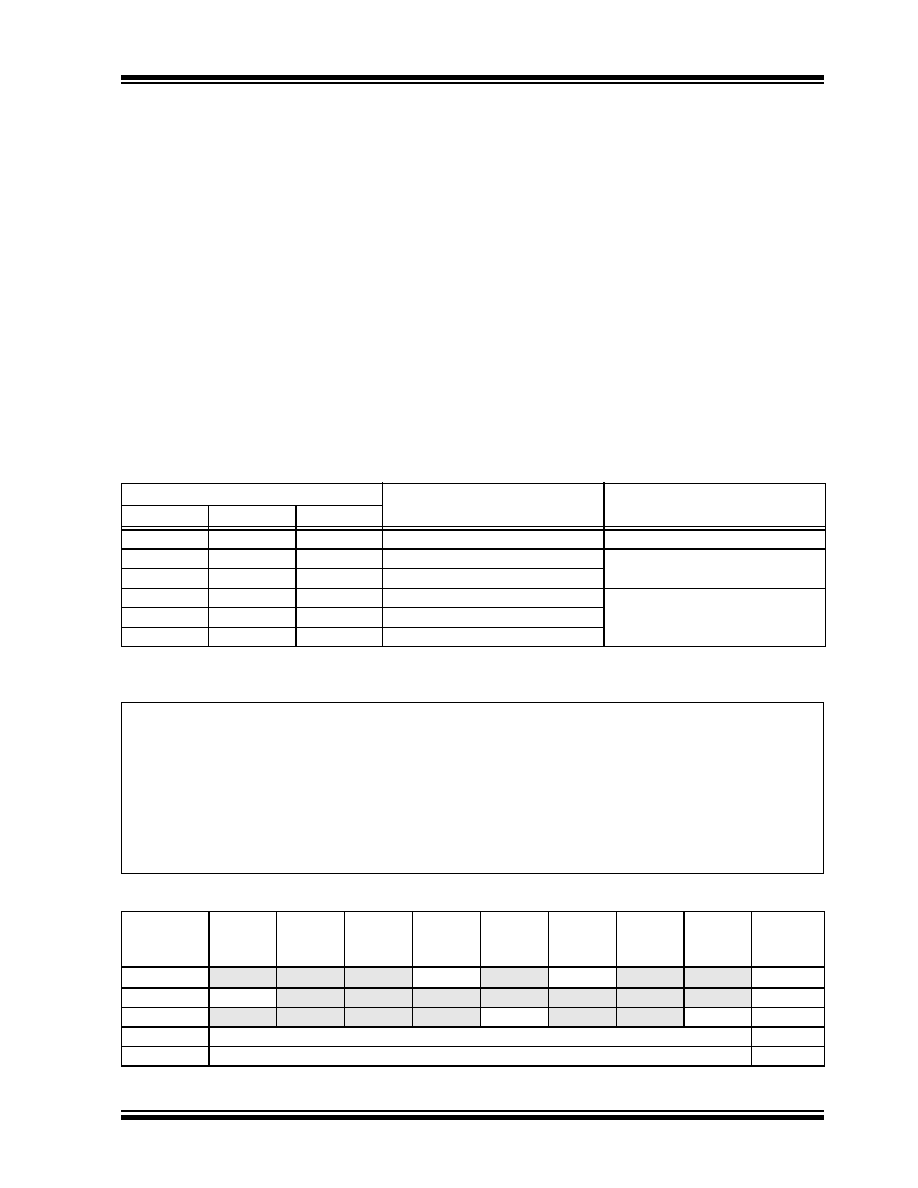
PIC18F2450/4450
� 2006 Microchip Technology Inc.
Advance Information
DS39760A-page 157
15.1
Baud Rate Generator (BRG)
The BRG is a dedicated 8-bit or 16-bit generator that
supports both the Asynchronous and Synchronous
modes of the EUSART. By default, the BRG operates
in 8-bit mode. Setting the BRG16 bit (BAUDCON<3>)
selects 16-bit mode.
The SPBRGH:SPBRG register pair controls the period
of a free-running timer. In Asynchronous mode, bits
BRGH (TXSTA<2>) and BRG16 (BAUDCON<3>) also
control the baud rate. In Synchronous mode, BRGH is
ignored. Table 15-1 shows the formula for computation
of the baud rate for different EUSART modes which
only apply in Master mode (internally generated clock).
Given the desired baud rate and F
OSC
, the nearest
integer value for the SPBRGH:SPBRG registers can be
calculated using the formulas in Table 15-1. From this,
the error in baud rate can be determined. An example
calculation is shown in Example 15-1. Typical baud rates
and error values for the various Asynchronous modes
are shown in Table 15-2. It may be advantageous to use
the high baud rate (BRGH = 1) or the 16-bit BRG to
reduce the baud rate error, or achieve a slow baud rate
for a fast oscillator frequency.
Writing a new value to the SPBRGH:SPBRG registers
causes the BRG timer to be reset (or cleared). This
ensures the BRG does not wait for a timer overflow
before outputting the new baud rate.
15.1.1
OPERATION IN POWER-MANAGED
MODES
The device clock is used to generate the desired baud
rate. When one of the power-managed modes is
entered, the new clock source may be operating at a
different frequency. This may require an adjustment to
the value in the SPBRG register pair.
15.1.2
SAMPLING
The data on the RX pin is sampled three times by a
majority detect circuit to determine if a high or a low
level is present at the RX pin.
TABLE 15-1:
BAUD RATE FORMULAS
EXAMPLE 15-1:
CALCULATING BAUD RATE ERROR
TABLE 15-2:
REGISTERS ASSOCIATED WITH BAUD RATE GENERATOR
Configuration Bits
BRG/EUSART Mode
Baud Rate Formula
SYNC
BRG16
BRGH
0
0
0
8-bit/Asynchronous
F
OSC
/[64 (n + 1)]
0
0
1
8-bit/Asynchronous
F
OSC
/[16 (n + 1)]
0
1
0
16-bit/Asynchronous
0
1
1
16-bit/Asynchronous
F
OSC
/[4 (n + 1)]
1
0
x
8-bit/Synchronous
1
1
x
16-bit/Synchronous
Legend: x = Don't care, n = value of SPBRGH:SPBRG register pair
Name
Bit 7
Bit 6
Bit 5
Bit 4
Bit 3
Bit 2
Bit 1
Bit 0
Reset
Values
on page
TXSTA
CSRC
TX9
TXEN
SYNC
SENDB
BRGH
TRMT
TX9D
51
RCSTA
SPEN
RX9
SREN
CREN
ADDEN
FERR
OERR
RX9D
51
BAUDCON
ABDOVF
RCIDL
--
SCKP
BRG16
--
WUE
ABDEN
51
SPBRGH
EUSART Baud Rate Generator Register High Byte
50
SPBRG
EUSART Baud Rate Generator Register Low Byte
50
Legend: -- = unimplemented, read as `0'. Shaded cells are not used by the BRG.
For a device with F
OSC
of 16 MHz, desired baud rate of 9600, Asynchronous mode, 8-bit BRG:
Desired Baud Rate
= F
OSC
/(64 ([SPBRGH:SPBRG] + 1)
Solving for SPBRGH:SPBRG:
X
=
((F
OSC
/Desired Baud Rate)/64) � 1
=
((16000000/9600)/64) � 1
=
[25.042] = 25
Calculated Baud Rate
=
16000000/(64 (25 + 1))
=
9615
Error
=
(Calculated Baud Rate � Desired Baud Rate)/Desired Baud Rate
=
(9615 � 9600)/9600 = 0.16%

PIC18F2450/4450
DS39760A-page 158
Advance Information
� 2006 Microchip Technology Inc.
TABLE 15-3:
BAUD RATES FOR ASYNCHRONOUS MODES
BAUD
RATE
(K)
SYNC = 0, BRGH = 0, BRG16 = 0
F
OSC
= 40.000 MHz
F
OSC
= 20.000 MHz
F
OSC
= 10.000 MHz
F
OSC
= 8.000 MHz
Actual
Rate
(K)
%
Error
SPBRG
value
(decimal)
Actual
Rate
(K)
%
Error
SPBRG
value
(decimal)
Actual
Rate
(K)
%
Error
SPBRG
value
(decimal)
Actual
Rate
(K)
%
Error
SPBRG
value
(decimal)
0.3
--
--
--
--
--
--
--
--
--
--
--
--
1.2
--
--
--
1.221
1.73
255
1.202
0.16
129
1201
-0.16
103
2.4
2.441
1.73
255
2.404
0.16
129
2.404
0.16
64
2403
-0.16
51
9.6
9.615
0.16
64
9.766
1.73
31
9.766
1.73
15
9615
-0.16
12
19.2
19.531
1.73
31
19.531
1.73
15
19.531
1.73
7
--
--
--
57.6
56.818
-1.36
10
62.500
8.51
4
52.083
-9.58
2
--
--
--
115.2
125.000
8.51
4
104.167
-9.58
2
78.125
-32.18
1
--
--
--
BAUD
RATE
(K)
SYNC = 0, BRGH = 0, BRG16 = 0
F
OSC
= 4.000 MHz
F
OSC
= 2.000 MHz
F
OSC
= 1.000 MHz
Actual
Rate
(K)
%
Error
SPBRG
value
(decimal)
Actual
Rate
(K)
%
Error
SPBRG
value
(decimal)
Actual
Rate
(K)
%
Error
SPBRG
value
(decimal)
0.3
0.300
0.16
207
300
-0.16
103
300
-0.16
51
1.2
1.202
0.16
51
1201
-0.16
25
1201
-0.16
12
2.4
2.404
0.16
25
2403
-0.16
12
--
--
--
9.6
8.929
-6.99
6
--
--
--
--
--
--
19.2
20.833
8.51
2
--
--
--
--
--
--
57.6
62.500
8.51
0
--
--
--
--
--
--
115.2
62.500
-45.75
0
--
--
--
--
--
--
BAUD
RATE
(K)
SYNC = 0, BRGH = 1, BRG16 = 0
F
OSC
= 40.000 MHz
F
OSC
= 20.000 MHz
F
OSC
= 10.000 MHz
F
OSC
= 8.000 MHz
Actual
Rate
(K)
%
Error
SPBRG
value
(decimal)
Actual
Rate
(K)
%
Error
SPBRG
value
(decimal)
Actual
Rate
(K)
%
Error
SPBRG
value
(decimal)
Actual
Rate
(K)
%
Error
SPBRG
value
(decimal)
0.3
--
--
--
--
--
--
--
--
--
--
--
--
1.2
--
--
--
--
--
--
--
--
--
--
--
--
2.4
--
--
--
--
--
--
2.441
1.73
255
2403
-0.16
207
9.6
9.766
1.73
255
9.615
0.16
129
9.615
0.16
64
9615
-0.16
51
19.2
19.231
0.16
129
19.231
0.16
64
19.531
1.73
31
19230
-0.16
25
57.6
58.140
0.94
42
56.818
-1.36
21
56.818
-1.36
10
55555
3.55
8
115.2
113.636
-1.36
21
113.636
-1.36
10
125.000
8.51
4
--
--
--
BAUD
RATE
(K)
SYNC = 0, BRGH = 1, BRG16 = 0
F
OSC
= 4.000 MHz
F
OSC
= 2.000 MHz
F
OSC
= 1.000 MHz
Actual
Rate
(K)
%
Error
SPBRG
value
(decimal)
Actual
Rate
(K)
%
Error
SPBRG
value
(decimal)
Actual
Rate
(K)
%
Error
SPBRG
value
(decimal)
0.3
--
--
--
--
--
--
300
-0.16
207
1.2
1.202
0.16
207
1201
-0.16
103
1201
-0.16
51
2.4
2.404
0.16
103
2403
-0.16
51
2403
-0.16
25
9.6
9.615
0.16
25
9615
-0.16
12
--
--
--
19.2
19.231
0.16
12
--
--
--
--
--
--
57.6
62.500
8.51
3
--
--
--
--
--
--
115.2
125.000
8.51
1
--
--
--
--
--
--

PIC18F2450/4450
� 2006 Microchip Technology Inc.
Advance Information
DS39760A-page 159
BAUD
RATE
(K)
SYNC = 0, BRGH = 0, BRG16 = 1
F
OSC
= 40.000 MHz
F
OSC
= 20.000 MHz
F
OSC
= 10.000 MHz
F
OSC
= 8.000 MHz
Actual
Rate
(K)
%
Error
SPBRG
value
(decimal)
Actual
Rate
(K)
%
Error
SPBRG
value
(decimal)
Actual
Rate
(K)
%
Error
SPBRG
value
(decimal)
Actual
Rate
(K)
%
Error
SPBRG
value
(decimal)
0.3
0.300
0.00
8332
0.300
0.02
4165
0.300
0.02
2082
300
-0.04
1665
1.2
1.200
0.02
2082
1.200
-0.03
1041
1.200
-0.03
520
1201
-0.16
415
2.4
2.402
0.06
1040
2.399
-0.03
520
2.404
0.16
259
2403
-0.16
207
9.6
9.615
0.16
259
9.615
0.16
129
9.615
0.16
64
9615
-0.16
51
19.2
19.231
0.16
129
19.231
0.16
64
19.531
1.73
31
19230
-0.16
25
57.6
58.140
0.94
42
56.818
-1.36
21
56.818
-1.36
10
55555
3.55
8
115.2
113.636
-1.36
21
113.636
-1.36
10
125.000
8.51
4
--
--
--
BAUD
RATE
(K)
SYNC = 0, BRGH = 0, BRG16 = 1
F
OSC
= 4.000 MHz
F
OSC
= 2.000 MHz
F
OSC
= 1.000 MHz
Actual
Rate
(K)
%
Error
SPBRG
value
(decimal)
Actual
Rate
(K)
%
Error
SPBRG
value
(decimal)
Actual
Rate
(K)
%
Error
SPBRG
value
(decimal)
0.3
0.300
0.04
832
300
-0.16
415
300
-0.16
207
1.2
1.202
0.16
207
1201
-0.16
103
1201
-0.16
51
2.4
2.404
0.16
103
2403
-0.16
51
2403
-0.16
25
9.6
9.615
0.16
25
9615
-0.16
12
--
--
--
19.2
19.231
0.16
12
--
--
--
--
--
--
57.6
62.500
8.51
3
--
--
--
--
--
--
115.2
125.000
8.51
1
--
--
--
--
--
--
BAUD
RATE
(K)
SYNC = 0, BRGH = 1, BRG16 = 1 or SYNC = 1, BRG16 = 1
F
OSC
= 40.000 MHz
F
OSC
= 20.000 MHz
F
OSC
= 10.000 MHz
F
OSC
= 8.000 MHz
Actual
Rate
(K)
%
Error
SPBRG
value
(decimal)
Actual
Rate
(K)
%
Error
SPBRG
value
(decimal)
Actual
Rate
(K)
%
Error
SPBRG
value
(decimal)
Actual
Rate
(K)
%
Error
SPBRG
value
(decimal)
0.3
0.300
0.00
33332
0.300
0.00
16665
0.300
0.00
8332
300
-0.01
6665
1.2
1.200
0.00
8332
1.200
0.02
4165
1.200
0.02
2082
1200
-0.04
1665
2.4
2.400
0.02
4165
2.400
0.02
2082
2.402
0.06
1040
2400
-0.04
832
9.6
9.606
0.06
1040
9.596
-0.03
520
9.615
0.16
259
9615
-0.16
207
19.2
19.193
-0.03
520
19.231
0.16
259
19.231
0.16
129
19230
-0.16
103
57.6
57.803
0.35
172
57.471
-0.22
86
58.140
0.94
42
57142
0.79
34
115.2
114.943
-0.22
86
116.279
0.94
42
113.636
-1.36
21
117647
-2.12
16
BAUD
RATE
(K)
SYNC = 0, BRGH = 1, BRG16 = 1 or SYNC = 1, BRG16 = 1
F
OSC
= 4.000 MHz
F
OSC
= 2.000 MHz
F
OSC
= 1.000 MHz
Actual
Rate
(K)
%
Error
SPBRG
value
(decimal)
Actual
Rate
(K)
%
Error
SPBRG
value
(decimal)
Actual
Rate
(K)
%
Error
SPBRG
value
(decimal)
0.3
0.300
0.01
3332
300
-0.04
1665
300
-0.04
832
1.2
1.200
0.04
832
1201
-0.16
415
1201
-0.16
207
2.4
2.404
0.16
415
2403
-0.16
207
2403
-0.16
103
9.6
9.615
0.16
103
9615
-0.16
51
9615
-0.16
25
19.2
19.231
0.16
51
19230
-0.16
25
19230
-0.16
12
57.6
58.824
2.12
16
55555
3.55
8
--
--
--
115.2
111.111
-3.55
8
--
--
--
--
--
--
TABLE 15-3:
BAUD RATES FOR ASYNCHRONOUS MODES (CONTINUED)

PIC18F2450/4450
DS39760A-page 160
Advance Information
� 2006 Microchip Technology Inc.
15.1.3
AUTO-BAUD RATE DETECT
The Enhanced USART module supports the automatic
detection and calibration of baud rate. This feature is
active only in Asynchronous mode and while the WUE
bit is clear.
The automatic baud rate measurement sequence
(Figure 15-1) begins whenever a Start bit is received
and the ABDEN bit is set. The calculation is self-aver-
aging.
In the Auto-Baud Rate Detect (ABD) mode, the clock to
the BRG is reversed. Rather than the BRG clocking the
incoming RX signal, the RX signal is timing the BRG. In
ABD mode, the internal Baud Rate Generator is used
as a counter to time the bit period of the incoming serial
byte stream.
Once the ABDEN bit is set, the state machine will clear
the BRG and look for a Start bit. The Auto-Baud Rate
Detection must receive a byte with the value 55h
(ASCII "U", which is also the LIN bus Sync character)
in order to calculate the proper bit rate. The measure-
ment is taken over both a low and a high bit time in
order to minimize any effects caused by asymmetry of
the incoming signal. After a Start bit, the SPBRG
begins counting up, using the preselected clock source
on the first rising edge of RX. After eight bits on the RX
pin, or the fifth rising edge, an accumulated value
totalling the proper BRG period is left in the
SPBRGH:SPBRG register pair. Once the 5th edge is
seen (this should correspond to the Stop bit), the
ABDEN bit is automatically cleared.
If a rollover of the BRG occurs (an overflow from FFFFh
to 0000h), the event is trapped by the ABDOVF status
bit (BAUDCON<7>). It is set in hardware by BRG roll-
overs and can be set or cleared by the user in software.
ABD mode remains active after rollover events and the
ABDEN bit remains set (Figure 15-2).
While calibrating the baud rate period, the BRG
registers are clocked at 1/8th the preconfigured clock
rate. Note that the BRG clock will be configured by the
BRG16 and BRGH bits. Independent of the BRG16 bit
setting, both the SPBRG and SPBRGH will be used as
a 16-bit counter. This allows the user to verify that no
carry occurred for 8-bit modes by checking for 00h in
the SPBRGH register. Refer to Table 15-4 for counter
clock rates to the BRG.
While the ABD sequence takes place, the EUSART
state machine is held in Idle. The RCIF interrupt is set
once the fifth rising edge on RX is detected. The value
in the RCREG needs to be read to clear the RCIF
interrupt. The contents of RCREG should be discarded.
TABLE 15-4:
BRG COUNTER
CLOCK RATES
15.1.3.1
ABD and EUSART Transmission
Since the BRG clock is reversed during ABD
acquisition, the EUSART transmitter cannot be used
during ABD. This means that whenever the ABDEN bit
is set, TXREG cannot be written to. Users should also
ensure that ABDEN does not become set during a
transmit sequence. Failing to do this may result in
unpredictable EUSART operation.
Note 1: If the WUE bit is set with the ABDEN bit,
Auto-Baud Rate Detection will occur on
the byte
following the Break character.
2: It is up to the user to determine that the
incoming character baud rate is within the
range of the selected BRG clock source.
Some combinations of oscillator fre-
quency and EUSART baud rates are not
possible due to bit error rates. Overall
system timing and communication baud
rates must be taken into consideration
when using the Auto-Baud Rate
Detection feature.
BRG16
BRGH
BRG Counter Clock
0
0
F
OSC
/512
0
1
F
OSC
/128
1
0
F
OSC
/128
1
1
F
OSC
/32
Note:
During the ABD sequence, SPBRG and
SPBRGH are both used as a 16-bit counter,
independent of the BRG16 setting.
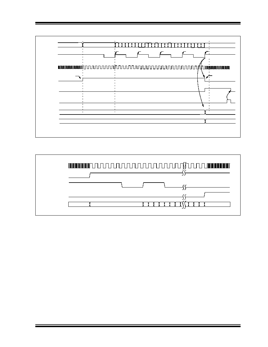
PIC18F2450/4450
� 2006 Microchip Technology Inc.
Advance Information
DS39760A-page 161
FIGURE 15-1:
AUTOMATIC BAUD RATE CALCULATION
FIGURE 15-2:
BRG OVERFLOW SEQUENCE
BRG Value
RX pin
ABDEN bit
RCIF bit
bit 0
bit 1
(Interrupt)
Read
RCREG
BRG Clock
Start
Auto-Cleared
Set by User
XXXXh
0000h
Edge #1
bit 2
bit 3
Edge #2
bit 4
bit 5
Edge #3
bit 6
bit 7
Edge #4
Edge #5
001Ch
Note: The ABD sequence requires the EUSART module to be configured in Asynchronous mode and WUE = 0.
SPBRG
XXXXh
1Ch
SPBRGH
XXXXh
00h
Stop bit
Start
bit 0
XXXXh
0000h
0000h
FFFFh
BRG Clock
ABDEN bit
RX pin
ABDOVF bit
BRG Value
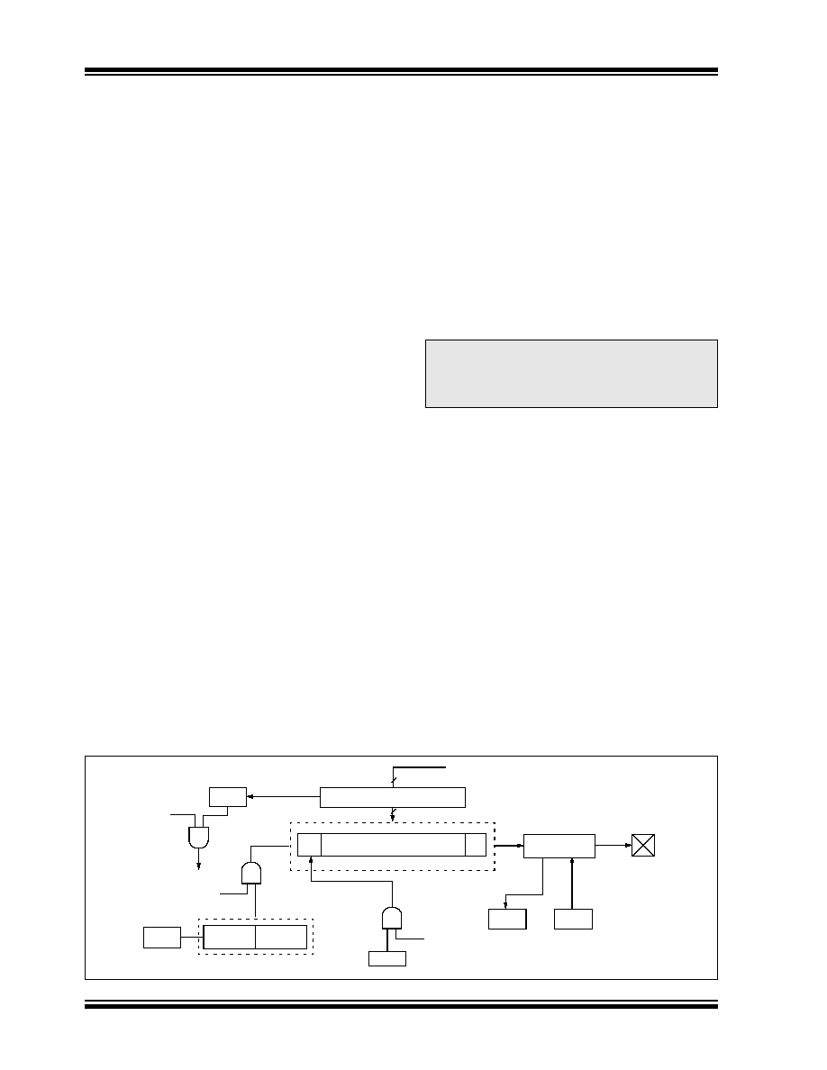
PIC18F2450/4450
DS39760A-page 162
Advance Information
� 2006 Microchip Technology Inc.
15.2
EUSART Asynchronous Mode
The Asynchronous mode of operation is selected by
clearing the SYNC bit (TXSTA<4>). In this mode, the
EUSART uses the standard Non-Return-to-Zero (NRZ)
format (one Start bit, eight or nine data bits and one
Stop bit). The most common data format is eight bits.
An on-chip dedicated 8-bit/16-bit Baud Rate Generator
can be used to derive standard baud rate frequencies
from the oscillator.
The EUSART transmits and receives the LSb first. The
EUSART's transmitter and receiver are functionally
independent but use the same data format and baud
rate. The Baud Rate Generator produces a clock, either
x16 or x64 of the bit shift rate depending on the BRGH
and BRG16 bits (TXSTA<2> and BAUDCON<3>). Parity
is not supported by the hardware but can be
implemented in software and stored as the ninth data bit.
When operating in Asynchronous mode, the EUSART
module consists of the following important elements:
� Baud Rate Generator
� Sampling Circuit
� Asynchronous Transmitter
� Asynchronous Receiver
� Auto-Wake-up on Sync Break Character
� 12-Bit Break Character Transmit
� Auto-Baud Rate Detection
15.2.1
EUSART ASYNCHRONOUS
TRANSMITTER
The EUSART transmitter block diagram is shown in
Figure 15-3. The heart of the transmitter is the Transmit
(Serial) Shift Register (TSR). The Shift register obtains
its data from the Read/Write Transmit Buffer register,
TXREG. The TXREG register is loaded with data in
software. The TSR register is not loaded until the Stop
bit has been transmitted from the previous load. As
soon as the Stop bit is transmitted, the TSR is loaded
with new data from the TXREG register (if available).
Once the TXREG register transfers the data to the TSR
register (occurs in one T
CY
), the TXREG register is empty
and the TXIF flag bit (PIR1<4>) is set. This interrupt can
be enabled or disabled by setting or clearing the interrupt
enable bit, TXIE (PIE1<4>). TXIF will be set regardless of
the state of TXIE; it cannot be cleared in software. TXIF
is also not cleared immediately upon loading TXREG but
becomes valid in the second instruction cycle following
the load instruction. Polling TXIF immediately following a
load of TXREG will return invalid results.
While TXIF indicates the status of the TXREG register,
another bit, TRMT (TXSTA<1>), shows the status of
the TSR register. TRMT is a read-only bit which is set
when the TSR register is empty. No interrupt logic is
tied to this bit so the user has to poll this bit in order to
determine if the TSR register is empty.
To set up an Asynchronous Transmission:
1.
Initialize the SPBRGH:SPBRG registers for the
appropriate baud rate. Set or clear the BRGH
and BRG16 bits, as required, to achieve the
desired baud rate.
2.
Enable the asynchronous serial port by clearing
bit SYNC and setting bit SPEN.
3.
If interrupts are desired, set enable bit TXIE.
4.
If 9-bit transmission is desired, set transmit bit
TX9. Can be used as address/data bit.
5.
Enable the transmission by setting bit TXEN
which will also set bit TXIF.
6.
If 9-bit transmission is selected, the ninth bit
should be loaded in bit TX9D.
7.
Load data to the TXREG register (starts
transmission).
8.
If using interrupts, ensure that the GIE and PEIE
bits in the INTCON register (INTCON<7:6>) are
set.
FIGURE 15-3:
EUSART TRANSMIT BLOCK DIAGRAM
Note 1: The TSR register is not mapped in data
memory so it is not available to the user.
2: Flag bit TXIF is set when enable bit TXEN
is set.
TXIF
TXIE
Interrupt
TXEN
Baud Rate CLK
SPBRG
Baud Rate Generator
MSb
LSb
Data Bus
TXREG Register
TSR Register
(8)
0
TX9
TRMT
SPEN
TX pin
Pin Buffer
and Control
8
� � �
SPBRGH
BRG16
TX9D
PIC18F2450/4450
� 2006 Microchip Technology Inc.
Advance Information
DS39760A-page 163
FIGURE 15-4:
ASYNCHRONOUS TRANSMISSION
FIGURE 15-5:
ASYNCHRONOUS TRANSMISSION (BACK TO BACK)
TABLE 15-5:
REGISTERS ASSOCIATED WITH ASYNCHRONOUS TRANSMISSION
Word 1
Word 1
Transmit Shift Reg
Start bit
bit 0
bit 1
bit 7/8
Write to TXREG
BRG Output
(Shift Clock)
TX
TXIF bit
(Transmit Buffer
Reg. Empty Flag)
TRMT bit
(Transmit Shift
Reg. Empty Flag)
1 T
CY
(pin)
Word 1
Stop bit
Transmit Shift Reg.
Write to TXREG
BRG Output
(Shift Clock)
TX
TXIF bit
(Interrupt Reg. Flag)
TRMT bit
(Transmit Shift
Reg. Empty Flag)
Word 1
Word 2
Word 1
Word 2
Stop bit
Start bit
Transmit Shift Reg.
Word 1
Word 2
bit 0
bit 1
bit 7/8
bit 0
Note:
This timing diagram shows two consecutive transmissions.
1 T
CY
1 T
CY
(pin)
Start bit
Name
Bit 7
Bit 6
Bit 5
Bit 4
Bit 3
Bit 2
Bit 1
Bit 0
Reset
Values
on page
INTCON
GIE/GIEH PEIE/GIEL
TMR0IE
INT0IE
RBIE
TMR0IF
INT0IF
RBIF
49
PIR1
--
ADIF
RCIF
TXIF
--
CCP1IF
TMR2IF
TMR1IF
51
PIE1
--
ADIE
RCIE
TXIE
--
CCP1IE
TMR2IE
TMR1IE
51
IPR1
--
ADIP
RCIP
TXIP
--
CCP1IP
TMR2IP
TMR1IP
51
RCSTA
SPEN
RX9
SREN
CREN
ADDEN
FERR
OERR
RX9D
51
TXREG
EUSART Transmit Register
50
TXSTA
CSRC
TX9
TXEN
SYNC
SENDB
BRGH
TRMT
TX9D
51
BAUDCON
ABDOVF
RCIDL
--
SCKP
BRG16
--
WUE
ABDEN
51
SPBRGH
EUSART Baud Rate Generator Register High Byte
50
SPBRG
EUSART Baud Rate Generator Register Low Byte
50
Legend: -- = unimplemented locations read as `0'. Shaded cells are not used for asynchronous transmission.
PIC18F2450/4450
DS39760A-page 164
Advance Information
� 2006 Microchip Technology Inc.
15.2.2
EUSART ASYNCHRONOUS
RECEIVER
The receiver block diagram is shown in Figure 15-6.
The data is received on the RX pin and drives the data
recovery block. The data recovery block is actually a
high-speed shifter operating at x16 times the baud rate,
whereas the main receive serial shifter operates at the
bit rate or at F
OSC
. This mode would typically be used
in RS-232 systems.
To set up an Asynchronous Reception:
1.
Initialize the SPBRGH:SPBRG registers for the
appropriate baud rate. Set or clear the BRGH
and BRG16 bits, as required, to achieve the
desired baud rate.
2.
Enable the asynchronous serial port by clearing
bit SYNC and setting bit SPEN.
3.
If interrupts are desired, set enable bit RCIE.
4.
If 9-bit reception is desired, set bit RX9.
5.
Enable the reception by setting bit CREN.
6.
Flag bit RCIF will be set when reception is
complete and an interrupt will be generated if
enable bit RCIE was set.
7.
Read the RCSTA register to get the ninth bit (if
enabled) and determine if any error occurred
during reception.
8.
Read the 8-bit received data by reading the
RCREG register.
9.
If any error occurred, clear the error by clearing
enable bit CREN.
10. If using interrupts, ensure that the GIE and PEIE
bits in the INTCON register (INTCON<7:6>) are
set.
15.2.3
SETTING UP 9-BIT MODE WITH
ADDRESS DETECT
This mode would typically be used in RS-485 systems.
To set up an Asynchronous Reception with Address
Detect Enable:
1.
Initialize the SPBRGH:SPBRG registers for the
appropriate baud rate. Set or clear the BRGH
and BRG16 bits, as required, to achieve the
desired baud rate.
2.
Enable the asynchronous serial port by clearing
the SYNC bit and setting the SPEN bit.
3.
If interrupts are required, set the RCEN bit and
select the desired priority level with the RCIP bit.
4.
Set the RX9 bit to enable 9-bit reception.
5.
Set the ADDEN bit to enable address detect.
6.
Enable reception by setting the CREN bit.
7.
The RCIF bit will be set when reception is
complete. The interrupt will be Acknowledged if
the RCIE and GIE bits are set.
8.
Read the RCSTA register to determine if any
error occurred during reception, as well as read
bit 9 of data (if applicable).
9.
Read RCREG to determine if the device is being
addressed.
10. If any error occurred, clear the CREN bit.
11. If the device has been addressed, clear the
ADDEN bit to allow all received data into the
receive buffer and interrupt the CPU.
FIGURE 15-6:
EUSART RECEIVE BLOCK DIAGRAM
x64 Baud Rate CLK
Baud Rate Generator
RX
Pin Buffer
and Control
SPEN
Data
Recovery
CREN
OERR
FERR
RSR Register
MSb
LSb
RX9D
RCREG Register
FIFO
Interrupt
RCIF
RCIE
Data Bus
8
� 64
� 16
or
Stop
Start
(8)
7
1
0
RX9
� � �
SPBRG
SPBRGH
BRG16
or
� 4
PIC18F2450/4450
� 2006 Microchip Technology Inc.
Advance Information
DS39760A-page 165
FIGURE 15-7:
ASYNCHRONOUS RECEPTION
TABLE 15-6:
REGISTERS ASSOCIATED WITH ASYNCHRONOUS RECEPTION
Start
bit
bit 7/8
bit 1
bit 0
bit 7/8
bit 0
Stop
bit
Start
bit
Start
bit
bit 7/8
Stop
bit
RX (pin)
Rcv Buffer Reg
Rcv Shift Reg
Read Rcv
Buffer Reg
RCREG
RCIF
(Interrupt Flag)
OERR bit
CREN
Word 1
RCREG
Word 2
RCREG
Stop
bit
Note:
This timing diagram shows three words appearing on the RX input. The RCREG (Receive Buffer) is read after the third word
causing the OERR (Overrun) bit to be set.
Name
Bit 7
Bit 6
Bit 5
Bit 4
Bit 3
Bit 2
Bit 1
Bit 0
Reset
Values
on page
INTCON
GIE/GIEH PEIE/GIEL
TMR0IE
INT0IE
RBIE
TMR0IF
INT0IF
RBIF
49
PIR1
--
ADIF
RCIF
TXIF
--
CCP1IF
TMR2IF
TMR1IF
51
PIE1
--
ADIE
RCIE
TXIE
--
CCP1IE
TMR2IE
TMR1IE
51
IPR1
--
ADIP
RCIP
TXIP
--
CCP1IP
TMR2IP
TMR1IP
51
RCSTA
SPEN
RX9
SREN
CREN
ADDEN
FERR
OERR
RX9D
51
RCREG
EUSART Receive Register
50
TXSTA
CSRC
TX9
TXEN
SYNC
SENDB
BRGH
TRMT
TX9D
51
BAUDCON
ABDOVF
RCIDL
--
SCKP
BRG16
--
WUE
ABDEN
51
SPBRGH
EUSART Baud Rate Generator Register High Byte
50
SPBRG
EUSART Baud Rate Generator Register Low Byte
50
Legend: -- = unimplemented locations read as `0'. Shaded cells are not used for asynchronous reception.
PIC18F2450/4450
DS39760A-page 166
Advance Information
� 2006 Microchip Technology Inc.
15.2.4
AUTO-WAKE-UP ON SYNC BREAK
CHARACTER
During Sleep mode, all clocks to the EUSART are
suspended. Therefore, the Baud Rate Generator is
inactive and proper byte reception cannot be
performed. The auto-wake-up feature allows the
controller to wake-up due to activity on the RX/DT line
while the EUSART is operating in Asynchronous mode.
The auto-wake-up feature is enabled by setting the
WUE bit (BAUDCON<1>). Once set, the typical receive
sequence on RX/DT is disabled and the EUSART
remains in an Idle state, monitoring for a wake-up event
independent of the CPU mode. A wake-up event
consists of a high-to-low transition on the RX/DT line.
(This coincides with the start of a Sync Break or a
Wake-up Signal character for the LIN protocol.)
Following a wake-up event, the module generates an
RCIF interrupt. The interrupt is generated
synchronously to the Q clocks in normal operating
modes (Figure 15-8) and asynchronously if the device
is in Sleep mode (Figure 15-9). The interrupt condition
is cleared by reading the RCREG register.
The WUE bit is automatically cleared once a low-to-high
transition is observed on the RX line following the wake-
up event. At this point, the EUSART module is in Idle
mode and returns to normal operation. This signals to
the user that the Sync Break event is over.
15.2.4.1
Special Considerations Using
Auto-Wake-up
Since auto-wake-up functions by sensing rising edge
transitions on RX/DT, information with any state
changes before the Stop bit may signal a false End-of-
Character and cause data or framing errors. To work
properly, therefore, the initial character in the
transmission must be all `0's. This can be 00h (8 bytes)
for standard RS-232 devices or 000h (12 bits) for LIN
bus.
Oscillator start-up time must also be considered,
especially in applications using oscillators with longer
start-up intervals (i.e., XT or HS mode). The Sync
Break (or Wake-up Signal) character must be of
sufficient length and be followed by a sufficient interval
to allow enough time for the selected oscillator to start
and provide proper initialization of the EUSART.
15.2.4.2
Special Considerations Using
the WUE Bit
The timing of WUE and RCIF events may cause some
confusion when it comes to determining the validity of
received data. As noted, setting the WUE bit places the
EUSART in an Idle mode. The wake-up event causes
a receive interrupt by setting the RCIF bit. The WUE bit
is cleared after this when a rising edge is seen on RX/
DT. The interrupt condition is then cleared by reading
the RCREG register. Ordinarily, the data in RCREG will
be dummy data and should be discarded.
The fact that the WUE bit has been cleared (or is still
set) and the RCIF flag is set should not be used as an
indicator of the integrity of the data in RCREG. Users
should consider implementing a parallel method in
firmware to verify received data integrity.
To assure that no actual data is lost, check the RCIDL
bit to verify that a receive operation is not in process. If
a receive operation is not occurring, the WUE bit may
then be set just prior to entering the Sleep mode.
FIGURE 15-8:
AUTO-WAKE-UP BIT (WUE) TIMINGS DURING NORMAL OPERATION
FIGURE 15-9:
AUTO-WAKE-UP BIT (WUE) TIMINGS DURING SLEEP
Q1 Q2 Q3 Q4 Q1 Q2 Q3 Q4 Q1 Q2 Q3 Q4 Q1 Q2 Q3 Q4 Q1 Q2 Q3 Q4 Q1 Q2 Q3 Q4 Q1 Q2 Q3 Q4 Q1 Q2 Q3 Q4 Q1 Q2 Q3 Q4 Q1 Q2 Q3 Q4
OSC1
WUE bit
(1)
RX/DT Line
RCIF
Note 1: The EUSART remains in Idle while the WUE bit is set.
Bit set by user
Auto-Cleared
Cleared due to user read of RCREG
Q1 Q2 Q3 Q4 Q1 Q2 Q3 Q4 Q1 Q2 Q3 Q4
Q1
Q2 Q3 Q4 Q1 Q2 Q3 Q4 Q1 Q2 Q3 Q4 Q1 Q2 Q3 Q4 Q1 Q2 Q3 Q4
OSC1
WUE bit
(2)
RX/DT Line
RCIF
Sleep Command Executed
Note 1:
If the wake-up event requires long oscillator warm-up time, the auto-clear of the WUE bit can occur while the
stposc signal is still active.
This sequence should not depend on the presence of Q clocks.
2:
The EUSART remains in Idle while the WUE bit is set.
Sleep Ends
Auto-Cleared
Note 1
Cleared due to user read of RCREG
Bit set by user
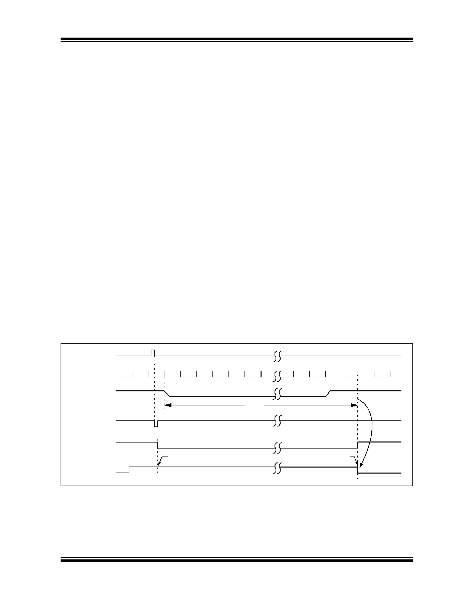
PIC18F2450/4450
� 2006 Microchip Technology Inc.
Advance Information
DS39760A-page 167
15.2.5
BREAK CHARACTER SEQUENCE
The EUSART module has the capability of sending the
special Break character sequences that are required by
the LIN bus standard. The Break character transmit
consists of a Start bit, followed by twelve `0' bits and a
Stop bit. The Frame Break character is sent whenever
the SENDB and TXEN bits (TXSTA<3> and
TXSTA<5>) are set while the Transmit Shift Register is
loaded with data. Note that the value of data written to
TXREG will be ignored and all `0's will be transmitted.
The SENDB bit is automatically reset by hardware after
the corresponding Stop bit is sent. This allows the user
to preload the transmit FIFO with the next transmit byte
following the Break character (typically, the Sync
character in the LIN specification).
Note that the data value written to the TXREG for the
Break character is ignored. The write simply serves the
purpose of initiating the proper sequence.
The TRMT bit indicates when the transmit operation is
active or Idle, just as it does during normal transmission.
See Figure 15-10 for the timing of the Break character
sequence.
15.2.5.1
Break and Sync Transmit Sequence
The following sequence will send a message frame
header made up of a Break, followed by an Auto-Baud
Sync byte. This sequence is typical of a LIN bus master.
1.
Configure the EUSART for the desired mode.
2.
Set the TXEN and SENDB bits to set up the
Break character.
3.
Load the TXREG with a dummy character to
initiate transmission (the value is ignored).
4.
Write `55h' to TXREG to load the Sync character
into the transmit FIFO buffer.
5.
After the Break has been sent, the SENDB bit is
reset by hardware. The Sync character now
transmits in the preconfigured mode.
When the TXREG becomes empty, as indicated by the
TXIF, the next data byte can be written to TXREG.
15.2.6
RECEIVING A BREAK CHARACTER
The Enhanced USART module can receive a Break
character in two ways.
The first method forces configuration of the baud rate
at a frequency of 9/13 the typical speed. This allows for
the Stop bit transition to be at the correct sampling
location (13 bits for Break versus Start bit and eight
data bits for typical data).
The second method uses the auto-wake-up feature
described in Section 15.2.4 "Auto-Wake-up on Sync
Break Character". By enabling this feature, the
EUSART will sample the next two transitions on RX/DT,
cause an RCIF interrupt and receive the next data byte
followed by another interrupt.
Note that following a Break character, the user will
typically want to enable the Auto-Baud Rate Detect
feature. For both methods, the user can set the ABD bit
once the TXIF interrupt is observed.
FIGURE 15-10:
SEND BREAK CHARACTER SEQUENCE
Write to TXREG
BRG Output
(Shift Clock)
Start bit
bit 0
bit 1
bit 11
Stop bit
Break
TXIF bit
(Transmit Buffer
Reg. Empty Flag)
TX (pin)
TRMT bit
(Transmit Shift
Reg. Empty Flag)
SENDB
(Transmit Shift
Reg. Empty Flag)
SENDB sampled here
Auto-Cleared
Dummy Write
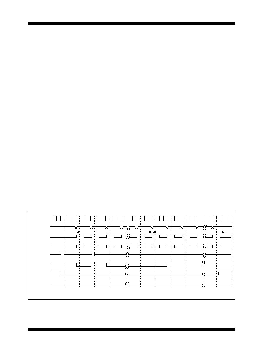
PIC18F2450/4450
DS39760A-page 168
Advance Information
� 2006 Microchip Technology Inc.
15.3
EUSART Synchronous
Master Mode
The Synchronous Master mode is entered by setting
the CSRC bit (TXSTA<7>). In this mode, the data is
transmitted in a half-duplex manner (i.e., transmission
and reception do not occur at the same time). When
transmitting data, the reception is inhibited and vice
versa. Synchronous mode is entered by setting bit,
SYNC (TXSTA<4>). In addition, enable bit, SPEN
(RCSTA<7>), is set in order to configure the TX and RX
pins to CK (clock) and DT (data) lines, respectively.
The Master mode indicates that the processor
transmits the master clock on the CK line. Clock
polarity is selected with the SCKP bit (BAUDCON<4>).
Setting SCKP sets the Idle state on CK as high, while
clearing the bit sets the Idle state as low. This option is
provided to support Microwire devices with this module.
15.3.1
EUSART SYNCHRONOUS MASTER
TRANSMISSION
The EUSART transmitter block diagram is shown in
Figure 15-3. The heart of the transmitter is the Transmit
(Serial) Shift Register (TSR). The Shift register obtains
its data from the Read/Write Transmit Buffer register,
TXREG. The TXREG register is loaded with data in
software. The TSR register is not loaded until the last
bit has been transmitted from the previous load. As
soon as the last bit is transmitted, the TSR is loaded
with new data from the TXREG (if available).
Once the TXREG register transfers the data to the TSR
register (occurs in one T
CYCLE
), the TXREG register is
empty and the TXIF flag bit (PIR1<4>) is set. The
interrupt can be enabled or disabled by setting or
clearing the interrupt enable bit, TXIE (PIE1<4>). TXIF
is set regardless of the state of enable bit TXIE; it
cannot be cleared in software. It will reset only when
new data is loaded into the TXREG register.
While flag bit, TXIF, indicates the status of the TXREG
register, another bit, TRMT (TXSTA<1>), shows the
status of the TSR register. TRMT is a read-only bit which
is set when the TSR is empty. No interrupt logic is tied to
this bit so the user must poll this bit in order to determine
if the TSR register is empty. The TSR is not mapped in
data memory so it is not available to the user.
To set up a Synchronous Master Transmission:
1.
Initialize the SPBRGH:SPBRG registers for the
appropriate baud rate. Set or clear the BRG16
bit, as required, to achieve the desired baud
rate.
2.
Enable the synchronous master serial port by
setting bits SYNC, SPEN and CSRC.
3.
If interrupts are desired, set enable bit TXIE.
4.
If 9-bit transmission is desired, set bit TX9.
5.
Enable the transmission by setting bit TXEN.
6.
If 9-bit transmission is selected, the ninth bit
should be loaded in bit TX9D.
7.
Start transmission by loading data to the TXREG
register.
8.
If using interrupts, ensure that the GIE and PEIE
bits in the INTCON register (INTCON<7:6>) are
set.
FIGURE 15-11:
SYNCHRONOUS TRANSMISSION
bit 0
bit 1
bit 7
Word 1
Q1 Q2 Q3Q4 Q1 Q2 Q3 Q4 Q1 Q2 Q3 Q4 Q1Q2 Q3 Q4 Q1 Q2 Q3 Q4
Q3 Q4 Q1 Q2 Q3 Q4 Q1Q2 Q3 Q4 Q1 Q2 Q3 Q4 Q1 Q2 Q3 Q4 Q1 Q2 Q3 Q4 Q1 Q2 Q3 Q4
bit 2
bit 0
bit 1
bit 7
RC7/RX/DT pin
RC6/TX/CK pin
Write to
TXREG Reg
TXIF bit
(Interrupt Flag)
TXEN bit
`1'
`1'
Word 2
TRMT bit
Write Word 1
Write Word 2
Note:
Sync Master mode (SPBRG = 0), continuous transmission of two 8-bit words.
RC6/TX/CK pin
(SCKP = 0)
(SCKP = 1)
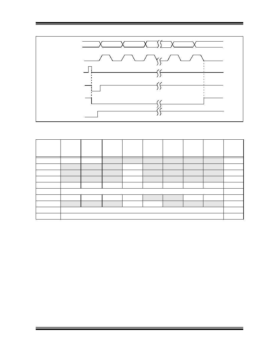
PIC18F2450/4450
� 2006 Microchip Technology Inc.
Advance Information
DS39760A-page 169
FIGURE 15-12:
SYNCHRONOUS TRANSMISSION (THROUGH TXEN)
TABLE 15-7:
REGISTERS ASSOCIATED WITH SYNCHRONOUS MASTER TRANSMISSION
RC7/RX/DT pin
RC6/TX/CK pin
Write to
TXREG reg
TXIF bit
TRMT bit
bit 0
bit 1
bit 2
bit 6
bit 7
TXEN bit
Name
Bit 7
Bit 6
Bit 5
Bit 4
Bit 3
Bit 2
Bit 1
Bit 0
Reset
Values
on page
INTCON
GIE/GIEH PEIE/GIEL
TMR0IE
INT0IE
RBIE
TMR0IF
INT0IF
RBIF
49
PIR1
--
ADIF
RCIF
TXIF
--
CCP1IF
TMR2IF
TMR1IF
51
PIE1
--
ADIE
RCIE
TXIE
--
CCP1IE
TMR2IE
TMR1IE
51
IPR1
--
ADIP
RCIP
TXIP
--
CCP1IP
TMR2IP
TMR1IP
51
RCSTA
SPEN
RX9
SREN
CREN
ADDEN
FERR
OERR
RX9D
51
TXREG
EUSART Transmit Register
50
TXSTA
CSRC
TX9
TXEN
SYNC
SENDB
BRGH
TRMT
TX9D
51
BAUDCON
ABDOVF
RCIDL
--
SCKP
BRG16
--
WUE
ABDEN
51
SPBRGH
EUSART Baud Rate Generator Register High Byte
50
SPBRG
EUSART Baud Rate Generator Register Low Byte
50
Legend: -- = unimplemented, read as `0'. Shaded cells are not used for synchronous master transmission.
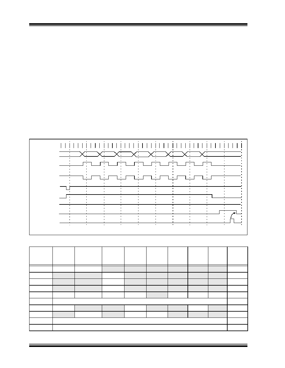
PIC18F2450/4450
DS39760A-page 170
Advance Information
� 2006 Microchip Technology Inc.
15.3.2
EUSART SYNCHRONOUS MASTER
RECEPTION
Once Synchronous mode is selected, reception is
enabled by setting either the Single Receive Enable bit,
SREN (RCSTA<5>), or the Continuous Receive
Enable bit, CREN (RCSTA<4>). Data is sampled on the
RX pin on the falling edge of the clock.
If enable bit SREN is set, only a single word is received.
If enable bit CREN is set, the reception is continuous
until CREN is cleared. If both bits are set, then CREN
takes precedence.
To set up a Synchronous Master Reception:
1.
Initialize the SPBRGH:SPBRG registers for the
appropriate baud rate. Set or clear the BRG16
bit, as required, to achieve the desired baud rate.
2.
Enable the synchronous master serial port by
setting bits SYNC, SPEN and CSRC.
3.
Ensure bits CREN and SREN are clear.
4.
If interrupts are desired, set enable bit RCIE.
5.
If 9-bit reception is desired, set bit RX9.
6.
If a single reception is required, set bit SREN.
For continuous reception, set bit CREN.
7.
Interrupt flag bit RCIF will be set when reception
is complete and an interrupt will be generated if
the enable bit RCIE was set.
8.
Read the RCSTA register to get the ninth bit (if
enabled) and determine if any error occurred
during reception.
9.
Read the 8-bit received data by reading the
RCREG register.
10. If any error occurred, clear the error by clearing
bit CREN.
11. If using interrupts, ensure that the GIE and PEIE
bits in the INTCON register (INTCON<7:6>) are
set.
FIGURE 15-13:
SYNCHRONOUS RECEPTION (MASTER MODE, SREN)
TABLE 15-8:
REGISTERS ASSOCIATED WITH SYNCHRONOUS MASTER RECEPTION
Name
Bit 7
Bit 6
Bit 5
Bit 4
Bit 3
Bit 2
Bit 1
Bit 0
Reset
Values
on page
INTCON
GIE/GIEH
PEIE/GIEL
TMR0IE
INT0IE
RBIE
TMR0IF
INT0IF
RBIF
49
PIR1
--
ADIF
RCIF
TXIF
--
CCP1IF
TMR2IF
TMR1IF
51
PIE1
--
ADIE
RCIE
TXIE
--
CCP1IE
TMR2IE
TMR1IE
51
IPR1
--
ADIP
RCIP
TXIP
--
CCP1IP
TMR2IP
TMR1IP
51
RCSTA
SPEN
RX9
SREN
CREN
ADDEN
FERR
OERR
RX9D
51
RCREG
EUSART Receive Register
50
TXSTA
CSRC
TX9
TXEN
SYNC
SENDB
BRGH
TRMT
TX9D
51
BAUDCON ABDOVF
RCIDL
--
SCKP
BRG16
--
WUE
ABDEN
51
SPBRGH
EUSART Baud Rate Generator Register High Byte
51
SPBRG
EUSART Baud Rate Generator Register Low Byte
50
Legend: -- = unimplemented, read as `0'. Shaded cells are not used for synchronous master reception.
CREN bit
RC7/RX/DT
RC6/TX/CK pin
Write to
bit SREN
SREN bit
RCIF bit
(Interrupt)
Read
RXREG
Q3 Q4 Q1 Q2 Q3 Q4 Q1 Q2 Q3 Q4
Q2
Q1 Q2 Q3 Q4 Q1 Q2 Q3 Q4 Q1 Q2 Q3 Q4 Q1 Q2 Q3 Q4 Q1 Q2 Q3 Q4 Q1 Q2 Q3 Q4 Q1 Q2 Q3 Q4
`0'
bit 0
bit 1
bit 2
bit 3
bit 4
bit 5
bit 6
bit 7
`0'
Q1 Q2 Q3 Q4
Note:
Timing diagram demonstrates Sync Master mode with bit SREN = 1 and bit BRGH = 0.
RC6/TX/CK pin
pin
(SCKP = 0)
(SCKP = 1)
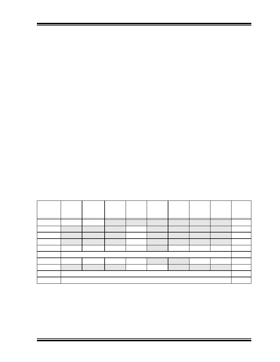
PIC18F2450/4450
� 2006 Microchip Technology Inc.
Advance Information
DS39760A-page 171
15.4
EUSART Synchronous
Slave Mode
Synchronous Slave mode is entered by clearing bit,
CSRC (TXSTA<7>). This mode differs from the
Synchronous Master mode in that the shift clock is
supplied externally at the CK pin (instead of being
supplied internally in Master mode). This allows the
device to transfer or receive data while in any low-power
mode.
15.4.1
EUSART SYNCHRONOUS
SLAVE TRANSMIT
The operation of the Synchronous Master and Slave
modes is identical, except in the case of Sleep mode.
If two words are written to the TXREG register and then
the SLEEP instruction is executed, the following will occur:
a)
The first word will immediately transfer to the
TSR register and transmit.
b)
The second word will remain in the TXREG
register.
c)
Flag bit TXIF will not be set.
d)
When the first word has been shifted out of TSR,
the TXREG register will transfer the second word
to the TSR and flag bit TXIF will now be set.
e)
If enable bit TXIE is set, the interrupt will wake the
chip from Sleep. If the global interrupt is enabled,
the program will branch to the interrupt vector.
To set up a Synchronous Slave Transmission:
1.
Enable the synchronous slave serial port by
setting bits SYNC and SPEN and clearing bit
CSRC.
2.
Clear bits CREN and SREN.
3.
If interrupts are desired, set enable bit TXIE.
4.
If 9-bit transmission is desired, set bit TX9.
5.
Enable the transmission by setting enable bit
TXEN.
6.
If 9-bit transmission is selected, the ninth bit
should be loaded in bit TX9D.
7.
Start transmission by loading data to the TXREG
register.
8.
If using interrupts, ensure that the GIE and PEIE
bits in the INTCON register (INTCON<7:6>) are
set.
TABLE 15-9:
REGISTERS ASSOCIATED WITH SYNCHRONOUS SLAVE TRANSMISSION
Name
Bit 7
Bit 6
Bit 5
Bit 4
Bit 3
Bit 2
Bit 1
Bit 0
Reset
Values
on page
INTCON
GIE/GIEH PEIE/GIEL
TMR0IE
INT0IE
RBIE
TMR0IF
INT0IF
RBIF
49
PIR1
--
ADIF
RCIF
TXIF
--
CCP1IF
TMR2IF
TMR1IF
51
PIE1
--
ADIE
RCIE
TXIE
--
CCP1IE
TMR2IE
TMR1IE
51
IPR1
--
ADIP
RCIP
TXIP
--
CCP1IP
TMR2IP
TMR1IP
51
RCSTA
SPEN
RX9
SREN
CREN
ADDEN
FERR
OERR
RX9D
51
TXREG
EUSART Transmit Register
50
TXSTA
CSRC
TX9
TXEN
SYNC
SENDB
BRGH
TRMT
TX9D
51
BAUDCON
ABDOVF
RCIDL
--
SCKP
BRG16
--
WUE
ABDEN
51
SPBRGH
EUSART
Baud Rate Generator Register High Byte
50
SPBRG
EUSART Baud Rate Generator Register Low Byte
50
Legend: -- = unimplemented, read as `0'. Shaded cells are not used for synchronous slave transmission.

PIC18F2450/4450
DS39760A-page 172
Advance Information
� 2006 Microchip Technology Inc.
15.4.2
EUSART SYNCHRONOUS SLAVE
RECEPTION
The operation of the Synchronous Master and Slave
modes is identical, except in the case of Sleep or any
Idle mode and bit SREN, which is a "don't care" in
Slave mode.
If receive is enabled by setting the CREN bit prior to
entering Sleep or any Idle mode, then a word may be
received while in this low-power mode. Once the word
is received, the RSR register will transfer the data to the
RCREG register. If the RCIE enable bit is set, the
interrupt generated will wake the chip from the low-
power mode. If the global interrupt is enabled, the
program will branch to the interrupt vector.
To set up a Synchronous Slave Reception:
1.
Enable the synchronous master serial port by
setting bits SYNC and SPEN and clearing bit
CSRC.
2.
If interrupts are desired, set enable bit RCIE.
3.
If 9-bit reception is desired, set bit RX9.
4.
To enable reception, set enable bit CREN.
5.
Flag bit RCIF will be set when reception is
complete. An interrupt will be generated if
enable bit RCIE was set.
6.
Read the RCSTA register to get the ninth bit (if
enabled) and determine if any error occurred
during reception.
7.
Read the 8-bit received data by reading the
RCREG register.
8.
If any error occurred, clear the error by clearing
bit CREN.
9.
If using interrupts, ensure that the GIE and PEIE
bits in the INTCON register (INTCON<7:6>) are
set.
TABLE 15-10: REGISTERS ASSOCIATED WITH SYNCHRONOUS SLAVE RECEPTION
Name
Bit 7
Bit 6
Bit 5
Bit 4
Bit 3
Bit 2
Bit 1
Bit 0
Reset
Values
on page
INTCON
GIE/GIEH PEIE/GIEL
TMR0IE
INT0IE
RBIE
TMR0IF
INT0IF
RBIF
49
PIR1
--
ADIF
RCIF
TXIF
--
CCP1IF
TMR2IF
TMR1IF
51
PIE1
--
ADIE
RCIE
TXIE
--
CCP1IE
TMR2IE
TMR1IE
51
IPR1
--
ADIP
RCIP
TXIP
--
CCP1IP
TMR2IP
TMR1IP
51
RCSTA
SPEN
RX9
SREN
CREN
ADDEN
FERR
OERR
RX9D
51
RCREG
EUSART Receive Register
50
TXSTA
CSRC
TX9
TXEN
SYNC
SENDB
BRGH
TRMT
TX9D
51
BAUDCON
ABDOVF
RCIDL
--
SCKP
BRG16
--
WUE
ABDEN
51
SPBRGH
EUSART Baud Rate Generator Register High Byte
50
SPBRG
EUSART Baud Rate Generator Register Low Byte
50
Legend: -- = unimplemented, read as `0'. Shaded cells are not used for synchronous slave reception.

PIC18F2450/4450
� 2006 Microchip Technology Inc.
Advance Information
DS39760A-page 173
16.0
10-BIT ANALOG-TO-DIGITAL
CONVERTER (A/D) MODULE
The Analog-to-Digital (A/D) converter module has
10 inputs for the 28-pin devices and 13 for the 40/44-pin
devices. This module allows conversion of an analog
input signal to a corresponding 10-bit digital number.
The module has five registers:
� A/D Result High Register (ADRESH)
� A/D Result Low Register (ADRESL)
� A/D Control Register 0 (ADCON0)
� A/D Control Register 1 (ADCON1)
� A/D Control Register 2 (ADCON2)
The ADCON0 register, shown in Register 16-1,
controls the operation of the A/D module. The
ADCON1 register, shown in Register 16-2, configures
the functions of the port pins. The ADCON2 register,
shown in Register 16-3, configures the A/D clock
source, programmed acquisition time and justification.
REGISTER 16-1:
ADCON0: A/D CONTROL REGISTER 0
U0
U-0
R/W-0
R/W-0
R/W-0
R/W-0
R/W-0
R/W-0
--
--
CHS3
CHS2
CHS1
CHS0
GO/DONE
ADON
bit 7
bit 0
Legend:
R = Readable bit
W = Writable bit
U = Unimplemented bit, read as `0'
-n = Value at POR
`1' = Bit is set
`0' = Bit is cleared
x = Bit is unknown
bit 7-6
Unimplemented: Read as `0'
bit 5-2
CHS3:CHS0: Analog Channel Select bits
0000
= Channel 0 (AN0)
0001
= Channel 1 (AN1)
0010
= Channel 2 (AN2)
0011
= Channel 3 (AN3)
0100
= Channel 4 (AN4)
0101
= Channel 5 (AN5)
(1,2)
0110
= Channel 6 (AN6)
(1,2)
0111
= Channel 7 (AN7)
(1,2)
1000
= Channel 8 (AN8)
1001
= Channel 9 (AN9)
1010
= Channel 10 (AN10)
1011
= Channel 11 (AN11)
1100
= Channel 12 (AN12
1101
= Unimplemented
(2)
1110
= Unimplemented
(2)
1111
= Unimplemented
(2)
bit 1
GO/DONE: A/D Conversion Status bit
When ADON = 1:
1
= A/D conversion in progress
0
= A/D Idle
bit 0
ADON: A/D On bit
1
= A/D converter module is enabled
0
= A/D converter module is disabled
Note 1:
These channels are not implemented on 28-pin devices.
2:
Performing a conversion on unimplemented channels will return a floating input measurement.

PIC18F2450/4450
DS39760A-page 174
Advance Information
� 2006 Microchip Technology Inc.
REGISTER 16-2:
ADCON1: A/D CONTROL REGISTER 1
U-0
U-0
R/W-0
R/W-0
R/W-0
(1)
R/W
(1)
R/W
(1)
R/W
(1)
--
--
VCFG0
VCFG0
PCFG3
PCFG2
PCFG1
PCFG0
bit 7
bit 0
Legend:
R = Readable bit
W = Writable bit
U = Unimplemented bit, read as `0'
-n = Value at POR
`1' = Bit is set
`0' = Bit is cleared
x = Bit is unknown
bit 7-6
Unimplemented: Read as `0'
bit 5
VCFG0: Voltage Reference Configuration bit (V
REF
- source)
1
= V
REF
- (AN2)
0
= V
SS
bit 4
VCFG0: Voltage Reference Configuration bit (V
REF
+ source)
1
= V
REF
+ (AN3)
0
= V
DD
bit 3-0
PCFG3:PCFG0: A/D Port Configuration Control bits:
Note 1:
The POR value of the PCFG bits depends on the value of the PBADEN
Configuration bit. When PBADEN = 1, PCFG<3:0> = 0000; when PBADEN = 0, PCFG<3:0> = 0111.
2:
AN5 through AN7 are available only on 40/44-pin devices.
A = Analog input
D = Digital I/O
PCFG3:
PCFG0
AN1
2
AN1
1
AN1
0
AN9
AN8
AN7
(2
)
AN6
(2
)
AN5
(2
)
AN4
AN3
AN2
AN1
AN0
0000
(1)
A
A
A
A
A
A
A
A
A
A
A
A
A
0001
A
A
A
A
A
A
A
A
A
A
A
A
A
0010
A
A
A
A
A
A
A
A
A
A
A
A
A
0011
D
A
A
A
A
A
A
A
A
A
A
A
A
0100
D
D
A
A
A
A
A
A
A
A
A
A
A
0101
D
D
D
A
A
A
A
A
A
A
A
A
A
0110
D
D
D
D
A
A
A
A
A
A
A
A
A
0111
(1)
D
D
D
D
D
A
A
A
A
A
A
A
A
1000
D
D
D
D
D
D
A
A
A
A
A
A
A
1001
D
D
D
D
D
D
D
A
A
A
A
A
A
1010
D
D
D
D
D
D
D
D
A
A
A
A
A
1011
D
D
D
D
D
D
D
D
D
A
A
A
A
1100
D
D
D
D
D
D
D
D
D
D
A
A
A
1101
D
D
D
D
D
D
D
D
D
D
D
A
A
1110
D
D
D
D
D
D
D
D
D
D
D
D
A
1111
D
D
D
D
D
D
D
D
D
D
D
D
D

PIC18F2450/4450
� 2006 Microchip Technology Inc.
Advance Information
DS39760A-page 175
REGISTER 16-3:
ADCON2: A/D CONTROL REGISTER 2
R/W-0
U-0
R/W-0
R/W-0
R/W-0
R/W-0
R/W-0
R/W-0
ADFM
--
ACQT2
ACQT1
ACQT0
ADCS2
ADCS1
ADCS0
bit 7
bit 0
Legend:
R = Readable bit
W = Writable bit
U = Unimplemented bit, read as `0'
-n = Value at POR
`1' = Bit is set
`0' = Bit is cleared
x = Bit is unknown
bit 7
ADFM: A/D Result Format Select bit
1
= Right justified
0
= Left justified
bit 6
Unimplemented: Read as `0'
bit 5-3
ACQT2:ACQT0: A/D Acquisition Time Select bits
111
= 20 T
AD
110
= 16 T
AD
101
= 12 T
AD
100
= 8 T
AD
011
= 6 T
AD
010
= 4 T
AD
001
= 2 T
AD
000
= 0 T
AD
(1)
bit 2-0
ADCS2:ADCS0: A/D Conversion Clock Select bits
111
= F
RC
(clock derived from A/D RC oscillator)
(1)
110
= F
OSC
/64
101
= F
OSC
/16
100
= F
OSC
/4
011
= F
RC
(clock derived from A/D RC oscillator)
(1)
010
= F
OSC
/32
001
= F
OSC
/8
000
= F
OSC
/2
Note 1:
If the A/D F
RC
clock source is selected, a delay of one T
CY
(instruction cycle) is added before the A/D
clock starts. This allows the SLEEP instruction to be executed before starting a conversion.
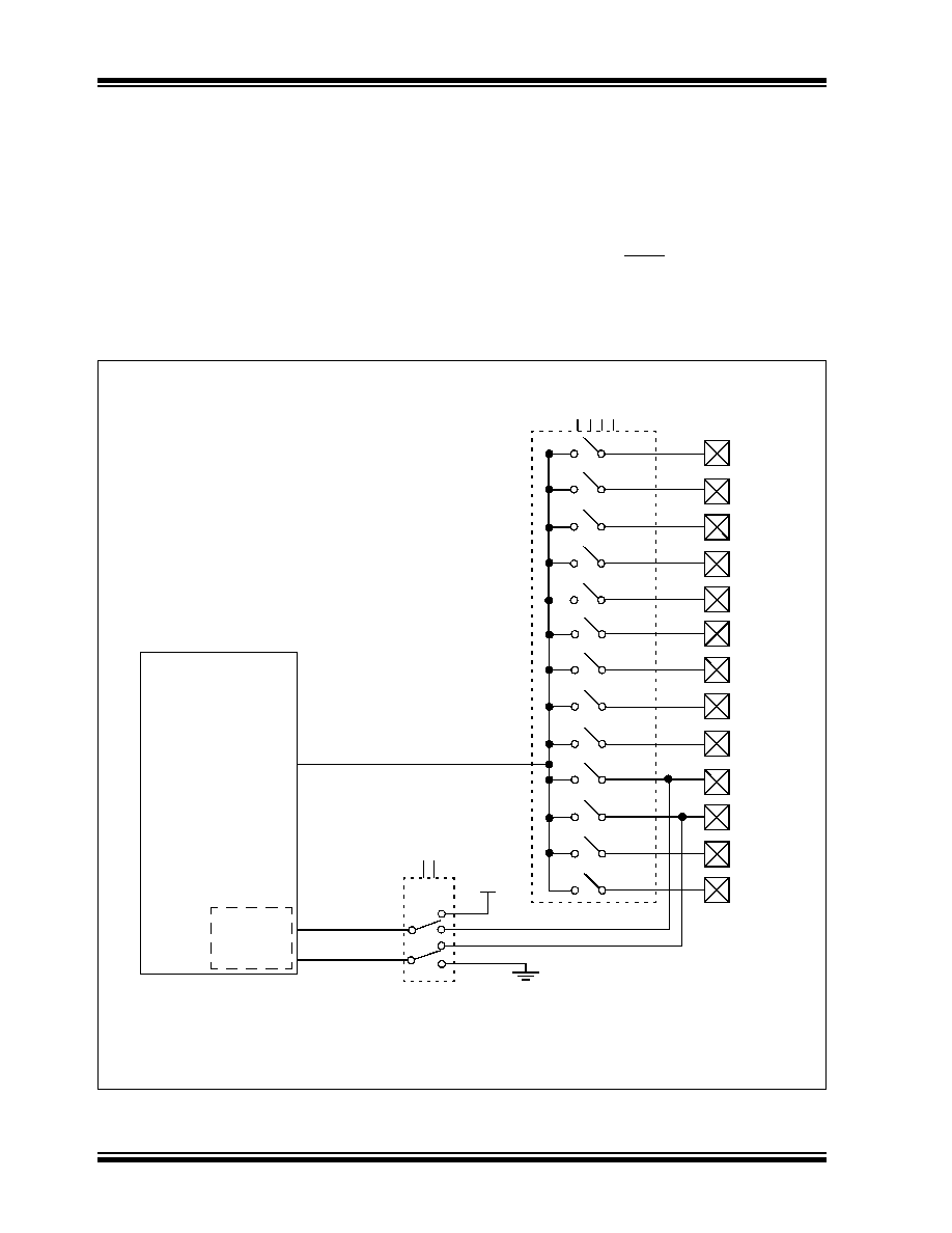
PIC18F2450/4450
DS39760A-page 176
Advance Information
� 2006 Microchip Technology Inc.
The analog reference voltage is software selectable to
either the device's positive and negative supply voltage
(V
DD
and V
SS
) or the voltage level on the RA3/AN3/
V
REF
+ and RA2/AN2/V
REF
- pins.
The A/D converter has a unique feature of being able
to operate while the device is in Sleep mode. To
operate in Sleep, the A/D conversion clock must be
derived from the A/D's internal RC oscillator.
The output of the sample and hold is the input into the
converter, which generates the result via successive
approximation.
A device Reset forces all registers to their Reset state.
This forces the A/D module to be turned off and any
conversion in progress is aborted.
Each port pin associated with the A/D converter can be
configured as an analog input or as a digital I/O. The
ADRESH and ADRESL registers contain the result of
the A/D conversion. When the A/D conversion is com-
plete, the result is loaded into the ADRESH:ADRESL
register pair, the GO/DONE bit (ADCON0 register) is
cleared and A/D Interrupt Flag bit, ADIF, is set. The block
diagram of the A/D module is shown in Figure 16-1.
FIGURE 16-1:
A/D BLOCK DIAGRAM
(Input Voltage)
V
AIN
V
REF
+
Reference
Voltage
V
DD
(2)
VCFG1:VCFG0
CHS3:CHS0
AN7
(1)
AN6
(1)
AN5
(1)
AN4
AN3
AN2
AN1
AN0
0111
0110
0101
0100
0011
0010
0001
0000
10-Bit
Converter
V
REF
-
V
SS
(2)
A/D
AN12
AN11
AN10
AN9
AN8
1100
1011
1010
1001
1000
Note 1:
Channels AN5 through AN7 are not available on 28-pin devices.
2:
I/O pins have diode protection to V
DD
and V
SS
.
0
X
1
X
X
1
X
0
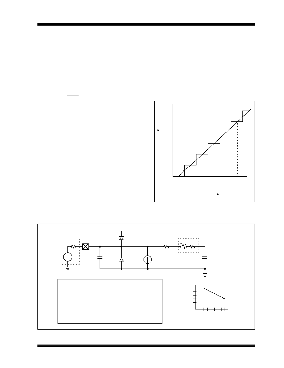
PIC18F2450/4450
� 2006 Microchip Technology Inc.
Advance Information
DS39760A-page 177
The value in the ADRESH:ADRESL registers is not
modified for a Power-on Reset. The ADRESH:ADRESL
registers will contain unknown data after a Power-on
Reset.
After the A/D module has been configured as desired, the
selected channel must be acquired before the conver-
sion is started. The analog input channels must have
their corresponding TRIS bits selected as an input. To
determine acquisition time, see Section 16.1 "A/D
Acquisition Requirements". After this acquisition time
has elapsed, the A/D conversion can be started. An
acquisition time can be programmed to occur between
setting the GO/DONE bit and the actual start of the
conversion.
The following steps should be followed to perform an
A/D conversion:
1.
Configure the A/D module:
� Configure analog pins, voltage reference and
digital I/O (ADCON1)
� Select A/D input channel (ADCON0)
� Select A/D acquisition time (ADCON2)
� Select A/D conversion clock (ADCON2)
� Turn on A/D module (ADCON0)
2.
Configure A/D interrupt (if desired):
� Clear ADIF bit
� Set ADIE bit
� Set GIE bit
3.
Wait the required acquisition time (if required).
4.
Start conversion:
� Set GO/DONE bit (ADCON0 register)
5.
Wait for A/D conversion to complete, by either:
� Polling for the GO/DONE bit to be cleared
OR
� Waiting for the A/D interrupt
6.
Read A/D Result registers (ADRESH:ADRESL);
clear bit ADIF, if required.
7.
For next conversion, go to step 1 or step 2, as
required. The A/D conversion time per bit is
defined as T
AD
. A minimum wait of 3 T
AD
is
required before the next acquisition starts.
FIGURE 16-2:
A/D TRANSFER FUNCTION
FIGURE 16-3:
ANALOG INPUT MODEL
Dig
it
a
l
Co
d
e
Ou
tp
u
t
3FEh
003h
002h
001h
000h
0.
5
LS
B
1 L
S
B
1.
5
LS
B
2 L
S
B
2.
5
LS
B
102
2 L
S
B
10
22
.5 L
S
B
3 L
S
B
Analog Input Voltage
3FFh
102
3 L
S
B
10
23
.5 L
S
B
V
AIN
C
PIN
Rs
ANx
5 pF
V
T
= 0.6V
V
T
= 0.6V
I
LEAKAGE
R
IC
1k
Sampling
Switch
SS
R
SS
C
HOLD
= 25 pF
V
SS
V
DD
�100 nA
Legend: C
PIN
V
T
I
LEAKAGE
R
IC
SS
C
HOLD
= Input Capacitance
= Threshold Voltage
= Leakage Current at the pin due to
= Interconnect Resistance
= Sampling Switch
= Sample/hold Capacitance (from DAC)
various junctions
= Sampling Switch Resistance
R
SS
V
DD
6V
Sampling Switch
5V
4V
3V
2V
1
2
3
4
(k
)

PIC18F2450/4450
DS39760A-page 178
Advance Information
� 2006 Microchip Technology Inc.
16.1
A/D Acquisition Requirements
For the A/D converter to meet its specified accuracy,
the charge holding capacitor (C
HOLD
) must be allowed
to fully charge to the input channel voltage level. The
analog input model is shown in Figure 16-3. The
source impedance (R
S
) and the internal sampling
switch (R
SS
) impedance directly affect the time
required to charge the capacitor C
HOLD
. The sampling
switch (R
SS
) impedance varies over the device voltage
(V
DD
). The source impedance affects the offset voltage
at the analog input (due to pin leakage current). The
maximum recommended impedance for analog
sources is 2.5 k
. After the analog input channel is
selected (changed), the channel must be sampled for
at least the minimum acquisition time before starting a
conversion.
To calculate the minimum acquisition time,
Equation 16-1 may be used. This equation assumes
that 1/2 LSb error is used (1024 steps for the A/D). The
1/2 LSb error is the maximum error allowed for the A/D
to meet its specified resolution.
Example 16-3 shows the calculation of the minimum
required acquisition time T
ACQ
. This calculation is
based on the following application system
assumptions:
C
HOLD
=
25
pF
Rs
=
2.5 k
Conversion Error
1/2 LSb
V
DD
=
5V
R
SS
= 2 k
Temperature
=
85
�C (system max.)
EQUATION 16-1:
ACQUISITION TIME
EQUATION 16-2:
A/D MINIMUM CHARGING TIME
EQUATION 16-3:
CALCULATING THE MINIMUM REQUIRED ACQUISITION TIME
Note:
When the conversion is started, the
holding capacitor is disconnected from the
input pin.
T
ACQ
=
Amplifier Settling Time + Holding Capacitor Charging Time + Temperature Coefficient
=
T
AMP
+ T
C
+ T
COFF
V
HOLD
= (V
REF
� (V
REF
/2048)) � (1 � e
(-T
C
/C
HOLD
(R
IC
+ R
SS
+ R
S
))
)
or
T
C
=
-(C
HOLD
)(R
IC
+ R
SS
+ R
S
) ln(1/2048)
T
ACQ
=
T
AMP
+ T
C
+ T
COFF
T
AMP
=
0.2
s
T
COFF
=
(Temp � 25
�C)(0.02 s/�C)
(85
�C � 25�C)(0.02 s/�C)
1.2
s
Temperature coefficient is only required for temperatures > 25
�C. Below 25�C, T
COFF
= 0 ms.
T
C
=
-(C
HOLD
)(R
IC
+ R
SS
+ R
S
) ln(1/2047)
s
-(25 pF) (1 k
+ 2 k + 2.5 k) ln(0.0004883) s
1.05
s
T
ACQ
=
0.2
s + 1 s + 1.2 s
2.4
s

PIC18F2450/4450
� 2006 Microchip Technology Inc.
Advance Information
DS39760A-page 179
16.2
Selecting and Configuring
Acquisition Time
The ADCON2 register allows the user to select an
acquisition time that occurs each time the GO/DONE
bit is set. It also gives users the option to use an
automatically determined acquisition time.
Acquisition time may be set with the ACQT2:ACQT0
bits (ADCON2<5:3>) which provide a range of 2 to
20 T
AD
. When the GO/DONE bit is set, the A/D module
continues to sample the input for the selected
acquisition time, then automatically begins a
conversion. Since the acquisition time is programmed,
there may be no need to wait for an acquisition time
between selecting a channel and setting the GO/DONE
bit.
Manual acquisition is selected when
ACQT2:ACQT0 = 000. When the GO/DONE bit is set,
sampling is stopped and a conversion begins. The user
is responsible for ensuring the required acquisition time
has passed between selecting the desired input
channel and setting the GO/DONE bit. This option is
also the default Reset state of the ACQT2:ACQT0 bits
and is compatible with devices that do not offer
programmable acquisition times.
In either case, when the conversion is completed, the
GO/DONE bit is cleared, the ADIF flag is set and the
A/D begins sampling the currently selected channel
again. If an acquisition time is programmed, there is
nothing to indicate if the acquisition time has ended or
if the conversion has begun.
16.3
Selecting the A/D Conversion
Clock
The A/D conversion time per bit is defined as T
AD
. The
A/D conversion requires 11 T
AD
per 10-bit conversion.
The source of the A/D conversion clock is software
selectable. There are seven possible options for T
AD
:
� 2 T
OSC
� 4 T
OSC
� 8 T
OSC
� 16 T
OSC
� 32 T
OSC
� 64 T
OSC
� Internal RC Oscillator
For correct A/D conversions, the A/D conversion clock
(T
AD
) must be as short as possible but greater than the
minimum T
AD
(see parameter 130 in Table 21-18 for
more information).
Table 16-1 shows the resultant T
AD
times derived from
the device operating frequencies and the A/D clock
source selected.
TABLE 16-1:
T
AD
vs. DEVICE OPERATING FREQUENCIES
AD Clock Source (T
AD
)
Maximum Device Frequency
Operation
ADCS2:ADCS0
PIC18FXXXX
PIC18LFXXXX
(4)
2 T
OSC
000
2.86 MHz
1.43 kHz
4 T
OSC
100
5.71 MHz
2.86 MHz
8 T
OSC
001
11.43 MHz
5.72 MHz
16 T
OSC
101
22.86 MHz
11.43 MHz
32 T
OSC
010
40.0 MHz
22.86 MHz
64 T
OSC
110
40.0 MHz
22.86 MHz
RC
(3)
x11
1.00 MHz
(1)
1.00 MHz
(2)
Note 1:
The RC source has a typical T
AD
time of 1.2
s.
2:
The RC source has a typical T
AD
time of 2.5
s.
3:
For device frequencies above 1 MHz, the device must be in Sleep for the entire conversion or the A/D
accuracy may be out of specification.
4:
Low-power devices only.

PIC18F2450/4450
DS39760A-page 180
Advance Information
� 2006 Microchip Technology Inc.
16.4
Operation in Power-Managed
Modes
The selection of the automatic acquisition time and
A/D conversion clock is determined in part by the clock
source and frequency while in a power-managed
mode.
If the A/D is expected to operate while the device is in
a power-managed mode, the ACQT2:ACQT0 and
ADCS2:ADCS0 bits in ADCON2 should be updated in
accordance with the clock source to be used in that
mode. After entering the mode, an A/D acquisition or
conversion may be started. Once started, the device
should continue to be clocked by the same clock
source until the conversion has been completed.
If desired, the device may be placed into the
corresponding Idle mode during the conversion. If the
device clock frequency is less than 1 MHz, the A/D RC
clock source should be selected.
Operation in the Sleep mode requires the A/D F
RC
clock to be selected. If bits ACQT2:ACQT0 are set to
`000' and a conversion is started, the conversion will be
delayed one instruction cycle to allow execution of the
SLEEP
instruction and entry to Sleep mode. The IDLEN
bit (OSCCON<7>) must have already been cleared
prior to starting the conversion.
16.5
Configuring Analog Port Pins
The ADCON1, TRISA, TRISB and TRISE registers all
configure the A/D port pins. The port pins needed as
analog inputs must have their corresponding TRIS bits
set (input). If the TRIS bit is cleared (output), the digital
output level (V
OH
or V
OL
) will be converted.
The A/D operation is independent of the state of the
CHS3:CHS0 bits and the TRIS bits.
Note 1: When reading the PORT register, all pins
configured as analog input channels will
read as cleared (a low level). Pins config-
ured as digital inputs will convert as ana-
log inputs. Analog levels on a digitally
configured input will be accurately
converted.
2: Analog levels on any pin defined as a
digital input may cause the digital input
buffer to consume current out of the
device's specification limits.
3: The PBADEN bit in Configuration
Register 3H configures PORTB pins to
reset as analog or digital pins by control-
ling how the PCFG0 bits in ADCON1 are
reset.
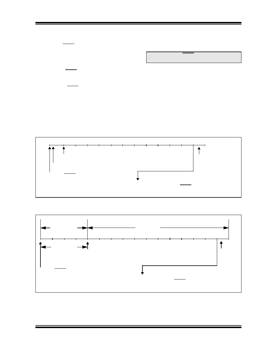
PIC18F2450/4450
� 2006 Microchip Technology Inc.
Advance Information
DS39760A-page 181
16.6
A/D Conversions
Figure 16-4 shows the operation of the A/D converter
after the GO/DONE bit has been set and the
ACQT2:ACQT0 bits are cleared. A conversion is
started after the following instruction to allow entry into
Sleep mode before the conversion begins.
Figure 16-5 shows the operation of the A/D converter
after the GO/DONE bit has been set, the
ACQT2:ACQT0 bits are set to `010' and selecting a
4 T
AD
acquisition time before the conversion starts.
Clearing the GO/DONE bit during a conversion will
abort the current conversion. The A/D Result register
pair will NOT be updated with the partially completed
A/D conversion sample. This means the
ADRESH:ADRESL registers will continue to contain
the value of the last completed conversion (or the last
value written to the ADRESH:ADRESL registers).
After the A/D conversion is completed or aborted, a
2 T
AD
wait is required before the next acquisition can be
started. After this wait, acquisition on the selected
channel is automatically started.
16.7
Discharge
The discharge phase is used to initialize the value of
the capacitor array. The array is discharged before
every sample. This feature helps to optimize the unity-
gain amplifier as the circuit always needs to charge the
capacitor array, rather than charge/discharge based on
previous measurement values.
FIGURE 16-4:
A/D CONVERSION T
AD
CYCLES (ACQT<2:0> = 000, T
ACQ
= 0)
FIGURE 16-5:
A/D CONVERSION T
AD
CYCLES (ACQT<2:0> = 010, T
ACQ
= 4 T
AD
)
Note:
The GO/DONE bit should NOT be set in
the same instruction that turns on the A/D.
T
AD
1 T
AD
2 T
AD
3 T
AD
4 T
AD
5 T
AD
6 T
AD
7 T
AD
8
T
AD
11
Set GO/DONE bit
Holding capacitor is disconnected from analog input (typically 100 ns)
T
AD
9 T
AD
10
T
CY
- T
AD
ADRESH:ADRESL is loaded, GO/DONE bit is cleared,
ADIF bit is set, holding capacitor is connected to analog input.
Conversion starts
b0
b9
b6
b5
b4
b3
b2
b1
b8
b7
On the following cycle:
T
AD
1
Discharge
1
2
3
4
5
6
7
8
11
Set GO/DONE bit
(Holding capacitor is disconnected)
9
10
Conversion starts
1
2
3
4
(Holding capacitor continues
acquiring input)
T
ACQ
Cycles
T
AD
Cycles
Automatic
Acquisition
Time
b0
b9
b6
b5
b4
b3
b2
b1
b8
b7
ADRESH:ADRESL is loaded, GO/DONE bit is cleared,
ADIF bit is set, holding capacitor is connected to analog input.
On the following cycle:
T
AD
1
Discharge

PIC18F2450/4450
DS39760A-page 182
Advance Information
� 2006 Microchip Technology Inc.
16.8
Use of the CCP1 Trigger
An A/D conversion can be started by the Special Event
Trigger of the CCP1 module. This requires that the
CCP1M3:CCP1M0 bits (CCP1CON<3:0>) be
programmed as `1011' and that the A/D module is
enabled (ADON bit is set). When the trigger occurs, the
GO/DONE bit will be set, starting the A/D acquisition
and conversion and the Timer1 counter will be reset to
zero. Timer1 is reset to automatically repeat the A/D
acquisition period with minimal software overhead
(moving ADRESH:ADRESL to the desired location).
The appropriate analog input channel must be selected
and the minimum acquisition period is either timed by
the user, or an appropriate T
ACQ
time selected before
the Special Event Trigger sets the GO/DONE bit (starts
a conversion).
If the A/D module is not enabled (ADON is cleared), the
Special Event Trigger will be ignored by the A/D
module but will still reset the Timer1 counter.
TABLE 16-2:
REGISTERS ASSOCIATED WITH A/D OPERATION
Name
Bit 7
Bit 6
Bit 5
Bit 4
Bit 3
Bit 2
Bit 1
Bit 0
Reset
Values
on page
INTCON
GIE/GIEH PEIE/GIEL
TMR0IE
INT0IE
RBIE
TMR0IF
INT0IF
RBIF
49
PIR1
--
ADIF
RCIF
TXIF
--
CCP1IF
TMR2IF
TMR1IF
51
PIE1
--
ADIE
RCIE
TXIE
--
CCP1IE
TMR2IE
TMR1IE
51
IPR1
--
ADIP
RCIP
TXIP
--
CCP1IP
TMR2IP
TMR1IP
51
PIR2
OSCFIF
--
USBIF
--
--
HLVDIF
--
--
51
PIE2
OSCFIE
--
USBIE
--
--
HLVDIE
--
--
51
IPR2
OSCFIP
--
USBIP
--
--
HLVDIP
--
--
51
ADRESH
A/D Result Register High Byte
50
ADRESL
A/D Result Register Low Byte
50
ADCON0
--
--
CHS3
CHS2
CHS1
CHS0
GO/DONE
ADON
50
ADCON1
--
--
VCFG1
VCFG0
PCFG3
PCFG2
PCFG1
PCFG0
50
ADCON2
ADFM
--
ACQT2
ACQT1
ACQT0
ADCS2
ADCS1
ADCS0
50
PORTA
--
RA6
(2)
RA5
RA4
RA3
RA2
RA1
RA0
51
TRISA
--
TRISA6
(2)
TRISA5
TRISA4
TRISA3
TRISA2
TRISA1
TRISA0
51
PORTB
RB7
RB6
RB5
RB4
RB3
RB2
RB1
RB0
51
TRISB
TRISB7
TRISB6
TRISB5
TRISB4
TRISB3
TRISB2
TRISB1
TRISB0
51
LATB
LATB7
LATB6
LATB5
LATB4
LATB3
LATB2
LATB1
LATB0
51
PORTE
--
--
--
--
RE3
(1,3)
RE2
(4)
RE1
(4)
RE0
(4)
51
TRISE
(4)
--
--
--
--
--
TRISE2
(4)
TRISE1
(4)
TRISE0
(4)
51
LATE
(4)
--
--
--
--
--
LATE2
(4)
LATE1
(4)
LATE0
(4)
51
Legend: -- = unimplemented, read as `0'. Shaded cells are not used for A/D conversion.
Note 1:
Implemented only when Master Clear functionality is disabled (MCLRE Configuration bit = 0).
2:
RA6 and its associated latch and data direction bits are enabled as I/O pins based on oscillator
configuration; otherwise, they are read as `0'.
3:
RE3 port bit is available only as an input pin when the MCLRE Configuration bit is `0'.
4:
These registers and/or bits are not implemented on 28-pin devices.

PIC18F2450/4450
� 2006 Microchip Technology Inc.
Advance Information
DS39760A-page 183
17.0
HIGH/LOW-VOLTAGE DETECT
(HLVD)
PIC18F2450/4450 devices have a High/Low-Voltage
Detect module (HLVD). This is a programmable circuit
that allows the user to specify both a device voltage trip
point and the direction of change from that point. If the
device experiences an excursion past the trip point in
that direction, an interrupt flag is set. If the interrupt is
enabled, the program execution will branch to the
interrupt vector address and the software can then
respond to the interrupt.
The High/Low-Voltage Detect Control register
(Register 17-1) completely controls the operation of the
HLVD module. This allows the circuitry to be "turned
off" by the user under software control which minimizes
the current consumption for the device.
The block diagram for the HLVD module is shown in
Figure 17-1.
REGISTER 17-1:
HLVDCON: HIGH/LOW-VOLTAGE DETECT CONTROL REGISTER
R/W-0
U-0
R-0
R/W-0
R/W-0
R/W-1
R/W-0
R/W-1
VDIRMAG
--
IRVST
HLVDEN
HLVDL3
(1)
HLVDL2
(1)
HLVDL1
(1)
HLVDL0
(1)
bit 7
bit 0
Legend:
R = Readable bit
W = Writable bit
U = Unimplemented bit, read as `0'
-n = Value at POR
`1' = Bit is set
`0' = Bit is cleared
x = Bit is unknown
bit 7
VDIRMAG: Voltage Direction Magnitude Select bit
1
= Event occurs when voltage equals or exceeds trip point (HLVDL3:HLDVL0)
0
= Event occurs when voltage equals or falls below trip point (HLVDL3:HLVDL0)
bit 6
Unimplemented: Read as `0'
bit 5
IRVST: Internal Reference Voltage Stable Flag bit
1
= Indicates that the voltage detect logic will generate the interrupt flag at the specified voltage
trip point
0
= Indicates that the voltage detect logic will not generate the interrupt flag at the specified voltage
trip point and the LVD interrupt should not be enabled
bit 4
HLVDEN: High/Low-Voltage Detect Power Enable bit
1
= HLVD enabled
0
= HLVD disabled
bit 3-0
HLVDL3:HLVDL0: Voltage Detection Limit bits
(1)
1111
= Reserved
1110
= Maximum setting
.
.
.
0000
= Minimum setting
Note 1:
See Table 21-4 in Section 21.0 "Electrical Characteristics" for specifications.
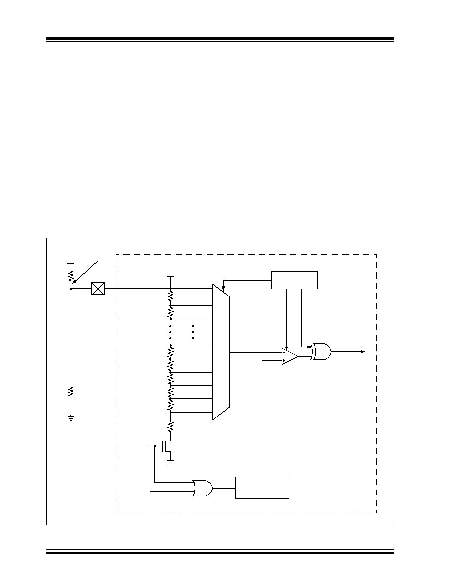
PIC18F2450/4450
DS39760A-page 184
Advance Information
� 2006 Microchip Technology Inc.
The module is enabled by setting the HLVDEN bit.
Each time that the HLVD module is enabled, the
circuitry requires some time to stabilize. The IRVST bit
is a read-only bit and is used to indicate when the circuit
is stable. The module can only generate an interrupt
after the circuit is stable and IRVST is set.
The VDIRMAG bit determines the overall operation of
the module. When VDIRMAG is cleared, the module
monitors for drops in V
DD
below a predetermined set
point. When the bit is set, the module monitors for rises
in V
DD
above the set point.
17.1
Operation
When the HLVD module is enabled, a comparator uses
an internally generated reference voltage as the set
point. The set point is compared with the trip point,
where each node in the resistor divider represents a
trip point voltage. The "trip point" voltage is the voltage
level at which the device detects a high or low-voltage
event, depending on the configuration of the module.
When the supply voltage is equal to the trip point, the
voltage tapped off of the resistor array is equal to the
internal reference voltage generated by the voltage
reference module. The comparator then generates an
interrupt signal by setting the HLVDIF bit.
The trip point voltage is software programmable to any
one of 16 values. The trip point is selected by
programming the HLVDL3:HLVDL0 bits
(HLVDCON<3:0>).
The HLVD module has an additional feature that allows
the user to supply the trip voltage to the module from an
external source. This mode is enabled when bits,
HLVDL3:HLVDL0, are set to `1111'. In this state, the
comparator input is multiplexed from the external input
pin, HLVDIN. This gives users flexibility because it
allows them to configure the High/Low-Voltage Detect
interrupt to occur at any voltage in the valid operating
range.
FIGURE 17-1:
HLVD MODULE BLOCK DIAGRAM (WITH EXTERNAL INPUT)
Set
V
DD
16-to
-1 MUX
HLVDEN
HLVDCON
HLVDL3:HLVDL0
Register
HLVDIN
V
DD
Externally Generated
Trip Point
HLVDIF
HLVDEN
BOREN
Internal Voltage
Reference
VDIRMAG
1.2V Typical
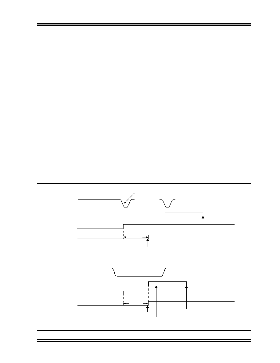
PIC18F2450/4450
� 2006 Microchip Technology Inc.
Advance Information
DS39760A-page 185
17.2
HLVD Setup
The following steps are needed to set up the HLVD
module:
1.
Disable the module by clearing the HLVDEN bit
(HLVDCON<4>).
2.
Write the value to the HLVDL3:HLVDL0 bits that
selects the desired HLVD trip point.
3.
Set the VDIRMAG bit to detect high voltage
(VDIRMAG = 1) or low voltage (VDIRMAG = 0).
4.
Enable the HLVD module by setting the
HLVDEN bit.
5.
Clear the HLVD Interrupt Flag, HLVDIF
(PIR2<2>), which may have been set from a
previous interrupt.
6.
Enable the HLVD interrupt, if interrupts are
desired, by setting the HLVDIE and GIE/GIEH
bits (PIE2<2> and INTCON<7>). An interrupt
will not be generated until the IRVST bit is set.
17.3
Current Consumption
When the module is enabled, the HLVD comparator
and voltage divider are enabled and will consume static
current. The total current consumption, when enabled,
is specified in electrical specification parameter D022
(Section 268 "DC Characteristics").
Depending on the application, the HLVD module does
not need to be operating constantly. To decrease the
current requirements, the HLVD circuitry may only
need to be enabled for short periods where the voltage
is checked. After doing the check, the HLVD module
may be disabled.
17.4
HLVD Start-up Time
The internal reference voltage of the HLVD module,
specified in electrical specification parameter D420 (see
Table 21-4 in Section 21.0 "Electrical Characteris-
tics"), may be used by other internal circuitry, such as
the Programmable Brown-out Reset. If the HLVD or
other circuits using the voltage reference are disabled to
lower the device's current consumption, the reference
voltage circuit will require time to become stable before
a low or high-voltage condition can be reliably detected.
This start-up time, T
IRVST
, is an interval that is
independent of device clock speed. It is specified in
electrical specification parameter 36 (Table 21-10).
The HLVD interrupt flag is not enabled until T
IRVST
has
expired and a stable reference voltage is reached. For
this reason, brief excursions beyond the set point may
not be detected during this interval. Refer to Figure 17-2
or Figure 17-3.
FIGURE 17-2:
LOW-VOLTAGE DETECT OPERATION (VDIRMAG =
0
)
V
HLVD
V
DD
HLVDIF
V
HLVD
V
DD
Enable HLVD
T
IRVST
HLVDIF may not be set
Enable HLVD
HLVDIF
HLVDIF cleared in software
HLVDIF cleared in software
HLVDIF cleared in software,
CASE 1:
CASE 2:
HLVDIF remains set since HLVD condition still exists
T
IRVST
Internal Reference is stable
Internal Reference is stable
IRVST
IRVST
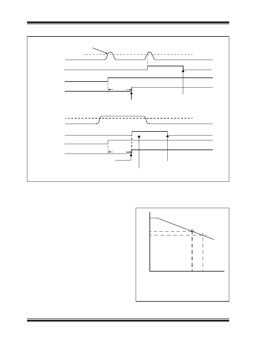
PIC18F2450/4450
DS39760A-page 186
Advance Information
� 2006 Microchip Technology Inc.
FIGURE 17-3:
HIGH-VOLTAGE DETECT OPERATION (VDIRMAG =
1
)
17.5
Applications
In many applications, the ability to detect a drop below
or rise above a particular threshold is desirable. For
example, the HLVD module could be periodically
enabled to detect Universal Serial Bus (USB) attach or
detach. This assumes the device is powered by a lower
voltage source than the USB when detached. An attach
would indicate a high-voltage detect from, for example,
3.3V to 5V (the voltage on USB) and vice versa for a
detach. This feature could save a design a few extra
components and an attach signal (input pin).
For general battery applications, Figure 17-4 shows a
possible voltage curve. Over time, the device voltage
decreases. When the device voltage reaches voltage,
V
A
, the HLVD logic generates an interrupt at time, T
A
.
The interrupt could cause the execution of an ISR,
which would allow the application to perform "house-
keeping tasks" and perform a controlled shutdown
before the device voltage exits the valid operating
range at T
B
. The HLVD, thus, would give the applica-
tion a time window, represented by the difference
between T
A
and T
B
, to safely exit.
FIGURE 17-4:
TYPICAL
HIGH/LOW-VOLTAGE
DETECT APPLICATION
V
HLVD
V
DD
HLVDIF
V
HLVD
V
DD
Enable HLVD
T
IRVST
HLVDIF may not be set
Enable HLVD
HLVDIF
HLVDIF cleared in software
HLVDIF cleared in software
HLVDIF cleared in software,
CASE 1:
CASE 2:
HLVDIF remains set since HLVD condition still exists
T
IRVST
IRVST
Internal Reference is stable
Internal Reference is stable
IRVST
Time
Vo
l
t
a
g
e
V
A
V
B
T
A
T
B
V
A
= HLVD trip point
V
B
= Minimum valid device
operating voltage
Legend:
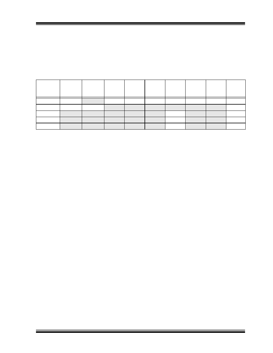
PIC18F2450/4450
� 2006 Microchip Technology Inc.
Advance Information
DS39760A-page 187
17.6
Operation During Sleep
When enabled, the HLVD circuitry continues to operate
during Sleep. If the device voltage crosses the trip
point, the HLVDIF bit will be set and the device will
wake-up from Sleep. Device execution will continue
from the interrupt vector address if interrupts have
been globally enabled.
17.7
Effects of a Reset
A device Reset forces all registers to their Reset state.
This forces the HLVD module to be turned off.
TABLE 17-1:
REGISTERS ASSOCIATED WITH HIGH/LOW-VOLTAGE DETECT MODULE
Name
Bit 7
Bit 6
Bit 5
Bit 4
Bit 3
Bit 2
Bit 1
Bit 0
Reset
Values
on page
HLVDCON
VDIRMAG
--
IRVST
HLVDEN
HLVDL3
HLVDL2
HLVDL1
HLVDL0
50
INTCON
GIE/GIEH PEIE/GIEL
TMR0IE
INT0IE
RBIE
TMR0IF
INT0IF
RBIF
49
PIR2
OSCFIF
--
USBIF
--
--
HLVDIF
--
--
51
PIE2
OSCFIE
--
USBIE
--
--
HLVDIE
--
--
51
IPR2
OSCFIP
--
USBIP
--
--
HLVDIP
--
--
51
Legend: -- = unimplemented, read as `0'. Shaded cells are unused by the HLVD module.

PIC18F2450/4450
DS39760A-page 188
Advance Information
� 2006 Microchip Technology Inc.
NOTES:

PIC18F2450/4450
� 2006 Microchip Technology Inc.
Advance Information
DS39760A-page 189
18.0
SPECIAL FEATURES OF THE
CPU
PIC18F2450/4450 devices include several features
intended to maximize reliability and minimize cost
through elimination of external components. These are:
� Oscillator Selection
� Resets:
- Power-on Reset (POR)
- Power-up Timer (PWRT)
- Oscillator Start-up Timer (OST)
- Brown-out Reset (BOR)
� Interrupts
� Watchdog Timer (WDT)
� Fail-Safe Clock Monitor
� Two-Speed Start-up
� Code Protection
� ID Locations
� In-Circuit Serial Programming
The oscillator can be configured for the application
depending on frequency, power, accuracy and cost. All
of the options are discussed in detail in Section 2.0
"Oscillator Configurations".
A complete discussion of device Resets and interrupts
is available in previous sections of this data sheet.
In addition to their Power-up and Oscillator Start-up
Timers provided for Resets, PIC18F2450/4450 devices
have a Watchdog Timer, which is either permanently
enabled via the Configuration bits or software controlled
(if configured as disabled).
The inclusion of an internal RC oscillator also provides
the additional benefits of a Fail-Safe Clock Monitor
(FSCM) and Two-Speed Start-up. FSCM provides for
background monitoring of the peripheral clock and
automatic switchover in the event of its failure. Two-
Speed Start-up enables code to be executed almost
immediately on start-up, while the primary clock source
completes its start-up delays.
All of these features are enabled and configured by
setting the appropriate Configuration register bits.

PIC18F2450/4450
DS39760A-page 190
Advance Information
� 2006 Microchip Technology Inc.
18.1
Configuration Bits
The Configuration bits can be programmed (read as
`0') or left unprogrammed (read as `1') to select various
device configurations. These bits are mapped starting
at program memory location 300000h.
The user will note that address 300000h is beyond the
user program memory space. In fact, it belongs to the
configuration memory space (300000h-3FFFFFh), which
can only be accessed using table reads and table writes.
Programming the Configuration registers is done in a
manner similar to programming the Flash memory. The
WR bit in the EECON1 register starts a self-timed write
to the Configuration register. In normal operation mode,
a TBLWT instruction, with the TBLPTR pointing to the
Configuration register, sets up the address and the
data for the Configuration register write. Setting the WR
bit starts a long
write to the Configuration register. The
Configuration registers are written a byte at a time. To
write or erase a configuration cell, a TBLWT instruction
can write a `1' or a `0' into the cell. For additional details
on Flash programming, refer to Section 6.5 "Writing
to Flash Program Memory".
TABLE 18-1:
CONFIGURATION BITS AND DEVICE IDs
File Name
Bit 7
Bit 6
Bit 5
Bit 4
Bit 3
Bit 2
Bit 1
Bit 0
Default/
Unprogrammed
Value
300000h
CONFIG1L
--
--
USBDIV CPUDIV1 CPUDIV0
PLLDIV2
PLLDIV1
PLLDIV0
--00 0000
300001h
CONFIG1H
IESO
FCMEN
--
--
FOSC3
FOSC2
FOSC1
FOSC0
00-- 0101
300002h
CONFIG2L
--
--
VREGEN
BORV1
BORV0
BOREN1
BOREN0 PWRTEN
--01 1111
300003h
CONFIG2H
--
--
--
WDTPS3
WDTPS2
WDTPS1
WDTPS0
WDTEN
---1 1111
300005h
CONFIG3H
MCLRE
--
--
--
--
LPT1OSC PBADEN
--
1--- -01-
300006h
CONFIG4L
DEBUG
XINST
ICPRT
(2)
--
BBSIZ
LVP
--
STVREN
100- 01-1
300008h
CONFIG5L
--
--
--
--
--
--
CP1
CP0
---- --11
300009h
CONFIG5H
--
CPB
--
--
--
--
--
--
-1-- ----
30000Ah
CONFIG6L
--
--
--
--
--
--
WRT1
WRT0
---- --11
30000Bh
CONFIG6H
--
WRTB
WRTC
--
--
--
--
--
-11- ----
30000Ch
CONFIG7L
--
--
--
--
--
--
EBTR1
EBTR0
---- --11
30000Dh
CONFIG7H
--
EBTRB
--
--
--
--
--
--
-1-- ----
3FFFFEh
DEVID1
DEV2
DEV1
DEV0
REV4
REV3
REV2
REV1
REV0
xxxx xxxx
(1)
3FFFFFh
DEVID2
DEV10
DEV9
DEV8
DEV7
DEV6
DEV5
DEV4
DEV3
0001 0010
(1)
Legend:
x
= unknown, u = unchanged, - = unimplemented. Shaded cells are unimplemented, read as `0'.
Note
1:
See Register 18-13 and Register 18-14 for device ID values. DEVID registers are read-only and cannot be programmed
by the user.
2:
Available only on PIC18F4450 devices in 44-pin TQFP packages. Always leave this bit clear in all other devices.

PIC18F2450/4450
� 2006 Microchip Technology Inc.
Advance Information
DS39760A-page 191
REGISTER 18-1:
CONFIG1L: CONFIGURATION REGISTER 1 LOW (BYTE ADDRESS 300000h)
U-0
U-0
R/P-0
R/P-0
R/P-0
R/P-1
R/P-1
R/P-1
--
--
USBDIV
CPUDIV1
CPUDIV0
PLLDIV2
PLLDIV1
PLLDIV0
bit 7
bit 0
Legend:
R = Readable bit
P = Programmable bit
U = Unimplemented bit, read as `0'
-n = Value when device is unprogrammed
u = Unchanged from programmed state
bit 7-6
Unimplemented: Read as `0'
bit 5
USBDIV: USB Clock Selection bit (used in Full-Speed USB mode only; UCFG:FSEN = 1)
1
= USB clock source comes from the 96 MHz PLL divided by 2
0
= USB clock source comes directly from the primary oscillator block with no postscale
bit 4-3
CPUDIV1:CPUDIV0: System Clock Postscaler Selection bits
For XT, HS, EC and ECIO Oscillator modes:
11
= Primary oscillator divided by 4 to derive system clock
10
= Primary oscillator divided by 3 to derive system clock
01
= Primary oscillator divided by 2 to derive system clock
00
= Primary oscillator used directly for system clock (no postscaler)
For XTPLL, HSPLL, ECPLL and ECPIO Oscillator modes:
11
= 96 MHz PLL divided by 6 to derive system clock
10
= 96 MHz PLL divided by 4 to derive system clock
01
= 96 MHz PLL divided by 3 to derive system clock
00
= 96 MHz PLL divided by 2 to derive system clock
bit 2-0
PLLDIV2:PLLDIV0: PLL Prescaler Selection bits
111
= Divide by 12 (48 MHz oscillator input)
110
= Divide by 10 (40 MHz oscillator input)
101
= Divide by 6 (24 MHz oscillator input)
100
= Divide by 5 (20 MHz oscillator input)
011
= Divide by 4 (16 MHz oscillator input)
010
= Divide by 3 (12 MHz oscillator input)
001
= Divide by 2 (8 MHz oscillator input)
000
= No prescale (4 MHz oscillator input drives PLL directly)

PIC18F2450/4450
DS39760A-page 192
Advance Information
� 2006 Microchip Technology Inc.
REGISTER 18-2:
CONFIG1H: CONFIGURATION REGISTER 1 HIGH (BYTE ADDRESS 300001h)
R/P-0
R/P-0
U-0
U-0
R/P-0
R/P-1
R/P-1
R/P-1
IESO
FCMEN
--
--
FOSC3
(1)
FOSC2
(1)
FOSC1
(1)
FOSC0
(1)
bit 7
bit 0
Legend:
R = Readable bit
P = Programmable bit
U = Unimplemented bit, read as `0'
-n = Value when device is unprogrammed
u = Unchanged from programmed state
bit 7
IESO: Internal/External Oscillator Switchover bit
1
= Oscillator Switchover mode enabled
0
= Oscillator Switchover mode disabled
bit 6
FCMEN: Fail-Safe Clock Monitor Enable bit
1
= Fail-Safe Clock Monitor enabled
0
= Fail-Safe Clock Monitor disabled
bit 5-4
Unimplemented: Read as `0'
bit 3-0
FOSC3:FOSC0: Oscillator Selection bits
(1)
111x
= HS oscillator, PLL enabled (HSPLL)
110x
= HS oscillator (HS)
1011
= Internal oscillator, HS oscillator used by USB (INTHS)
1010
= Internal oscillator, XT used by USB (INTXT)
1001
= Internal oscillator, CLKO function on RA6, EC used by USB (INTCKO)
1000
= Internal oscillator, port function on RA6, EC used by USB (INTIO)
0111
= EC oscillator, PLL enabled, CLKO function on RA6 (ECPLL)
0110
= EC oscillator, PLL enabled, port function on RA6 (ECPIO)
0101
= EC oscillator, CLKO function on RA6 (EC)
0100
= EC oscillator, port function on RA6 (ECIO)
001x
= XT oscillator, PLL enabled (XTPLL)
000x
= XT oscillator (XT)
Note 1:
The microcontroller and USB module both use the selected oscillator as their clock source in XT, HS and
EC modes. The USB module uses the indicated XT, HS or EC oscillator as its clock source whenever the
microcontroller uses the internal oscillator.

PIC18F2450/4450
� 2006 Microchip Technology Inc.
Advance Information
DS39760A-page 193
REGISTER 18-3:
CONFIG2L: CONFIGURATION REGISTER 2 LOW (BYTE ADDRESS 300002h)
U-0
U-0
R/P-0
R/P-1
R/P-1
R/P-1
R/P-1
R/P-1
--
--
VREGEN
BORV1
(1)
BORV0
(1)
BOREN1
(2)
BOREN0
(2)
PWRTEN
(2)
bit 7
bit 0
Legend:
R = Readable bit
P = Programmable bit
U = Unimplemented bit, read as `0'
-n = Value when device is unprogrammed
u = Unchanged from programmed state
bit 7-6
Unimplemented: Read as `0'
bit 5
VREGEN: USB Internal Voltage Regulator Enable bit
1
= USB voltage regulator enabled
0
= USB voltage regulator disabled
bit 4-3
BORV1:BORV0: Brown-out Reset Voltage bits
(1)
11
= Minimum setting
.
.
.
00
= Maximum setting
bit 2-1
BOREN1:BOREN0: Brown-out Reset Enable bits
(2)
11
= Brown-out Reset enabled in hardware only (SBOREN is disabled)
10
= Brown-out Reset enabled in hardware only and disabled in Sleep mode (SBOREN is disabled)
01
= Brown-out Reset enabled and controlled by software (SBOREN is enabled)
00
= Brown-out Reset disabled in hardware and software
bit 0
PWRTEN: Power-up Timer Enable bit
(2)
1
= PWRT disabled
0
= PWRT enabled
Note 1:
See Section 21.0 "Electrical Characteristics" for the specifications.
2:
The Power-up Timer is decoupled from Brown-out Reset, allowing these features to be independently
controlled.

PIC18F2450/4450
DS39760A-page 194
Advance Information
� 2006 Microchip Technology Inc.
REGISTER 18-4:
CONFIG2H: CONFIGURATION REGISTER 2 HIGH (BYTE ADDRESS 300003h)
U-0
U-0
U-0
R/P-1
R/P-1
R/P-1
R/P-1
R/P-1
--
--
--
WDTPS3
WDTPS2
WDTPS1
WDTPS0
WDTEN
bit 7
bit 0
Legend:
R = Readable bit
P = Programmable bit
U = Unimplemented bit, read as `0'
-n = Value when device is unprogrammed
u = Unchanged from programmed state
bit 7-5
Unimplemented: Read as `0'
bit 4-1
WDTPS3:WDTPS0: Watchdog Timer Postscale Select bits
1111
= 1:32,768
1110
= 1:16,384
1101
= 1:8,192
1100
= 1:4,096
1011
= 1:2,048
1010
= 1:1,024
1001
= 1:512
1000
= 1:256
0111
= 1:128
0110
= 1:64
0101
= 1:32
0100
= 1:16
0011
= 1:8
0010
= 1:4
0001
= 1:2
0000
= 1:1
bit 0
WDTEN: Watchdog Timer Enable bit
1
= WDT enabled
0
= WDT disabled (control is placed on the SWDTEN bit)

PIC18F2450/4450
� 2006 Microchip Technology Inc.
Advance Information
DS39760A-page 195
REGISTER 18-5:
CONFIG3H: CONFIGURATION REGISTER 3 HIGH (BYTE ADDRESS 300005h)
R/P-1
U-0
U-0
U-0
U-0
R/P-0
R/P-1
U-0
MCLRE
--
--
--
--
LPT1OSC
PBADEN
--
bit 7
bit 0
Legend:
R = Readable bit
P = Programmable bit
U = Unimplemented bit, read as `0'
-n = Value when device is unprogrammed
u = Unchanged from programmed state
bit 7
MCLRE: MCLR Pin Enable bit
1
= MCLR pin enabled, RA5 input pin disabled
0
= RA5 input pin enabled, MCLR pin disabled
bit 6-3
Unimplemented: Read as `0'
bit 2
LPT1OSC: Low-Power Timer1 Oscillator Enable bit
1
= Timer1 configured for low-power operation
0
= Timer1 configured for higher power operation
bit 1
PBADEN: PORTB A/D Enable bit
(Affects ADCON1 Reset state. ADCON1 controls PORTB<4:0> pin configuration.)
1
= PORTB<4:0> pins are configured as analog input channels on Reset
0
= PORTB<4:0> pins are configured as digital I/O on Reset
bit 0
Unimplemented: Read as `0'

PIC18F2450/4450
DS39760A-page 196
Advance Information
� 2006 Microchip Technology Inc.
REGISTER 18-6:
CONFIG4L: CONFIGURATION REGISTER 4 LOW (BYTE ADDRESS 300006h)
R/P-1
R/P-0
R/P-0
U-0
R/P-0
R/P-1
U-0
R/P-1
DEBUG
XINST
ICPRT
(1)
--
BBSIZ
LVP
--
STVREN
bit 7
bit 0
Legend:
R = Readable bit
P = Programmable bit
U = Unimplemented bit, read as `0'
-n = Value when device is unprogrammed
u = Unchanged from programmed state
bit 7
DEBUG: Background Debugger Enable bit
1
= Background debugger disabled, RB6 and RB7 configured as general purpose I/O pins
0
= Background debugger enabled, RB6 and RB7 are dedicated to In-Circuit Debug
bit 6
XINST: Extended Instruction Set Enable bit
1
= Instruction set extension and Indexed Addressing mode enabled
0
= Instruction set extension and Indexed Addressing mode disabled (Legacy mode)
bit 5
ICPRT: Dedicated In-Circuit Debug/Programming Port (ICPORT) Enable bit
(1)
1
= ICPORT enabled
0
= ICPORT disabled
bit 4
Unimplemented: Read as `0'
bit 3
BBSIZ: Boot Block Size Select bit
1
= 2 kW Boot Block size
0
= 1 kW Boot Block size
bit 2
LVP: Single-Supply ICSPTM Enable bit
1
= Single-Supply ICSP enabled
0
= Single-Supply ICSP disabled
bit 1
Unimplemented: Read as `0'
bit 0
STVREN: Stack Full/Underflow Reset Enable bit
1
= Stack full/underflow will cause Reset
0
= Stack full/underflow will not cause Reset
Note 1:
Available only on PIC18F4450 devices in 44-pin TQFP packages. Always leave this bit clear in all other
devices.
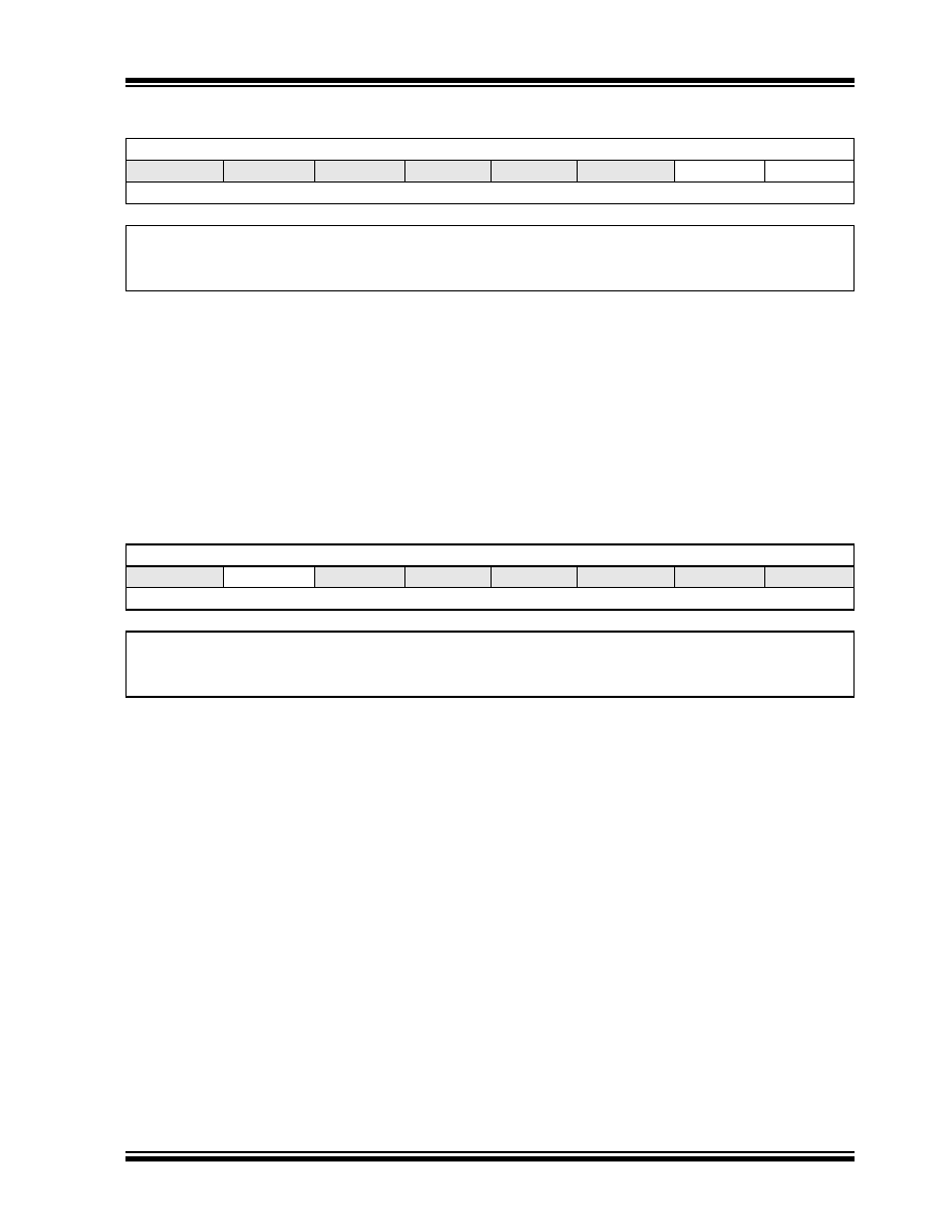
PIC18F2450/4450
� 2006 Microchip Technology Inc.
Advance Information
DS39760A-page 197
REGISTER 18-7:
CONFIG5L: CONFIGURATION REGISTER 5 LOW (BYTE ADDRESS 300008h)
U-0
U-0
U-0
U-0
U-0
U-0
R/C-1
R/C-1
--
--
--
--
--
--
CP1
CP0
bit 7
bit 0
Legend:
R = Readable bit
C = Clearable bit
U = Unimplemented bit, read as `0'
-n = Value when device is unprogrammed
u = Unchanged from programmed state
bit 7-2
Unimplemented: Read as `0'
bit 1
CP1: Code Protection bit
1
= Block 1 (002000-003FFFh) is not code-protected
0
= Block 1 (002000-003FFFh) is code-protected
bit 0
CP0: Code Protection bit
1
= Block 0 (000800-001FFFh) or (001000-001FFFh) is not code-protected
0
= Block 0 (000800-001FFFh) or (001000-001FFFh) is code-protected
REGISTER 18-8:
CONFIG5H: CONFIGURATION REGISTER 5 HIGH (BYTE ADDRESS 300009h)
U-0
R/C-1
U-0
U-0
U-0
U-0
U-0
U-0
--
CPB
--
--
--
--
--
--
bit 7
bit 0
Legend:
R = Readable bit
C = Clearable bit
U = Unimplemented bit, read as `0'
-n = Value when device is unprogrammed
u = Unchanged from programmed state
bit 7
Unimplemented: Read as `0'
bit 6
CPB: Boot Block Code Protection bit
1
= Boot block (000000-0007FFh) or (000000-000FFFh) is not code-protected
0
= Boot block (000000-0007FFh) or (000000-000FFFh) is code-protected
bit 5-0
Unimplemented: Read as `0'
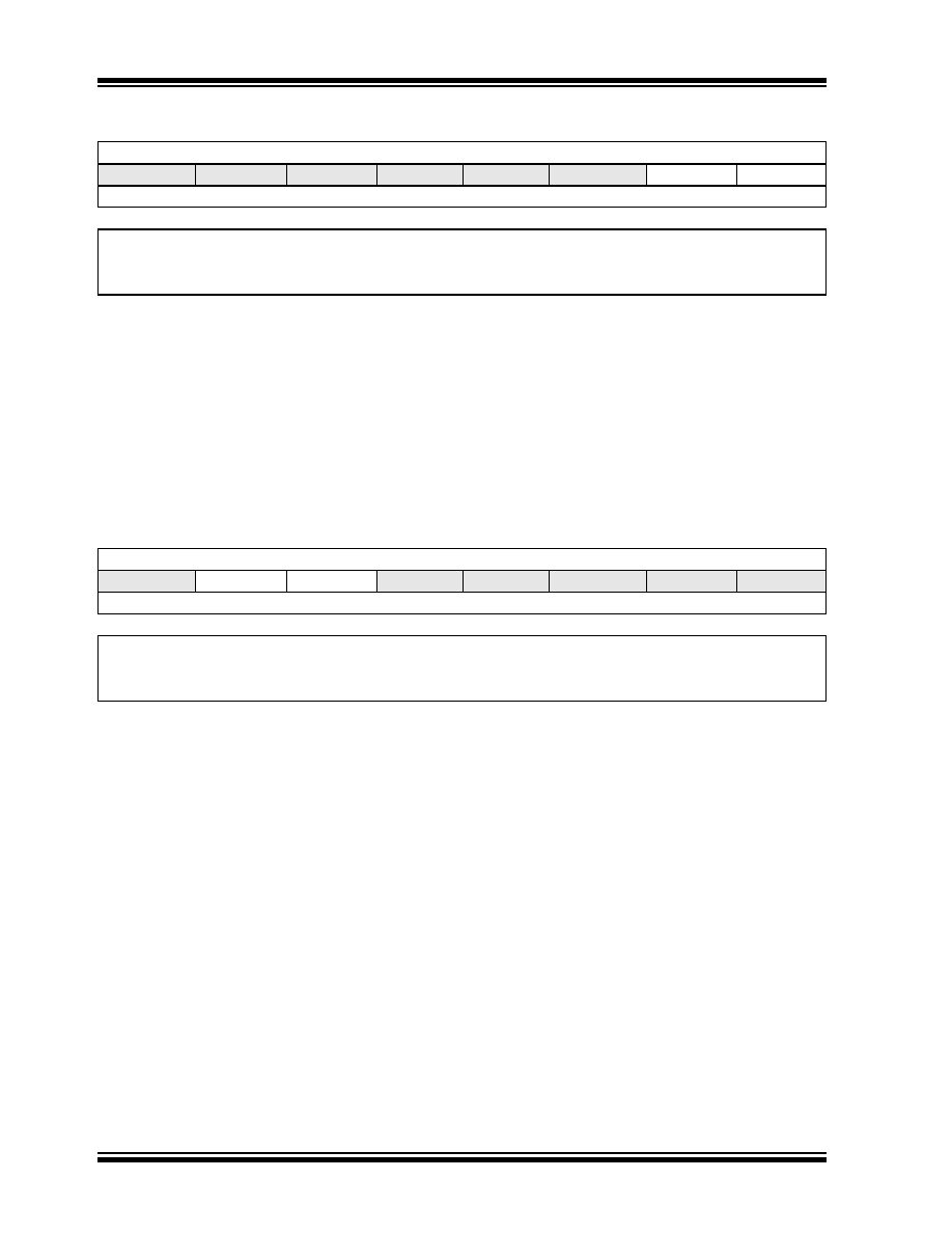
PIC18F2450/4450
DS39760A-page 198
Advance Information
� 2006 Microchip Technology Inc.
REGISTER 18-9:
CONFIG6L: CONFIGURATION REGISTER 6 LOW (BYTE ADDRESS 30000Ah)
U-0
U-0
U-0
U-0
U-0
U-0
R/C-1
R/C-1
--
--
--
--
--
--
WRT1
WRT0
bit 7
bit 0
Legend:
R = Readable bit
C = Clearable bit
U = Unimplemented bit, read as `0'
-n = Value when device is unprogrammed
u = Unchanged from programmed state
bit 7-2
Unimplemented: Read as `0'
bit 1
WRT1: Write Protection bit
1
= Block 1 (002000-003FFFh) is not write-protected
0
= Block 1 (002000-003FFFh) is write-protected
bit 0
WRT0: Write Protection bit
1
= Block 0 (000800-001FFFh) or (001000-001FFFh) is not write-protected
0
= Block 0 (000800-001FFFh) or (001000-001FFFh) is write-protected
REGISTER 18-10: CONFIG6H: CONFIGURATION REGISTER 6 HIGH (BYTE ADDRESS 30000Bh)
U-0
R/C-1
R-1
U-0
U-0
U-0
U-0
U-0
--
WRTB
WRTC
(1)
--
--
--
--
--
bit 7
bit 0
Legend:
R = Readable bit
C = Clearable bit
U = Unimplemented bit, read as `0'
-n = Value when device is unprogrammed
u = Unchanged from programmed state
bit 7
Unimplemented: Read as `0'
bit 6
WRTB: Boot Block Write Protection bit
1
= Boot block (000000-0007FFh) or (000000-000FFFh) is not write-protected
0
= Boot block (000000-0007FFh) or (000000-000FFFh) is write-protected
bit 5
WRTC: Configuration Register Write Protection bit
(1)
1
= Configuration registers (300000-3000FFh) are not write-protected
0
= Configuration registers (300000-3000FFh) are write-protected
bit 4-0
Unimplemented: Read as `0'
Note 1:
This bit is read-only in normal execution mode; it can be written only in Program mode.
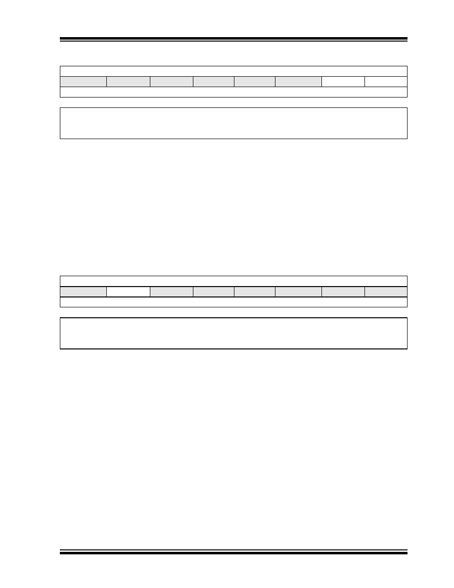
PIC18F2450/4450
� 2006 Microchip Technology Inc.
Advance Information
DS39760A-page 199
REGISTER 18-11: CONFIG7L: CONFIGURATION REGISTER 7 LOW (BYTE ADDRESS 30000Ch)
U-0
U-0
U-0
U-0
U-0
U-0
R/C-1
R/C-1
--
--
--
--
--
--
EBTR1
EBTR0
bit 7
bit 0
Legend:
R = Readable bit
C = Clearable bit
U = Unimplemented bit, read as `0'
-n = Value when device is unprogrammed
u = Unchanged from programmed state
bit 7-2
Unimplemented: Read as `0'
bit 1
EBTR1: Table Read Protection bit
1
= Block 1 (002000-003FFFh) is not protected from table reads executed in other blocks
0
= Block 1 (002000-003FFFh) is protected from table reads executed in other blocks
bit 0
EBTR0: Table Read Protection bit
1
= Block 0 (000800-001FFFh) or (001000-001FFFh) is not protected from table reads executed in
other blocks
0
= Block 0 (000800-001FFFh) or (001000-001FFFh) is protected from table reads executed in other
blocks
REGISTER 18-12: CONFIG7H: CONFIGURATION REGISTER 7 HIGH (BYTE ADDRESS 30000Dh)
U-0
R/C-1
U-0
U-0
U-0
U-0
U-0
U-0
--
EBTRB
--
--
--
--
--
--
bit 7
bit 0
Legend:
R = Readable bit
C = Clearable bit
U = Unimplemented bit, read as `0'
-n = Value when device is unprogrammed
u = Unchanged from programmed state
bit 7
Unimplemented: Read as `0'
bit 6
EBTRB: Boot Block Table Read Protection bit
1
= Boot block (000000-0007FFh) or (000000-000FFFh) is not protected from table reads executed
in other blocks
0
= Boot block (000000-0007FFh) or (000000-000FFFh) is protected from table reads executed in
other blocks
bit 5-0
Unimplemented: Read as `0'
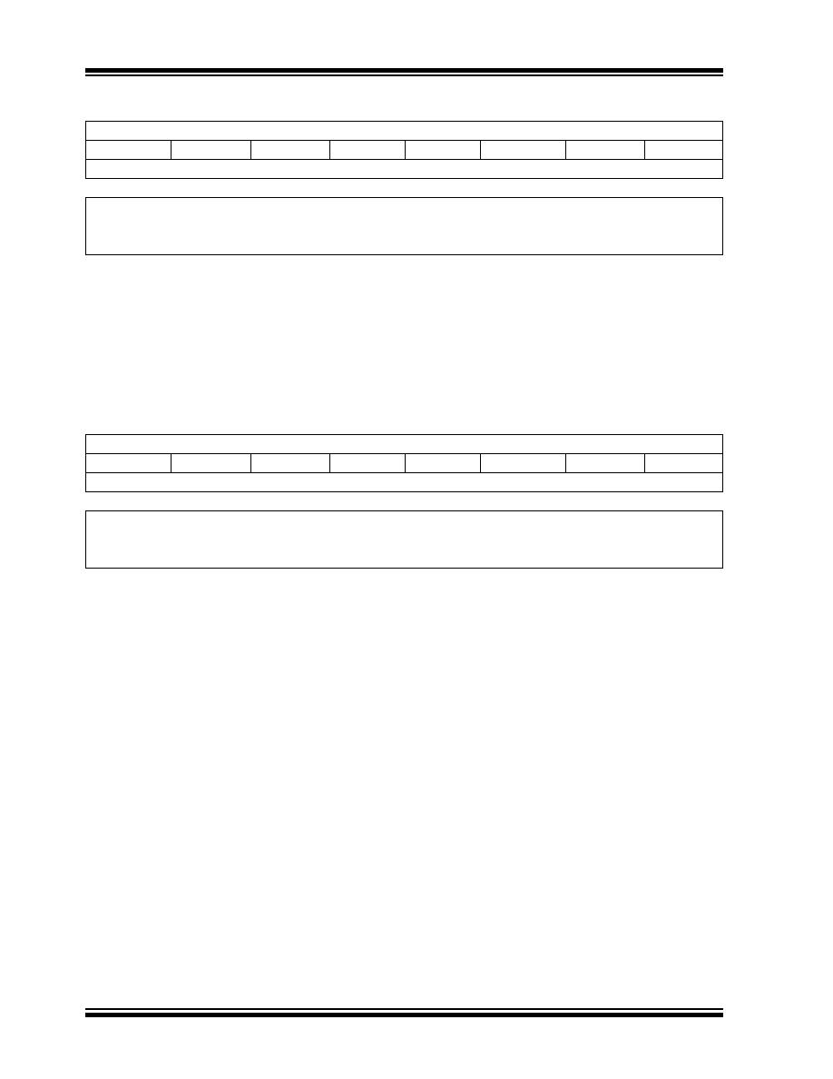
PIC18F2450/4450
DS39760A-page 200
Advance Information
� 2006 Microchip Technology Inc.
REGISTER 18-13: DEVID1: DEVICE ID REGISTER 1 FOR PIC18F2450/4450 DEVICES
R
R
R
R
R
R
R
R
DEV2
DEV1
DEV0
REV4
REV3
REV2
REV1
REV0
bit 7
bit 0
Legend:
R = Read-only bit
P = Programmable bit
U = Unimplemented bit, read as `0'
-n = Value when device is unprogrammed
u = Unchanged from programmed state
bit 7-5
DEV2:DEV0: Device ID bits
001
= PIC18F2450
000
= PIC18F4450
bit 4-0
REV3:REV0: Revision ID bits
These bits are used to indicate the device revision.
REGISTER 18-14: DEVID2: DEVICE ID REGISTER 2 FOR PIC18F2450/4450 DEVICES
R
R
R
R
R
R
R
R
DEV10
(1)
DEV9
(1)
DEV8
(1)
DEV7
(1)
DEV6
(1)
DEV5
(1)
DEV4
(1)
DEV3
(1)
bit 7
bit 0
Legend:
R = Read-only bit
P = Programmable bit
U = Unimplemented bit, read as `0'
-n = Value when device is unprogrammed
u = Unchanged from programmed state
bit 7-0
DEV10:DEV3: Device ID bits
(1)
These bits are used with the DEV2:DEV0 bits in the DEVID1 register to identify the part number.
0010 0100
= PIC18F2450/4450 devices
Note 1:
These values for DEV10:DEV3 may be shared with other devices. The specific device is always identified
by using the entire DEV10:DEV0 bit sequence.
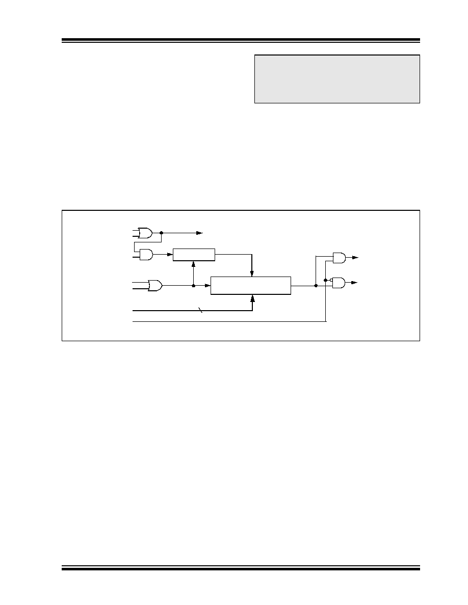
PIC18F2450/4450
� 2006 Microchip Technology Inc.
Advance Information
DS39760A-page 201
18.2
Watchdog Timer (WDT)
For PIC18F2450/4450 devices, the WDT is driven by
the INTRC source. When the WDT is enabled, the
clock source is also enabled. The nominal WDT period
is 4 ms and has the same stability as the INTRC
oscillator.
The 4 ms period of the WDT is multiplied by a 16-bit
postscaler. Any output of the WDT postscaler is
selected by a multiplexer, controlled by bits in
Configuration Register 2H. Available periods range
from 4 ms to 131.072 seconds (2.18 minutes). The
WDT and postscaler are cleared when any of the
following events occur: a SLEEP or CLRWDT instruction
is executed or a clock failure has occurred.
.
18.2.1
CONTROL REGISTER
Register 18-15 shows the WDTCON register. This is a
readable and writable register which contains a control
bit that allows software to override the WDT enable
Configuration bit, but only if the Configuration bit has
disabled the WDT.
FIGURE 18-1:
WDT BLOCK DIAGRAM
Note 1: The CLRWDT and SLEEP instructions
clear the WDT and postscaler counts
when executed.
2: When a CLRWDT instruction is executed,
the postscaler count will be cleared.
INTRC Source
WDT
Wake-up from
Reset
WDT
WDT Counter
Programmable Postscaler
1:1 to 1:32,768
Enable WDT
WDTPS<3:0>
SWDTEN
WDTEN
CLRWDT
4
Power-Managed
Reset
All Device Resets
SLEEP
INTRC Control
�128
Modes
PIC18F2450/4450
DS39760A-page 202
Advance Information
� 2006 Microchip Technology Inc.
TABLE 18-2:
SUMMARY OF WATCHDOG TIMER REGISTERS
REGISTER 18-15: WDTCON: WATCHDOG TIMER CONTROL REGISTER
U-0
U-0
U-0
U-0
U-0
U-0
U-0
R/W-0
--
--
--
--
--
--
--
SWDTEN
(1)
bit 7
bit 0
Legend:
R = Readable bit
W = Writable bit
U = Unimplemented bit, read as `0'
-n = Value at POR
`1' = Bit is set
`0' = Bit is cleared
x = Bit is unknown
bit 7-1
Unimplemented: Read as `0'
bit 0
SWDTEN: Software Controlled Watchdog Timer Enable bit
(1)
1
= Watchdog Timer is on
0
= Watchdog Timer is off
Note 1:
This bit has no effect if the Configuration bit, WDTEN, is enabled.
Name
Bit 7
Bit 6
Bit 5
Bit 4
Bit 3
Bit 2
Bit 1
Bit 0
Reset
Values
on page
RCON
IPEN
SBOREN
(1)
--
RI
TO
PD
POR
BOR
50
WDTCON
--
--
--
--
--
--
--
SWDTEN
50
Legend: -- = unimplemented, read as `0'. Shaded cells are not used by the Watchdog Timer.
Note 1:
The SBOREN bit is only available when BOREN<1:0> = 01; otherwise, the bit reads as `0'.
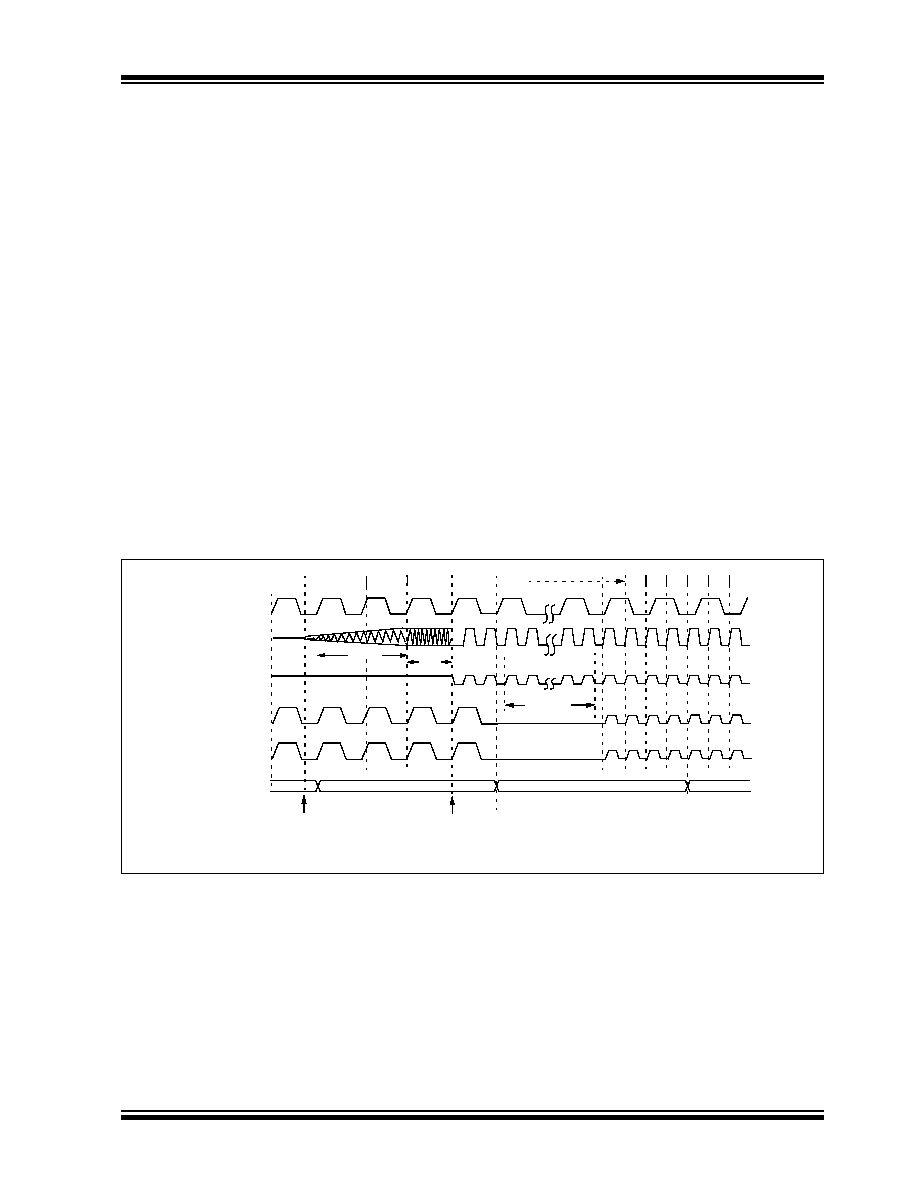
PIC18F2450/4450
� 2006 Microchip Technology Inc.
Advance Information
DS39760A-page 203
18.3
Two-Speed Start-up
The Two-Speed Start-up feature helps to minimize the
latency period, from oscillator start-up to code
execution, by allowing the microcontroller to use the
INTRC oscillator as a clock source until the primary
clock source is available. It is enabled by setting the
IESO Configuration bit.
Two-Speed Start-up should be enabled only if the
primary oscillator mode is XT, HS, XTPLL or HSPLL
(Crystal-based modes). Other sources do not require
an OST start-up delay; for these, Two-Speed Start-up
should be disabled.
When enabled, Resets and wake-ups from Sleep mode
cause the device to configure itself to run from the
internal oscillator as the clock source, following the
time-out of the Power-up Timer after a Power-on Reset
is enabled. This allows almost immediate code
execution while the primary oscillator starts and the
OST is running. Once the OST times out, the device
automatically switches to PRI_RUN mode.
Because the OSCCON register is cleared on Reset
events, the INTRC clock is used directly at its base
frequency.
In all other power-managed modes, Two-Speed Start-up
is not used. The device will be clocked by the currently
selected clock source until the primary clock source
becomes available. The setting of the IESO bit is
ignored.
18.3.1
SPECIAL CONSIDERATIONS FOR
USING TWO-SPEED START-UP
While using the INTRC oscillator in Two-Speed Start-up,
the device still obeys the normal command sequences
for entering power-managed modes, including serial
SLEEP
instructions (refer to Section 3.1.4 "Multiple
Sleep Commands"). In practice, this means that user
code can change the SCS1:SCS0 bit settings or issue
SLEEP
instructions before the OST times out. This would
allow an application to briefly wake-up, perform routine
"housekeeping" tasks and return to Sleep before the
device starts to operate from the primary oscillator.
User code can also check if the primary clock source is
currently providing the device clocking by checking the
status of the OSTS bit (OSCCON<3>). If the bit is set,
the primary oscillator is providing the clock. Otherwise,
the internal oscillator is providing the clock during
wake-up from Reset or Sleep mode.
FIGURE 18-2:
TIMING TRANSITION FOR TWO-SPEED START-UP (INTRC TO HSPLL)
Q1
Q3 Q4
OSC1
Peripheral
Program
PC
PC + 2
INTRC
PLL Clock
Q1
PC + 6
Q2
Output
Q3
Q4
Q1
CPU Clock
PC + 4
Clock
Counter
Q2
Q2
Q3
Note 1:
T
OST
= 1024 T
OSC
; T
PLL
= 2 ms (approx). These intervals are not shown to scale.
Wake from Interrupt Event
T
PLL
(1)
1
2
n-1
n
Clock
OSTS bit Set
Transition
T
OST
(1)
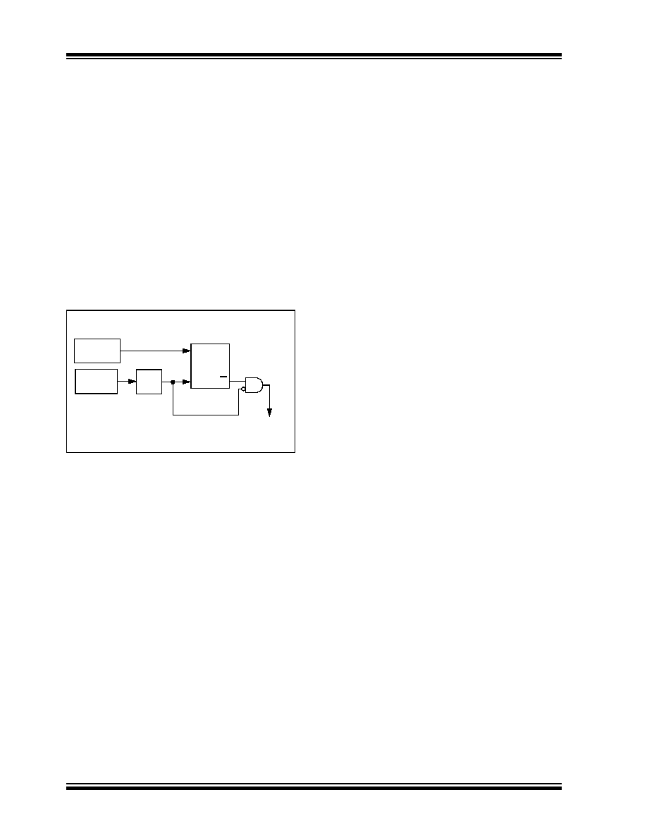
PIC18F2450/4450
DS39760A-page 204
Advance Information
� 2006 Microchip Technology Inc.
18.4
Fail-Safe Clock Monitor
The Fail-Safe Clock Monitor (FSCM) allows the
microcontroller to continue operation in the event of an
external oscillator failure by automatically switching the
device clock to the internal oscillator. The FSCM function
is enabled by setting the FCMEN Configuration bit.
When FSCM is enabled, the INTRC oscillator runs at all
times to monitor clocks to peripherals and provide a
backup clock in the event of a clock failure. Clock
monitoring (shown in Figure 18-3) is accomplished by
creating a sample clock signal, which is the INTRC output
divided by 64. This allows ample time between FSCM
sample clocks for a peripheral clock edge to occur. The
peripheral device clock and the sample clock are
presented as inputs to the Clock Monitor latch (CM). The
CM is set on the falling edge of the device clock source,
but cleared on the rising edge of the sample clock.
FIGURE 18-3:
FSCM BLOCK DIAGRAM
Clock failure is tested for on the falling edge of the
sample clock. If a sample clock falling edge occurs
while CM is still set, a clock failure has been detected
(Figure 18-4). This causes the following:
� the FSCM generates an oscillator fail interrupt by
setting bit, OSCFIF (PIR2<7>);
� the device clock source is switched to the internal
oscillator (OSCCON is not updated to show the cur-
rent clock source � this is the fail-safe condition); and
� the WDT is reset.
The FSCM will detect failures of the primary or
secondary clock sources only. If the internal oscillator
fails, no failure would be detected, nor would any action
be possible.
18.4.1
FSCM AND THE WATCHDOG TIMER
Both the FSCM and the WDT are clocked by the
INTRC oscillator. Since the WDT operates with a
separate divider and counter, disabling the WDT has
no effect on the operation of the INTRC oscillator when
the FSCM is enabled.
If the WDT is enabled with a small prescale value, a
decrease in clock speed allows a WDT time-out to
occur and a subsequent device Reset. For this reason,
Fail-Safe Clock Monitor events also reset the WDT and
postscaler, allowing it to start timing from when execu-
tion speed was changed and decreasing the likelihood
of an erroneous time-out.
18.4.2
EXITING FAIL-SAFE OPERATION
The fail-safe condition is terminated by either a device
Reset or by entering a power-managed mode. On
Reset, the controller starts the primary clock source
specified in Configuration Register 1H (with any start-
up delays that are required for the oscillator mode,
such as OST or PLL timer). The INTRC provides the
device clock until the primary clock source becomes
ready (similar to a Two-Speed Start-up). The clock
source is then switched to the primary clock (indicated
by the OSTS bit in the OSCCON register becoming
set). The Fail-Safe Clock Monitor then resumes
monitoring the peripheral clock.
The primary clock source may never become ready
during start-up. In this case, operation is clocked by the
INTRC. The OSCCON register will remain in its Reset
state until a power-managed mode is entered.
Peripheral
INTRC
� 64
S
C
Q
(32
s)
488 Hz
(2.048 ms)
Clock Monitor
Latch (CM)
(edge-triggered)
Clock
Failure
Detected
Source
Clock
Q
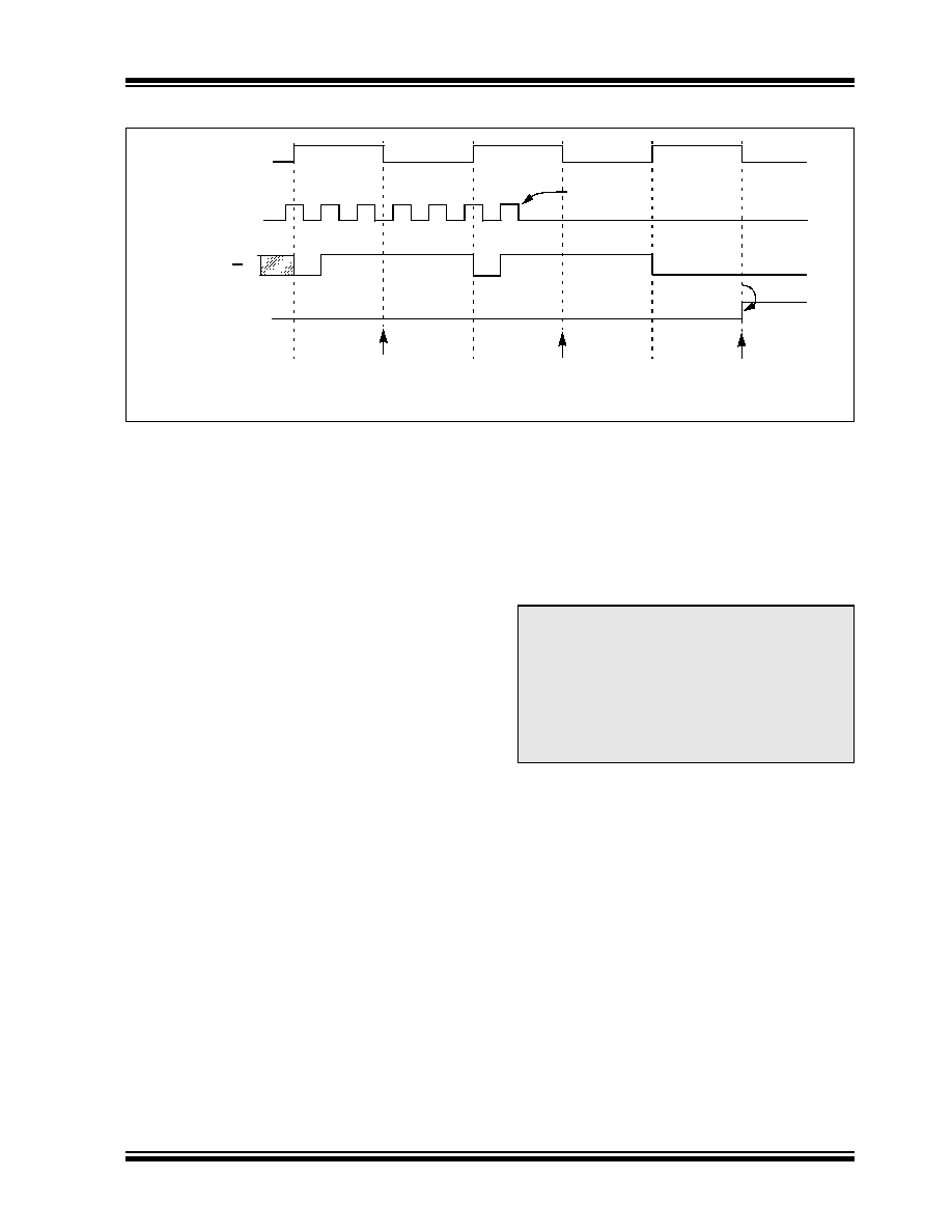
PIC18F2450/4450
� 2006 Microchip Technology Inc.
Advance Information
DS39760A-page 205
FIGURE 18-4:
FSCM TIMING DIAGRAM
18.4.3
FSCM INTERRUPTS IN
POWER-MANAGED MODES
By entering a power-managed mode, the clock multi-
plexer selects the clock source selected by the OSCCON
register. Fail-Safe Clock Monitoring of the power-
managed clock source resumes in the power-managed
mode.
If an oscillator failure occurs during power-managed
operation, the subsequent events depend on whether
or not the oscillator failure interrupt is enabled. If
enabled (OSCFIF = 1), code execution will be clocked
by the INTRC. An automatic transition back to the failed
clock source will not occur.
If the interrupt is disabled, subsequent interrupts while
in Idle mode will cause the CPU to begin executing
instructions while being clocked by the INTRC source.
18.4.4
POR OR WAKE-UP FROM SLEEP
The FSCM is designed to detect oscillator failure at any
point after the device has exited Power-on Reset
(POR) or Low-Power Sleep mode. When the primary
device clock is either EC or INTRC, monitoring can
begin immediately following these events.
For oscillator modes involving a crystal or resonator
(HS, HSPLL or XT), the situation is somewhat different.
Since the oscillator may require a start-up time
considerably longer than the FCSM sample clock time,
a false clock failure may be detected. To prevent this,
the internal oscillator is automatically configured as the
device clock and functions until the primary clock is
stable (the OST and PLL timers have timed out). This
is identical to Two-Speed Start-up mode. Once the
primary clock is stable, the INTRC returns to its role as
the FSCM source.
As noted in Section 18.3.1 "Special Considerations
for Using Two-Speed Start-up", it is also possible to
select another clock configuration and enter an alternate
power-managed mode while waiting for the primary
clock to become stable. When the new power-managed
mode is selected, the primary clock is disabled.
OSCFIF
CM Output
Device
Clock
Output
Sample Clock
Failure
Detected
Oscillator
Failure
Note:
The device clock is normally at a much higher frequency than the sample clock. The relative frequencies in this
example have been chosen for clarity.
(Q)
CM Test
CM Test
CM Test
Note:
The same logic that prevents false oscilla-
tor failure interrupts on POR or wake from
Sleep will also prevent the detection of the
oscillator's failure to start at all following
these events. This can be avoided by
monitoring the OSTS bit and using a
timing routine to determine if the oscillator
is taking too long to start. Even so, no
oscillator failure interrupt will be flagged.
PIC18F2450/4450
DS39760A-page 206
Advance Information
� 2006 Microchip Technology Inc.
18.5
Program Verification and
Code Protection
The overall structure of the code protection on the
PIC18 Flash devices differs significantly from other
PICmicro
�
devices.
The user program memory is divided into three blocks.
One of these is a boot block of 1 or 2 Kbytes. The
remainder of the memory is divided into two blocks on
binary boundaries.
Each of the three blocks has three code protection bits
associated with them. They are:
� Code-Protect bit (CPn)
� Write-Protect bit (WRTn)
� External Block Table Read bit (EBTRn)
Figure 18-5 shows the program memory organization
for 24 and 32-Kbyte devices and the specific code
protection bit associated with each block. The actual
locations of the bits are summarized in Table 18-3.
FIGURE 18-5:
CODE-PROTECTED PROGRAM MEMORY FOR PIC18F2450/4450
TABLE 18-3:
SUMMARY OF CODE PROTECTION REGISTERS
File Name
Bit 7
Bit 6
Bit 5
Bit 4
Bit 3
Bit 2
Bit 1
Bit 0
300008h
CONFIG5L
--
--
--
--
--
--
CP1
CP0
300009h
CONFIG5H
--
CPB
--
--
--
--
--
--
30000Ah
CONFIG6L
--
--
--
--
--
--
WRT1
WRT0
30000Bh
CONFIG6H
--
WRTB
WRTC
--
--
--
--
--
30000Ch
CONFIG7L
--
--
--
--
--
--
EBTR1
EBTR0
30000Dh
CONFIG7H
--
EBTRB
--
--
--
--
--
--
Legend: Shaded cells are unimplemented.
MEMORY SIZE/DEVICE
Block Code Protection
Controlled By:
16 Kbytes
(PIC18F2450/4450)
Address
Range
Boot Block
000000h
0007FFh
000FFFh
CPB, WRTB, EBTRB
Block 0
001000h
001FFFh
CP0, WRT0, EBTR0
Block 1
002000h
003FFFh
CP1, WRT1, EBTR1
Unimplemented
Read `0's
Unimplemented
Read `0's
Unimplemented
Read `0's
1FFFFFh
(Unimplemented Memory Space)
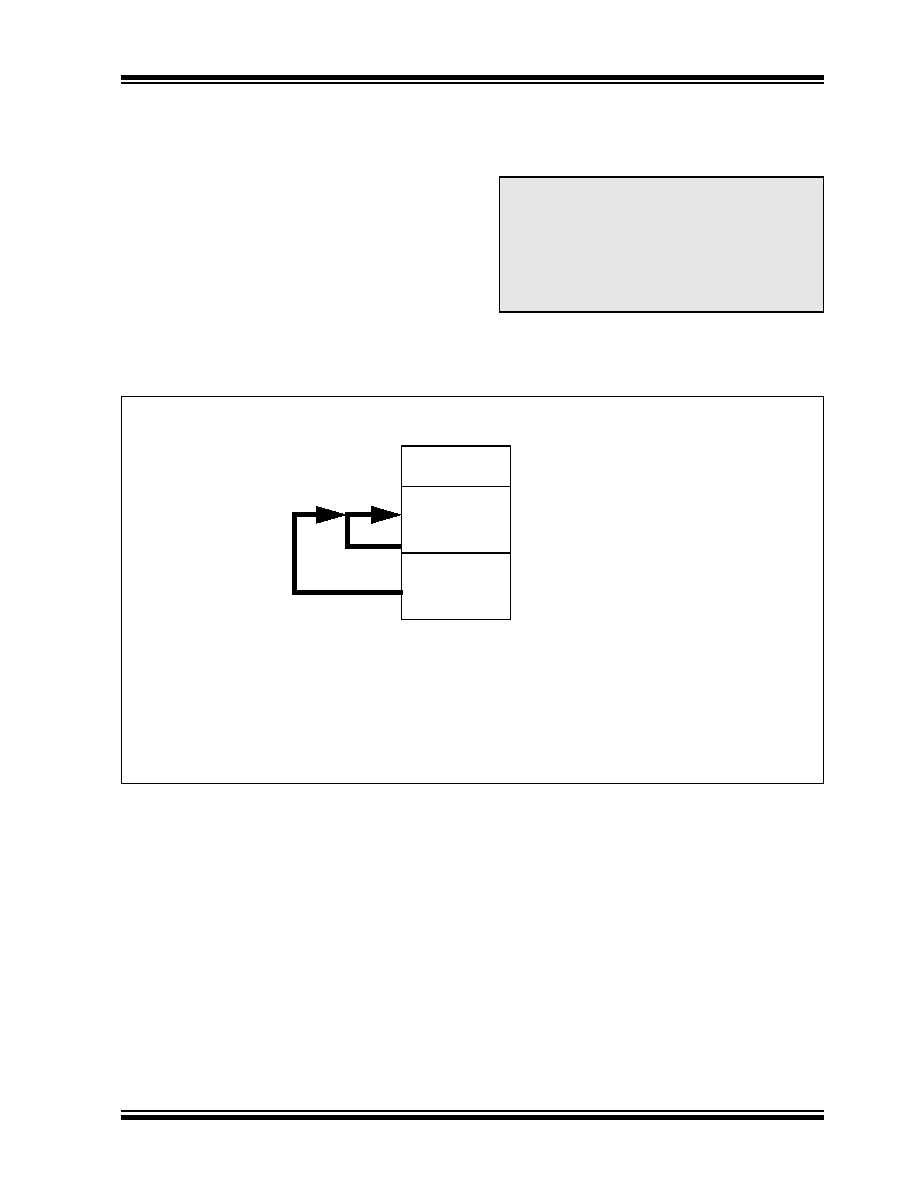
PIC18F2450/4450
� 2006 Microchip Technology Inc.
Advance Information
DS39760A-page 207
18.5.1
PROGRAM MEMORY
CODE PROTECTION
The program memory may be read to or written from
any location using the table read and table write
instructions. The device ID may be read with table
reads. The Configuration registers may be read and
written with the table read and table write instructions.
In normal execution mode, the CPn bits have no direct
effect. CPn bits inhibit external reads and writes. A
block of user memory may be protected from table
writes if the WRTn Configuration bit is `0'. The EBTRn
bits control table reads. For a block of user memory
with the EBTRn bit set to `0', a table read instruction
that executes from within that block is allowed to read.
A table read instruction that executes from a location
outside of that block is not allowed to read and will
result in reading `0's. Figures207 through208 illustrate
table write and table read protection.
FIGURE 18-6:
TABLE WRITE (WRTn) DISALLOWED
Note:
Code protection bits may only be written to
a `0' from a `1' state. It is not possible to
write a `1' to a bit in the `0' state. Code
protection bits are only set to `1' by a full
Chip Erase or Block Erase function. The
full Chip Erase and Block Erase functions
can only be initiated via ICSP operation or
an external programmer.
000000h
000FFFh
001000h
001FFFh
002000h
003FFFh
WRTB, EBTRB = 11
WRT0, EBTR0 = 01
WRT1, EBTR1 = 11
WRT2, EBTR2 = 11
WRT3, EBTR3 = 11
TBLWT*
TBLPTR = 0008FFh
PC = 001FFEh
Register Values
Program Memory
Configuration Bit Settings
Results: All table writes disabled to Blockn whenever WRTn = 0.
0007FFh
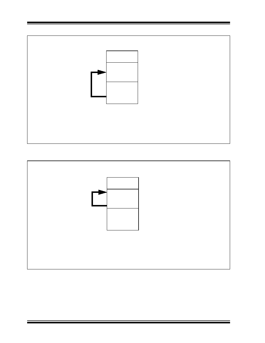
PIC18F2450/4450
DS39760A-page 208
Advance Information
� 2006 Microchip Technology Inc.
FIGURE 18-7:
EXTERNAL BLOCK TABLE READ (EBTRn) DISALLOWED
FIGURE 18-8:
EXTERNAL BLOCK TABLE READ (EBTRn) ALLOWED
WRTB, EBTRB = 11
WRT0, EBTR0 = 10
WRT1, EBTR1 = 11
TBLRD*
TBLPTR = 0008FFh
PC = 003FFEh
Results: All table reads from external blocks to Blockn are disabled whenever EBTRn = 0.
TABLAT register returns a value of `0'.
Register Values
Program Memory
Configuration Bit Settings
000000h
000FFFh
001000h
001FFFh
002000h
003FFFh
0007FFh
WRTB, EBTRB = 11
WRT0, EBTR0 = 10
WRT1, EBTR1 = 11
TBLRD*
TBLPTR = 0008FFh
PC = 001FFEh
Register Values
Program Memory
Configuration Bit Settings
Results: Table reads permitted within Blockn, even when EBTRBn = 0.
TABLAT register returns the value of the data at the location TBLPTR.
000000h
000FFFh
001000h
001FFFh
002000h
003FFFh
0007FFh

PIC18F2450/4450
� 2006 Microchip Technology Inc.
Advance Information
DS39760A-page 209
18.5.2
CONFIGURATION REGISTER
PROTECTION
The Configuration registers can be write-protected.
The WRTC bit controls protection of the Configuration
registers. In normal execution mode, the WRTC bit is
readable only. WRTC can only be written via ICSP
operation or an external programmer.
18.6
ID Locations
Eight memory locations (200000h-200007h) are
designated as ID locations, where the user can store
checksum or other code identification numbers. These
locations are both readable and writable during normal
execution through the TBLRD and TBLWT instructions
or during program/verify. The ID locations can be read
when the device is code-protected.
18.7
In-Circuit Serial Programming
PIC18F2450/4450 microcontrollers can be serially
programmed while in the end application circuit. This is
simply done with two lines for clock and data and three
other lines for power, ground and the programming
voltage. This allows customers to manufacture boards
with unprogrammed devices and then program the
microcontroller just before shipping the product. This
also allows the most recent firmware or a custom
firmware to be programmed.
18.8
In-Circuit Debugger
When the DEBUG Configuration bit is programmed to
a `0', the In-Circuit Debugger functionality is enabled.
This function allows simple debugging functions when
used with MPLAB
�
IDE. When the microcontroller has
this feature enabled, some resources are not available
for general use. Table 18-4 shows which resources are
required by the background debugger.
TABLE 18-4:
DEBUGGER RESOURCES
To use the In-Circuit Debugger function of the
microcontroller, the design must implement In-Circuit
Serial Programming connections to MCLR/V
PP
/RE3,
V
DD
, V
SS
, RB7 and RB6. This will interface to the
In-Circuit Debugger module available from Microchip
or one of the third party development tool companies.
18.9
Special ICPORT Features
(Designated Packages Only)
Under specific circumstances, the No Connect (NC)
pins of PIC18F4450 devices in 44-pin TQFP packages
can provide additional functionality. These features are
controlled by device Configuration bits and are
available only in this package type and pin count.
18.9.1
DEDICATED ICD/ICSP PORT
The 44-pin TQFP devices can use NC pins to provide an
alternate port for In-Circuit Debugging (ICD) and In-
Circuit Serial Programming (ICSP). These pins are
collectively known as the dedicated ICSP/ICD port, since
they are not shared with any other function of the device.
When implemented, the dedicated port activates three
NC pins to provide an alternate device Reset, data and
clock ports. None of these ports overlap with standard
I/O pins, making the I/O pins available to the user's
application.
The dedicated ICSP/ICD port is enabled by setting the
ICPRT Configuration bit. The port functions the same
way as the legacy ICSP/ICD port on RB6/RB7.
Table 18-5 identifies the functionally equivalent pins for
ICSP and ICD purposes.
TABLE 18-5:
EQUIVALENT PINS FOR
LEGACY AND DEDICATED
ICD/ICSPTM PORTS
I/O pins:
RB6, RB7
Stack:
2 levels
Program Memory:
512 bytes
Data Memory:
10 bytes
Pin Name
Pin
Type
Pin Function
Legacy
Port
Dedicated
Port
MCLR/V
PP
/
RE3
NC/ICRST/
ICV
PP
P
Device Reset and
Programming
Enable
RB6/KBI2/
PGC
NC/ICCK/
ICPGC
I
Serial Clock
RB7/KBI3/
PGD
NC/ICDT/
ICPGD
I/O
Serial Data
Legend:
I = Input, O = Output, P = Power

PIC18F2450/4450
DS39760A-page 210
Advance Information
� 2006 Microchip Technology Inc.
Even when the dedicated port is enabled, the ICSP and
ICD functions remain available through the legacy port.
When V
IH
is seen on the MCLR/V
PP
/RE3 pin, the state
of the ICRST/ICV
PP
pin is ignored.
18.9.2
28-PIN EMULATION
PIC18F4450 devices in 44-pin TQFP packages also
have the ability to change their configuration under
external control for debugging purposes. This allows
the device to behave as if it were a PIC18F2455/2550
28-pin device.
This 28-pin Configuration mode is controlled through a
single pin, NC/ICPORTS. Connecting this pin to V
SS
forces the device to function as a 28-pin device.
Features normally associated with the 40/44-pin
devices are disabled, along with their corresponding
control registers and bits. On the other hand,
connecting the pin to V
DD
forces the device to function
in its default configuration.
The configuration option is only available when
background debugging and the dedicated ICD/ICSP
port are both enabled (DEBUG Configuration bit is
clear and ICPRT Configuration bit is set). When
disabled, NC/ICPORTS is a No Connect pin.
18.10 Single-Supply ICSP Programming
The LVP Configuration bit enables Single-Supply
ICSP Programming (formerly known as
Low-Voltage
ICSP Programming or LVP). When Single-Supply
Programming is enabled, the microcontroller can be
programmed without requiring high voltage being
applied to the MCLR/V
PP
/RE3 pin, but the RB5/KBI1/
PGM pin is then dedicated to controlling Program
mode entry and is not available as a general purpose
I/O pin.
While programming using Single-Supply Program-
ming, V
DD
is applied to the MCLR/V
PP
/RE3 pin as in
normal execution mode. To enter Programming mode,
V
DD
is applied to the PGM pin.
If Single-Supply ICSP Programming mode will not be
used, the LVP bit can be cleared. RB5/KBI1/PGM then
becomes available as the digital I/O pin, RB5. The LVP
bit may be set or cleared only when using standard
high-voltage programming (V
IHH
applied to the MCLR/
V
PP
/RE3 pin). Once LVP has been disabled, only the
standard high-voltage programming is available and
must be used to program the device.
Memory that is not code-protected can be erased using
either a Block Erase, or erased row by row, then written
at any specified V
DD
. If code-protected memory is to be
erased, a Block Erase is required. If a Block Erase is to
be performed when using Low-Voltage Programming,
the device must be supplied with V
DD
of 4.5V to 5.5V.
Note 1: The ICPRT Configuration bit can only be
programmed through the default ICSP
port.
2: The ICPRT Configuration bit must be
maintained clear for all 28-pin and 40-pin
devices; otherwise, unexpected operation
may occur.
Note 1: High-Voltage Programming is always
available, regardless of the state of the
LVP bit, by applying V
IHH
to the MCLR pin.
2: While in Low-Voltage ICSP Programming
mode, the RB5 pin can no longer be used
as a general purpose I/O pin and should
be held low during normal operation.
3: When using Low-Voltage ICSP Program-
ming (LVP) and the pull-ups on PORTB
are enabled, bit 5 in the TRISB register
must be cleared to disable the pull-up on
RB5 and ensure the proper operation of
the device.
4: If the device Master Clear is disabled,
verify that either of the following is done to
ensure proper entry into ICSP mode:
a) disable Low-Voltage Programming
(CONFIG4L<2> = 0); or
b) make certain that RB5/KBI1/PGM
is held low during entry into ICSP.

PIC18F2450/4450
� 2006 Microchip Technology Inc.
Advance Information
DS39760A-page 211
19.0
INSTRUCTION SET SUMMARY
PIC18F2450/4450 devices incorporate the standard
set of 75 PIC18 core instructions, as well as an
extended set of eight new instructions for the
optimization of code that is recursive or that utilizes a
software stack. The extended set is discussed later in
this section.
19.1
Standard Instruction Set
The standard PIC18 instruction set adds many
enhancements to the previous PICmicro instruction
sets, while maintaining an easy migration from these
PICmicro instruction sets. Most instructions are a
single program memory word (16 bits) but there are
four instructions that require two program memory
locations.
Each single-word instruction is a 16-bit word divided
into an opcode, which specifies the instruction type and
one or more operands, which further specify the
operation of the instruction.
The instruction set is highly orthogonal and is grouped
into four basic categories:
� Byte-oriented operations
� Bit-oriented operations
� Literal operations
� Control operations
The PIC18 instruction set summary in Table 19-2 lists
byte-oriented, bit-oriented, literal and control
operations. Table 19-1 shows the opcode field
descriptions.
Most byte-oriented instructions have three operands:
1.
The file register (specified by `f')
2.
The destination of the result (specified by `d')
3.
The accessed memory (specified by `a')
The file register designator `f' specifies which file
register is to be used by the instruction. The destination
designator `d' specifies where the result of the
operation is to be placed. If `d' is zero, the result is
placed in the WREG register. If `d' is one, the result is
placed in the file register specified in the instruction.
All bit-oriented instructions have three operands:
1.
The file register (specified by `f')
2.
The bit in the file register (specified by `b')
3.
The accessed memory (specified by `a')
The bit field designator `b' selects the number of the bit
affected by the operation, while the file register
designator `f' represents the number of the file in which
the bit is located.
The literal instructions may use some of the following
operands:
� A literal value to be loaded into a file register
(specified by `k')
� The desired FSR register to load the literal value
into (specified by `f')
� No operand required
(specified by `--')
The control instructions may use some of the following
operands:
� A program memory address (specified by `n')
� The mode of the CALL or RETURN instructions
(specified by `s')
� The mode of the table read and table write
instructions (specified by `m')
� No operand required
(specified by `--')
All instructions are a single word, except for four
double-word instructions. These instructions were
made double-word to contain the required information
in 32 bits. In the second word, the 4 MSbs are `1's. If
this second word is executed as an instruction (by
itself), it will execute as a NOP.
All single-word instructions are executed in a single
instruction cycle, unless a conditional test is true or the
program counter is changed as a result of the instruc-
tion. In these cases, the execution takes two instruction
cycles with the additional instruction cycle(s) executed
as a NOP.
The double-word instructions execute in two instruction
cycles.
One instruction cycle consists of four oscillator periods.
Thus, for an oscillator frequency of 4 MHz, the normal
instruction execution time is 1
s. If a conditional test is
true, or the program counter is changed as a result of
an instruction, the instruction execution time is 2
s.
Two-word branch instructions (if true) would take 3
s.
Figure 19-1 shows the general formats that the
instructions can have. All examples use the convention
`nnh' to represent a hexadecimal number.
The Instruction Set Summary, shown in Table 19-2,
lists the standard instructions recognized by the
Microchip MPASM
TM
Assembler.
Section 19.1.1 "Standard Instruction Set" provides
a description of each instruction.

PIC18F2450/4450
DS39760A-page 212
Advance Information
� 2006 Microchip Technology Inc.
TABLE 19-1:
OPCODE FIELD DESCRIPTIONS
Field
Description
a
RAM access bit
a = 0: RAM location in Access RAM (BSR register is ignored)
a = 1: RAM bank is specified by BSR register
bbb
Bit address within an 8-bit file register (0 to 7).
BSR
Bank Select Register. Used to select the current RAM bank.
C, DC, Z, OV, N
ALU Status bits: Carry, Digit Carry, Zero, Overflow, Negative.
d
Destination select bit
d = 0: store result in WREG
d = 1: store result in file register f
dest
Destination: either the WREG register or the specified register file location.
f
8-bit register file address (00h to FFh) or 2-bit FSR designator (0h to 3h).
f
s
12-bit register file address (000h to FFFh). This is the source address.
f
d
12-bit register file address (000h to FFFh). This is the destination address.
GIE
Global Interrupt Enable bit.
k
Literal field, constant data or label (may be either an 8-bit, 12-bit or a 20-bit value).
label
Label name.
mm
The mode of the TBLPTR register for the table read and table write instructions.
Only used with table read and table write instructions:
*
No change to register (such as TBLPTR with table reads and writes)
*+
Post-Increment register (such as TBLPTR with table reads and writes)
*-
Post-Decrement register (such as TBLPTR with table reads and writes)
+*
Pre-Increment register (such as TBLPTR with table reads and writes)
n
The relative address (2's complement number) for relative branch instructions or the direct address for
Call/Branch and Return instructions.
PC
Program Counter.
PCL
Program Counter Low Byte.
PCH
Program Counter High Byte.
PCLATH
Program Counter High Byte Latch.
PCLATU
Program Counter Upper Byte Latch.
PD
Power-Down bit.
PRODH
Product of Multiply High Byte.
PRODL
Product of Multiply Low Byte.
s
Fast Call/Return mode select bit
s = 0: do not update into/from shadow registers
s = 1: certain registers loaded into/from shadow registers (Fast mode)
TBLPTR
21-bit Table Pointer (points to a program memory location).
TABLAT
8-bit Table Latch.
TO
Time-out bit.
TOS
Top-of-Stack.
u
Unused or unchanged.
WDT
Watchdog Timer.
WREG
Working register (accumulator).
x
Don't care (`0' or `1'). The assembler will generate code with x = 0. It is the recommended form of use for
compatibility with all Microchip software tools.
z
s
7-bit offset value for indirect addressing of register files (source).
z
d
7-bit offset value for indirect addressing of register files (destination).
{ }
Optional argument.
[text]
Indicates an indexed address.
(text)
The contents of text.
[expr]<n>
Specifies bit n of the register indicated by the pointer expr.
Assigned to.
< >
Register bit field.
In the set of.
italics
User-defined term (font is Courier).
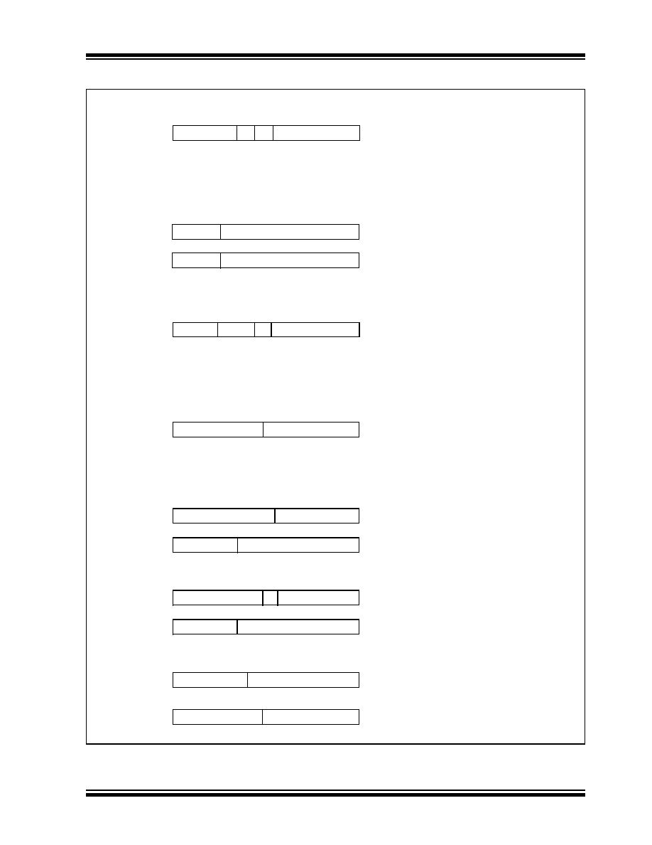
PIC18F2450/4450
� 2006 Microchip Technology Inc.
Advance Information
DS39760A-page 213
FIGURE 19-1:
GENERAL FORMAT FOR INSTRUCTIONS
Byte-oriented file register operations
15 10 9 8 7 0
d = 0 for result destination to be WREG register
OPCODE d a f (FILE #)
d = 1 for result destination to be file register (f)
a = 0 to force Access Bank
Bit-oriented file register operations
15 12 11 9 8 7 0
OPCODE b (BIT #) a f (FILE #)
b = 3-bit position of bit in file register (f)
Literal operations
15 8 7 0
OPCODE k (literal)
k = 8-bit immediate value
Byte to Byte move operations (2-word)
15 12 11 0
OPCODE f (Source FILE #)
CALL
, GOTO and Branch operations
15 8 7 0
OPCODE n<7:0> (literal)
n = 20-bit immediate value
a = 1 for BSR to select bank
f = 8-bit file register address
a = 0 to force Access Bank
a = 1 for BSR to select bank
f = 8-bit file register address
15 12 11 0
1111
n<19:8> (literal)
15 12 11 0
1111 f (Destination FILE #)
f = 12-bit file register address
Control operations
Example Instruction
ADDWF MYREG, W, B
MOVFF MYREG1, MYREG2
BSF MYREG, bit, B
MOVLW 7Fh
GOTO Label
15 8 7 0
OPCODE n<7:0> (literal)
15 12 11 0
1111
n<19:8> (literal)
CALL MYFUNC
15 11 10 0
OPCODE n<10:0> (literal)
S = Fast bit
BRA MYFUNC
15 8 7 0
OPCODE n<7:0> (literal)
BC MYFUNC
S

PIC18F2450/4450
DS39760A-page 214
Advance Information
� 2006 Microchip Technology Inc.
TABLE 19-2:
PIC18FXXXX INSTRUCTION SET
Mnemonic,
Operands
Description
Cycles
16-Bit Instruction Word
Status
Affected
Notes
MSb
LSb
BYTE-ORIENTED OPERATIONS
ADDWF
ADDWFC
ANDWF
CLRF
COMF
CPFSEQ
CPFSGT
CPFSLT
DECF
DECFSZ
DCFSNZ
INCF
INCFSZ
INFSNZ
IORWF
MOVF
MOVFF
MOVWF
MULWF
NEGF
RLCF
RLNCF
RRCF
RRNCF
SETF
SUBFWB
SUBWF
SUBWFB
SWAPF
TSTFSZ
XORWF
f, d, a
f, d, a
f, d, a
f, a
f, d, a
f, a
f, a
f, a
f, d, a
f, d, a
f, d, a
f, d, a
f, d, a
f, d, a
f, d, a
f, d, a
f
s
, f
d
f, a
f, a
f, a
f, d, a
f, d, a
f, d, a
f, d, a
f, a
f, d, a
f, d, a
f, d, a
f, d, a
f, a
f, d, a
Add WREG and f
Add WREG and Carry bit to f
AND WREG with f
Clear f
Complement f
Compare f with WREG, skip =
Compare f with WREG, skip >
Compare f with WREG, skip <
Decrement f
Decrement f, Skip if 0
Decrement f, Skip if Not 0
Increment f
Increment f, Skip if 0
Increment f, Skip if Not 0
Inclusive OR WREG with f
Move f
Move f
s
(source) to 1st word
f
d
(destination) 2nd word
Move WREG to f
Multiply WREG with f
Negate f
Rotate Left f through Carry
Rotate Left f (No Carry)
Rotate Right f through Carry
Rotate Right f (No Carry)
Set f
Subtract f from WREG with
borrow
Subtract WREG from f
Subtract WREG from f with
borrow
Swap nibbles in f
Test f, skip if 0
Exclusive OR WREG with f
1
1
1
1
1
1 (2 or 3)
1 (2 or 3)
1 (2 or 3)
1
1 (2 or 3)
1 (2 or 3)
1
1 (2 or 3)
1 (2 or 3)
1
1
2
1
1
1
1
1
1
1
1
1
1
1
1
1 (2 or 3)
1
0010
0010
0001
0110
0001
0110
0110
0110
0000
0010
0100
0010
0011
0100
0001
0101
1100
1111
0110
0000
0110
0011
0100
0011
0100
0110
0101
0101
0101
0011
0110
0001
01da
00da
01da
101a
11da
001a
010a
000a
01da
11da
11da
10da
11da
10da
00da
00da
ffff
ffff
111a
001a
110a
01da
01da
00da
00da
100a
01da
11da
10da
10da
011a
10da
ffff
ffff
ffff
ffff
ffff
ffff
ffff
ffff
ffff
ffff
ffff
ffff
ffff
ffff
ffff
ffff
ffff
ffff
ffff
ffff
ffff
ffff
ffff
ffff
ffff
ffff
ffff
ffff
ffff
ffff
ffff
ffff
ffff
ffff
ffff
ffff
ffff
ffff
ffff
ffff
ffff
ffff
ffff
ffff
ffff
ffff
ffff
ffff
ffff
ffff
ffff
ffff
ffff
ffff
ffff
ffff
ffff
ffff
ffff
ffff
ffff
ffff
ffff
ffff
C, DC, Z, OV, N
C, DC, Z, OV, N
Z, N
Z
Z, N
None
None
None
C, DC, Z, OV, N
None
None
C, DC, Z, OV, N
None
None
Z, N
Z, N
None
None
None
C, DC, Z, OV, N
C, Z, N
Z, N
C, Z, N
Z, N
None
C, DC, Z, OV, N
C, DC, Z, OV, N
C, DC, Z, OV, N
None
None
Z, N
1, 2
1, 2
1,2
2
1, 2
4
4
1, 2
1, 2, 3, 4
1, 2, 3, 4
1, 2
1, 2, 3, 4
4
1, 2
1, 2
1
1, 2
1, 2
1, 2
1, 2
4
1, 2
Note 1:
When a PORT register is modified as a function of itself (e.g., MOVF PORTB, 1, 0), the value used will be that
value present on the pins themselves. For example, if the data latch is `1' for a pin configured as an input and is
driven low by an external device, the data will be written back with a `0'.
2:
If this instruction is executed on the TMR0 register (and where applicable, `d' = 1), the prescaler will be cleared if
assigned.
3:
If the Program Counter (PC) is modified or a conditional test is true, the instruction requires two cycles. The
second cycle is executed as a NOP.
4:
Some instructions are two-word instructions. The second word of these instructions will be executed as a NOP
unless the first word of the instruction retrieves the information embedded in these 16 bits. This ensures that all
program memory locations have a valid instruction.

PIC18F2450/4450
� 2006 Microchip Technology Inc.
Advance Information
DS39760A-page 215
BIT-ORIENTED OPERATIONS
BCF
BSF
BTFSC
BTFSS
BTG
f, b, a
f, b, a
f, b, a
f, b, a
f, d, a
Bit Clear f
Bit Set f
Bit Test f, Skip if Clear
Bit Test f, Skip if Set
Bit Toggle f
1
1
1 (2 or 3)
1 (2 or 3)
1
1001
1000
1011
1010
0111
bbba
bbba
bbba
bbba
bbba
ffff
ffff
ffff
ffff
ffff
ffff
ffff
ffff
ffff
ffff
None
None
None
None
None
1, 2
1, 2
3, 4
3, 4
1, 2
CONTROL OPERATIONS
BC
BN
BNC
BNN
BNOV
BNZ
BOV
BRA
BZ
CALL
CLRWDT
DAW
GOTO
NOP
NOP
POP
PUSH
RCALL
RESET
RETFIE
RETLW
RETURN
SLEEP
n
n
n
n
n
n
n
n
n
n, s
--
--
n
--
--
--
--
n
s
k
s
--
Branch if Carry
Branch if Negative
Branch if Not Carry
Branch if Not Negative
Branch if Not Overflow
Branch if Not Zero
Branch if Overflow
Branch Unconditionally
Branch if Zero
Call subroutine 1st word
2nd word
Clear Watchdog Timer
Decimal Adjust WREG
Go to address 1st word
2nd word
No Operation
No Operation
Pop top of return stack (TOS)
Push top of return stack (TOS)
Relative Call
Software device Reset
Return from interrupt enable
Return with literal in WREG
Return from Subroutine
Go into Standby mode
1 (2)
1 (2)
1 (2)
1 (2)
1 (2)
1 (2)
1 (2)
2
1 (2)
2
1
1
2
1
1
1
1
2
1
2
2
2
1
1110
1110
1110
1110
1110
1110
1110
1101
1110
1110
1111
0000
0000
1110
1111
0000
1111
0000
0000
1101
0000
0000
0000
0000
0000
0010
0110
0011
0111
0101
0001
0100
0nnn
0000
110s
kkkk
0000
0000
1111
kkkk
0000
xxxx
0000
0000
1nnn
0000
0000
1100
0000
0000
nnnn
nnnn
nnnn
nnnn
nnnn
nnnn
nnnn
nnnn
nnnn
kkkk
kkkk
0000
0000
kkkk
kkkk
0000
xxxx
0000
0000
nnnn
1111
0001
kkkk
0001
0000
nnnn
nnnn
nnnn
nnnn
nnnn
nnnn
nnnn
nnnn
nnnn
kkkk
kkkk
0100
0111
kkkk
kkkk
0000
xxxx
0110
0101
nnnn
1111
000s
kkkk
001s
0011
None
None
None
None
None
None
None
None
None
None
TO, PD
C
None
None
None
None
None
None
All
GIE/GIEH,
PEIE/GIEL
None
None
TO, PD
4
TABLE 19-2:
PIC18FXXXX INSTRUCTION SET (CONTINUED)
Mnemonic,
Operands
Description
Cycles
16-Bit Instruction Word
Status
Affected
Notes
MSb
LSb
Note 1:
When a PORT register is modified as a function of itself (e.g., MOVF PORTB, 1, 0), the value used will be that
value present on the pins themselves. For example, if the data latch is `1' for a pin configured as an input and is
driven low by an external device, the data will be written back with a `0'.
2:
If this instruction is executed on the TMR0 register (and where applicable, `d' = 1), the prescaler will be cleared if
assigned.
3:
If the Program Counter (PC) is modified or a conditional test is true, the instruction requires two cycles. The
second cycle is executed as a NOP.
4:
Some instructions are two-word instructions. The second word of these instructions will be executed as a NOP
unless the first word of the instruction retrieves the information embedded in these 16 bits. This ensures that all
program memory locations have a valid instruction.

PIC18F2450/4450
DS39760A-page 216
Advance Information
� 2006 Microchip Technology Inc.
LITERAL OPERATIONS
ADDLW
ANDLW
IORLW
LFSR
MOVLB
MOVLW
MULLW
RETLW
SUBLW
XORLW
k
k
k
f, k
k
k
k
k
k
k
Add literal and WREG
AND literal with WREG
Inclusive OR literal with WREG
Move literal (12-bit) 2nd word
to FSR(f)
1st word
Move literal to BSR<3:0>
Move literal to WREG
Multiply literal with WREG
Return with literal in WREG
Subtract WREG from literal
Exclusive OR literal with WREG
1
1
1
2
1
1
1
2
1
1
0000
0000
0000
1110
1111
0000
0000
0000
0000
0000
0000
1111
1011
1001
1110
0000
0001
1110
1101
1100
1000
1010
kkkk
kkkk
kkkk
00ff
kkkk
0000
kkkk
kkkk
kkkk
kkkk
kkkk
kkkk
kkkk
kkkk
kkkk
kkkk
kkkk
kkkk
kkkk
kkkk
kkkk
kkkk
C, DC, Z, OV, N
Z, N
Z, N
None
None
None
None
None
C, DC, Z, OV, N
Z, N
DATA MEMORY
PROGRAM MEMORY OPERATIONS
TBLRD*
TBLRD*+
TBLRD*-
TBLRD+*
TBLWT*
TBLWT*+
TBLWT*-
TBLWT+*
Table Read
Table Read with post-increment
Table Read with post-decrement
Table Read with pre-increment
Table Write
Table Write with post-increment
Table Write with post-decrement
Table Write with pre-increment
2
2
0000
0000
0000
0000
0000
0000
0000
0000
0000
0000
0000
0000
0000
0000
0000
0000
0000
0000
0000
0000
0000
0000
0000
0000
1000
1001
1010
1011
1100
1101
1110
1111
None
None
None
None
None
None
None
None
TABLE 19-2:
PIC18FXXXX INSTRUCTION SET (CONTINUED)
Mnemonic,
Operands
Description
Cycles
16-Bit Instruction Word
Status
Affected
Notes
MSb
LSb
Note 1:
When a PORT register is modified as a function of itself (e.g., MOVF PORTB, 1, 0), the value used will be that
value present on the pins themselves. For example, if the data latch is `1' for a pin configured as an input and is
driven low by an external device, the data will be written back with a `0'.
2:
If this instruction is executed on the TMR0 register (and where applicable, `d' = 1), the prescaler will be cleared if
assigned.
3:
If the Program Counter (PC) is modified or a conditional test is true, the instruction requires two cycles. The
second cycle is executed as a NOP.
4:
Some instructions are two-word instructions. The second word of these instructions will be executed as a NOP
unless the first word of the instruction retrieves the information embedded in these 16 bits. This ensures that all
program memory locations have a valid instruction.
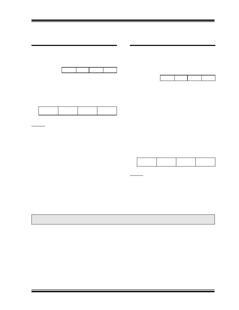
PIC18F2450/4450
� 2006 Microchip Technology Inc.
Advance Information
DS39760A-page 217
19.1.1
STANDARD INSTRUCTION SET
ADDLW
ADD Literal to W
Syntax:
ADDLW k
Operands:
0
k 255
Operation:
(W) + k
W
Status Affected:
N, OV, C, DC, Z
Encoding:
0000
1111
kkkk
kkkk
Description:
The contents of W are added to the
8-bit literal `k' and the result is placed in
W.
Words:
1
Cycles:
1
Q Cycle Activity:
Q1
Q2
Q3
Q4
Decode
Read
literal `k'
Process
Data
Write to W
Example:
ADDLW
15h
Before Instruction
W
=
10h
After Instruction
W = 25h
ADDWF
ADD W to f
Syntax:
ADDWF f {,d {,a}}
Operands:
0
f 255
d
[0,1]
a
[0,1]
Operation:
(W) + (f)
dest
Status Affected:
N, OV, C, DC, Z
Encoding:
0010
01da
ffff
ffff
Description:
Add W to register `f'. If `d' is `0', the
result is stored in W. If `d' is `1', the
result is stored back in register `f'
(default).
If `a' is `0', the Access Bank is selected.
If `a' is `1', the BSR is used to select the
GPR bank (default).
If `a' is `0' and the extended instruction
set is enabled, this instruction operates
in Indexed Literal Offset Addressing
mode whenever f
95 (5Fh). See
Section 19.2.3 "Byte-Oriented and
Bit-Oriented Instructions in Indexed
Literal Offset Mode" for details.
Words:
1
Cycles:
1
Q Cycle Activity:
Q1
Q2
Q3
Q4
Decode
Read
register `f'
Process
Data
Write to
destination
Example:
ADDWF
REG,
0, 0
Before Instruction
W
=
17h
REG
=
0C2h
After Instruction
W
=
0D9h
REG
=
0C2h
Note:
All PIC18 instructions may take an optional label argument, preceding the instruction mnemonic, for use in
symbolic addressing. If a label is used, the instruction format then becomes: {label} instruction argument(s).

PIC18F2450/4450
DS39760A-page 218
Advance Information
� 2006 Microchip Technology Inc.
ADDWFC
ADD W and Carry bit to f
Syntax:
ADDWFC f {,d {,a}}
Operands:
0
f 255
d
[0,1]
a
[0,1]
Operation:
(W) + (f) + (C)
dest
Status Affected:
N, OV, C, DC, Z
Encoding:
0010
00da
ffff
ffff
Description:
Add W, the Carry flag and data memory
location `f'. If `d' is `0', the result is
placed in W. If `d' is `1', the result is
placed in data memory location `f'.
If `a' is `0', the Access Bank is selected.
If `a' is `1', the BSR is used to select the
GPR bank (default).
If `a' is `0' and the extended instruction
set is enabled, this instruction operates
in Indexed Literal Offset Addressing
mode whenever f
95 (5Fh). See
Section 19.2.3 "Byte-Oriented and
Bit-Oriented Instructions in Indexed
Literal Offset Mode" for details.
Words:
1
Cycles:
1
Q Cycle Activity:
Q1
Q2
Q3
Q4
Decode
Read
register `f'
Process
Data
Write to
destination
Example:
ADDWFC
REG,
0, 1
Before Instruction
Carry bit =
1
REG
=
02h
W
=
4Dh
After Instruction
Carry bit =
0
REG
=
02h
W
=
50h
ANDLW
AND Literal with W
Syntax:
ANDLW k
Operands:
0
k 255
Operation:
(W) .AND. k
W
Status Affected:
N, Z
Encoding:
0000
1011
kkkk
kkkk
Description:
The contents of W are ANDed with the
8-bit literal `k'. The result is placed in W.
Words:
1
Cycles:
1
Q Cycle Activity:
Q1
Q2
Q3
Q4
Decode
Read literal
`k'
Process
Data
Write to W
Example:
ANDLW
05Fh
Before Instruction
W
=
A3h
After Instruction
W
=
03h
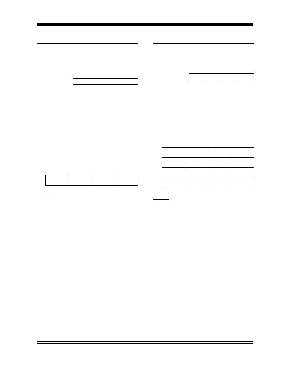
PIC18F2450/4450
� 2006 Microchip Technology Inc.
Advance Information
DS39760A-page 219
ANDWF
AND W with f
Syntax:
ANDWF f {,d {,a}}
Operands:
0
f 255
d
[0,1]
a
[0,1]
Operation:
(W) .AND. (f)
dest
Status Affected:
N, Z
Encoding:
0001
01da
ffff
ffff
Description:
The contents of W are ANDed with
register `f'. If `d' is `0', the result is stored
in W. If `d' is `1', the result is stored back
in register `f' (default).
If `a' is `0', the Access Bank is selected.
If `a' is `1', the BSR is used to select the
GPR bank (default).
If `a' is `0' and the extended instruction
set is enabled, this instruction operates
in Indexed Literal Offset Addressing
mode whenever f
95 (5Fh). See
Section 19.2.3 "Byte-Oriented and
Bit-Oriented Instructions in Indexed
Literal Offset Mode" for details.
Words:
1
Cycles:
1
Q Cycle Activity:
Q1
Q2
Q3
Q4
Decode
Read
register `f'
Process
Data
Write to
destination
Example:
ANDWF
REG,
0, 0
Before Instruction
W
=
17h
REG
=
C2h
After Instruction
W
=
02h
REG
=
C2h
BC
Branch if Carry
Syntax:
BC n
Operands:
-128
n 127
Operation:
if Carry bit is `1'
(PC) + 2 + 2n
PC
Status Affected:
None
Encoding:
1110
0010
nnnn
nnnn
Description:
If the Carry bit is `1', then the program
will branch.
The 2's complement number `2n' is
added to the PC. Since the PC will have
incremented to fetch the next
instruction, the new address will be
PC + 2 + 2n. This instruction is then a
two-cycle instruction.
Words:
1
Cycles:
1(2)
Q Cycle Activity:
If Jump:
Q1
Q2
Q3
Q4
Decode
Read literal
`n'
Process
Data
Write to PC
No
operation
No
operation
No
operation
No
operation
If No Jump:
Q1
Q2
Q3
Q4
Decode
Read literal
`n'
Process
Data
No
operation
Example:
HERE
BC
5
Before Instruction
PC
=
address (HERE)
After Instruction
If Carry
=
1;
PC
= address (HERE + 12)
If Carry
=
0;
PC
= address
(HERE + 2)

PIC18F2450/4450
DS39760A-page 220
Advance Information
� 2006 Microchip Technology Inc.
BCF
Bit Clear f
Syntax:
BCF f, b {,a}
Operands:
0
f 255
0
b 7
a
[0,1]
Operation:
0
f<b>
Status Affected:
None
Encoding:
1001
bbba
ffff
ffff
Description:
Bit `b' in register `f' is cleared.
If `a' is `0', the Access Bank is selected.
If `a' is `1', the BSR is used to select the
GPR bank (default).
If `a' is `0' and the extended instruction
set is enabled, this instruction operates
in Indexed Literal Offset Addressing
mode whenever f
95 (5Fh). See
Section 19.2.3 "Byte-Oriented and
Bit-Oriented Instructions in Indexed
Literal Offset Mode" for details.
Words:
1
Cycles:
1
Q Cycle Activity:
Q1
Q2
Q3
Q4
Decode
Read
register `f'
Process
Data
Write
register `f'
Example:
BCF
FLAG_REG, 7, 0
Before Instruction
FLAG_REG =
C7h
After Instruction
FLAG_REG =
47h
BN
Branch if Negative
Syntax:
BN n
Operands:
-128
n 127
Operation:
if Negative bit is `1'
(PC) + 2 + 2n
PC
Status Affected:
None
Encoding:
1110
0110
nnnn
nnnn
Description:
If the Negative bit is `1', then the
program will branch.
The 2's complement number `2n' is
added to the PC. Since the PC will have
incremented to fetch the next
instruction, the new address will be
PC + 2 + 2n. This instruction is then a
two-cycle instruction.
Words:
1
Cycles:
1(2)
Q Cycle Activity:
If Jump:
Q1
Q2
Q3
Q4
Decode
Read literal
`n'
Process
Data
Write to PC
No
operation
No
operation
No
operation
No
operation
If No Jump:
Q1
Q2
Q3
Q4
Decode
Read literal
`n'
Process
Data
No
operation
Example:
HERE
BN
Jump
Before Instruction
PC
=
address (HERE)
After Instruction
If Negative
=
1;
PC
= address
(Jump)
If Negative
=
0;
PC
= address
(HERE + 2)
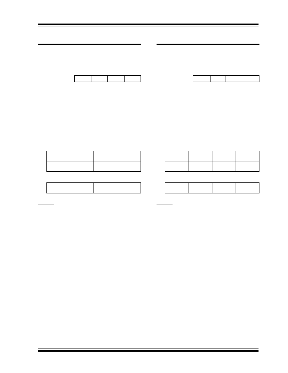
PIC18F2450/4450
� 2006 Microchip Technology Inc.
Advance Information
DS39760A-page 221
BNC
Branch if Not Carry
Syntax:
BNC n
Operands:
-128
n 127
Operation:
if Carry bit is `0'
(PC) + 2 + 2n
PC
Status Affected:
None
Encoding:
1110
0011
nnnn
nnnn
Description:
If the Carry bit is `0', then the program
will branch.
The 2's complement number `2n' is
added to the PC. Since the PC will have
incremented to fetch the next
instruction, the new address will be
PC + 2 + 2n. This instruction is then a
two-cycle instruction.
Words:
1
Cycles:
1(2)
Q Cycle Activity:
If Jump:
Q1
Q2
Q3
Q4
Decode
Read literal
`n'
Process
Data
Write to PC
No
operation
No
operation
No
operation
No
operation
If No Jump:
Q1
Q2
Q3
Q4
Decode
Read literal
`n'
Process
Data
No
operation
Example:
HERE
BNC
Jump
Before Instruction
PC
=
address (HERE)
After Instruction
If Carry
=
0;
PC
= address
(Jump)
If Carry
=
1;
PC
= address (HERE + 2)
BNN
Branch if Not Negative
Syntax:
BNN n
Operands:
-128
n 127
Operation:
if Negative bit is `0'
(PC) + 2 + 2n
PC
Status Affected:
None
Encoding:
1110
0111
nnnn
nnnn
Description:
If the Negative bit is `0', then the
program will branch.
The 2's complement number `2n' is
added to the PC. Since the PC will have
incremented to fetch the next
instruction, the new address will be
PC + 2 + 2n. This instruction is then a
two-cycle instruction.
Words:
1
Cycles:
1(2)
Q Cycle Activity:
If Jump:
Q1
Q2
Q3
Q4
Decode
Read literal
`n'
Process
Data
Write to PC
No
operation
No
operation
No
operation
No
operation
If No Jump:
Q1
Q2
Q3
Q4
Decode
Read literal
`n'
Process
Data
No
operation
Example:
HERE
BNN
Jump
Before Instruction
PC
=
address (HERE)
After Instruction
If Negative
=
0;
PC
= address (Jump)
If Negative
=
1;
PC
= address (HERE + 2)

PIC18F2450/4450
DS39760A-page 222
Advance Information
� 2006 Microchip Technology Inc.
BNOV
Branch if Not Overflow
Syntax:
BNOV n
Operands:
-128
n 127
Operation:
if Overflow bit is `0'
(PC) + 2 + 2n
PC
Status Affected:
None
Encoding:
1110
0101
nnnn
nnnn
Description:
If the Overflow bit is `0', then the
program will branch.
The 2's complement number `2n' is
added to the PC. Since the PC will have
incremented to fetch the next
instruction, the new address will be
PC + 2 + 2n. This instruction is then a
two-cycle instruction.
Words:
1
Cycles:
1(2)
Q Cycle Activity:
If Jump:
Q1
Q2
Q3
Q4
Decode
Read literal
`n'
Process
Data
Write to PC
No
operation
No
operation
No
operation
No
operation
If No Jump:
Q1
Q2
Q3
Q4
Decode
Read literal
`n'
Process
Data
No
operation
Example:
HERE
BNOV
Jump
Before Instruction
PC
=
address (HERE)
After Instruction
If Overflow
=
0;
PC
= address (Jump)
If Overflow
=
1;
PC
= address (HERE + 2)
BNZ
Branch if Not Zero
Syntax:
BNZ n
Operands:
-128
n 127
Operation:
if Zero bit is `0'
(PC) + 2 + 2n
PC
Status Affected:
None
Encoding:
1110
0001
nnnn
nnnn
Description:
If the Zero bit is `0', then the program
will branch.
The 2's complement number `2n' is
added to the PC. Since the PC will have
incremented to fetch the next
instruction, the new address will be
PC + 2 + 2n. This instruction is then a
two-cycle instruction.
Words:
1
Cycles:
1(2)
Q Cycle Activity:
If Jump:
Q1
Q2
Q3
Q4
Decode
Read literal
`n'
Process
Data
Write to PC
No
operation
No
operation
No
operation
No
operation
If No Jump:
Q1
Q2
Q3
Q4
Decode
Read literal
`n'
Process
Data
No
operation
Example:
HERE
BNZ
Jump
Before Instruction
PC
=
address (HERE)
After Instruction
If Zero
=
0;
PC
= address
(Jump)
If Zero
=
1;
PC
= address
(HERE + 2)
PIC18F2450/4450
� 2006 Microchip Technology Inc.
Advance Information
DS39760A-page 223
BRA
Unconditional Branch
Syntax:
BRA n
Operands:
-1024
n 1023
Operation:
(PC) + 2 + 2n
PC
Status Affected:
None
Encoding:
1101
0nnn
nnnn
nnnn
Description:
Add the 2's complement number `2n' to
the PC. Since the PC will have
incremented to fetch the next
instruction, the new address will be
PC + 2 + 2n. This instruction is a
two-cycle instruction.
Words:
1
Cycles:
2
Q Cycle Activity:
Q1
Q2
Q3
Q4
Decode
Read literal
`n'
Process
Data
Write to PC
No
operation
No
operation
No
operation
No
operation
Example:
HERE
BRA
Jump
Before Instruction
PC
=
address (HERE)
After Instruction
PC
= address (Jump)
BSF
Bit Set f
Syntax:
BSF f, b {,a}
Operands:
0
f 255
0
b 7
a
[0,1]
Operation:
1
f<b>
Status Affected:
None
Encoding:
1000
bbba
ffff
ffff
Description:
Bit `b' in register `f' is set.
If `a' is `0', the Access Bank is selected.
If `a' is `1', the BSR is used to select the
GPR bank (default).
If `a' is `0' and the extended instruction
set is enabled, this instruction operates
in Indexed Literal Offset Addressing
mode whenever f
95 (5Fh). See
Section 19.2.3 "Byte-Oriented and
Bit-Oriented Instructions in Indexed
Literal Offset Mode" for details.
Words:
1
Cycles:
1
Q Cycle Activity:
Q1
Q2
Q3
Q4
Decode
Read
register `f'
Process
Data
Write
register `f'
Example:
BSF
FLAG_REG, 7, 1
Before Instruction
FLAG_REG
=
0Ah
After Instruction
FLAG_REG
=
8Ah
PIC18F2450/4450
DS39760A-page 224
Advance Information
� 2006 Microchip Technology Inc.
BTFSC
Bit Test File, Skip if Clear
Syntax:
BTFSC f, b {,a}
Operands:
0
f 255
0
b 7
a
[0,1]
Operation:
skip if (f<b>) = 0
Status Affected:
None
Encoding:
1011
bbba
ffff
ffff
Description:
If bit `b' in register `f' is `0', then the next
instruction is skipped. If bit `b' is `0', then
the next instruction fetched during the
current instruction execution is discarded
and a NOP is executed instead, making
this a two-cycle instruction.
If `a' is `0', the Access Bank is selected. If
`a' is `1', the BSR is used to select the
GPR bank (default).
If `a' is `0' and the extended instruction
set is enabled, this instruction operates in
Indexed Literal Offset Addressing
mode whenever f
95 (5Fh).
See Section 19.2.3 "Byte-Oriented and
Bit-Oriented Instructions in Indexed
Literal Offset Mode" for details.
Words:
1
Cycles:
1(2)
Note:
3 cycles if skip and followed
by a 2-word instruction.
Q Cycle Activity:
Q1
Q2
Q3
Q4
Decode
Read
register `f'
Process
Data
No
operation
If skip:
Q1
Q2
Q3
Q4
No
operation
No
operation
No
operation
No
operation
If skip and followed by 2-word instruction:
Q1
Q2
Q3
Q4
No
operation
No
operation
No
operation
No
operation
No
operation
No
operation
No
operation
No
operation
Example:
HERE
FALSE
TRUE
BTFSC
:
:
FLAG, 1, 0
Before Instruction
PC
=
address (HERE)
After Instruction
If FLAG<1>
=
0;
PC
= address (TRUE)
If FLAG<1>
=
1;
PC
= address (FALSE)
BTFSS
Bit Test File, Skip if Set
Syntax:
BTFSS f, b {,a}
Operands:
0
f 255
0
b < 7
a
[0,1]
Operation:
skip if (f<b>) = 1
Status Affected:
None
Encoding:
1010
bbba
ffff
ffff
Description:
If bit `b' in register `f' is `1', then the next
instruction is skipped. If bit `b' is `1', then
the next instruction fetched during the
current instruction execution is discarded
and a NOP is executed instead, making
this a two-cycle instruction.
If `a' is `0', the Access Bank is selected. If
`a' is `1', the BSR is used to select the
GPR bank (default).
If `a' is `0' and the extended instruction
set is enabled, this instruction operates
in Indexed Literal Offset Addressing
mode whenever f
95 (5Fh).
See Section 19.2.3 "Byte-Oriented and
Bit-Oriented Instructions in Indexed
Literal Offset Mode" for details.
Words:
1
Cycles:
1(2)
Note:
3 cycles if skip and followed
by a 2-word instruction.
Q Cycle Activity:
Q1
Q2
Q3
Q4
Decode
Read
register `f'
Process
Data
No
operation
If skip:
Q1
Q2
Q3
Q4
No
operation
No
operation
No
operation
No
operation
If skip and followed by 2-word instruction:
Q1
Q2
Q3
Q4
No
operation
No
operation
No
operation
No
operation
No
operation
No
operation
No
operation
No
operation
Example:
HERE
FALSE
TRUE
BTFSS
:
:
FLAG, 1, 0
Before Instruction
PC
= address (HERE)
After Instruction
If FLAG<1>
=
0;
PC
= address (FALSE)
If FLAG<1>
=
1;
PC
= address
(TRUE)
PIC18F2450/4450
� 2006 Microchip Technology Inc.
Advance Information
DS39760A-page 225
BTG
Bit Toggle f
Syntax:
BTG f, b {,a}
Operands:
0
f 255
0
b < 7
a
[0,1]
Operation:
(f<b>)
f<b>
Status Affected:
None
Encoding:
0111
bbba
ffff
ffff
Description:
Bit `b' in data memory location `f' is
inverted.
If `a' is `0', the Access Bank is selected.
If `a' is `1', the BSR is used to select the
GPR bank (default).
If `a' is `0' and the extended instruction
set is enabled, this instruction operates
in Indexed Literal Offset Addressing
mode whenever f
95 (5Fh). See
Section 19.2.3 "Byte-Oriented and
Bit-Oriented Instructions in Indexed
Literal Offset Mode" for details.
Words:
1
Cycles:
1
Q Cycle Activity:
Q1
Q2
Q3
Q4
Decode
Read
register `f'
Process
Data
Write
register `f'
Example:
BTG
PORTC,
4, 0
Before Instruction:
PORTC
=
0111 0101
[75h]
After Instruction:
PORTC
=
0110 0101
[65h]
BOV
Branch if Overflow
Syntax:
BOV n
Operands:
-128
n 127
Operation:
if Overflow bit is `1'
(PC) + 2 + 2n
PC
Status Affected:
None
Encoding:
1110
0100
nnnn
nnnn
Description:
If the Overflow bit is `1', then the
program will branch.
The 2's complement number `2n' is
added to the PC. Since the PC will have
incremented to fetch the next
instruction, the new address will be
PC + 2 + 2n. This instruction is then a
two-cycle instruction.
Words:
1
Cycles:
1(2)
Q Cycle Activity:
If Jump:
Q1
Q2
Q3
Q4
Decode
Read literal
`n'
Process
Data
Write to PC
No
operation
No
operation
No
operation
No
operation
If No Jump:
Q1
Q2
Q3
Q4
Decode
Read literal
`n'
Process
Data
No
operation
Example:
HERE
BOV
Jump
Before Instruction
PC
=
address (HERE)
After Instruction
If Overflow
=
1;
PC
= address (Jump)
If Overflow
=
0;
PC
= address (HERE + 2)

PIC18F2450/4450
DS39760A-page 226
Advance Information
� 2006 Microchip Technology Inc.
BZ
Branch if Zero
Syntax:
BZ n
Operands:
-128
n 127
Operation:
if Zero bit is `1'
(PC) + 2 + 2n
PC
Status Affected:
None
Encoding:
1110
0000
nnnn
nnnn
Description:
If the Zero bit is `1', then the program
will branch.
The 2's complement number `2n' is
added to the PC. Since the PC will have
incremented to fetch the next
instruction, the new address will be
PC + 2 + 2n. This instruction is then a
two-cycle instruction.
Words:
1
Cycles:
1(2)
Q Cycle Activity:
If Jump:
Q1
Q2
Q3
Q4
Decode
Read literal
`n'
Process
Data
Write to PC
No
operation
No
operation
No
operation
No
operation
If No Jump:
Q1
Q2
Q3
Q4
Decode
Read literal
`n'
Process
Data
No
operation
Example:
HERE
BZ
Jump
Before Instruction
PC
=
address (HERE)
After Instruction
If Zero
=
1;
PC
= address (Jump)
If Zero
=
0;
PC
= address (HERE + 2)
CALL
Subroutine Call
Syntax:
CALL k {,s}
Operands:
0
k 1048575
s
[0,1]
Operation:
(PC) + 4
TOS,
k
PC<20:1>,
if s = 1
(W)
WS,
(STATUS)
STATUSS,
(BSR)
BSRS
Status Affected:
None
Encoding:
1st word (k<7:0>)
2nd word(k<19:8>)
1110
1111
110s
k
19
kkk
k
7
kkk
kkkk
kkkk
0
kkkk
8
Description:
Subroutine call of entire 2-Mbyte
memory range. First, return address
(PC + 4) is pushed onto the return
stack. If `s' = 1, the W, STATUS and
BSR
registers are also pushed into their
respective shadow registers, WS,
STATUSS and BSRS. If `s' = 0, no
update occurs (default). Then, the
20-bit value `k' is loaded into PC<20:1>.
CALL
is a two-cycle instruction.
Words:
2
Cycles:
2
Q Cycle Activity:
Q1
Q2
Q3
Q4
Decode
Read literal
`k'<7:0>,
Push PC to
stack
Read literal
`k'<19:8>,
Write to PC
No
operation
No
operation
No
operation
No
operation
Example:
HERE
CALL THERE,1
Before Instruction
PC
=
address (HERE)
After Instruction
PC
=
address (THERE)
TOS
=
address (HERE + 4)
WS
=
W
BSRS
=
BSR
STATUSS = STATUS
PIC18F2450/4450
� 2006 Microchip Technology Inc.
Advance Information
DS39760A-page 227
CLRF
Clear f
Syntax:
CLRF f {,a}
Operands:
0
f 255
a
[0,1]
Operation:
000h
f,
1
Z
Status Affected:
Z
Encoding:
0110
101a
ffff
ffff
Description:
Clears the contents of the specified
register.
If `a' is `0', the Access Bank is selected.
If `a' is `1', the BSR is used to select the
GPR bank (default).
If `a' is `0' and the extended instruction
set is enabled, this instruction operates
in Indexed Literal Offset Addressing
mode whenever f
95 (5Fh). See
Section 19.2.3 "Byte-Oriented and
Bit-Oriented Instructions in Indexed
Literal Offset Mode" for details.
Words:
1
Cycles:
1
Q Cycle Activity:
Q1
Q2
Q3
Q4
Decode
Read
register `f'
Process
Data
Write
register `f'
Example:
CLRF
FLAG_REG,1
Before Instruction
FLAG_REG
=
5Ah
After Instruction
FLAG_REG
=
00h
CLRWDT
Clear Watchdog Timer
Syntax:
CLRWDT
Operands:
None
Operation:
000h
WDT,
000h
WDT postscaler,
1
TO,
1
PD
Status Affected:
TO, PD
Encoding:
0000
0000
0000
0100
Description:
CLRWDT
instruction resets the
Watchdog Timer. It also resets the
postscaler of the WDT. Status bits, TO
and PD, are set.
Words:
1
Cycles:
1
Q Cycle Activity:
Q1
Q2
Q3
Q4
Decode
No
operation
Process
Data
No
operation
Example:
CLRWDT
Before Instruction
WDT Counter
=
?
After Instruction
WDT Counter
=
00h
WDT Postscaler
=
0
TO
=
1
PD
=
1

PIC18F2450/4450
DS39760A-page 228
Advance Information
� 2006 Microchip Technology Inc.
COMF
Complement f
Syntax:
COMF f {,d {,a}}
Operands:
0
f 255
d
[0,1]
a
[0,1]
Operation:
(f)
dest
Status Affected:
N, Z
Encoding:
0001
11da
ffff
ffff
Description:
The contents of register `f' are
complemented. If `d' is `0', the result is
stored in W. If `d' is `1', the result is
stored back in register `f' (default).
If `a' is `0', the Access Bank is selected.
If `a' is `1', the BSR is used to select the
GPR bank (default).
If `a' is `0' and the extended instruction
set is enabled, this instruction operates
in Indexed Literal Offset Addressing
mode whenever f
95 (5Fh). See
Section 19.2.3 "Byte-Oriented and
Bit-Oriented Instructions in Indexed
Literal Offset Mode" for details.
Words:
1
Cycles:
1
Q Cycle Activity:
Q1
Q2
Q3
Q4
Decode
Read
register `f'
Process
Data
Write to
destination
Example:
COMF
REG,
0, 0
Before Instruction
REG
=
13h
After Instruction
REG
=
13h
W
=
ECh
CPFSEQ
Compare f with W, Skip if f = W
Syntax:
CPFSEQ f {,a}
Operands:
0
f 255
a
[0,1]
Operation:
(f) � (W),
skip if (f) = (W)
(unsigned comparison)
Status Affected:
None
Encoding:
0110
001a
ffff
ffff
Description:
Compares the contents of data memory
location `f' to the contents of W by
performing an unsigned subtraction.
If `f' = W, then the fetched instruction is
discarded and a NOP is executed
instead, making this a two-cycle
instruction.
If `a' is `0', the Access Bank is selected.
If `a' is `1', the BSR is used to select the
GPR bank (default).
If `a' is `0' and the extended instruction
set is enabled, this instruction operates
in Indexed Literal Offset Addressing
mode whenever f
95 (5Fh). See
Section 19.2.3 "Byte-Oriented and
Bit-Oriented Instructions in Indexed
Literal Offset Mode" for details.
Words:
1
Cycles:
1(2)
Note:
3 cycles if skip and followed
by a 2-word instruction.
Q Cycle Activity:
Q1
Q2
Q3
Q4
Decode
Read
register `f'
Process
Data
No
operation
If skip:
Q1
Q2
Q3
Q4
No
operation
No
operation
No
operation
No
operation
If skip and followed by 2-word instruction:
Q1
Q2
Q3
Q4
No
operation
No
operation
No
operation
No
operation
No
operation
No
operation
No
operation
No
operation
Example:
HERE CPFSEQ REG, 0
NEQUAL :
EQUAL :
Before Instruction
PC Address
=
HERE
W
=
?
REG
=
?
After Instruction
If REG
=
W;
PC =
Address (EQUAL)
If REG
W;
PC =
Address (NEQUAL)
PIC18F2450/4450
� 2006 Microchip Technology Inc.
Advance Information
DS39760A-page 229
CPFSGT
Compare f with W, Skip if f > W
Syntax:
CPFSGT f {,a}
Operands:
0
f 255
a
[0,1]
Operation:
(f) �
(W),
skip if (f) > (W)
(unsigned comparison)
Status Affected:
None
Encoding:
0110
010a
ffff
ffff
Description:
Compares the contents of data memory
location `f' to the contents of the W by
performing an unsigned subtraction.
If the contents of `f' are greater than the
contents of WREG, then the fetched
instruction is discarded and a NOP is
executed instead, making this a
two-cycle instruction.
If `a' is `0', the Access Bank is selected.
If `a' is `1', the BSR is used to select the
GPR bank (default).
If `a' is `0' and the extended instruction
set is enabled, this instruction operates
in Indexed Literal Offset Addressing
mode whenever f
95 (5Fh). See
Section 19.2.3 "Byte-Oriented and
Bit-Oriented Instructions in Indexed
Literal Offset Mode" for details.
Words:
1
Cycles:
1(2)
Note: 3 cycles if skip and followed
by a 2-word instruction.
Q Cycle Activity:
Q1
Q2
Q3
Q4
Decode
Read
register `f'
Process
Data
No
operation
If skip:
Q1
Q2
Q3
Q4
No
operation
No
operation
No
operation
No
operation
If skip and followed by 2-word instruction:
Q1
Q2
Q3
Q4
No
operation
No
operation
No
operation
No
operation
No
operation
No
operation
No
operation
No
operation
Example:
HERE CPFSGT REG, 0
NGREATER :
GREATER :
Before Instruction
PC =
Address (HERE)
W
=
?
After Instruction
If REG
> W;
PC =
Address (GREATER)
If REG
W;
PC
= Address (NGREATER)
CPFSLT
Compare f with W, Skip if f < W
Syntax:
CPFSLT f {,a}
Operands:
0
f 255
a
[0,1]
Operation:
(f) �
(W),
skip if (f) < (W)
(unsigned comparison)
Status Affected:
None
Encoding:
0110
000a
ffff
ffff
Description:
Compares the contents of data memory
location `f' to the contents of W by
performing an unsigned subtraction.
If the contents of `f' are less than the
contents of W, then the fetched
instruction is discarded and a NOP is
executed instead, making this a
two-cycle instruction.
If `a' is `0', the Access Bank is selected.
If `a' is `1', the BSR is used to select the
GPR bank (default).
Words:
1
Cycles:
1(2)
Note:
3 cycles if skip and followed
by a 2-word instruction.
Q Cycle Activity:
Q1
Q2
Q3
Q4
Decode
Read
register `f'
Process
Data
No
operation
If skip:
Q1
Q2
Q3
Q4
No
operation
No
operation
No
operation
No
operation
If skip and followed by 2-word instruction:
Q1
Q2
Q3
Q4
No
operation
No
operation
No
operation
No
operation
No
operation
No
operation
No
operation
No
operation
Example:
HERE CPFSLT REG, 1
NLESS :
LESS :
Before Instruction
PC =
Address (HERE)
W
=
?
After Instruction
If REG
<
W;
PC
= Address (LESS)
If REG
W;
PC =
Address (NLESS)

PIC18F2450/4450
DS39760A-page 230
Advance Information
� 2006 Microchip Technology Inc.
DAW
Decimal Adjust W Register
Syntax:
DAW
Operands:
None
Operation:
If [W<3:0> > 9] or [DC = 1] then
(W<3:0>) + 6
W<3:0>;
else
(W<3:0>)
W<3:0>
If [W<7:4> + DC > 9] or [C = 1] then
(W<7:4>) + 6 + DC
W<7:4>;
else
(W<7:4>) + DC
W<7:4>
Status Affected:
C
Encoding:
0000
0000
0000
0111
Description:
DAW
adjusts the eight-bit value in W,
resulting from the earlier addition of two
variables (each in packed BCD format)
and produces a correct packed BCD
result.
Words:
1
Cycles:
1
Q Cycle Activity:
Q1
Q2
Q3
Q4
Decode
Read
register W
Process
Data
Write
W
Example 1:
DAW
Before Instruction
W
=
A5h
C
=
0
DC
=
0
After Instruction
W
=
05h
C
=
1
DC
=
0
Example 2:
Before Instruction
W
=
CEh
C
=
0
DC
=
0
After Instruction
W
=
34h
C
=
1
DC
=
0
DECF
Decrement f
Syntax:
DECF f {,d {,a}}
Operands:
0
f 255
d
[0,1]
a
[0,1]
Operation:
(f) � 1
dest
Status Affected:
C, DC, N, OV, Z
Encoding:
0000
01da
ffff
ffff
Description:
Decrement register `f'. If `d' is `0', the
result is stored in W. If `d' is `1', the
result is stored back in register `f'
(default).
If `a' is `0', the Access Bank is selected.
If `a' is `1', the BSR is used to select the
GPR bank (default).
If `a' is `0' and the extended instruction
set is enabled, this instruction operates
in Indexed Literal Offset Addressing
mode whenever f
95 (5Fh). See
Section 19.2.3 "Byte-Oriented and
Bit-Oriented Instructions in Indexed
Literal Offset Mode" for details.
Words:
1
Cycles:
1
Q Cycle Activity:
Q1
Q2
Q3
Q4
Decode
Read
register `f'
Process
Data
Write to
destination
Example:
DECF CNT,
1, 0
Before Instruction
CNT
=
01h
Z
=
0
After Instruction
CNT
=
00h
Z
=
1
PIC18F2450/4450
� 2006 Microchip Technology Inc.
Advance Information
DS39760A-page 231
DECFSZ
Decrement f, Skip if 0
Syntax:
DECFSZ f {,d {,a}}
Operands:
0
f 255
d
[0,1]
a
[0,1]
Operation:
(f) � 1
dest,
skip if result = 0
Status Affected:
None
Encoding:
0010
11da
ffff
ffff
Description:
The contents of register `f' are
decremented. If `d' is `0', the result is
placed in W. If `d' is `1', the result is
placed back in register `f' (default).
If the result is `0', the next instruction,
which is already fetched, is discarded
and a NOP is executed instead, making
it a two-cycle instruction.
If `a' is `0', the Access Bank is selected.
If `a' is `1', the BSR is used to select the
GPR bank (default).
If `a' is `0' and the extended instruction
set is enabled, this instruction operates
in Indexed Literal Offset Addressing
mode whenever f
95 (5Fh). See
Section 19.2.3 "Byte-Oriented and
Bit-Oriented Instructions in Indexed
Literal Offset Mode" for details.
Words:
1
Cycles:
1(2)
Note: 3 cycles if skip and followed
by a 2-word instruction.
Q Cycle Activity:
Q1
Q2
Q3
Q4
Decode
Read
register `f'
Process
Data
Write to
destination
If skip:
Q1
Q2
Q3
Q4
No
operation
No
operation
No
operation
No
operation
If skip and followed by 2-word instruction:
Q1
Q2
Q3
Q4
No
operation
No
operation
No
operation
No
operation
No
operation
No
operation
No
operation
No
operation
Example:
HERE DECFSZ CNT, 1, 1
GOTO LOOP
CONTINUE
Before Instruction
PC =
Address (HERE)
After Instruction
CNT
=
CNT � 1
If CNT
=
0;
PC = Address (CONTINUE)
If CNT
0;
PC = Address (HERE + 2)
DCFSNZ
Decrement f, Skip if Not 0
Syntax:
DCFSNZ f {,d {,a}}
Operands:
0
f 255
d
[0,1]
a
[0,1]
Operation:
(f) � 1
dest,
skip if result
0
Status Affected:
None
Encoding:
0100
11da
ffff
ffff
Description:
The contents of register `f' are
decremented. If `d' is `0', the result is
placed in W. If `d' is `1', the result is
placed back in register `f' (default).
If the result is not `0', the next
instruction, which is already fetched, is
discarded and a NOP is executed
instead, making it a two-cycle
instruction.
If `a' is `0', the Access Bank is selected.
If `a' is `1', the BSR is used to select the
GPR bank (default).
If `a' is `0' and the extended instruction
set is enabled, this instruction operates
in Indexed Literal Offset Addressing
mode whenever f
95 (5Fh). See
Section 19.2.3 "Byte-Oriented and
Bit-Oriented Instructions in Indexed
Literal Offset Mode" for details.
Words:
1
Cycles:
1(2)
Note:
3 cycles if skip and followed
by a 2-word instruction.
Q Cycle Activity:
Q1
Q2
Q3
Q4
Decode
Read
register `f'
Process
Data
Write to
destination
If skip:
Q1
Q2
Q3
Q4
No
operation
No
operation
No
operation
No
operation
If skip and followed by 2-word instruction:
Q1
Q2
Q3
Q4
No
operation
No
operation
No
operation
No
operation
No
operation
No
operation
No
operation
No
operation
Example:
HERE DCFSNZ TEMP, 1, 0
ZERO :
NZERO :
Before Instruction
TEMP
=
?
After Instruction
TEMP
=
TEMP � 1,
If TEMP
=
0;
PC =
Address (ZERO)
If TEMP
0;
PC =
Address (NZERO)

PIC18F2450/4450
DS39760A-page 232
Advance Information
� 2006 Microchip Technology Inc.
GOTO
Unconditional Branch
Syntax:
GOTO k
Operands:
0
k 1048575
Operation:
k
PC<20:1>
Status Affected:
None
Encoding:
1st word (k<7:0>)
2nd word(k<19:8>)
1110
1111
1111
k
19
kkk
k
7
kkk
kkkk
kkkk
0
kkkk
8
Description:
GOTO
allows an unconditional branch
anywhere within the entire
2-Mbyte memory range. The 20-bit
value `k' is loaded into PC<20:1>. GOTO
is always a two-cycle instruction.
Words:
2
Cycles:
2
Q Cycle Activity:
Q1
Q2
Q3
Q4
Decode
Read literal
`k'<7:0>,
No
operation
Read literal
`k'<19:8>,
Write to PC
No
operation
No
operation
No
operation
No
operation
Example:
GOTO THERE
After Instruction
PC =
Address (THERE)
INCF
Increment f
Syntax:
INCF f {,d {,a}}
Operands:
0
f 255
d
[0,1]
a
[0,1]
Operation:
(f) + 1
dest
Status Affected:
C, DC, N, OV, Z
Encoding:
0010
10da
ffff
ffff
Description:
The contents of register `f' are
incremented. If `d' is `0', the result is
placed in W. If `d' is `1', the result is
placed back in register `f' (default).
If `a' is `0', the Access Bank is selected.
If `a' is `1', the BSR is used to select the
GPR bank (default).
If `a' is `0' and the extended instruction
set is enabled, this instruction operates
in Indexed Literal Offset Addressing
mode whenever f
95 (5Fh). See
Section 19.2.3 "Byte-Oriented and
Bit-Oriented Instructions in Indexed
Literal Offset Mode" for details.
Words:
1
Cycles:
1
Q Cycle Activity:
Q1
Q2
Q3
Q4
Decode
Read
register `f'
Process
Data
Write to
destination
Example:
INCF
CNT,
1, 0
Before Instruction
CNT
=
FFh
Z
=
0
C
=
?
DC
=
?
After Instruction
CNT
=
00h
Z
=
1
C
=
1
DC
=
1
PIC18F2450/4450
� 2006 Microchip Technology Inc.
Advance Information
DS39760A-page 233
INCFSZ
Increment f, Skip if 0
Syntax:
INCFSZ f {,d {,a}}
Operands:
0
f 255
d
[0,1]
a
[0,1]
Operation:
(f) + 1
dest,
skip if result = 0
Status Affected:
None
Encoding:
0011
11da
ffff
ffff
Description:
The contents of register `f' are
incremented. If `d' is `0', the result is
placed in W. If `d' is `1', the result is
placed back in register `f'. (default)
If the result is `0', the next instruction,
which is already fetched, is discarded
and a NOP is executed instead, making
it a two-cycle instruction.
If `a' is `0', the Access Bank is selected.
If `a' is `1', the BSR is used to select the
GPR bank (default).
If `a' is `0' and the extended instruction
set is enabled, this instruction operates
in Indexed Literal Offset Addressing
mode whenever f
95 (5Fh). See
Section 19.2.3 "Byte-Oriented and
Bit-Oriented Instructions in Indexed
Literal Offset Mode" for details.
Words:
1
Cycles:
1(2)
Note: 3 cycles if skip and followed
by a 2-word instruction.
Q Cycle Activity:
Q1
Q2
Q3
Q4
Decode
Read
register `f'
Process
Data
Write to
destination
If skip:
Q1
Q2
Q3
Q4
No
operation
No
operation
No
operation
No
operation
If skip and followed by 2-word instruction:
Q1
Q2
Q3
Q4
No
operation
No
operation
No
operation
No
operation
No
operation
No
operation
No
operation
No
operation
Example:
HERE INCFSZ CNT, 1, 0
NZERO :
ZERO :
Before Instruction
PC =
Address (HERE)
After Instruction
CNT
=
CNT + 1
If CNT
=
0;
PC
= Address (ZERO)
If CNT
0;
PC =
Address (NZERO)
INFSNZ
Increment f, Skip if Not 0
Syntax:
INFSNZ f {,d {,a}}
Operands:
0
f 255
d
[0,1]
a
[0,1]
Operation:
(f) + 1
dest,
skip if result
0
Status Affected:
None
Encoding:
0100
10da
ffff
ffff
Description:
The contents of register `f' are
incremented. If `d' is `0', the result is
placed in W. If `d' is `1', the result is
placed back in register `f' (default).
If the result is not `0', the next
instruction, which is already fetched, is
discarded and a NOP is executed
instead, making it a two-cycle
instruction.
If `a' is `0', the Access Bank is selected.
If `a' is `1', the BSR is used to select the
GPR bank (default).
If `a' is `0' and the extended instruction
set is enabled, this instruction operates
in Indexed Literal Offset Addressing
mode whenever f
95 (5Fh). See
Section 19.2.3 "Byte-Oriented and
Bit-Oriented Instructions in Indexed
Literal Offset Mode" for details.
Words:
1
Cycles:
1(2)
Note:
3 cycles if skip and followed
by a 2-word instruction.
Q Cycle Activity:
Q1
Q2
Q3
Q4
Decode
Read
register `f'
Process
Data
Write to
destination
If skip:
Q1
Q2
Q3
Q4
No
operation
No
operation
No
operation
No
operation
If skip and followed by 2-word instruction:
Q1
Q2
Q3
Q4
No
operation
No
operation
No
operation
No
operation
No
operation
No
operation
No
operation
No
operation
Example:
HERE INFSNZ REG, 1, 0
ZERO
NZERO
Before Instruction
PC =
Address (HERE)
After Instruction
REG
=
REG + 1
If REG
0;
PC =
Address (NZERO)
If REG
=
0;
PC =
Address (ZERO)

PIC18F2450/4450
DS39760A-page 234
Advance Information
� 2006 Microchip Technology Inc.
IORLW
Inclusive OR Literal with W
Syntax:
IORLW k
Operands:
0
k 255
Operation:
(W) .OR. k
W
Status Affected:
N, Z
Encoding:
0000
1001
kkkk
kkkk
Description:
The contents of W are ORed with the
eight-bit literal `k'. The result is placed in
W.
Words:
1
Cycles:
1
Q Cycle Activity:
Q1
Q2
Q3
Q4
Decode
Read
literal `k'
Process
Data
Write to W
Example:
IORLW
35h
Before Instruction
W
=
9Ah
After Instruction
W
=
BFh
IORWF
Inclusive OR W with f
Syntax:
IORWF f {,d {,a}}
Operands:
0
f 255
d
[0,1]
a
[0,1]
Operation:
(W) .OR. (f)
dest
Status Affected:
N, Z
Encoding:
0001
00da
ffff
ffff
Description:
Inclusive OR W with register `f'. If `d' is
`0', the result is placed in W. If `d' is `1',
the result is placed back in register `f'
(default).
If `a' is `0', the Access Bank is selected.
If `a' is `1', the BSR is used to select the
GPR bank (default).
If `a' is `0' and the extended instruction
set is enabled, this instruction operates
in Indexed Literal Offset Addressing
mode whenever f
95 (5Fh). See
Section 19.2.3 "Byte-Oriented and
Bit-Oriented Instructions in Indexed
Literal Offset Mode" for details.
Words:
1
Cycles:
1
Q Cycle Activity:
Q1
Q2
Q3
Q4
Decode
Read
register `f'
Process
Data
Write to
destination
Example:
IORWF RESULT, 0, 1
Before Instruction
RESULT =
13h
W
=
91h
After Instruction
RESULT =
13h
W
=
93h
PIC18F2450/4450
� 2006 Microchip Technology Inc.
Advance Information
DS39760A-page 235
LFSR
Load FSR
Syntax:
LFSR f, k
Operands:
0
f 2
0
k 4095
Operation:
k
FSRf
Status Affected:
None
Encoding:
1110
1111
1110
0000
00ff
k
7
kkk
k
11
kkk
kkkk
Description:
The 12-bit literal `k' is loaded into the
File Select Register pointed to by `f'.
Words:
2
Cycles:
2
Q Cycle Activity:
Q1
Q2
Q3
Q4
Decode
Read literal
`k' MSB
Process
Data
Write
literal `k' MSB
to FSRfH
Decode
Read literal
`k' LSB
Process
Data
Write literal `k'
to FSRfL
Example:
LFSR 2, 3ABh
After Instruction
FSR2H =
03h
FSR2L
=
ABh
MOVF
Move f
Syntax:
MOVF f {,d {,a}}
Operands:
0
f 255
d
[0,1]
a
[0,1]
Operation:
f
dest
Status Affected:
N, Z
Encoding:
0101
00da
ffff
ffff
Description:
The contents of register `f' are moved to
a destination dependent upon the
status of `d'. If `d' is `0', the result is
placed in W. If `d' is `1', the result is
placed back in register `f' (default).
Location `f' can be anywhere in the
256-byte bank.
If `a' is `0', the Access Bank is selected.
If `a' is `1', the BSR is used to select the
GPR bank (default).
If `a' is `0' and the extended instruction
set is enabled, this instruction operates
in Indexed Literal Offset Addressing
mode whenever f
95 (5Fh). See
Section 19.2.3 "Byte-Oriented and
Bit-Oriented Instructions in Indexed
Literal Offset Mode" for details.
Words:
1
Cycles:
1
Q Cycle Activity:
Q1
Q2
Q3
Q4
Decode
Read
register `f'
Process
Data
Write W
Example:
MOVF REG, 0, 0
Before Instruction
REG
=
22h
W
=
FFh
After Instruction
REG
=
22h
W
=
22h

PIC18F2450/4450
DS39760A-page 236
Advance Information
� 2006 Microchip Technology Inc.
MOVFF
Move f to f
Syntax:
MOVFF f
s
,f
d
Operands:
0
f
s
4095
0
f
d
4095
Operation:
(f
s
)
f
d
Status Affected:
None
Encoding:
1st word (source)
2nd word (destin.)
1100
1111
ffff
ffff
ffff
ffff
ffff
s
ffff
d
Description:
The contents of source register `f
s
' are
moved to destination register `f
d
'.
Location of source `f
s
' can be anywhere
in the 4096-byte data space (000h to
FFFh) and location of destination `f
d
'
can also be anywhere from 000h to
FFFh.
Either source or destination can be W
(a useful special situation).
MOVFF
is particularly useful for
transferring a data memory location to a
peripheral register (such as the transmit
buffer or an I/O port).
The MOVFF instruction cannot use the
PCL, TOSU, TOSH or TOSL as the
destination register.
Words:
2
Cycles:
2
Q Cycle Activity:
Q1
Q2
Q3
Q4
Decode
Read
register `f'
(src)
Process
Data
No
operation
Decode
No
operation
No dummy
read
No
operation
Write
register `f'
(dest)
Example:
MOVFF REG1, REG2
Before Instruction
REG1
=
33h
REG2
=
11h
After Instruction
REG1
=
33h
REG2
=
33h
MOVLB
Move Literal to Low Nibble in BSR
Syntax:
MOVLW k
Operands:
0
k 255
Operation:
k
BSR
Status Affected:
None
Encoding:
0000
0001
kkkk
kkkk
Description:
The eight-bit literal `k' is loaded into the
Bank Select Register (BSR). The value
of BSR<7:4> always remains `0'
regardless of the value of k
7
:k
4
.
Words:
1
Cycles:
1
Q Cycle Activity:
Q1
Q2
Q3
Q4
Decode
Read
literal `k'
Process
Data
Write literal
`k' to BSR
Example:
MOVLB
5
Before Instruction
BSR Register =
02h
After Instruction
BSR Register =
05h

PIC18F2450/4450
� 2006 Microchip Technology Inc.
Advance Information
DS39760A-page 237
MOVLW
Move Literal to W
Syntax:
MOVLW k
Operands:
0
k 255
Operation:
k
W
Status Affected:
None
Encoding:
0000
1110
kkkk
kkkk
Description:
The eight-bit literal `k' is loaded into W.
Words:
1
Cycles:
1
Q Cycle Activity:
Q1
Q2
Q3
Q4
Decode
Read
literal `k'
Process
Data
Write to W
Example:
MOVLW
5Ah
After Instruction
W
=
5Ah
MOVWF
Move W to f
Syntax:
MOVWF f {,a}
Operands:
0
f 255
a
[0,1]
Operation:
(W)
f
Status Affected:
None
Encoding:
0110
111a
ffff
ffff
Description:
Move data from W to register `f'.
Location `f' can be anywhere in the
256-byte bank.
If `a' is `0', the Access Bank is selected.
If `a' is `1', the BSR is used to select the
GPR bank (default).
If `a' is `0' and the extended instruction
set is enabled, this instruction operates
in Indexed Literal Offset Addressing
mode whenever f
95 (5Fh). See
Section 19.2.3 "Byte-Oriented and
Bit-Oriented Instructions in Indexed
Literal Offset Mode" for details.
Words:
1
Cycles:
1
Q Cycle Activity:
Q1
Q2
Q3
Q4
Decode
Read
register `f'
Process
Data
Write
register `f'
Example:
MOVWF
REG, 0
Before Instruction
W
=
4Fh
REG
=
FFh
After Instruction
W
=
4Fh
REG
=
4Fh

PIC18F2450/4450
DS39760A-page 238
Advance Information
� 2006 Microchip Technology Inc.
MULLW
Multiply Literal with W
Syntax:
MULLW k
Operands:
0
k 255
Operation:
(W) x k
PRODH:PRODL
Status Affected:
None
Encoding:
0000
1101
kkkk
kkkk
Description:
An unsigned multiplication is carried
out between the contents of W and the
8-bit literal `k'. The 16-bit result is
placed in PRODH:PRODL register pair.
PRODH contains the high byte.
W is unchanged.
None of the Status flags are affected.
Note that neither Overflow nor Carry is
possible in this operation. A zero result
is possible but not detected.
Words:
1
Cycles:
1
Q Cycle Activity:
Q1
Q2
Q3
Q4
Decode
Read
literal `k'
Process
Data
Write
registers
PRODH:
PRODL
Example:
MULLW 0C4h
Before Instruction
W
=
E2h
PRODH
=
?
PRODL
=
?
After Instruction
W
=
E2h
PRODH
=
ADh
PRODL
=
08h
MULWF
Multiply W with f
Syntax:
MULWF f {,a}
Operands:
0
f 255
a
[0,1]
Operation:
(W) x (f)
PRODH:PRODL
Status Affected:
None
Encoding:
0000
001a
ffff
ffff
Description:
An unsigned multiplication is carried
out between the contents of W and the
register file location `f'. The 16-bit
result is stored in the PRODH:PRODL
register pair. PRODH contains the
high byte. Both W and `f' are
unchanged.
None of the Status flags are affected.
Note that neither Overflow nor Carry is
possible in this operation. A zero
result is possible but not detected.
If `a' is `0', the Access Bank is
selected. If `a' is `1', the BSR is used
to select the GPR bank (default).
If `a' is `0' and the extended instruction
set is enabled, this instruction
operates in Indexed Literal Offset
Addressing mode whenever
f
95 (5Fh). See Section 19.2.3
"Byte-Oriented and Bit-Oriented
Instructions in Indexed Literal Offset
Mode" for details.
Words:
1
Cycles:
1
Q Cycle Activity:
Q1
Q2
Q3
Q4
Decode
Read
register `f'
Process
Data
Write
registers
PRODH:
PRODL
Example:
MULWF REG, 1
Before Instruction
W
=
C4h
REG
=
B5h
PRODH
=
?
PRODL
=
?
After Instruction
W
=
C4h
REG
=
B5h
PRODH
=
8Ah
PRODL
=
94h

PIC18F2450/4450
� 2006 Microchip Technology Inc.
Advance Information
DS39760A-page 239
NEGF
Negate f
Syntax:
NEGF f {,a}
Operands:
0
f 255
a
[0,1]
Operation:
(f) + 1
f
Status Affected:
N, OV, C, DC, Z
Encoding:
0110
110a
ffff
ffff
Description:
Location `f' is negated using two's
complement. The result is placed in the
data memory location `f'.
If `a' is `0', the Access Bank is selected.
If `a' is `1', the BSR is used to select the
GPR bank (default).
If `a' is `0' and the extended instruction
set is enabled, this instruction operates
in Indexed Literal Offset Addressing
mode whenever f
95 (5Fh). See
Section 19.2.3 "Byte-Oriented and
Bit-Oriented Instructions in Indexed
Literal Offset Mode" for details.
Words:
1
Cycles:
1
Q Cycle Activity:
Q1
Q2
Q3
Q4
Decode
Read
register `f'
Process
Data
Write
register `f'
Example:
NEGF
REG, 1
Before Instruction
REG
=
0011 1010
[3Ah]
After Instruction
REG
=
1100 0110
[C6h]
NOP
No Operation
Syntax:
NOP
Operands:
None
Operation:
No operation
Status Affected:
None
Encoding:
0000
1111
0000
xxxx
0000
xxxx
0000
xxxx
Description:
No operation.
Words:
1
Cycles:
1
Q Cycle Activity:
Q1
Q2
Q3
Q4
Decode No
operation
No
operation
No
operation
Example:
None.

PIC18F2450/4450
DS39760A-page 240
Advance Information
� 2006 Microchip Technology Inc.
POP
Pop Top of Return Stack
Syntax:
POP
Operands:
None
Operation:
(TOS)
bit bucket
Status Affected:
None
Encoding:
0000
0000
0000
0110
Description:
The TOS value is pulled off the return
stack and is discarded. The TOS value
then becomes the previous value that
was pushed onto the return stack.
This instruction is provided to enable
the user to properly manage the return
stack to incorporate a software stack.
Words:
1
Cycles:
1
Q Cycle Activity:
Q1
Q2
Q3
Q4
Decode
No
operation
Pop TOS
value
No
operation
Example:
POP
GOTO
NEW
Before Instruction
TOS
=
0031A2h
Stack (1 level down)
=
014332h
After Instruction
TOS
=
014332h
PC
=
NEW
PUSH
Push Top of Return Stack
Syntax:
PUSH
Operands:
None
Operation:
(PC + 2)
TOS
Status Affected:
None
Encoding:
0000
0000
0000
0101
Description:
The PC + 2 is pushed onto the top of
the return stack. The previous TOS
value is pushed down on the stack.
This instruction allows implementing a
software stack by modifying TOS and
then pushing it onto the return stack.
Words:
1
Cycles:
1
Q Cycle Activity:
Q1
Q2
Q3
Q4
Decode
Push PC + 2
onto return
stack
No
operation
No
operation
Example:
PUSH
Before Instruction
TOS
=
345Ah
PC
=
0124h
After Instruction
PC
=
0126h
TOS
=
0126h
Stack (1 level down)
=
345Ah
PIC18F2450/4450
� 2006 Microchip Technology Inc.
Advance Information
DS39760A-page 241
RCALL
Relative Call
Syntax:
RCALL n
Operands:
-1024
n 1023
Operation:
(PC) + 2
TOS,
(PC) + 2 + 2n
PC
Status Affected:
None
Encoding:
1101
1nnn
nnnn
nnnn
Description:
Subroutine call with a jump up to 1K
from the current location. First, return
address (PC + 2) is pushed onto the
stack. Then, add the 2's complement
number `2n' to the PC. Since the PC will
have incremented to fetch the next
instruction, the new address will be
PC + 2 + 2n. This instruction is a
two-cycle instruction.
Words:
1
Cycles:
2
Q Cycle Activity:
Q1
Q2
Q3
Q4
Decode
Read literal
`n'
Push PC to
stack
Process
Data
Write to PC
No
operation
No
operation
No
operation
No
operation
Example:
HERE
RCALL Jump
Before Instruction
PC =
Address (HERE)
After Instruction
PC =
Address (Jump)
TOS =
Address (HERE + 2)
RESET
Reset
Syntax:
RESET
Operands:
None
Operation:
Reset all registers and flags that are
affected by a MCLR Reset.
Status Affected:
All
Encoding:
0000
0000
1111
1111
Description:
This instruction provides a way to
execute a MCLR Reset in software.
Words:
1
Cycles:
1
Q Cycle Activity:
Q1
Q2
Q3
Q4
Decode
Start
Reset
No
operation
No
operation
Example:
RESET
After Instruction
Registers =
Reset Value
Flags*
=
Reset Value

PIC18F2450/4450
DS39760A-page 242
Advance Information
� 2006 Microchip Technology Inc.
RETFIE
Return from Interrupt
Syntax:
RETFIE {s}
Operands:
s
[0,1]
Operation:
(TOS)
PC,
1
GIE/GIEH or PEIE/GIEL,
if s = 1
(WS)
W,
(STATUSS)
STATUS,
(BSRS)
BSR,
PCLATU, PCLATH are unchanged
Status Affected:
GIE/GIEH, PEIE/GIEL.
Encoding:
0000
0000
0001
000s
Description:
Return from interrupt. Stack is popped
and Top-of-Stack (TOS) is loaded into
the PC. Interrupts are enabled by
setting either the high or low priority
global interrupt enable bit. If `s' = 1, the
contents of the shadow registers WS,
STATUSS and BSRS are loaded into
their corresponding registers, W,
STATUS and BSR. If `s' = 0, no update
of these registers occurs (default).
Words:
1
Cycles:
2
Q Cycle Activity:
Q1
Q2
Q3
Q4
Decode
No
operation
No
operation
Pop PC from
stack
Set GIEH or
GIEL
No
operation
No
operation
No
operation
No
operation
Example:
RETFIE 1
After Interrupt
PC
=
TOS
W
=
WS
BSR
=
BSRS
STATUS
=
STATUSS
GIE/GIEH, PEIE/GIEL
=
1
RETLW
Return Literal to W
Syntax:
RETLW k
Operands:
0
k 255
Operation:
k
W,
(TOS)
PC,
PCLATU, PCLATH are unchanged
Status Affected:
None
Encoding:
0000
1100
kkkk
kkkk
Description:
W is loaded with the eight-bit literal `k'.
The program counter is loaded from the
top of the stack (the return address).
The high address latch (PCLATH)
remains unchanged.
Words:
1
Cycles:
2
Q Cycle Activity:
Q1
Q2
Q3
Q4
Decode
Read
literal `k'
Process
Data
Pop PC from
stack, Write
to W
No
operation
No
operation
No
operation
No
operation
Example:
CALL TABLE ; W contains table
; offset value
; W now has
; table value
:
TABLE
ADDWF PCL
; W = offset
RETLW k0
; Begin table
RETLW k1
;
:
:
RETLW kn
; End of table
Before Instruction
W
=
07h
After Instruction
W
=
value of kn
PIC18F2450/4450
� 2006 Microchip Technology Inc.
Advance Information
DS39760A-page 243
RETURN
Return from Subroutine
Syntax:
RETURN {s}
Operands:
s
[0,1]
Operation:
(TOS)
PC,
if s = 1
(WS)
W,
(STATUSS)
STATUS,
(BSRS)
BSR,
PCLATU, PCLATH are unchanged
Status Affected:
None
Encoding:
0000
0000
0001
001s
Description:
Return from subroutine. The stack is
popped and the top of the stack (TOS)
is loaded into the program counter. If
`s'= 1, the contents of the shadow
registers WS, STATUSS and BSRS are
loaded into their corresponding
registers, W, STATUS and BSR. If
`s' = 0, no update of these registers
occurs (default).
Words:
1
Cycles:
2
Q Cycle Activity:
Q1
Q2
Q3
Q4
Decode
No
operation
Process
Data
Pop PC
from stack
No
operation
No
operation
No
operation
No
operation
Example:
RETURN
After Instruction:
PC = TOS
RLCF
Rotate Left f through Carry
Syntax:
RLCF f {,d {,a}}
Operands:
0
f 255
d
[0,1]
a
[0,1]
Operation:
(f<n>)
dest<n + 1>,
(f<7>)
C,
(C)
dest<0>
Status Affected:
C, N, Z
Encoding:
0011
01da
ffff
ffff
Description:
The contents of register `f' are rotated
one bit to the left through the Carry
flag. If `d' is `0', the result is placed in
W. If `d' is `1', the result is stored back
in register `f' (default).
If `a' is `0', the Access Bank is
selected. If `a' is `1', the BSR is used to
select the GPR bank (default).
If `a' is `0' and the extended instruction
set is enabled, this instruction
operates in Indexed Literal Offset
Addressing mode whenever
f
95 (5Fh). See Section 19.2.3
"Byte-Oriented and Bit-Oriented
Instructions in Indexed Literal Offset
Mode" for details.
Words:
1
Cycles:
1
Q Cycle Activity:
Q1
Q2
Q3
Q4
Decode
Read
register `f'
Process
Data
Write to
destination
Example:
RLCF
REG, 0, 0
Before Instruction
REG
=
1110 0110
C
=
0
After Instruction
REG
=
1110 0110
W
=
1100 1100
C
=
1
C
register f
PIC18F2450/4450
DS39760A-page 244
Advance Information
� 2006 Microchip Technology Inc.
RLNCF
Rotate Left f (No Carry)
Syntax:
RLNCF f {,d {,a}}
Operands:
0
f 255
d
[0,1]
a
[0,1]
Operation:
(f<n>)
dest<n + 1>,
(f<7>)
dest<0>
Status Affected:
N, Z
Encoding:
0100
01da
ffff
ffff
Description:
The contents of register `f' are rotated
one bit to the left. If `d' is `0', the result
is placed in W. If `d' is `1', the result is
stored back in register `f' (default).
If `a' is `0', the Access Bank is selected.
If `a' is `1', the BSR is used to select the
GPR bank (default).
If `a' is `0' and the extended instruction
set is enabled, this instruction operates
in Indexed Literal Offset Addressing
mode whenever f
95 (5Fh). See
Section 19.2.3 "Byte-Oriented and
Bit-Oriented Instructions in Indexed
Literal Offset Mode" for details.
Words:
1
Cycles:
1
Q Cycle Activity:
Q1
Q2
Q3
Q4
Decode
Read
register `f'
Process
Data
Write to
destination
Example:
RLNCF
REG, 1, 0
Before Instruction
REG
=
1010 1011
After Instruction
REG
=
0101 0111
register f
RRCF
Rotate Right f through Carry
Syntax:
RRCF f {,d {,a}}
Operands:
0
f 255
d
[0,1]
a
[0,1]
Operation:
(f<n>)
dest<n � 1>,
(f<0>)
C,
(C)
dest<7>
Status Affected:
C, N, Z
Encoding:
0011
00da
ffff
ffff
Description:
The contents of register `f' are rotated
one bit to the right through the Carry
flag. If `d' is `0', the result is placed in W.
If `d' is `1', the result is placed back in
register `f' (default).
If `a' is `0', the Access Bank is selected.
If `a' is `1', the BSR is used to select the
GPR bank (default).
If `a' is `0' and the extended instruction
set is enabled, this instruction operates
in Indexed Literal Offset Addressing
mode whenever f
95 (5Fh). See
Section 19.2.3 "Byte-Oriented and
Bit-Oriented Instructions in Indexed
Literal Offset Mode" for details.
Words:
1
Cycles:
1
Q Cycle Activity:
Q1
Q2
Q3
Q4
Decode
Read
register `f'
Process
Data
Write to
destination
Example:
RRCF
REG, 0, 0
Before Instruction
REG
=
1110 0110
C
=
0
After Instruction
REG
=
1110 0110
W
=
0111 0011
C
=
0
C
register f
PIC18F2450/4450
� 2006 Microchip Technology Inc.
Advance Information
DS39760A-page 245
RRNCF
Rotate Right f (No Carry)
Syntax:
RRNCF f {,d {,a}}
Operands:
0
f 255
d
[0,1]
a
[0,1]
Operation:
(f<n>)
dest<n � 1>,
(f<0>)
dest<7>
Status Affected:
N, Z
Encoding:
0100
00da
ffff
ffff
Description:
The contents of register `f' are rotated
one bit to the right. If `d' is `0', the result
is placed in W. If `d' is `1', the result is
placed back in register `f' (default).
If `a' is `0', the Access Bank will be
selected, overriding the BSR value. If `a'
is `1', then the bank will be selected as
per the BSR value (default).
If `a' is `0' and the extended instruction
set is enabled, this instruction operates
in Indexed Literal Offset Addressing
mode whenever f
95 (5Fh). See
Section 19.2.3 "Byte-Oriented and
Bit-Oriented Instructions in Indexed
Literal Offset Mode" for details.
Words:
1
Cycles:
1
Q Cycle Activity:
Q1
Q2
Q3
Q4
Decode
Read
register `f'
Process
Data
Write to
destination
Example 1:
RRNCF REG, 1, 0
Before Instruction
REG
=
1101 0111
After Instruction
REG
=
1110 1011
Example 2:
RRNCF REG, 0, 0
Before Instruction
W
=
?
REG
=
1101 0111
After Instruction
W
=
1110 1011
REG
=
1101 0111
register f
SETF
Set f
Syntax:
SETF f {,a}
Operands:
0
f 255
a
[0,1]
Operation:
FFh
f
Status Affected:
None
Encoding:
0110
100a
ffff
ffff
Description:
The contents of the specified register
are set to FFh.
If `a' is `0', the Access Bank is selected.
If `a' is `1', the BSR is used to select the
GPR bank (default).
If `a' is `0' and the extended instruction
set is enabled, this instruction operates
in Indexed Literal Offset Addressing
mode whenever f
95 (5Fh). See
Section 19.2.3 "Byte-Oriented and
Bit-Oriented Instructions in Indexed
Literal Offset Mode" for details.
Words:
1
Cycles:
1
Q Cycle Activity:
Q1
Q2
Q3
Q4
Decode
Read
register `f'
Process
Data
Write
register `f'
Example:
SETF
REG,1
Before Instruction
REG
=
5Ah
After Instruction
REG
=
FFh
PIC18F2450/4450
DS39760A-page 246
Advance Information
� 2006 Microchip Technology Inc.
SLEEP
Enter Sleep mode
Syntax:
SLEEP
Operands:
None
Operation:
00h
WDT,
0
WDT postscaler,
1
TO,
0
PD
Status Affected:
TO, PD
Encoding:
0000
0000
0000
0011
Description:
The Power-Down status bit (PD) is
cleared. The Time-out status bit (TO)
is set. Watchdog Timer and its
postscaler are cleared.
The processor is put into Sleep mode
with the oscillator stopped.
Words:
1
Cycles:
1
Q Cycle Activity:
Q1
Q2
Q3
Q4
Decode
No
operation
Process
Data
Go to
Sleep
Example:
SLEEP
Before Instruction
TO =
?
PD =
?
After Instruction
TO =
1
PD =
0
If WDT causes wake-up, this bit is cleared.
SUBFWB
Subtract f from W with Borrow
Syntax:
SUBFWB f {,d {,a}}
Operands:
0
f 255
d
[0,1]
a
[0,1]
Operation:
(W) � (f) � (C)
dest
Status Affected:
N, OV, C, DC, Z
Encoding:
0101
01da
ffff
ffff
Description:
Subtract register `f' and Carry flag
(borrow) from W (2's complement
method). If `d' is `0', the result is stored
in W. If `d' is `1', the result is stored in
register `f' (default).
If `a' is `0', the Access Bank is
selected. If `a' is `1', the BSR is used
to select the GPR bank (default).
If `a' is `0' and the extended instruction
set is enabled, this instruction
operates in Indexed Literal Offset
Addressing mode whenever
f
95 (5Fh). See Section 19.2.3
"Byte-Oriented and Bit-Oriented
Instructions in Indexed Literal Offset
Mode" for details.
Words:
1
Cycles:
1
Q Cycle Activity:
Q1
Q2
Q3
Q4
Decode
Read
register `f'
Process
Data
Write to
destination
Example 1:
SUBFWB REG, 1, 0
Before Instruction
REG
=
3
W
=
2
C
=
1
After Instruction
REG
=
FF
W
=
2
C
=
0
Z
=
0
N
=
1 ; result is negative
Example 2:
SUBFWB REG, 0, 0
Before Instruction
REG
=
2
W
=
5
C
=
1
After Instruction
REG
=
2
W
=
3
C
=
1
Z
=
0
N
=
0 ; result is positive
Example 3:
SUBFWB REG, 1, 0
Before Instruction
REG
=
1
W
=
2
C
=
0
After Instruction
REG
=
0
W
=
2
C
=
1
Z
=
1 ; result is zero
N
=
0

PIC18F2450/4450
� 2006 Microchip Technology Inc.
Advance Information
DS39760A-page 247
SUBLW
Subtract W from Literal
Syntax:
SUBLW k
Operands:
0
k 255
Operation:
k � (W)
W
Status Affected:
N, OV, C, DC, Z
Encoding:
0000
1000
kkkk
kkkk
Description
W is subtracted from the eight-bit
literal `k'. The result is placed in W.
Words:
1
Cycles:
1
Q Cycle Activity:
Q1
Q2
Q3
Q4
Decode
Read
literal `k'
Process
Data
Write to W
Example 1:
SUBLW
02h
Before Instruction
W
=
01h
C
=
?
After Instruction
W
=
01h
C
=
1 ; result is positive
Z
=
0
N
=
0
Example 2:
SUBLW
02h
Before Instruction
W
=
02h
C
=
?
After Instruction
W
=
00h
C
=
1 ; result is zero
Z
=
1
N
=
0
Example 3:
SUBLW
02h
Before Instruction
W
=
03h
C
=
?
After Instruction
W
=
FFh ; (2's complement)
C
=
0 ; result is negative
Z
=
0
N
=
1
SUBWF
Subtract W from f
Syntax:
SUBWF f {,d {,a}}
Operands:
0
f 255
d
[0,1]
a
[0,1]
Operation:
(f) � (W)
dest
Status Affected:
N, OV, C, DC, Z
Encoding:
0101
11da
ffff
ffff
Description:
Subtract W from register `f' (2's
complement method). If `d' is `0', the
result is stored in W. If `d' is `1', the
result is stored back in register `f'
(default).
If `a' is `0', the Access Bank is
selected. If `a' is `1', the BSR is used
to select the GPR bank (default).
If `a' is `0' and the extended instruction
set is enabled, this instruction
operates in Indexed Literal Offset
Addressing mode whenever
f
95 (5Fh). See Section 19.2.3
"Byte-Oriented and Bit-Oriented
Instructions in Indexed Literal Offset
Mode" for details.
Words:
1
Cycles:
1
Q Cycle Activity:
Q1
Q2
Q3
Q4
Decode
Read
register `f'
Process
Data
Write to
destination
Example 1:
SUBWF REG, 1, 0
Before Instruction
REG
=
3
W
=
2
C
=
?
After Instruction
REG
=
1
W
=
2
C
=
1 ; result is positive
Z
=
0
N
=
0
Example 2:
SUBWF REG, 0, 0
Before Instruction
REG
=
2
W
=
2
C
=
?
After Instruction
REG
=
2
W
=
0
C
=
1 ; result is zero
Z
=
1
N
=
0
Example 3:
SUBWF REG, 1, 0
Before Instruction
REG
=
1
W
=
2
C
=
?
After Instruction
REG
=
FFh ;(2's complement)
W
=
2
C
=
0 ; result is negative
Z
=
0
N
=
1

PIC18F2450/4450
DS39760A-page 248
Advance Information
� 2006 Microchip Technology Inc.
SUBWFB
Subtract W from f with Borrow
Syntax:
SUBWFB f {,d {,a}}
Operands:
0
f 255
d
[0,1]
a
[0,1]
Operation:
(f) � (W) � (C)
dest
Status Affected:
N, OV, C, DC, Z
Encoding:
0101
10da
ffff
ffff
Description:
Subtract W and the Carry flag (borrow)
from register `f' (2's complement
method). If `d' is `0', the result is stored
in W. If `d' is `1', the result is stored back
in register `f' (default).
If `a' is `0', the Access Bank is selected.
If `a' is `1', the BSR is used to select the
GPR bank (default).
If `a' is `0' and the extended instruction
set is enabled, this instruction operates
in Indexed Literal Offset Addressing
mode whenever f
95 (5Fh). See
Section 19.2.3 "Byte-Oriented and
Bit-Oriented Instructions in Indexed
Literal Offset Mode" for details.
Words:
1
Cycles:
1
Q Cycle Activity:
Q1
Q2
Q3
Q4
Decode
Read
register `f'
Process
Data
Write to
destination
Example 1:
SUBWFB REG, 1, 0
Before Instruction
REG
=
19h
(0001 1001)
W
=
0Dh
(0000 1101)
C
=
1
After Instruction
REG
=
0Ch
(0000 1011)
W
=
0Dh
(0000 1101)
C
=
1
Z
=
0
N
=
0
; result is positive
Example 2:
SUBWFB
REG, 0, 0
Before Instruction
REG
=
1Bh
(0001 1011)
W
=
1Ah
(0001 1010)
C
=
0
After Instruction
REG
=
1Bh
(0001 1011)
W
=
00h
C
=
1
Z
=
1
; result is zero
N
=
0
Example 3:
SUBWFB REG, 1, 0
Before Instruction
REG
=
03h
(0000 0011)
W
=
0Eh
(0000 1101)
C
=
1
After Instruction
REG
=
F5h
(1111 0100)
; [2's comp]
W
=
0Eh
(0000 1101)
C
=
0
Z
=
0
N
=
1
; result is negative
SWAPF
Swap f
Syntax:
SWAPF f {,d {,a}}
Operands:
0
f 255
d
[0,1]
a
[0,1]
Operation:
(f<3:0>)
dest<7:4>,
(f<7:4>)
dest<3:0>
Status Affected:
None
Encoding:
0011
10da
ffff
ffff
Description:
The upper and lower nibbles of register
`f' are exchanged. If `d' is `0', the result
is placed in W. If `d' is `1', the result is
placed in register `f' (default).
If `a' is `0', the Access Bank is selected.
If `a' is `1', the BSR is used to select the
GPR bank (default).
If `a' is `0' and the extended instruction
set is enabled, this instruction operates
in Indexed Literal Offset Addressing
mode whenever f
95 (5Fh). See
Section 19.2.3 "Byte-Oriented and
Bit-Oriented Instructions in Indexed
Literal Offset Mode" for details.
Words:
1
Cycles:
1
Q Cycle Activity:
Q1
Q2
Q3
Q4
Decode
Read
register `f'
Process
Data
Write to
destination
Example:
SWAPF
REG, 1, 0
Before Instruction
REG
=
53h
After Instruction
REG
=
35h

PIC18F2450/4450
� 2006 Microchip Technology Inc.
Advance Information
DS39760A-page 249
TBLRD
Table Read
Syntax:
TBLRD ( *; *+; *-; +*)
Operands:
None
Operation:
if TBLRD *
(Prog Mem (TBLPTR))
TABLAT;
TBLPTR � No Change;
if TBLRD *+
(Prog Mem (TBLPTR))
TABLAT;
(TBLPTR) + 1
TBLPTR;
if TBLRD *-
(Prog Mem (TBLPTR))
TABLAT;
(TBLPTR) � 1
TBLPTR;
if TBLRD +*
(TBLPTR) + 1
TBLPTR;
(Prog Mem (TBLPTR))
TABLAT
Status Affected:
None
Encoding:
0000
0000
0000
10nn
nn=0 *
=1 *+
=2 *-
=3 +*
Description:
This instruction is used to read the contents
of Program Memory (P.M.). To address the
program memory, a pointer called Table
Pointer (TBLPTR) is used.
The TBLPTR (a 21-bit pointer) points to
each byte in the program memory. TBLPTR
has a 2-Mbyte address range.
TBLPTR[0] = 0: Least Significant Byte of
Program Memory Word
TBLPTR[0] = 1: Most Significant Byte of
Program Memory Word
The TBLRD instruction can modify the value
of TBLPTR as follows:
� no change
� post-increment
� post-decrement
� pre-increment
Words:
1
Cycles:
2
Q Cycle Activity:
Q1
Q2
Q3
Q4
Decode
No
operation
No
operation
No
operation
No
operation
No operation
(Read Program
Memory)
No
operation
No operation
(Write
TABLAT)
TBLRD
Table Read (Continued)
Example 1:
TBLRD *+ ;
Before Instruction
TABLAT
=
55h
TBLPTR
=
00A356h
MEMORY (00A356h)
=
34h
After Instruction
TABLAT
=
34h
TBLPTR
=
00A357h
Example 2:
TBLRD +* ;
Before Instruction
TABLAT
=
AAh
TBLPTR
=
01A357h
MEMORY (01A357h)
=
12h
MEMORY (01A358h)
=
34h
After Instruction
TABLAT
=
34h
TBLPTR
=
01A358h

PIC18F2450/4450
DS39760A-page 250
Advance Information
� 2006 Microchip Technology Inc.
TBLWT Table
Write
Syntax:
TBLWT ( *; *+; *-; +*)
Operands:
None
Operation:
if TBLWT*
(TABLAT)
Holding Register;
TBLPTR � No Change;
if TBLWT*+
(TABLAT)
Holding Register;
(TBLPTR) + 1
TBLPTR;
if TBLWT*-
(TABLAT)
Holding Register;
(TBLPTR) � 1
TBLPTR;
if TBLWT+*
(TBLPTR) + 1
TBLPTR;
(TABLAT)
Holding Register
Status Affected: None
Encoding:
0000
0000
0000
11nn
nn=0 *
=1 *+
=2 *-
=3 +*
Description:
This instruction uses the 3 LSBs of TBLPTR
to determine which of the 8 holding
registers the TABLAT is written to. The
holding registers are used to program the
contents of Program Memory (P.M.). (Refer
to Section 6.0 "Flash Program Memory"
for additional details on programming Flash
memory.)
The TBLPTR (a 21-bit pointer) points to
each byte in the program memory. TBLPTR
has a 2-Mbyte address range. The LSb of
the TBLPTR selects which byte of the
program memory location to access.
TBLPTR[0] = 0: Least Significant Byte of
Program Memory Word
TBLPTR[0] = 1: Most Significant Byte of
Program Memory Word
The TBLWT instruction can modify the
value of TBLPTR as follows:
� no change
� post-increment
� post-decrement
� pre-increment
Words:
1
Cycles:
2
Q Cycle Activity:
Q1
Q2
Q3
Q4
Decode
No
operation
No
operation
No
operation
No
operation
No
operation
(Read
TABLAT)
No
operation
No
operation
(Write to
Holding
Register)
TBLWT
Table Write (Continued)
Example 1:
TBLWT *+;
Before Instruction
TABLAT =
55h
TBLPTR
=
00A356h
HOLDING REGISTER
(00A356h)
=
FFh
After Instructions (table write completion)
TABLAT
=
55h
TBLPTR
=
00A357h
HOLDING REGISTER
(00A356h)
=
55h
Example 2:
TBLWT +*;
Before Instruction
TABLAT
=
34h
TBLPTR
=
01389Ah
HOLDING REGISTER
(01389Ah)
=
FFh
HOLDING REGISTER
(01389Bh)
=
FFh
After Instruction (table write completion)
TABLAT
=
34h
TBLPTR
=
01389Bh
HOLDING REGISTER
(01389Ah)
=
FFh
HOLDING REGISTER
(01389Bh)
=
34h
PIC18F2450/4450
� 2006 Microchip Technology Inc.
Advance Information
DS39760A-page 251
TSTFSZ
Test f, Skip if 0
Syntax:
TSTFSZ f {,a}
Operands:
0
f 255
a
[0,1]
Operation:
skip if f = 0
Status Affected:
None
Encoding:
0110
011a
ffff
ffff
Description:
If `f' = 0, the next instruction fetched
during the current instruction execution
is discarded and a NOP is executed,
making this a two-cycle instruction.
If `a' is `0', the Access Bank is selected.
If `a' is `1', the BSR is used to select the
GPR bank (default).
If `a' is `0' and the extended instruction
set is enabled, this instruction operates
in Indexed Literal Offset Addressing
mode whenever f
95 (5Fh). See
Section 19.2.3 "Byte-Oriented and
Bit-Oriented Instructions in Indexed
Literal Offset Mode" for details.
Words:
1
Cycles:
1(2)
Note: 3 cycles if skip and followed
by a 2-word instruction.
Q Cycle Activity:
Q1
Q2
Q3
Q4
Decode
Read
register `f'
Process
Data
No
operation
If skip:
Q1
Q2
Q3
Q4
No
operation
No
operation
No
operation
No
operation
If skip and followed by 2-word instruction:
Q1
Q2
Q3
Q4
No
operation
No
operation
No
operation
No
operation
No
operation
No
operation
No
operation
No
operation
Example:
HERE TSTFSZ CNT, 1
NZERO :
ZERO :
Before Instruction
PC =
Address (HERE)
After Instruction
If CNT
=
00h,
PC =
Address (ZERO)
If CNT
00h,
PC =
Address
(NZERO)
XORLW
Exclusive OR Literal with W
Syntax:
XORLW k
Operands:
0
k 255
Operation:
(W) .XOR. k
W
Status Affected:
N, Z
Encoding:
0000
1010
kkkk
kkkk
Description:
The contents of W are XORed with
the 8-bit literal `k'. The result is placed
in W.
Words:
1
Cycles:
1
Q Cycle Activity:
Q1
Q2
Q3
Q4
Decode
Read
literal `k'
Process
Data
Write to W
Example:
XORLW
0AFh
Before Instruction
W
=
B5h
After Instruction
W
=
1Ah

PIC18F2450/4450
DS39760A-page 252
Advance Information
� 2006 Microchip Technology Inc.
XORWF
Exclusive OR W with f
Syntax:
XORWF f {,d {,a}}
Operands:
0
f 255
d
[0,1]
a
[0,1]
Operation:
(W) .XOR. (f)
dest
Status Affected:
N, Z
Encoding:
0001
10da
ffff
ffff
Description:
Exclusive OR the contents of W with
register `f'. If `d' is `0', the result is stored
in W. If `d' is `1', the result is stored back
in the register `f' (default).
If `a' is `0', the Access Bank is selected.
If `a' is `1', the BSR is used to select the
GPR bank (default).
If `a' is `0' and the extended instruction
set is enabled, this instruction operates
in Indexed Literal Offset Addressing
mode whenever f
95 (5Fh). See
Section 19.2.3 "Byte-Oriented and
Bit-Oriented Instructions in Indexed
Literal Offset Mode" for details.
Words:
1
Cycles:
1
Q Cycle Activity:
Q1
Q2
Q3
Q4
Decode
Read
register `f'
Process
Data
Write to
destination
Example:
XORWF REG, 1, 0
Before Instruction
REG
=
AFh
W
=
B5h
After Instruction
REG
=
1Ah
W
=
B5h
PIC18F2450/4450
� 2006 Microchip Technology Inc.
Advance Information
DS39760A-page 253
19.2
Extended Instruction Set
In addition to the standard 75 instructions of the PIC18
instruction set, PIC18F2450/4450 devices also provide
an optional extension to the core CPU functionality.
The added features include eight additional
instructions that augment indirect and indexed
addressing operations and the implementation of
Indexed Literal Offset Addressing mode for many of the
standard PIC18 instructions.
The additional features of the extended instruction set
are disabled by default. To enable them, users must set
the XINST Configuration bit.
The instructions in the extended set can all be
classified as literal operations, which either manipulate
the File Select Registers, or use them for Indexed
Addressing. Two of the instructions, ADDFSR and
SUBFSR
, each have an additional special instantiation
for using FSR2. These versions (ADDULNK and
SUBULNK
) allow for automatic return after execution.
The extended instructions are specifically implemented
to optimize re-entrant program code (that is, code that
is recursive or that uses a software stack) written in
high-level languages, particularly C. Among other
things, they allow users working in high-level
languages to perform certain operations on data
structures more efficiently. These include:
� Dynamic allocation and deallocation of software
stack space when entering and leaving
subroutines
� Function Pointer invocation
� Software Stack Pointer manipulation
� Manipulation of variables located in a software
stack
A summary of the instructions in the extended
instruction set is provided in Table 19-3. Detailed
descriptions are provided in Section 19.2.2
"Extended Instruction Set". The opcode field
descriptions in Table 19-1 (page 212) apply to both the
standard and extended PIC18 instruction sets.
19.2.1
EXTENDED INSTRUCTION SYNTAX
Most of the extended instructions use indexed
arguments, using one of the File Select Registers and
some offset to specify a source or destination register.
When an argument for an instruction serves as part of
Indexed Addressing, it is enclosed in square brackets
("[ ]"). This is done to indicate that the argument is used
as an index or offset. The MPASMTM Assembler will
flag an error if it determines that an index or offset value
is not bracketed.
When the extended instruction set is enabled, brackets
are also used to indicate index arguments in byte-
oriented and bit-oriented instructions. This is in addition
to other changes in their syntax. For more details, see
Section 19.2.3.1 "Extended Instruction Syntax with
Standard PIC18 Commands".
TABLE 19-3:
EXTENSIONS TO THE PIC18 INSTRUCTION SET
Note:
The instruction set extension and the
Indexed Literal Offset Addressing mode
were designed for optimizing applications
written in C; the user may likely never use
these instructions directly in assembler.
The syntax for these commands is pro-
vided as a reference for users who may be
reviewing code that has been generated
by a compiler.
Note:
In the past, square brackets have been
used to denote optional arguments in the
PIC18 and earlier instruction sets. In this
text and going forward, optional
arguments are denoted by braces ("{ }").
Mnemonic,
Operands
Description
Cycles
16-Bit Instruction Word
Status
Affected
MSb
LSb
ADDFSR
ADDULNK
CALLW
MOVSF
MOVSS
PUSHL
SUBFSR
SUBULNK
f, k
k
z
s
, f
d
z
s
, z
d
k
f, k
k
Add literal to FSR
Add literal to FSR2 and return
Call subroutine using WREG
Move z
s
(source) to
1st word
f
d
(destination) 2nd word
Move z
s
(source) to
1st word
z
d
(destination) 2nd word
Store literal at FSR2,
decrement FSR2
Subtract literal from FSR
Subtract literal from FSR2 and
return
1
2
2
2
2
1
1
2
1110
1110
0000
1110
1111
1110
1111
1110
1110
1110
1000
1000
0000
1011
ffff
1011
xxxx
1010
1001
1001
ffkk
11kk
0001
0zzz
ffff
1zzz
xzzz
kkkk
ffkk
11kk
kkkk
kkkk
0100
zzzz
ffff
zzzz
zzzz
kkkk
kkkk
kkkk
None
None
None
None
None
None
None
None

PIC18F2450/4450
DS39760A-page 254
Advance Information
� 2006 Microchip Technology Inc.
19.2.2
EXTENDED INSTRUCTION SET
ADDFSR
Add Literal to FSR
Syntax:
ADDFSR f, k
Operands:
0
k 63
f
[ 0, 1, 2 ]
Operation:
FSR(f) + k
FSR(f)
Status Affected:
None
Encoding:
1110
1000
ffkk
kkkk
Description:
The 6-bit literal `k' is added to the
contents of the FSR specified by `f'.
Words:
1
Cycles:
1
Q Cycle Activity:
Q1
Q2
Q3
Q4
Decode
Read
literal `k'
Process
Data
Write to
FSR
Example:
ADDFSR 2, 23h
Before Instruction
FSR2
=
03FFh
After Instruction
FSR2
=
0422h
ADDULNK
Add Literal to FSR2 and Return
Syntax:
ADDULNK k
Operands:
0
k 63
Operation:
FSR2 + k
FSR2,
(TOS)
PC
Status Affected:
None
Encoding:
1110
1000
11kk
kkkk
Description:
The 6-bit literal `k' is added to the
contents of FSR2. A RETURN is then
executed by loading the PC with the
TOS.
The instruction takes two cycles to
execute; a NOP is performed during
the second cycle.
This may be thought of as a special
case of the ADDFSR instruction,
where f = 3 (binary `11'); it operates
only on FSR2.
Words:
1
Cycles:
2
Q Cycle Activity:
Q1
Q2
Q3
Q4
Decode
Read
literal `k'
Process
Data
Write to
FSR
No
Operation
No
Operation
No
Operation
No
Operation
Example:
ADDULNK 23h
Before Instruction
FSR2
=
03FFh
PC
=
0100h
After Instruction
FSR2
=
0422h
PC
=
(TOS)
Note:
All PIC18 instructions may take an optional label argument preceding the instruction mnemonic for use in
symbolic addressing. If a label is used, the instruction syntax then becomes: {label} instruction argument(s).

PIC18F2450/4450
� 2006 Microchip Technology Inc.
Advance Information
DS39760A-page 255
CALLW
Subroutine Call Using WREG
Syntax:
CALLW
Operands:
None
Operation:
(PC + 2)
TOS,
(W)
PCL,
(PCLATH)
PCH,
(PCLATU)
PCU
Status Affected:
None
Encoding:
0000
0000
0001
0100
Description
First, the return address (PC + 2) is
pushed onto the return stack. Next, the
contents of W are written to PCL; the
existing value is discarded. Then the
contents of PCLATH and PCLATU are
latched into PCH and PCU,
respectively. The second cycle is
executed as a NOP instruction while the
new next instruction is fetched.
Unlike CALL, there is no option to
update W, STATUS or BSR.
Words:
1
Cycles:
2
Q Cycle Activity:
Q1
Q2
Q3
Q4
Decode
Read
WREG
Push PC to
stack
No
operation
No
operation
No
operation
No
operation
No
operation
Example:
HERE
CALLW
Before Instruction
PC
=
address (HERE)
PCLATH =
10h
PCLATU =
00h
W
=
06h
After Instruction
PC
=
001006h
TOS
=
address (HERE + 2)
PCLATH =
10h
PCLATU = 00h
W
=
06h
MOVSF
Move Indexed to f
Syntax:
MOVSF [z
s
], f
d
Operands:
0
z
s
127
0
f
d
4095
Operation:
((FSR2) + z
s
)
f
d
Status Affected:
None
Encoding:
1st word (source)
2nd word (destin.)
1110
1111
1011
ffff
0zzz
ffff
zzzz
s
ffff
d
Description:
The contents of the source register are
moved to destination register `f
d
'. The
actual address of the source register is
determined by adding the 7-bit literal
offset `z
s
' in the first word to the value of
FSR2. The address of the destination
register is specified by the 12-bit literal
`f
d
' in the second word. Both addresses
can be anywhere in the 4096-byte data
space (000h to FFFh).
The MOVSF instruction cannot use the
PCL, TOSU, TOSH or TOSL as the
destination register.
If the resultant source address points to
an indirect addressing register, the
value returned will be 00h.
Words:
2
Cycles:
2
Q Cycle Activity:
Q1
Q2
Q3
Q4
Decode
Determine
source addr
Determine
source addr
Read
source reg
Decode
No
operation
No dummy
read
No
operation
Write
register `f'
(dest)
Example:
MOVSF [05h], REG2
Before Instruction
FSR2
=
80h
Contents
of 85h
=
33h
REG2
=
11h
After Instruction
FSR2
=
80h
Contents
of 85h
=
33h
REG2
=
33h

PIC18F2450/4450
DS39760A-page 256
Advance Information
� 2006 Microchip Technology Inc.
MOVSS
Move Indexed to Indexed
Syntax:
MOVSS [z
s
], [z
d
]
Operands:
0
z
s
127
0
z
d
127
Operation:
((FSR2) + z
s
)
((FSR2) + z
d
)
Status Affected:
None
Encoding:
1st word (source)
2nd word (dest.)
1110
1111
1011
xxxx
1zzz
xzzz
zzzz
s
zzzz
d
Description
The contents of the source register are
moved to the destination register. The
addresses of the source and destination
registers are determined by adding the
7-bit literal offsets `z
s
' or `z
d
',
respectively, to the value of FSR2. Both
registers can be located anywhere in
the 4096-byte data memory space
(000h to FFFh).
The MOVSS instruction cannot use the
PCL, TOSU, TOSH or TOSL as the
destination register.
If the resultant source address points to
an indirect addressing register, the
value returned will be 00h. If the
resultant destination address points to
an indirect addressing register, the
instruction will execute as a NOP.
Words:
2
Cycles:
2
Q Cycle Activity:
Q1
Q2
Q3
Q4
Decode
Determine
source addr
Determine
source addr
Read
source reg
Decode
Determine
dest addr
Determine
dest addr
Write
to dest reg
Example:
MOVSS [05h], [06h]
Before Instruction
FSR2
=
80h
Contents
of 85h
=
33h
Contents
of 86h
=
11h
After Instruction
FSR2
=
80h
Contents
of 85h
=
33h
Contents
of 86h
=
33h
PUSHL
Store Literal at FSR2, Decrement FSR2
Syntax:
PUSHL k
Operands:
0
k 255
Operation:
k
(FSR2),
FSR2 � 1
FSR2
Status Affected:
None
Encoding:
1111
1010
kkkk
kkkk
Description:
The 8-bit literal `k' is written to the data
memory address specified by FSR2. FSR2
is decremented by `1' after the operation.
This instruction allows users to push values
onto a software stack.
Words:
1
Cycles:
1
Q Cycle Activity:
Q1
Q2
Q3
Q4
Decode
Read `k'
Process
data
Write to
destination
Example:
PUSHL 08h
Before Instruction
FSR2H:FSR2L
=
01ECh
Memory (01ECh)
=
00h
After Instruction
FSR2H:FSR2L
=
01EBh
Memory (01ECh)
=
08h

PIC18F2450/4450
� 2006 Microchip Technology Inc.
Advance Information
DS39760A-page 257
SUBFSR
Subtract Literal from FSR
Syntax:
SUBFSR f, k
Operands:
0
k 63
f
[ 0, 1, 2 ]
Operation:
FSRf � k
FSRf
Status Affected:
None
Encoding:
1110
1001
ffkk
kkkk
Description:
The 6-bit literal `k' is subtracted from
the contents of the FSR specified by
`f'.
Words:
1
Cycles:
1
Q Cycle Activity:
Q1
Q2
Q3
Q4
Decode
Read
register `f'
Process
Data
Write to
destination
Example:
SUBFSR 2, 23h
Before Instruction
FSR2
=
03FFh
After Instruction
FSR2
=
03DCh
SUBULNK
Subtract Literal from FSR2 and Return
Syntax:
SUBULNK k
Operands:
0
k 63
Operation:
FSR2 � k
FSR2
(TOS)
PC
Status Affected: None
Encoding:
1110
1001
11kk
kkkk
Description:
The 6-bit literal `k' is subtracted from the
contents of the FSR2. A RETURN is then
executed by loading the PC with the TOS.
The instruction takes two cycles to
execute; a NOP is performed during the
second cycle.
This may be thought of as a special case of
the SUBFSR instruction, where f = 3 (binary
`11'); it operates only on FSR2.
Words:
1
Cycles:
2
Q Cycle Activity:
Q1
Q2
Q3
Q4
Decode
Read
register `f'
Process
Data
Write to
destination
No
Operation
No
Operation
No
Operation
No
Operation
Example:
SUBULNK 23h
Before Instruction
FSR2
=
03FFh
PC
=
0100h
After Instruction
FSR2
=
03DCh
PC
=
(TOS)

PIC18F2450/4450
DS39760A-page 258
Advance Information
� 2006 Microchip Technology Inc.
19.2.3
BYTE-ORIENTED AND
BIT-ORIENTED INSTRUCTIONS IN
INDEXED LITERAL OFFSET MODE
In addition to eight new commands in the extended set,
enabling the extended instruction set also enables
Indexed Literal Offset Addressing mode (Section 5.6.1
"Indexed Addressing with Literal Offset"). This has
a significant impact on the way that many commands of
the standard PIC18 instruction set are interpreted.
When the extended set is disabled, addresses
embedded in opcodes are treated as literal memory
locations: either as a location in the Access Bank
(`a' = 0) or in a GPR bank designated by the BSR
(`a' = 1). When the extended instruction set is enabled
and `a' = 0, however, a file register argument of 5Fh or
less is interpreted as an offset from the pointer value in
FSR2 and not as a literal address. For practical
purposes, this means that all instructions that use the
Access RAM bit as an argument � that is, all byte-
oriented and bit-oriented instructions, or almost half of
the core PIC18 instructions � may behave differently
when the extended instruction set is enabled.
When the content of FSR2 is 00h, the boundaries of the
Access RAM are essentially remapped to their original
values. This may be useful in creating backward
compatible code. If this technique is used, it may be
necessary to save the value of FSR2 and restore it
when moving back and forth between C and assembly
routines in order to preserve the Stack Pointer. Users
must also keep in mind the syntax requirements of the
extended instruction set (see Section 19.2.3.1
"Extended Instruction Syntax with Standard PIC18
Commands").
Although the Indexed Literal Offset Addressing mode
can be very useful for dynamic stack and pointer
manipulation, it can also be very annoying if a simple
arithmetic operation is carried out on the wrong
register. Users who are accustomed to the PIC18
programming must keep in mind that, when the
extended instruction set is enabled, register addresses
of 5Fh or less are used for Indexed Literal Offset
Addressing.
Representative examples of typical byte-oriented and
bit-oriented instructions in the Indexed Literal Offset
Addressing mode are provided on the following page to
show how execution is affected. The operand
conditions shown in the examples are applicable to all
instructions of these types.
19.2.3.1
Extended Instruction Syntax with
Standard PIC18 Commands
When the extended instruction set is enabled, the file
register argument, `f', in the standard byte-oriented and
bit-oriented commands is replaced with the literal offset
value, `k'. As already noted, this occurs only when `f' is
less than or equal to 5Fh. When an offset value is used,
it must be indicated by square brackets ("[ ]"). As with
the extended instructions, the use of brackets indicates
to the compiler that the value is to be interpreted as an
index or an offset. Omitting the brackets, or using a
value greater than 5Fh within brackets, will generate an
error in the MPASM Assembler.
If the index argument is properly bracketed for Indexed
Literal Offset Addressing mode, the Access RAM
argument is never specified; it will automatically be
assumed to be `0'. This is in contrast to standard
operation (extended instruction set disabled) when `a'
is set on the basis of the target address. Declaring the
Access RAM bit in this mode will also generate an error
in the MPASM Assembler.
The destination argument, `d', functions as before.
In the latest versions of the MPASM assembler,
language support for the extended instruction set must
be explicitly invoked. This is done with either the
command line option, /y, or the PE directive in the
source listing.
19.2.4
CONSIDERATIONS WHEN
ENABLING THE EXTENDED
INSTRUCTION SET
It is important to note that the extensions to the
instruction set may not be beneficial to all users. In
particular, users who are not writing code that uses a
software stack may not benefit from using the
extensions to the instruction set.
Additionally, the Indexed Literal Offset Addressing
mode may create issues with legacy applications
written to the PIC18 assembler. This is because
instructions in the legacy code may attempt to address
registers in the Access Bank below 5Fh. Since these
addresses are interpreted as literal offsets to FSR2
when the instruction set extension is enabled, the
application may read or write to the wrong data
addresses.
When porting an application to the PIC18F2450/4450,
it is very important to consider the type of code. A large,
re-entrant application that is written in `C' and would
benefit from efficient compilation will do well when
using the instruction set extensions. Legacy applica-
tions that heavily use the Access Bank will most likely
not benefit from using the extended instruction set.
Note:
Enabling the PIC18 instruction set
extension may cause legacy applications
to behave erratically or fail entirely.
PIC18F2450/4450
� 2006 Microchip Technology Inc.
Advance Information
DS39760A-page 259
ADDWF
ADD W to Indexed
(Indexed Literal Offset mode)
Syntax:
ADDWF [k] {,d}
Operands:
0
k 95
d
[0,1]
Operation:
(W) + ((FSR2) + k)
dest
Status Affected:
N, OV, C, DC, Z
Encoding:
0010
01d0
kkkk
kkkk
Description:
The contents of W are added to the
contents of the register indicated by
FSR2, offset by the value `k'.
If `d' is `0', the result is stored in W. If `d'
is `1', the result is stored back in
register `f' (default).
Words:
1
Cycles:
1
Q Cycle Activity:
Q1
Q2
Q3
Q4
Decode
Read `k'
Process
Data
Write to
destination
Example:
ADDWF
[OFST] ,0
Before Instruction
W
=
17h
OFST
=
2Ch
FSR2
=
0A00h
Contents
of 0A2Ch
=
20h
After Instruction
W
=
37h
Contents
of 0A2Ch
=
20h
BSF
Bit Set Indexed
(Indexed Literal Offset mode)
Syntax:
BSF [k], b
Operands:
0
f 95
0
b 7
Operation:
1
((FSR2) + k)<b>
Status Affected:
None
Encoding:
1000
bbb0
kkkk
kkkk
Description:
Bit `b' of the register indicated by FSR2,
offset by the value `k', is set.
Words:
1
Cycles:
1
Q Cycle Activity:
Q1
Q2
Q3
Q4
Decode
Read
register `f'
Process
Data
Write to
destination
Example:
BSF
[FLAG_OFST], 7
Before Instruction
FLAG_OFST
=
0Ah
FSR2
=
0A00h
Contents
of 0A0Ah
=
55h
After Instruction
Contents
of 0A0Ah
=
D5h
SETF
Set Indexed
(Indexed Literal Offset mode)
Syntax:
SETF [k]
Operands:
0
k 95
Operation:
FFh
((FSR2) + k)
Status Affected:
None
Encoding:
0110
1000
kkkk
kkkk
Description:
The contents of the register indicated by
FSR2, offset by `k', are set to FFh.
Words:
1
Cycles:
1
Q Cycle Activity:
Q1
Q2
Q3
Q4
Decode
Read `k'
Process
Data
Write
register
Example:
SETF
[OFST]
Before Instruction
OFST
=
2Ch
FSR2
=
0A00h
Contents
of 0A2Ch
=
00h
After Instruction
Contents
of 0A2Ch
=
FFh

PIC18F2450/4450
DS39760A-page 260
Advance Information
� 2006 Microchip Technology Inc.
19.2.5
SPECIAL CONSIDERATIONS WITH
MICROCHIP MPLAB
�
IDE TOOLS
The latest versions of Microchip's software tools have
been designed to fully support the extended instruction
set of the PIC18F2450/4450 family of devices. This
includes the MPLAB C18 C compiler, MPASM
Assembly language and MPLAB Integrated
Development Environment (IDE).
When selecting a target device for software
development, MPLAB IDE will automatically set default
Configuration bits for that device. The default setting for
the XINST Configuration bit is `0', disabling the
extended instruction set and Indexed Literal Offset
Addressing mode. For proper execution of applications
developed to take advantage of the extended
instruction set, XINST must be set during
programming.
To develop software for the extended instruction set,
the user must enable support for the instructions and
the Indexed Addressing mode in their language tool(s).
Depending on the environment being used, this may be
done in several ways:
� A menu option, or dialog box within the
environment, that allows the user to configure the
language tool and its settings for the project
� A command line option
� A directive in the source code
These options vary between different compilers,
assemblers and development environments. Users are
encouraged to review the documentation accompany-
ing their development systems for the appropriate
information.

� 2006 Microchip Technology Inc.
Advance Information
DS39760A-page 261
PIC18F2450/4450
20.0
DEVELOPMENT SUPPORT
The PICmicro
�
microcontrollers are supported with a
full range of hardware and software development tools:
� Integrated Development Environment
- MPLAB
�
IDE Software
� Assemblers/Compilers/Linkers
- MPASM
TM
Assembler
- MPLAB C18 and MPLAB C30 C Compilers
- MPLINK
TM
Object Linker/
MPLIB
TM
Object Librarian
- MPLAB ASM30 Assembler/Linker/Library
� Simulators
- MPLAB SIM Software Simulator
� Emulators
- MPLAB ICE 2000 In-Circuit Emulator
- MPLAB ICE 4000 In-Circuit Emulator
� In-Circuit Debugger
- MPLAB ICD 2
� Device Programmers
- PICSTART
�
Plus Development Programmer
- MPLAB PM3 Device Programmer
� Low-Cost Demonstration and Development
Boards and Evaluation Kits
20.1
MPLAB Integrated Development
Environment Software
The MPLAB IDE software brings an ease of software
development previously unseen in the 8/16-bit micro-
controller market. The MPLAB IDE is a Windows
�
operating system-based application that contains:
� A single graphical interface to all debugging tools
- Simulator
- Programmer (sold separately)
- Emulator (sold separately)
- In-Circuit Debugger (sold separately)
� A full-featured editor with color-coded context
� A multiple project manager
� Customizable data windows with direct edit of
contents
� High-level source code debugging
� Visual device initializer for easy register
initialization
� Mouse over variable inspection
� Drag and drop variables from source to watch
windows
� Extensive on-line help
� Integration of select third party tools, such as
HI-TECH Software C Compilers and IAR
C Compilers
The MPLAB IDE allows you to:
� Edit your source files (either assembly or C)
� One touch assemble (or compile) and download
to PICmicro MCU emulator and simulator tools
(automatically updates all project information)
� Debug using:
- Source files (assembly or C)
- Mixed assembly and C
- Machine code
MPLAB IDE supports multiple debugging tools in a
single development paradigm, from the cost-effective
simulators, through low-cost in-circuit debuggers, to
full-featured emulators. This eliminates the learning
curve when upgrading to tools with increased flexibility
and power.

PIC18F2450/4450
DS39760A-page 262
Advance Information
� 2006 Microchip Technology Inc.
20.2
MPASM Assembler
The MPASM Assembler is a full-featured, universal
macro assembler for all PICmicro MCUs.
The MPASM Assembler generates relocatable object
files for the MPLINK Object Linker, Intel
�
standard HEX
files, MAP files to detail memory usage and symbol
reference, absolute LST files that contain source lines
and generated machine code and COFF files for
debugging.
The MPASM Assembler features include:
� Integration into MPLAB IDE projects
� User-defined macros to streamline
assembly code
� Conditional assembly for multi-purpose
source files
� Directives that allow complete control over the
assembly process
20.3
MPLAB C18 and MPLAB C30
C Compilers
The MPLAB C18 and MPLAB C30 Code Development
Systems are complete ANSI C compilers for
Microchip's PIC18 family of microcontrollers and
dsPIC30F family of digital signal controllers. These
compilers provide powerful integration capabilities,
superior code optimization and ease of use not found
with other compilers.
For easy source level debugging, the compilers provide
symbol information that is optimized to the MPLAB IDE
debugger.
20.4
MPLINK Object Linker/
MPLIB Object Librarian
The MPLINK Object Linker combines relocatable
objects created by the MPASM Assembler and the
MPLAB C18 C Compiler. It can link relocatable objects
from precompiled libraries, using directives from a
linker script.
The MPLIB Object Librarian manages the creation and
modification of library files of precompiled code. When
a routine from a library is called from a source file, only
the modules that contain that routine will be linked in
with the application. This allows large libraries to be
used efficiently in many different applications.
The object linker/library features include:
� Efficient linking of single libraries instead of many
smaller files
� Enhanced code maintainability by grouping
related modules together
� Flexible creation of libraries with easy module
listing, replacement, deletion and extraction
20.5
MPLAB ASM30 Assembler, Linker
and Librarian
MPLAB ASM30 Assembler produces relocatable
machine code from symbolic assembly language for
dsPIC30F devices. MPLAB C30 C Compiler uses the
assembler to produce its object file. The assembler
generates relocatable object files that can then be
archived or linked with other relocatable object files and
archives to create an executable file. Notable features
of the assembler include:
� Support for the entire dsPIC30F instruction set
� Support for fixed-point and floating-point data
� Command line interface
� Rich directive set
� Flexible macro language
� MPLAB IDE compatibility
20.6
MPLAB SIM Software Simulator
The MPLAB SIM Software Simulator allows code
development in a PC-hosted environment by simulat-
ing the PICmicro MCUs and dsPIC
�
DSCs on an
instruction level. On any given instruction, the data
areas can be examined or modified and stimuli can be
applied from a comprehensive stimulus controller.
Registers can be logged to files for further run-time
analysis. The trace buffer and logic analyzer display
extend the power of the simulator to record and track
program execution, actions on I/O, as well as internal
registers.
The MPLAB SIM Software Simulator fully supports
symbolic debugging using the MPLAB C18 and
MPLAB C30 C Compilers, and the MPASM and
MPLAB ASM30 Assemblers. The software simulator
offers the flexibility to develop and debug code outside
of the laboratory environment, making it an excellent,
economical software development tool.

� 2006 Microchip Technology Inc.
Advance Information
DS39760A-page 263
PIC18F2450/4450
20.7
MPLAB ICE 2000
High-Performance
In-Circuit Emulator
The MPLAB ICE 2000 In-Circuit Emulator is intended
to provide the product development engineer with a
complete microcontroller design tool set for PICmicro
microcontrollers. Software control of the MPLAB ICE
2000 In-Circuit Emulator is advanced by the MPLAB
Integrated Development Environment, which allows
editing, building, downloading and source debugging
from a single environment.
The MPLAB ICE 2000 is a full-featured emulator
system with enhanced trace, trigger and data monitor-
ing features. Interchangeable processor modules allow
the system to be easily reconfigured for emulation of
different processors. The architecture of the MPLAB
ICE 2000 In-Circuit Emulator allows expansion to
support new PICmicro microcontrollers.
The MPLAB ICE 2000 In-Circuit Emulator system has
been designed as a real-time emulation system with
advanced features that are typically found on more
expensive development tools. The PC platform and
Microsoft
�
Windows
�
32-bit operating system were
chosen to best make these features available in a
simple, unified application.
20.8
MPLAB ICE 4000
High-Performance
In-Circuit Emulator
The MPLAB ICE 4000 In-Circuit Emulator is intended to
provide the product development engineer with a
complete microcontroller design tool set for high-end
PICmicro MCUs and dsPIC DSCs. Software control of
the MPLAB ICE 4000 In-Circuit Emulator is provided by
the MPLAB Integrated Development Environment,
which allows editing, building, downloading and source
debugging from a single environment.
The MPLAB ICE 4000 is a premium emulator system,
providing the features of MPLAB ICE 2000, but with
increased emulation memory and high-speed perfor-
mance for dsPIC30F and PIC18XXXX devices. Its
advanced emulator features include complex triggering
and timing, and up to 2 Mb of emulation memory.
The MPLAB ICE 4000 In-Circuit Emulator system has
been designed as a real-time emulation system with
advanced features that are typically found on more
expensive development tools. The PC platform and
Microsoft Windows 32-bit operating system were
chosen to best make these features available in a
simple, unified application.
20.9
MPLAB ICD 2 In-Circuit Debugger
Microchip's In-Circuit Debugger, MPLAB ICD 2, is a
powerful, low-cost, run-time development tool,
connecting to the host PC via an RS-232 or high-speed
USB interface. This tool is based on the Flash PICmicro
MCUs and can be used to develop for these and other
PICmicro MCUs and dsPIC DSCs. The MPLAB ICD 2
utilizes the in-circuit debugging capability built into
the Flash devices. This feature, along with Microchip's
In-Circuit Serial Programming
TM
(ICSP
TM
) protocol,
offers cost-effective, in-circuit Flash debugging from the
graphical user interface of the MPLAB Integrated
Development Environment. This enables a designer to
develop and debug source code by setting breakpoints,
single stepping and watching variables, and CPU
status and peripheral registers. Running at full speed
enables testing hardware and applications in real
time. MPLAB ICD 2 also serves as a development
programmer for selected PICmicro devices.
20.10 MPLAB PM3 Device Programmer
The MPLAB PM3 Device Programmer is a universal,
CE compliant device programmer with programmable
voltage verification at V
DDMIN
and V
DDMAX
for
maximum reliability. It features a large LCD display
(128 x 64) for menus and error messages and a modu-
lar, detachable socket assembly to support various
package types. The ICSPTM cable assembly is included
as a standard item. In Stand-Alone mode, the MPLAB
PM3 Device Programmer can read, verify and program
PICmicro devices without a PC connection. It can also
set code protection in this mode. The MPLAB PM3
connects to the host PC via an RS-232 or USB cable.
The MPLAB PM3 has high-speed communications and
optimized algorithms for quick programming of large
memory devices and incorporates an SD/MMC card for
file storage and secure data applications.

PIC18F2450/4450
DS39760A-page 264
Advance Information
� 2006 Microchip Technology Inc.
20.11 PICSTART Plus Development
Programmer
The PICSTART Plus Development Programmer is an
easy-to-use, low-cost, prototype programmer. It
connects to the PC via a COM (RS-232) port. MPLAB
Integrated Development Environment software makes
using the programmer simple and efficient. The
PICSTART Plus Development Programmer supports
most PICmicro devices in DIP packages up to 40 pins.
Larger pin count devices, such as the PIC16C92X and
PIC17C76X, may be supported with an adapter socket.
The PICSTART Plus Development Programmer is CE
compliant.
20.12 Demonstration, Development and
Evaluation Boards
A wide variety of demonstration, development and
evaluation boards for various PICmicro MCUs and dsPIC
DSCs allows quick application development on fully func-
tional systems. Most boards include prototyping areas for
adding custom circuitry and provide application firmware
and source code for examination and modification.
The boards support a variety of features, including LEDs,
temperature sensors, switches, speakers, RS-232
interfaces, LCD displays, potentiometers and additional
EEPROM memory.
The demonstration and development boards can be
used in teaching environments, for prototyping custom
circuits and for learning about various microcontroller
applications.
In addition to the PICDEMTM and dsPICDEMTM demon-
stration/development board series of circuits, Microchip
has a line of evaluation kits and demonstration software
for analog filter design, K
EE
L
OQ
�
security ICs, CAN,
IrDA
�
, PowerSmart
�
battery management, SEEVAL
�
evaluation system, Sigma-Delta ADC, flow rate
sensing, plus many more.
Check the Microchip web page (www.microchip.com)
and the latest
"Product Selector Guide" (DS00148) for
the complete list of demonstration, development and
evaluation kits.

PIC18F2450/4450
� 2006 Microchip Technology Inc.
Advance Information
DS39760A-page 265
21.0
ELECTRICAL CHARACTERISTICS
Absolute Maximum Ratings
()
Ambient temperature under bias.............................................................................................................. .-40�C to +85�C
Storage temperature .............................................................................................................................. -65�C to +150�C
Voltage on any pin with respect to V
SS
(except V
DD
, MCLR and RA4) .......................................... -0.3V to (V
DD
+ 0.3V)
Voltage on V
DD
with respect to V
SS
......................................................................................................... -0.3V to +7.5V
Voltage on MCLR with respect to V
SS
(Note 2) ......................................................................................... 0V to +13.25V
Total power dissipation (Note 1) ............................................................................................................................... 1.0W
Maximum current out of V
SS
pin ........................................................................................................................... 300 mA
Maximum current into V
DD
pin .............................................................................................................................. 250 mA
Input clamp current, I
IK
(V
I
< 0 or V
I
> V
DD
)
...................................................................................................................... �20 mA
Output clamp current, I
OK
(V
O
< 0 or V
O
> V
DD
)
.............................................................................................................. �20 mA
Maximum output current sunk by any I/O pin..........................................................................................................25 mA
Maximum output current sourced by any I/O pin .................................................................................................... 25 mA
Maximum current sunk by
all ports .......................................................................................................................200 mA
Maximum current sourced by all ports .................................................................................................................. 200 mA
Note 1: Power dissipation is calculated as follows:
Pdis = V
DD
x {I
DD
�
I
OH
} +
{(V
DD
� V
OH
) x I
OH
} +
(V
OL
x I
OL
)
2: Voltage spikes below V
SS
at the MCLR/V
PP
/RE3 pin, inducing currents greater than 80 mA, may cause
latch-up. Thus, a series resistor of 50-100
should be used when applying a "low" level to the MCLR/V
PP
/
RE3 pin, rather than pulling this pin directly to V
SS
.
NOTICE: Stresses above those listed under "Absolute Maximum Ratings" may cause permanent damage to the
device. This is a stress rating only and functional operation of the device at those or any other conditions above those
indicated in the operation listings of this specification is not implied. Exposure to maximum rating conditions for
extended periods may affect device reliability.
PIC18F2450/4450
DS39760A-page 266
Advance Information
� 2006 Microchip Technology Inc.
FIGURE 21-1:
PIC18F2450/4450 VOLTAGE-FREQUENCY GRAPH (INDUSTRIAL)
FIGURE 21-2:
PIC18LF2450/4450 VOLTAGE-FREQUENCY GRAPH (INDUSTRIAL)
Frequency
Vo
l
t
a
g
e
6.0V
5.5V
4.5V
4.0V
2.0V
48 MHz
5.0V
3.5V
3.0V
2.5V
PIC18F2450/4450
4.2V
Frequency
Vo
l
t
a
g
e
6.0V
5.5V
4.5V
4.0V
2.0V
48 MHz
5.0V
3.5V
3.0V
2.5V
PIC18LF2450/4450
Note: V
DDAPPMIN
is the minimum voltage of the PICmicro
�
device in the application.
4 MHz
4.2V
25 MHz
16 MHz
PIC18F2450/4450
� 2006 Microchip Technology Inc.
Advance Information
DS39760A-page 267
21.1
DC Characteristics:
Supply Voltage
PIC18F2450/4450 (Industrial)
PIC18LF2450/4450 (Industrial)
PIC18LF2450/4450
(Industrial)
Standard Operating Conditions (unless otherwise stated)
Operating temperature
-40�C
T
A
+85�C for industrial
PIC18F2331/2431/4331/4431
(Industrial)
Standard Operating Conditions (unless otherwise stated)
Operating temperature
-40�C
T
A
+85�C for industrial
Param
No.
Symbol
Characteristic
Min
Typ
Max Units
Conditions
D001
V
DD
Supply Voltage
2.0
--
5.5
V
EC, HS, XT and Internal Oscillator modes
3.0
--
5.5
V
HSPLL, XTPLL, ECPIO and ECPLL
Oscillator modes
D002
V
DR
RAM Data Retention
Voltage
(1)
1.5
--
--
V
D003
V
POR
V
DD
Start Voltage
to ensure internal Power-on
Reset signal
--
--
0.7
V
See Section 4.3 "Power-on Reset (POR)"
for details
D004
S
VDD
V
DD
Rise Rate
to ensure internal Power-on
Reset signal
0.05
--
--
V/ms See Section 4.3 "Power-on Reset (POR)"
for details
D005
V
BOR
Brown-out Reset Voltage
BORV1:BORV0 = 11
2.00
2.05
2.16
V
BORV1:BORV0 = 10
2.65
2.79
2.93
V
BORV1:BORV0 = 01
4.11
4.33
4.55
V
BORV1:BORV0 = 00
4.36
4.59
4.82
V
Legend:
Shading of rows is to assist in readability of the table.
Note 1:
This is the limit to which V
DD
can be lowered in Sleep mode, or during a device Reset, without losing RAM data.
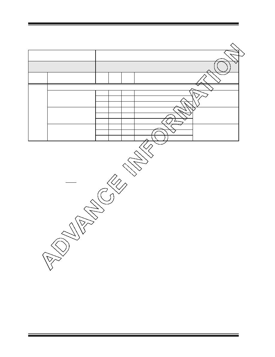
PIC18F2450/4450
DS39760A-page 268
Advance Information
� 2006 Microchip Technology Inc.
21.2
DC Characteristics:
Power-Down and Supply Current
PIC18F2450/4450 (Industrial)
PIC18LF2450/4450 (Industrial)
PIC18LF2450/4450
(Industrial)
Standard Operating Conditions (unless otherwise stated)
Operating temperature
-40�C
T
A
+85�C for industrial
PIC18F2450/4450
(Industrial)
Standard Operating Conditions (unless otherwise stated)
Operating temperature
-40�C
T
A
+85�C for industrial
Param
No.
Device
Typ
Max
Units
Conditions
Power-Down Current (I
PD
)
(1)
PIC18F2450/4450
0.1
TBD
A
-40�C
V
DD
= 2.0V
(Sleep mode)
0.1
TBD
A
+25�C
0.2
TBD
A
+85�C
PIC18LF2450/4450
0.1
TBD
A
-40�C
V
DD
= 3.0V
(Sleep mode)
0.1
TBD
A
+25�C
0.3
TBD
A
+85�C
All devices
0.1
TBD
A
-40�C
V
DD
= 5.0V
(Sleep mode)
0.1
TBD
A
+25�C
0.4
TBD
A
+85�C
Legend:
TBD = To Be Determined. Shading of rows is to assist in readability of the table.
Note 1:
The power-down current in Sleep mode does not depend on the oscillator type. Power-down current is measured
with the part in Sleep mode, with all I/O pins in high-impedance state and tied to V
DD
or V
SS
and all features that
add delta current disabled (such as WDT, Timer1 Oscillator, BOR, etc.).
2:
The supply current is mainly a function of operating voltage, frequency and mode. Other factors, such as I/O pin
loading and switching rate, oscillator type and circuit, internal code execution pattern and temperature, also have
an impact on the current consumption.
The test conditions for all I
DD
measurements in active operation mode are:
OSC1 = external square wave, from rail-to-rail; all I/O pins tri-stated, pulled to V
DD
or V
SS
;
MCLR = V
DD
; WDT enabled/disabled as specified.
3:
Standard low-cost 32 kHz crystals have an operating temperature range of -10�C to +70�C. Extended
temperature crystals are available at a much higher cost.
4:
BOR and HLVD enable internal band gap reference. With both modules enabled, current consumption will be
less than the sum of both specifications.
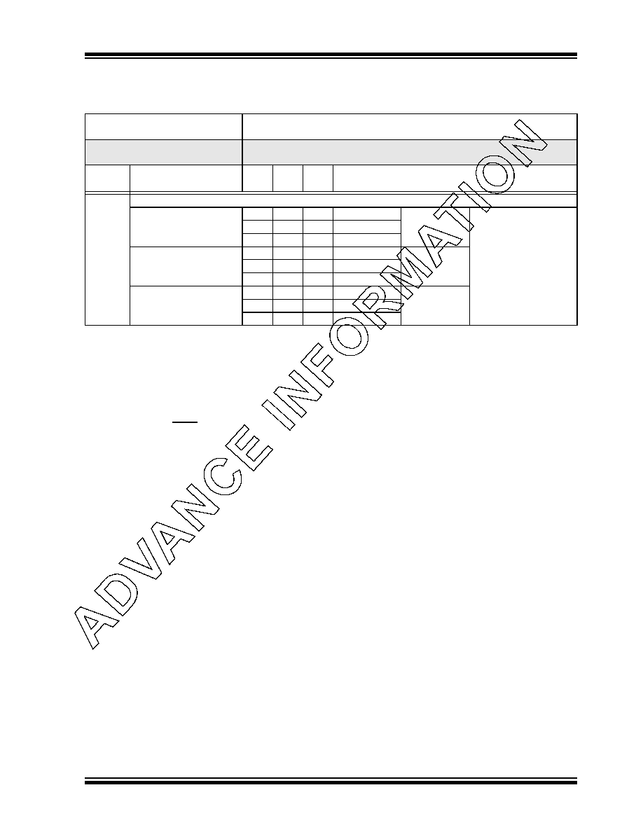
PIC18F2450/4450
� 2006 Microchip Technology Inc.
Advance Information
DS39760A-page 269
Supply Current (I
DD
)
(2)
PIC18LF2450/4450
15
TBD
A
-40�C
V
DD
= 2.0V
F
OSC
= 31 kHz
(RC_RUN mode,
INTRC source)
15
TBD
A
+25�C
15
TBD
A
+85�C
PIC18LF2450/4450
40
TBD
A
-40�C
V
DD
= 3.0V
35
TBD
A
+25�C
30
TBD
A
+85�C
All devices
105
TBD
A
-40�C
V
DD
= 5.0V
90
TBD
A
+25�C
80
TBD
A
+85�C
21.2
DC Characteristics:
Power-Down and Supply Current
PIC18F2450/4450 (Industrial)
PIC18LF2450/4450 (Industrial) (Continued)
PIC18LF2450/4450
(Industrial)
Standard Operating Conditions (unless otherwise stated)
Operating temperature
-40�C
T
A
+85�C for industrial
PIC18F2450/4450
(Industrial)
Standard Operating Conditions (unless otherwise stated)
Operating temperature
-40�C
T
A
+85�C for industrial
Param
No.
Device
Typ
Max
Units
Conditions
Legend:
TBD = To Be Determined. Shading of rows is to assist in readability of the table.
Note 1:
The power-down current in Sleep mode does not depend on the oscillator type. Power-down current is measured
with the part in Sleep mode, with all I/O pins in high-impedance state and tied to V
DD
or V
SS
and all features that
add delta current disabled (such as WDT, Timer1 Oscillator, BOR, etc.).
2:
The supply current is mainly a function of operating voltage, frequency and mode. Other factors, such as I/O pin
loading and switching rate, oscillator type and circuit, internal code execution pattern and temperature, also have
an impact on the current consumption.
The test conditions for all I
DD
measurements in active operation mode are:
OSC1 = external square wave, from rail-to-rail; all I/O pins tri-stated, pulled to V
DD
or V
SS
;
MCLR = V
DD
; WDT enabled/disabled as specified.
3:
Standard low-cost 32 kHz crystals have an operating temperature range of -10�C to +70�C. Extended
temperature crystals are available at a much higher cost.
4:
BOR and HLVD enable internal band gap reference. With both modules enabled, current consumption will be
less than the sum of both specifications.
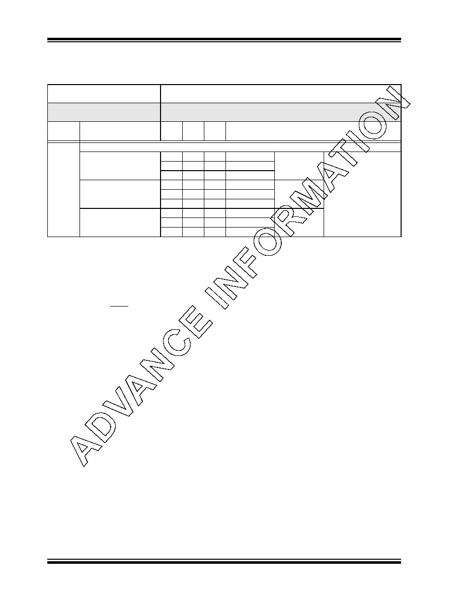
PIC18F2450/4450
DS39760A-page 270
Advance Information
� 2006 Microchip Technology Inc.
Supply Current (I
DD
)
(2)
PIC18LF2450/4450
2.9
TBD
A
-40�C
V
DD
= 2.0V
F
OSC
= 31 kHz
(RC_IDLE mode,
INTRC source)
3.1
TBD
A
+25�C
3.6
TBD
A
+85�C
PIC18LF2450/4450
4.5
TBD
A
-40�C
V
DD
= 3.0V
4.8
TBD
A
+25�C
5.8
TBD
A
+85�C
All devices
9.2
TBD
A
-40�C
V
DD
= 5.0V
9.8
TBD
A
+25�C
11.4
TBD
A
+85�C
21.2
DC Characteristics:
Power-Down and Supply Current
PIC18F2450/4450 (Industrial)
PIC18LF2450/4450 (Industrial) (Continued)
PIC18LF2450/4450
(Industrial)
Standard Operating Conditions (unless otherwise stated)
Operating temperature
-40�C
T
A
+85�C for industrial
PIC18F2450/4450
(Industrial)
Standard Operating Conditions (unless otherwise stated)
Operating temperature
-40�C
T
A
+85�C for industrial
Param
No.
Device
Typ
Max
Units
Conditions
Legend:
TBD = To Be Determined. Shading of rows is to assist in readability of the table.
Note 1:
The power-down current in Sleep mode does not depend on the oscillator type. Power-down current is measured
with the part in Sleep mode, with all I/O pins in high-impedance state and tied to V
DD
or V
SS
and all features that
add delta current disabled (such as WDT, Timer1 Oscillator, BOR, etc.).
2:
The supply current is mainly a function of operating voltage, frequency and mode. Other factors, such as I/O pin
loading and switching rate, oscillator type and circuit, internal code execution pattern and temperature, also have
an impact on the current consumption.
The test conditions for all I
DD
measurements in active operation mode are:
OSC1 = external square wave, from rail-to-rail; all I/O pins tri-stated, pulled to V
DD
or V
SS
;
MCLR = V
DD
; WDT enabled/disabled as specified.
3:
Standard low-cost 32 kHz crystals have an operating temperature range of -10�C to +70�C. Extended
temperature crystals are available at a much higher cost.
4:
BOR and HLVD enable internal band gap reference. With both modules enabled, current consumption will be
less than the sum of both specifications.
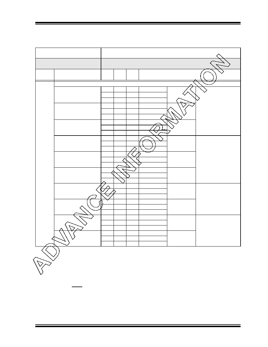
PIC18F2450/4450
� 2006 Microchip Technology Inc.
Advance Information
DS39760A-page 271
Supply Current (I
DD
)
(2)
PIC18LF2450/4450
250
TBD
A
-40�C
V
DD
= 2.0V
F
OSC
= 1 MH
Z
(PRI_RUN,
EC oscillator)
250
TBD
A
+25�C
250
TBD
A
+85�C
PIC18LF2450/4450
550
TBD
A
-40�C
V
DD
= 3.0V
480
TBD
A
+25�C
460
TBD
A
+85�C
All devices
1.2
TBD
mA
-40�C
V
DD
= 5.0V
1.1
TBD
mA
+25�C
1.0
TBD
mA
+85�C
PIC18LF2450/4450
0.74
TBD
mA
-40�C
V
DD
= 2.0V
F
OSC
= 4 MHz
(PRI_RUN,
EC oscillator)
0.74
TBD
mA
+25�C
0.74
TBD
mA
+85�C
PIC18LF2450/4450
1.3
TBD
mA
-40�C
V
DD
= 3.0V
1.3
TBD
mA
+25�C
1.3
TBD
mA
+85�C
All devices
2.7
TBD
mA
-40�C
V
DD
= 5.0V
2.6
TBD
mA
+25�C
2.5
TBD
mA
+85�C
All devices
15
TBD
mA
-40�C
V
DD
= 4.2V
F
OSC
= 40 MH
Z
(PRI_RUN,
EC oscillator)
16
TBD
mA
+25�C
16
TBD
mA
+85�C
All devices
21
TBD
mA
-40�C
V
DD
= 5.0V
21
TBD
mA
+25�C
21
TBD
mA
+85�C
All devices
20
TBD
mA
-40�C
V
DD
= 4.2V
F
OSC
= 48 MH
Z
(PRI_RUN,
EC oscillator)
20
TBD
mA
+25�C
20
TBD
mA
+85�C
All devices
25
TBD
mA
-40�C
V
DD
= 5.0V
25
TBD
mA
+25�C
25
TBD
mA
+85�C
21.2
DC Characteristics:
Power-Down and Supply Current
PIC18F2450/4450 (Industrial)
PIC18LF2450/4450 (Industrial) (Continued)
PIC18LF2450/4450
(Industrial)
Standard Operating Conditions (unless otherwise stated)
Operating temperature
-40�C
T
A
+85�C for industrial
PIC18F2450/4450
(Industrial)
Standard Operating Conditions (unless otherwise stated)
Operating temperature
-40�C
T
A
+85�C for industrial
Param
No.
Device
Typ
Max
Units
Conditions
Legend:
TBD = To Be Determined. Shading of rows is to assist in readability of the table.
Note 1:
The power-down current in Sleep mode does not depend on the oscillator type. Power-down current is measured
with the part in Sleep mode, with all I/O pins in high-impedance state and tied to V
DD
or V
SS
and all features that
add delta current disabled (such as WDT, Timer1 Oscillator, BOR, etc.).
2:
The supply current is mainly a function of operating voltage, frequency and mode. Other factors, such as I/O pin
loading and switching rate, oscillator type and circuit, internal code execution pattern and temperature, also have
an impact on the current consumption.
The test conditions for all I
DD
measurements in active operation mode are:
OSC1 = external square wave, from rail-to-rail; all I/O pins tri-stated, pulled to V
DD
or V
SS
;
MCLR = V
DD
; WDT enabled/disabled as specified.
3:
Standard low-cost 32 kHz crystals have an operating temperature range of -10�C to +70�C. Extended
temperature crystals are available at a much higher cost.
4:
BOR and HLVD enable internal band gap reference. With both modules enabled, current consumption will be
less than the sum of both specifications.
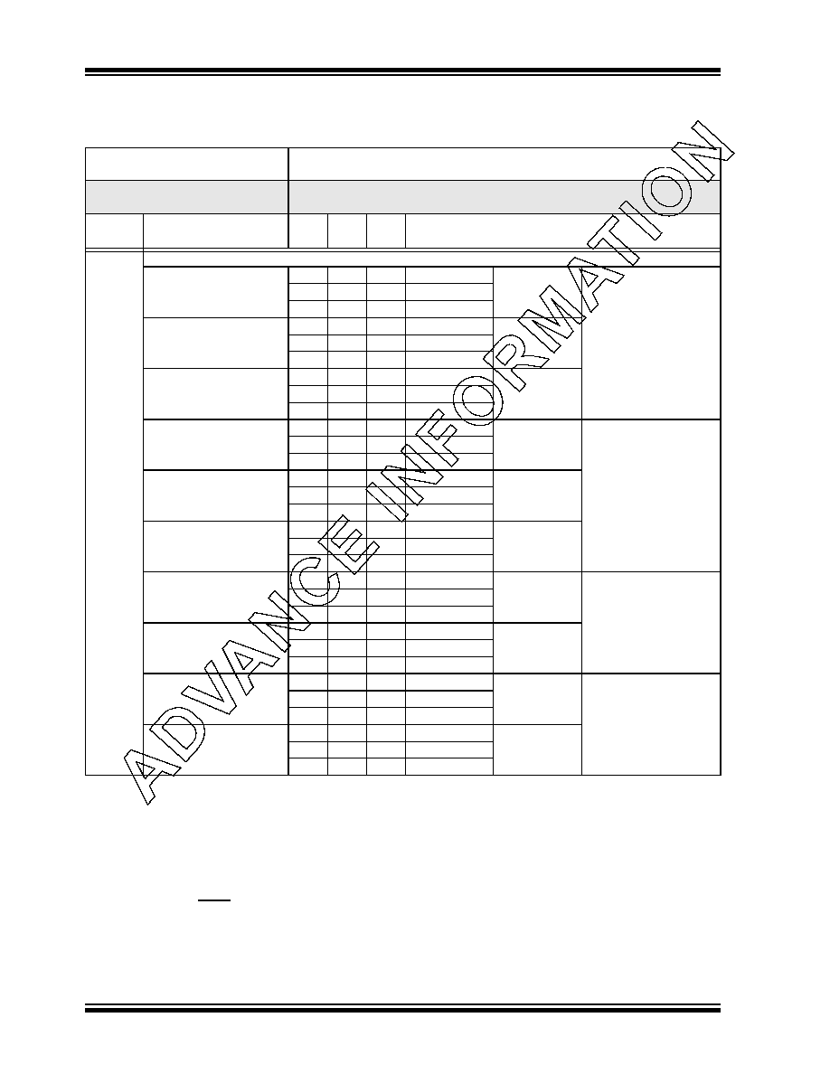
PIC18F2450/4450
DS39760A-page 272
Advance Information
� 2006 Microchip Technology Inc.
Supply Current (I
DD
)
(2)
PIC18LF2450/4450
65
TBD
A
-40�C
V
DD
= 2.0V
F
OSC
= 1 MHz
(PRI_IDLE mode,
EC oscillator)
65
TBD
A
+25�C
70
TBD
A
+85�C
PIC18LF2450/4450
120
TBD
A
-40�C
V
DD
= 3.0V
120
TBD
A
+25�C
130
TBD
A
+85�C
All devices
230
TBD
A
-40�C
V
DD
= 5.0V
240
TBD
A
+25�C
250
TBD
A
+85�C
PIC18LF2450/4450
255
TBD
A
-40�C
V
DD
= 2.0V
F
OSC
= 4 MHz
(PRI_IDLE mode,
EC oscillator)
260
TBD
A
+25�C
270
TBD
A
+85�C
PIC18LF2450/4450
420
TBD
A
-40�C
V
DD
= 3.0V
430
TBD
A
+25�C
450
TBD
A
+85�C
All devices
0.9
TBD
mA
-40�C
V
DD
= 5.0V
0.9
TBD
mA
+25�C
0.9
TBD
mA
+85�C
All devices
6.0
TBD
mA
-40�C
V
DD
= 4.2V
F
OSC
= 40 MHz
(PRI_IDLE mode,
EC oscillator)
6.2
TBD
mA
+25�C
6.6
TBD
mA
+85�C
All devices
8.1
TBD
mA
-40�C
V
DD
= 5.0V
8.3
TBD
mA
+25�C
9.0
TBD
mA
+85�C
All devices
8.0
TBD
mA
-40�C
V
DD
= 4.2V
F
OSC
= 48 MHz
(PRI_IDLE mode,
EC oscillator)
8.1
TBD
mA
+25�C
8.2
TBD
mA
+85�C
All devices
9.8
TBD
mA
-40�C
V
DD
= 5.0V
10.0
TBD
mA
+25�C
10.5
TBD
mA
+85�C
21.2
DC Characteristics:
Power-Down and Supply Current
PIC18F2450/4450 (Industrial)
PIC18LF2450/4450 (Industrial) (Continued)
PIC18LF2450/4450
(Industrial)
Standard Operating Conditions (unless otherwise stated)
Operating temperature
-40�C
T
A
+85�C for industrial
PIC18F2450/4450
(Industrial)
Standard Operating Conditions (unless otherwise stated)
Operating temperature
-40�C
T
A
+85�C for industrial
Param
No.
Device
Typ
Max
Units
Conditions
Legend:
TBD = To Be Determined. Shading of rows is to assist in readability of the table.
Note 1:
The power-down current in Sleep mode does not depend on the oscillator type. Power-down current is measured
with the part in Sleep mode, with all I/O pins in high-impedance state and tied to V
DD
or V
SS
and all features that
add delta current disabled (such as WDT, Timer1 Oscillator, BOR, etc.).
2:
The supply current is mainly a function of operating voltage, frequency and mode. Other factors, such as I/O pin
loading and switching rate, oscillator type and circuit, internal code execution pattern and temperature, also have
an impact on the current consumption.
The test conditions for all I
DD
measurements in active operation mode are:
OSC1 = external square wave, from rail-to-rail; all I/O pins tri-stated, pulled to V
DD
or V
SS
;
MCLR = V
DD
; WDT enabled/disabled as specified.
3:
Standard low-cost 32 kHz crystals have an operating temperature range of -10�C to +70�C. Extended
temperature crystals are available at a much higher cost.
4:
BOR and HLVD enable internal band gap reference. With both modules enabled, current consumption will be
less than the sum of both specifications.
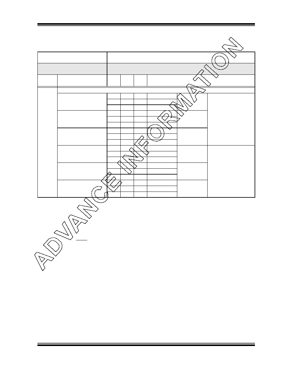
PIC18F2450/4450
� 2006 Microchip Technology Inc.
Advance Information
DS39760A-page 273
Supply Current (I
DD
)
(2)
PIC18LF2450/4450
14
TBD
A
-40�C
V
DD
= 2.0V
F
OSC
= 32 kHz
(3)
(SEC_RUN mode,
Timer1 as clock)
15
TBD
A
+25�C
16
TBD
A
+85�C
PIC18LF2450/4450
40
TBD
A
-40�C
V
DD
= 3.0V
35
TBD
A
+25�C
31
TBD
A
+85�C
All devices
99
TBD
A
-40�C
V
DD
= 5.0V
81
TBD
A
+25�C
75
TBD
A
+85�C
PIC18LF2450/4450
2.5
TBD
A
-40�C
V
DD
= 2.0V
F
OSC
= 32 kHz
(3)
(SEC_IDLE mode,
Timer1 as clock)
3.7
TBD
A
+25�C
4.5
TBD
A
+85�C
PIC18LF2450/4450
5.0
TBD
A
-40�C
V
DD
= 3.0V
5.4
TBD
A
+25�C
6.3
TBD
A
+85�C
All devices
8.5
TBD
A
-40�C
V
DD
= 5.0V
9.0
TBD
A
+25�C
10.5
TBD
A
+85�C
21.2
DC Characteristics:
Power-Down and Supply Current
PIC18F2450/4450 (Industrial)
PIC18LF2450/4450 (Industrial) (Continued)
PIC18LF2450/4450
(Industrial)
Standard Operating Conditions (unless otherwise stated)
Operating temperature
-40�C
T
A
+85�C for industrial
PIC18F2450/4450
(Industrial)
Standard Operating Conditions (unless otherwise stated)
Operating temperature
-40�C
T
A
+85�C for industrial
Param
No.
Device
Typ
Max
Units
Conditions
Legend:
TBD = To Be Determined. Shading of rows is to assist in readability of the table.
Note 1:
The power-down current in Sleep mode does not depend on the oscillator type. Power-down current is measured
with the part in Sleep mode, with all I/O pins in high-impedance state and tied to V
DD
or V
SS
and all features that
add delta current disabled (such as WDT, Timer1 Oscillator, BOR, etc.).
2:
The supply current is mainly a function of operating voltage, frequency and mode. Other factors, such as I/O pin
loading and switching rate, oscillator type and circuit, internal code execution pattern and temperature, also have
an impact on the current consumption.
The test conditions for all I
DD
measurements in active operation mode are:
OSC1 = external square wave, from rail-to-rail; all I/O pins tri-stated, pulled to V
DD
or V
SS
;
MCLR = V
DD
; WDT enabled/disabled as specified.
3:
Standard low-cost 32 kHz crystals have an operating temperature range of -10�C to +70�C. Extended
temperature crystals are available at a much higher cost.
4:
BOR and HLVD enable internal band gap reference. With both modules enabled, current consumption will be
less than the sum of both specifications.
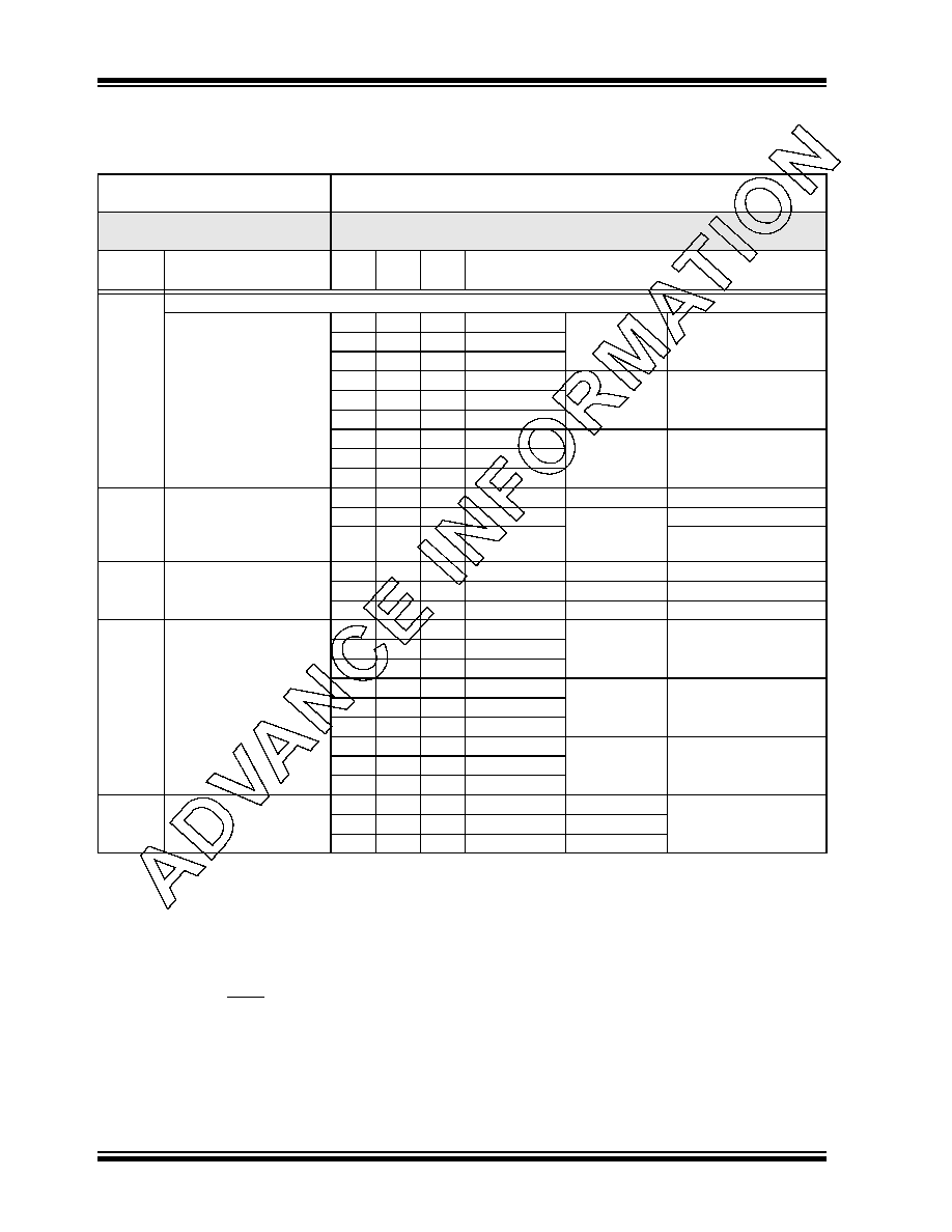
PIC18F2450/4450
DS39760A-page 274
Advance Information
� 2006 Microchip Technology Inc.
D022
(
I
WDT
)
Module Differential Currents (
I
WDT
,
I
BOR
,
I
LVD
,
I
OSCB
,
I
AD
)
Watchdog Timer
1.3
TBD
A
-40�C
V
DD
= 2.0V
1.4
TBD
A
+25�C
2.0
TBD
A
+85�C
1.9
TBD
A
-40�C
V
DD
= 3.0V
2.0
TBD
A
+25�C
2.8
TBD
A
+85�C
4.0
TBD
A
-40�C
V
DD
= 5.0V
5.5
TBD
A
+25�C
5.6
TBD
A
+85�C
D022A
(
I
BOR
)
Brown-out Reset
(4)
35
TBD
A
-40�C to +85�C
V
DD
= 3.0V
40
TBD
A
-40�C to +85�C
V
DD
= 5.0V
0
TBD
A
-40�C to +85�C
Sleep mode,
BOREN1:BOREN0 = 10
D022B
(
I
LVD
)
High/Low-Voltage
Detect
(4)
22
TBD
A
-40�C to +85�C
V
DD
= 2.0V
25
TBD
A
-40�C to +85�C
V
DD
= 3.0V
29
TBD
A
-40�C to +85�C
V
DD
= 5.0V
D025
(
I
OSCB
)
Timer1 Oscillator
2.1
TBD
A
-40�C
V
DD
= 2.0V
32 kHz on Timer1
(3)
1.8
TBD
A
+25�C
2.1
TBD
A
+85�C
2.2
TBD
A
-40�C
V
DD
= 3.0V
32 kHz on Timer1
(3)
2.6
TBD
A
+25�C
2.9
TBD
A
+85�C
3.0
TBD
A
-40�C
V
DD
= 5.0V
32 kHz on Timer1
(3)
3.2
TBD
A
+25�C
3.4
TBD
A
+85�C
D026
(
I
AD
)
A/D Converter
1.0
TBD
A
-40�C to +85�C
V
DD
= 2.0V
A/D on, not converting
1.0
TBD
A
-40�C to +85�C
V
DD
= 3.0V
1.0
TBD
A
-40�C to +85�C
V
DD
= 5.0V
21.2
DC Characteristics:
Power-Down and Supply Current
PIC18F2450/4450 (Industrial)
PIC18LF2450/4450 (Industrial) (Continued)
PIC18LF2450/4450
(Industrial)
Standard Operating Conditions (unless otherwise stated)
Operating temperature
-40�C
T
A
+85�C for industrial
PIC18F2450/4450
(Industrial)
Standard Operating Conditions (unless otherwise stated)
Operating temperature
-40�C
T
A
+85�C for industrial
Param
No.
Device
Typ
Max
Units
Conditions
Legend:
TBD = To Be Determined. Shading of rows is to assist in readability of the table.
Note 1:
The power-down current in Sleep mode does not depend on the oscillator type. Power-down current is measured
with the part in Sleep mode, with all I/O pins in high-impedance state and tied to V
DD
or V
SS
and all features that
add delta current disabled (such as WDT, Timer1 Oscillator, BOR, etc.).
2:
The supply current is mainly a function of operating voltage, frequency and mode. Other factors, such as I/O pin
loading and switching rate, oscillator type and circuit, internal code execution pattern and temperature, also have
an impact on the current consumption.
The test conditions for all I
DD
measurements in active operation mode are:
OSC1 = external square wave, from rail-to-rail; all I/O pins tri-stated, pulled to V
DD
or V
SS
;
MCLR = V
DD
; WDT enabled/disabled as specified.
3:
Standard low-cost 32 kHz crystals have an operating temperature range of -10�C to +70�C. Extended
temperature crystals are available at a much higher cost.
4:
BOR and HLVD enable internal band gap reference. With both modules enabled, current consumption will be
less than the sum of both specifications.
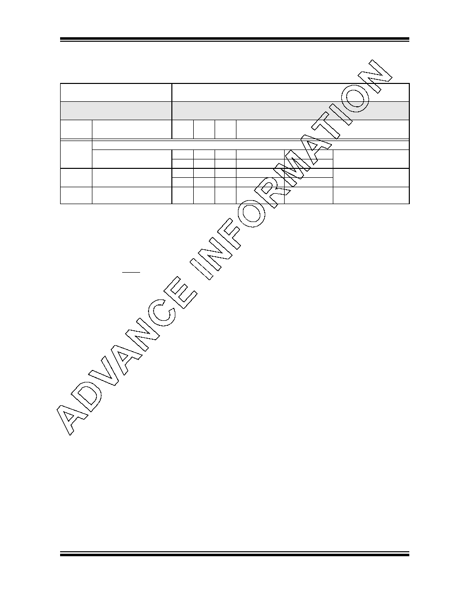
PIC18F2450/4450
� 2006 Microchip Technology Inc.
Advance Information
DS39760A-page 275
USB and Related Module Differential Currents (
I
USB
x,
I
PLL
,
I
UREG
)
I
USB
x
USB Module
with On-Chip Transceiver
TBD
TBD
mA
+25
�C
V
DD
= 3.3V
TBD
TBD
mA
+25
�C
V
DD
= 5.0V
I
PLL
96 MHz PLL
(Oscillator Module)
TBD
TBD
TBD
+25
�C
V
DD
= 3.3V
TBD
TBD
TBD
+25
�C
V
DD
= 5.0V
I
UREG
USB Internal Voltage
Regulator
TBD
TBD
TBD
+25
�C
V
DD
= 5.0V
21.2
DC Characteristics:
Power-Down and Supply Current
PIC18F2450/4450 (Industrial)
PIC18LF2450/4450 (Industrial) (Continued)
PIC18LF2450/4450
(Industrial)
Standard Operating Conditions (unless otherwise stated)
Operating temperature
-40�C
T
A
+85�C for industrial
PIC18F2450/4450
(Industrial)
Standard Operating Conditions (unless otherwise stated)
Operating temperature
-40�C
T
A
+85�C for industrial
Param
No.
Device
Typ
Max
Units
Conditions
Legend:
TBD = To Be Determined. Shading of rows is to assist in readability of the table.
Note 1:
The power-down current in Sleep mode does not depend on the oscillator type. Power-down current is measured
with the part in Sleep mode, with all I/O pins in high-impedance state and tied to V
DD
or V
SS
and all features that
add delta current disabled (such as WDT, Timer1 Oscillator, BOR, etc.).
2:
The supply current is mainly a function of operating voltage, frequency and mode. Other factors, such as I/O pin
loading and switching rate, oscillator type and circuit, internal code execution pattern and temperature, also have
an impact on the current consumption.
The test conditions for all I
DD
measurements in active operation mode are:
OSC1 = external square wave, from rail-to-rail; all I/O pins tri-stated, pulled to V
DD
or V
SS
;
MCLR = V
DD
; WDT enabled/disabled as specified.
3:
Standard low-cost 32 kHz crystals have an operating temperature range of -10�C to +70�C. Extended
temperature crystals are available at a much higher cost.
4:
BOR and HLVD enable internal band gap reference. With both modules enabled, current consumption will be
less than the sum of both specifications.

PIC18F2450/4450
DS39760A-page 276
Advance Information
� 2006 Microchip Technology Inc.
21.3
DC Characteristics: PIC18F2450/4450 (Industrial)
PIC18LF2450/4450 (Industrial)
DC CHARACTERISTICS
Standard Operating Conditions (unless otherwise stated)
Operating temperature -40�C
T
A
+85�C for industrial
Param
No.
Sym
Characteristic
Min
Max
Units
Conditions
V
IL
Input Low Voltage
I/O Ports (except RC4/RC5 in
USB mode):
D030
with TTL buffer
V
SS
0.15 V
DD
V
V
DD
< 4.5V
D030A
--
0.8
V
4.5V
V
DD
5.5V
D031
with Schmitt Trigger buffer
RC3 and RC4
V
SS
V
SS
0.2 V
DD
0.3 V
DD
V
V
D032
MCLR
V
SS
0.2 V
DD
V
D032A
OSC1 and T1OSI
V
SS
0.3 V
DD
V
XT, HS, HSPLL modes
(1)
D033
OSC1 V
SS
0.2 V
DD
V
EC mode
(1)
V
ILU
D+/D- Input
--
0.8
V
V
DD
= 4.35V,
USB suspended
(5)
V
IH
Input High Voltage
I/O Ports (except RC4/RC5 in
USB mode):
D040
with TTL buffer
0.25 V
DD
+ 0.8V
V
DD
V
V
DD
< 4.5V
D040A
2.0
V
DD
V
4.5V
V
DD
5.5V
D041
with Schmitt Trigger buffer
RC3 and RC4
0.8 V
DD
0.7 V
DD
V
DD
V
DD
V
V
D042
MCLR
0.8 V
DD
V
DD
V
D042A
OSC1 and T1OSI
0.7 V
DD
V
DD
V
XT, HS, HSPLL modes
(1)
D043
OSC1 0.8
V
DD
V
DD
V
EC mode
(1)
V
IHU
D+/D- Input
2.4
--
V
V
DD
= 4.35V,
USB suspended
(5)
I
IL
Input Leakage Current
(2,3)
D060
I/O Ports
--
�1
A V
SS
V
PIN
V
DD
,
Pin at high-impedance
D061
MCLR
--
�5
A Vss V
PIN
V
DD
D063
OSC1
--
�5
A Vss V
PIN
V
DD
I
PU
Weak Pull-up Current
D070
I
PURB
PORTB Weak Pull-up Current
50
400
A V
DD
= 5V, V
PIN
= V
SS
Note 1:
In RC oscillator configuration, the OSC1/CLKI pin is a Schmitt Trigger input. It is not recommended that the
PICmicro
�
device be driven with an external clock while in RC mode.
2:
The leakage current on the MCLR pin is strongly dependent on the applied voltage level. The specified
levels represent normal operating conditions. Higher leakage current may be measured at different input
voltages.
3:
Negative current is defined as current sourced by the pin.
4:
Parameter is characterized but not tested.
5:
D+ parameters per USB Specification 2.0.

PIC18F2450/4450
� 2006 Microchip Technology Inc.
Advance Information
DS39760A-page 277
V
OL
Output Low Voltage
D080
I/O Ports (except RC4/RC5 in
USB mode)
--
0.6
V
I
OL
= 8.5 mA, V
DD
= 4.5V,
-40
�C to +85�C
D083
OSC2/CLKO
(EC, ECIO modes)
--
0.6
V
I
OL
= 1.6 mA, V
DD
= 4.5V,
-40
�C to +85�C
V
OLU
D+/D- Out
--
0.3
V
DD
= 4.35V,
USB suspended
(5)
V
OH
Output High Voltage
(3)
D090
I/O Ports (except RC4/RC5 in
USB mode)
V
DD
� 0.7
--
V
I
OH
= -3.0 mA, V
DD
= 4.5V,
-40
�C to +85�C
D092
OSC2/CLKO
(EC, ECIO, ECPIO modes)
V
DD
� 0.7
--
V
I
OH
= -1.3 mA, V
DD
= 4.5V,
-40
�C to +85�C
V
OHU
D+/D- Out
2.8
3.6
V
V
DD
= 4.35V,
USB suspended
(5)
Capacitive Loading Specs
on Output Pins
D100
(4)
C
OSC
2
OSC2 pin
--
15
pF
In XT and HS modes
when external clock is
used to drive OSC1
D101
C
IO
All I/O pins and OSC2
(in RC mode)
--
50
pF
To meet the AC Timing
Specifications
21.3
DC Characteristics: PIC18F2450/4450 (Industrial)
PIC18LF2450/4450 (Industrial) (Continued)
DC CHARACTERISTICS
Standard Operating Conditions (unless otherwise stated)
Operating temperature -40�C
T
A
+85�C for industrial
Param
No.
Sym
Characteristic
Min
Max
Units
Conditions
Note 1:
In RC oscillator configuration, the OSC1/CLKI pin is a Schmitt Trigger input. It is not recommended that the
PICmicro
�
device be driven with an external clock while in RC mode.
2:
The leakage current on the MCLR pin is strongly dependent on the applied voltage level. The specified
levels represent normal operating conditions. Higher leakage current may be measured at different input
voltages.
3:
Negative current is defined as current sourced by the pin.
4:
Parameter is characterized but not tested.
5:
D+ parameters per USB Specification 2.0.

PIC18F2450/4450
DS39760A-page 278
Advance Information
� 2006 Microchip Technology Inc.
TABLE 21-1:
MEMORY PROGRAMMING REQUIREMENTS
DC Characteristics
Standard Operating Conditions (unless otherwise stated)
Operating temperature
-40�C
T
A
+85�C for industrial
Param
No.
Sym
Characteristic
Min
Typ
Max
Units
Conditions
Internal Program Memory
Programming Specifications
(1)
D110
V
PP
Voltage on MCLR/V
PP
/RE3 pin
9.00
--
13.25
V
(Note 2)
D113
I
DDP
Supply Current during
Programming
--
--
10
mA
Program Flash Memory
D130
E
P
Cell Endurance
10K
100K
--
E/W
-40
�C to +85�C
D131
V
PR
V
DD
for Read
V
MIN
--
5.5
V
V
MIN
= Minimum operating
voltage
D132
V
IE
V
DD
for Block Erase
4.5
--
5.5
V
Using ICSPTM port
D132A V
IW
V
DD
for Externally Timed Erase
or Write
3.0
--
5.5
V
Using ICSP port
D132B V
PEW
V
DD
for Self-Timed Write
V
MIN
--
5.5
V
V
MIN
= Minimum operating
voltage
D133
T
IE
ICSP Block Erase Cycle Time
--
4
--
ms
V
DD
> 4.5V
D133A T
IW
ICSP Erase or Write Cycle Time
(externally timed)
1
--
--
ms
V
DD
> 4.5V
D133A T
IW
Self-Timed Write Cycle Time
--
2
--
ms
D134
T
RETD
Characteristic Retention
40
100
--
Year Provided no other
specifications are violated
Data in "Typ" column is at 5.0V, 25�C unless otherwise stated. These parameters are for design guidance
only and are not tested.
Note 1:
These specifications are for programming the on-chip program memory through the use of table write
instructions.
2:
Required only if Single-Supply Programming is disabled.
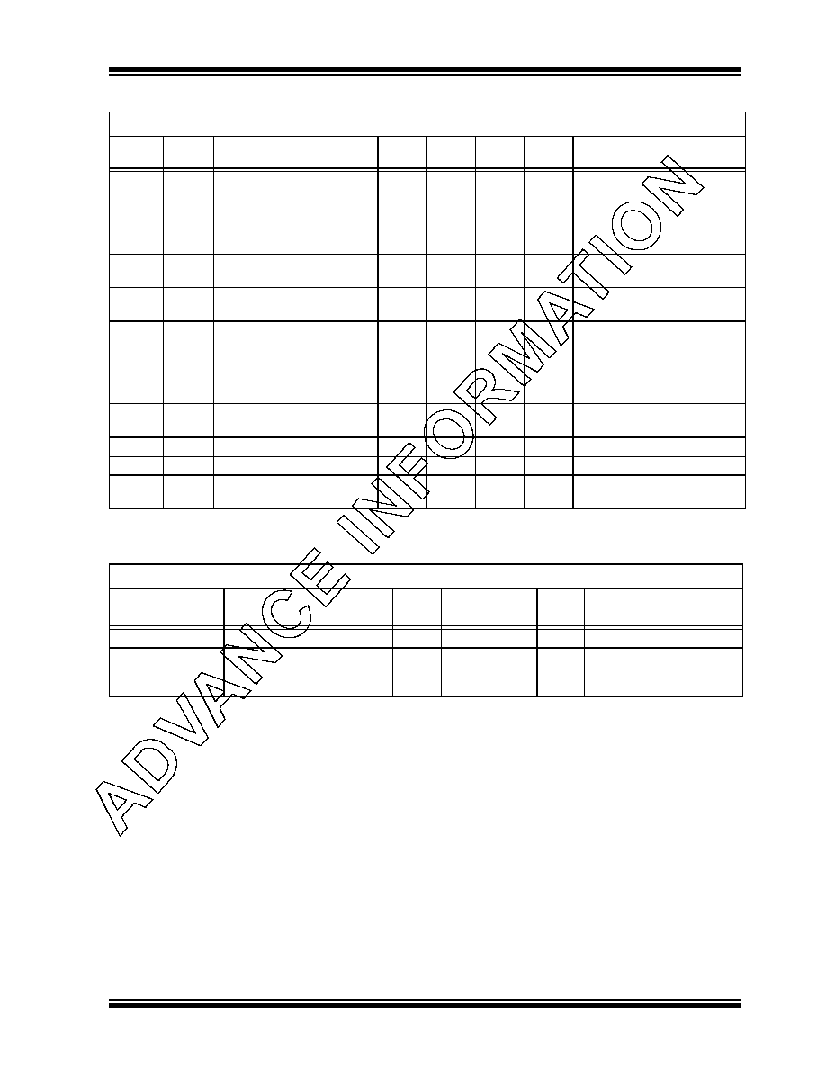
PIC18F2450/4450
� 2006 Microchip Technology Inc.
Advance Information
DS39760A-page 279
TABLE 21-2:
USB MODULE SPECIFICATIONS
TABLE 21-3:
USB INTERNAL VOLTAGE REGULATOR SPECIFICATIONS
Operating Conditions: -40�C < T
A
< +85�C (unless otherwise stated).
Param
No.
Sym
Characteristic
Min
Typ
Max
Units
Comments
D313
V
USB
USB Voltage
3.0
--
3.6
V
Voltage on bus must be in this
range for proper USB
operation
D314
I
IL
Input Leakage on pin
--
--
�1
A
V
SS
V
PAD
V
DD
;
pin at high impedance
D315
V
ILUSB
Input Low Voltage for USB
Buffer
--
--
0.8
V
For V
USB
range
D316
V
IHUSB
Input High Voltage for USB
Buffer
2.0
--
--
V
For V
USB
range
D317
V
CRS
Crossover Voltage
1.3
2.0
V
Voltage range for pad_dp and
pad_dm crossover to occur
D318
V
DIFS
Differential Input Sensitivity
--
--
0.2
V
The difference between D+
and D- must exceed this value
while V
CM
is met
D319
V
CM
Differential Common Mode
Range
0.8
--
2.5
V
D320
Z
OUT
Driver Output Impedance
28
--
44
D321
V
OL
Voltage Output Low
0.0
--
0.3
V
1.5 k
load connected to 3.6V
D322
V
OH
Voltage Output High
2.8
--
3.6
V
15 k
load connected to
ground
Operating Conditions: -40�C < T
A
< +85�C (unless otherwise stated).
Param
No.
Sym
Characteristics
Min
Typ Max
Units
Comments
D323
V
USBANA
Regulator Output Voltage*
3.0
--
3.6
V
D324
C
USB
External Filter Capacitor
Value*
220
--
--
nF
Must hold sufficient charge
for peak load with minimal
voltage drop
*
These parameters are characterized but not tested. Parameter numbers not yet assigned for these
specifications.
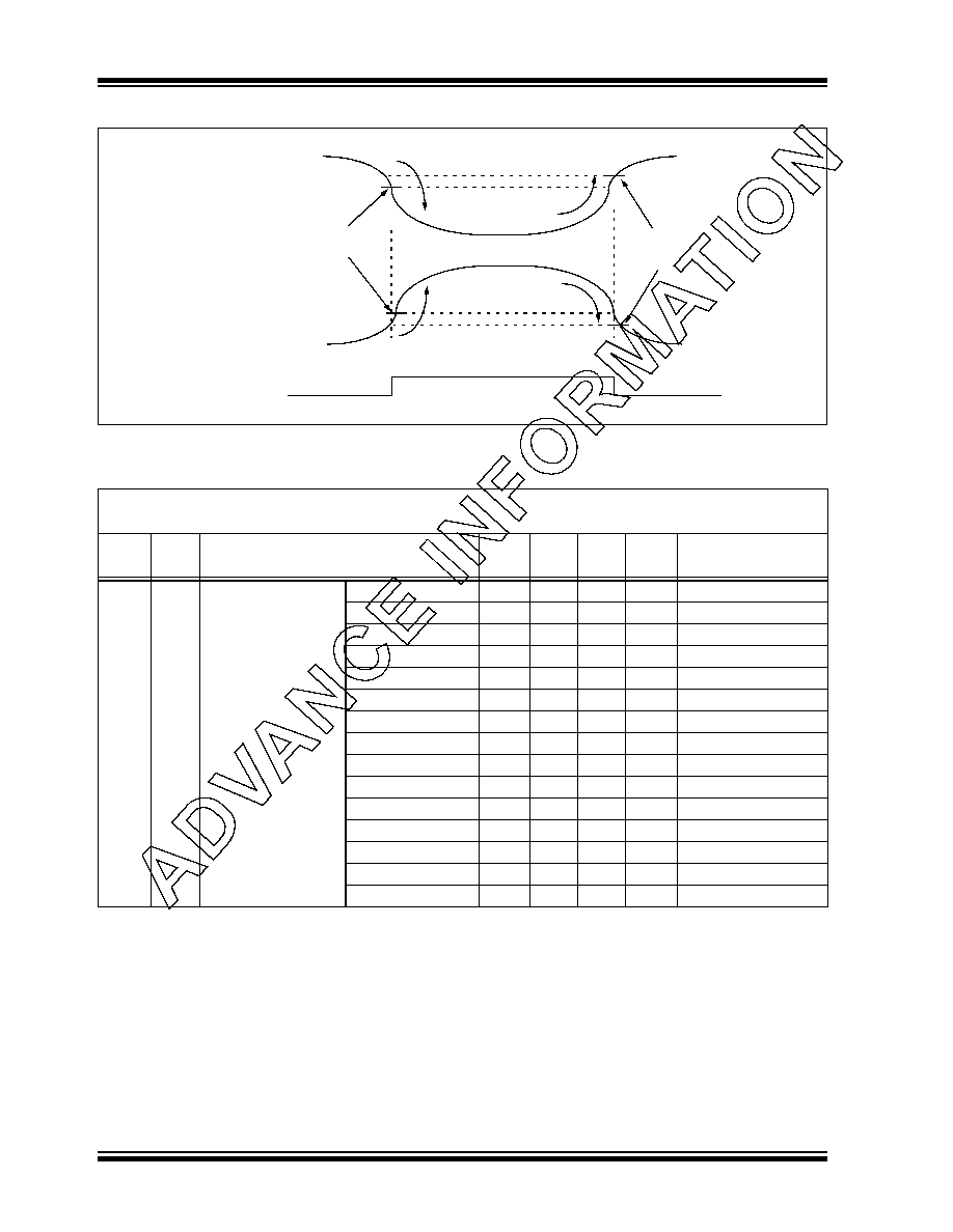
PIC18F2450/4450
DS39760A-page 280
Advance Information
� 2006 Microchip Technology Inc.
FIGURE 21-3:
HIGH/LOW-VOLTAGE DETECT CHARACTERISTICS
TABLE 21-4:
HIGH/LOW-VOLTAGE DETECT CHARACTERISTICS
V
HLVD
HLVDIF
V
DD
(HLVDIF set by hardware)
(HLVDIF can be
cleared in software)
V
HLVD
For VDIRMAG = 1:
For VDIRMAG = 0:
V
DD
Standard Operating Conditions (unless otherwise stated)
Operating temperature -40�C
T
A
+85�C for industrial
Param
No.
Sym
Characteristic
Min
Typ
Max
Units
Conditions
D420
HLVD Voltage on V
DD
Transition High-to-Low
HLVDL<3:0> = 0000
2.06
2.17
2.28
V
HLVDL<3:0> = 0001
2.12
2.23
2.34
V
HLVDL<3:0> = 0010
2.24
2.36
2.48
V
HLVDL<3:0> = 0011
2.32
2.44
2.56
V
HLVDL<3:0> = 0100
2.47
2.60
2.73
V
HLVDL<3:0> = 0101
2.65
2.79
2.93
V
HLVDL<3:0> = 0110
2.74
2.89
3.04
V
HLVDL<3:0> = 0111
2.96
3.12
3.28
V
HLVDL<3:0> = 1000
3.22
3.39
3.56
V
HLVDL<3:0> = 1001
3.37
3.55
3.73
V
HLVDL<3:0> = 1010
3.52
3.71
3.90
V
HLVDL<3:0> = 1011
3.70
3.90
4.10
V
HLVDL<3:0> = 1100
3.90
4.11
4.32
V
HLVDL<3:0> = 1101
4.11
4.33
4.55
V
HLVDL<3:0> = 1110
4.36
4.59
4.82
V

PIC18F2450/4450
� 2006 Microchip Technology Inc.
Advance Information
DS39760A-page 281
21.4
AC (Timing) Characteristics
21.4.1
TIMING PARAMETER SYMBOLOGY
The timing parameter symbols have been created
using one of the following formats:
1. TppS2ppS
2. TppS
T
F
Frequency
T
Time
Lowercase letters (pp) and their meanings:
pp
mc
MCLR
cc
CCP1
osc
OSC1
ck
CLKO
wr
WR
dt
Data in
t0
T0CKI
io
I/O port
t1
T1CKI
:Uppercase Letters and their meanings
S
F
Fall
P
Period
H
High
R
Rise
I
Invalid (High-Impedance)
V
Valid
L
Low
Z
High-Impedance
High
High
Low
Low
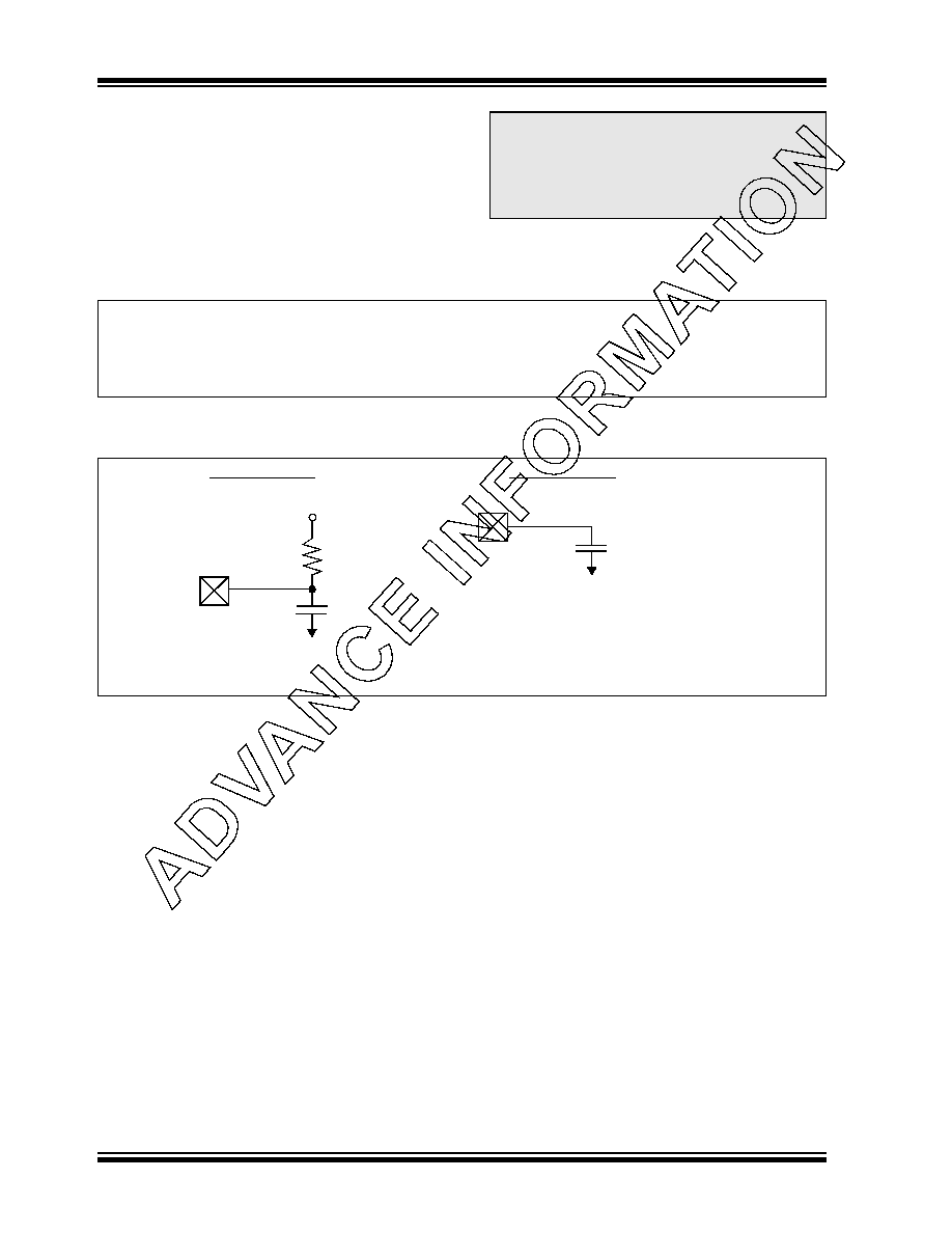
PIC18F2450/4450
DS39760A-page 282
Advance Information
� 2006 Microchip Technology Inc.
21.4.2
TIMING CONDITIONS
The temperature and voltages specified in Table 21-5
apply to all timing specifications unless otherwise
noted. Figure 21-4 specifies the load conditions for the
timing specifications.
TABLE 21-5:
TEMPERATURE AND VOLTAGE SPECIFICATIONS � AC
FIGURE 21-4:
LOAD CONDITIONS FOR DEVICE TIMING SPECIFICATIONS
Note:
Because of space limitations, the generic
terms "PIC18FXXXX" and "PIC18LFXXXX"
are used throughout this section to refer to
the PIC18F2450/4450 and PIC18LF2450/
4450 families of devices specifically and
only those devices.
AC CHARACTERISTICS
Standard Operating Conditions (unless otherwise stated)
Operating temperature
-40�C
T
A
+85�C for industrial
Operating voltage V
DD
range as described in DC spec Section 21.1 and
Section 21.3 .
LF parts operate for industrial temperatures only.
V
DD
/2
C
L
R
L
Pin
Pin
V
SS
V
SS
C
L
R
L
= 464
C
L
= 50 pF
for all pins except OSC2/CLKO
and including D and E outputs as ports
Load Condition 1
Load Condition 2
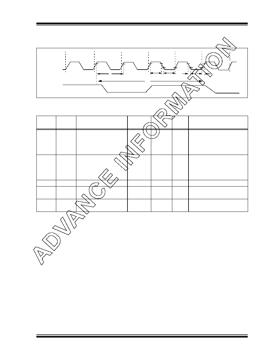
PIC18F2450/4450
� 2006 Microchip Technology Inc.
Advance Information
DS39760A-page 283
21.4.3
TIMING DIAGRAMS AND SPECIFICATIONS
FIGURE 21-5:
EXTERNAL CLOCK TIMING (ALL MODES EXCEPT PLL)
TABLE 21-6:
EXTERNAL CLOCK TIMING REQUIREMENTS
OSC1
CLKO
Q4
Q1
Q2
Q3
Q4
Q1
1
2
3
3
4
4
Param.
No.
Symbol
Characteristic
Min
Max
Units
Conditions
1A
F
OSC
External CLKI Frequency
(1)
Oscillator Frequency
(1)
DC
48
MHz
EC, ECIO Oscillator mode
0.1
4
MHz
XT, XTPLL Oscillator mode
4
25
MHz
HS Oscillator mode
4
48
MHz
HSPLL Oscillator mode
1
T
OSC
External CLKI Period
(1)
Oscillator Period
(1)
20.8
--
ns
EC, ECIO Oscillator mode
250
10,000
ns
XT Oscillator mode
25
20.8
250
250
ns
ns
HS Oscillator mode
HSPLL Oscillator mode
2
T
CY
Instruction Cycle Time
(1)
83.3
--
ns
T
CY
= 4/F
OSC
3
TosL,
TosH
External Clock in (OSC1)
High or Low Time
30
--
ns
XT Oscillator mode
10
--
ns
HS Oscillator mode
4
TosR,
TosF
External Clock in (OSC1)
Rise or Fall Time
--
20
ns
XT Oscillator mode
--
7.5
ns
HS Oscillator mode
Note 1:
Instruction cycle period (T
CY
) equals four times the input oscillator time base period for all configurations
except PLL. All specified values are based on characterization data for that particular oscillator type under
standard operating conditions with the device executing code. Exceeding these specified limits may result
in an unstable oscillator operation and/or higher than expected current consumption. All devices are tested
to operate at "min." values with an external clock applied to the OSC1/CLKI pin. When an external clock
input is used, the "max." cycle time limit is "DC" (no clock) for all devices.
PIC18F2450/4450
DS39760A-page 284
Advance Information
� 2006 Microchip Technology Inc.
TABLE 21-7:
PLL CLOCK TIMING SPECIFICATIONS (V
DD
= 4.2V TO 5.5V)
TABLE 21-8:
AC CHARACTERISTICS: INTERNAL RC ACCURACY
PIC18F2450/4450 (INDUSTRIAL)
PIC18LF2450/4450 (INDUSTRIAL)
FIGURE 21-6:
CLKO AND I/O TIMING
Param
No.
Sym
Characteristic
Min
Typ
Max
Units
Conditions
F10
F
OSC
Oscillator Frequency Range
4
--
48
MHz
F11
F
SYS
On-Chip VCO System Frequency
--
96
--
MHz
F12
t
rc
PLL Start-up Time (Lock Time)
--
--
2
ms
F13
CLK
CLKO Stability (Jitter)
-0.25
--
+0.25
%
Data in "Typ" column is at 5V, 25
�C unless otherwise stated. These parameters are for design guidance
only and are not tested.
PIC18LF2450/4450
(Industrial)
Standard Operating Conditions (unless otherwise stated)
Operating temperature
-40�C
T
A
+85�C for industrial
PIC18F2450/4450
(Industrial)
Standard Operating Conditions (unless otherwise stated)
Operating temperature
-40�C
T
A
+85�C for industrial
Param
No.
Device
Min
Typ
Max
Units
Conditions
INTRC Accuracy @ Freq = 31 kHz
(1)
PIC18LF2450/4450
26.562
--
35.938
kHz
-40�C to +85�C
V
DD
= 2.7-3.3V
PIC18F2450/4450
26.562
--
35.938
kHz
-40�C to +85�C
V
DD
= 4.5-5.5V
Legend:
Shading of rows is to assist in readability of the table.
Note
1:
INTRC frequency after calibration.
2:
Change of INTRC frequency as V
DD
changes.
Note:
Refer to Figure 21-4 for load conditions.
OSC1
CLKO
I/O pin
(Input)
I/O pin
(Output)
Q4
Q1
Q2
Q3
10
13
14
17
20, 21
19
18
15
11
12
16
Old Value
New Value
PIC18F2450/4450
� 2006 Microchip Technology Inc.
Advance Information
DS39760A-page 285
TABLE 21-9:
CLKO AND I/O TIMING REQUIREMENTS
FIGURE 21-7:
RESET, WATCHDOG TIMER, OSCILLATOR START-UP TIMER AND
POWER-UP TIMER TIMING
Param
No.
Symbol
Characteristic
Min
Typ
Max
Units Conditions
10
TosH2ckL OSC1
to CLKO --
75
200
ns
(Note 1)
11
TosH2ckH OSC1
to CLKO --
75
200
ns
(Note 1)
12
TckR
CLKO Rise Time
--
35
100
ns
(Note 1)
13
TckF
CLKO Fall Time
--
35
100
ns
(Note 1)
14
TckL2ioV
CLKO
to Port Out Valid
--
--
0.5 T
CY
+ 20
ns
(Note 1)
15
TioV2ckH Port In Valid before CLKO
0.25
T
CY
+ 25
--
--
ns (Note 1)
16
TckH2ioI
Port In Hold after CLKO
0
--
--
ns
(Note 1)
17
TosH2ioV OSC1
(Q1 cycle) to Port Out Valid
--
50
150
ns
18
TosH2ioI
OSC1
(Q2 cycle) to
Port Input Invalid
(I/O in hold time)
PIC18FXXXX
100
--
--
ns
18A
PIC18LFXXXX
200
--
--
ns
V
DD
= 2.0V
19
TioV2osH Port Input Valid to OSC1
(I/O in setup time)
0
--
--
ns
20
TioR
Port Output Rise Time
PIC18FXXXX
--
10
25
ns
20A
PIC18LFXXXX
--
--
60
ns
V
DD
= 2.0V
21
TioF
Port Output Fall Time
PIC18FXXXX
--
10
25
ns
21A
PIC18LFXXXX
--
--
60
ns
V
DD
= 2.0V
22
T
INP
INT Pin High or Low Time
T
CY
--
--
ns
23
T
RBP
RB7:RB4 Change INT High or Low Time
T
CY
--
--
ns
These parameters are asynchronous events not related to any internal clock edges.
Note 1:
Measurements are taken in RC mode, where CLKO output is 4 x T
OSC
.
V
DD
MCLR
Internal
POR
PWRT
Time-out
Oscillator
Time-out
Internal
Reset
Watchdog
Timer
Reset
33
32
30
31
34
I/O pins
34
Note:
Refer to Figure 21-4 for load conditions.
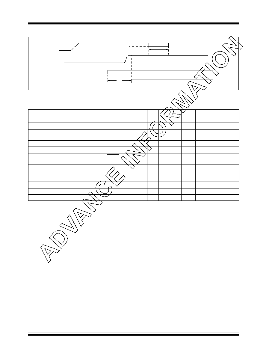
PIC18F2450/4450
DS39760A-page 286
Advance Information
� 2006 Microchip Technology Inc.
FIGURE 21-8:
BROWN-OUT RESET TIMING
TABLE 21-10: RESET, WATCHDOG TIMER, OSCILLATOR START-UP TIMER, POWER-UP TIMER
AND BROWN-OUT RESET REQUIREMENTS
Param.
No.
Symbol
Characteristic
Min
Typ
Max
Units
Conditions
30
TmcL
MCLR Pulse Width (low)
2
--
--
s
31
T
WDT
Watchdog Timer Time-out Period
(no postscaler)
--
4.00
TBD
ms
32
T
OST
Oscillator Start-up Timer Period
1024 T
OSC
--
1024 T
OSC
--
T
OSC
= OSC1 period
33
T
PWRT
Power-up Timer Period
--
65.5
TBD
ms
34
T
IOZ
I/O High-Impedance from MCLR
Low or Watchdog Timer Reset
--
2
--
s
35
T
BOR
Brown-out Reset Pulse Width
200
--
--
s
V
DD
B
VDD
(see D005)
36
T
IRVST
Time for Internal Reference
Voltage to become Stable
--
20
50
s
37
T
LVD
Low-Voltage Detect Pulse Width
200
--
--
s
V
DD
V
LVD
38
T
CSD
CPU Start-up Time
5
--
10
s
39
T
IOBST
Time for INTRC to Stabilize
--
1
--
ms
Legend: TBD = To Be Determined
V
DD
BV
DD
35
V
BGAP
= 1.2V
V
IRVST
Enable Internal
Internal Reference
36
Reference Voltage
Voltage Stable
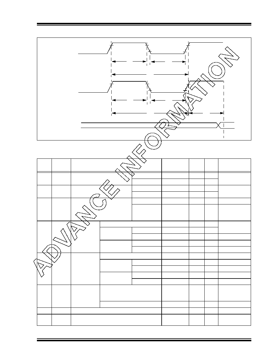
PIC18F2450/4450
� 2006 Microchip Technology Inc.
Advance Information
DS39760A-page 287
FIGURE 21-9:
TIMER0 AND TIMER1 EXTERNAL CLOCK TIMINGS
TABLE 21-11: TIMER0 AND TIMER1 EXTERNAL CLOCK REQUIREMENTS
Note:
Refer to Figure 21-4 for load conditions.
46
47
45
48
41
42
40
T0CKI
T1OSO/T1CKI
TMR0 or
TMR1
Param
No.
Symbol
Characteristic
Min
Max
Units
Conditions
40
Tt0H
T0CKI High Pulse Width
No prescaler
0.5 T
CY
+ 20
--
ns
With prescaler
10
--
ns
41
Tt0L
T0CKI Low Pulse Width
No prescaler
0.5 T
CY
+ 20
--
ns
With prescaler
10
--
ns
42
Tt0P
T0CKI Period
No prescaler
T
CY
+ 10
--
ns
With prescaler
Greater of:
20 ns or
(T
CY
+ 40)/N
--
ns
N = prescale
value
(1, 2, 4,..., 256)
45
Tt1H
T1CKI High
Time
Synchronous, no prescaler
0.5 T
CY
+ 20
--
ns
Synchronous,
with prescaler
PIC18FXXXX
10
--
ns
PIC18LFXXXX
25
--
ns
V
DD
= 2.0V
Asynchronous
PIC18FXXXX
30
--
ns
PIC18LFXXXX
50
--
ns
V
DD
= 2.0V
46
Tt1L
T1CKI Low
Time
Synchronous, no prescaler
0.5 T
CY
+ 5
--
ns
Synchronous,
with prescaler
PIC18FXXXX
10
--
ns
PIC18LFXXXX
25
--
ns
V
DD
= 2.0V
Asynchronous
PIC18FXXXX
30
--
ns
PIC18LFXXXX
50
--
ns
V
DD
= 2.0V
47
Tt1P
T1CKI Input
Period
Synchronous
Greater of:
20 ns or
(T
CY
+ 40)/N
--
ns
N = prescale
value (1, 2, 4, 8)
Asynchronous
60
--
ns
Ft1
T1CKI Oscillator Input Frequency Range
DC
50
kHz
48
Tcke2tmrI Delay from External T1CKI Clock Edge to Timer
Increment
2 T
OSC
7 T
OSC
--
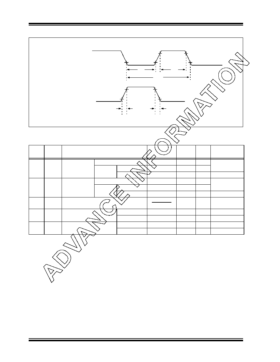
PIC18F2450/4450
DS39760A-page 288
Advance Information
� 2006 Microchip Technology Inc.
FIGURE 21-10:
CAPTURE/COMPARE/PWM TIMINGS (CCP MODULE)
TABLE 21-12: CAPTURE/COMPARE/PWM REQUIREMENTS
Note:
Refer to Figure 21-4 for load conditions.
CCP1
(Capture Mode)
50
51
52
CCP1
53
54
(Compare or PWM Mode)
Param
No.
Symbol
Characteristic
Min
Max
Units
Conditions
50
TccL
CCP1 Input
Low Time
No prescaler
0.5 T
CY
+ 20
--
ns
With
prescaler
PIC18FXXXX
10
--
ns
PIC18LFXXXX
20
--
ns
V
DD
= 2.0V
51
TccH
CCP1 Input
High Time
No prescaler
0.5 T
CY
+ 20
--
ns
With
prescaler
PIC18FXXXX
10
--
ns
PIC18LFXXXX
20
--
ns
V
DD
= 2.0V
52
TccP
CCP1 Input Period
3 T
CY
+ 40
N
--
ns
N = prescale
value (1, 4 or 16)
53
TccR
CCP1 Output Fall Time
PIC18FXXXX
--
25
ns
PIC18LFXXXX
--
45
ns
V
DD
= 2.0V
54
TccF
CCP1 Output Fall Time
PIC18FXXXX
--
25
ns
PIC18LFXXXX
--
45
ns
V
DD
= 2.0V
PIC18F2450/4450
� 2006 Microchip Technology Inc.
Advance Information
DS39760A-page 289
FIGURE 21-11:
EUSART SYNCHRONOUS TRANSMISSION (MASTER/SLAVE) TIMING
TABLE 21-13: EUSART SYNCHRONOUS TRANSMISSION REQUIREMENTS
FIGURE 21-12:
EUSART SYNCHRONOUS RECEIVE (MASTER/SLAVE) TIMING
TABLE 21-14: EUSART SYNCHRONOUS RECEIVE REQUIREMENTS
121
121
120
122
RC6/TX/CK
RC7/RX/DT
pin
pin
Note:
Refer to Figure 21-4 for load conditions.
Param
No.
Symbol
Characteristic
Min
Max
Units
Conditions
120
TckH2dtV SYNC XMIT (MASTER & SLAVE)
Clock High to Data Out Valid
PIC18FXXXX
--
40
ns
PIC18LFXXXX
--
100
ns
V
DD
= 2.0V
121
Tckrf
Clock Out Rise Time and Fall Time
(Master mode)
PIC18FXXXX
--
20
ns
PIC18LFXXXX
--
50
ns
V
DD
= 2.0V
122
Tdtrf
Data Out Rise Time and Fall Time
PIC18FXXXX
--
20
ns
PIC18LFXXXX
--
50
ns
V
DD
= 2.0V
125
126
RC6/TX/CK
RC7/RX/DT
pin
pin
Note:
Refer to Figure 21-4 for load conditions.
Param.
No.
Symbol
Characteristic
Min
Max
Units
Conditions
125
T
DT
V2
CKL
SYNC RCV (MASTER & SLAVE)
Data Hold before CK
(DT hold time)
10
--
ns
126
T
CK
L2
DTL
Data Hold after CK
(DT hold time)
15
--
ns
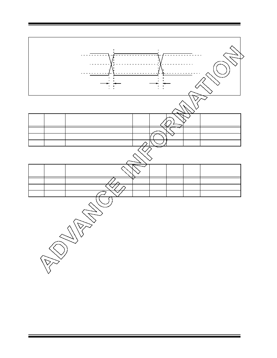
PIC18F2450/4450
DS39760A-page 290
Advance Information
� 2006 Microchip Technology Inc.
FIGURE 21-13:
USB SIGNAL TIMING
TABLE 21-15: USB LOW-SPEED TIMING REQUIREMENTS
TABLE 21-16: USB FULL-SPEED REQUIREMENTS
V
CRS
USB Data Differential Lines
90%
10%
T
LR
, T
FR
T
LF
, T
FF
Param
No.
Symbol
Characteristic
Min
Typ
Max
Units
Conditions
T
LR
Transition Rise Time
75
--
300
ns
C
L
= 200 to 600 pF
T
LF
Transition Fall Time
75
--
300
ns
C
L
= 200 to 600 pF
T
LRFM
Rise/Fall Time Matching
80
--
125
%
Param
No.
Symbol
Characteristic
Min
Typ
Max
Units
Conditions
T
FR
Transition Rise Time
4
--
20
ns
C
L
= 50 pF
T
FF
Transition Fall Time
4
--
20
ns
C
L
= 50 pF
T
FRFM
Rise/Fall Time Matching
90
--
111.1
%
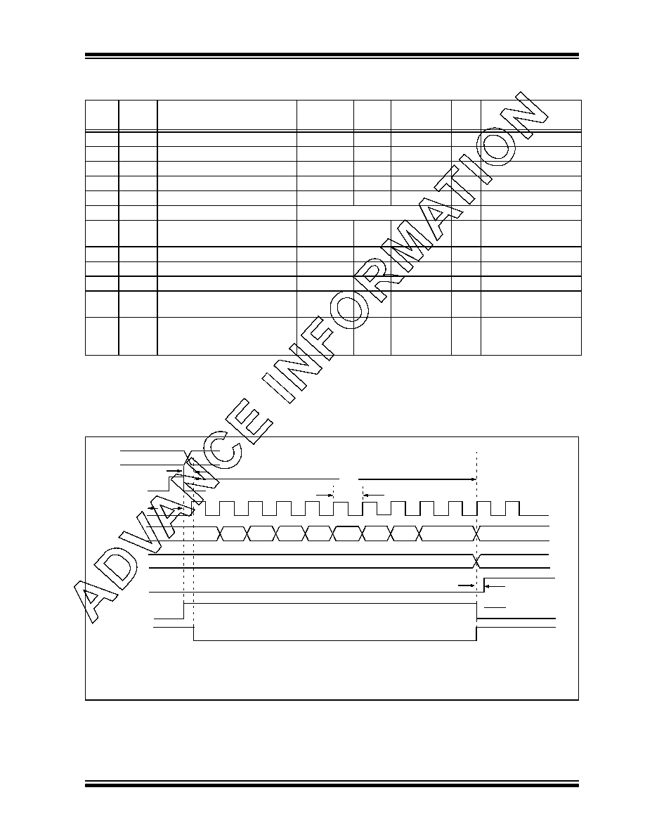
PIC18F2450/4450
� 2006 Microchip Technology Inc.
Advance Information
DS39760A-page 291
TABLE 21-17: A/D CONVERTER CHARACTERISTICS: PIC18F2450/4450 (INDUSTRIAL)
PIC18LF2450/4450 (INDUSTRIAL)
FIGURE 21-14:
A/D CONVERSION TIMING
Param
No.
Symbol
Characteristic
Min
Typ
Max
Units
Conditions
A01
N
R
Resolution
--
--
10
bit
V
REF
3.0V
A03
E
IL
Integral Linearity Error
--
--
<�1
LSb
V
REF
3.0V
A04
E
DL
Differential Linearity Error
--
--
<�1
LSb
V
REF
3.0V
A06
E
OFF
Offset Error
--
--
<�1.5
LSb
V
REF
3.0V
A07
E
GN
Gain Error
--
--
<�1
LSb
V
REF
3.0V
A10
--
Monotonicity
Guaranteed
(1)
--
V
SS
V
AIN
V
REF
A20
V
REF
Reference Voltage Range
(V
REFH
� V
REFL
)
1.8
3
--
--
--
--
V
V
V
DD
< 3.0V
V
DD
3.0V
A21
V
REFH
Reference Voltage High
V
SS
--
V
REFH
V
A22
V
REFL
Reference Voltage Low
V
SS
� 0.3V
--
V
DD
� 3.0V
V
A25
V
AIN
Analog Input Voltage
V
REFL
--
V
REFH
V
A30
Z
AIN
Recommended Impedance of
Analog Voltage Source
--
--
2.5
k
A50
I
REF
V
REF
Input Current
(2)
--
--
--
--
5
150
A
A
During V
AIN
acquisition.
During A/D conversion
cycle.
Note 1:
The A/D conversion result never decreases with an increase in the input voltage and has no missing codes.
2:
V
REFH
current is from RA3/AN3/V
REF
+ pin or V
DD
, whichever is selected as the V
REFH
source.
V
REFL
current is from RA2/AN2/V
REF
- pin or V
SS
, whichever is selected as the V
REFL
source.
131
130
132
BSF ADCON0, GO
Q4
A/D CLK
A/D DATA
ADRES
ADIF
GO
SAMPLE
OLD_DATA
SAMPLING STOPPED
DONE
NEW_DATA
(Note 2)
9
8
7
2
1
0
Note
1:
If the A/D clock source is selected as RC, a time of T
CY
is added before the A/D clock starts. This allows the SLEEP instruction
to be executed.
2:
This is a minimal RC delay (typically 100 ns), which also disconnects the holding capacitor from the analog input.
. . .
. . .
T
CY
(1)

PIC18F2450/4450
DS39760A-page 292
Advance Information
� 2006 Microchip Technology Inc.
TABLE 21-18: A/D CONVERSION REQUIREMENTS
Param
No.
Symbol
Characteristic
Min
Max
Units
Conditions
130
T
AD
A/D Clock Period
PIC18FXXXX
0.7
25.0
(1)
s
T
OSC
based, V
REF
3.0V
PIC18LFXXXX
1.4
25.0
(1)
s
V
DD
= 2.0V,
T
OSC
based, V
REF
full range
PIC18FXXXX
TBD
1
s
A/D RC mode
PIC18LFXXXX
TBD
3
s
V
DD
= 2.0V,
A/D RC mode
131
T
CNV
Conversion Time
(not including acquisition time)
(2)
11
12
T
AD
132
T
ACQ
Acquisition Time
(3)
1.4
TBD
--
--
s
s
-40
�C to +85�C
0
�C to +85�C
135
T
SWC
Switching Time from Convert
Sample
--
(Note 4)
137
T
DIS
Discharge Time
0.2
--
s
Legend: TBD = To Be Determined
Note 1:
The time of the A/D clock period is dependent on the device frequency and the T
AD
clock divider.
2:
ADRES registers may be read on the following T
CY
cycle.
3:
The time for the holding capacitor to acquire the "New" input voltage when the voltage changes full scale
after the conversion (V
DD
to V
SS
or V
SS
to V
DD
). The source impedance (
R
S
) on the input channels is 50
.
4:
On the following cycle of the device clock.

PIC18F2450/4450
� 2006 Microchip Technology Inc.
Advance Information
DS39760A-page 293
22.0
DC AND AC
CHARACTERISTICS GRAPHS
AND TABLES
Graphs and tables are not available at this time.

PIC18F2450/4450
DS39760A-page 294
Advance Information
� 2006 Microchip Technology Inc.
NOTES:
PIC18F2450/4450
� 2006 Microchip Technology Inc.
Advance Information
DS39760A-page 295
23.0
PACKAGING INFORMATION
23.1
Package Marking Information
28-Lead PDIP (Skinny DIP)
XXXXXXXXXXXXXXXXX
XXXXXXXXXXXXXXXXX
YYWWNNN
Example
PIC18F2450-I/SP
0510017
28-Lead SOIC
XXXXXXXXXXXXXXXXXXXX
XXXXXXXXXXXXXXXXXXXX
XXXXXXXXXXXXXXXXXXXX
YYWWNNN
Example
PIC18F2450-E/SO
0510017
28-Lead QFN
XXXXXXXX
XXXXXXXX
YYWWNNN
Example
18F2450
-I/ML
0510017
3
e
3
e
3
e
Legend: XX...X
Customer-specific information
Y
Year code (last digit of calendar year)
YY
Year code (last 2 digits of calendar year)
WW
Week code (week of January 1 is week `01')
NNN
Alphanumeric traceability code
Pb-free JEDEC designator for Matte Tin (Sn)
*
This package is Pb-free. The Pb-free JEDEC designator ( )
can be found on the outer packaging for this package.
Note:
In the event the full Microchip part number cannot be marked on one line, it will
be carried over to the next line, thus limiting the number of available
characters for customer-specific information.
3
e
3
e
PIC18F2450/4450
DS39760A-page 296
Advance Information
� 2006 Microchip Technology Inc.
Package Marking Information (Continued)
44-Lead TQFP
XXXXXXXXXX
XXXXXXXXXX
XXXXXXXXXX
YYWWNNN
Example
PIC18F4450
-I/PT
0510017
XXXXXXXXXX
44-Lead QFN
XXXXXXXXXX
XXXXXXXXXX
YYWWNNN
PIC18F4450
Example
-I/ML
0510017
40-Lead PDIP
XXXXXXXXXXXXXXXXXX
XXXXXXXXXXXXXXXXXX
XXXXXXXXXXXXXXXXXX
YYWWNNN
Example
PIC18F4450-I/P
0510017
3
e
3
e
3
e
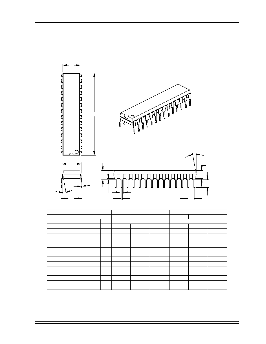
PIC18F2450/4450
� 2006 Microchip Technology Inc.
Advance Information
DS39760A-page 297
23.2
Package Details
The following sections give the technical details of the
packages.
28-Lead Skinny Plastic Dual In-line (SP) � 300 mil Body (PDIP)
15
10
5
15
10
5
Mold Draft Angle Bottom
15
10
5
15
10
5
Mold Draft Angle Top
10.92
8.89
8.13
.430
.350
.320
eB
Overall Row Spacing
�
0.56
0.48
0.41
.022
.019
.016
B
Lower Lead Width
1.65
1.33
1.02
.065
.053
.040
B1
Upper Lead Width
0.38
0.29
0.20
.015
.012
.008
c
Lead Thickness
3.43
3.30
3.18
.135
.130
.125
L
Tip to Seating Plane
35.18
34.67
34.16
1.385
1.365
1.345
D
Overall Length
7.49
7.24
6.99
.295
.285
.275
E1
Molded Package Width
8.26
7.87
7.62
.325
.310
.300
E
Shoulder to Shoulder Width
0.38
.015
A1
Base to Seating Plane
3.43
3.30
3.18
.135
.130
.125
A2
Molded Package Thickness
4.06
3.81
3.56
.160
.150
.140
A
Top to Seating Plane
2.54
.100
p
Pitch
28
28
n
Number of Pins
MAX
NOM
MIN
MAX
NOM
MIN
Dimension Limits
MILLIMETERS
INCHES*
Units
2
1
D
n
E1
c
eB
E
p
L
A2
B
B1
A
A1
Notes:
JEDEC Equivalent: MO-095
Drawing No. C04-070
* Controlling Parameter
Dimension D and E1 do not include mold flash or protrusions. Mold flash or protrusions shall not exceed .010" (0.254mm) per side.
� Significant Characteristic
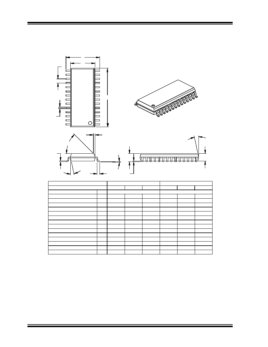
PIC18F2450/4450
DS39760A-page 298
Advance Information
� 2006 Microchip Technology Inc.
28-Lead Plastic Small Outline (SO) � Wide, 300 mil Body (SOIC)
Foot Angle Top
0
4
8
0
4
8
15
12
0
15
12
0
Mold Draft Angle Bottom
15
12
0
15
12
0
Mold Draft Angle Top
0.51
0.42
0.36
.020
.017
.014
B
Lead Width
0.33
0.28
0.23
.013
.011
.009
c
Lead Thickness
1.27
0.84
0.41
.050
.033
.016
L
Foot Length
0.74
0.50
0.25
.029
.020
.010
h
Chamfer Distance
18.08
17.87
17.65
.712
.704
.695
D
Overall Length
7.59
7.49
7.32
.299
.295
.288
E1
Molded Package Width
10.67
10.34
10.01
.420
.407
.394
E
Overall Width
0.30
0.20
0.10
.012
.008
.004
A1
Standoff
�
2.39
2.31
2.24
.094
.091
.088
A2
Molded Package Thickness
2.64
2.50
2.36
.104
.099
.093
A
Overall Height
1.27
.050
p
Pitch
28
28
n
Number of Pins
MAX
NOM
MIN
MAX
NOM
MIN
Dimension Limits
MILLIMETERS
INCHES*
Units
2
1
D
p
n
B
E
E1
L
c
45
�
h
A2
A
A1
* Controlling Parameter
Notes:
Dimensions D and E1 do not include mold flash or protrusions. Mold flash or protrusions shall not exceed .010" (0.254mm) per side.
JEDEC Equivalent: MS-013
Drawing No. C04-052
� Significant Characteristic
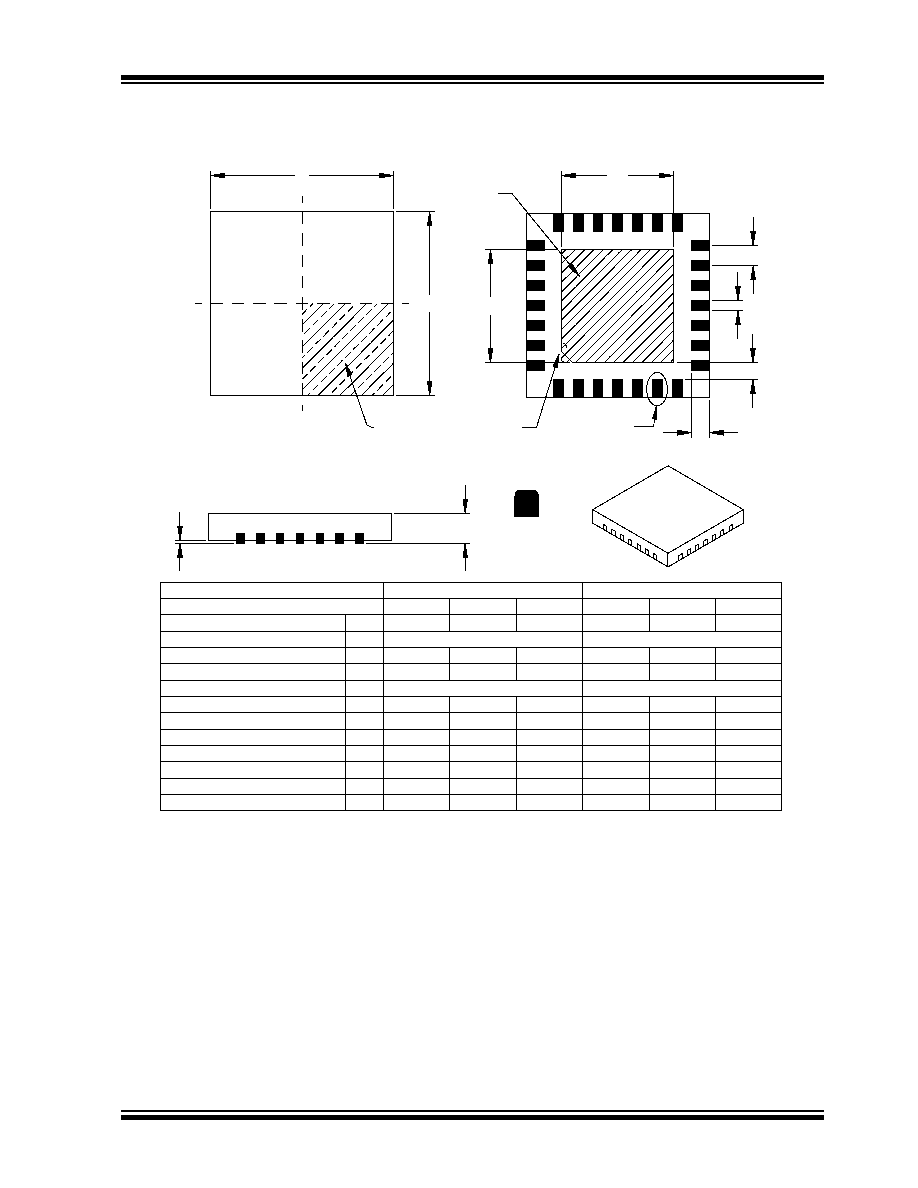
PIC18F2450/4450
� 2006 Microchip Technology Inc.
Advance Information
DS39760A-page 299
28-Lead Plastic Quad Flat No Lead Package (ML) 6x6 mm Body (QFN) �
With 0.55 mm Contact Length (Saw Singulated)
b
D2
D
PAD OUTLINE
ALTERNATE
SEE DETAIL
A1
A
DETAIL
TOP VIEW
OPTIONAL
INDEX
AREA
1
2
L
BOTTOM VIEW
n
E
METAL
PAD
ALTERNATE
EXPOSED
INDICATORS
INDEX
e
E2
(NOTE 1)
(NOTE 2)
K
Contact Width
� Significant Characteristic
Notes:
JEDEC equivalent: MO-220
.009
.011
.013
0.23
0.28
0.33
Pitch
Number of Pins
Overall Width
Standoff
Overall Length
Overall Height
MAX
Units
Dimension Limits
A1
D
E
n
e
A
.000
INCHES
.026 BSC
MIN
28
NOM
MAX
.002
0.00
6.00
MILLIMETERS*
.039
MIN
28
0.65 BSC
NOM
0.05
1.00
0.90
.035
.001
0.02
Contact Length �
L
.018
.022
.024
0.45
0.55
0.65
E2
D2
Exposed Pad Width
Exposed Pad Length
.153
.167
.169
3.89
4.24
4.29
.031
0.80
5.90
6.10
.240
.236
.232
.232
.236
6.00
.240
5.90
6.10
.153
.167
4.24
.169
3.89
4.29
Contact Thickness
A3
.008 REF
0.20 REF
REF: Reference Dimension, usually without tolerance, for information purposes only.
BSC: Basic Dimension. Theoretically exact value shown without tolerances.
See ASME Y14.5M
See ASME Y14.5M
1. Pin 1 visual index feature may vary, but must be located within the hatched area.
2. Exposed pad varies according to die attach paddle size.
Contact-to-Exposed Pad
�
K
.008
�
�
0.20
�
�
* Controlling Parameter
Revised 09-12-05
Drawing No. C04-105
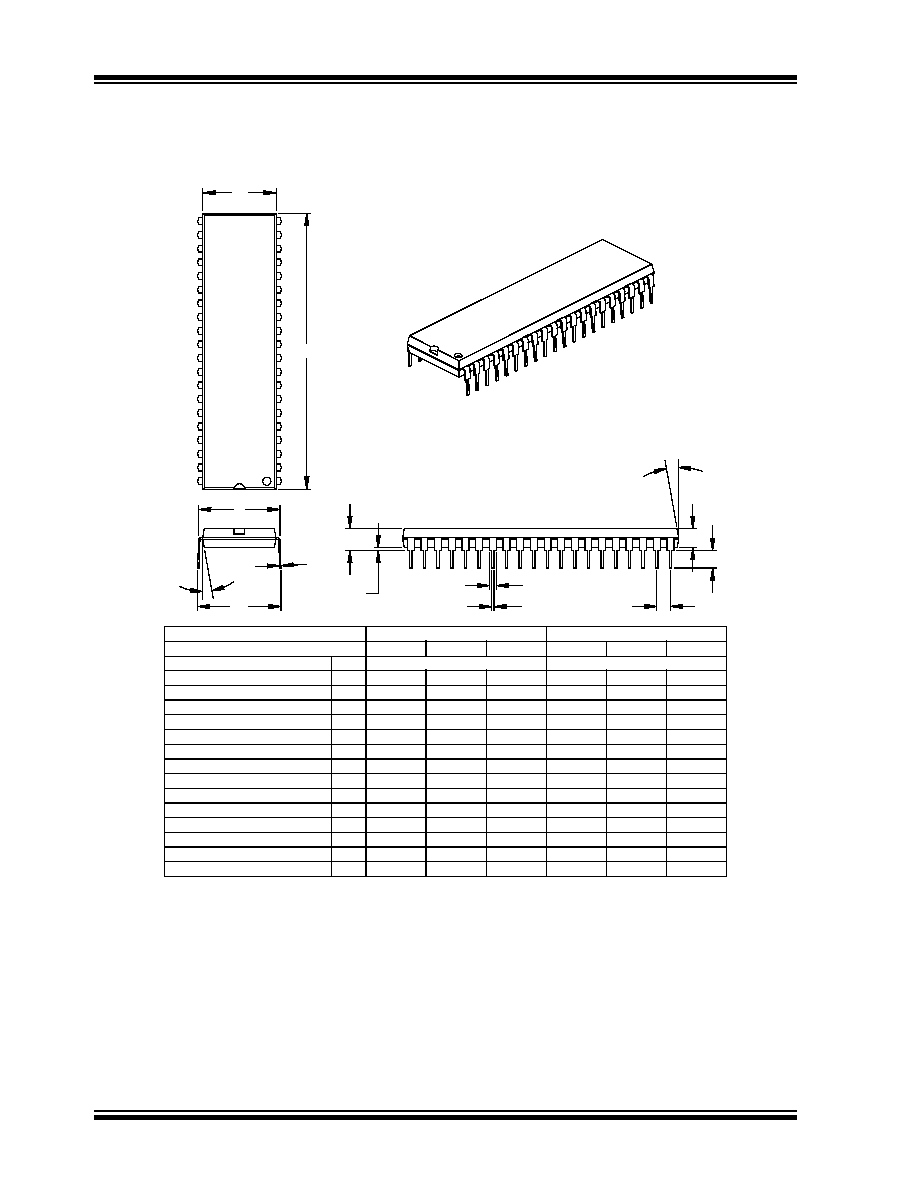
PIC18F2450/4450
DS39760A-page 300
Advance Information
� 2006 Microchip Technology Inc.
40-Lead Plastic Dual In-line (P) � 600 mil Body (PDIP)
15
10
5
15
10
5
Mold Draft Angle Bottom
15
10
5
15
10
5
Mold Draft Angle Top
17.27
16.51
15.75
.680
.650
.620
eB
Overall Row Spacing
�
0.56
0.46
0.36
.022
.018
.014
B
Lower Lead Width
1.78
1.27
0.76
.070
.050
.030
B1
Upper Lead Width
0.38
0.29
0.20
.015
.012
.008
c
Lead Thickness
3.43
3.30
3.05
.135
.130
.120
L
Tip to Seating Plane
52.45
52.26
51.94
2.065
2.058
2.045
D
Overall Length
14.22
13.84
13.46
.560
.545
.530
E1
Molded Package Width
15.88
15.24
15.11
.625
.600
.595
E
Shoulder to Shoulder Width
0.38
.015
A1
Base to Seating Plane
4.06
3.81
3.56
.160
.150
.140
A2
Molded Package Thickness
4.83
4.45
4.06
.190
.175
.160
A
Top to Seating Plane
2.54
.100
p
Pitch
40
40
n
Number of Pins
MAX
NOM
MIN
MAX
NOM
MIN
Dimension Limits
MILLIMETERS
INCHES*
Units
A2
1
2
D
n
E1
c
eB
E
p
L
B
B1
A
A1
* Controlling Parameter
Notes:
Dimensions D and E1 do not include mold flash or protrusions. Mold flash or protrusions shall not exceed .010" (0.254mm) per side.
JEDEC Equivalent: MO-011
Drawing No. C04-016
� Significant Characteristic
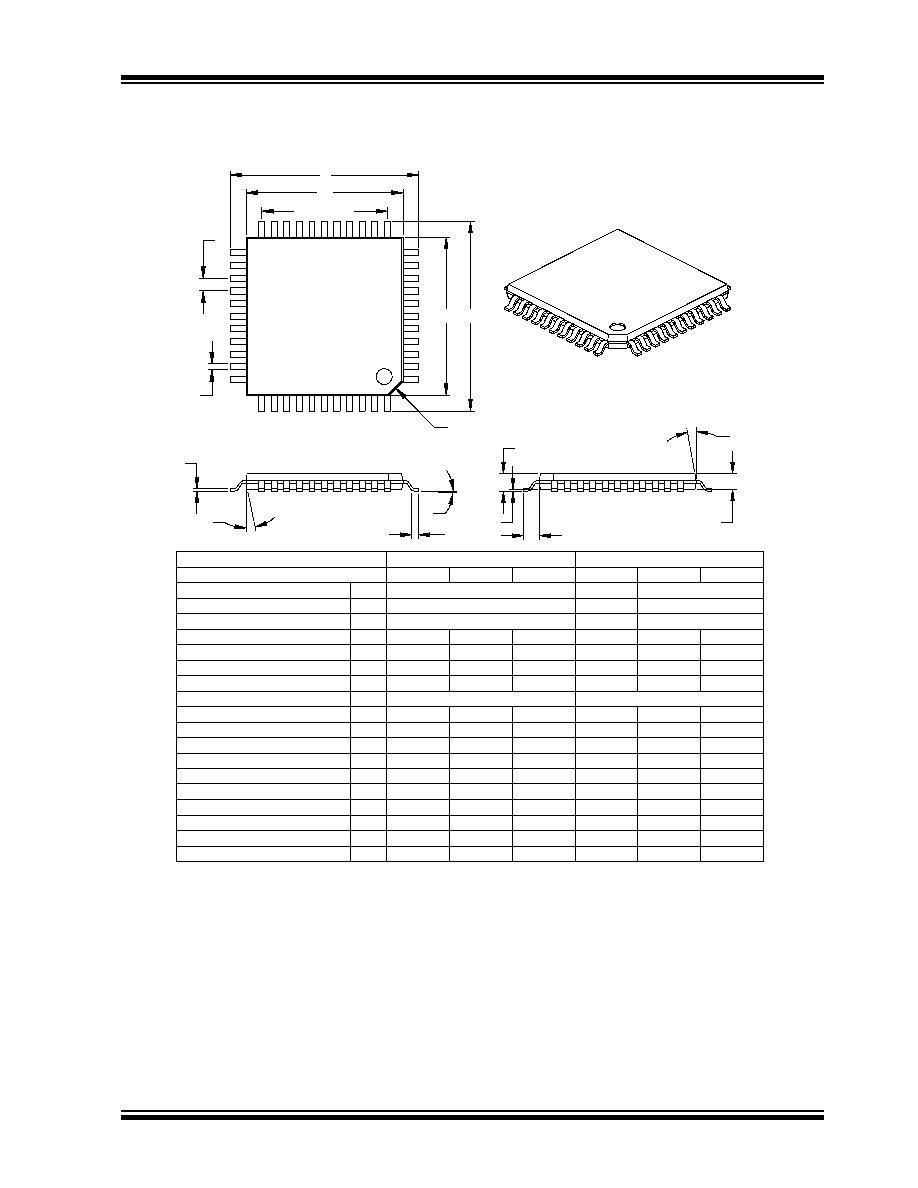
PIC18F2450/4450
� 2006 Microchip Technology Inc.
Advance Information
DS39760A-page 301
44-Lead Plastic Thin-Quad Flatpack (PT) 10x10x1 mm Body, 1.0/0.10 mm Lead Form (TQFP)
F
A
A1
A2
E
E1
#leads=n1
p
B
D1
D
n
1
2
c
L
CH x 45�
1.14
0.89
0.64
.045
.035
.025
CH
Pin 1 Corner Chamfer
1.00 REF.
.039 REF.
F
Footprint (Reference)
Units
INCHES
MILLIMETERS*
Dimension Limits
MIN
NOM
MAX
MIN
NOM
MAX
Number of Pins
n
44
44
Pitch
p
.031
0.80
Overall Height
A
.039
.043
.047
1.00
1.10
1.20
Molded Package Thickness
A2
.037
.039
.041
0.95
1.00
1.05
Standoff
A1
.002
.004
.006
0.05
0.10
0.15
Foot Length
L
.018
.024
.030
0.45
0.60
0.75
Foot Angle
0
3.5
7
0
3.5
7
Overall Width
E
.463
.472
.482
11.75
12.00
12.25
Overall Length
D
.463
.472
.482
11.75
12.00
12.25
Molded Package Width
E1
.390
.394
.398
9.90
10.00
10.10
Molded Package Length
D1
.390
.394
.398
9.90
10.00
10.10
Pins per Side
n1
11
11
Lead Thickness
c
.004
.006
.008
0.09
0.15
0.20
Lead Width
B
.012
.015
.017
0.30
0.38
0.44
Mold Draft Angle Top
5
10
15
5
10
15
Mold Draft Angle Bottom
5
10
15
5
10
15
Dimensions D and E1 do not include mold flash or protrusions. Mold flash or protrusions shall not exceed .010" (0.254mm) per side.
Notes:
JEDEC Equivalent: MS-026
Revised 07-22-05
* Controlling Parameter
REF: Reference Dimension, usually without tolerance, for information purposes only.
See ASME Y14.5M
Drawing No. C04-076
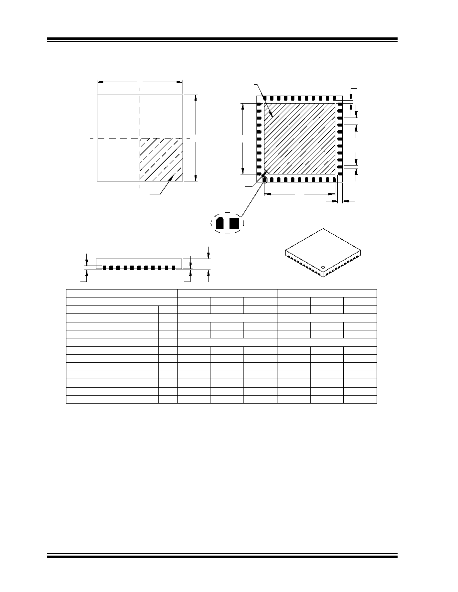
PIC18F2450/4450
DS39760A-page 302
Advance Information
� 2006 Microchip Technology Inc.
44-Lead Plastic Quad Flat No Lead Package (ML) 8x8 mm Body (QFN)
D2
D
TOP VIEW
n
1
L
E2
BOTTOM VIEW
B
E
2
PIN 1
INDEX ON
EXPOSED PAD
(NOTE 1)
INDEX AREA
OPTIONAL
DETAIL: CONTACT VARIANTS
(PROFILE MAY VARY)
p
A1
A
A3
EXPOSED
METAL PAD
(NOTE 2)
K
INCHES
NOM
.026 BSC
.010 REF
BSC: Basic Dimension. Theoretically exact value shown without tolerances.
REF: Reference Dimension, usually without tolerance, for information purposes only.
Number of Contacts
Overall Height
See ASME Y14.5M
See ASME Y14.5M
Contact Width
* Controlling Parameter
Overall Width
Overall Length
Contact Length
�
Exposed Pad Width
Exposed Pad Length
JEDEC equivalent: M0-220
Base Thickness
Notes:
Pitch
Standoff
Units
Dimension Limits
A1
A
B
D
E2
D2
A3
p
.000
.309
.309
.236
.236
.014
.008
L
E
.031
MIN
n
.258
.013
.016
.315
.258
.315
.035
.001
.260
.321
.013
.019
.260
.002
.039
.321
MAX
44
0.65 BSC
0.25 REF
7.85
5.99
5.99
0.35
0.20
0.80
7.85
0
0.33
8.00
0.40
6.55
6.55
0.90
0.02
8.00
MILLIMETERS*
MIN
NOM
44
8.15
6.60
6.60
0.48
0.35
1.00
0.05
8.15
MAX
1. Pin 1 visual index feature may vary, but must be located within the hatched area.
2. Exposed pad varies according to die attach paddle size.
Contact-to-Exposed-Pad
�
K
.014
-
-
0.20
-
-
� Significant Characteristic
Revised 09-12-05
Drawing No. C04-103

PIC18F2450/4450
� 2006 Microchip Technology Inc.
Advance Information
DS39760A-page 303
APPENDIX A:
REVISION HISTORY
Revision A (January 2006)
Original data sheet for PIC18F2450/4450 devices.
APPENDIX B:
DEVICE
DIFFERENCES
The differences between the devices listed in this data
sheet are shown in Table B-1.
TABLE B-1:
DEVICE DIFFERENCES
Features
PIC18F2450
PIC18F4450
Program Memory (Bytes)
16384
16384
Program Memory (Instructions)
8192
8192
Interrupt Sources
13
13
I/O Ports
Ports A, B, C, (E)
Ports A, B, C, D, E
Capture/Compare/PWM Modules
1
1
10-bit Analog-to-Digital Module
10 input channels
13 input channels
Packages
28-pin SDIP
28-pin SOIC
28-pin QFN
40-pin PDIP
44-pin TQFP
44-pin QFN

PIC18F2450/4450
DS39760A-page 304
Advance Information
� 2006 Microchip Technology Inc.
APPENDIX C:
CONVERSION
CONSIDERATIONS
This appendix discusses the considerations for
converting from previous versions of a device to the
ones listed in this data sheet. Typically, these changes
are due to the differences in the process technology
used. An example of this type of conversion is from a
PIC16C74A to a PIC16C74B.
Not Applicable
APPENDIX D:
MIGRATION FROM
BASELINE TO
ENHANCED DEVICES
This section discusses how to migrate from a Baseline
device (i.e., PIC16C5X) to an Enhanced MCU device
(i.e., PIC18FXXX).
The following are the list of modifications over the
PIC16C5X microcontroller family:
Not Currently Available

PIC18F2450/4450
� 2006 Microchip Technology Inc.
Advance Information
DS39760A-page 305
APPENDIX E:
MIGRATION FROM
MID-RANGE TO
ENHANCED DEVICES
A detailed discussion of the differences between the
mid-range MCU devices (i.e., PIC16CXXX) and the
enhanced devices (i.e., PIC18FXXX) is provided in
AN716, "Migrating Designs from PIC16C74A/74B to
PIC18C442". The changes discussed, while device
specific, are generally applicable to all mid-range to
enhanced device migrations.
This Application Note is available as Literature Number
DS00716.
APPENDIX F:
MIGRATION FROM
HIGH-END TO
ENHANCED DEVICES
A detailed discussion of the migration pathway and
differences between the high-end MCU devices (i.e.,
PIC17CXXX) and the enhanced devices (i.e.,
PIC18FXXX) is provided in
AN726, "PIC17CXXX to
PIC18CXXX Migration". This Application Note is
available as Literature Number DS00726.

PIC18F2450/4450
DS39760A-page 306
Advance Information
� 2006 Microchip Technology Inc.
NOTES:

PIC18F2450/4450
� 2006 Microchip Technology Inc.
Advance Information
DS39760A-page 307
INDEX
A
A/D ................................................................................... 173
Acquisition Requirements ........................................ 178
ADCON0 Register .................................................... 173
ADCON1 Register .................................................... 173
ADCON2 Register .................................................... 173
ADRESH Register ............................................ 173, 176
ADRESL Register .................................................... 173
Analog Port Pins, Configuring .................................. 180
Associated Registers ............................................... 182
Configuring the Module ............................................ 177
Conversion Clock (T
AD
) ........................................... 179
Conversion Requirements ....................................... 292
Conversion Status (GO/DONE Bit) .......................... 176
Conversions ............................................................. 181
Converter Characteristics ........................................ 291
Converter Interrupt, Configuring .............................. 177
Discharge ................................................................. 181
Operation in Power-Managed Modes ...................... 180
Selecting and Configuring Acquisition Time ............ 179
Special Event Trigger (CCP1) .................................. 182
Use of the CCP1 Trigger .......................................... 182
Absolute Maximum Ratings ............................................. 265
AC (Timing) Characteristics ............................................. 281
Load Conditions for Device
Timing Specifications ....................................... 282
Parameter Symbology ............................................. 281
Temperature and Voltage Specifications ................. 282
Timing Conditions .................................................... 282
AC Characteristics
Internal RC Accuracy ............................................... 284
ADCON0 Register ............................................................ 173
GO/DONE Bit ........................................................... 176
ADCON1 Register ............................................................ 173
ADCON2 Register ............................................................ 173
ADDFSR .......................................................................... 254
ADDLW ............................................................................ 217
ADDULNK ........................................................................ 254
ADDWF ............................................................................ 217
ADDWFC ......................................................................... 218
ADRESH Register ............................................................ 173
ADRESL Register .................................................... 173, 176
Analog-to-Digital Converter.
See
A/D.
ANDLW ............................................................................ 218
ANDWF ............................................................................ 219
Assembler
MPASM Assembler .................................................. 262
Auto-Wake-up on Sync Break Character ......................... 166
B
BC .................................................................................... 219
BCF .................................................................................. 220
Block Diagrams
A/D ........................................................................... 176
Analog Input Model .................................................. 177
Capture Mode Operation ......................................... 124
Compare Mode Operation ....................................... 125
Device Clock .............................................................. 24
EUSART Receive .................................................... 164
EUSART Transmit ................................................... 162
External Power-on Reset Circuit
(Slow V
DD
Power-up) ......................................... 43
Fail-Safe Clock Monitor ........................................... 204
Generic I/O Port ......................................................... 99
High/Low-Voltage Detect with External Input .......... 184
Interrupt Logic ............................................................ 86
On-Chip Reset Circuit ................................................ 41
PIC18F2450 .............................................................. 10
PIC18F4450 .............................................................. 11
PLL (HS Mode) .......................................................... 26
PWM Operation (Simplified) .................................... 127
Reads from Flash Program Memory ......................... 77
Table Read Operation ............................................... 73
Table Write Operation ............................................... 74
Table Writes to Flash Program Memory .................... 79
Timer0 in 16-Bit Mode ............................................. 112
Timer0 in 8-Bit Mode ............................................... 112
Timer1 ..................................................................... 116
Timer1 (16-Bit Read/Write Mode) ............................ 116
Timer2 ..................................................................... 122
USB Interrupt Logic Funnel ..................................... 143
USB Peripheral and Options ................................... 129
Watchdog Timer ...................................................... 201
BN .................................................................................... 220
BNC ................................................................................. 221
BNN ................................................................................. 221
BNOV .............................................................................. 222
BNZ ................................................................................. 222
BOR.
See
Brown-out Reset.
BOV ................................................................................. 225
BRA ................................................................................. 223
Brown-out Reset (BOR) ..................................................... 44
Detecting ................................................................... 44
Disabling in Sleep Mode ............................................ 44
Software Enabled ...................................................... 44
BSF .................................................................................. 223
BTFSC ............................................................................. 224
BTFSS ............................................................................. 224
BTG ................................................................................. 225
BZ .................................................................................... 226
C
C Compilers
MPLAB C18 ............................................................. 262
MPLAB C30 ............................................................. 262
CALL ................................................................................ 226
CALLW ............................................................................ 255
Capture (CCP Module) .................................................... 124
Associated Registers ............................................... 126
CCP1 Pin Configuration .......................................... 124
CCPR1H:CCPR1L Registers .................................. 124
Prescaler ................................................................. 124
Software Interrupt .................................................... 124
Capture/Compare/PWM (CCP) ....................................... 123
Capture Mode.
See
Capture.
CCP Mode and Timer Resources ............................ 124
CCPR1H Register ................................................... 124
CCPR1L Register .................................................... 124
Compare Mode.
See
Compare.
Module Configuration .............................................. 124
Clock Sources .................................................................... 30
Selection Using OSCCON Register .......................... 30
CLRF ............................................................................... 227
CLRWDT ......................................................................... 227

PIC18F2450/4450
DS39760A-page 308
Advance Information
� 2006 Microchip Technology Inc.
Code Examples
16 x 16 Signed Multiply Routine ................................ 84
16 x 16 Unsigned Multiply Routine ............................ 84
8 x 8 Signed Multiply Routine .................................... 83
8 x 8 Unsigned Multiply Routine ................................ 83
Changing Between Capture Prescalers ................... 124
Computed GOTO Using an Offset Value ................... 56
Erasing a Flash Program Memory Row ..................... 78
Fast Register Stack .................................................... 56
How to Clear RAM (Bank 1) Using
Indirect Addressing ............................................ 67
Implementing a Real-Time Clock Using
a Timer1 Interrupt Service ............................... 119
Initializing PORTA ...................................................... 99
Initializing PORTB .................................................... 101
Initializing PORTC .................................................... 104
Initializing PORTD .................................................... 107
Initializing PORTE .................................................... 109
Reading a Flash Program Memory Word .................. 77
Saving STATUS, WREG and
BSR Registers in RAM ....................................... 97
Writing to Flash Program Memory ....................... 80�81
Code Protection ............................................................... 189
COMF ............................................................................... 228
Compare (CCP Module) ................................................... 125
Associated Registers ............................................... 126
CCP1 Pin Configuration ........................................... 125
CCPR1 Register ...................................................... 125
Software Interrupt .................................................... 125
Special Event Trigger ............................................... 125
Timer1 Mode Selection ............................................ 125
Configuration Bits ............................................................. 190
Configuration Register Protection .................................... 209
Context Saving During Interrupts ....................................... 97
Conversion Considerations .............................................. 304
CPFSEQ .......................................................................... 228
CPFSGT ........................................................................... 229
CPFSLT ........................................................................... 229
Crystal Oscillator/Ceramic Resonator ................................ 25
Customer Change Notification Service ............................ 315
Customer Notification Service .......................................... 315
Customer Support ............................................................ 315
D
Data Addressing Modes ..................................................... 67
Comparing Addressing Modes with
the Extended Instruction Set Enabled ................ 71
Direct .......................................................................... 67
Indexed Literal Offset ................................................. 70
BSR Operation ................................................... 72
Instructions Affected .......................................... 70
Mapping the Access Bank ................................. 72
Indirect ....................................................................... 67
Inherent and Literal .................................................... 67
Data Memory ...................................................................... 59
Access Bank .............................................................. 61
and the Extended Instruction Set ............................... 70
Bank Select Register (BSR) ....................................... 59
General Purpose Registers ........................................ 61
Map for PIC18F2450/4450 Devices ........................... 60
Special Function Registers ........................................ 62
Map .................................................................... 62
USB RAM ................................................................... 59
DAW ................................................................................. 230
DC and AC Characteristics
Graphs and Tables .................................................. 293
DC Characteristics ........................................................... 276
Power-Down and Supply Current ............................ 268
Supply Voltage ........................................................ 267
DCFSNZ .......................................................................... 231
DECF ............................................................................... 230
DECFSZ .......................................................................... 231
Dedicated ICD/ICSP Port ................................................ 209
Development Support ...................................................... 261
Device Differences ........................................................... 303
Device Overview .................................................................. 7
Features (table) ........................................................... 9
New Core Features ...................................................... 7
Other Special Features ................................................ 8
Direct Addressing .............................................................. 68
E
Effect on Standard PIC MCU Instructions ....................... 258
Electrical Characteristics ................................................. 265
Enhanced Universal Synchronous Receiver
Transmitter (USART).
See
EUSART.
Equations
A/D Acquisition Time ............................................... 178
A/D Minimum Charging Time ................................... 178
Calculating the Minimum Required
A/D Acquisition Time ....................................... 178
Errata ................................................................................... 6
EUSART
Asynchronous Mode ................................................ 162
Associated Registers, Receive ........................ 165
Associated Registers, Transmit ....................... 163
Auto-Wake-up on Sync Break ......................... 166
Break Character Sequence ............................. 167
Receiver .......................................................... 164
Setting Up 9-Bit Mode with Address Detect .... 164
Transmitter ...................................................... 162
Baud Rate Generator (BRG) ................................... 157
Associated Registers ....................................... 157
Auto-Baud Rate Detect .................................... 160
Baud Rate Error, Calculating ........................... 157
Baud Rates, Asynchronous Modes ................. 158
High Baud Rate Select (BRGH Bit) ................. 157
Operation in Power-Managed Modes .............. 157
Sampling .......................................................... 157
Synchronous Master Mode ...................................... 168
Associated Registers, Receive ........................ 170
Associated Registers, Transmit ....................... 169
Reception ........................................................ 170
Transmission ................................................... 168
Synchronous Slave Mode ........................................ 171
Associated Registers, Receive ........................ 172
Associated Registers, Transmit ....................... 171
Reception ........................................................ 172
Transmission ................................................... 171
Extended Instruction Set .................................................. 253
ADDFSR .................................................................. 254
ADDULNK ................................................................ 254
and Using MPLAB IDE Tools ................................... 260
CALLW .................................................................... 255
Considerations for Use ............................................ 258
MOVSF .................................................................... 255
MOVSS .................................................................... 256
PUSHL ..................................................................... 256
SUBFSR .................................................................. 257
SUBULNK ................................................................ 257
Syntax ...................................................................... 253
External Clock Input ........................................................... 26

PIC18F2450/4450
� 2006 Microchip Technology Inc.
Advance Information
DS39760A-page 309
F
Fail-Safe Clock Monitor ............................................ 189, 204
Interrupts in Power-Managed Modes ....................... 205
POR or Wake-up from Sleep ................................... 205
WDT During Oscillator Failure ................................. 204
Fast Register Stack ............................................................ 56
Firmware Instructions ....................................................... 211
Flash Program Memory ..................................................... 73
Associated Registers ................................................. 81
Control Registers ....................................................... 74
EECON1 and EECON2 ..................................... 74
TABLAT (Table Latch) Register ......................... 76
TBLPTR (Table Pointer) Register ...................... 76
Erase Sequence ........................................................ 78
Erasing ....................................................................... 78
Operation During Code-Protect ................................. 81
Protection Against Spurious Writes ........................... 81
Reading ...................................................................... 77
Table Pointer
Boundaries Based on Operation ........................ 76
Table Pointer Boundaries .......................................... 76
Table Reads and Table Writes .................................. 73
Unexpected Termination of Write .............................. 81
Write Sequence ......................................................... 79
Write Verify ................................................................ 81
Writing To ................................................................... 79
FSCM.
See
Fail-Safe Clock Monitor.
G
GOTO .............................................................................. 232
H
Hardware Multiplier ............................................................ 83
Introduction ................................................................ 83
Operation ................................................................... 83
Performance Comparison .......................................... 83
High/Low-Voltage Detect ................................................. 183
Applications .............................................................. 186
Associated Registers ............................................... 187
Characteristics ......................................................... 280
Current Consumption ............................................... 185
Effects of a Reset ..................................................... 187
Operation ................................................................. 184
During Sleep .................................................... 187
Setup ........................................................................ 185
Start-up Time ........................................................... 185
Typical Application ................................................... 186
HLVD.
See
High/Low-Voltage Detect.
I
I/O Ports ............................................................................. 99
ID Locations ............................................................. 189, 209
Idle Modes ......................................................................... 37
INCF ................................................................................. 232
INCFSZ ............................................................................ 233
In-Circuit Debugger .......................................................... 209
In-Circuit Serial Programming (ICSP) ...................... 189, 209
Indexed Literal Offset Addressing
and Standard PIC18 Instructions ............................. 258
Indexed Literal Offset Mode ............................................. 258
Indirect Addressing ............................................................ 68
INFSNZ ............................................................................ 233
Initialization Conditions for all Registers ...................... 49�52
Instruction Cycle ................................................................ 57
Clocking Scheme ....................................................... 57
Flow/Pipelining .......................................................... 57
Instruction Set .................................................................. 211
ADDLW .................................................................... 217
ADDWF ................................................................... 217
ADDWF (Indexed Literal Offset mode) .................... 259
ADDWFC ................................................................. 218
ANDLW .................................................................... 218
ANDWF ................................................................... 219
BC ............................................................................ 219
BCF ......................................................................... 220
BN ............................................................................ 220
BNC ......................................................................... 221
BNN ......................................................................... 221
BNOV ...................................................................... 222
BNZ ......................................................................... 222
BOV ......................................................................... 225
BRA ......................................................................... 223
BSF .......................................................................... 223
BSF (Indexed Literal Offset mode) .......................... 259
BTFSC ..................................................................... 224
BTFSS ..................................................................... 224
BTG ......................................................................... 225
BZ ............................................................................ 226
CALL ........................................................................ 226
CLRF ....................................................................... 227
CLRWDT ................................................................. 227
COMF ...................................................................... 228
CPFSEQ .................................................................. 228
CPFSGT .................................................................. 229
CPFSLT ................................................................... 229
DAW ........................................................................ 230
DCFSNZ .................................................................. 231
DECF ....................................................................... 230
DECFSZ .................................................................. 231
General Format ....................................................... 213
GOTO ...................................................................... 232
INCF ........................................................................ 232
INCFSZ .................................................................... 233
INFSNZ .................................................................... 233
IORLW ..................................................................... 234
IORWF ..................................................................... 234
LFSR ....................................................................... 235
MOVF ...................................................................... 235
MOVFF .................................................................... 236
MOVLB .................................................................... 236
MOVLW ................................................................... 237
MOVWF ................................................................... 237
MULLW .................................................................... 238
MULWF ................................................................... 238
NEGF ....................................................................... 239
NOP ......................................................................... 239
Opcode Field Descriptions ...................................... 212
POP ......................................................................... 240
PUSH ....................................................................... 240
RCALL ..................................................................... 241
RESET ..................................................................... 241
RETFIE .................................................................... 242
RETLW .................................................................... 242
RETURN .................................................................. 243
RLCF ....................................................................... 243
RLNCF ..................................................................... 244

PIC18F2450/4450
DS39760A-page 310
Advance Information
� 2006 Microchip Technology Inc.
RRCF ....................................................................... 244
RRNCF .................................................................... 245
SETF ........................................................................ 245
SETF (Indexed Literal Offset mode) ........................ 259
SLEEP ..................................................................... 246
Standard Instructions ............................................... 211
SUBFWB .................................................................. 246
SUBLW .................................................................... 247
SUBWF .................................................................... 247
SUBWFB .................................................................. 248
SWAPF .................................................................... 248
TBLRD ..................................................................... 249
TBLWT ..................................................................... 250
TSTFSZ ................................................................... 251
XORLW .................................................................... 251
XORWF .................................................................... 252
INTCON Register
RBIF Bit .................................................................... 101
INTCON Registers ............................................................. 87
Internal Oscillator Block
INTHS, INTXT, INTCKO and INTIO Modes ............... 27
Internal RC Oscillator
Use with WDT .......................................................... 201
Internet Address ............................................................... 315
Interrupt Sources .............................................................. 189
A/D Conversion Complete ....................................... 177
Capture Complete (CCP) ......................................... 124
Compare Complete (CCP) ....................................... 125
Interrupt-on-Change (RB7:RB4) .............................. 101
INTn Pin ..................................................................... 97
PORTB, Interrupt-on-Change .................................... 97
TMR0 ......................................................................... 97
TMR0 Overflow ........................................................ 113
TMR1 Overflow ........................................................ 115
TMR2 to PR2 Match (PWM) .................................... 127
Interrupts ............................................................................ 85
USB ............................................................................ 85
Interrupts, Flag Bits
Interrupt-on-Change (RB7:RB4) Flag
(RBIF Bit) ......................................................... 101
INTOSC, INTRC.
See
Internal Oscillator Block.
IORLW ............................................................................. 234
IORWF ............................................................................. 234
IPR Registers ..................................................................... 94
L
LFSR ................................................................................ 235
Low-Voltage ICSP Programming.
See
Single-Supply ICSP Programming.
M
Master Clear Reset (MCLR) ............................................... 43
Memory Organization ......................................................... 53
Data Memory ............................................................. 59
Program Memory ....................................................... 53
Memory Programming Requirements .............................. 278
Microchip Internet Web Site ............................................. 315
Migration from Baseline to Enhanced Devices ................ 304
Migration from High-End to Enhanced Devices ............... 305
Migration from Mid-Range to Enhanced Devices ............. 305
MOVF ............................................................................... 235
MOVFF ............................................................................. 236
MOVLB ............................................................................. 236
MOVLW ............................................................................ 237
MOVSF ............................................................................ 255
MOVSS ............................................................................ 256
MOVWF ........................................................................... 237
MPLAB ASM30 Assembler, Linker, Librarian .................. 262
MPLAB ICD 2 In-Circuit Debugger .................................. 263
MPLAB ICE 2000 High-Performance
Universal In-Circuit Emulator ................................... 263
MPLAB ICE 4000 High-Performance
Universal In-Circuit Emulator ................................... 263
MPLAB Integrated Development
Environment Software ............................................. 261
MPLAB PM3 Device Programmer ................................... 263
MPLINK Object Linker/MPLIB Object Librarian ............... 262
MULLW ............................................................................ 238
MULWF ............................................................................ 238
N
NEGF ............................................................................... 239
NOP ................................................................................. 239
O
Oscillator Configuration ..................................................... 23
EC .............................................................................. 23
ECIO .......................................................................... 23
ECPIO ....................................................................... 23
ECPLL ....................................................................... 23
HS .............................................................................. 23
HSPLL ....................................................................... 23
INTCKO ..................................................................... 23
Internal Oscillator Block ............................................. 27
INTHS ........................................................................ 23
INTIO ......................................................................... 23
INTXT ........................................................................ 23
Oscillator Modes and USB Operation ........................ 24
XT .............................................................................. 23
XTPLL ........................................................................ 23
Oscillator Selection .......................................................... 189
Oscillator Settings for USB ................................................ 27
Oscillator Start-up Timer (OST) ................................... 32, 45
Oscillator Switching ........................................................... 30
Oscillator Transitions ......................................................... 30
Oscillator, Timer1 ............................................................. 115
P
Packaging Information ..................................................... 295
Details ...................................................................... 297
Marking .................................................................... 295
PICSTART Plus Development Programmer .................... 264
PIE Registers ..................................................................... 92
Pin Functions
MCLR/V
PP
/RE3 ................................................... 12, 16
NC/ICCK/ICPGC ........................................................ 21
NC/ICDT/ICPGD ........................................................ 21
NC/ICPORTS ............................................................. 21
NC/ICRST/ICV
PP
....................................................... 21
OSC1/CLKI .......................................................... 12, 16
OSC2/CLKO/RA6 ................................................ 12, 16
RA0/AN0 .............................................................. 13, 17
RA1/AN1 .............................................................. 13, 17
RA2/AN2/V
REF
- ................................................... 13, 17
RA3/AN3/V
REF
+ .................................................. 13, 17
RA4/T0CKI/RCV .................................................. 13, 17
RA5/AN4/HLVDIN ................................................ 13, 17
RB0/AN12/INT0 ................................................... 14, 18
RB1/AN10/INT1 ................................................... 14, 18
RB2/AN8/INT2/VMO ............................................ 14, 18
RB3/AN9/VPO ..................................................... 14, 18
RB4/AN11/KBI0 ................................................... 14, 18

PIC18F2450/4450
� 2006 Microchip Technology Inc.
Advance Information
DS39760A-page 311
RB5/KBI1/PGM .................................................... 14, 18
RB6/KBI2/PGC .................................................... 14, 18
RB7/KBI3/PGD .................................................... 14, 18
RC0/T1OSO/T1CKI ............................................. 15, 19
RC1/T1OSI/UOE .................................................. 15, 19
RC2/CCP1 ........................................................... 15, 19
RC4/D-/VM ........................................................... 15, 19
RC5/D+/VP .......................................................... 15, 19
RC6/TX/CK .......................................................... 15, 19
RC7/RX/DT .......................................................... 15, 19
RD0 ............................................................................ 20
RD1 ............................................................................ 20
RD2 ............................................................................ 20
RD3 ............................................................................ 20
RD4 ............................................................................ 20
RD5 ............................................................................ 20
RD6 ............................................................................ 20
RD7 ............................................................................ 20
RE0/AN5 .................................................................... 21
RE1/AN6 .................................................................... 21
RE2/AN7 .................................................................... 21
V
DD
...................................................................... 15, 21
V
SS
....................................................................... 15, 21
V
USB
..................................................................... 15, 21
Pinout I/O Descriptions
PIC18F2450 ............................................................... 12
PIC18F4450 ............................................................... 16
PIR Registers ..................................................................... 90
PLL Frequency Multiplier ................................................... 26
HSPLL, XTPLL, ECPLL and ECPIO
Oscillator Modes ................................................ 26
PLL Lock Time-out ............................................................. 45
POP ................................................................................. 240
POR.
See
Power-on Reset.
PORTA
Associated Registers ............................................... 100
I/O Summary ............................................................ 100
LATA Register ............................................................ 99
PORTA Register ........................................................ 99
TRISA Register .......................................................... 99
PORTB
Associated Registers ............................................... 103
I/O Summary ............................................................ 102
LATB Register .......................................................... 101
PORTB Register ...................................................... 101
RB7:RB4 Interrupt-on-Change Flag
(RBIF Bit) ......................................................... 101
TRISB Register ........................................................ 101
PORTC
Associated Registers ............................................... 106
I/O Summary ............................................................ 105
LATC Register ......................................................... 104
PORTC Register ...................................................... 104
TRISC Register ........................................................ 104
PORTD
Associated Registers ............................................... 108
I/O Summary ............................................................ 108
LATD Register ......................................................... 107
PORTD Register ...................................................... 107
TRISD Register ........................................................ 107
PORTE
Associated Registers ............................................... 110
I/O Summary ............................................................ 110
LATE Register .......................................................... 109
PORTE Register ...................................................... 109
TRISE Register ........................................................ 109
Postscaler, WDT
Assignment (PSA Bit) .............................................. 113
Rate Select (T0PS2:T0PS0 Bits) ............................. 113
Power-Managed Modes ..................................................... 33
and A/D Operation ................................................... 180
Clock Sources ........................................................... 33
Clock Transitions and Status Indicators .................... 34
Effects on Various Clock Sources ............................. 32
Entering ..................................................................... 33
Exiting Idle and Sleep Modes .................................... 39
by Interrupt ........................................................ 39
by Reset ............................................................ 39
by WDT Time-out .............................................. 39
Without an Oscillator Start-up Delay ................. 40
Idle ............................................................................. 37
Idle Modes
PRI_IDLE .......................................................... 38
RC_IDLE ........................................................... 39
SEC_IDLE ......................................................... 38
Multiple Sleep Commands ......................................... 34
Run Modes ................................................................ 34
PRI_RUN ........................................................... 34
RC_RUN ............................................................ 35
SEC_RUN ......................................................... 34
Selecting .................................................................... 33
Sleep ......................................................................... 37
Summary (table) ........................................................ 33
Power-on Reset (POR) ...................................................... 43
Power-up Delays ............................................................... 32
Power-up Timer (PWRT) ............................................. 32, 45
Prescaler, Timer0 ............................................................ 113
Assignment (PSA Bit) .............................................. 113
Rate Select (T0PS2:T0PS0 Bits) ............................. 113
Prescaler, Timer2 ............................................................ 128
PRI_IDLE Mode ................................................................. 38
PRI_RUN Mode ................................................................. 34
Program Counter ............................................................... 54
PCL, PCH and PCU Registers .................................. 54
PCLATH and PCLATU Registers .............................. 54
Program Memory
and the Extended Instruction Set .............................. 70
Code Protection ....................................................... 207
Instructions ................................................................ 58
Two-Word .......................................................... 58
Interrupt Vector .......................................................... 53
Look-up Tables .......................................................... 56
Map and Stack (diagram) .......................................... 53
Reset Vector .............................................................. 53
Program Verification and Code Protection ...................... 206
Associated Registers ............................................... 206
Programming, Device Instructions ................................... 211
Pulse-Width Modulation.
See
PWM (CCP Module).
PUSH ............................................................................... 240
PUSH and POP Instructions .............................................. 55
PUSHL ............................................................................. 256
PWM (CCP Module)
Associated Registers ............................................... 128
Duty Cycle ............................................................... 127
Example Frequencies/Resolutions .......................... 128
Period ...................................................................... 127
Setup for PWM Operation ....................................... 128
TMR2 to PR2 Match ................................................ 127
Q
Q Clock ............................................................................ 128

PIC18F2450/4450
DS39760A-page 312
Advance Information
� 2006 Microchip Technology Inc.
R
RAM.
See
Data Memory.
RC_IDLE Mode .................................................................. 39
RC_RUN Mode .................................................................. 35
RCALL .............................................................................. 241
RCON Register
Bit Status During Initialization .................................... 48
Reader Response ............................................................ 316
Register File Summary ................................................. 63�65
Registers
ADCON0 (A/D Control 0) ......................................... 173
ADCON1 (A/D Control 1) ......................................... 174
ADCON2 (A/D Control 2) ......................................... 175
BAUDCON (Baud Rate Control) .............................. 156
BDnSTAT (Buffer Descriptor n Status,
CPU Mode) ...................................................... 139
BDnSTAT (Buffer Descriptor n Status,
SIE Mode) ........................................................ 140
CCP1CON (Capture/Compare/PWM
Control) ............................................................ 123
CONFIG1H (Configuration 1 High) .......................... 192
CONFIG1L (Configuration 1 Low) ............................ 191
CONFIG2H (Configuration 2 High) .......................... 194
CONFIG2L (Configuration 2 Low) ............................ 193
CONFIG3H (Configuration 3 High) .......................... 195
CONFIG4L (Configuration 4 Low) ............................ 196
CONFIG5H (Configuration 5 High) .......................... 197
CONFIG5L (Configuration 5 Low) ............................ 197
CONFIG6H (Configuration 6 High) .......................... 198
CONFIG6L (Configuration 6 Low) ............................ 198
CONFIG7H (Configuration 7 High) .......................... 199
CONFIG7L (Configuration 7 Low) ............................ 199
DEVID1 (Device ID 1) .............................................. 200
DEVID2 (Device ID 2) .............................................. 200
EECON1 (Memory Control 1) .................................... 75
HLVDCON (High/Low-Voltage
Detect Control) ................................................. 183
INTCON (Interrupt Control) ........................................ 87
INTCON2 (Interrupt Control 2) ................................... 88
INTCON3 (Interrupt Control 3) ................................... 89
IPR1 (Peripheral Interrupt Priority 1) .......................... 94
IPR2 (Peripheral Interrupt Priority 2) .......................... 95
OSCCON (Oscillator Control) .................................... 31
PIE1 (Peripheral Interrupt Enable 1) .......................... 92
PIE2 (Peripheral Interrupt Enable 2) .......................... 93
PIR1 (Peripheral Interrupt Request
(Flag) 1) ............................................................. 90
PIR2 (Peripheral Interrupt Request
(Flag) 2) ............................................................. 91
PORTE ..................................................................... 109
RCON (Reset Control) ......................................... 42, 96
RCSTA (Receive Status and Control) ...................... 155
STATUS ..................................................................... 66
STKPTR (Stack Pointer) ............................................ 55
T0CON (Timer0 Control) .......................................... 111
T1CON (Timer1 Control) .......................................... 115
T2CON (Timer2 Control) .......................................... 121
TXSTA (Transmit Status and Control) ..................... 154
UCFG (USB Configuration) ...................................... 132
UCON (USB Control) ............................................... 130
UEIE (USB Error Interrupt Enable) .......................... 147
UEIR (USB Error Interrupt Status) ........................... 146
UEPn (USB Endpoint n Control) .............................. 135
UIE (USB Interrupt Enable) ..................................... 145
UIR (USB Interrupt Status) ...................................... 144
USTAT (USB Status) ............................................... 134
WDTCON (Watchdog Timer Control) ...................... 202
RESET ............................................................................. 241
Reset State of Registers .................................................... 48
Reset Timers ..................................................................... 45
Oscillator Start-up Timer (OST) ................................. 45
PLL Lock Time-out ..................................................... 45
Power-up Timer (PWRT) ........................................... 45
Resets ........................................................................ 41, 189
Brown-out Reset (BOR) ........................................... 189
Oscillator Start-up Timer (OST) ............................... 189
Power-on Reset (POR) ............................................ 189
Power-up Timer (PWRT) ......................................... 189
RETFIE ............................................................................ 242
RETLW ............................................................................ 242
RETURN .......................................................................... 243
Return Address Stack ........................................................ 54
and Associated Registers .......................................... 54
Return Stack Pointer (STKPTR) ........................................ 55
Revision History ............................................................... 303
RLCF ............................................................................... 243
RLNCF ............................................................................. 244
RRCF ............................................................................... 244
RRNCF ............................................................................ 245
S
SEC_IDLE Mode ............................................................... 38
SEC_RUN Mode ................................................................ 34
SETF ................................................................................ 245
Single-Supply ICSP Programming ................................... 210
SLEEP ............................................................................. 246
Sleep
OSC1 and OSC2 Pin States ...................................... 32
Sleep Mode ........................................................................ 37
Software Simulator (MPLAB SIM) ................................... 262
Special Event Trigger.
See
Compare (CCP Module).
Special Features of the CPU ........................................... 189
Special ICPORT Features ............................................... 209
Stack Full/Underflow Resets .............................................. 56
STATUS Register .............................................................. 66
SUBFSR .......................................................................... 257
SUBFWB ......................................................................... 246
SUBLW ............................................................................ 247
SUBULNK ........................................................................ 257
SUBWF ............................................................................ 247
SUBWFB ......................................................................... 248
SWAPF ............................................................................ 248
T
T0CON Register
PSA Bit .................................................................... 113
T0CS Bit .................................................................. 112
T0PS2:T0PS0 Bits ................................................... 113
T0SE Bit .................................................................. 112
Table Pointer Operations (table) ........................................ 76
Table Reads/Table Writes ................................................. 56
TBLRD ............................................................................. 249
TBLWT ............................................................................. 250
Time-out in Various Situations (table) ................................ 45
Time-out Sequence ........................................................... 45

PIC18F2450/4450
� 2006 Microchip Technology Inc.
Advance Information
DS39760A-page 313
Timer0 .............................................................................. 111
16-Bit Mode Timer Reads and Writes ...................... 112
Associated Registers ............................................... 113
Clock Source Edge Select (T0SE Bit) ...................... 112
Clock Source Select (T0CS Bit) ............................... 112
Operation ................................................................. 112
Overflow Interrupt .................................................... 113
Prescaler .................................................................. 113
Switching Assignment ...................................... 113
Prescaler.
See
Prescaler, Timer0.
Timer1 .............................................................................. 115
16-Bit Read/Write Mode ........................................... 117
Associated Registers ....................................... 119, 126
Interrupt .................................................................... 118
Operation ................................................................. 116
Oscillator .......................................................... 115, 117
Layout Considerations ..................................... 118
Low-Power Option ........................................... 117
Using Timer1 as a Clock Source ..................... 117
Overflow Interrupt .................................................... 115
Resetting, Using a Special Event Trigger
Output (CCP) ................................................... 118
TMR1H Register ...................................................... 115
TMR1L Register ....................................................... 115
Use as a Real-Time Clock ....................................... 118
Timer2 .............................................................................. 121
Associated Registers ............................................... 122
Interrupt .................................................................... 122
Operation ................................................................. 121
Output ...................................................................... 122
PR2 Register ............................................................ 127
TMR2 to PR2 Match Interrupt .................................. 127
Timing Diagrams
A/D Conversion ........................................................ 291
Asynchronous Reception ......................................... 165
Asynchronous Transmission .................................... 163
Asynchronous Transmission
(Back to Back) ................................................. 163
Automatic Baud Rate Calculation ............................ 161
Auto-Wake-up Bit (WUE) During
Normal Operation ............................................ 166
Auto-Wake-up Bit (WUE) During Sleep ................... 166
BRG Overflow Sequence ......................................... 161
Brown-out Reset (BOR) ........................................... 286
Capture/Compare/PWM (CCP) ................................ 288
CLKO and I/O .......................................................... 284
Clock/Instruction Cycle .............................................. 57
EUSART Synchronous Receive
(Master/Slave) ................................................. 289
EUSART Synchronous Transmission
(Master/Slave) ................................................. 289
External Clock (All Modes Except PLL) ................... 283
Fail-Safe Clock Monitor ............................................ 205
High/Low-Voltage Detect Characteristics ................ 280
High-Voltage Detect (VDIRMAG = 1) ...................... 186
Low-Voltage Detect (VDIRMAG = 0) ....................... 185
PWM Output ............................................................ 127
Reset, Watchdog Timer (WDT), Oscillator
Start-up Timer (OST) and Power-up
Timer (PWRT) .................................................. 285
Send Break Character Sequence ............................ 167
Slow Rise Time (MCLR Tied to V
DD
,
V
DD
Rise > T
PWRT
) ............................................ 47
Synchronous Reception
(Master Mode, SREN) ..................................... 170
Synchronous Transmission ..................................... 168
Synchronous Transmission (Through TXEN) .......... 169
Time-out Sequence on POR w/PLL Enabled
(MCLR Tied to V
DD
) .......................................... 47
Time-out Sequence on Power-up
(MCLR Not Tied to V
DD
), Case 1 ...................... 46
Time-out Sequence on Power-up
(MCLR Not Tied to V
DD
), Case 2 ...................... 46
Time-out Sequence on Power-up
(MCLR Tied to V
DD
, V
DD
Rise T
PWRT
) .............. 46
Timer0 and Timer1 External Clock .......................... 287
Transition for Entry to Idle Mode ............................... 38
Transition for Entry to SEC_RUN Mode .................... 34
Transition for Entry to Sleep Mode ............................ 37
Transition for Two-Speed Start-up
(INTOSC to HSPLL) ........................................ 203
Transition for Wake from Idle to
Run Mode .......................................................... 38
Transition for Wake from Sleep (HSPLL) .................. 37
Transition from RC_RUN Mode to
PRI_RUN Mode ................................................. 36
Transition from SEC_RUN Mode to
PRI_RUN Mode (HSPLL) .................................. 35
Transition to RC_RUN Mode ..................................... 36
USB Signal .............................................................. 290
Timing Diagrams and Specifications ............................... 283
Capture/Compare/PWM
Requirements (CCP) ....................................... 288
CLKO and I/O Requirements ................................... 285
EUSART Synchronous Receive
Requirements .................................................. 289
EUSART Synchronous Transmission
Requirements .................................................. 289
External Clock Requirements .................................. 283
PLL Clock ................................................................ 284
Reset, Watchdog Timer, Oscillator Start-up
Timer, Power-up Timer and Brown-out
Reset Requirements ........................................ 286
Timer0 and Timer1 External Clock
Requirements .................................................. 287
USB Full-Speed Requirements ............................... 290
USB Low-Speed Requirements ............................... 290
Top-of-Stack Access .......................................................... 54
TQFP Packages and Special Features ........................... 209
TSTFSZ ........................................................................... 251
Two-Speed Start-up ................................................. 189, 203
Two-Word Instructions
Example Cases ......................................................... 58
TXSTA Register
BRGH Bit ................................................................. 157

PIC18F2450/4450
DS39760A-page 314
Advance Information
� 2006 Microchip Technology Inc.
U
Universal Serial Bus ........................................................... 59
Address Register (UADDR) ..................................... 136
Associated Registers ............................................... 149
Buffer Descriptor Table ............................................ 137
Buffer Descriptors .................................................... 137
Address Validation ........................................... 140
Assignment in Different
Buffering Modes ....................................... 142
BDnSTAT Register (CPU Mode) ..................... 138
BDnSTAT Register (SIE Mode) ....................... 140
Byte Count ....................................................... 140
Example ........................................................... 137
Memory Map .................................................... 141
Ownership ........................................................ 137
Ping-Pong Buffering ......................................... 141
Register Summary ........................................... 142
Status and Configuration ................................. 137
Class Specifications and Drivers ............................. 151
Descriptors ............................................................... 151
Endpoint Control ...................................................... 135
Enumeration ............................................................. 151
External Transceiver ................................................ 131
Eye Pattern Test Enable .......................................... 133
Firmware and Drivers ............................................... 148
Frame Number Registers ......................................... 136
Frames ..................................................................... 150
Internal Transceiver ................................................. 131
Internal Voltage Regulator ....................................... 133
Interrupts .................................................................. 143
and USB Transactions ..................................... 143
Layered Framework ................................................. 150
Oscillator Requirements ........................................... 148
Output Enable Monitor ............................................. 133
Overview .......................................................... 129, 150
Ping-Pong Buffer Configuration ............................... 133
Power ....................................................................... 150
Power Modes ........................................................... 148
Bus Power Only ............................................... 148
Dual Power with Self-Power
Dominance ............................................... 148
Self-Power Only ............................................... 148
Pull-up Resistors ...................................................... 133
RAM ......................................................................... 136
Memory Map .................................................... 136
Speed ....................................................................... 151
Status and Control ................................................... 130
Transfer Types ......................................................... 150
UFRMH:UFRML Registers ...................................... 136
USB
Internal Voltage Regulator Specifications ................ 279
Module Specifications .............................................. 279
USB.
See
Universal Serial Bus.
W
Watchdog Timer (WDT) ........................................... 189, 201
Associated Registers ............................................... 202
Control Register ....................................................... 201
During Oscillator Failure .......................................... 204
Programming Considerations .................................. 201
WWW Address ................................................................ 315
WWW, On-Line Support ...................................................... 6
X
XORLW ............................................................................ 251
XORWF ........................................................................... 252

� 2006 Microchip Technology Inc.
Advance Information
DS39760A-page 315
PIC18F2450/4450
THE MICROCHIP WEB SITE
Microchip provides online support via our WWW site at
www.microchip.com. This web site is used as a means
to make files and information easily available to
customers. Accessible by using your favorite Internet
browser, the web site contains the following
information:
� Product Support � Data sheets and errata,
application notes and sample programs, design
resources, user's guides and hardware support
documents, latest software releases and archived
software
� General Technical Support � Frequently Asked
Questions (FAQ), technical support requests,
online discussion groups, Microchip consultant
program member listing
� Business of Microchip � Product selector and
ordering guides, latest Microchip press releases,
listing of seminars and events, listings of
Microchip sales offices, distributors and factory
representatives
CUSTOMER CHANGE NOTIFICATION
SERVICE
Microchip's customer notification service helps keep
customers current on Microchip products. Subscribers
will receive e-mail notification whenever there are
changes, updates, revisions or errata related to a
specified product family or development tool of interest.
To register, access the Microchip web site at
www.microchip.com, click on Customer Change
Notification and follow the registration instructions.
CUSTOMER SUPPORT
Users of Microchip products can receive assistance
through several channels:
� Distributor or Representative
� Local Sales Office
� Field Application Engineer (FAE)
� Technical Support
� Development Systems Information Line
Customers should contact their distributor,
representative or field application engineer (FAE) for
support. Local sales offices are also available to help
customers. A listing of sales offices and locations is
included in the back of this document.
Technical support is available through the web site
at: http://support.microchip.com

PIC18F2450/4450
DS39760A-page 316
Advance Information
� 2006 Microchip Technology Inc.
READER RESPONSE
It is our intention to provide you with the best documentation possible to ensure successful use of your Microchip prod-
uct. If you wish to provide your comments on organization, clarity, subject matter, and ways in which our documentation
can better serve you, please FAX your comments to the Technical Publications Manager at (480) 792-4150.
Please list the following information, and use this outline to provide us with your comments about this document.
To:
Technical Publications Manager
RE:
Reader Response
Total Pages Sent ________
From: Name
Company
Address
City / State / ZIP / Country
Telephone: (_______) _________ - _________
Application (optional):
Would you like a reply? Y N
Device: Literature
Number:
Questions:
FAX: (______) _________ - _________
DS39760A
PIC18F2450/4450
1.
What are the best features of this document?
2.
How does this document meet your hardware and software development needs?
3.
Do you find the organization of this document easy to follow? If not, why?
4.
What additions to the document do you think would enhance the structure and subject?
5.
What deletions from the document could be made without affecting the overall usefulness?
6.
Is there any incorrect or misleading information (what and where)?
7.
How would you improve this document?

PIC18F2450/4450
� 2006 Microchip Technology Inc.
Advance Information
DS39760A-page 317
PIC18F2450/4450 PRODUCT IDENTIFICATION SYSTEM
To order or obtain information, e.g., on pricing or delivery, refer to the factory or the listed sales office
.
PART NO.
X
/XX
XXX
Pattern
Package
Temperature
Range
Device
Device
PIC18F2450
(1)
, PIC18F4450
(1)
,
PIC18F2450T
(2)
, PIC18F4450
(2)
;
V
DD
range 4.2V to 5.5V
PIC18LF2450
(1)
, PIC18LF4450
(1)
,
PIC18LF2450
(2)
, PIC18LF4450
(2)
;
V
DD
range 2.0V to 5.5V
Temperature Range
I
=
-40
�C to +85�C (Industrial)
E
=
-40
�C to +125�C (Extended)
Package
PT
=
TQFP (Thin Quad Flatpack)
SO
=
SOIC
SP
=
Skinny Plastic DIP
P
=
PDIP
ML
=
QFN
Pattern
QTP, SQTP, Code or Special Requirements
(blank otherwise)
Examples:
a)
PIC18LF4450-I/P 301 = Industrial temp., PDIP
package, Extended V
DD
limits, QTP pattern
#301.
b)
PIC18LF2450-I/SO = Industrial temp., SOIC
package, Extended V
DD
limits.
c)
PIC18F4450-I/P = Industrial temp., PDIP
package, normal V
DD
limits.
Note 1:
F
= Standard Voltage Range
LF = Wide Voltage Range
2:
T
= in tape and reel TQFP
packages only.

DS39760A-page 318
Advance Information
� 2006 Microchip Technology Inc.
AMERICAS
Corporate Office
2355 West Chandler Blvd.
Chandler, AZ 85224-6199
Tel: 480-792-7200
Fax: 480-792-7277
Technical Support:
http://support.microchip.com
Web Address:
www.microchip.com
Atlanta
Alpharetta, GA
Tel: 770-640-0034
Fax: 770-640-0307
Boston
Westborough, MA
Tel: 774-760-0087
Fax: 774-760-0088
Chicago
Itasca, IL
Tel: 630-285-0071
Fax: 630-285-0075
Dallas
Addison, TX
Tel: 972-818-7423
Fax: 972-818-2924
Detroit
Farmington Hills, MI
Tel: 248-538-2250
Fax: 248-538-2260
Kokomo
Kokomo, IN
Tel: 765-864-8360
Fax: 765-864-8387
Los Angeles
Mission Viejo, CA
Tel: 949-462-9523
Fax: 949-462-9608
San Jose
Mountain View, CA
Tel: 650-215-1444
Fax: 650-961-0286
Toronto
Mississauga, Ontario,
Canada
Tel: 905-673-0699
Fax: 905-673-6509
ASIA/PACIFIC
Australia - Sydney
Tel: 61-2-9868-6733
Fax: 61-2-9868-6755
China - Beijing
Tel: 86-10-8528-2100
Fax: 86-10-8528-2104
China - Chengdu
Tel: 86-28-8676-6200
Fax: 86-28-8676-6599
China - Fuzhou
Tel: 86-591-8750-3506
Fax: 86-591-8750-3521
China - Hong Kong SAR
Tel: 852-2401-1200
Fax: 852-2401-3431
China - Qingdao
Tel: 86-532-8502-7355
Fax: 86-532-8502-7205
China - Shanghai
Tel: 86-21-5407-5533
Fax: 86-21-5407-5066
China - Shenyang
Tel: 86-24-2334-2829
Fax: 86-24-2334-2393
China - Shenzhen
Tel: 86-755-8203-2660
Fax: 86-755-8203-1760
China - Shunde
Tel: 86-757-2839-5507
Fax: 86-757-2839-5571
China - Wuhan
Tel: 86-27-5980-5300
Fax: 86-27-5980-5118
China - Xian
Tel: 86-29-8833-7250
Fax: 86-29-8833-7256
ASIA/PACIFIC
India - Bangalore
Tel: 91-80-2229-0061
Fax: 91-80-2229-0062
India - New Delhi
Tel: 91-11-5160-8631
Fax: 91-11-5160-8632
India - Pune
Tel: 91-20-2566-1512
Fax: 91-20-2566-1513
Japan - Yokohama
Tel: 81-45-471- 6166
Fax: 81-45-471-6122
Korea - Gumi
Tel: 82-54-473-4301
Fax: 82-54-473-4302
Korea - Seoul
Tel: 82-2-554-7200
Fax: 82-2-558-5932 or
82-2-558-5934
Malaysia - Penang
Tel: 60-4-646-8870
Fax: 60-4-646-5086
Philippines - Manila
Tel: 63-2-634-9065
Fax: 63-2-634-9069
Singapore
Tel: 65-6334-8870
Fax: 65-6334-8850
Taiwan - Hsin Chu
Tel: 886-3-572-9526
Fax: 886-3-572-6459
Taiwan - Kaohsiung
Tel: 886-7-536-4818
Fax: 886-7-536-4803
Taiwan - Taipei
Tel: 886-2-2500-6610
Fax: 886-2-2508-0102
Thailand - Bangkok
Tel: 66-2-694-1351
Fax: 66-2-694-1350
EUROPE
Austria - Wels
Tel: 43-7242-2244-399
Fax: 43-7242-2244-393
Denmark - Copenhagen
Tel: 45-4450-2828
Fax: 45-4485-2829
France - Paris
Tel: 33-1-69-53-63-20
Fax: 33-1-69-30-90-79
Germany - Munich
Tel: 49-89-627-144-0
Fax: 49-89-627-144-44
Italy - Milan
Tel: 39-0331-742611
Fax: 39-0331-466781
Netherlands - Drunen
Tel: 31-416-690399
Fax: 31-416-690340
Spain - Madrid
Tel: 34-91-708-08-90
Fax: 34-91-708-08-91
UK - Wokingham
Tel: 44-118-921-5869
Fax: 44-118-921-5820
W
ORLDWIDE
S
ALES
AND
S
ERVICE
10/31/05