 | –≠–ª–µ–∫—Ç—Ä–æ–Ω–Ω—ã–π –∫–æ–º–ø–æ–Ω–µ–Ω—Ç: SCS152 | –°–∫–∞—á–∞—Ç—å:  PDF PDF  ZIP ZIP |
©
1997 Microchip Technology Inc.
Preliminary
DS40150B-page 1
M
SCS152
FEATURES
∑ ISO 7816-3:1989 "Answer to Reset" compatible
for synchronous cards
∑ Industry standard 4406 command set compatible
∑ Extended commands:
- Combined WRITE and
ERASE-WITH-CARRY function
- Cryptographic signature of the EEPROM
contents and challenge
∑ 40-bit user programmable area with lock bit
∑ 64-bit cryptographic key
∑ 64-bit transport code
∑ 33352 token units (78888
8
)
∑ Internal protection against token counter value
corruption (anti-tearing)
DESCRIPTION
The SCS152 is a third generation token card integrated
circuit intended for prepaid applications. Typical appli-
cations of the SCS152 include disposable telephone
cards, vending machine cards, low value debit cards,
access control, and authentication.
The SCS152 incorporates several security features,
including an internal signature function and a long
transport code. The SCS152 has two modes ≠ issuer
mode and user mode. During wafer testing, it is placed
in issuer mode for card manufacturing and transporta-
tion to the issuer. In issuer mode, the transport code is
needed to program the device and, thus, is protected
from unauthorized use before personalization by the
issuer.
During personalization, a cryptographic key, unique to
the card, is programmed into EEPROM. This key can
not be read. The system using the card must be able to
determine what key was programmed from examining
the memory map (i.e., not the token counter) containing
the issuer and serial number information.
The signature function computes an 8-bit value based
on a system supplied value (challenge) and the visible
memory map. Because of the nature of the signature
function and the fact that the key is not known outside
the system, it is practically impossible to predict the
value which the signature will compute.
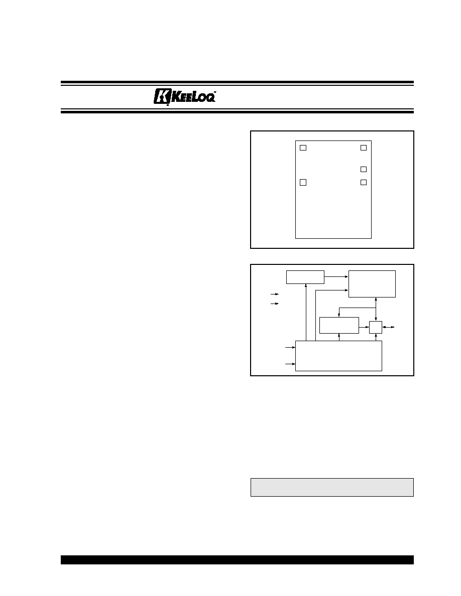
DIE LAYOUT
BLOCK DIAGRAM
A correct signature indicates that the memory contents
have not been altered. It can therefore be used to check
the serial number, or that changes to the token counter
have actually occurred.
Programming the token counter uses a special circuit to
ensure that the programming will either be complete or
will not happen at all, if the external supply is suddenly
removed.* This is called
Fail Safe ProgrammingTM
,
and, when used in conjunction with the extended write
and erase command, removes the need for special
`tear-out' protection to be performed by the reader.
Note:
The fail safe feature only works in the token
counter area.
GND
SDIO
V
DD
SCI
SCK
I/O
SCI
SCK
SDIO
V
DD
GND
ADDRESS
GENERATION
EEPROM
SIGNATURE
CALCULATOR
CONTROLLER
Token Card Chip
K
EE
L
OQ
is a registered trademark of Microchip Technology Inc.
*Patents applied for.

SCS152
DS40150B-page 2
Preliminary
©
1997 Microchip Technology Inc.
1.0
PIN DEFINITIONS
2.0
DEVICE OPERATION
During the life of the SCS152, it goes through the fol-
lowing stages:
∑ Manufacture and wafer probing
∑ Waffle pack and transportation
∑ Personalization and final application.
Various fields in the memory map must be initialized.
These include the first 24 bits in the memory map, the
transport code, and the mode bits. The first 24 bits in
the memory map typically identifies the device in its
final application. The device has two principle modes:
issuer mode and user mode. In issuer mode, all access
to the device (except one field) is blocked before a cor-
rect transport code has been presented to the device.
Thus, the transport code protects the device against
theft, before it is personalized.
During personalization, all fields, except (Chip
Identification Data (CID), are initialized for the intended
application: the device serial number is programmed,
the token counter is set to its proper value, the user
data field is initialized, and the transport code is erased
and replaced with a cryptographic key.
After power has been applied to the device, the I/O pin
is driven low. Once the reset period (T
POR
) has expired,
the SCS152 is ready to accept commands. These com-
mands typically read the memory content serially. The
first bit at address 0 is initially driven on the I/O line.
Each read clock pulse increments the internal address
counter and reads the resulting bit from EEPROM. This
serial data stream is composed of various fields pre-
sented in Table 2-1.
2.1
CID Field
The device CID field contains a device identification
code, which is programmed during wafer probe and
cannot be changed later. These bits typically identify
the type of the device to the system in the application.
2.2
SER Field
The SER field contains the device serial number which
identifies the individual device. It is programmed while
the device is in issuer mode during the personalization
stage.
2.3
ISS Field
The ISS field indicates whether the device is in issuer
mode as determined by the CFG field. This is purely an
external view of the CFG field and exists as such for
compatibility reasons.
ISO
Pin Name
I/O Type
Description
C1
V
DD
Power
Power connection
C2
SCI
INPUT
Command input to the device controller
C3
SCK
INPUT
Command execution clock input
C5
GND
Power
Power connection
C7
SDIO
Bidir (O.D.)
Open drain serial data I/O line
TABLE 2-1:
EXTERNAL
REPRESENTATION OF THE
INTERNAL MEMORY MAP
Field
Name
Address
Size
Description
CID
0...23
24
Chip identification
data
SER
24...63
40
Serial number
ISS
64
1
Issuer mode status
D4
65...71
7
Digit 4
D3
72...79
8
Digit 3
D2
80...87
8
Digit 2
D1
88...95
8
Digit 1
D0
96...103
8
Digit 0
CFG
104...107
4
Configuration data
USER0
108...147
40
User area
UKEY0
148...211
64
Key area 0 which
also acts as the
transport code in
issuer mode
212...275
64
Undefined

SCS152
©
1997 Microchip Technology Inc.
Preliminary
DS40150B-page 3
2.4
Digit Fields
2.4.1
DIGIT FIELD VALUE
Each digit field, D4 to D0, represents a number equal to
the number of `1' bits in the field. Table 2-2 shows the
value of the digit field for each legal digit value.
TABLE 2-2:
DIGIT FIELD VALUES
2.4.2
TOKEN COUNTER VALUE
The following formula shows how the digit fields combine to form the token counter value:
This is, in fact, an octal representation of a value and can be written as:
Suppose the 5-digit field contain the values: (D4=3), (D3=0), (D2=7), (D1=1), (D0=3). The token counter value is then
30713
8
in octal or in decimal:
A digit needs to be set to eight to handle the borrow from the next higher stage. This also implies that each counter value
does not have a unique representation. For example, 00500
8
= 5 x 64 = 320
10
or 00480
8
or 00478
8
.
Digit Value
Field Value
0
0000 0000
1
1000 0000
2
1100 0000
3
1110 0000
4
1111 0000
5
1111 1000
6
1111 1100
7
1111 1110
8
1111 1111
Note:
The bits are shown, right to left, in the order
in which they are read out.
Note:
The value digit D4 is shown in the formulas as |D4| indicating the number of 1 bits in the digit D4 field.
Similarly |D3| indicates the number of 1 bits in the digit D3 field, and so on.
Tokens
D4
4096
D3
512
D2
64
D1
8
D0
+
◊
+
◊
+
◊
+
◊
=
Tokens
D4
8
4
D3
8
3
D2
8
2
D1
8
1
D0
8
0
◊
+
◊
+
◊
+
◊
+
◊
=
Tokens
3
4096
0
512
7
64
1
8
3
+
◊
+
◊
+
◊
+
◊
12747
10
=
=

SCS152
DS40150B-page 4
Preliminary
©
1997 Microchip Technology Inc.
2.5
CFG Field
The CFG field is further divided into four subfields:
With `PC0 = 0' and `PC1 = 1', the device is in issuer
mode; with `PC0 = 1' and `PC1 = 0', the device is in user
mode. Some commands can only be used in issuer
mode.
2.6
USER0 Field
The user area can be reprogrammed to any state by the
user in user mode. It also can be locked using the
LOCK0 bit. In issuer mode, this field typically contains
the packaging status of the device. In user mode, this
field can be used for application dependent data.
2.7
UKEY0 Field
In issuer mode, this field contains the transport code; in
user mode, the UKEY0 field contains the key used in
the signature function. The transport code is
programmed during wafer probe and is completely
reprogrammed during personalization to the value of
the key.
3.0
COMMAND INTERFACE
The SCS152 accepts the following basic commands:
RESET, RDBIT/PUTBIT, BITPROG and ERASE. The
extended commands are DECR-ERASE and initiate
signature function.
The device interprets five different SCI/SCK sequences
for all its commands:
a)
An overlap of SCI and SCK for RESET
b)
A single pulse on SCK for RDBIT or PUTBIT
c)
A single pulse on SCI followed by a pulse on
SCK for BITPROG
d)
A repeat of c) for ERASE
e)
A double pulse on SCI followed by a pulse on
SCK for extended commands
Normally, any one of these sequences can be followed
by another; however, once the signature function has
been started, a fixed sequence of commands must fol-
low.
The extended functions are accessed by double pulse
on SCI in the correct address range. Depending on the
current address, the same sequence of events on SCI
and SCK will perform different functions.
Name
Address
Description
PC0
104
First bit of the issuer mode/user
mode indicator
PC1
105
Second bit of the issuer mode/
user mode indicator
N.U.
106
Unused
LOCK0
107
Unlocked status of USER0 area
in user mode: `0' means locked
TABLE 3-1:
EXTENDED FUNCTIONS
Field
Extended Function Accessed by
Double SCI Pulse
CID
Test modes
SER
BITPROG
D4...D0
DECR-ERASE
CFG
Test modes
USER0
BITPROG
UKEY0
Address 163: test mode
Address 259: Initiate signature operation
Other addresses perform BITPROG

SCS152
©
1997 Microchip Technology Inc.
Preliminary
DS40150B-page 5
3.1
Access Conditions
The condition codes are:
Note 1:
If the access condition does not allow a command that modifies the EEPROM (i.e., BITPROG, ERASE or
DECR-ERASE), it will be converted into a RDBIT command.
2:
The commands that can potentially change the EEPROM (even if it is converted into a RDBIT command) do
not increment the I/O address counter.
3:
Any command that modifies the EEPROM checks the internal high voltage sensor during the programming
and goes into the standby state if the sensor indicates the internal high voltage was not high enough. Power
must be removed to clear this condition.
4:
If the device is not in issuer mode and not in user mode, only BITPROG access is allowed to the CFG field.
TABLE 3-2:
ACCESS CONDITIONS IN ISSUER MODE
Field
RDBIT
BITPROG
ERASE
Extended Commands
CID
Y
F and TC
N
test modes
SER
Y
TC
N
BITPROG
O4...O1
Y
TC and Z
TC and B
DECR-ERASE: TC and Z
O0
Y
TC and Z
N
N
CFG
Y
TC
N
test modes
USER0
Y
Y
Y
BITPROG
UKEY0
`1'
TC
TC
BITPROG
test modes
SIGN: Y
TABLE 3-3:
ACCESS CONDITIONS IN USER MODE
Field
RDBIT
BITPROG
ERASE
Extended Commands
CID
Y
N
N
test modes
SER
Y
N
N
BITPROG
O4...O1
Y
Z
B
DECR-ERASE: Z
O0
Y
Z
N
N
CFG
Y
Y
N
test modes
USER0
Y
L
L
BITPROG
UKEY0
`1'
N
N
BITPROG
test modes
SIGN: Y
∑ Y
Command always allowed
∑ N
No access allowed and it is converted into a RDBIT command
∑ TC
Transport code must be submitted before the operation is allowed
∑ `1'
Output always logic high in this field
∑ F
Command allowed if the fuse is not blown
∑ Z
The digit code is nonzero
∑ B
Command allowed if previous operation was BITPROG and was successfully
∑ L
Command allowed if LOCK0 bit in the CFG field is `1'
∑ BITPROG
The BITPROG condition is checked and executed