Document Outline
- Features/Options
- General Description
- Key Timing Parameters
- 54-Pin TSOP II Pin Assignment
- General Description (continued)
- Table of Contents
- Functional Block Diagram, 4 Meg x 16
- Pin Descriptions
- Pin Descriptions (continued)
- SDRAM Interface Functional Description
- Initialization
- Register Definition
- Mode Register
- Burst Length
- Burst Type
- Figure 1, Mode Register Definition
- Table 1, Burst Definition
- CAS Latency
- Operating Mode
- WRITE Burst Mode
- Figure 2, CAS Latency
- Table 2, CAS Latency
- Commands
- Truth Table 1, SDRAM-Compatible Interface Commands and DQM Operation
- Commands
- Truth Table 2, Flash Memory Command Sequences
- COMMAND INHIBIT
- NO OPERATION (NOP)
- LOAD MODE REGISTER
- ACTIVE
- READ
- WRITE
- ACTIVE TERMINATE
- BURST TERMINATE
- LOAD COMMAND REGISTER (LCR)
- Operation
- Bank/Row Activation
- Figure 3, Activating a Specific Row in a Specific Bank
- Figure 4, Example: Meeting t RCD (MIN) When 2 < t RCD (MIN)/t CK <= 3
- READs
- Figure 5, READ Command
- Figure 6, CAS Latency
- Figure 7, Consecutive READ Bursts
- Figure 8, Random Read Accesses Within a Page
- Figure 9, READ to WRITE
- Figure 10, Terminating a READ Burst
- WRITEs
- ACTIVE TERMINATE
- Burst Read/Single Write
- Power-Down
- Slock Suspend
- Figure 11, WRITE Command
- Figure 12, WRITE to READ
- Figure 13, Power-Down
- Figure 14, Clock Suspend During READ Burst
- Truth Table 3 - CKE
- Truth Table 4 - Current State Bank n; Command to Bank n
- Truth Table 5 - Current State Bank n; Command to Bank m
- Flash Memory Functional Description
- Memory Architecture
- Protected Blocks
- Command Execution Logic (CEL)
- Internal State Machine (ISM)
- ISM Status Register
- Figure 15, Memory Address Map
- OUTPUT (READ) Operations
- Memory Array
- Status Register
- Device Configuration Registers
- INPUT Operations
- Command Execution
- Status Register
- Device Configuration
- Program Sequence
- Erase Sequence
- PROGRAM and ERASE NVMODE REGISTER
- Block Protect/Unprotect Sequence
- Device Protect Sequence
- Reset/Deep Power-Down Mode
- Error Handling
- PROGRAM/ERASE Cycle Endurance
- Table 3, Status Register Bit Definition
- Table 4, Device Configuration
- Table 5, Status Register Error Decode
- Self-Timed PROGRAM Sequence
- Complete PROGRAM Status-Check Sequence
- Self-Timed Block ERASE Sequence
- Complete Block ERASE Status-Check Sequence
- Block Protect Sequence
- Complete Block Status-Check Sequence
- Device Protect Sequence
- Block Unprotect Sequence
- Absolute Maximum Ratings
- Electrical Characteristics and Recommended DC Operating Conditions
- ICC Specifications and Conditions
- Capacitance
- Electrical Characteristics and Recommended AC Operating Conditions
- AC Functional Characteristics
- ERASE and PROGRAM Characteristics
- Timing diagrams
- Initialize and Load Mode Register
- Clock Suspend Mode
- READ
- Alternating Bank READ Accesses
- READ Ö Full-Page Burst
- READ Ö DQM Operation
- PROGRAM/ERASE, (Bank a Followed by READ to Bank b)
- PROGRAM/ERASE, (Bank a Followed by READ to Bank a)
- 54-Pin TSOP Tupe II (400 Mil) Package Drawing

1
4 Meg x 16 SyncFlash
©2001, Micron Technology, Inc.
MT28S4M16LC_6.p65 ≠ Rev. 6, Pub. 9/01
4 MEG x 16
SYNCFLASH MEMORY
PRODUCTS AND SPECIFICATIONS DISCUSSED HEREIN ARE SUBJECT TO CHANGE BY MICRON WITHOUT NOTICE.
SYNCFLASH
Æ
MEMORY
FEATURES
∑ 100 MHz SDRAM-compatible read timing
∑ Fully synchronous; all signals registered on
positive edge of system clock
∑ Internal pipelined operation; column address can
be changed every clock cycle
∑ Internal banks for hiding row access
∑ Programmable burst lengths: 1, 2, 4, 8, or full page
(READ)
∑ LVTTL-compatible inputs and outputs
∑ Single +3.3V ±0.3V power supply
≠ Additional V
HH
hardware protect mode (RP#)
∑ Four-bank architecture supports true concurrent
operations with zero latency:
Read from any bank while performing a
PROGRAM or ERASE operation to any other
bank
∑ Deep power-down mode: 300µA maximum
∑ Cross-compatible Flash memory command set
∑ Industry-standard, SDRAM-compatible pinouts
≠ Pins 36 and 40 are no connects for SDRAM
OPTIONS
MARKING
∑ Configuration
4 Meg x 16 (1 Meg x 16 x 4 banks)
4M16
∑ Read Timing (Cycle Time)
10ns (100 MHz)
-10
12ns (83 MHz)
-12
∑ Package
54-pin OCPL
1
TSOP II (400 mil)
TG
∑ Operating Temperature Range
Commercial Temperature (0∫C to +70∫C) None
NOTE: 1. Off-center parting line
Part Number Example:
MT28S4M16LCTG-10
PIN ASSIGNMENT (Top View)
MT28S4M16LC
1 Meg x 16 x 4 banks
54-Pin TSOP II
NOTE: The # symbol indicates signal is active LOW.
V
CC
DQ0
V
CC
Q
DQ1
DQ2
V
SS
Q
DQ3
DQ4
V
CC
Q
DQ5
DQ6
V
SS
Q
DQ7
V
CC
DQML
WE#
CAS#
RAS#
CS#
BA0
BA1
A10
A0
A1
A2
A3
V
CC
1
2
3
4
5
6
7
8
9
10
11
12
13
14
15
16
17
18
19
20
21
22
23
24
25
26
27
54
53
52
51
50
49
48
47
46
45
44
43
42
41
40
39
38
37
36
35
34
33
32
31
30
29
28
V
SS
DQ15
V
SS
Q
DQ14
DQ13
V
CC
Q
DQ12
DQ11
V
SS
Q
DQ10
DQ9
V
CC
Q
DQ8
V
SS
RP#
DQMH
CLK
CKE
V
CC
P
A11
A9
A8
A7
A6
A5
A4
V
SS
GENERAL DESCRIPTION
This SyncFlash
Æ
data sheet is divided into two ma-
jor sections. The SDRAM Interface Functional
Description details compatibility with the SDRAM
memory, and the Flash Memory Functional Descrip-
tion specifies the symmetrical-sectored flash architec-
ture functional commands.
KEY TIMING PARAMETERS
SPEED
CLOCK
ACCESS TIME
SETUP
HOLD
GRADE
FREQUENCY CL = 2* CL = 3*
TIME
TIME
-10
100 MHz
≠
7ns
3ns
2ns
-10
66 MHz
9ns
≠
3ns
2ns
-12
83 MHz
≠
9ns
3ns
2ns
-12
66 MHz
10ns
≠
3ns
2ns
*CL = CAS (READ) latency
The MT28S4M16LC is a nonvolatile, electrically sec-
tor-erasable (Flash), programmable memory contain-
ing 67,108,864 bits organized as 4,194,304 words (16
bits). SyncFlash memory is ideal for 3.3V-only plat-
forms that require both hardware and software protec-
tion modes. Additional hardware protection modes are

2
4 Meg x 16 SyncFlash
Micron Technology, Inc., reserves the right to change products or specifications without notice.
MT28S4M16LC_6.p65 ≠ Rev. 6, Pub. 9/01
©2001, Micron Technology, Inc.
4 MEG x 16
SYNCFLASH MEMORY
GENERAL DESCRIPTION (continued)
also available when V
HH
is applied to the RP# pin. Pro-
gramming or erasing the device is done with a 3.3V
V
CC
P voltage, while all other operations are performed
with a 3.3V V
CC
. The device is fabricated with Micron's
advanced CMOS floating-gate process.
The MT28S4M16LC is organized into 16 indepen-
dently erasable blocks. To ensure that critical firmware
is protected from accidental erasure or overwrite, the
MT28S4M16LC features sixteen 256K-word hardware-
and software-lockable blocks.
The MT28S4M16LC four-bank architecture supports
true concurrent operations. A read access to any bank
can occur simultaneously with a background PRO-
GRAM or ERASE operation to any other bank.
The SyncFlash memory has a synchronous inter-
face (all signals are registered on the positive edge of
the clock signal, CLK). Read accesses to the memory are
burst oriented; accesses start at a selected location and
continue for a programmed number of locations in a
programmed sequence. Accesses begin with the regis-
tration of an ACTIVE command, followed by a READ
command. The address bits registered coincident with
the ACTIVE command are used to select the bank and
row to be accessed. The address bits registered coinci-
dent with the READ command are used to select the
starting column location for the burst access.
The SyncFlash memory provides for programmable
read burst lengths of 1, 2, 4, or 8 locations, or the full
page, with a burst terminate option.
The 4 Meg x 16 SyncFlash memory uses an internal
pipelined architecture to achieve high-speed
operation.
The 4 Meg x 16 SyncFlash memory is designed to
operate in 3.3V, low-power memory systems. A deep
power-down mode is provided, along with a power-
saving standby mode. All inputs and outputs are
LVTTL-compatible.
SyncFlash memory offers substantial advances in
Flash operating performance, including the ability to
synchronously burst data at a high data rate with auto-
matic column-address generation and the capability
to randomly change column addresses on each clock
cycle during a burst access.
Please refer to Micron's Web site (
www.micron.com/
flash
) for the latest data sheet.

3
4 Meg x 16 SyncFlash
Micron Technology, Inc., reserves the right to change products or specifications without notice.
MT28S4M16LC_6.p65 ≠ Rev. 6, Pub. 9/01
©2001, Micron Technology, Inc.
4 MEG x 16
SYNCFLASH MEMORY
TABLE OF CONTENTS
Functional Block Diagram ≠ 4 Meg x 16 ...............
4
Pin Descriptions ......................................................
5
SDRAM Interface Functional Description ..........
7
Initialization ......................................................
7
Register Definition ............................................
7
Mode Register ...............................................
7
Burst Length ............................................
7
Burst Type ...............................................
7
CAS Latency ............................................
9
Operating Mode ......................................
9
Write Burst Mode ....................................
9
Commands ........................................................ 10
Truth Table 1 (Commands and DQM Operation) .......
10
Truth Table 2 (Commands Sequences) .......................
11
Command Inhibit ........................................ 13
No Operation (NOP) .................................... 13
Load Mode Register ...................................... 13
Active ............................................................ 13
Read .............................................................. 13
Write ............................................................. 13
Active Terminate .......................................... 13
Burst Terminate ............................................ 13
Load Command Register ............................. 13
Operation .......................................................... 14
Bank/Row Activation .................................. 14
Reads ............................................................ 15
Writes ........................................................... 20
Active Terminate .......................................... 20
Power-Down ................................................ 20
Clock Suspend ............................................. 20
Burst Read/Single Write ............................... 21
Truth Table 3 (CKE) ..................................................
21
Truth Table 4 (Current State, Same Bank) ..................
22
Truth Table 5 (Current State, Different Bank) .............
23
Flash Memory Functional Description ............... 24
Command Interface .................................... 24
Memory Architecture ................................... 24
Protected Blocks ........................................... 24
Command Execution Logic (CEL) ............... 25
Internal State Machine (ISM) ...................... 25
ISM Status Register ...................................... 25
Output (READ) Operations .............................. 25
Memory Array ............................................. 25
Status Register .............................................. 25
Device Configuration Registers ................... 25
Input Operations .............................................. 26
Memory Array ............................................. 26
Command Execution ........................................ 26
Status Register .............................................. 27
Device Configuration .................................. 27
Program Sequence ....................................... 27
Erase Sequence ............................................. 27
Program and Erase NVMode Register ......... 27
Block Protect/Unprotect Sequence .............. 27
Device Protect Sequence .............................. 28
Reset/Deep Power-Down Mode ....................... 28
Error Handling .................................................. 28
PROGRAM/ERASE Cycle Endurance ................ 28
Absolute Maximum Ratings .................................. 35
DC Electrical Characteristics
and Operating Conditions ................................... 35
I
CC
Specifications and Conditions .......................... 36
Capacitance ............................................................ 36
Electrical Characteristics and Recommended
Operating Conditions (Timing Table) ............. 37
AC Functional Characteristics ............................. 38
Notes ...................................................................... 39
Timing Waveforms
Initialize and Load Mode Register ..................... 40
Clock Suspend Mode ......................................... 41
Reads
Read .............................................................. 42
Alternating Bank Read Accesses ................... 43
Read ≠ Full-Page Burst ................................. 44
Read ≠ DQM Operation .............................. 45
Program
Program/Erase
(Bank a followed by READ to bank b) .. 46
Program/Erase
(Bank a followed by READ to bank a) .. 47
4
4 Meg x 16 SyncFlash
Micron Technology, Inc., reserves the right to change products or specifications without notice.
MT28S4M16LC_6.p65 ≠ Rev. 6, Pub. 9/01
©2001, Micron Technology, Inc.
4 MEG x 16
SYNCFLASH MEMORY
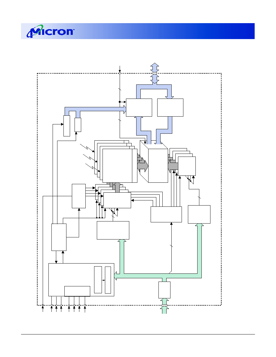
FUNCTIONAL BLOCK DIAGRAM
4 Meg x 16
RAS#
CAS#
ROW-
ADDRESS
MUX
CLK
CS#
WE#
CKE
COLUMN-
ADDRESS
COUNTER/
LATCH
8
A0≠A11,
BA0, BA1
DQML,
DQMH
12
ADDRESS
REGISTER
14
256
(x16)
4,096
I/O GATING
DQM MASK LOGIC
READ DATA LATCH
WRITE DRIVERS
COLUMN
DECODER
BANK 0
MEMORY
ARRAY
(4,096 x 256 x 16)
BANK 0
ROW-
ADDRESS
LATCH
&
DECODER
High Voltage
Switch/Pump
4,096
SENSE AMPLIFIERS
BANK
CONTROL
LOGIC
DQ0≠DQ15
16
16
16
12
BANK 1
BANK 2
BANK 3
12
8
2
2
2
COMMAND
EXECUTION
LOGIC
MODE REGISTER
COMMAND
DECODE
STATE MACHINE
STATUS REG.
NVMODE
REGISTER
16
DATA
INPUT
REGISTER
DATA
OUTPUT
REGISTER
RP#
V
CC
P
ID REG.

5
4 Meg x 16 SyncFlash
Micron Technology, Inc., reserves the right to change products or specifications without notice.
MT28S4M16LC_6.p65 ≠ Rev. 6, Pub. 9/01
©2001, Micron Technology, Inc.
4 MEG x 16
SYNCFLASH MEMORY
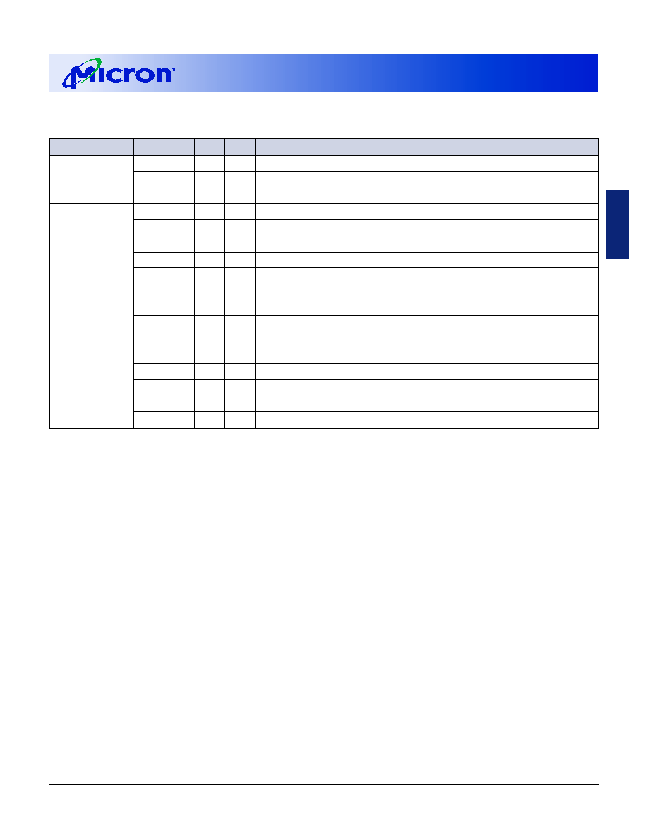
PIN DESCRIPTIONS
54-PIN TSOP
NUMBERS
SYMBOL
TYPE
DESCRIPTION
38
CLK
Input
Clock: CLK is driven by the system clock. All SyncFlash memory input
signals are sampled on the positive edge of CLK. CLK also increments
the internal burst counter and controls the output registers.
37
CKE
Input
Clock Enable: CKE activates (HIGH) and deactivates (LOW) the CLK
signal. Deactivating the clock provides STANDBY operation or CLOCK
SUSPEND operation (burst/access in progress). CKE is synchronous
except after the device enters power-down modes, where CKE
becomes asynchronous until after exiting the same mode. The input
buffers, including CLK, are disabled during power-down modes,
providing low standby power. CKE may be tied HIGH in systems where
power-down modes (other than RP# deep power-down) are not
required.
19
CS#
Input
Chip Select: CS# enables (registered LOW) and disables (registered
HIGH) the command decoder. All commands are masked when CS# is
registered HIGH. CS# provides for external bank selection on systems
with multiple banks. CS# is considered part of the command code.
18, 17, 16
RAS#,
Input
Command Inputs: RAS#, CAS#, and WE# (along with CS#) define the
CAS#,
command being entered.
WE#
15, 39
DQML,
Input
Input/Output Mask: DQM is an input mask signal for write accesses
DQMH
and an output enable signal for read accesses. Input data is masked
when DQM is sampled HIGH during a WRITE cycle. The output buffers
are placed in a High-Z state (after a two-clock latency) when DQM is
sampled HIGH during a READ cycle. DQML corresponds to DQ0≠DQ7
and DQMH corresponds to DQ8≠DQ15. DQML and DQMH are
considered same state when referenced as DQM.
23-26, 29-34,
A0≠A11
Input
Address Inputs: A0≠A11 are sampled during the ACTIVE command
22, 35
(row-address A0≠A11) and READ/WRITE command (column-address
A0≠A7) to select one location in the respective bank. The address
inputs provide the Op-Code during LOAD MODE REGISTER command
and the operation code during a LOAD COMMAND REGISTER
command.
40
RP#
Input
Initialize/Power-Down: Upon initial device power-up, a 100µs delay
after RP# has transitioned from LOW to HIGH is required for internal
device initialization, prior to issuing an executable command. RP#
clears the status register, sets the internal state machine (ISM) to the
array read mode, and places the device in the deep power-down
mode when LOW. All inputs, including CS#, are "Don't Care" and all
outputs are High-Z. When RP# = V
HH
, all protection modes are ignored
during PROGRAM and ERASE. Also allows the device protect bit to be
set to "1" (protected) and allows the block protect bits at locations 0
and 15 to be set to "0" (unprotected) when brought to V
HH
. RP# must
be held HIGH during all other modes of operation.
(continued on next page)

6
4 Meg x 16 SyncFlash
Micron Technology, Inc., reserves the right to change products or specifications without notice.
MT28S4M16LC_6.p65 ≠ Rev. 6, Pub. 9/01
©2001, Micron Technology, Inc.
4 MEG x 16
SYNCFLASH MEMORY
20, 21
BA0,
Input
Bank Address Input(s): BA0, BA1 define to which bank the command
BA1
is being applied. See Truth Tables 1 and 2.
2, 4, 5, 7, 8, 10,
DQ0-
I/O
Data I/O: Data bus.
11,13, 42, 44, 45,
DQ15
47, 48, 50, 51, 53
3, 9, 43, 49
V
CC
Q
Supply
DQ Power: Provide isolated power to DQs for improved noise
immunity.
6, 12, 46, 52
V
SS
Q
Supply
DQ Ground: Provide isolated ground to DQs for improved noise
immunity.
1, 14, 27
V
CC
Supply
Power Supply: 3.3V ±0.3V.
28, 41, 54
V
SS
Supply
Ground.
36
V
CC
P
Supply
Program/Erase Supply Voltage: V
CC
P must be tied externally to V
CC
. The
V
CC
P pin sources current during device initialization, PROGRAM and
ERASE operations.
PIN DESCRIPTIONS (continued)
54-PIN TSOP
NUMBERS
SYMBOL
TYPE
DESCRIPTION

7
4 Meg x 16 SyncFlash
Micron Technology, Inc., reserves the right to change products or specifications without notice.
MT28S4M16LC_6.p65 ≠ Rev. 6, Pub. 9/01
©2001, Micron Technology, Inc.
4 MEG x 16
SYNCFLASH MEMORY
SDRAM
SDRAM INTERFACE
FUNCTIONAL DESCRIPTION
In general, the 64Mb SyncFlash memory (1 Meg x 16
x 4 banks) is configured as a quad-bank, nonvolatile
SDRAM that operates at 3.3V and includes a synchro-
nous interface (all signals are registered on the positive
edge of the clock signal, CLK). Each of the x16's
16,777,216-bit banks is organized as 4,096 rows by 256
columns by 16 bits.
Read accesses to the SyncFlash memory are burst
oriented; accesses start at a selected location and con-
tinue for a programmed number of locations in a pro-
grammed sequence. Accesses begin with the registra-
tion of an ACTIVE command, followed by a READ com-
mand. The address bits registered coincident with the
ACTIVE command are used to select the bank and row
to be accessed (BA0 and BA1 select the bank, A0≠A11
select the row). The address bits registered coincident
with the READ command are used to select the starting
column location for the burst access (BA0 and BA1 se-
lect the bank, A0≠A7 select the column).
Prior to normal operation, the SyncFlash memory
must be initialized. The following sections provide de-
tailed information covering device initialization, regis-
ter definition, command descriptions, and device op-
eration.
Initialization
SyncFlash memory must be powered up and initial-
ized in a predefined manner. Operational procedures
other than those specified may result in undefined
operation. After power is applied to V
CC
, V
CC
Q, and V
CC
P
(simultaneously), and the clock is stable, RP# must be
brought from LOW to HIGH. A 100µs delay is required
after RP# transitions HIGH in order to complete inter-
nal device initialization.
The SyncFlash memory is now in the array read mode
and ready for mode register programming or an ex-
ecutable command. After initial programming of the
nvmode register, the contents are automatically loaded
into the mode register during initialization and the
device will power up in the programmed state.
Register Definition
MODE REGISTER
The mode register is used to define the specific mode
of operation of the SyncFlash memory. This definition
includes the selection of a burst length, a burst type, a
CAS latency, and an operating mode, as shown in Fig-
ure 1. The mode register is programmed via the LOAD
MODE REGISTER command and will retain the stored
information until it is reprogrammed. The contents of
the mode register may be copied into the nvmode reg-
ister; the mode register settings automatically load the
mode register during initialization. Details on erase
nvmode register and program nvmode register com-
mand sequences are found in the Command Execu-
tion section of the Flash Memory Functional Descrip-
tion.
Mode register bits M0≠M2 specify the burst length,
M3 specifies the burst type (sequential or interleaved),
M4≠M6 specify the CAS latency, M7 and M8 specify the
operating mode, M9 specifies the write burst mode in
an SDRAM (M9 = 1 by default), and M10 and M11 are
reserved for future use.
The mode register must be loaded when all banks
are idle, and the controller must wait the specified time
before initiating the subsequent operation. Violating
either of these requirements will result in unspecified
operation.
BURST LENGTH
Read accesses to the SyncFlash memory are burst
oriented, with the burst length being programmable,
as shown in Figure 1. The burst length determines the
maximum number of column locations that can be ac-
cessed for a given READ command. Burst lengths of 1,
2, 4, or 8 locations are available for both sequential and
interleaved burst types, and a full-page burst is avail-
able for the sequential type. The full-page burst is
used in conjunction with the BURST TERMINATE com-
mand to generate arbitrary burst lengths.
Reserved states should not be used, as unknown
operation or incompatibility with future versions may
result.
When a READ command is issued, a block of col-
umns equal to the burst length is effectively selected.
All accesses for that burst take place within this block,
meaning that the burst will wrap within the block if a
boundary is reached. The block is uniquely selected by
A1≠A7 when the burst length is set to two, by A2≠A7
when the burst length is set to four, and by A3≠A7 when
the burst length is set to eight. The remaining (least
significant) address bit(s) are used to select the start-
ing location within the block. Full-page bursts wrap
within the page if the boundary is reached.
BURST TYPE
Accesses within a given burst may be programmed
to be either sequential or interleaved; this is referred to
as the burst type and is selected via bit M3.
The ordering of accesses within a burst is deter-
mined by the burst length, the burst type, and the
starting column address, as shown in Table 1.

8
4 Meg x 16 SyncFlash
Micron Technology, Inc., reserves the right to change products or specifications without notice.
MT28S4M16LC_6.p65 ≠ Rev. 6, Pub. 9/01
©2001, Micron Technology, Inc.
4 MEG x 16
SYNCFLASH MEMORY
SDRAM
Figure 1
Mode Register Definition
Table 1
Burst Definition
Burst
Starting Column
Order of Accesses Within a Burst
Length
Address
Type = Sequential
Type = Interleaved
A0
2
0
0-1
0-1
1
1-0
1-0
A1 A0
0
0
0-1-2-3
0-1-2-3
4
0
1
1-2-3-0
1-0-3-2
1
0
2-3-0-1
2-3-0-1
1
1
3-0-1-2
3-2-1-0
A2 A1 A0
0
0
0
0-1-2-3-4-5-6-7
0-1-2-3-4-5-6-7
0
0
1
1-2-3-4-5-6-7-0
1-0-3-2-5-4-7-6
0
1
0
2-3-4-5-6-7-0-1
2-3-0-1-6-7-4-5
8
0
1
1
3-4-5-6-7-0-1-2
3-2-1-0-7-6-5-4
1
0
0
4-5-6-7-0-1-2-3
4-5-6-7-0-1-2-3
1
0
1
5-6-7-0-1-2-3-4
5-4-7-6-1-0-3-2
1
1
0
6-7-0-1-2-3-4-5
6-7-4-5-2-3-0-1
1
1
1
7-0-1-2-3-4-5-6
7-6-5-4-3-2-1-0
Full
n = A0≠A7
Cn, Cn+1, Cn+2
Page
Cn+3, Cn+4...
Not supported
256
(location 0-255)
...Cn-1,
Cn...
NOTE: 1. For a burst length of two, A1≠A7 select the block-
of-two burst; A0 selects the starting column
within the block.
2. For a burst length of four, A2≠A7 select the block-
of-four burst; A0≠A1 select the starting column
within the block.
3. For a burst length of eight, A3≠A7 select the
block-of-eight burst; A0≠A2 select the starting
column within the block.
4. For a full-page burst, the full row is selected and
A0≠A7 select the starting column.
5. Whenever a boundary of the block is reached
within a given sequence above, the following
access wraps within the block.
6. For a burst length of one, A0≠A7 select the unique
column to be accessed, and mode register bit M3
is ignored.
M2
0
0
0
0
1
1
1
1
M1
0
0
1
1
0
0
1
1
M0
0
1
0
1
0
1
0
1
M3 = 0
1
2
4
8
Reserved
Reserved
Reserved
Full Page
M3 = 1
1
2
4
8
Reserved
Reserved
Reserved
Reserved
Operating Mode
Standard Operation
All other states reserved
0
-
0
-
Defined
-
0
1
Burst Type
Sequential
Interleaved
CAS Latency
Reserved
1
2
3
Reserved
Reserved
Reserved
Reserved
M6
0
0
0
0
1
1
1
1
M4
0
1
0
1
0
1
0
1
M5
0
0
1
1
0
0
1
1
Burst Length
Burst Length
CAS Latency
BT
A9
A7
A6
A5
A4
A3
A8
A2
A1
A0
Mode Register (Mx)
Address Bus
9
7
6
5
4
3
8
2
1
0
M3
M6-M0
M8
M7
Op Mode
A10
A11
10
11
Reserved* WB
0
1
Write Burst Mode
Reserved
Single Location Access
M9
*Program
M11, M10 = 0, 0
to ensure compatibility
with future devices.

9
4 Meg x 16 SyncFlash
Micron Technology, Inc., reserves the right to change products or specifications without notice.
MT28S4M16LC_6.p65 ≠ Rev. 6, Pub. 9/01
©2001, Micron Technology, Inc.
4 MEG x 16
SYNCFLASH MEMORY
SDRAM
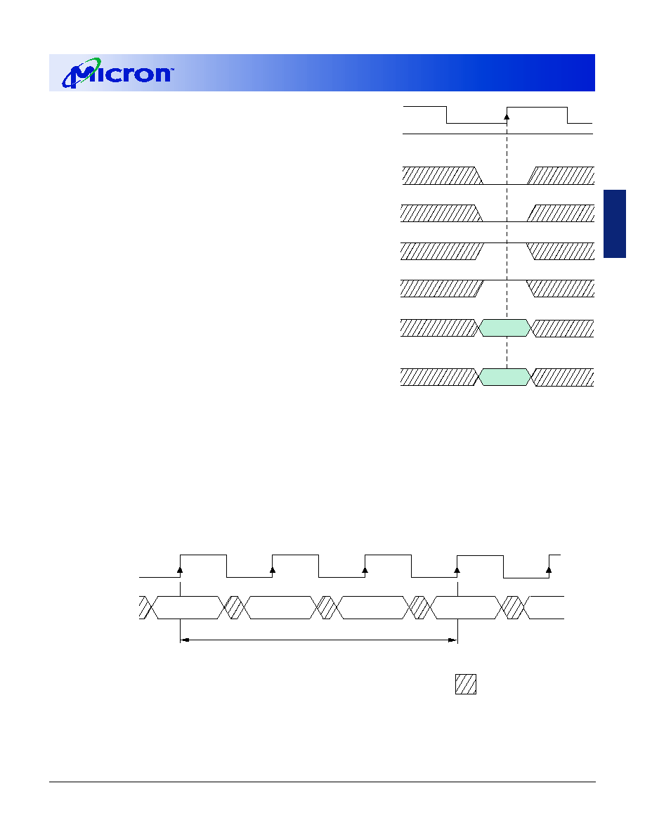
CAS LATENCY
The CAS latency is the delay, in clock cycles, be-
tween the registration of a READ command and the
availability of the first piece of output data. The la-
tency can be set to one, two, or three clocks.
If a READ command is registered at clock edge n,
and the latency is m clocks, the data will be available by
Figure 2
CAS Latency
Table 2
CAS Latency
ALLOWABLE OPERATING
FREQUENCY (MHz)
CAS
CAS
CAS
SPEED
LATENCY = 1 LATENCY = 2 LATENCY = 3
-10
33
66
100
-12
33
66
83
clock edge n + m. The DQs will start driving as a result of
the clock edge one cycle earlier (n + m - 1) and, provided
that the relevant access times are met, the data will be
valid by clock edge n + m. For example, assuming that
the clock cycle time is such that all relevant access times
are met, if a READ command is registered at T0, and the
latency is programmed to two clocks, the DQs will start
driving after T1 and the data will be valid by T2, as
shown in Figure 2. Table 2 below indicates the operat-
ing frequencies at which each CAS latency setting can
be used.
Reserved states should not be used, as unknown
operation or incompatibility with future versions may
result.
OPERATING MODE
The normal operating mode is selected by setting
M7 and M8 to zero; the other combinations of values for
M7 and M8 are reserved for future use and/or test
modes. The programmed burst length applies to READ
bursts.
Test modes and reserved states should not be used
because unknown operation or incompatibility with
future versions may result.
WRITE BURST MODE
WRITE bursts are not supported with the
MT28S4M16LC. By default, M9 is set to "1" and write
accesses are single-location (nonburst) accesses.
CLK
DQ
T2
T1
T3
T0
CAS Latency = 3
LZ
D
OUT
tOH
t
COMMAND
NOP
READ
tAC
NOP
T4
NOP
DON'T CARE
UNDEFINED
CLK
DQ
T2
T1
T0
CAS Latency = 1
LZ
D
OUT
tOH
t
COMMAND
NOP
READ
tAC
CLK
DQ
T2
T1
T3
T0
CAS Latency = 2
LZ
D
OUT
tOH
t
COMMAND
NOP
READ
tAC
NOP
10
4 Meg x 16 SyncFlash
Micron Technology, Inc., reserves the right to change products or specifications without notice.
MT28S4M16LC_6.p65 ≠ Rev. 6, Pub. 9/01
©2001, Micron Technology, Inc.
4 MEG x 16
SYNCFLASH MEMORY
SDRAM
COMMANDS
Truth Table 1 provides a quick reference of avail-
able commands for SDRAM-compatible operation. This
is followed by a written description of each command.
Additional truth tables appear later.
TRUTH TABLE 1
SDRAM-COMPATIBLE INTERFACE COMMANDS AND DQM OPERATION
(Notes: 1)
NAME (FUNCTION)
CS#
RAS# CAS# WE# DQM
ADDR
D Q s NOTES
COMMAND INHIBIT (NOP)
H
X
X
X
X
X
X
NO OPERATION (NOP)
L
H
H
H
X
X
X
ACTIVE (Select bank and activate row)
L
L
H
H
X
Bank/Row
X
2
READ (Select bank, column and start READ burst)
L
H
L
H
X
Bank/Col
X
3
WRITE (Select bank, column and start WRITE)
L
H
L
L
X
Bank/Col
Valid
3, 4
BURST TERMINATE
L
H
H
L
X
X
Active
ACTIVE TERMINATE
L
L
H
L
X
X
X
5
LOAD COMMAND REGISTER
L
L
L
H
X
ComCode
X
6, 7
LOAD MODE REGISTER
L
L
L
L
X
OpCode
X
8
Write Enable/Output Enable
≠
≠
≠
≠
L
≠
Active
9
Write Inhibit/Output High-Z
≠
≠
≠
≠
H
≠
High-Z
9
NOTE: 1. CKE is HIGH for all commands shown.
2. A0≠A11 provide row address, and BA0 and BA1 determine which bank is made active.
3. A0≠A7 provide column address, and BA0 and BA1 determine which bank is being read from or written to.
4. A program setup command sequence (see Truth Table 2) must be completed prior to executing a WRITE.
5. ACTIVE TERMINATE is functionally equivalent to the SDRAM PRECHARGE command, however PRECHARGE (deactivate row
in bank or banks) is not required for SyncFlash memory. A10 LOW: BA0 and BA1 determine the bank being active
terminated. A10 HIGH: All banks active terminated and BA0 and BA1 are "Don't Care."
6. A0≠A7 define the ComCode, and A8≠A11 are "Don't Care" for this operation. See Truth Table 2.
7. LOAD COMMAND REGISTER (LCR) replaces the SDRAM AUTO REFRESH or SELF REFRESH command, which is not required
for SyncFlash memory. LCR is the first cycle for Flash memory command sequences. See Truth Table 2.
8. A0≠A11 define the OpCode written to the mode register. The mode register can be dynamically loaded each cycle,
provided
t
MRD is satisfied. The contents of the nvmode register are automatically loaded into the mode register during
device initialization.
9. Activates or deactivates the DQs during WRITEs (zero-clock delay) and READs (two-clock delay).
11
4 Meg x 16 SyncFlash
Micron Technology, Inc., reserves the right to change products or specifications without notice.
MT28S4M16LC_6.p65 ≠ Rev. 6, Pub. 9/01
©2001, Micron Technology, Inc.
4 MEG x 16
SYNCFLASH MEMORY
SDRAM
COMMANDS
Truth Table 2 provides a quick reference of available commands
for flash memory interface operation. A written description of each
command is found in the Flash Memory Functional Description sec-
tion.
TRUTH TABLE 2
FLASH MEMORY COMMAND SEQUENCES
(Notes: 1, 2, 3, 4, 5; see notes on the next page.)
FIRST CYCLE
SECOND CYCLE
THIRD CYCLE
BANK
BANK
BANK
OPERATION
CMD
ADDR
6
ADDR
DQ
RP#
CMD
7
ADDR ADDR
DQ
RP#
CMD
ADDR ADDR
DQ
8
RP#
NOTES
READ DEVICE CONFIGURATION
LCR
90h
Bank
X
H
ACTIVE
Row
Bank
X
H
READ
CA
Bank
X
H
9, 10
READ STATUS REGISTER
LCR
70h
X
X
H
ACTIVE
X
X
X
H
READ
X
X
X
H
CLEAR STATUS REGISTER
LCR
50h
X
X
H
ERASE SETUP/CONFIRM
LCR
20h
Bank
X
H
ACTIVE
Row
Bank
X
H
WRITE
X
Bank
D0h
H/V
HH
11, 12, 13
PROGRAM SETUP/PROGRAM
LCR
40h
Bank
X
H
ACTIVE
Row
Bank
X
H
WRITE
Col
Bank
D
IN
H/V
HH
11, 12, 13
PROTECT BLOCK/CONFIRM
LCR
60h
Bank
X
H
ACTIVE
Row
Bank
X
H
WRITE
X
Bank
01h
H/V
HH
11, 12,
13, 14
PROTECT DEVICE/CONFIRM
LCR
60h
Bank
X
H
ACTIVE
X
Bank
X
H
WRITE
X
Bank
F1h
V
HH
11, 12
UNPROTECT BLOCKS/CONFIRM
LCR
60h
Bank
X
H
ACTIVE
X
Bank
X
H
WRITE
X
Bank
D0h
H/V
HH
11, 12,
13, 15
ERASE NVMODE REGISTER
LCR
30h
Bank
X
H
ACTIVE
X
Bank
X
H
WRITE
X
Bank
C0h
H
11, 12
PROGRAM NVMODE REGISTER
LCR
A0h
Bank
X
H
ACTIVE
X
Bank
X
H
WRITE
X
Bank
X
H
11, 12

12
4 Meg x 16 SyncFlash
Micron Technology, Inc., reserves the right to change products or specifications without notice.
MT28S4M16LC_6.p65 ≠ Rev. 6, Pub. 9/01
©2001, Micron Technology, Inc.
4 MEG x 16
SYNCFLASH MEMORY
SDRAM
NOTE: 1. CMD = Command: Decoded from CS#, RAS#, CAS#, and WE# inputs.
2. NOP/COMMAND INHIBIT commands may be issued throughout any operation command sequence.
3. After a PROGRAM or ERASE operation is registered to the ISM and prior to completion of the ISM operation, a READ to
any location in the bank under ISM control will output the contents of the row activated prior to the LCR/active/write
sequence (see Note 7).
4. In order to meet the
t
RCD specification, the appropriate number of NOP/COMMAND INHIBIT commands must be issued
between ACTIVE and READ/WRITE commands.
5. The ERASE, PROGRAM, PROTECT, UNPROTECT operations are self-timed. The status register may be polled to monitor
these operations.
6. A8≠A11 are "Don't Care."
7. A row will not be opened when ACTIVE is preceded by LCR. ACTIVE is considered a NOP.
8. Data Inputs: DQ8≠DQ15 are "Don't Care."
Data Outputs: All unused bits are driven LOW.
9. The block address is required during ACTIVE and READ cycles for the block protect bit location. The first row in a block
should be specified, acceptable values include 000h, 400h, 800h, and C00h. Bank address is "Don't Care" for manufac-
turer compatibility ID, device ID, and device protect bit location.
10. CA = Configuration Address:
000h ≠ Manufacturer compatibility ID (2Ch)
001h ≠ Device ID (D3h)
x02h ≠ Block protect bit, where x = 0, 4, 8, or Ch
003h ≠ Device protect bit
11. The proper command sequence (LCR/active/write) is needed to initiate an ERASE, PROGRAM, PROTECT, UNPROTECT
operation.
12. The bank address must match for the three command cycles (LCR/ACTIVE/WRITE) to initiate an ERASE, PROGRAM,
PROTECT, UNPROTECT operation.
13. If the device protect bit is set, then an ERASE, PROGRAM, PROTECT, UNPROTECT operation can still be initiated by
bringing RP# to V
HH
prior to the WRITE command cycle and holding it at V
HH
until the operation is completed.
14. The A10, A11 row address and BA0, BA1 bank address select the block to be protected; A0≠A9 are "Don't Care."
15. If the device protect bit is not set, RP# = V
IH
unprotects all sixteen 256K-word erasable blocks, except for blocks 0 and
15. When RP# = V
HH
, all sixteen 256K-word erasable blocks (including block 0 and 15) will be unprotected, and the
device protect bit will be ignored. If the device protect bit is set and RP# = V
IH
, the block protect bits cannot be
modified.

13
4 Meg x 16 SyncFlash
Micron Technology, Inc., reserves the right to change products or specifications without notice.
MT28S4M16LC_6.p65 ≠ Rev. 6, Pub. 9/01
©2001, Micron Technology, Inc.
4 MEG x 16
SYNCFLASH MEMORY
SDRAM
COMMAND INHIBIT
The COMMAND INHIBIT function prevents new
commands from being executed by the SyncFlash
memory, regardless of whether the CLK signal is en-
abled. The SyncFlash memory is effectively deselected.
Operations already in progress are not affected.
NO OPERATION (NOP)
The NO OPERATION (NOP) command is used to
perform a NOP to a SyncFlash memory that is selected
(CS# is LOW). This prevents unwanted commands from
being registered during idle or wait states. Operations
already in progress are not affected.
LOAD MODE REGISTER
The mode register is loaded via inputs A0≠A11 and
BA0 and BA1. See mode register heading in Register
Definition section. The LOAD MODE REGISTER com-
mand can only be issued when all banks are idle, and a
subsequent executable command cannot be issued
until
t
MRD is met. The data in the nvmode register is
automatically loaded into the mode register upon
power-up initialization and is the default mode setting
unless dynamically changed with the LOAD MODE
REGISTER command.
ACTIVE
The ACTIVE command is used to open (or activate)
a row in a particular bank for a subsequent access. The
value on the BA0, BA1 inputs selects the bank, and the
address provided on inputs A0≠A11 selects the row.
This row remains active for accesses until the next AC-
TIVE command, power-down or RESET.
READ
The READ command is used to initiate a burst read
access to an active row. The value on the BA0, BA1
inputs selects the bank, and the address provided on
inputs A0≠A7 selects the starting column location. Read
data appears on the DQs subject to the logic level on
the DQM input two clocks earlier. If a given DQM signal
was registered HIGH, the corresponding DQs will be
High-Z two clocks later; if the DQM signal was regis-
tered LOW, the DQs will provide valid data.
WRITE
The WRITE command is used to initiate a single-
location write access. A WRITE command must be pre-
ceded by LRC/ACTIVE. The value on the BA0, BA1 in-
puts selects the bank, and the address provided on
inputs A0≠A7 selects the column location.
Input data appearing on the DQs is written to the
memory array, subject to the DQM input logic level
appearing coincident with the data. If a given DQM
signal is registered LOW, the corresponding data will
be written to memory; if the DQM signal is registered
HIGH, the corresponding data inputs will be ignored,
and a WRITE will not be executed to that word/column
location. A WRITE command with DQM HIGH is con-
sidered a NOP.
ACTIVE TERMINATE
ACTIVE TERMINATE, which replaces the SDRAM
PRECHARGE command, is not required for SyncFlash
memory, but is functionally equivalent to the SDRAM
PRECHARGE command. ACTIVE TERMINATE can be
issued to terminate a BURST READ in progress and
may or may not be bank specific.
BURST TERMINATE
The BURST TERMINATE command is used to trun-
cate either fixed-length or full-page bursts. The most
recently registered READ command prior to the BURST
TERMINATE command will be truncated as shown in
the Operation section of this data sheet. BURST TER-
MINATE is not bank specific.
LOAD COMMAND REGISTER (LCR)
The LOAD COMMAND REGISTER (LCR) command
is used to initiate flash memory control commands to
the command execution logic (CEL). The CEL receives
and interprets commands to the device. These com-
mands control the operation of the ISM and the read
path (i.e., memory array, ID register, or status register).
However, there are restrictions on what commands are
allowed in this condition. See the Command Execution
section of Flash Memory Functional Description for
more details.
14
4 Meg x 16 SyncFlash
Micron Technology, Inc., reserves the right to change products or specifications without notice.
MT28S4M16LC_6.p65 ≠ Rev. 6, Pub. 9/01
©2001, Micron Technology, Inc.
4 MEG x 16
SYNCFLASH MEMORY
SDRAM
Figure 3
Activating a Specific Row in a
Specific Bank
CLK
T2
T1
T3
T0
t
COMMAND
NOP
ACTIVE
READ or WRITE
T4
NOP
RCD
DON'T CARE
Figure 4
Example: Meeting
t
RCD (MIN) When 2 <
t
RCD (MIN)/
t
CK
£ 3
Operation
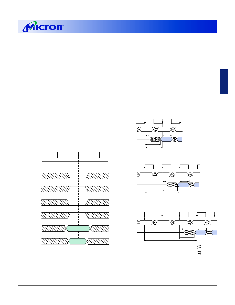
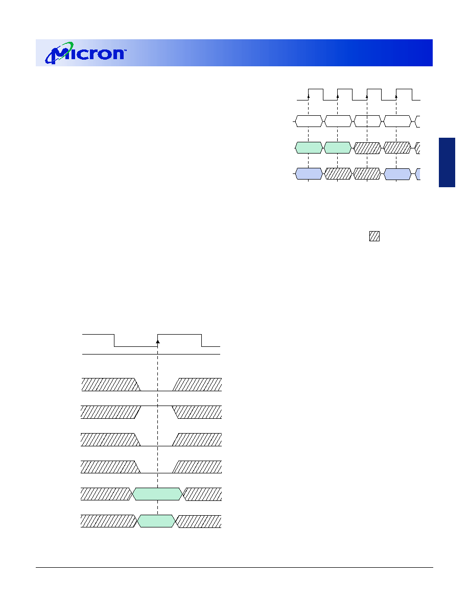
BANK/ROW ACTIVATION
Before any READ or WRITE commands can be is-
sued to a bank within the SyncFlash memory, a row in
that bank must be "opened." (Note: A row will not be
activated for LCR/active/read or LCR/active write com-
mand sequences, see the Flash Memory Architecture
section for additional information). This is accom-
plished via the ACTIVE command, which selects both
the bank and the row to be activated.
After opening a row (issuing an ACTIVE command),
a READ or WRITE command may be issued to that row,
subject to the
t
RCD specification.
t
RCD (MIN) should
be divided by the clock period and rounded up to the
next whole number to determine the earliest clock edge
after the ACTIVE command on which a READ or WRITE
command can be entered. For example, a
t
RCD specifi-
cation of 30ns with a 90 MHz clock (11.11ns period)
results in 2.7 clocks rounded to 3. This is reflected in
Figure 4, which covers any case where 2 <
t
RCD (MIN)/
t
CK
3 . (The same procedure is used to convert other
specification limits from time units to clock cycles).
A subsequent ACTIVE command to a different row
in the same bank can be issued without having to close
a previous active row, provided the minimum time in-
terval between successive ACTIVE commands to the
same bank is defined by
t
RC.
A subsequent ACTIVE command to another bank
can be issued while the first bank is being accessed,
which results in a reduction of total row access over-
head. The minimum time interval between successive
ACTIVE commands to different banks is defined by
t
RRD.
CS#
WE#
CAS#
RAS#
CKE
CLK
A0≠A10
ROW
ADDRESS
HIGH
BA0, BA1
BANK
ADDRESS
15
4 Meg x 16 SyncFlash
Micron Technology, Inc., reserves the right to change products or specifications without notice.
MT28S4M16LC_6.p65 ≠ Rev. 6, Pub. 9/01
©2001, Micron Technology, Inc.
4 MEG x 16
SYNCFLASH MEMORY
SDRAM
READs
READ bursts are initiated with a READ command,
as shown in Figure 5.
The starting column and bank addresses are pro-
vided with the READ command.
During READ bursts, the valid data-out element
from the starting column address will be available fol-
lowing the CAS latency after the READ command. Each
subsequent data-out element will be valid by the next
positive clock edge. Figure 6 shows general timing for
one, two, and three CAS latency settings.
Upon completion of a burst, assuming no other com-
mands have been initiated, the DQs will go High-Z. A
full-page burst will continue until terminated. (At the
end of the page, it will wrap to column 0 and continue.)
Data from any READ burst may be truncated with a
subsequent READ command, and data from a fixed-
length READ burst may be immediately followed by
data from a subsequent READ command. In either
case, a continuous flow of data can be maintained. The
first data element from the new burst follows either the
last element of a completed burst, or the last desired
data element of a longer burst that is being truncated.
Figure 5
READ Command
Figure 6
CAS Latency
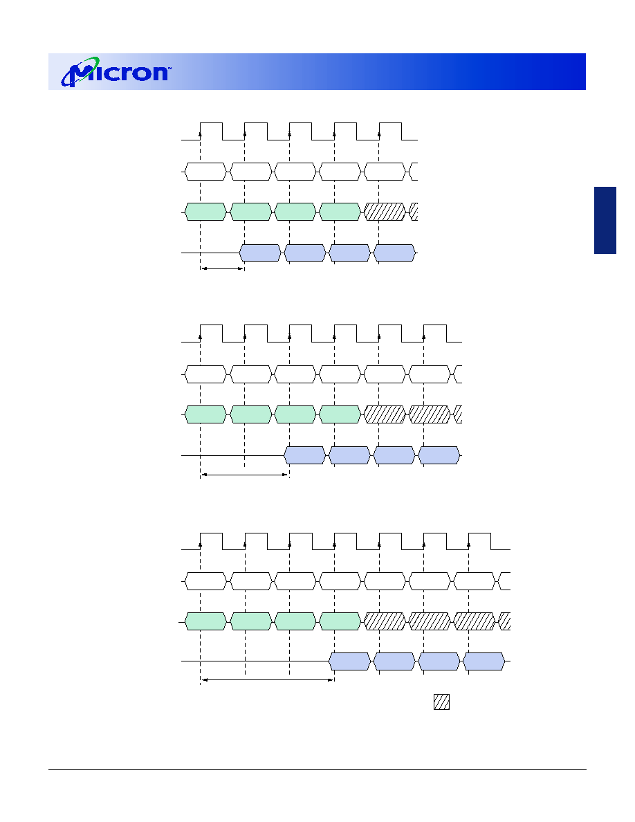
The new READ command should be issued x cycles
before the clock edge at which the last desired data
element is valid, where x equals the CAS latency minus
one. This is shown in Figure 7 for CAS latencies of one,
two, and three; data element n + 3 is either the last of a
burst of four, or the last desired of a longer burst. The
SyncFlash memory uses a pipelined architecture and
therefore does not require the 2n rule associated with a
prefetch architecture. A READ command can be initi-
ated on any clock cycle following a previous READ com-
mand. Full-speed, random read accesses within a page
can be performed as shown in Figure 8, or each subse-
quent READ may be performed to a different bank.
Data from any READ burst may be truncated with a
CS#
WE#
CAS#
RAS#
CKE
CLK
COLUMN
ADDRESS
A0≠A7
BA0, BA1
BANK
ADDRESS
HIGH
CLK
DQ
T2
T1
T3
T0
CAS Latency = 3
LZ
D
OUT
tOH
t
COMMAND
NOP
READ
tAC
NOP
T4
NOP
DON'T CARE
UNDEFINED
CLK
DQ
T2
T1
T0
CAS Latency = 1
LZ
D
OUT
tOH
t
COMMAND
NOP
READ
tAC
CLK
DQ
T2
T1
T3
T0
CAS Latency = 2
LZ
D
OUT
tOH
t
COMMAND
NOP
READ
tAC
NOP

16
4 Meg x 16 SyncFlash
Micron Technology, Inc., reserves the right to change products or specifications without notice.
MT28S4M16LC_6.p65 ≠ Rev. 6, Pub. 9/01
©2001, Micron Technology, Inc.
4 MEG x 16
SYNCFLASH MEMORY
SDRAM
Figure 7
Consecutive READ Bursts
CLK
DQ
D
OUT
n
T2
T1
T4
T3
T5
T0
COMMAND
ADDRESS
READ
NOP
NOP
NOP
BANK,
COL n
DON'T CARE
NOP
BANK,
COL b
D
OUT
n + 1
D
OUT
n + 2
D
OUT
n + 3
D
OUT
b
READ
X = 0 cycles
NOTE: Each READ command may be to either bank. DQM is LOW.
CAS Latency = 1
CLK
DQ
D
OUT
n
T2
T1
T4
T3
T6
T5
T0
COMMAND
ADDRESS
READ
NOP
NOP
NOP
NOP
BANK,
COL n
NOP
BANK,
COL b
D
OUT
n + 1
D
OUT
n + 2
D
OUT
n + 3
D
OUT
b
READ
X = 1 cycle
CAS Latency = 2
CLK
DQ
D
OUT
n
T2
T1
T4
T3
T6
T5
T0
COMMAND
ADDRESS
READ
NOP
NOP
NOP
NOP
BANK,
COL n
NOP
BANK,
COL b
D
OUT
n + 1
D
OUT
n + 2
D
OUT
n + 3
D
OUT
b
READ
NOP
T7
X = 2 cycles
CAS Latency = 3
17
4 Meg x 16 SyncFlash
Micron Technology, Inc., reserves the right to change products or specifications without notice.
MT28S4M16LC_6.p65 ≠ Rev. 6, Pub. 9/01
©2001, Micron Technology, Inc.
4 MEG x 16
SYNCFLASH MEMORY
SDRAM
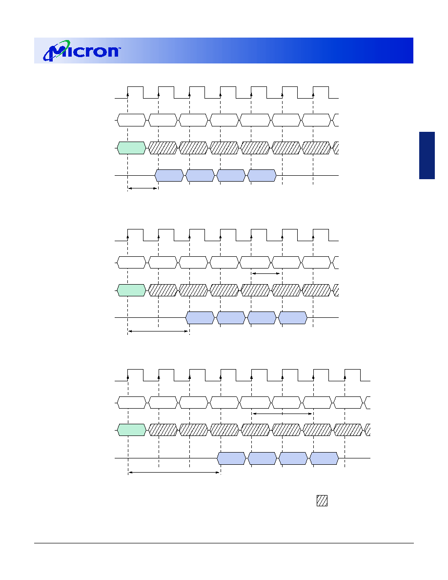
Figure 8
Random Read Accesses Within a Page
CLK
DQ
T2
T1
T4
T3
T6
T5
T0
COMMAND
ADDRESS
READ
NOP
NOP
BANK,
COL n
DON'T CARE
D
OUT
n
D
OUT
a
D
OUT
x
D
OUT
m
READ
NOTE: Each READ command may be to either bank. DQM is LOW.
READ
READ
NOP
BANK,
COL a
BANK,
COL x
BANK,
COL m
CLK
DQ
D
OUT
n
T2
T1
T4
T3
T5
T0
COMMAND
ADDRESS
READ
NOP
BANK,
COL n
D
OUT
a
D
OUT
x
D
OUT
m
READ
READ
READ
NOP
BANK,
COL a
BANK,
COL x
BANK,
COL m
CLK
DQ
D
OUT
n
T2
T1
T4
T3
T0
COMMAND
ADDRESS
READ
NOP
BANK,
COL n
D
OUT
a
D
OUT
x
D
OUT
m
READ
READ
READ
BANK,
COL a
BANK,
COL x
BANK,
COL m
CAS Latency = 1
CAS Latency = 2
CAS Latency = 3

18
4 Meg x 16 SyncFlash
Micron Technology, Inc., reserves the right to change products or specifications without notice.
MT28S4M16LC_6.p65 ≠ Rev. 6, Pub. 9/01
©2001, Micron Technology, Inc.
4 MEG x 16
SYNCFLASH MEMORY
SDRAM
Figure 9
READ to WRITE
subsequent WRITE command (WRITE commands
must be preceded by LCR/ACTIVE), and data from a
fixed-length READ burst may be immediately followed
by data from a subsequent WRITE command (subject
to bus turnaround limitations). The WRITE may be
initiated on the clock edge immediately following the
last (or last desired) data element from the READ burst,
provided that I/O contention can be avoided. In a given
system design, there may be the possibility that the
device driving the input data would go Low-Z before
the SyncFlash memory DQs go High-Z. In this case, at
least a single-cycle delay should occur between the last
read data and the WRITE command.
The DQM input is used to avoid I/O contention as
shown in Figure 9. The DQM signal must be asserted
(HIGH) at least two clocks prior to the WRITE command
(DQM latency is two clocks for output buffers) to sup-
press data-out from the READ. Once the WRITE com-
mand is registered, the DQs will go High-Z (or remain
High-Z) regardless of the state of the DQM signal. The
DQM signal must be de-asserted prior to the WRITE
command (DQM latency is zero clocks for input buff-
ers) to ensure that the written data is not masked. Fig-
ure 9 shows the case where the clock frequency allows
for bus contention to be avoided without adding a NOP
cycle.
A fixed-length or full-page READ burst can be trun-
cated with ACTIVE TERMINATE (may or may not be
bank specific) or BURST TERMINATE (not bank spe-
cific). The ACTIVE TERMINATE or BURST TERMINATE
command should be issued x cycles before the clock
edge at which the last desired data element is valid,
where x equals the CAS latency minus one. This is
shown in Figure 10 for each possible CAS latency; data
element n + 3 is the last desired data element of a burst
of four or the last desired of a longer burst.
READ
LCR
ACTIVE
WRITE
NOP
CLK
T2
T1
T4
T3
T0
DQM, H
DQ
D
OUT
n
COMMAND
D
IN
b
ADDRESS
BANK,
COL n
BANK,
COL b
DS
tHZ
t
tCK
NOTE:
A CAS latency of three is used for illustration. The
READ command may be to any bank, and the WRITE
command may be to any bank. If a CAS latency of one is
used, then DQM is not required.
DON'T CARE
40h
BANK
ROW
19
4 Meg x 16 SyncFlash
Micron Technology, Inc., reserves the right to change products or specifications without notice.
MT28S4M16LC_6.p65 ≠ Rev. 6, Pub. 9/01
©2001, Micron Technology, Inc.
4 MEG x 16
SYNCFLASH MEMORY
SDRAM
Figure 10
Terminating a READ Burst
CLK
DQ
D
OUT
n
T2
T1
T4
T3
T6
T5
T0
COMMAND
ADDRESS
READ
NOP
NOP
NOP
NOP
BANK,
COL n
NOP
D
OUT
n + 1
D
OUT
n + 2
D
OUT
n + 3
BURST
TERMINATE
NOP
T7
DON'T CARE
NOTE: DQM is LOW.
CLK
DQ
D
OUT
n
T2
T1
T4
T3
T6
T5
T0
COMMAND
ADDRESS
READ
NOP
NOP
NOP
BANK,
COL n
NOP
D
OUT
n + 1
D
OUT
n + 2
D
OUT
n + 3
BURST
TERMINATE
NOP
CLK
DQ
D
OUT
n
T2
T1
T4
T3
T6
T5
T0
COMMAND
ADDRESS
READ
NOP
NOP
NOP
BANK,
COL n
NOP
D
OUT
n + 1
D
OUT
n + 2
D
OUT
n + 3
BURST
TERMINATE
NOP
X = 0 cycles
CAS Latency = 1
X = 1 cycle
CAS Latency = 2
CAS Latency = 3
X = 2 cycles
20
4 Meg x 16 SyncFlash
Micron Technology, Inc., reserves the right to change products or specifications without notice.
MT28S4M16LC_6.p65 ≠ Rev. 6, Pub. 9/01
©2001, Micron Technology, Inc.
4 MEG x 16
SYNCFLASH MEMORY
SDRAM
WRITEs
A single-location WRITE is initiated with a WRITE
command (preceded by LCR/ACTIVE, see Truth Table
2), as shown in Figure 11. The starting column and
bank addresses are provided with the WRITE com-
mand. Once a WRITE command is registered, a READ
command can be executed as defined by Truth Tables
4 and 5. An example is shown in Figure 12.
During a WRITE, the valid data-in element will be
registered coincident with the WRITE command. Addi-
tional details on write sequence operations are found
in the Command Execution section.
ACTIVE TERMINATE
The ACTIVE TERMINATE command is functionally
equivalent to the SDRAM PRECHARGE command. Un-
like SDRAM, SyncFlash does not require a PRECHARGE
command to deactivate the open row in a particular
bank or the open rows in all banks. Asserting input A10
HIGH during an ACTIVE TERMINATE command will
terminate a BURST READ in any bank. When A10 is
LOW during an ACTIVE TERMINATE command, BA0
and BA1 will determine which bank will undergo a ter-
minate operation. ACTIVE TERMINATE is considered
a NOP for banks not addresssed by A10, BA0, BA1.
Figure 12
WRITE to READ
BURST READ/SINGLE WRITE
The burst read/single write mode is the default
mode for the MT28S4M16LC; the write burst mode bit
(M9) in the mode register is set to a logic 1. All WRITE
commands result in the access of a single column loca-
tion (burst of one). READ commands access columns
according to the programmed burst length and se-
quence.
POWER-DOWN
Power-down occurs if CKE is registered LOW coinci-
dent with a NOP or COMMAND INHIBIT, when no
accesses are in progress. Entering power-down deacti-
vates the input and output buffers (excluding CKE)
after ISM operations (including WRITE operations) are
completed, for power savings while in standby.
The power-down state is exited by registering a NOP
or COMMAND INHIBIT and CKE HIGH at the desired
clock edge (meeting
t
CKS).
See the Reset/Deep Power-Down description in the
Flash Memory Functional Description for maximum
power savings mode.
CLOCK SUSPEND
The clock suspend mode occurs when a column ac-
cess/burst is in progress and CKE is registered LOW. In
the clock suspend mode, the internal clock is deacti-
vated, "freezing" the synchronous logic.
Figure 11
WRITE Command
CS#
WE#
CAS#
RAS#
CKE
CLK
COLUMN
ADDRESS
A0≠A7
BA0, BA1
BANK
ADDRESS
HIGH
CLK
DQ
T2
T1
T3
T0
COMMAND
ADDRESS
READ
DON'T CARE
WRITE
BANK,
COL n
D
IN
n
NOP
NOP
BANK,
COL b
NOTE:
A CAS latency of two is used for illustration.
The WRITE command may be to any bank and the
READ command may be to any bank. DQM is
LOW. For more details, refer to Truth Tables 4
and 5.
Db
OUT

21
4 Meg x 16 SyncFlash
Micron Technology, Inc., reserves the right to change products or specifications without notice.
MT28S4M16LC_6.p65 ≠ Rev. 6, Pub. 9/01
©2001, Micron Technology, Inc.
4 MEG x 16
SYNCFLASH MEMORY
SDRAM
Figure 14
Clock Suspend During READ Burst
TRUTH TABLE 3 ≠ CKE
(Notes: 1-4)
CKE
n-1
CKE
n
CURRENT STATE
COMMAND
n
ACTION
n
NOTES
L
L
Clock Standby
X
Maintain Clock Standby
Clock Suspend
X
Maintain Clock Suspend
L
H
Clock Standby
COMMAND INHIBIT or NOP
Exit Clock Standby
5
Clock Suspend
X
Exit Clock Suspend
6
H
L
No Burst in Progress
COMMAND INHIBIT or NOP
Clock Standby
Reading
VALID
Clock Suspend
H
H
See Truth Table 4
NOTE: 1. "CKE
n
" is the logic state of CKE at clock edge n; "CKE
n-1
" was the state of CKE at the previous clock edge.
2. "Current State" is the state of the SyncFlash memory immediately prior to clock edge n.
3. "Command
n
" is the command registered at clock edge n and "Action
n
" is a result of Command
n
.
4. All states and sequences not shown are illegal or reserved.
5. Exiting POWER-DOWN at clock edge n will put the device in the idle state in time for clock edge n + 1 (provided that
t
CKS is met).
6. After exiting CLOCK SUSPEND at clock edge n, the device will resume operation and recognize the next command at
clock edge n + 1.
tRAS
tRCD
tRC
All banks idle
Input buffers gated off
Exit power-down mode.
(
)
(
)
(
)
(
)
(
)
(
)
tCKS
t CKS
COMMAND
NOP
ACTIVE
Enter power-down mode.
NOP
CLK
CKE
(
)
(
)
(
)
(
)
Coming out of a power-down sequence (active),
t
CKS (CKE setup time) must be greater than or equal to 3ns.
Figure 13
Power-Down
DON'T CARE
CLK
DQ
D
OUT
n
T2
T1
T4
T3
T6
T5
T0
COMMAND
ADDRESS
READ
NOP
NOP
NOP
BANK,
COL n
NOP
D
OUT
n + 1
D
OUT
n + 2
D
OUT
n + 3
NOTE: For this example, CAS latency = 2, burst length = 4 or greater, and
DM is LOW.
CKE
INTERNAL
CLOCK
NOP
For each positive clock edge on which CKE is
sampled LOW, the next internal positive clock edge is
suspended. Any command or data present on the in-
put pins at the time of a suspended internal clock edge
is ignored, any data present on the DQ pins remains
driven, and burst counters are not incremented, as
long as the clock is suspended (see example in Figure
14).
Clock suspend mode is exited by registering CKE
HIGH; the internal clock and related operation will re-
sume on the subsequent positive clock edge.

22
4 Meg x 16 SyncFlash
Micron Technology, Inc., reserves the right to change products or specifications without notice.
MT28S4M16LC_6.p65 ≠ Rev. 6, Pub. 9/01
©2001, Micron Technology, Inc.
4 MEG x 16
SYNCFLASH MEMORY
SDRAM
TRUTH TABLE 4 ≠ CURRENT STATE BANK n; COMMAND TO BANK n
(Notes: 1-6)
CURRENT STATE CS# RAS# CAS# WE#
COMMAND/ACTION
NOTES
Any
H
X
X
X
COMMAND INHIBIT (NOP/continue previous operation)
L
H
H
H
NO OPERATION (NOP/continue previous operation)
L
L
H
H
ACTIVE (Select and activate row)
Idle
L
L
L
H
LOAD COMMAND REGISTER
L
L
L
L
LOAD MODE REGISTER
7
L
L
H
L
ACTIVE TERMINATE
8
L
H
L
H
READ (Select column and start READ burst)
Row Active
L
H
L
L
WRITE (Select column and start WRITE)
L
L
H
L
ACTIVE TERMINATE
8
L
L
L
H
LOAD COMMAND REGISTER
L
H
L
H
READ (Select column and start new READ burst)
Read
L
L
H
L
ACTIVE TERMINATE
8
L
H
H
L
BURST TERMINATE
9
L
L
L
H
LOAD COMMAND REGISTER
Write
L
H
L
H
READ (Select column and start new READ burst)
10
L
L
L
H
LOAD COMMAND REGISTER
NOTE: 1. This table applies when CKE
n-1
was HIGH and CKE
n
is HIGH (see Truth Table 3).
2. This table is bank specific, except where noted; i.e., the current state is for a specific bank and the commands shown
are those allowed to be issued to that bank, when in that state. Exceptions are covered in the notes below.
3. Current state definitions:
Idle: The bank is not in read or write mode.
Row Active: A row in the bank has been activated and
t
RCD has been met. No data bursts/accesses and no
register accesses are in progress.
Read: A READ burst has been initiated and has not yet terminated or been terminated.
Write: A WRITE operation has been initiated to the SyncFlash ISM and has not yet completed.
4. The following states must not be interrupted by a command issued to the same bank. COMMAND INHIBIT or NOP
commands, or allowable commands to the other bank should be issued on any clock edge occurring during these states.
Allowable commands to the other bank are determined by its current state and Truth Table 4, and according to Truth
Table 5.
Active Terminate: Starts with registration of an ACTIVE TERMINATE command and ends on the next clock cycle. The
bank will then be in the idle state.
Row Activating: Starts with registration of an ACTIVE command and ends when
t
RCD is met. Once
t
RCD is met, the
bank will be in the row active state.
5. The following states must not be interrupted by any executable command; COMMAND INHIBIT or NOP commands must
be applied on each positive clock edge during these states.
Accessing Mode
Register: Starts with registration of a LOAD MODE REGISTER command and ends when
t
MRD
has been met. Once
t
MRD is met, the SyncFlash memory will be in the all banks idle state.
Initialize Mode: Starts with RP# transitioning from LOW to HIGH and ends after 100µs delay.
6. All states and sequences not shown are illegal or reserved.
7. Not bank specific; requires that all banks are idle.
8. May or may not be bank specific.
9. Not bank specific; BURST TERMINATE affects the most recent READ burst, regardless of bank.
10. A READ operation to the bank under ISM control will output the contents of the row activated prior to the LCR/active/
write sequence (see Truth Table 2).
23
4 Meg x 16 SyncFlash
Micron Technology, Inc., reserves the right to change products or specifications without notice.
MT28S4M16LC_6.p65 ≠ Rev. 6, Pub. 9/01
©2001, Micron Technology, Inc.
4 MEG x 16
SYNCFLASH MEMORY
SDRAM
TRUTH TABLE 5 ≠ CURRENT STATE BANK n; COMMAND TO BANK m
(Notes: 1-6)
CURRENT STATE CS# RAS# CAS# WE#
COMMAND/ACTION
NOTES
Any
H
X
X
X
COMMAND INHIBIT (NOP/continue previous operation)
L
H
H
H
NO OPERATION (NOP/continue previous operation)
Idle
X
X
X
X
Any Command Otherwise Allowed to Bank m
L
L
H
H
ACTIVE (Select and activate row)
Row Activating,
L
H
L
H
READ (Select column and start READ burst)
Active, or
L
H
L
L
WRITE (Select column and start WRITE)
Active
L
L
H
L
ACTIVE TERMINATE
Terminate
L
L
L
H
LOAD COMMAND REGISTER
L
L
H
H
ACTIVE (Select and activate row)
Read
L
H
L
H
READ (Select column and start new READ burst)
L
L
H
L
ACTIVE TERMINATE
L
L
L
H
LOAD COMMAND REGISTER
L
L
H
H
ACTIVE (Select and activate row)
L
H
L
H
READ (Select column and start READ burst)
Write
L
L
H
L
ACTIVE TERMINATE
L
H
H
L
BURST TERMINATE
L
L
L
H
LOAD COMMAND REGISTER
NOTE: 1. This table applies when CKE
n-1
was HIGH and CKE
n
is HIGH (see Truth Table 3).
2. This table describes alternate bank operation, except where noted; i.e., the current state is for bank n and the
commands shown are those allowed to be issued to bank m (assuming that bank m is in such a state that the given
command is allowable). Exceptions are covered in the notes below.
3. Current state definitions:
Idle: The bank is not in initialize, read, write mode.
Row Active: A row in the bank has been activated and
t
RCD has been met. No data bursts/accesses and no
register accesses are in progress.
Read: A READ burst has been initiated and has not yet terminated or been terminated.
Write: A WRITE operation has been initiated to the SyncFlash ISM and has not yet completed.
4. LOAD MODE REGISTER command may only be issued when all banks are idle.
5. A BURST TERMINATE command cannot be issued to another bank; it applies to the bank represented by the current state
only.
6. All states and sequences not shown are illegal or reserved.

FLASH
24
4 Meg x 16 SyncFlash
Micron Technology, Inc., reserves the right to change products or specifications without notice.
MT28S4M16LC_6.p65 ≠ Rev. 6, Pub. 9/01
©2001, Micron Technology, Inc.
4 MEG x 16
SYNCFLASH MEMORY
FLASH MEMORY
FUNCTIONAL DESCRIPTION
The SyncFlash memory incorporates a number of
features that make it ideally suited for code storage
and execute-in-place applications on an SDRAM bus.
The memory array is segmented into individual erase
blocks. Each block may be erased without affecting
data stored in other blocks. These memory blocks are
read, programmed, and erased by issuing commands
to the command execution logic (CEL). The CEL con-
trols the operation of the internal state machine (ISM),
which completely controls all ERASE NVMODE REGIS-
TER, PROGRAM NVMODE REGISTER, PROGRAM,
BLOCK ERASE, BLOCK PROTECT, DEVICE PROTECT,
UNPROTECT ALL BLOCKS, and VERIFY operations.
The ISM protects each memory location from
overerasure and optimizes each memory location for
maximum data retention. In addition, the ISM greatly
simplifies the control necessary for programming the
device in-system or in an external programmer.
The Flash Memory Functional Description provides
detailed information on the operation of the SyncFlash
memory and is organized into these sections:
∑
Command Interface
∑
Memory Architecture
∑
Output (READ) Operations
∑
Input Operations
∑
Command Execution
∑
RESET/Power-Down Mode
∑
Error Handling
∑
PROGRAM/ERASE Cycle Endurance
COMMAND INTERFACE
All Flash operations are executed with LCR (LOAD
COMMAND REGISTER), LCR/ACTIVE/READ, or LCR/
ACTIVE/WRITE commands and command sequences
as defined in Truth Tables 1 and 2. See the SDRAM
Interface Functional Description for information on
reading the memory array.
Address pins A0≠A7 are used to input 8-bit com-
mands during the LCR command cycle. This command
will identify which flash operation is initiated.
Certain LCR/active/write command sequences re-
quire an 8-bit confirmation code on the WRITE cycle.
The confirmation code is input on DQ0≠DQ7.
All input commands are latched on the positive clock
edge.
MEMORY ARCHITECTURE
The 64Mb SyncFlash is a four-bank architecture with
four erasable "blocks" per bank. By erasing blocks
rather than the entire array, the total device endur-
ance is enhanced, as is system flexibility. Only the
ERASE and BLOCK PROTECT functions are block ori-
ented. The four banks have simultaneous read-while-
write functionality. An ISM PROGRAM or ERASE opera-
tion to any bank can occur simultaneously with a READ
to any other bank.
The SyncFlash memory has a single background
operation ISM to control power-up initialization,
ERASE, PROGRAM, and PROTECT operations. ISM
operations are initiated with an LCR/ACTIVE/WRITE
command sequence. Only one ISM operation can occur
at any time; however, certain other commands, includ-
ing READ operations, can be performed while an ISM
operation is taking place. A new LCR/active/write com-
mand sequence will not be permitted until the current
ISM operation is complete. An operational command
controlled by the ISM is defined as either a bank-level
operation or a device-level operation.
PROGRAM and ERASE are bank-level ISM opera-
tions. After an ISM bank-level operation has been initi-
ated, a READ may be issued to any bank; however, a
READ to the bank under ISM control will output the
contents of the row activated prior to the LCR/active/
write command sequence.
ERASE NVMODE REGISTER, PROGRAM NVMODE
REGISTER, BLOCK PROTECT, DEVICE PROTECT, and
UNPROTECT ALL BLOCKS are device-level ISM opera-
tions. Once an ISM device-level operation has been
initiated, a READ to any bank will output the contents
of the array.
A read status register command sequence may be
issued to determine completion of the ISM operation.
When SR7 = 1, the ISM operation is complete and a new
ISM operation may be initiated.
PROTECTED BLOCKS
The 64Mb SyncFlash memory is organized into 16
erasable memory blocks. Each block may be software
protected by issuing the appropriate LCR/active/write
sequence for a BLOCK PROTECT operation.
The blocks at locations 0 and 15 have additional
protection to prevent inadvertent PROGRAM or ERASE
operations in 3.3V-only platforms. Once a PROTECT
BLOCK operation has been executed to these blocks,
an UNPROTECT ALL BLOCKS operation will unlock all
blocks except the blocks at locations 0 and 15 unless
RP# = V
HH
. This provides additional security for critical
code during in-system firmware updates should an
unintentional power disruption or system reset occur.

FLASH
25
4 Meg x 16 SyncFlash
Micron Technology, Inc., reserves the right to change products or specifications without notice.
MT28S4M16LC_6.p65 ≠ Rev. 6, Pub. 9/01
©2001, Micron Technology, Inc.
4 MEG x 16
SYNCFLASH MEMORY
A second level of block protection is possible
by completing a hardware DEVICE PROTECT opera-
tion. DEVICE PROTECT prevents block protect bit
modification.
The protection status of any block may be checked
by reading the protect bits with a read device configu-
ration command sequence.
COMMAND EXECUTION LOGIC (CEL)
SyncFlash operations are executed by issuing the
appropriate commands to the CEL. The CEL receives
and interprets commands to the device. These com-
mands control the operation of the ISM and the read
path (i.e., memory array, device configuration, or sta-
tus register). Commands may be issued to the CEL
while the ISM is active. However, there are restrictions
on what commands are allowed in this condition. See
the Command Execution section for more details.
INTERNAL STATE MACHINE (ISM)
Power-up initialization, erase, program, and pro-
tect timings are simplified by using an ISM to control all
programming algorithms in the memory array. The ISM
ensures protection against overerasure and optimizes
programming margin to each cell.
During PROGRAM operations, the ISM automati-
cally increments and monitors PROGRAM attempts,
verifies programming margin on each memory cell, and
updates the ISM status register. When BLOCK ERASE is
performed, the ISM automatically overwrites the en-
tire addressed block (eliminates overerasure), incre-
ments and monitors ERASE attempts, and sets bits in
the ISM status register.
ISM STATUS REGISTER
The 16-bit ISM status register allows an external
processor to monitor the status of the ISM during de-
vice initialization, ERASE NVMODE REGISTER, PRO-
GRAM NVMODE REGISTER, PROGRAM, ERASE,
BLOCK PROTECT, DEVICE PROTECT or UNPROTECT
ALL BLOCKS, and any related errors. ISM operations
and related errors can be monitored by reading status
register bits on DQ0≠DQ8.
All of the defined bits are set by the ISM, but only
the ISM status bits (SR0, SR1, SR2, SR7) are cleared by
the ISM. The erase/unprotect block, program/protect
block, and device protection bits must be cleared by
the host system using the CLEAR STATUS REGISTER
command. This allows the user to choose when to poll
and clear the status register. For example, the host
system may perform multiple PROGRAM operations
before checking the status register instead of checking
after each individual PROGRAM.
A V
CC
power sequence error is cleared by re-
initializing the device.
Asserting the RP# signal or powering down the de-
vice will also clear the status register.
Figure 15
Memory Address Map
256K-Word Block
256K-Word Block
256K-Word Block
256K-Word Block
256K-Word Block
256K-Word Block
256K-Word Block
256K-Word Block
256K-Word Block
256K-Word Block
256K-Word Block
256K-Word Block
256K-Word Block
256K-Word Block
256K-Word Block
256K-Word Block
Bank 0
15
14
13
12
11
10
9
8
7
6
5
4
3
2
1
0
3 FFF FFh
3
3 BFF FFh
3
3 7FF FFh
3
3 3FF FFh
3 000 00h
2
FFh
FFF
C00
2
00h
BFF
2
FFh
2 800 00h
7FF
2
FFh
400
2
00h
3FF
2
FFh
000
2
00h
FFF
1
FFh
C00 00h
1
BFF
1
FFh
800 00h
1
7FF FFh
1
400 00h
1
1
FFh
3FF
000 00h
1
FFh
FFF
0
C00
0
00h
0
FFh
BFF
0
00h
800
0
FFh
7FF
0
00h
400
0
FFh
3FF
0
00h
000
Bank 1
Bank 2
Bank 3
Unlock Blocks
(RP# = V
HH
)
Word-Wide (x16)
Unlock Blocks
(RP# = V
IH
)
Bank
Column
Row
00h
C00
800 00h
400 00h
ADDRESS RANGE
NOTE: See Block Lock and Unlock Flowchart Sequences for
additional information

FLASH
26
4 Meg x 16 SyncFlash
Micron Technology, Inc., reserves the right to change products or specifications without notice.
MT28S4M16LC_6.p65 ≠ Rev. 6, Pub. 9/01
©2001, Micron Technology, Inc.
4 MEG x 16
SYNCFLASH MEMORY
OUTPUT (READ) OPERATIONS
SyncFlash memory features three different types of
READs. Depending on the mode, a READ operation
will produce data from the memory array, status regis-
ter, or one of the device configuration registers.
SyncFlash memory is in the array read mode unless a
status register or device register read is initiated or in
progress.
A READ to the device configuration register or the
status register must be preceded by LCR/ACTIVE. The
burst length of data-out is defined by the mode regis-
ter settings. Reading the device configuration register
or status register will not disrupt data in a previously
opened (or "activated") page. When the burst is com-
plete, a subsequent READ will read the array. How-
ever, several differences exist and are described in the
following section. Moving between modes to perform a
specific READ will be covered in the Command Execu-
tion section.
MEMORY ARRAY
A READ command to any bank will output the con-
tents of the memory array. While a PROGRAM or ERASE
ISM operation is in progress, a READ to any location in
the bank under ISM control will output the contents of
the row activated prior to the LCR/active/write com-
mand sequence; a READ to any other bank will output
the contents of the array. All commands and their op-
erations are covered in the SDRAM Interface Functional
Description section.
STATUS REGISTER
Reading the status register requires an LCR/active/
read command sequence. The status register contents
are latched on the next positive clock edge subject to
CAS latencies. The burst length of the status register
data-out is defined by the mode register.
All commands and their operations are covered in
the Command Execution section.
DEVICE CONFIGURATION REGISTERS
Reading the device ID, manufacturer compatibility
ID, device protection status, and block protect status
requires the same input sequencing as when reading
the status register except that specific addresses must
be issued.
All commands and their operations are covered in
the Command Execution section.
INPUT OPERATIONS
An LCR/active/write command sequence is re-
quired to program the array, or to perform an ERASE,
PROTECT, or UNPROTECT operation. The first cycle of
an input operation is LCR where inputs A0≠A7 deter-
mine the input command being executed to the CEL.
An input operation will not disrupt data in a previously
opened page.
The DQ pins are used either to input data to the
array or to input a command to the command execu-
tion logic (CEL) during the WRITE cycle.
More information describing how to program, erase,
protect, or unprotect the device is provided in the Com-
mand Execution section.
MEMORY ARRAY
Programming or erasing the memory array sets the
desired bits to logic 0s but cannot change a given bit to
a logic 1 from a logic 0. Setting any bit to a logic 1 re-
quires that the entire block be erased. Programming a
protected block requires that the RP# pin be brought to
V
HH
. A0≠A11 provide the address to be programmed,
while the data to be programmed in the array is input
on the DQ pins. The data and addresses are latched on
the rising edge of the clock. Details on how to input
data to the array is covered in the Command Execution
section.
COMMAND EXECUTION
Commands are issued to bring the device into dif-
ferent operational modes. Each mode has specific op-
erations that can be performed while in that mode. All
modes require that an LCR/active/read or LCR/active/
write sequence be issued, except CLEAR STATUS REG-
ISTER which is a single LCR command. Inputs A0≠A7
during the LCR command determine the command
being executed. The following section describes the
properties of each mode, and Truth Tables 1 and 2 list
all commands and command sequences required to
perform the desired operation. Read-while-write func-
tionality allows a background operation program or
erase to any bank while simultanously reading any
other bank.
The LCR/active/write command sequences in Truth
Table 2 must be completed on consecutive clock cycles.
However, in order to reduce bus contention issues, an
unlimited number of NOPs or COMMAND INHIBITs
can be issued throughout the LCR/active/write com-
mand sequence. For additional protection, these com-
mand sequences must have the same bank address for
the three command cycles.
If the bank address changes during the LCR/ac-
tive/write command sequence or if the command se-
quences are not consecutive (other than NOPs and
COMMAND INHIBITs), the program and erase status
bits (SR4 and SR5) will be set and the desired operation
will be aborted.

FLASH
27
4 Meg x 16 SyncFlash
Micron Technology, Inc., reserves the right to change products or specifications without notice.
MT28S4M16LC_6.p65 ≠ Rev. 6, Pub. 9/01
©2001, Micron Technology, Inc.
4 MEG x 16
SYNCFLASH MEMORY
STATUS REGISTER
Reading the status register requires an LCR/active/
read command sequence. The status register contents
are latched on the next positive clock edge subject to
CAS latencies for a burst length defined by the mode
register.
DEVICE CONFIGURATION
To read the device ID, manufacturer compatibility
ID, device protect bit, and each of the block protect
bits, the appropriate LCR/active/read command se-
quence for READ DEVICE CONFIGURATION must be
issued. Specific configuration addresses must be is-
sued to read the desired information. The manufac-
turer compatibility ID is read at 000h; the device ID is
read at 001h. The manufacturer compatibility ID and
device ID are output on DQ0≠DQ7. The device protect
bit is read at 003h; and each of the block protect bits is
read on the third address location within each block
(x02h). The device and block protect bits are output on
DQ0.
The device configuration register contents are out-
put subject to CAS latencies for a burst length defined
by the mode register.
PROGRAM SEQUENCE
Three commands on consecutive clock edges are
required to input data to the array (NOPs and COM-
MAND INHIBITS are permitted between cycles). In
the first cycle, LOAD COMMAND REGISTER is issued
with PROGRAM SETUP (40h) on A0≠A7, and the bank
address is issued on BA0, BA1. The next command is
ACTIVE, which identifies the row address and con-
firms the bank address. The third cycle is WRITE, dur-
ing which the column address, the bank address, and
data are issued. The ISM status bit will be set on the
following clock edge (subject to CAS latencies).
While the ISM is programming the array, the ISM
status bit (SR7) will be at "0." When the ISM status bit
(SR7) is set to a logic 1, programming is complete, and
the bank will be in the array read mode and ready for a
new ISM operation.
Programming hardware-protected blocks requires
that the RP# pin be set to V
HH
prior to the third cycle
(WRITE), and RP# must be held at V
HH
until the ISM
PROGRAM operation is complete. The program and
erase status bits (SR4 and SR5) will be set and the op-
eration aborted if the LCR/active/write command se-
quence is not completed on consecutive cycles or the
bank address changes for any of the three cycles. After
the ISM has initiated programming, it cannot be
aborted except by a RESET or by powering down the
device. Doing either while programming the array will
corrupt the data being written.
ERASE SEQUENCE
Executing an erase sequence will set all bits within a
block to logic 1. The command sequence necessary to
execute an ERASE is similar to that of a PROGRAM. To
provide added security against accidental block era-
sure, three consecutive command sequences on con-
secutive clock edges are required to initiate an ERASE
of a block. In the first cycle, LOAD COMMAND REGIS-
TER is issued with ERASE SETUP (20h) on A0≠A7, and
the bank address of the block to be erased is issued on
BA0, BA1. The next command is ACTIVE, where A10,
A11, BA0, and BA1 provide the address of the block to
be erased. The third cycle is WRITE, during which
ERASE CONFRIM (D0h) is issued on DQ0≠DQ7 and the
bank address is reissued. The ISM status bit will be set
on the following clock edge (subject to CAS latencies).
After ERASE CONFIRM (D0h) is issued, the ISM will
start erasing the addressed block. When the ERASE
operation is complete, the bank will be in the array read
mode and ready for an executable command. Erasing
hardware-protected blocks also requires that the RP#
pin be set to V
HH
prior to the third cycle (WRITE), and
RP# must be held at V
HH
until the erase operation is
complete (SR7 = 1). If the LCR/active/write command
sequence is not completed on consecutive cycles (NOPs
and COMMAND INHIBITs are permitted between
cycles), or the bank address changes for one or more of
the command cycles, the program and erase status bits
(SR4 and SR5) will be set.
PROGRAM AND ERASE NVMODE REGISTER
The contents of the mode register may be copied
into the nvmode register with a PROGRAM NVMODE
REGISTER command. Prior to programming the
nvmode register, an erase nvmode register command
sequence must be completed to set all bits in the
nvmode register to logic 1. The command sequence
necessary to execute an ERASE NVMODE REGISTER
and PROGRAM NVMODE REGISTER is similar to that
of a PROGRAM. See Truth Table 2 for more information
on the LCR/ACTIVE/WRITE commands necessary to
complete ERASE NVMODE REGISTER and PROGRAM
NVMODE REGISTER.
BLOCK PROTECT/UNPROTECT SEQUENCE
Executing a block protect sequence will enable the
first level of software/hardware protection for a given
block. The command sequence necessary to execute a
BLOCK PROTECT is similar to that of a PROGRAM. To
provide added security against accidental block pro-
tection, three consecutive command cycles are re-
quired to initiate a BLOCK PROTECT. In the first cycle,
LOAD COMMAND REGISTER is issued with PROTECT
SETUP (60h) on A0≠A7, and the bank address of the

FLASH
28
4 Meg x 16 SyncFlash
Micron Technology, Inc., reserves the right to change products or specifications without notice.
MT28S4M16LC_6.p65 ≠ Rev. 6, Pub. 9/01
©2001, Micron Technology, Inc.
4 MEG x 16
SYNCFLASH MEMORY
block to be protected is issued on BA0, BA1. The next
command is ACTIVE, which identifies a row in the block
to be protected and confirms the bank address. The
third cycle is WRITE, during which BLOCK PROTECT
CONFIRM (01h) is issued on DQ0≠DQ7, and the bank
address is reissued. The ISM status bit will be set on the
following clock edge (subject to CAS latencies) indicat-
ing the PROTECT operation is in progress.
If the LCR/ACTIVE/WRITE is not completed on con-
secutive cycles (NOPs and COMMAND INHIBITs are
permitted between cycles), or the bank address
changes, the write and erase status bits (SR4 and SR5)
will be set and the operation will be aborted. When the
ISM status bit (SR7) is set to a logic 1, the PROTECT
opertation is complete.
Once a block protect bit has been set to a "1" (pro-
tected), it can only be reset to a "0" if the UNPROTECT
ALL BLOCKS command is executed. The unprotect all
blocks command sequence is similar to the block pro-
tect sequence; however, in the third cycle, a WRITE is
issued with UNPROTECT ALL BLOCKS CONFIRM (D0h)
and addresses are "Don't Care." For additional infor-
mation, refer to Truth Table 2.
The blocks at locations 0 and 15 have additional
security. Once the block protect bits at locations 0 and
15 have been set to a "1" (protected), each bit can only
be reset to a "0" if RP# is brought to V
HH
prior to the third
cycle (WRITE) of the UNPROTECT operation, and held
at V
HH
until the operation is complete (SR7 = 1).
If the device protect bit is set, RP# must be brought
to V
HH
prior to the third cycle and held at V
HH
until the
BLOCK PROTECT or UNPROTECT ALL BLOCKS opera-
tion is complete.
To check a block's protect status, a read device con-
figuration command sequence may be issued.
DEVICE PROTECT SEQUENCE
Executing a device protect sequence will set the
device protect bit to a "1" and prevent block protect bit
modification. The command sequence necessary to
execute a DEVICE PROTECT is similar to that of a PRO-
GRAM. Three consecutive command cycles are re-
quired to initiate a DEVICE PROTECT. In the first cycle,
LOAD COMMAND REGISTER is issued with PROTECT
SETUP (60h) on A0≠A7, and a bank address is issued on
BA0, BA1. The bank address is "Don't Care," but the
same bank address must be used for all three cycles.
The next command is ACTIVE. The third cycle is WRITE,
during which DEVICE PROTECT (F1h) is issued on
DQ0≠DQ7. RP# must be brought to V
HH
prior to regis-
tration of the WRITE command. The ISM status bit will
be set on the following clock edge (subject to CAS laten-
cies). RP# must be held at V
HH
until the PROTECT op-
eration is complete (SR7 = 1).
Once the device protect bit is set, it can only be reset
to a "0" by issuing a BLOCK UNPROTECT command
with RP# at V
HH
during the operation. With the device
protect bit set to a "1," BLOCK PROTECT or BLOCK
UNPROTECT is prevented unless RP# is at V
HH
during
either operation. The device protect bit does not affect
PROGRAM or ERASE operations.
RESET/DEEP POWER-DOWN MODE
To allow for maximum power conservation, the de-
vice features a very low current, deep power-down
mode.
To enter this mode, the RP# pin (reset/power-down)
is taken to V
SS
±0.2V. To prevent an inadvertent RESET,
RP# must be held at V
SS
for 50ns prior to the device
entering the reset mode. With RP# held at V
SS
, the de-
vice will enter the deep power-down mode. After the
device enters the deep power-down mode, a transition
from LOW to HIGH on RP# will result in a device power-
up initialization sequence as outlined in the Device
Initialization section. Transitioning RP# from LOW to
HIGH after entering the reset mode but prior to enter-
ing deep power-down mode (i.e., less than 100ns) will
require a 1µs delay prior to issuing an executable com-
mand.
When the device enters the deep power-down
mode, all buffers excluding the RP# buffer are disabled
and the current draw is a maximum of 100µA at 3.6V
V
CC
. The input to RP# must remain at V
SS
during deep
power-down. Entering the RESET mode clears the Sta-
tus Register.
ERROR HANDLING
After the ISM status bit (SR7) has been set, the de-
vice protect (SR3), write/protect block (SR4) and erase/
unprotect (SR5) status bits may be checked. If one or a
combination of SR3, SR4, SR5 status bits has been set,
an error has occurred. SR8 is set when an inadvertent
power failure occurs during device initialization. The
device should be reinitialized to ensure proper device
operation. The ISM cannot reset SR3, SR4, SR5 or SR8.
To clear these bits, CLEAR STATUS REGISTER (50h)
must be given. Table 5 lists the combination of errors.
PROGRAM/ERASE CYCLE ENDURANCE
SyncFlash memory is designed and fabricated to
meet advanced code and data storage requirements.
Operation outside specification limits may reduce the
number of PROGRAM and ERASE cycles that may be
performed on the device. Each block is designed and
processed for a minimum of 100,000-PROGRAM/
ERASE-cycle endurance.

FLASH
29
4 Meg x 16 SyncFlash
Micron Technology, Inc., reserves the right to change products or specifications without notice.
MT28S4M16LC_6.p65 ≠ Rev. 6, Pub. 9/01
©2001, Micron Technology, Inc.
4 MEG x 16
SYNCFLASH MEMORY
STATUS
BIT #
STATUS REGISTER BIT
DESCRIPTION
SR15-
RESERVED
Reserved for future use.
SR9
SR8
V
CC
POWER SEQUENCE STATUS (VPS)
VPS is set if there has been a power disruption that may
1 = Power-up incomplete error
result in undefined device operation. A VPS error is
0 = Power-up complete
only cleared by re-initializing the device.
SR7
ISM STATUS (ISMS)
The ISMS bit displays the active status of the state machine
1 = Ready
when performing PROGRAM or BLOCK ERASE. The
0 = Busy
controlling logic polls this bit to determine when the erase
and program status bits are valid.
SR6
RESERVED
Reserved for future use.
SR5
ERASE/UNPROTECT BLOCK STATUS (ES) ES is set to "1" after the maximum number of ERASE cycles
1 = BLOCK ERASE or BLOCK
is executed by the ISM without a successful verify. This bit
UNPROTECT error
is also set to "1" if a BLOCK UNPROTECT operation is
0 = Successful BLOCK ERASE or
unsuccessful. ES is only cleared by a CLEAR STATUS
UNPROTECT
REGISTER command or by a RESET.
SR4
PROGRAM/PROTECT BLOCK STATUS (WS) WS is set to "1" after the maximum number of PROGRAM
1 = PROGRAM or BLOCK PROTECT error cycles is executed by the ISM without a successful verify.
0 = Successful BLOCK ERASE or
This bit is also set to "1" if a BLOCK or DEVICE PROTECT
UNPROTECT
operation is unsuccessful. WS is only cleared by a CLEAR
STATUS REGISTER command or by a RESET.
SR3
DEVICE PROTECT STATUS (DPS)
DPS is set to "1" if an invalid PROGRAM, ERASE, PROTECT
1 = Device protected, invalid operation
BLOCK, PROTECT DEVICE, or UNPROTECT ALL BLOCKS is
attempted
met. After one of these commands is issued, the condition
0 = Device unprotected or RP#
of RP#, the block protect bit, and the device protect bit is
condition met
compared to determine if the desired operation is allowed.
Must be cleared by CLEAR STATUS REGISTER or by a
RESET.
SR2
BANK ISM STATUS (BISMS)
When SR0 = 0, the bank under ISM control can be
SR1
BANKA1 ISM STATUS
decoded from SR1, SR2: [0,0] Bank0; [1,0] Bank1; [0,1]
BANKA0 ISM STATUS
Bank2; [1,1] Bank3. SR1, SR2 is valid when SR7 = 0. When
SR7 = 1, SR1, SR2 is reset to "0."
SR0
DEVICE/BANK ISM STATUS (DBS)
DBS is set to "1" if the ISM operation is a device-level
1 = Device-level ISM operation
operation. A valid READ to any bank can immediately
0 = Bank-level ISM operation
follow the registration of an ISM PROGRAM operation.
When DBS is set to "0," the ISM operation is a bank-level
operation. A READ to the bank under ISM control will
output the contents of the row activated prior to the LCR/
ACTIVE/WRITE command sequence. SR1 and SR2 can be
decoded to determine which bank is under ISM control.
SR0 is used in conjuction with SR7, and is valid when
SR7 = 0. When SR7 = 1, SR0 is reset to "0."
NOTE: 1. SR3-SR5 must be cleared with CLEAR STATUS REGISTER prior to initiating an ISM WRITE operation for the status bits to
be valid.
Table 3
Status Register Bit Definition
1
R
VPS
ISMS
R
ES
WS
DPS
BISMS
DBS
15-9
8
7
6
5
4
3
2-1
0

FLASH
30
4 Meg x 16 SyncFlash
Micron Technology, Inc., reserves the right to change products or specifications without notice.
MT28S4M16LC_6.p65 ≠ Rev. 6, Pub. 9/01
©2001, Micron Technology, Inc.
4 MEG x 16
SYNCFLASH MEMORY
Table 4
Device Configuration
DEVICE
CONFIGURATION
CONFIGURATION
ADDRESS
DATA
CONDITION
NOTES
Manufacturer Compatibility ID
000h
2Ch
Manufacturer compatibility ID read
1
Device ID
001h
D3h
Device ID read
1
Block Protect Bit
x02h
DQ0 = 1
Block protected
2, 3
x02h
DQ0 = 0
Block unprotected
Device Protect Bit
003h
DQ0 = 1
Block protect modification prevented
3
003h
DQ0 = 0
Block protect modification enabled
Table 5
Status Register Error Decode
4
STATUS BITS
SR5
SR4
SR3
ERROR DESCRIPTION
5
0
0
0
No errors
0
1
0
PROGRAM, BLOCK PROTECT or DEVICE PROTECT error
0
1
1
Invalid BLOCK PROTECT or DEVICE PROTECT, RP# not valid (V
HH
)
0
1
1
Invalid BLOCK or DEVICE PROTECT, RP# not valid
1
0
0
ERASE or ALL BLOCK UNPROTECT error
1
0
1
Invalid ALL BLOCK UNPROTECT, RP# not valid (V
HH
)
1
1
0
Command sequencing error
NOTE: 1. DQ8≠DQ15 are "Don't Care."
2. Address to read block protect bit is always the third location within each block.
x = 0, 4, 8, C; BA0, BA1 required.
3. DQ1≠DQ7 are reserved, DQ8≠DQ15 are "Don't Care."
4. SR3≠SR5 must be cleared using CLEAR STATUS REGISTER.
5. Assumes that SR4 and SR5 reflect noncumulative results.
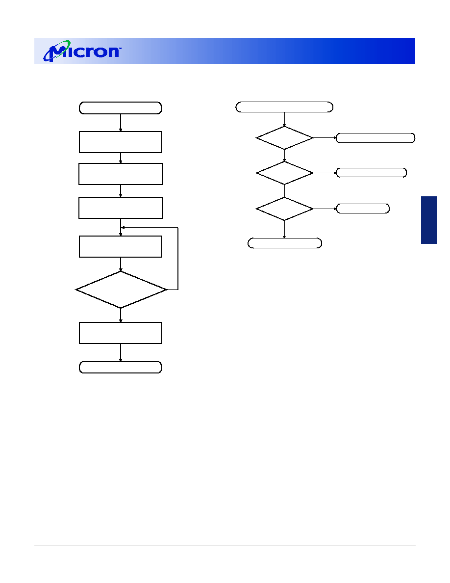
FLASH
31
4 Meg x 16 SyncFlash
Micron Technology, Inc., reserves the right to change products or specifications without notice.
MT28S4M16LC_6.p65 ≠ Rev. 6, Pub. 9/01
©2001, Micron Technology, Inc.
4 MEG x 16
SYNCFLASH MEMORY
COMPLETE PROGRAM STATUS-CHECK
SEQUENCE
SELF-TIMED PROGRAM SEQUENCE
1
NOTE: 1. Sequence may be repeated for multiple PROGRAMs.
2. Complete status check is not required.
3. The bank will be in array read mode.
4. Status register bits 3≠5 must be cleared using CLEAR STATUS REGISTER.
LOAD COMMAND
REGISTER 40h
Start
WRITE
Column Address/Data
Status Register
Polling
SR7 = 1?
Complete Status
Check (optional)
PROGRAM Complete
3
2
ACTIVE Row Address
NO
YES
Start (PROGRAM completed)
SR4, 5 = 1?
YES
Command Sequence Error
SR4 = 1?
NO
YES
NO
YES
NO
4
PROGRAM Successful
SR3 = 1?
Invalid PROGRAM Error
4
PROGRAM Error
4

FLASH
32
4 Meg x 16 SyncFlash
Micron Technology, Inc., reserves the right to change products or specifications without notice.
MT28S4M16LC_6.p65 ≠ Rev. 6, Pub. 9/01
©2001, Micron Technology, Inc.
4 MEG x 16
SYNCFLASH MEMORY
SELF-TIMED BLOCK ERASE SEQUENCE
1
COMPLETE BLOCK ERASE
STATUS-CHECK SEQUENCE
NOTE: 1. Sequence may be repeated to erase multiple blocks.
2. Complete status check is not required.
3. The bank will be in the array read mode.
4. Status register bits 3≠5 must be cleared using CLEAR STATUS REGISTER.
LOAD COMMAND
REGISTER 20h
ACTIVE Row Address
Start
WRITE D0h
Status Register
SR7 = 1
Complete Status
Check (optional)
ERASE Complete
3
2
YES
YES
NO
Block
Protected?
RP# = V
HH
NO
Start (ERASE or BLOCK UNPROTECT completed)
SR4, 5 = 1?
YES
Command Sequence Error
SR5 = 1?
NO
YES
NO
YES
NO
4
BLOCK ERASE or
UNPROTECT Error
4
ERASE or BLOCK UNPROTECT Successful
SR3 = 1?
Invalid ERASE or
UNPROTECT Error
4

FLASH
33
4 Meg x 16 SyncFlash
Micron Technology, Inc., reserves the right to change products or specifications without notice.
MT28S4M16LC_6.p65 ≠ Rev. 6, Pub. 9/01
©2001, Micron Technology, Inc.
4 MEG x 16
SYNCFLASH MEMORY
BLOCK PROTECT SEQUENCE
1
COMPLETE BLOCK
STATUS-CHECK SEQUENCE
NOTE: 1. Sequence may be repeated for multiple BLOCK PROTECTs.
2. Complete status check is not required.
3. The bank will be in array read mode.
4. Status register bits 3≠5 must be cleared using CLEAR STATUS REGISTER.
YES
NO
LOAD COMMAND
REGISTER 60h
ACTIVE Row
Start
WRITE 01h
Status Register
SR7 = 1
Complete Status
Check (optional)
BLOCK PROTECT Complete
3
2
YES
NO
Device
Protected?
RP# = V
HH
Start (BLOCK or DEVICE PROTECT completed)
SR4 = 1?
BLOCK or DEVICE
PROTECT Error
4
BLOCK or DEVICE PROTECT Successful
SR3 = 1?
Invalid BLOCK/DEVICE
PROTECT Error
4
SR4, 5 = 1?
YES
Command Sequence Error
4
NO
YES
NO
YES
NO

FLASH
34
4 Meg x 16 SyncFlash
Micron Technology, Inc., reserves the right to change products or specifications without notice.
MT28S4M16LC_6.p65 ≠ Rev. 6, Pub. 9/01
©2001, Micron Technology, Inc.
4 MEG x 16
SYNCFLASH MEMORY
DEVICE PROTECT SEQUENCE
1
BLOCK UNPROTECT SEQUENCE
NOTE: 1. Once the device protect bit is set, it cannot be reset.
2. Complete status check is not required.
3. For complete details, see Complete Block Status Check Sequence.
4. The device will remain in the array read mode; a READ may be issued to any bank after the WRITE (D0h) is registered.
YES
NO
LOAD COMMAND
REGISTER 60h
ACTIVE Row
Start
WRITE D0h
Status Register
Complete Status
Check (optional)
ALL BLOCKS UNPROTECT Complete
4
2, 3
Device
Protected?
Unprotect
Block 0 or
Block 15?
Block 0
or Block 15
Protected?
RP# = V
HH
NO
NO
NO
YES
YES
YES
SR7 = 1
LOAD COMMAND
REGISTER 60h
Start
WRITE F1h
Complete Status
Check (optional)
DEVICE PROTECT Complete
2, 3
ACTIVE Row
RP# = V
HH
YES
NO
Status Register
SR7 = 1
FLASH
35
4 Meg x 16 SyncFlash
Micron Technology, Inc., reserves the right to change products or specifications without notice.
MT28S4M16LC_6.p65 ≠ Rev. 6, Pub. 9/01
©2001, Micron Technology, Inc.
4 MEG x 16
SYNCFLASH MEMORY
ELECTRICAL CHARACTERISTICS AND RECOMMENDED DC OPERATING CONDITIONS
(Notes: 1, 2); Commercial Temperature (0∫C
T
A
+70∫C)
PARAMETER/CONDITION
SYMBOL
MIN
MAX
UNITS NOTES
V
CC
SUPPLY VOLTAGE
V
CC
3.0
3.6
V
V
CC
Q SUPPLY VOLTAGE
V
CC
Q
3.0
3.6
V
HARDWARE PROTECTION VOLTAGE
V
HH
8.5
10
V
(RP# only)
INPUT HIGH VOLTAGE:
V
IH
2
V
CC
Q + 0.3
V
Logic 1; All Inputs
INPUT LOW VOLTAGE:
V
IL
- 0.3
0.8
V
Logic 0; All Inputs
INPUT LEAKAGE CURRENT:
Any input 0V
V
IN
V
CC
I
L
-5
5
µA
(All other pins not under test = 0V)
OUPUT LEAKAGE CURRENT:
I
OZ
-5
5
µA
DQs are disabled; 0V
V
OUT
V
CC
Q
OUTPUT LEVELS:
Output High Voltage
(I
OUT
= -4mA)
V
OH
2.4
V
(I
OUT
= -100mA)
V
OH
V
Output Low Voltage
(I
OUT
= -4mA)
V
OL
0.4
V
(I
OUT
= 100mA)
V
OL
V
ABSOLUTE MAXIMUM RATINGS*
Voltage on RP# Relative to V
SS
.................... -1V to +10V
Voltage on V
CC
, V
CC
P or V
CC
Q Supply or Inputs,
Relative to V
SS
....................................... -1V to +3.6V
Voltage on I/O Pins Relative to V
SS
.............. V
CC
Q ±0.3V
Operating Temperature,
T
A
(ambient) ........................................ 0∫C to +70∫C
Storage Temperature (plastic) ........... -55∫C to +150∫C
Power Dissipation ........................................................ 1W
Short Circuit Output Current ................................ 50mA
*Stresses greater than those listed under "Absolute
Maximum Ratings" may cause permanent damage to
the device. This is a stress rating only and functional
operation of the device at these or any other conditions
above those indicated in the operational sections of
this specification is not implied. Exposure to absolute
maximum rating conditions for extended periods may
affect reliability.
NOTE: 1. All voltages referenced to V
SS
.
2. An initial pause of 100µs is required after power-up. (V
CC
, V
CC
P and V
CC
Q must be powered up simultaneously. V
SS
and
V
SS
Q must be at same potential.)
FLASH
36
4 Meg x 16 SyncFlash
Micron Technology, Inc., reserves the right to change products or specifications without notice.
MT28S4M16LC_6.p65 ≠ Rev. 6, Pub. 9/01
©2001, Micron Technology, Inc.
4 MEG x 16
SYNCFLASH MEMORY
CAPACITANCE
PARAMETER
SYMBOL
MIN
MAX UNITS NOTES
Input Capacitance: CLK
C
I
1
2.5
6.5
p F
7
Input Capacitance: All other input-only pins
C
I
2
2.5
6.5
p F
7
Input/Output Capacitance: DQs
C
IO
4.0
7.0
p F
7
NOTE: 1. All voltages referenced to V
SS
.
2. An initial pause of 100µs is required after power-up. (V
CC
, V
CC
P, and V
CC
Q must be powered up simultaneously. V
SS
and
V
SS
Q must be at same potential.)
3. I
CC
specifications are tested after the device is properly initialized.
4. I
CC
is dependent on output loading and cycle rates. Specified values are obtained with minimum cycle time and the
outputs open.
5. The I
CC
current will decrease as the CAS latency is reduced. This is due to the fact that the maximum cycle rate is
slower as the CAS latency is reduced.
6. Address transitions average one transition every 30ns.
7. This parameter is sampled. V
CC
= V
CC
Q; f = 1 MHz, T
A
= +25∫C.
I
CC
SPECIFICATIONS AND CONDITIONS
(Notes: 1, 2, 3); Commercial Temperature (0∫C
T
A
+70∫C)
MAX
PARAMETER/CONDITION
SYMBOL
-10
-12
UNITS NOTES
V
CC
OPERATING CURRENT:
I
CCR
1
125
120
mA
4,5,6
Active Mode; Burst = 2; READ;
t
CK = 15ns;
t
RC =
t
RC (MIN);
CAS latency = 3
V
CC
OPERATING CURRENT:
I
CCR
2
100
95
mA
4, 5, 6
Burst Mode; Continuous Burst;
All banks active; READ;
t
CK = 15ns; CAS latency = 3
V
CC
STANDBY CURRENT:
I
CCS
1
10
10
mA
Active Mode; CKE = LOW; Burst in progress
V
CC
STANDBY CURRENT:
I
CCS
2
2
2
mA
Power-Down Mode; CKE = LOW; No burst in progress
V
CC
DEEP POWER-DOWN CURRENT:
I
CCDP
300
300
µA
RP# = V
SS
±0.2V
PROGRAM CURRENT
I
CCW
+ I
PPW
60
60
mA
V
CC
P OPERATING CURRENT:
I
PPR
1
250
125
µA
Active Mode; Burst = 2; READ;
t
RC =
t
RC (MIN); CAS latency = 3
V
CC
P OPERATING CURRENT:
I
CC
E
+I
PP
E
80
80
mA
ERASE CURRENT
V
CC
P DEEP POWER-DOWN CURRENT:
I
PPDP
1
1
µA
RP# = V
SS
±0.2V
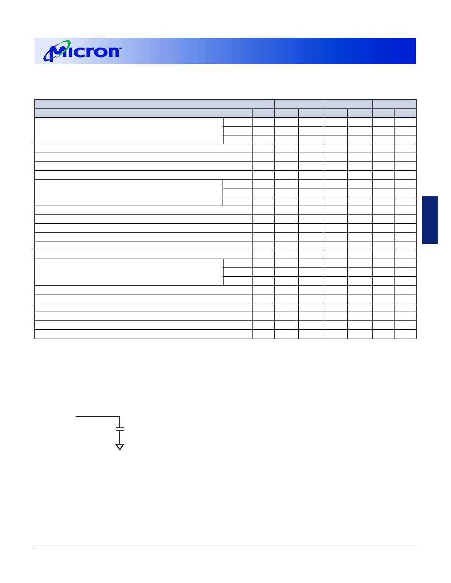
FLASH
37
4 Meg x 16 SyncFlash
Micron Technology, Inc., reserves the right to change products or specifications without notice.
MT28S4M16LC_6.p65 ≠ Rev. 6, Pub. 9/01
©2001, Micron Technology, Inc.
4 MEG x 16
SYNCFLASH MEMORY
ELECTRICAL CHARACTERISTICS AND RECOMMENDED AC OPERATING CONDITIONS
(Notes: 1, 2, 3, 4, 5); Commercial Temperature (0∫C
T
A
+70∫C)
AC CHARACTERISTICS
-10
-12
PARAMETER
SYM
MIN
MAX
MIN
MAX
UNITS NOTES
Access time from CLK (pos. edge)
CL = 3
t
AC
7
9
ns
CL = 2
t
AC
9
10
ns
CL = 1
t
AC
27
27
ns
Address hold time
t
AH
2
2
ns
Address setup time
t
AS
3
3
ns
CLK high level width
t
CH
3.5
4
ns
CLK low level width
t
CL
3.5
4
ns
Clock cycle time
CL = 3
t
CK
10
12
ns
CL = 2
t
CK
15
15
ns
CL = 1
t
CK
30
30
ns
CKE hold time
t
CKH
2
2
ns
CKE setup time
t
CKS
3
3
ns
CS#, RAS#, CAS#, WE#, DQM hold time
t
CMH
2
2
ns
CS#, RAS#, CAS#, WE#, DQM setup time
t
CMS
3
3
ns
Data-in hold time
t
DH
2
2
ns
Data-in setup time
t
DS
3
3
ns
Data-out high-impedance time
CL = 3
t
HZ
8
9
ns
6
CL = 2
t
HZ
10
10
ns
6
CL = 1
t
HZ
15
15
ns
6
Data-out low-impedance time
t
LZ
2
2
ns
Data-out hold time
t
OH
3
3
ns
ACTIVE command period
t
RC
90
100
ns
ACTIVE to READ or WRITE delay
t
RCD
30
30
ns
ACTIVE bank A to ACTIVE bank B command
t
RRD
20
20
ns
Transition time
t
T
0.3
1.2
1
1.2
ns
7
NOTE: 1. The minimum specifications are used only to indicate cycle time at which proper operation over the full temperature
range is ensured.
2. An initial pause of 100µs is required after power-up. (V
CC
, V
CC
P, and V
CC
Q must be powered up simultaneously. V
SS
and
V
SS
Q must be at same potential.)
3. In addition to meeting the transition rate specification, the clock and CKE must transit between V
IH
and V
IL
(or between
V
IL
and V
IH
) in a monotonic manner.
4. Outputs measured at 1.5V with equivalent load:
Q
50pF
5. AC timing and I
CC
tests have V
IL
= 0V and V
IH
= 3V, with timing referenced to 1.5V crossover point.
6.
t
HZ defines the time at which the output achieves the open circuit condition; it is not a reference to V
OH
or V
OL
. The
last valid data element will meet
t
OH before going High-Z.
7. AC characteristics assume
t
T = 1ns.
FLASH
38
4 Meg x 16 SyncFlash
Micron Technology, Inc., reserves the right to change products or specifications without notice.
MT28S4M16LC_6.p65 ≠ Rev. 6, Pub. 9/01
©2001, Micron Technology, Inc.
4 MEG x 16
SYNCFLASH MEMORY
AC FUNCTIONAL CHARACTERISTICS
(Notes: 1-6); Commercial Temperature (0∫C
T
A
+70∫C)
PARAMETER
SYMBOL
-10
-12
UNITS
NOTES
READ/WRITE command to READ/LOAD COMMAND REGISTER command
t
CCD
1
1
t
CK
7
CKE to clock disable or power-down entry mode
t
CKED
1
1
t
CK
8
CKE to clock enable or power-down exit setup mode
t
PED
1
1
t
CK
8
DQM to input data delay
t
DQD
0
0
t
CK
7
DQM to data mask during WRITEs
t
DQM
0
0
t
CK
7
DQM to data high-impedance during READs
t
DQZ
2
2
t
CK
7
WRITE command to input data delay
t
DWD
0
0
t
CK
7
Data-in to ACTIVE command
t
DAL
4
4
t
CK
Data-in to ACTIVE TERMINATE command
t
DPL
1
1
t
CK
LOAD MODE REGISTER command to ACTIVE command
t
MRD
2
2
t
CK
7
Data-out to High-Z from ACTIVE TERMINATE command
CL = 3
t
ROH
3
3
t
CK
7
CL = 2
t
ROH
2
2
t
CK
7
CL = 1
t
ROH
1
1
t
CK
7
NOTE: 1. The minimum specifications are used only to indicate cycle time at which proper operation over the full temperature
range is ensured.
2. An initial pause of 100µs is required after power-up. (V
CC
, V
CC
P, and V
CC
Q must be powered up simultaneously. V
SS
and
V
SS
Q must be at same potential.)
3. AC characteristics assume
t
T = 1ns.
4. In addition to meeting the transition rate specification, the clock and CKE must transit between V
IH
and V
IL
(or between
V
IL
and V
IH
) in a monotonic manner.
5. Outputs measured at 1.5V with equivalent load:
Q
50pF
6. AC timing and I
CC
tests have V
IL
= 0V and V
IH
= 3V, with timing referenced to 1.5V crossover point.
7. Required clocks specified by JEDEC functionality and not dependent on any timing parameter.
8. Timing actually specified by
t
CKS; clock(s) specified as a reference only at minimum cycle rate.
ERASE AND PROGRAM TIMING
CHARACTERISTICS
Commercial Temperature (0∫C
£ T
A
£ +70∫C)
-10/-12
PARAMETER
MIN
MAX UNITS
Word program time
5
5,000
µs
Block erase time
1.1
13
s
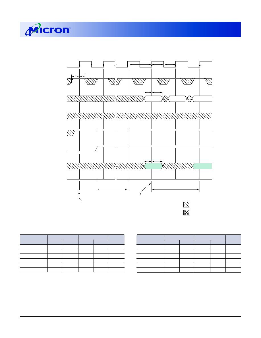
39
4 Meg x 16 SyncFlash
Micron Technology, Inc., reserves the right to change products or specifications without notice.
MT28S4M16LC_6.p65 ≠ Rev. 6, Pub. 9/01
©2001, Micron Technology, Inc.
4 MEG x 16
SYNCFLASH MEMORY
INITIALIZE AND LOAD MODE REGISTER
*CAS latency indicated in parentheses.
TIMING PARAMETERS
-10
-12
SYMBOL*
MIN
MAX
MIN
MAX
UNITS
t
AH
2
2
ns
t
AS
3
3
ns
t
CH
3.5
4
ns
t
CL
3.5
4
ns
t
CK (3)
10
12
ns
t
CK (2)
15
15
ns
-10
-12
SYMBOL*
MIN
MAX
MIN
MAX
UNITS
t
CK (1)
30
30
ns
t
CKH
2
2
ns
t
CKS
3
3
ns
t
CMH
2
2
ns
t
CMS
3
3
ns
t
MRD
2
2
t
CK
NOTE: 1. RP# = V
HH
or V
IH
2. V
CC
, V
CC
P, V
CC
Q = 3.3V
3. The nvmode register contents are automatically loaded into the mode register upon power-up initialization, LOAD
MODE REGISTER cycle is required to enter new mode register values.
4. JEDEC and PC100 specify three clocks.
5. If CS is HIGH at clock time, all commands applied are NOP, with CKE a "Don't Care."
tCH
tCL
CKE
T0
CLK
T1
Tn + 3
Tn + 4
COMMAND
DQ
ADDRESS
OPCODE
tMRD
Program Mode Register
3, 4, 5
tCMS
Power-up:
2
V
CC
, V
CC
P, V
CC
Q,
CLK stable
T = 100µs
tAH
tAS
ROW
LOAD MODE
REGISTER
NOP
ACTIVE
High-Z
DQM
V
CC
, V
CC
P,
V
CC
Q
DON'T CARE
UNDEFINED
Tn+1
Tn + 2
tCK
tCMH
tCKH
tCKS
(
)
(
)
(
)
(
)
(
)
(
)
(
)
(
)
(
)
(
)
(
)
(
)
(
)
(
)
(
)
(
)
(
)
(
)
(
)
(
)
RP#
1
(
)
(
)
(
)
(
)
(
)
(
)
(
)
(
)
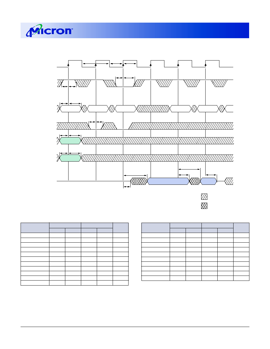
40
4 Meg x 16 SyncFlash
Micron Technology, Inc., reserves the right to change products or specifications without notice.
MT28S4M16LC_6.p65 ≠ Rev. 6, Pub. 9/01
©2001, Micron Technology, Inc.
4 MEG x 16
SYNCFLASH MEMORY
t
CKS
3
3
ns
t
CMH
2
2
ns
t
CMS
3
3
ns
t
DH
2
2
ns
t
DS
3
3
ns
t
HZ (3)
8
9
ns
t
HZ (2)
10
10
ns
t
HZ (1)
15
15
ns
t
LZ
2
2
ns
t
OH
3
3
ns
CLOCK SUSPEND MODE
1
*CAS latency indicated in parentheses.
TIMING PARAMETERS
-10
-12
SYMBOL*
MIN
MAX
MIN
MAX
UNITS
t
AC (3)
7
9
ns
t
AC (2)
9
10
ns
t
AC (1)
27
27
ns
t
AH
2
2
ns
t
AS
3
3
ns
t
CH
3.5
4
ns
t
CL
3.5
4
ns
t
CK (3)
10
12
ns
t
CK (2)
15
15
ns
t
CK (1)
30
30
ns
t
CKH
2
2
ns
-10
-12
SYMBOL*
MIN
MAX
MIN
MAX
UNITS
NOTE: 1. For this example, the burst length = 2, CAS latency = 3.
2. x16: A0≠A7.
tCH
tCL
tCK
tAC
tLZ
DQM
CLK
A0≠A11
DQ
BA
tOH
D
OUT
m
tAH
tAS
tAH
tAS
tAC
tHZ
D
OUT
m+1
COMMAND
tCMH
tCMS
tCMH
tCMS
NOP
NOP
NOP
NOP
NOP
READ
DON'T CARE
UNDEFINED
CKE
tCKS tCKH
BANK
COLUMN m
2
tCKH
tCKS
T0
T1
T2
T3
T4
T5
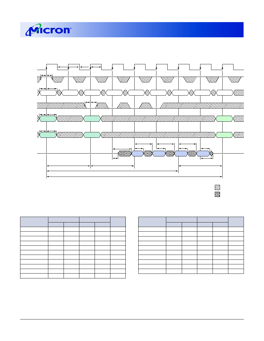
41
4 Meg x 16 SyncFlash
Micron Technology, Inc., reserves the right to change products or specifications without notice.
MT28S4M16LC_6.p65 ≠ Rev. 6, Pub. 9/01
©2001, Micron Technology, Inc.
4 MEG x 16
SYNCFLASH MEMORY
READ
1
t
CKS
3
3
ns
t
CMH
2
2
ns
t
CMS
3
3
ns
t
HZ (3)
8
9
ns
t
HZ (2)
10
10
ns
t
HZ (1)
15
15
ns
t
LZ
2
2
ns
t
OH
3
3
ns
t
RC
90
100
ns
t
RCD
30
30
ns
*CAS latency indicated in parentheses.
TIMING PARAMETERS
-10
-12
SYMBOL*
MIN
MAX
MIN
MAX
UNITS
t
AC (3)
7
9
ns
t
AC (2)
9
10
ns
t
AC (1)
27
27
ns
t
AH
2
2
ns
t
AS
3
3
ns
t
CH
3.5
4
ns
t
CL
3.5
4
ns
t
CK (3)
10
12
ns
t
CK (2)
15
15
ns
t
CK (1)
30
30
ns
t
CKH
2
2
ns
-10
-12
SYMBOL*
MIN
MAX
MIN
MAX
UNITS
NOTE: 1. For this example, the burst length = 4, CAS latency = 2.
2. x16: A0≠A7.
3.
t
RAS and
t
RP are referenced to show compatibility with SDRAM timings; no values are given.
tCH
tCL
tCK
tAC
tLZ
tRP
3
tRAS
3
tRCD
CAS Latency
tRC
DQM
CKE
CLK
A0≠A11
DQ
BA
tOH
D
OUT
m
tAH
tAS
tAH
tAS
COLUMN m
2
ROW
BANK
BANK
ROW
BANK
DON'T CARE
UNDEFINED
tHZ
tOH
D
OUT
m+3
tAC
tOH
tAC
tOH
tAC
D
OUT
m+2
D
OUT
m+1
COMMAND
tCMH
tCMS
tCMH
tCMS
NOP
NOP
NOP
ACTIVE
NOP
READ
NOP
ACTIVE
NOP
tCKH
tCKS
T0
T1
T2
T3
T4
T5
T6
T7
T8
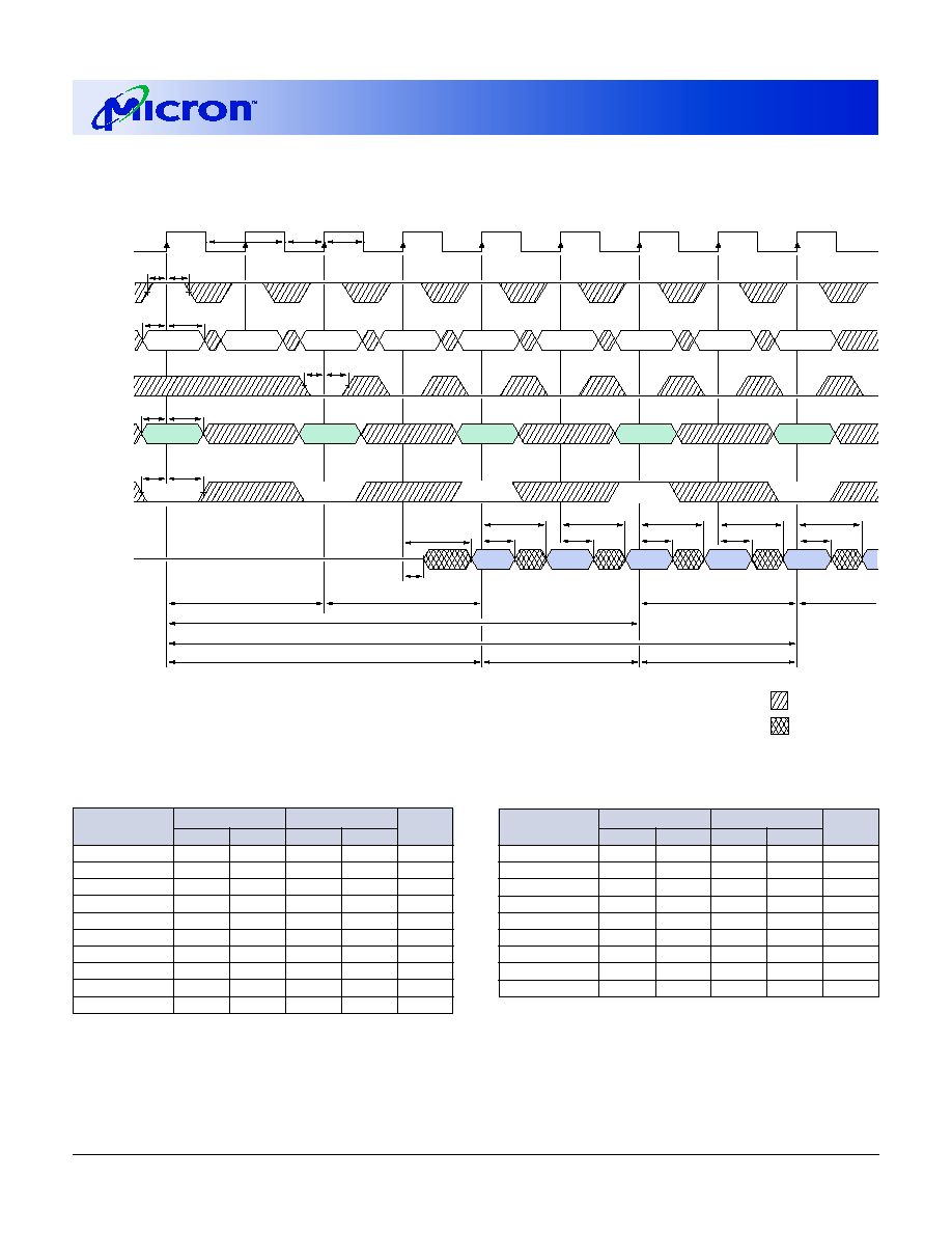
42
4 Meg x 16 SyncFlash
Micron Technology, Inc., reserves the right to change products or specifications without notice.
MT28S4M16LC_6.p65 ≠ Rev. 6, Pub. 9/01
©2001, Micron Technology, Inc.
4 MEG x 16
SYNCFLASH MEMORY
ALTERNATING BANK READ ACCESSES
1
t
CKH
2
2
ns
t
CKS
3
3
ns
t
CMH
2
2
ns
t
CMS
3
3
ns
t
LZ
2
2
ns
t
OH
3
3
ns
t
RC
90
100
ns
t
RCD
30
30
ns
t
RRD
20
20
ns
*CAS latency indicated in parentheses.
TIMING PARAMETERS
-10
-12
SYMBOL*
MIN
MAX
MIN
MAX
UNITS
t
AC (3)
7
9
ns
t
AC (2)
9
10
ns
t
AC (1)
27
27
ns
t
AH
2
2
ns
t
AS
3
3
ns
t
CH
3.5
4
ns
t
CL
3.5
4
ns
t
CK (3)
10
12
ns
t
CK (2)
15
15
ns
t
CK (1)
30
30
ns
-10
-12
SYMBOL*
MIN
MAX
MIN
MAX
UNITS
NOTE: 1. For this example, CAS latency = 2.
2. x16: A0≠A7.
tCH
tCL
tCK
tAC
tLZ
DQM
CLK
A0≠A11
DQ
BA
tOH
D
OUT
m
tAH
tAS
tAH
tAS
COLUMN m
2
ROW
ROW
DON'T CARE
UNDEFINED
tOH
D
OUT
m+3
tAC
tOH
tAC
tOH
tAC
D
OUT
m+2
D
OUT
m+1
COMMAND
tCMH
tCMS
tCMH
tCMS
NOP
NOP
ACTIVE
NOP
READ
NOP
ACTIVE
tOH
D
OUT
b
tAC
tAC
READ
COLUMN b
2
ACTIVE
ROW
BANK 0
BANK 0
BANK 1
BANK 1
BANK 0
CKE
tCKH
tCKS
tRP - BANK 0
tRAS - BANK 0
tRCD - BANK 0
tRCD - BANK 0
CAS Latency - BANK 0
tRCD - BANK 1
CAS Latency - BANK 1
t
t
RC - BANK 0
RRD
T0
T1
T2
T3
T4
T5
T6
T7
T8

43
4 Meg x 16 SyncFlash
Micron Technology, Inc., reserves the right to change products or specifications without notice.
MT28S4M16LC_6.p65 ≠ Rev. 6, Pub. 9/01
©2001, Micron Technology, Inc.
4 MEG x 16
SYNCFLASH MEMORY
READ ≠ FULL-PAGE BURST
1
t
CKH
2
2
ns
t
CKS
3
3
ns
t
CMH
2
2
ns
t
CMS
3
3
ns
t
HZ (3)
8
9
ns
t
HZ (2)
10
10
ns
t
HZ (1)
15
15
ns
t
LZ
2
2
ns
t
OH
3
3
ns
t
RCD
30
30
ns
*CAS latency indicated in parentheses.
TIMING PARAMETERS
-10
-12
SYMBOL*
MIN
MAX
MIN
MAX
UNITS
t
AC (3)
7
9
ns
t
AC (2)
9
10
ns
t
AC (1)
27
27
ns
t
AH
2
2
ns
t
AS
3
3
ns
t
CH
3.5
4
ns
t
CL
3.5
4
ns
t
CK (3)
10
12
ns
t
CK (2)
15
15
ns
t
CK (1)
30
30
ns
-10
-12
SYMBOL*
MIN
MAX
MIN
MAX
UNITS
NOTE: 1. For this example, the CAS latency = 2.
2. x16: A0≠A7.
tCH
tCL
tCK
tAC
tLZ
tRCD
CAS Latency
DQM
CKE
CLK
A0≠A11
DQ
BA
OH
D
OUT
m
tAH
tAS
tAC
tOH
D
OUT
m+1
ROW
tHZ
tAC
tOH
D
OUT
m+1
tAC
tOH
D
OUT
m+2
tAC
tOH
D
OUT
m-1
tAC
tOH
D
OUT
m
Full-page burst does not self-terminate.
Can use BURST TERMINATE command.
(
)
(
)
(
)
(
)
(
)
(
)
(
)
(
)
(
)
(
)
(
)
(
)
(
)
(
)
Full page completed.
256 (x16) locations within
the same row.
DON'T CARE
UNDEFINED
COMMAND
tCMH
tCMS
tCMH
tCMS
NOP
NOP
NOP
ACTIVE
NOP
READ
NOP
BURST TERM
NOP
NOP
(
)
(
)
(
)
(
)
NOP
COLUMN m
2
tAH
tAS
BANK
(
)
(
)
(
)
(
)
BANK
tCKH
tCKS
(
)
(
)
(
)
(
)
(
)
(
)
(
)
(
)
T0
T1
T2
T3
T4
T5
T6
Tn + 1
Tn + 2
Tn + 3
Tn + 4
3
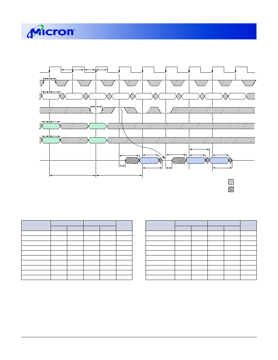
44
4 Meg x 16 SyncFlash
Micron Technology, Inc., reserves the right to change products or specifications without notice.
MT28S4M16LC_6.p65 ≠ Rev. 6, Pub. 9/01
©2001, Micron Technology, Inc.
4 MEG x 16
SYNCFLASH MEMORY
READ ≠ DQM OPERATION
1
t
CKH
2
2
ns
t
CKS
3
3
ns
t
CMH
2
2
ns
t
CMS
3
3
ns
t
HZ (3)
8
9
ns
t
HZ (2)
10
10
ns
t
HZ (1)
15
15
ns
t
LZ
2
2
ns
t
OH
3
3
ns
t
RCD
30
30
ns
*CAS latency indicated in parentheses.
TIMING PARAMETERS
-10
-12
SYMBOL*
MIN
MAX
MIN
MAX
UNITS
t
AC (3)
7
9
ns
t
AC (2)
9
10
ns
t
AC (1)
27
27
ns
t
AH
2
2
ns
t
AS
3
3
ns
t
CH
3.5
4
ns
t
CL
3.5
4
ns
t
CK (3)
10
12
ns
t
CK (2)
15
15
ns
t
CK (1)
30
30
ns
-10
-12
SYMBOL*
MIN
MAX
MIN
MAX
UNITS
NOTE: 1. For this example, the burst length = 4, CAS latency = 2.
2. x16: A0≠A7.
tCH
tCL
tCK
tRCD
CAS Latency
DQM
CKE
CLK
A0≠A11
DQ
BA
BANK
ROW
BANK
DON'T CARE
UNDEFINED
tAC
LZ
D
OUT
m
tOH
D
OUT
m+3
D
OUT
m+2
t
tHZ
LZ
t
COMMAND
NOP
NOP
NOP
ACTIVE
NOP
READ
NOP
NOP
NOP
tHZ
tAC
tOH
tAC
tOH
tAH
tAS
tAH
tAS
tCMS tCMH
tCMS tCMH
COLUMN m
2
tCKH
tCKS
T0
T1
T2
T3
T4
T5
T6
T7
T8

45
4 Meg x 16 SyncFlash
Micron Technology, Inc., reserves the right to change products or specifications without notice.
MT28S4M16LC_6.p65 ≠ Rev. 6, Pub. 9/01
©2001, Micron Technology, Inc.
4 MEG x 16
SYNCFLASH MEMORY
NOTE: 1. For this example, READ burst length = 2, CAS = 3.
2. Com-code = 40h for WRITE, 20h for ERASE (see Truth Table 2).
3. Column address is "Don't Care" for ERASE operation.
4. D
IN
= D0h (erase confirm) for ERASE operation.
PROGRAM/ERASE
1
(BANK a FOLLOWED BY READ TO BANK b)
t
CKH
2
2
ns
t
CKS
3
3
ns
t
CMH
2
2
ns
t
CMS
3
3
ns
t
DH
2
1.5
ns
t
DS
3
3
ns
TIMING PARAMETERS
-10
-12
SYMBOL*
MIN
MAX
MIN
MAX
UNITS
t
AH
2
2
ns
t
AS
3
3
ns
t
CH
3.5
4
ns
t
CL
3.5
4
ns
t
CK (3)
10
12
ns
t
CK (2)
15
15
ns
t
CK (1)
30
30
ns
-10
-12
SYMBOL*
MIN
MAX
MIN
MAX
UNITS
*CAS latency indicated in parentheses.
tCH
tCL
tCK
DQM
CKE
CLK
A0
≠
A11
BA
DQ
tCMH
tCMS
BANK b
ROW
BANK a
D
IN4
m
tDH
tDS
tDS
COMMAND
tCMH
tCMS
READ
NOP
ACTIVE
NOP
WRITE
LCR
NOP
BANK a
COLUMN n
BANK a
tAH
tAS
tDH
tCKH
tCKS
NOP
NOP
NOP
COLUMN3 m
T0
T1
T2
T3
T4
T5
T6
T7
T8
T9
COMCODE2
DON'T CARE
UNDEFINED
tRCD
D
OUT
n
D
OUT
n + 1
High-Z

46
4 Meg x 16 SyncFlash
Micron Technology, Inc., reserves the right to change products or specifications without notice.
MT28S4M16LC_6.p65 ≠ Rev. 6, Pub. 9/01
©2001, Micron Technology, Inc.
4 MEG x 16
SYNCFLASH MEMORY
PROGRAM/ERASE
1
(BANK a FOLLOWED BY READ TO BANK a)
tCH
tCL
tCK
DQM
CKE
CLK
A0≠A11
BA
DQ
tAH
tAS
BANK a
ROW
BANK a
DON'T CARE
UNDEFINED
D
IN5
m
tDH
tDS
COMMAND
tCMH
tCMS
ACTIVE
NOP
WRITE
LCR
BANK a
tAH
tAS
tCKH
tCKS
COLUMN4 m
T0
T1
T2
T3
COMCODE2
ISM PROGRAM or ERASE
operation is complete
T = 1
0µs
typical/word
tCMH
tCMS
READ
NOP
COLUMN n
NOP
T4
T5
T6
tDS t
ROW
COLUMN
BANK a
BANK a
High-Z
SR7 = 1
SR7 = 0
Tn
Tn + 1
Tn + 2
Tn + 3
BANK a
DH
D
OUT
n
D
OUT
NOP
ACTIVE
NOP
READ
NOP
NOP
NOP
Tn + 4
Tn + 5
NOP
READ
3
NOTE: 1. ACTIVE/READ or READ will output the contents of the row activated prior to the LCR/active/write command sequence. This example illustrates the
timing for activating a new row in bank a. For this example, READ burst length = 2, CAS latency = 2.
2. Com-code = 40h for PROGRAM, 20h for ERASE (see Truth Table 2).
3. LCR/ACTIVE cycles must be initiated prior to READ according to Truth Table 2 for a status register read command sequence.
4. Column address is "Don't Care" for ERASE operation.
5. D
IN
= D0h (erase confirm) for ERASE operation.
t
CKH
2
2
ns
t
CKS
3
3
ns
t
CMH
2
2
ns
t
CMS
3
3
ns
t
DH
2
2
ns
t
DS
3
3
ns
TIMING PARAMETERS
-10
-12
SYMBOL*
MIN
MAX
MIN
MAX
UNITS
t
AH
2
2
ns
t
AS
3
3
ns
t
CH
3.5
4
ns
t
CL
3.5
4
ns
t
CK (3)
10
12
ns
t
CK (2)
15
15
ns
t
CK (1)
30
30
ns
-10
-12
SYMBOL*
MIN
MAX
MIN
MAX
UNITS
*CAS latency indicated in parentheses.
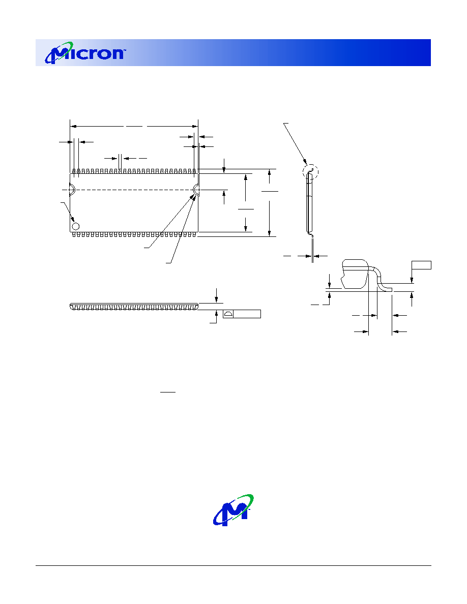
47
4 Meg x 16 SyncFlash
Micron Technology, Inc., reserves the right to change products or specifications without notice.
MT28S4M16LC_6.p65 ≠ Rev. 6, Pub. 9/01
©2001, Micron Technology, Inc.
4 MEG x 16
SYNCFLASH MEMORY
54-PIN TSOP TYPE II
(400 MIL)
SEE DETAIL A
.20
.05
1.00 (2X)
.75 (2X)
.80 TYP
.71
10.24
10.08
.18
.13
.60
.40
PIN #1 ID
DETAIL A
22.30
22.14
.45
.30
1.2 MAX
.10
.25
11.86
11.66
.80
TYP
.10 (2X)
2.80
NOTE: 1. All dimensions in millimeters MAX or typical where noted.
MIN
2. Package width and length do not include mold protrusion; allowable mold protrusion is 0.25mm per side.
8000 S. Federal Way, P.O. Box 6, Boise, ID 83707-0006, Tel: 208-368-3900
E-mail: prodmktg@micron.com, Internet: http://www.micron.com, Customer Comment Line: 800-932-4992
Micron and SyncFlash are registered trademarks and the Micron logo, and M logo are trademarks of Micron Technology, Inc.
DATA SHEET DESIGNATION
This data sheet contains minimum and maximum limits specified over the complete power supply and
temperature range for production devices. Although considered final, these specifications are subject to change,
as further product development and data characterization sometimes occur.

48
4 Meg x 16 SyncFlash
Micron Technology, Inc., reserves the right to change products or specifications without notice.
MT28S4M16LC_6.p65 ≠ Rev. 6, Pub. 9/01
©2001, Micron Technology, Inc.
4 MEG x 16
SYNCFLASH MEMORY
REVISION HISTORY
Rev. 6 ......................................................................................................................................................................... 9/01
∑ Added erase and program timing characteristics
∑ Updated the device protect sequence
∑ Removed the "Preliminary" designation
Rev. 5, PRELIMINARY .............................................................................................................................................. 7/01
Changed
t
AH,
t
CKH,
t
CMH,
t
DH from 1ns to 2ns
Rev. 4, ADVANCE .................................................................................................................................................... 5/01
Changed deep power-down current from 100µA to 300µA
Rev. 3, ADVANCE .................................................................................................................................................... 4/01
Changes to V
CC
P Operating Current
Changes to MAX Capacitance Parameters
Rev. 2, ADVANCE .................................................................................................................................................... 2/01
Changes to Absolute Maximum Ratings
Changes to I
CC
Specifications and Conditions
Original document, Rev. 11/00, ADVANCE ......................................................................................................... 11/00