 | –≠–Ľ–Ķ–ļ—ā—Ä–ĺ–Ĺ–Ĺ—č–Ļ –ļ–ĺ–ľ–Ņ–ĺ–Ĺ–Ķ–Ĺ—ā: MT46V32M8 | –°–ļ–į—á–į—ā—Ć:  PDF PDF  ZIP ZIP |

PRODUCTS AND SPECIFICATIONS DISCUSSED HEREIN ARE SUBJECT TO CHANGE BY MICRON WITHOUT NOTICE.
09005aef8076894f
256MBDDRx4x8x16_1.fm - Rev. F 6/03 EN
1
©2003 Micron Technology, Inc.
256Mb: x4, x8, x16
DDR SDRAM
DOUBLE DATA RATE
(DDR) SDRAM
MT46V64M4 ≠ 16 MEG x 4 x 4 BANKS
MT46V32M8 ≠ 8 MEG x 8 x 4 BANKS
MT46V16M16 ≠ 4 MEG x 16 x 4 BANKS
For the latest data sheet revisions, please refer to the
Micron
‚
Web site: www.micron.com/datasheets
Features
∑ V
DD
= +2.5V Ī0.2V, V
DD
Q = +2.5V Ī0.2V
∑ Bidirectional data strobe (DQS) transmitted/received
with data, i.e., source-synchronous data capture (x16 has
two ≠ one per byte)
∑ Internal, pipelined double data rate (DDR) architecture;
two data accesses per clock cycle
∑ Differential clock inputs (CK and CK#)
∑ Commands entered on each positive CK edge
∑ DQS edge-aligned with data for READs; center-aligned
with data for WRITEs
∑ DLL to align DQ and DQS transitions with CK
∑ Four internal banks for concurrent operation
∑ Data mask (DM) for masking write data (x16 has two ≠ one
per byte)
∑ Programmable burst lengths: 2, 4, or 8
∑ Auto Refresh and Self Refresh Modes
∑ Longer-lead TSOP for improved reliability (OCPL)
∑ 2.5V I/O (SSTL_2 compatible)
∑ Concurrent auto precharge option supported
∑
t
RAS lockout supported (
t
RAP =
t
RCD)
NOTE:
1. Contact Micron for availability of lead-free products.
2. Supports PC2700 modules with 2.5-3-3 timing.
3. Supports PC2100 modules with 2-2-2 timing.
4. Supports PC2100 modules with 2-3-3 timing.
5. Supports PC2100 modules with 2.5-3-3 timing.
6. Supports PC1600 modules with 2-2-2 timing.
7. CL=CAS(READ) latency.
8. Minimum clock rate @ CL = 2 (-75E, -75Z), @ CL = 2.5
(-6T, -6R, -75)
OPTIONS
MARKING
∑
Configuration
64 Meg x 4 (16 Meg x 4 x 4 banks)
64M4
32 Meg x 8 (8 Meg x 8 x 4 banks)
32M8
16 Meg x 16 (4 Meg x 16 x 4 banks)
16M16
∑
Plastic Package ≠ OCPL
66-pin TSOP
TG
66-pin TSOP (lead-free)
1
P
∑
Plastic Package
60-Ball FBGA (16mm x 9mm)
FJ
60-Ball FBGA (16mm x 9mm)(lead-free)
1
BJ
60-Ball FBGA (14mm x 8mm)
FG
60-Ball FBGA (14mm x 8mm) (lead-free)
1
BG
∑
Timing ≠ Cycle Time
6ns @ CL = 2.5 (DDR333)
2
(FBGA only)
-6
6ns @ CL = 2.5 (DDR333)
2
(TSOP only)
-6R/-6T
7.5ns @ CL = 2 (DDR266)
3
-75E
7.5ns @ CL = 2 (DDR266A)
4
-75Z
7.5ns @ CL = 2.5 (DDR266B)
5, 6
-75
∑
Self Refresh
Standard
None
Low-Power Self Refresh
L
∑
High-Speed Process Enhancement
Standard
None
High Speed
H
∑
Temperature Rating
Standard (0
įC to +70įC)
None
Industrial Temperature (-40
įC to +85įC)
IT
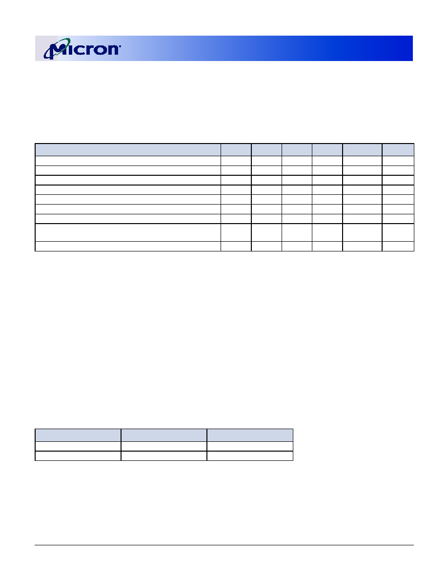
Table 1:
Key Timing Parameters
SPEED
GRADE
CLOCK RATE
7
DATA-OUT
WINDOW
8
ACCESS
WINDOW
DQS≠DQ
SKEW
CL=2
CL=2.5
-6
133 MHz
167 MHz
2.1ns
Ī0.7ns
+0.40ns
-6R/-6T
133 MHz
167 MHz
2.0ns
Ī0.7ns
+0.45ns
-75E/-75Z
133 MHz
133 MHz
2.5ns
Ī0.75ns
+0.5ns
-75
100 MHz
133 MHz
2.5ns
Ī0.75ns
+0.5ns
64 MEG x 4
32 MEG x 8
16 MEG x 16
Configuration
16 Meg x 4 x 4
banks
8 Meg x 8 x 4
banks
4 Meg x 16 x 4
banks
Refresh Count
8K
8K
8K
Row Addressing
8K (A0≠A12)
8K (A0≠A12)
8K (A0≠A12)
Bank Addressing
4 (BA0,BA1)
4 (BA0,BA1)
4 (BA0,BA1)
Column Addressing
2K (A0≠A9,A11)
1K (A0≠A9)
512 (A0≠A8)
1
2
3
4
5
6
7
8
9
10
11
12
13
14
15
16
17
18
19
20
21
22
23
24
25
26
27
28
29
30
31
32
33
66
65
64
63
62
61
60
59
58
57
56
55
54
53
52
51
50
49
48
47
46
45
44
43
42
41
40
39
38
37
36
35
34
V
SS
DQ15
V
SS
Q
DQ14
DQ13
V
DD
Q
DQ12
DQ11
V
SS
Q
DQ10
DQ9
V
DD
Q
DQ8
NC
V
SS
Q
UDQS
DNU
V
REF
V
SS
UDM
CK#
CK
CKE
NC
A12
A11
A9
A8
A7
A6
A5
A4
V
SS
x16
V
DD
DQ0
V
DD
Q
DQ1
DQ2
VssQ
DQ3
DQ4
V
DD
Q
DQ5
DQ6
VssQ
DQ7
NC
V
DD
Q
LDQS
NC
V
DD
DNU
LDM
WE#
CAS#
RAS#
CS#
NC
BA0
BA1
A10/AP
A0
A1
A2
A3
V
DD
x16
V
SS
DQ7
V
SS
Q
NC
DQ6
V
DD
Q
NC
DQ5
V
SS
Q
NC
DQ4
V
DD
Q
NC
NC
V
SS
Q
DQS
DNU
V
REF
V
SS
DM
CK#
CK
CKE
NC
A12
A11
A9
A8
A7
A6
A5
A4
V
SS
x8
x4
V
SS
NC
V
SS
Q
NC
DQ3
V
DD
Q
NC
NC
V
SS
Q
NC
DQ2
V
DD
Q
NC
NC
V
SS
Q
DQS
DNU
V
REF
V
SS
DM
CK#
CK
CKE
NC
A12
A11
A9
A8
A7
A6
A5
A4
V
SS
V
DD
DQ0
V
DD
Q
NC
DQ1
V
SS
Q
NC
DQ2
V
DD
Q
NC
DQ3
V
SS
Q
NC
NC
V
DD
Q
NC
NC
V
DD
DNU
NC
WE#
CAS#
RAS#
CS#
NC
BA0
BA1
A10/AP
A0
A1
A2
A3
V
DD
x8
x4
V
DD
NC
V
DD
Q
NC
DQ0
V
SS
Q
NC
NC
V
DD
Q
NC
DQ1
V
SS
Q
NC
NC
V
DD
Q
NC
NC
V
DD
DNU
NC
WE#
CAS#
RAS#
CS#
NC
BA0
BA1
A10/AP
A0
A1
A2
A3
V
DD
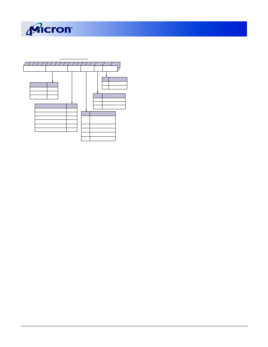
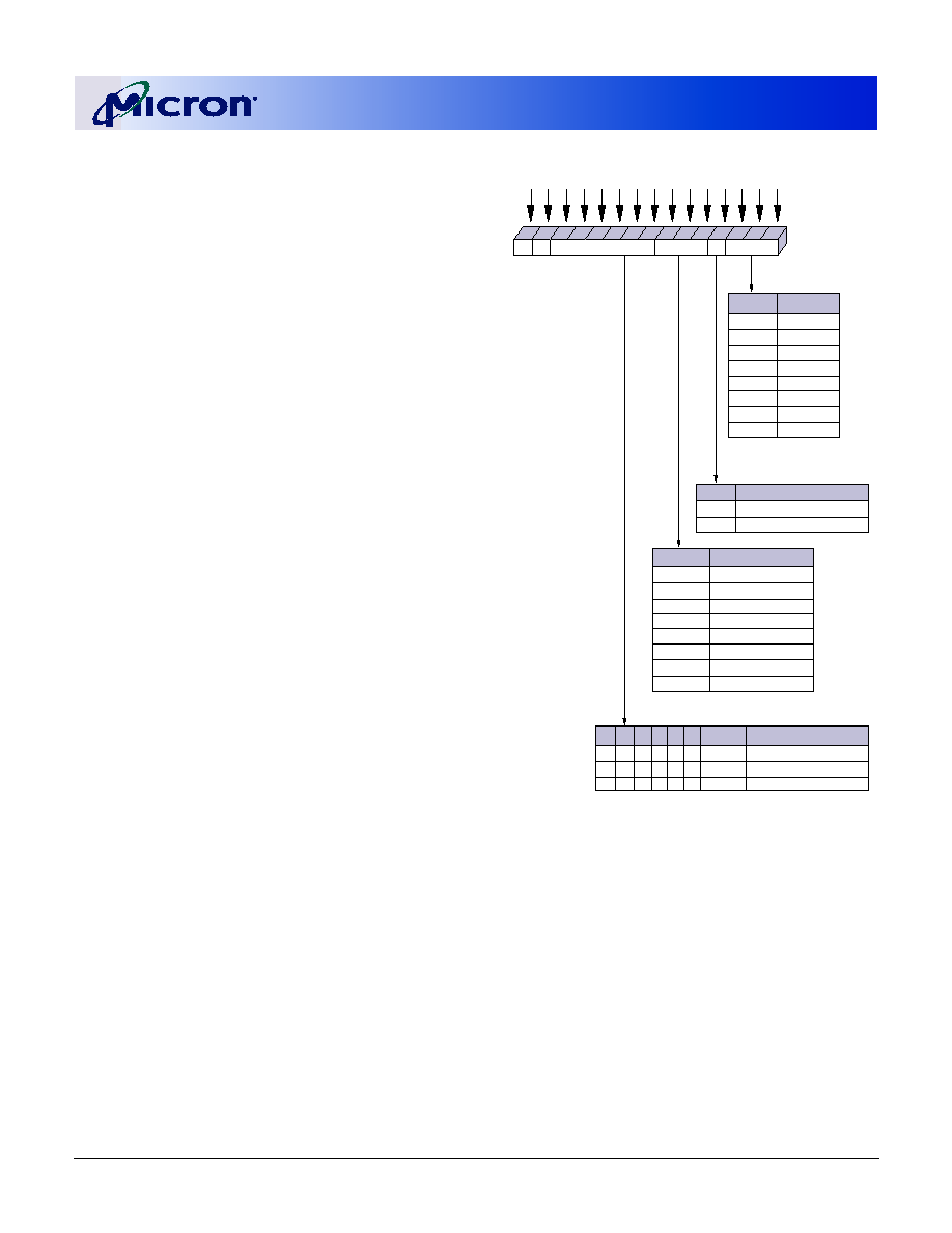
Figure 1: Pin Assignment (Top View)
66-Pin TSOP
256Mb: x4, x8, x16
DDR SDRAM
09005aef8076894f
Micron Technology, Inc., reserves the right to change products or specifications without notice.
256MBDDRx4x8x16_1.fm - Rev. F 6/03 EN
2
©2003 Micron Technology, Inc.
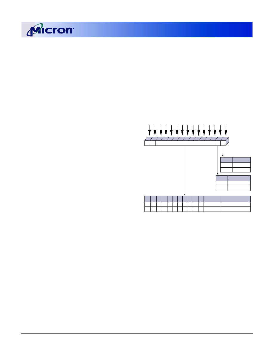
Figure 2: 256Mb DDR SDRAM Part
Numbers
General Description
The 256Mb DDR SDRAM is a high-speed CMOS,
dynamic random-access memory containing
268,435,456 bits. It is internally configured as a quad-
bank DRAM.
The 256Mb DDR SDRAM uses a double-data-rate
architecture to achieve high-speed operation. The
double data rate architecture is essentially a 2n-
prefetch architecture with an interface designed to
transfer two data words per clock cycle at the I/O pins.
A single read or write access for the 256Mb DDR
SDRAM effectively consists of a single 2n-bit wide,
one-clock-cycle data transfer at the internal DRAM
core and two corresponding n-bit wide, one-half-
clock-cycle data transfers at the I/O pins.
A bidirectional data strobe (DQS) is transmitted
externally, along with data, for use in data capture at
the receiver. DQS is a strobe transmitted by the DDR
SDRAM during READs and by the memory controller
during WRITEs. DQS is edge-aligned with data for
READs and center-aligned with data for WRITEs. The
x16 offering has two data strobes, one for the lower
byte and one for the upper byte.
The 256Mb DDR SDRAM operates from a differen-
tial clock (CK and CK#); the crossing of CK going HIGH
and CK# going LOW will be referred to as the positive
edge of CK. Commands (address and control signals)
are registered at every positive edge of CK. Input data
is registered on both edges of DQS, and output data is
referenced to both edges of DQS, as well as to both
edges of CK.
Read and write accesses to the DDR SDRAM are
burst oriented; accesses start at a selected location and
continue for a programmed number of locations in a
programmed sequence. Accesses begin with the regis-
tration of an ACTIVE command, which is then fol-
lowed by a READ or WRITE command. The address
bits registered coincident with the ACTIVE command
are used to select the bank and row to be accessed. The
address bits registered coincident with the READ or
WRITE command are used to select the bank and the
starting column location for the burst access.
The DDR SDRAM provides for programmable READ
or WRITE burst lengths of 2, 4, or 8 locations. An auto
precharge function may be enabled to provide a self-
timed row precharge that is initiated at the end of the
burst access.
As with standard SDR SDRAMs, the pipelined,
multibank architecture of DDR SDRAMs allows for
concurrent operation, thereby effectively providing
high bandwidth by hiding row precharge and activa-
tion time.
An auto refresh mode is provided, along with a
power-saving power-down mode. All inputs are com-
patible with the JEDEC standard for SSTL_2. All full
drive option outputs are SSTL_2, Class II-compatible.
NOTE: 1. The functionality and the timing specifica-
tions discussed in this data sheet are for the
DLL-enabled mode of operation.
2. Throughout the data sheet, the various fig-
ures and text refer to DQs as "DQ." The DQ
term is to be interpreted as any and all DQ
collectively, unless specifically stated other-
wise. Additionally, the x16 is divided into
two bytes, the lower byte and upper byte.
For the lower byte (DQ0 through DQ7) DM
refers to LDM and DQS refers to LDQS. For
the upper byte (DQ8 through DQ15) DM
refers to UDM and DQS refers to UDQS.
3. Complete functionality is described
throughout the document and any page or
diagram may have been simplified to con-
vey a topic and may not be inclusive of all
requirements.
4. Any specific requirement takes precedence
over a general statement.
-
L
H
Special Options
Standard
Low Power
High-Speed Process
Configuration
MT46V
Package
Speed
Special
Options
Temperature
Configuration
64 Meg x 4
32 Meg x 8
16 Meg x 16
64M4
32M8
16M16
Package
400-mil TSOP
400-mil TSOP (lead-free)
16x9 FBGA
16x9 FBGA (lead-free)
14x9 FBGA
14x9 FBGA (lead-free)
TG
P
FJ
BJ
FG
BG
Speed Grade
tCK = 6ns, CL = 2.5
tCK = 6ns, CL = 2.5
tCK = 6ns, CL = 2.5
tCK = 7.5ns, CL = 2
tCK = 7.5ns, CL = 2
tCK = 7.5ns, CL = 2.5
-6
-6T
-6R
-75E
-75Z
-75
I T
Operating Temp
Standard
Industrial Temp
Example Part Number: MT46V16M16TG-75Z H

256Mb: x4, x8, x16
DDR SDRAM
09005aef8076894f
Micron Technology, Inc., reserves the right to change products or specifications without notice.
256MBDDRx4x8x16TOC.fm - Rev. F 6/03 EN
3
©2003 Micron Technology, Inc.
Table of Contents
Features . . . . . . . . . . . . . . . . . . . . . . . . . . . . . . . . . . . . . . . . . . . . . . . . . . . . . . . . . . . . . . . . . . . . . . . . . . . . . . . . . . . . . . . . . . . . . .1
General Description . . . . . . . . . . . . . . . . . . . . . . . . . . . . . . . . . . . . . . . . . . . . . . . . . . . . . . . . . . . . . . . . . . . . . . . . . . . . . . . . . . .2
Functional Description . . . . . . . . . . . . . . . . . . . . . . . . . . . . . . . . . . . . . . . . . . . . . . . . . . . . . . . . . . . . . . . . . . . . . . . . . . . . . . .12
Initialization . . . . . . . . . . . . . . . . . . . . . . . . . . . . . . . . . . . . . . . . . . . . . . . . . . . . . . . . . . . . . . . . . . . . . . . . . . . . . . . . . . . . . .12
Register Definition . . . . . . . . . . . . . . . . . . . . . . . . . . . . . . . . . . . . . . . . . . . . . . . . . . . . . . . . . . . . . . . . . . . . . . . . . . . . . . . . .12
Mode Register. . . . . . . . . . . . . . . . . . . . . . . . . . . . . . . . . . . . . . . . . . . . . . . . . . . . . . . . . . . . . . . . . . . . . . . . . . . . . . . . . . .12
Burst Length . . . . . . . . . . . . . . . . . . . . . . . . . . . . . . . . . . . . . . . . . . . . . . . . . . . . . . . . . . . . . . . . . . . . . . . . . . . . . . . . . . . .13
Burst Type . . . . . . . . . . . . . . . . . . . . . . . . . . . . . . . . . . . . . . . . . . . . . . . . . . . . . . . . . . . . . . . . . . . . . . . . . . . . . . . . . . . . . .13
Read Latency . . . . . . . . . . . . . . . . . . . . . . . . . . . . . . . . . . . . . . . . . . . . . . . . . . . . . . . . . . . . . . . . . . . . . . . . . . . . . . . . . . .14
Operating Mode. . . . . . . . . . . . . . . . . . . . . . . . . . . . . . . . . . . . . . . . . . . . . . . . . . . . . . . . . . . . . . . . . . . . . . . . . . . . . . . . .14
Extended Mode Register . . . . . . . . . . . . . . . . . . . . . . . . . . . . . . . . . . . . . . . . . . . . . . . . . . . . . . . . . . . . . . . . . . . . . . . . . . . .15
Output Drive Strength . . . . . . . . . . . . . . . . . . . . . . . . . . . . . . . . . . . . . . . . . . . . . . . . . . . . . . . . . . . . . . . . . . . . . . . . . . .15
DLL Enable/Disable . . . . . . . . . . . . . . . . . . . . . . . . . . . . . . . . . . . . . . . . . . . . . . . . . . . . . . . . . . . . . . . . . . . . . . . . . . . . .15
Commands . . . . . . . . . . . . . . . . . . . . . . . . . . . . . . . . . . . . . . . . . . . . . . . . . . . . . . . . . . . . . . . . . . . . . . . . . . . . . . . . . . . . . . . . . .16
DESELECT . . . . . . . . . . . . . . . . . . . . . . . . . . . . . . . . . . . . . . . . . . . . . . . . . . . . . . . . . . . . . . . . . . . . . . . . . . . . . . . . . . . . . . . .17
NO OPERATION (NOP). . . . . . . . . . . . . . . . . . . . . . . . . . . . . . . . . . . . . . . . . . . . . . . . . . . . . . . . . . . . . . . . . . . . . . . . . . . . .17
LOAD MODE REGISTER . . . . . . . . . . . . . . . . . . . . . . . . . . . . . . . . . . . . . . . . . . . . . . . . . . . . . . . . . . . . . . . . . . . . . . . . . . . .17
ACTIVE . . . . . . . . . . . . . . . . . . . . . . . . . . . . . . . . . . . . . . . . . . . . . . . . . . . . . . . . . . . . . . . . . . . . . . . . . . . . . . . . . . . . . . . . . . .17
READ . . . . . . . . . . . . . . . . . . . . . . . . . . . . . . . . . . . . . . . . . . . . . . . . . . . . . . . . . . . . . . . . . . . . . . . . . . . . . . . . . . . . . . . . . . . . .17
WRITE . . . . . . . . . . . . . . . . . . . . . . . . . . . . . . . . . . . . . . . . . . . . . . . . . . . . . . . . . . . . . . . . . . . . . . . . . . . . . . . . . . . . . . . . . . . .17
PRECHARGE . . . . . . . . . . . . . . . . . . . . . . . . . . . . . . . . . . . . . . . . . . . . . . . . . . . . . . . . . . . . . . . . . . . . . . . . . . . . . . . . . . . . . .17
Auto Precharge . . . . . . . . . . . . . . . . . . . . . . . . . . . . . . . . . . . . . . . . . . . . . . . . . . . . . . . . . . . . . . . . . . . . . . . . . . . . . . . . . . . .17
BURST TERMINATE . . . . . . . . . . . . . . . . . . . . . . . . . . . . . . . . . . . . . . . . . . . . . . . . . . . . . . . . . . . . . . . . . . . . . . . . . . . . . . .18
AUTO REFRESH . . . . . . . . . . . . . . . . . . . . . . . . . . . . . . . . . . . . . . . . . . . . . . . . . . . . . . . . . . . . . . . . . . . . . . . . . . . . . . . . . . .18
SELF REFRESH . . . . . . . . . . . . . . . . . . . . . . . . . . . . . . . . . . . . . . . . . . . . . . . . . . . . . . . . . . . . . . . . . . . . . . . . . . . . . . . . . . . .18
Operations . . . . . . . . . . . . . . . . . . . . . . . . . . . . . . . . . . . . . . . . . . . . . . . . . . . . . . . . . . . . . . . . . . . . . . . . . . . . . . . . . . . . . . . . . .19
Bank/Row Activation. . . . . . . . . . . . . . . . . . . . . . . . . . . . . . . . . . . . . . . . . . . . . . . . . . . . . . . . . . . . . . . . . . . . . . . . . . . . . . .19
READs . . . . . . . . . . . . . . . . . . . . . . . . . . . . . . . . . . . . . . . . . . . . . . . . . . . . . . . . . . . . . . . . . . . . . . . . . . . . . . . . . . . . . . . . . . . .20
WRITEs . . . . . . . . . . . . . . . . . . . . . . . . . . . . . . . . . . . . . . . . . . . . . . . . . . . . . . . . . . . . . . . . . . . . . . . . . . . . . . . . . . . . . . . . . . .29
PRECHARGE . . . . . . . . . . . . . . . . . . . . . . . . . . . . . . . . . . . . . . . . . . . . . . . . . . . . . . . . . . . . . . . . . . . . . . . . . . . . . . . . . . . . . .40
Power-Down (CKE Not Active) . . . . . . . . . . . . . . . . . . . . . . . . . . . . . . . . . . . . . . . . . . . . . . . . . . . . . . . . . . . . . . . . . . . . . .40
Absolute Maximum Ratings . . . . . . . . . . . . . . . . . . . . . . . . . . . . . . . . . . . . . . . . . . . . . . . . . . . . . . . . . . . . . . . . . . . . . . . . . . .46
Notes . . . . . . . . . . . . . . . . . . . . . . . . . . . . . . . . . . . . . . . . . . . . . . . . . . . . . . . . . . . . . . . . . . . . . . . . . . . . . . . . . . . . . . . . . . . . . . .59
Data Sheet Designation . . . . . . . . . . . . . . . . . . . . . . . . . . . . . . . . . . . . . . . . . . . . . . . . . . . . . . . . . . . . . . . . . . . . . . . . . . . . . . .80

256Mb: x4, x8, x16
DDR SDRAM
09005aef8076894f
Micron Technology, Inc., reserves the right to change products or specifications without notice.
256MBDDRx4x8x16LOF.fm - Rev. F 6/03 EN
4
©2003 Micron Technology, Inc.
List of Figures
Figure 1:
Pin Assignment (Top View) 66-Pin TSOP . . . . . . . . . . . . . . . . . . . . . . . . . . . . . . . . . . . . . . . . . . . . . . . . . . . .1
Figure 2:
256Mb DDR SDRAM Part Numbers . . . . . . . . . . . . . . . . . . . . . . . . . . . . . . . . . . . . . . . . . . . . . . . . . . . . . . . . .2
Figure 3:
Functional Block Diagram: 64 Meg x 4. . . . . . . . . . . . . . . . . . . . . . . . . . . . . . . . . . . . . . . . . . . . . . . . . . . . . . .6
Figure 4:
Functional Block Diagram: 32 Meg x 8. . . . . . . . . . . . . . . . . . . . . . . . . . . . . . . . . . . . . . . . . . . . . . . . . . . . . . .7
Figure 5:
Functional Block Diagram: 16 Meg x 16. . . . . . . . . . . . . . . . . . . . . . . . . . . . . . . . . . . . . . . . . . . . . . . . . . . . . .8
Figure 6:
60-Ball FBGA Ball Assignment (Top View) . . . . . . . . . . . . . . . . . . . . . . . . . . . . . . . . . . . . . . . . . . . . . . . . . .11
Figure 7:
Mode Register Definition . . . . . . . . . . . . . . . . . . . . . . . . . . . . . . . . . . . . . . . . . . . . . . . . . . . . . . . . . . . . . . . . .13
Figure 8:
CAS Latency . . . . . . . . . . . . . . . . . . . . . . . . . . . . . . . . . . . . . . . . . . . . . . . . . . . . . . . . . . . . . . . . . . . . . . . . . . . .14
Figure 9:
Extended Mode Register Definition . . . . . . . . . . . . . . . . . . . . . . . . . . . . . . . . . . . . . . . . . . . . . . . . . . . . . . . .15
Figure 10:
Activating a Specific Row in a Specific Bank . . . . . . . . . . . . . . . . . . . . . . . . . . . . . . . . . . . . . . . . . . . . . . . .19
Figure 11:
Example: Meeting
t
RCD (
t
RRD) MIN When 2 <
t
RCD (
t
RRD) MIN/
t
CK
£ 3 . . . . . . . . . . . . . . . . . . . . . .19
Figure 12:
READ Command. . . . . . . . . . . . . . . . . . . . . . . . . . . . . . . . . . . . . . . . . . . . . . . . . . . . . . . . . . . . . . . . . . . . . . . . .21
Figure 13:
READ Burst. . . . . . . . . . . . . . . . . . . . . . . . . . . . . . . . . . . . . . . . . . . . . . . . . . . . . . . . . . . . . . . . . . . . . . . . . . . . . .22
Figure 14:
Consecutive READ Bursts . . . . . . . . . . . . . . . . . . . . . . . . . . . . . . . . . . . . . . . . . . . . . . . . . . . . . . . . . . . . . . . . .23
Figure 15:
Nonconsecutive READ Bursts . . . . . . . . . . . . . . . . . . . . . . . . . . . . . . . . . . . . . . . . . . . . . . . . . . . . . . . . . . . . .24
Figure 16:
Random READ Accesses . . . . . . . . . . . . . . . . . . . . . . . . . . . . . . . . . . . . . . . . . . . . . . . . . . . . . . . . . . . . . . . . . .25
Figure 17:
Terminating a READ Burst . . . . . . . . . . . . . . . . . . . . . . . . . . . . . . . . . . . . . . . . . . . . . . . . . . . . . . . . . . . . . . . .26
Figure 18:
READ to WRITE . . . . . . . . . . . . . . . . . . . . . . . . . . . . . . . . . . . . . . . . . . . . . . . . . . . . . . . . . . . . . . . . . . . . . . . . . .27
Figure 19:
READ to PRECHARGE . . . . . . . . . . . . . . . . . . . . . . . . . . . . . . . . . . . . . . . . . . . . . . . . . . . . . . . . . . . . . . . . . . . .28
Figure 20:
WRITE Command . . . . . . . . . . . . . . . . . . . . . . . . . . . . . . . . . . . . . . . . . . . . . . . . . . . . . . . . . . . . . . . . . . . . . . .29
Figure 21:
WRITE Burst. . . . . . . . . . . . . . . . . . . . . . . . . . . . . . . . . . . . . . . . . . . . . . . . . . . . . . . . . . . . . . . . . . . . . . . . . . . . .30
Figure 22:
Consecutive WRITE to WRITE . . . . . . . . . . . . . . . . . . . . . . . . . . . . . . . . . . . . . . . . . . . . . . . . . . . . . . . . . . . . .31
Figure 23:
Nonconsecutive WRITE to WRITE . . . . . . . . . . . . . . . . . . . . . . . . . . . . . . . . . . . . . . . . . . . . . . . . . . . . . . . . .32
Figure 24:
Random WRITE Cycles . . . . . . . . . . . . . . . . . . . . . . . . . . . . . . . . . . . . . . . . . . . . . . . . . . . . . . . . . . . . . . . . . . .33
Figure 25:
WRITE to READ - Uninterrupting . . . . . . . . . . . . . . . . . . . . . . . . . . . . . . . . . . . . . . . . . . . . . . . . . . . . . . . . . .34
Figure 26:
WRITE to READ ≠ Interrupting . . . . . . . . . . . . . . . . . . . . . . . . . . . . . . . . . . . . . . . . . . . . . . . . . . . . . . . . . . . .35
Figure 27:
WRITE to READ ≠ Odd Number of Data, Interrupting . . . . . . . . . . . . . . . . . . . . . . . . . . . . . . . . . . . . . . . .36
Figure 28:
WRITE to PRECHARGE - Uninterrupting . . . . . . . . . . . . . . . . . . . . . . . . . . . . . . . . . . . . . . . . . . . . . . . . . . .37
Figure 29:
WRITE to PRECHARGE ≠ Interrupting . . . . . . . . . . . . . . . . . . . . . . . . . . . . . . . . . . . . . . . . . . . . . . . . . . . . . .38
Figure 30:
WRITE to PRECHARGE ≠ Odd Number of Data ≠ Interrupting . . . . . . . . . . . . . . . . . . . . . . . . . . . . . . . .39
Figure 31:
PRECHARGE Command . . . . . . . . . . . . . . . . . . . . . . . . . . . . . . . . . . . . . . . . . . . . . . . . . . . . . . . . . . . . . . . . .40
Figure 32:
Power-Down . . . . . . . . . . . . . . . . . . . . . . . . . . . . . . . . . . . . . . . . . . . . . . . . . . . . . . . . . . . . . . . . . . . . . . . . . . . .41
Figure 33:
Input Voltage Waveform . . . . . . . . . . . . . . . . . . . . . . . . . . . . . . . . . . . . . . . . . . . . . . . . . . . . . . . . . . . . . . . . . .47
Figure 34:
SSTL_2 Clock Input . . . . . . . . . . . . . . . . . . . . . . . . . . . . . . . . . . . . . . . . . . . . . . . . . . . . . . . . . . . . . . . . . . . . . .48
Figure 35:
Derating Data Valid Window (
t
QH -
t
DQSQ) . . . . . . . . . . . . . . . . . . . . . . . . . . . . . . . . . . . . . . . . . . . . . . . .60
Figure 36:
Full Drive Pull-Down Characteristics . . . . . . . . . . . . . . . . . . . . . . . . . . . . . . . . . . . . . . . . . . . . . . . . . . . . . .61
Figure 37:
Full Drive Pull-Up Characteristics . . . . . . . . . . . . . . . . . . . . . . . . . . . . . . . . . . . . . . . . . . . . . . . . . . . . . . . . .61
Figure 38:
Reduced Drive Pull-Down Characteristics . . . . . . . . . . . . . . . . . . . . . . . . . . . . . . . . . . . . . . . . . . . . . . . . . .62
Figure 39:
Reduced Drive Pull-Up Characteristics . . . . . . . . . . . . . . . . . . . . . . . . . . . . . . . . . . . . . . . . . . . . . . . . . . . .62
Figure 40:
x4, x8 Data Output Timing ≠
t
DQSQ,
t
QH, and Data Valid Window . . . . . . . . . . . . . . . . . . . . . . . . . . . .65
Figure 41:
x16 Data Output Timing ≠
t
DQSQ,
t
QH, and Data Valid Window . . . . . . . . . . . . . . . . . . . . . . . . . . . . . .66
Figure 42:
Data Output Timing ≠
t
AC and
t
DQSCK . . . . . . . . . . . . . . . . . . . . . . . . . . . . . . . . . . . . . . . . . . . . . . . . . . . .67
Figure 43:
Data Input Timing . . . . . . . . . . . . . . . . . . . . . . . . . . . . . . . . . . . . . . . . . . . . . . . . . . . . . . . . . . . . . . . . . . . . . . .68
Figure 44:
Initialize and Load Mode Registers. . . . . . . . . . . . . . . . . . . . . . . . . . . . . . . . . . . . . . . . . . . . . . . . . . . . . . . . .69
Figure 45:
Power-Down Mode . . . . . . . . . . . . . . . . . . . . . . . . . . . . . . . . . . . . . . . . . . . . . . . . . . . . . . . . . . . . . . . . . . . . . .70
Figure 46:
Auto Refresh Mode . . . . . . . . . . . . . . . . . . . . . . . . . . . . . . . . . . . . . . . . . . . . . . . . . . . . . . . . . . . . . . . . . . . . . . .71
Figure 47:
Self Refresh Mode . . . . . . . . . . . . . . . . . . . . . . . . . . . . . . . . . . . . . . . . . . . . . . . . . . . . . . . . . . . . . . . . . . . . . . . .72
Figure 48:
Bank Read - Without Auto Precharge . . . . . . . . . . . . . . . . . . . . . . . . . . . . . . . . . . . . . . . . . . . . . . . . . . . . . . .73
Figure 49:
Bank Read - With Auto Precharge . . . . . . . . . . . . . . . . . . . . . . . . . . . . . . . . . . . . . . . . . . . . . . . . . . . . . . . . . .74
Figure 50:
Bank Write - Without Auto Precharge . . . . . . . . . . . . . . . . . . . . . . . . . . . . . . . . . . . . . . . . . . . . . . . . . . . . . .75
Figure 51:
Bank Write - With Auto Precharge . . . . . . . . . . . . . . . . . . . . . . . . . . . . . . . . . . . . . . . . . . . . . . . . . . . . . . . . .76
Figure 52:
Write ≠ DM Operation . . . . . . . . . . . . . . . . . . . . . . . . . . . . . . . . . . . . . . . . . . . . . . . . . . . . . . . . . . . . . . . . . . . .77
Figure 53:
66-Pin Plastic TSOP (400 mil). . . . . . . . . . . . . . . . . . . . . . . . . . . . . . . . . . . . . . . . . . . . . . . . . . . . . . . . . . . . . .78
Figure 54:
60-Ball FBGA (16 x 9mm) . . . . . . . . . . . . . . . . . . . . . . . . . . . . . . . . . . . . . . . . . . . . . . . . . . . . . . . . . . . . . . . . .79
Figure 55:
60-Ball FBGA (14 x 8mm) . . . . . . . . . . . . . . . . . . . . . . . . . . . . . . . . . . . . . . . . . . . . . . . . . . . . . . . . . . . . . . . . .80

256Mb: x4, x8, x16
DDR SDRAM
09005aef8076894f
Micron Technology, Inc., reserves the right to change products or specifications without notice.
256MBDDRx4x8x16LOT.fm - Rev. F 6/03 EN
5
©2003 Micron Technology, Inc.
List of Tables
Table 1:
Key Timing Parameters . . . . . . . . . . . . . . . . . . . . . . . . . . . . . . . . . . . . . . . . . . . . . . . . . . . . . . . . . . . . . . . . . . . .1
Table 2:
Ball/Pin Descriptions. . . . . . . . . . . . . . . . . . . . . . . . . . . . . . . . . . . . . . . . . . . . . . . . . . . . . . . . . . . . . . . . . . . . . .9
Table 3:
Reserved NC Balls and Pins
1
. . . . . . . . . . . . . . . . . . . . . . . . . . . . . . . . . . . . . . . . . . . . . . . . . . . . . . . . . . . . . .10
Table 4:
Burst Definition. . . . . . . . . . . . . . . . . . . . . . . . . . . . . . . . . . . . . . . . . . . . . . . . . . . . . . . . . . . . . . . . . . . . . . . . . .14
Table 5:
CAS Latency (CL) . . . . . . . . . . . . . . . . . . . . . . . . . . . . . . . . . . . . . . . . . . . . . . . . . . . . . . . . . . . . . . . . . . . . . . . .14
Table 6:
Truth Table ≠ Commands . . . . . . . . . . . . . . . . . . . . . . . . . . . . . . . . . . . . . . . . . . . . . . . . . . . . . . . . . . . . . . . . .16
Table 7:
Truth Table ≠ DM Operation . . . . . . . . . . . . . . . . . . . . . . . . . . . . . . . . . . . . . . . . . . . . . . . . . . . . . . . . . . . . . .16
Table 8:
Truth Table ≠ CKE. . . . . . . . . . . . . . . . . . . . . . . . . . . . . . . . . . . . . . . . . . . . . . . . . . . . . . . . . . . . . . . . . . . . . . . .41
Table 9:
Truth Table ≠ Current State Bank n ≠ Command to Bank n . . . . . . . . . . . . . . . . . . . . . . . . . . . . . . . . . . .42
Table 10:
Truth Table ≠ Current State Bank n≠ Command to Bank m . . . . . . . . . . . . . . . . . . . . . . . . . . . . . . . . . . .44
Table 11:
DC Electrical Characteristics and Operating Conditions. . . . . . . . . . . . . . . . . . . . . . . . . . . . . . . . . . . . . .46
Table 12:
AC Input Operating Conditions. . . . . . . . . . . . . . . . . . . . . . . . . . . . . . . . . . . . . . . . . . . . . . . . . . . . . . . . . . . .46
Table 13:
Clock Input Operating Conditions . . . . . . . . . . . . . . . . . . . . . . . . . . . . . . . . . . . . . . . . . . . . . . . . . . . . . . . . .48
Table 14:
Capacitance (x4, x8 TSOP) . . . . . . . . . . . . . . . . . . . . . . . . . . . . . . . . . . . . . . . . . . . . . . . . . . . . . . . . . . . . . . . .49
Table 15:
Capacitance (x4, x8 FBGA) . . . . . . . . . . . . . . . . . . . . . . . . . . . . . . . . . . . . . . . . . . . . . . . . . . . . . . . . . . . . . . . .49
Table 16:
Capacitance (x16 TSOP) . . . . . . . . . . . . . . . . . . . . . . . . . . . . . . . . . . . . . . . . . . . . . . . . . . . . . . . . . . . . . . . . . .50
Table 17:
Capacitance (x16 FBGA) . . . . . . . . . . . . . . . . . . . . . . . . . . . . . . . . . . . . . . . . . . . . . . . . . . . . . . . . . . . . . . . . . .50
Table 18:
I
DD
Specifications and Conditions (x4, x8; -6/-6R/-6T/-75E) . . . . . . . . . . . . . . . . . . . . . . . . . . . . . . . . . .51
Table 19:
I
DD
Specifications and Conditions (x4, x8; -75Z/-75) . . . . . . . . . . . . . . . . . . . . . . . . . . . . . . . . . . . . . . . . .52
Table 20:
I
DD
Specifications and Conditions (x16; -6/-6R/-6T/-75E) . . . . . . . . . . . . . . . . . . . . . . . . . . . . . . . . . . . .53
Table 21:
I
DD
Specifications and Conditions (x16; -75Z/-75) . . . . . . . . . . . . . . . . . . . . . . . . . . . . . . . . . . . . . . . . . . .54
Table 22:
I
DD
Test Cycle Times . . . . . . . . . . . . . . . . . . . . . . . . . . . . . . . . . . . . . . . . . . . . . . . . . . . . . . . . . . . . . . . . . . . . .55
Table 23:
Electrical Characteristics and Recommended AC Operating Conditions (-6/-6T/-6R/-75E) . . . . . .56
Table 24:
Electrical Characteristics and Recommended AC Operating Conditions (-75Z/-75) . . . . . . . . . . . . .57
Table 25:
Input Slew Rate Derating Values for Addresses and Commands . . . . . . . . . . . . . . . . . . . . . . . . . . . . . . .58
Table 26:
Input Slew Rate Derating Values for DQ, DQS, and DM . . . . . . . . . . . . . . . . . . . . . . . . . . . . . . . . . . . . . .58
Table 27:
Normal Output Drive Characteristics . . . . . . . . . . . . . . . . . . . . . . . . . . . . . . . . . . . . . . . . . . . . . . . . . . . . . .63
Table 28:
Reduced Output Drive Characteristics . . . . . . . . . . . . . . . . . . . . . . . . . . . . . . . . . . . . . . . . . . . . . . . . . . . . .64

256Mb: x4, x8, x16
DDR SDRAM
09005aef8076894f
Micron Technology, Inc., reserves the right to change products or specifications without notice.
256MBDDRx4x8x16_2.fm - Rev. F 6/03 EN
6
©2003 Micron Technology, Inc.
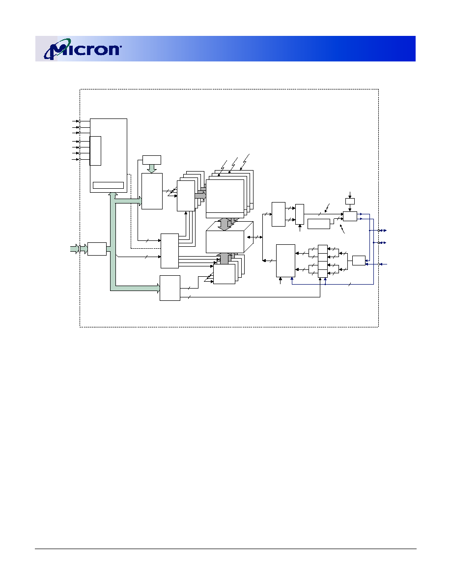
Figure 3: Functional Block Diagram: 64 Meg x 4
13
RAS#
CAS#
ROW-
ADDRESS
MUX
CK
CS#
WE#
CK#
CONTROL
LOGIC
COLUMN-
ADDRESS
COUNTER/
LATCH
MODE REGISTERS
11
COMMAND
DECODE
A0-A12,
BA0, BA1
CKE
13
ADDRESS
REGISTER
15
1024
(x8)
8192
I/O GATING
DM MASK LOGIC
COLUMN
DECODER
BANK0
MEMORY
ARRAY
(8,192 x 1,024 x 8)
BANK0
ROW-
ADDRESS
LATCH
&
DECODER
8192
SENSE AMPLIFIERS
BANK
CONTROL
LOGIC
15
BANK1
BANK2
BANK3
13
10
1
2
2
REFRESH
COUNTER
4
4
4
1
INPUT
REGISTERS
1
1
1
1
RCVRS
1
8
8
2
8
clk
out
DATA
DQS
MASK
DATA
CK
CK
COL0
clk
in
DRVRS
DLL
MUX
DQS
GENERATOR
4
4
4
4
4
8
DQ0≠
DQ3
DQS
DM
1
READ
LATCH
WRITE
FIFO
&
DRIVERS
COL0

256Mb: x4, x8, x16
DDR SDRAM
09005aef8076894f
Micron Technology, Inc., reserves the right to change products or specifications without notice.
256MBDDRx4x8x16_2.fm - Rev. F 6/03 EN
7
©2003 Micron Technology, Inc.
Figure 4: Functional Block Diagram: 32 Meg x 8
13
RAS#
CAS#
ROW-
ADDRESS
MUX
CK
CS#
WE#
CK#
CONTROL
LOGIC
COLUMN-
ADDRESS
COUNTER/
LATCH
MODE REGISTERS
10
COMMAND
DECODE
A0-A12,
BA0, BA1
CKE
13
ADDRESS
REGISTER
15
512
(x16)
8192
I/O GATING
DM MASK LOGIC
COLUMN
DECODER
BANK0
MEMORY
ARRAY
(8192 x 512 x 16)
BANK0
ROW-
ADDRESS
LATCH
&
DECODER
8192
SENSE AMPLIFIERS
BANK
CONTROL
LOGIC
15
BANK1
BANK2
BANK3
13
9
2
2
REFRESH
COUNTER
8
8
8
1
INPUT
REGISTERS
1
1
1
1
RCVRS
1
16
16
2
16
clk
out
DATA
DQS
MASK
DATA
CK
CK
clk
in
DRVRS
DLL
MUX
DQS
GENERATOR
8
8
8
8
8
16
DQ0≠
DQ7
DQS
1
READ
LATCH
WRITE
FIFO
&
DRIVERS
1
COL0
COL0
DM
256Mb: x4, x8, x16
DDR SDRAM
09005aef8076894f
Micron Technology, Inc., reserves the right to change products or specifications without notice.
256MBDDRx4x8x16_2.fm - Rev. F 6/03 EN
8
©2003 Micron Technology, Inc.
Figure 5: Functional Block Diagram: 16 Meg x 16
13
RAS#
CAS#
ROW-
ADDRESS
MUX
CK
CS#
WE#
CK#
CONTROL
LOGIC
COLUMN-
ADDRESS
COUNTER/
LATCH
MODE REGISTERS
9
COMMAND
DECODE
A0-A12,
BA0, BA1
CKE
13
ADDRESS
REGISTER
15
256
(x32)
8192
I/O GATING
DM MASK LOGIC
COLUMN
DECODER
BANK0
MEMORY
ARRAY
(8,192 x 256 x 32)
BANK0
ROW-
ADDRESS
LATCH
&
DECODER
8192
SENSE AMPLIFIERS
BANK
CONTROL
LOGIC
15
BANK1
BANK2
BANK3
13
8
2
2
REFRESH
COUNTER
16
16
16
2
INPUT
REGISTERS
2
2
2
2
RCVRS
2
32
32
4
32
clk
out
DATA
DQS
MASK
DATA
CK
C K
clk
in
DRVRS
DLL
MUX
DQS
GENERATOR
16
16
16
16
16
32
DQ0 -
DQ15
LDQS
UDQS
2
READ
LATCH
WRITE
FIFO
&
DRIVERS
1
COL0
COL0
LDM,
UDM
256Mb: x4, x8, x16
DDR SDRAM
09005aef8076894f
Micron Technology, Inc., reserves the right to change products or specifications without notice.
256MBDDRx4x8x16_2.fm - Rev. F 6/03 EN
9
©2003 Micron Technology, Inc.
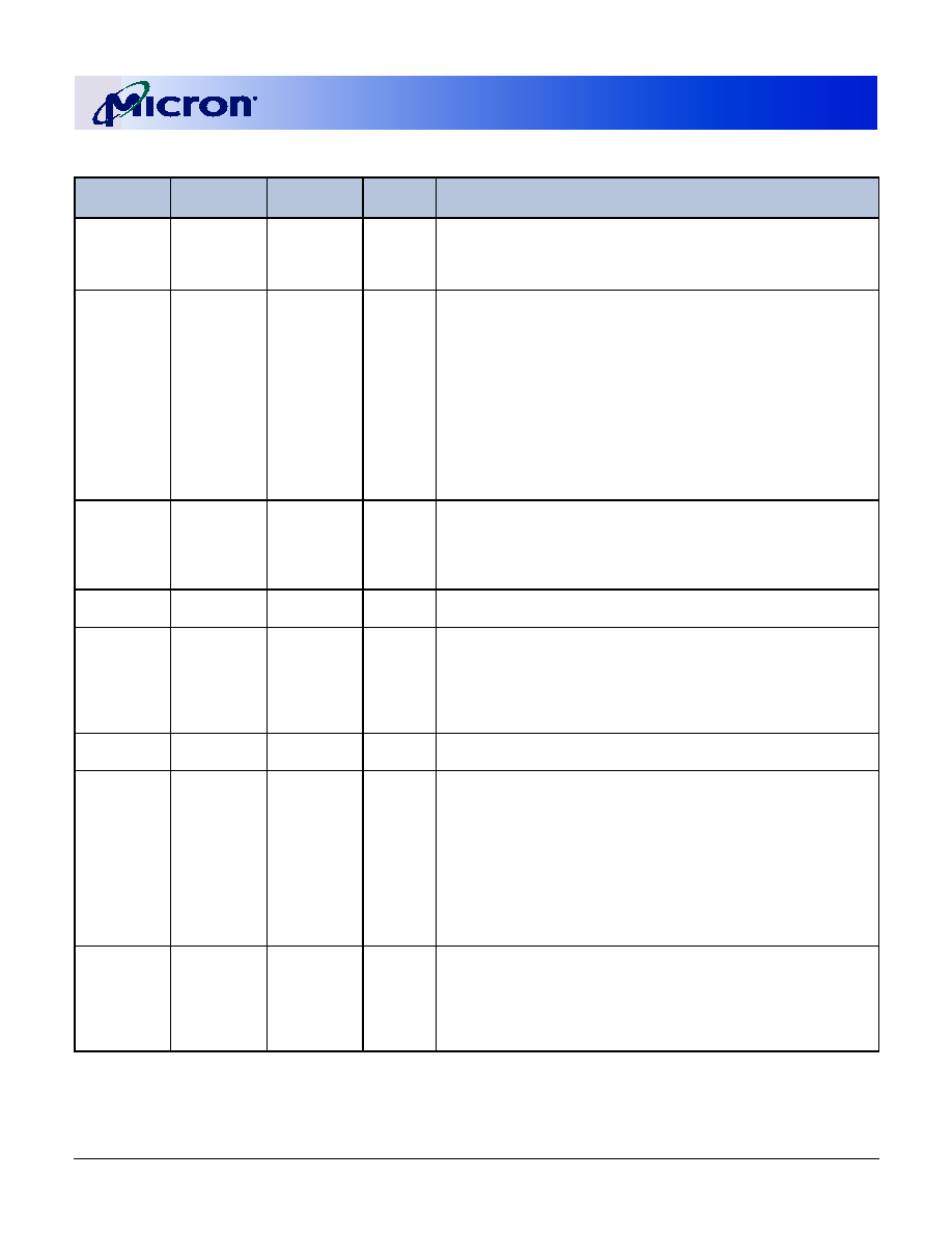
Table 2:
Ball/Pin Descriptions
FBGA
NUMBERS
TSOP
NUMBERS
SYMBOL
TYPE
DESCRIPTION
G2, G3
45, 46
CK, CK#
Input
Clock: CK and CK# are differential clock inputs. All address and
control input signals are sampled on the crossing of the positive
edge of CK and the negative edge of CK#. Output data (DQ and
DQS) is referenced to the crossings of CK and CK#.
H3
44
CKE
Input
Clock Enable: CKE HIGH activates and CKE LOW deactivates the
internal clock, input buffers, and output drivers. Taking CKE LOW
provides PRECHARGE POWER-DOWN and SELF REFRESH operations
(all banks idle) or ACTIVE POWER-DOWN (row ACTIVE in any bank).
CKE is synchronous for POWER-DOWN entry and exit and for SELF
REFRESH entry. CKE is asynchronous for SELF REFRESH exit and for
disabling the outputs. CKE must be maintained HIGH throughout
read and write accesses. Input buffers (excluding CK, CK#, and CKE)
are disabled during POWER- DOWN. Input buffers (excluding CKE)
are disabled during SELF REFRESH. CKE is an SSTL_2 input but will
detect an LVCMOS
LOW level after V
DD
is applied and until CKE is
first brought
HIGH, after which it becomes an SSTL_2 input only.
H8
24
CS#
Input
Chip Select: CS# enables (registered LOW) and disables (registered
HIGH) the command decoder. All commands are masked when CS#
is registered HIGH. CS# provides for external bank selection on
systems with multiple banks. CS# is considered part of the
command code.
H7, G8, G7
23, 22, 21
RAS#, CAS#,
WE#
Input
Command Inputs: RAS#, CAS#, and WE# (along with CS#) define
the command being entered.
3F
47
DM
Input
Input Data Mask: DM is an input mask signal for write data. Input
data is masked when DM is sampled HIGH along with that input
data during a WRITE access. DM is sampled on both edges of DQS.
Although DM pins are input-only, the DM loading is designed to
match that of DQ and DQS pins. For the x16, LDM is DM for DQ0≠
DQ7 and UDM is DM for DQ8≠DQ15. Pin 20 is a NC on x4 and x8.
F7, 3F
20, 47
LDM, UDM
J8, J7
26, 27
BA0, BA1
Input
Bank Address Inputs: BA0 and BA1 define to which bank an
ACTIVE, READ, WRITE, or PRECHARGE command is being applied.
K7, L8, L7,
M8, M2, L3,
L2, K3, K2, J3,
K8,
J2, H2
29, 30, 31, 32,
35, 36, 37, 38,
39, 40, 28
41, 42
A0, A1, A2,
A3, A4, A5,
A6, A7, A8,
A9, A10, A11,
A12
Input
Address Inputs: Provide the row address for ACTIVE commands, and
the column address and auto precharge bit (A10) for READ/WRITE
commands, to select one location out of the memory array in the
respective bank. A10 sampled during a PRECHARGE command
determines whether the PRECHARGE applies to one bank (A10
LOW, bank selected by BA0, BA1) or all banks (A10 HIGH). The
address inputs also provide the op-code during a MODE REGISTER
SET command. BA0 and BA1 define which mode register (mode
register or extended mode register) is loaded during the LOAD
MODE REGISTER command.
A8, B9, B7,
C9, C7, D9,
D7, E9, E1,
D3, D1, C3,
C1, B3, B1, A2
2, 4, 5,
7, 8, 10,
11, 13, 54, 56,
57, 59, 60, 62,
63,
65
DQ0≠DQ2
DQ3≠DQ5
DQ6≠DQ8
DQ9≠DQ11
DQ12≠DQ14
DQ15
I/O
Data Input/Output: Data bus for x16.
(DQ4≠DQ15 are NC for the x4)
(DQ8≠DQ16 are NC for the x8)

256Mb: x4, x8, x16
DDR SDRAM
09005aef8076894f
Micron Technology, Inc., reserves the right to change products or specifications without notice.
256MBDDRx4x8x16_2.fm - Rev. F 6/03 EN
10
©2003 Micron Technology, Inc.
NOTE:
1. NC pins not listed may also be reserved for other uses now or in the future. This table simply defines specific NC pins
deemed to be of importance.
A8, B7, C7,
D7, D3, C3,
B3, A2
2, 5, 8,
11, 56, 59, 62,
65
DQ0≠DQ2
DQ3≠DQ5
DQ6, DQ7
I/O
Data Input/Output: Data bus for x8.
(DQ4≠DQ7 are NC for the x4)
B7, D7, D3,
B3
5, 11, 56,
62
DQ0≠DQ2
DQ3
I/O
Data Input/Output: Data bus for x4.
E3
E7
E3
51
16
51
DQS
LDQS
UDQS
I/O
Data Strobe: Output with read data, input with write data. DQS is
edge-aligned with read data, centered in write data. It is used to
capture data. For the x16, LDQS is DQS for DQ0≠DQ7 and UDQS is
DQS for DQ8≠DQ15. Pin 16 (E7) is NC on x4 and x8.
14, 17, 25, 43,
53
NC
≠
No Connect: These pins should be left unconnected.
F9
19, 50
DNU
≠
Do Not Use: Must float to minimize noise on V
REF
.
B2, D2, C8,
E8, A9
3, 9, 15, 55,
61
V
DD
Q
Supply
DQ Power Supply: +2.5V Ī0.2V. Isolated on the die for improved
noise immunity.
A1, C2, E2,
B8, D8
6, 12, 52, 58,
64
V
SS
Q
Supply
DQ Ground: Isolated on the die for improved noise immunity.
F8, M7, A7
1, 18, 33
V
DD
Supply
Power Supply: +2.5V Ī0.2V.
A3, F2, M3
34, 48, 66
V
SS
Supply
Ground.
F1
49
V
REF
Supply
SSTL_2 reference voltage.
Table 2:
Ball/Pin Descriptions (Continued)
FBGA
NUMBERS
TSOP
NUMBERS
SYMBOL
TYPE
DESCRIPTION
Table 3:
Reserved NC Balls and Pins
1
FBGA
NUMBERS
TSOP
NUMBERS
SYMBOL
TYPE
DESCRIPTION
F9
17
A13
I
Address input A13 for 1Gb devices. DNU for FBGA.
256Mb: x4, x8, x16
DDR SDRAM
09005aef8076894f
Micron Technology, Inc., reserves the right to change products or specifications without notice.
256MBDDRx4x8x16_2.fm - Rev. F 6/03 EN
11
©2003 Micron Technology, Inc.
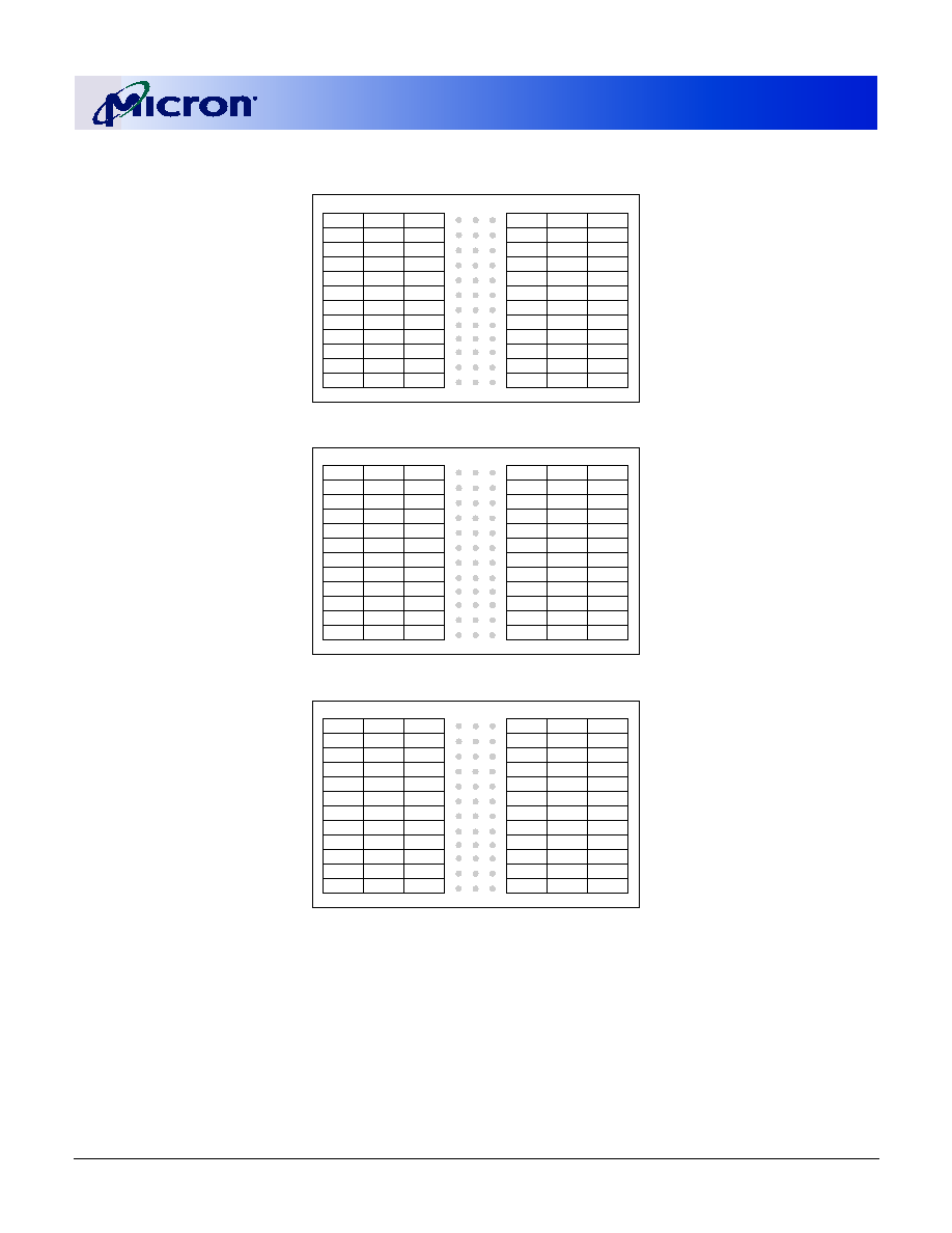
Figure 6: 60-Ball FBGA Ball Assignment (Top View)
V
SS
Q
DQ14
DQ12
DQ10
DQ8
V
REF
DQ15
V
DD
Q
V
SS
Q
V
DD
Q
V
SS
Q
V
SS
CK
A12
A11
A8
A6
A4
V
SS
DQ13
DQ11
DQ9
UDQS
UDM
CK#
CKE
A9
A7
A5
V
SS
V
DD
DQ2
DQ4
DQ6
LDQS
LDM
WE#
RAS#
BA1
A0
A2
V
DD
DQ0
V
SS
Q
V
DD
Q
V
SS
Q
V
DD
Q
V
DD
CAS#
CS#
BA0
A10
A1
A3
V
DD
Q
DQ1
DQ3
DQ5
DQ7
DNU
x16 (Top View)
V
SS
Q
NC
NC
NC
NC
V
REF
NC
V
DD
Q
V
SS
Q
V
DD
Q
V
SS
Q
V
SS
CK
A12
A11
A8
A6
A4
V
SS
DQ3
NC
DQ2
DQS
DM
CK#
CKE
A9
A7
A5
V
SS
V
DD
DQ0
NC
DQ1
NC
NC
WE#
RAS#
BA1
A0
A2
V
DD
NC
V
SS
Q
V
DD
Q
V
SS
Q
V
DD
Q
V
DD
CAS#
CS#
BA0
A10
A1
A3
V
DD
Q
NC
NC
NC
NC
DNU
x4 (Top View)
V
SS
Q
NC
NC
NC
NC
V
REF
DQ7
V
DD
Q
V
SS
Q
V
DD
Q
V
SS
Q
V
SS
CK
A12
A11
A8
A6
A4
V
SS
DQ6
DQ5
DQ4
DQS
DM
CK#
CKE
A9
A7
A5
V
SS
V
DD
DQ1
DQ2
DQ3
NC
NC
WE#
RAS#
BA1
A0
A2
V
DD
DQ0
V
SS
Q
V
DD
Q
V
SS
Q
V
DD
Q
V
DD
CAS#
CS#
BA0
A10
A1
A3
V
DD
Q
NC
NC
NC
NC
DNU
x8 (Top View)
A
1
2
3
4
5
6
7
8
9
B
C
D
E
F
G
H
J
K
L
M
A
1
2
3
4
5
6
7
8
9
B
C
D
E
F
G
H
J
K
L
M
A
1
2
3
4
5
6
7
8
9
B
C
D
E
F
G
H
J
K
L
M

256Mb: x4, x8, x16
DDR SDRAM
09005aef8076894f
Micron Technology, Inc., reserves the right to change products or specifications without notice.
256MBDDRx4x8x16_2.fm - Rev. F 6/03 EN
12
©2003 Micron Technology, Inc.
Functional Description
The 256Mb DDR SDRAM is a high-speed CMOS,
dynamic random-access memory containing
268,435,456 bits. The 256Mb DDR SDRAM is internally
configured as a quad-bank DRAM.
The 256Mb DDR SDRAM uses a double data rate
architecture to achieve high-speed operation. The
double data rate architecture is essentially a 2n-
prefetch architecture, with an interface designed to
transfer two data words per clock cycle at the I/O pins.
A single read or write access for the 256Mb DDR
SDRAM consists of a single 2n-bit wide, one-clock-
cycle data transfer at the internal DRAM core and two
corresponding n-bit wide, one-half-clock-cycle data
transfers at the I/O pins.
Read and write accesses to the DDR SDRAM are
burst oriented; accesses start at a selected location and
continue for a programmed number of locations in a
programmed sequence. Accesses begin with the regis-
tration of an ACTIVE command, which is then fol-
lowed by a READ or WRITE command. The address
bits registered coincident with the ACTIVE command
are used to select the bank and row to be accessed
(BA0, BA1 select the bank; A0≠A12 select the row). The
address bits registered coincident with the READ or
WRITE command are used to select the starting col-
umn location for the burst access.
Prior to normal operation, the DDR SDRAM must
be initialized. The following sections provide detailed
information covering device initialization, register def-
inition, command descriptions, and device operation.
Initialization
DDR SDRAMs must be powered up and initialized
in a predefined manner. Operational procedures other
than those specified may result in undefined opera-
tion. Power must first be applied to V
DD
and V
DD
Q
simultaneously, and then to V
REF
(and to the system
V
TT
). V
TT
must be applied after V
DD
Q to avoid device
latch-up, which may cause permanent damage to the
device. V
REF
can be applied any time after V
DD
Q but is
expected to be nominally coincident with V
TT
. Except
for CKE, inputs are not recognized as valid until after
V
REF
is applied. CKE is an SSTL_2 input but will detect
an LVCMOS LOW level after V
DD
is applied. After CKE
passes through V
IH
, it will transition to a SSTL_2 signal
and remain as such until power is cycled. Maintaining
an LVCMOS LOW level on CKE during power-up is
required to ensure that the DQ and DQS outputs will
be in the High-Z state, where they will remain until
driven in normal operation (by a read access). After all
power supply and reference voltages are stable, and
the clock is stable, the DDR SDRAM requires a 200Ķs
delay prior to applying an executable command.
Once the 200Ķs delay has been satisfied, a DESE-
LECT or NOP command should be applied and CKE
should be brought HIGH. Following the NOP com-
mand, a PRECHARGE ALL command should be
applied. Next a LOAD MODE REGISTER command
should be issued for the extended mode register (BA1
LOW and BA0 HIGH) to enable the DLL, followed by
another LOAD MODE REGISTER command to the
mode register (BA0/BA1 both LOW) to reset the DLL
and to program the operating parameters. Two hun-
dred clock cycles are required between the DLL reset
and any READ command. A PRECHARGE ALL com-
mand should then be applied, placing the device in the
all banks idle state.
Once in the idle state, two AUTO REFRESH cycles
must be performed (
t
RFC must be satisfied). Addition-
ally, a LOAD MODE REGISTER command for the mode
register with the reset DLL bit deactivated (i.e., to pro-
gram operating parameters without resetting the DLL)
is required. Following these requirements, the DDR
SDRAM is ready for normal operation.
Register Definition
Mode Register
The mode register is used to define the specific
mode of operation of the DDR SDRAM. This definition
includes the selection of a burst length, a burst type, a
CAS latency, and an operating mode, as shown in
Figure 7 on page 13. The mode register is programmed
via the MODE REGISTER SET command (with BA0 = 0
and BA1 = 0) and will retain the stored information
until it is programmed again or the device loses power
(except for bit A8, which is self-clearing).
Reprogramming the mode register will not alter the
contents of the memory, provided it is performed cor-
rectly. The mode register must be loaded (reloaded)
when all banks are idle and no bursts are in progress,
and the controller must wait the specified time before
initiating the subsequent operation. Violating either of
these requirements will result in unspecified opera-
tion.
Mode register bits A0≠A2 specify the burst length;
A3 specifies the type of burst (sequential or inter-
leaved); A4≠A6 specify the CAS latency; and A7≠A12
specify the operating mode.
256Mb: x4, x8, x16
DDR SDRAM
09005aef8076894f
Micron Technology, Inc., reserves the right to change products or specifications without notice.
256MBDDRx4x8x16_2.fm - Rev. F 6/03 EN
13
©2003 Micron Technology, Inc.
Burst Length
Read and write accesses to the DDR SDRAM are
burst oriented, with the burst length being program-
mable, as shown in Figure 7. The burst length deter-
mines the maximum number of column locations that
can be accessed for a given READ or WRITE command.
Burst lengths of 2, 4, or 8 locations are available for
both the sequential and the interleaved burst types.
Reserved states should not be used, as unknown
operation or incompatibility with future versions may
result.
When a READ or WRITE command is issued, a block
of columns equal to the burst length is effectively
selected. All accesses for that burst take place within
this block, meaning that the burst will wrap within the
block if a boundary is reached. The block is uniquely
selected by A1≠Ai when the burst length is set to two,
by A2≠Ai when the burst length is set to four, and by
A3-Ai when the burst length is set to eight (where Ai is
the most significant column address bit for a given
configuration). The remaining (least significant)
address bit(s) is (are) used to select the starting loca-
tion within the block. The programmed burst length
applies to both READ and WRITE bursts.
Burst Type
Accesses within a given burst may be programmed
to be either sequential or interleaved; this is referred to
as the burst type and is selected via bit M3.
The ordering of accesses within a burst is deter-
mined by the burst length, the burst type, and the
starting column address, as shown in Table 4, Burst
Definition, on page 14.
Figure 7: Mode Register Definition
Operating Mode
Normal Operation
Normal Operation/Reset DLL
All other states reserved
0
1
-
0
0
-
0
0
-
0
0
-
0
0
-
0
0
-
Valid
Valid
-
0
1
Burst Type
Sequential
Interleaved
CAS Latency
Reserved
Reserved
2
Reserved
Reserved
Reserved
2.5
Reserved
Burst Length
CAS Latency BT
0*
A9
A7 A6 A5 A4 A3
A8
A2 A1 A0
Mode Register (Mx)
Address Bus
9
7
6
5
4
3
8
2
1
0
M3
M4
0
1
0
1
0
1
0
1
M5
0
0
1
1
0
0
1
1
M6
0
0
0
0
1
1
1
1
M6-M0
M8 M7
Operating Mode
A10
A12 A11
BA0
BA1
10
11
12
13
0*
14
* M14 and M13 (BA1 and BA0)
must be "0, 0" to select the
base mode register (vs. the
extended mode register).
M9
M10
M12 M11
Burst Length
Reserved
2
4
8
Reserved
Reserved
Reserved
Reserved
M0
0
1
0
1
0
1
0
1
M1
0
0
1
1
0
0
1
1
M2
0
0
0
0
1
1
1
1

256Mb: x4, x8, x16
DDR SDRAM
09005aef8076894f
Micron Technology, Inc., reserves the right to change products or specifications without notice.
256MBDDRx4x8x16_2.fm - Rev. F 6/03 EN
14
©2003 Micron Technology, Inc.
NOTE:
1. Whenever a boundary of the block is reached within a
given sequence above, the following access wraps
within the block.
2. For a burst length of two, A1
≠
Ai select the two-data-
element block; A0 selects the first access within the
block.
3. For a burst length of four, A2
≠
Ai select the four-data-
element block; A0
≠
A1 select the first access within the
block.
4. For a burst length of eight, A3
≠
Ai select the eight-data-
element block; A0
≠
A2 select the first access within the
block.
Read Latency
The READ latency is the delay, in clock cycles,
between the registration of a READ command and the
availability of the first bit of output data. The latency
can be set to 2 or 2.5 clocks, as shown in Figure 8.
If a READ command is registered at clock edge n,
and the latency is m clocks, the data will be available
nominally coincident with clock edge n + m. Table 5,
CAS Latency (CL), on page 14 indicates the operating
frequencies at which each CAS latency setting can be
used.
Reserved states should not be used, as unknown
operation or incompatibility with future versions may
result.
Figure 8: CAS Latency
Operating Mode
The normal operating mode is selected by issuing a
MODE REGISTER SET command with bits A7≠A12
each set to zero, and bits A0≠A6 set to the desired val-
ues. A DLL reset is initiated by issuing a MODE REGIS-
TER SET command with bits A7 and A9≠A12 each set
to zero, bit A8 set to one, and bits A0≠A6 set to the
desired values. Although not required by the Micron
device, JEDEC specifications recommend when a
LOAD MODE REGISTER command is issued to reset
the DLL, it should always be followed by a LOAD
MODE REGISTER command to select normal operat-
ing mode.
Table 4:
Burst Definition
BURST
LENGTH
STARTING
COLUMN
ADDRESS
ORDER OF ACCESSES
WITHIN A BURST
TYPE=
SEQUENTIAL
TYPE=
INTERLEAVED
2
A0
0
0-1
0-1
1
1-0
1-0
4
A1 A0
0
0
0-1-2-3
0-1-2-3
0
1
1-2-3-0
1-0-3-2
1
0
2-3-0-1
2-3-0-1
1
1
3-0-1-2
3-2-1-0
8
A2
A1 A0
0
0
0
0-1-2-3-4-5-6-7
0-1-2-3-4-5-6-7
0
0
1
1-2-3-4-5-6-7-0
1-0-3-2-5-4-7-6
0
1
0
2-3-4-5-6-7-0-1
2-3-0-1-6-7-4-5
0
1
1
3-4-5-6-7-0-1-2
3-2-1-0-7-6-5-4
1
0
0
4-5-6-7-0-1-2-3
4-5-6-7-0-1-2-3
1
0
1
5-6-7-0-1-2-3-4
5-4-7-6-1-0-3-2
1
1
0
6-7-0-1-2-3-4-5
6-7-4-5-2-3-0-1
1
1
1
7-0-1-2-3-4-5-6
7-6-5-4-3-2-1-0
Table 5:
CAS Latency (CL)
SPEED
ALLOWABLE OPERATING
CLOCK FREQUENCY (MHz)
CL = 2
CL = 2.5
-6/-6R/-6T
75
£ f £ 133
75
£ f £ 167
-75E
75
£ f £ 133
75
£ f £ 133
-75Z
75
£ f £ 133
75
£ f £ 133
-75
75
£ f £ 100
75
£ f £ 133
CK
CK#
COMMAND
DQ
DQS
CL = 2
READ
NOP
NOP
NOP
READ
NOP
NOP
NOP
Burst Length = 4 in the cases shown
Shown with nominal tAC, tDQSCK, and tDQSQ
CK
CK#
COMMAND
DQ
DQS
CL = 2.5
T0
T1
T2
T2n
T3
T3n
T0
T1
T2
T2n
T3
T3n
DON'T CARE
TRANSITIONING DATA
256Mb: x4, x8, x16
DDR SDRAM
09005aef8076894f
Micron Technology, Inc., reserves the right to change products or specifications without notice.
256MBDDRx4x8x16_2.fm - Rev. F 6/03 EN
15
©2003 Micron Technology, Inc.
All other combinations of values for A7≠A12 are
reserved for future use and/or test modes. Test modes
and reserved states should not be used, as unknown
operation or incompatibility with future versions may
result.
Extended Mode Register
The extended mode register controls functions
beyond those controlled by the mode register; these
additional functions are DLL enable/disable and out-
put drive strength. These functions are controlled via
the bits shown in Figure 9. The extended mode register
is programmed via the LOAD MODE REGISTER com-
mand to the mode register (with BA0 = 1 and BA1 = 0)
and will retain the stored information until it is pro-
grammed again or the device loses power. The
enabling of the DLL should always be followed by a
LOAD MODE REGISTER command to the mode regis-
ter (BA0/BA1 both LOW) to reset the DLL.
The extended mode register must be loaded when
all banks are idle and no bursts are in progress, and the
controller must wait the specified time before initiat-
ing any subsequent operation. Violating either of these
requirements could result in unspecified operation.
Output Drive Strength
The normal drive strength for all outputs are speci-
fied to be SSTL_2, Class II. The x16 supports a pro-
grammable option for reduced drive. This option is
intended for the support of the lighter load and/or
point-to-point environments. The selection of the
reduced drive strength will alter the DQ pins and DQS
pins from SSTL_2, Class II drive strength to a reduced
drive strength, which is approximately 54 percent of
the SSTL_2, Class II drive strength.
DLL Enable/Disable
When the part is running without the DLL enabled,
device functionality may be altered. The DLL must be
enabled for normal operation. DLL enable is required
during power-up initialization and upon returning to
normal operation after having disabled the DLL for the
purpose of debug or evaluation. (When the device
exits self refresh mode, the DLL is enabled automati-
cally.) Any time the DLL is enabled, 200 clock cycles
must occur before a READ command can be issued.
Figure 9: Extended Mode Register
Definition
NOTE:
1. E14 and E13 (BA1 and BA0) must be "0, 1" to select the
extended mode register vs. the base mode register.
2. The reduced drive strength option is not supported on
the x4 and x8 versions; it is only available on the x16
version.
3. The QFC# option is not supported.
Operating Mode
Reserved
Reserved
0
≠
0
≠
Valid
≠
0
1
DLL
Enable
Disable
DLL
1
1
0
1
A9
A7 A6 A5 A4 A3
A8
A2 A1 A0
Extended Mode
Register (Ex)
Address Bus
9
7
6
5
4
3
8
2
1
0
E0
0
1
Drive Strength
Normal
Reduced
E1
2
E2
3
E0
E1,
Operating Mode
A10
A11
A12
BA1 BA0
10
11
12
13
14
E3
E4
0
≠
0
≠
0
≠
0
≠
0
≠
E6 E5
E7
E8
E9
0
≠
0
≠
E10
E11
0
≠
E12
DS
0
≠
256Mb: x4, x8, x16
DDR SDRAM
09005aef8076894f
Micron Technology, Inc., reserves the right to change products or specifications without notice.
256MBDDRx4x8x16_2.fm - Rev. F 6/03 EN
16
©2003 Micron Technology, Inc.
Commands
Table 6 and Table 7 provide a quick reference of
available commands, followed by a description of each
command. Two additional truth tables, Table 9 on
page 42, and Table 10 on page 44, appear following the
Operation section, provide current state/next state
information.
NOTE:
1. CKE is HIGH for all commands shown except SELF REFRESH.
2. BA0
≠
BA1 select either the mode register or the extended mode register (BA0 = 0, BA1 = 0 select the mode register;
BA0 = 1, BA1 = 0 select extended mode register; other combinations of BA0
≠
BA1 are reserved). A0-A12 provide the op-
code to be written to the selected mode register.
3. BA0
≠
BA1 provide bank address and A0≠A12 provide row address.
4. BA0
≠
BA1 provide bank address; A0
≠
Ai provide column address, (where i = 8 for x16, i = 9 for x8, and i = 9,11 for x4) A10
HIGH enables the auto precharge feature (nonpersistent); and A10 LOW disables the auto precharge feature.
5. A10 LOW: BA0
≠
BA1 determine which bank is precharged.
A10 HIGH: all banks are precharged and BA0
≠
BA1 are "Don't Care."
6. This command is AUTO REFRESH if CKE is HIGH, SELF REFRESH if CKE is LOW.
7. Internal refresh counter controls row addressing; within the self refresh mode, all inputs and I/Os are "Don't Care"
except for CKE.
8. Applies only to READ bursts with auto precharge disabled; this command is undefined (and should not be used) for READ
bursts with auto precharge enabled and for WRITE bursts.
9. DESELECT and NOP are functionally interchangeable.
NOTE:
1. Used to mask write data; provided coincident with the corresponding data.
Table 6:
Truth Table ≠ Commands
Note 1 applies to all commands
NAME (FUNCTION)
CS#
RAS#
CAS#
WE#
ADDR
NOTES
DESELECT (NOP)
H
X
X
X
X
9
NO OPERATION (NOP)
L
H
H
H
X
9
ACTIVE (Select bank and activate row)
L
L
H
H
Bank/Row
3
READ (Select bank and column, and start READ burst)
L
H
L
H
Bank/Col
4
WRITE (Select bank and column, and start WRITE burst)
L
H
L
L
Bank/Col
4
BURST TERMINATE
L
H
H
L
X
8
PRECHARGE (Deactivate row in bank or banks)
L
L
H
L
Code
5
AUTO REFRESH or SELF REFRESH
(Enter self refresh mode)
L
L
L
H
X
6, 7
LOAD MODE REGISTER
L
L
L
L
Op-Code
2
Table 7:
Truth Table ≠ DM Operation
Note 1 applies to all commands
NAME (FUNCTION)
DM
DQ
Write Enable
L
Valid
Write Inhibit
H
X

256Mb: x4, x8, x16
DDR SDRAM
09005aef8076894f
Micron Technology, Inc., reserves the right to change products or specifications without notice.
256MBDDRx4x8x16_2.fm - Rev. F 6/03 EN
17
©2003 Micron Technology, Inc.
DESELECT
The DESELECT function (CS# HIGH) prevents new
commands from being executed by the DDR SDRAM.
The DDR SDRAM is effectively deselected. Operations
already in progress are not affected.
NO OPERATION (NOP)
The NO OPERATION (NOP) command is used to
instruct the selected DDR SDRAM to perform a NOP
(CS# is LOW with RAS#, CAS#, and WE# are HIGH).
This prevents unwanted commands from being regis-
tered during idle or wait states. Operations already in
progress are not affected.
LOAD MODE REGISTER
The mode registers are loaded via inputs A0≠A12.
See mode register descriptions in the Register Defini-
tion section on page 12. The LOAD MODE REGISTER
command can only be issued when all banks are idle,
and a subsequent executable command cannot be
issued until
t
MRD is met.
ACTIVE
The ACTIVE command is used to open (or activate)
a row in a particular bank for a subsequent access. The
value on the BA0, BA1 inputs selects the bank, and the
address provided on inputs A0≠A12 selects the row.
This row remains active (or open) for accesses until a
PRECHARGE command is issued to that bank. A PRE-
CHARGE command must be issued before opening a
different row in the same bank.
READ
The READ command is used to initiate a burst read
access to an active row. The value on the BA0, BA1
inputs selects the bank, and the address provided on
inputs A0≠Ai (where i = 8 for x16, 9 for x8, or 9, 11 for
x4) selects the starting column location. The value on
input A10 determines whether or not auto precharge is
used. If auto precharge is selected, the row being
accessed will be precharged at the end of the READ
burst; if auto precharge is not selected, the row will
remain open for subsequent accesses.
WRITE
The WRITE command is used to initiate a burst
write access to an active row. The value on the BA0,
BA1 inputs selects the bank, and the address provided
on inputs A0≠Ai (where i = 8 for x16, 9 for x8, or 9, 11 for
x4) selects the starting column location. The value on
input A10 determines whether or not auto precharge is
used. If auto precharge is selected, the row being
accessed will be precharged at the end of the WRITE
burst; if auto precharge is not selected, the row will
remain open for subsequent accesses. Input data
appearing on the DQ is written to the memory array
subject to the DM input logic level appearing coinci-
dent with the data. If a given DM signal is registered
LOW, the corresponding data will be written to mem-
ory; if the DM signal is registered HIGH, the corre-
sponding data inputs will be ignored and a WRITE will
not be executed to that byte/column location.
PRECHARGE
The PRECHARGE command is used to deactivate
the open row in a particular bank or the open row in all
banks. The bank(s) will be available for a subsequent
row access a specified time (
t
RP) after the PRECHARGE
command is issued, except in the case of concurrent
auto precharge, where a READ or WRITE command to
a different bank is allowed as long as it does not inter-
rupt the data transfer in the current bank and does not
violate any other timing parameters. Input A10 deter-
mines whether one or all banks are to be precharged,
and in the case where only one bank is to be pre-
charged, inputs BA0, BA1 select the bank. Otherwise,
BA0, BA1 are treated as "Don't Care." Once a bank has
been precharged, it is in the idle state and must be
activated prior to any READ or WRITE commands
being issued to that bank. A PRECHARGE command
will be treated as a NOP if there is no open row in that
bank (idle state) or if the previously open row is
already in the process of precharging.
Auto Precharge
Auto precharge is a feature that performs the same
individual-bank precharge function described above,
but without requiring an explicit command. This is
accomplished by using A10 to enable auto precharge
in conjunction with a specific READ or WRITE com-
mand. A precharge of the bank/row that is addressed
with the READ or WRITE command is automatically
performed upon completion of the READ or WRITE
burst. Auto precharge is nonpersistent in that it is
either enabled or disabled for each individual READ or
WRITE command. This device supports concurrent
auto precharge if the command to the other bank does
not interrupt the data transfer to the current bank.
Auto precharge ensures that the precharge is initi-
ated at the earliest valid stage within a burst. This earli-
est valid stage is determined as if an explicit
PRECHARGE command was issued at the earliest pos-
sible time, without violating
t
RAS (MIN), as described

256Mb: x4, x8, x16
DDR SDRAM
09005aef8076894f
Micron Technology, Inc., reserves the right to change products or specifications without notice.
256MBDDRx4x8x16_2.fm - Rev. F 6/03 EN
18
©2003 Micron Technology, Inc.
for each burst type in the Operation section of this
data sheet. The user must not issue another command
to the same bank until the precharge time (
t
RP) is
completed.
BURST TERMINATE
The BURST TERMINATE command is used to trun-
cate READ bursts (with auto precharge disabled). The
most recently registered READ command prior to the
BURST TERMINATE command will be truncated, as
shown in the Operation section of this data sheet. The
open page, which the READ burst was terminated
from, remains open.
AUTO REFRESH
AUTO REFRESH is used during normal operation of
the DDR SDRAM and is analogous to CAS#-BEFORE-
RAS# (CBR) refresh in FPM/EDO DRAMs. This com-
mand is nonpersistent, so it must be issued each time
a refresh is required. All banks must be idle before an
AUTO REFRESH command is issued.
The addressing is generated by the internal refresh
controller. This makes the address bits a "Don't Care"
during an AUTO REFRESH command. The 256Mb
DDR SDRAM requires AUTO REFRESH cycles at an
average interval of 7.8125Ķs (maximum).
To allow for improved efficiency in scheduling and
switching between tasks, some flexibility in the abso-
lute refresh interval is provided. A maximum of eight
AUTO REFRESH commands can be posted to any
given DDR SDRAM, meaning that the maximum abso-
lute interval between any AUTO REFRESH command
and the next AUTO REFRESH command is 9 x 7.8125Ķs
(70.3Ķs). Note, the JEDEC specification only allows 8 x
7.8125Ķs, thus the Micron specification exceeds the
JEDEC requirement by one clock. This maximum
absolute interval is to allow future support for DLL
updates internal to the DDR SDRAM to be restricted to
AUTO REFRESH cycles, without allowing excessive
drift in
t
AC between updates.
Although not a JEDEC requirement, to provide for
future functionalities, CKE must be active (HIGH) dur-
ing the auto refresh period. The auto refresh period
begins when the AUTO REFRESH command is regis-
tered and ends
t
RFC later.
SELF REFRESH
The SELF REFRESH command can be used to retain
data in the DDR SDRAM, even if the rest of the system
is powered down. When in the self refresh mode, the
DDR SDRAM retains data without external clocking.
The SELF REFRESH command is initiated like an
AUTO REFRESH command except CKE is disabled
(LOW). The DLL is automatically disabled upon enter-
ing SELF REFRESH and is automatically enabled upon
exiting SELF REFRESH. (A DLL reset and 200 clock
cycles must then occur before a READ command can
be issued.) Input signals except CKE are "Don't Care"
during SELF REFRESH. V
REF
voltage is also required for
the full duration of the SELF REFRESH.
The procedure for exiting self refresh requires a
sequence of commands. First, CK and CK# must be
stable prior to CKE going back HIGH. Once CKE is
HIGH, the DDR SDRAM must have NOP commands
issued for
t
XSNR because time is required for the com-
pletion of any internal refresh in progress. A simple
algorithm for meeting both refresh and DLL require-
ments is to apply NOPs for
t
XSNR time, then a DLL
reset and NOPs for 200 additional clock cycles before
applying any other command.
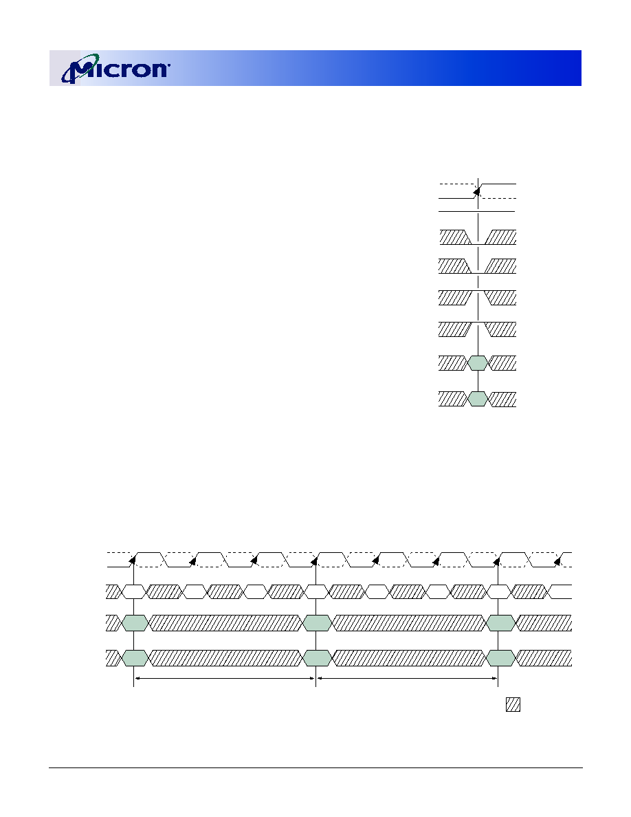
256Mb: x4, x8, x16
DDR SDRAM
09005aef8076894f
Micron Technology, Inc., reserves the right to change products or specifications without notice.
256MBDDRx4x8x16_2.fm - Rev. F 6/03 EN
19
©2003 Micron Technology, Inc.
Operations
Bank/Row Activation
Before any READ or WRITE commands can be
issued to a bank within the DDR SDRAM, a row in that
bank must be "opened." This is accomplished via the
ACTIVE command, which selects both the bank and
the row to be activated, as shown in Figure 10.
After a row is opened with an ACTIVE command, a
READ or WRITE command may be issued to that row,
subject to the
t
RCD specification.
t
RCD (MIN) should
be divided by the clock period and rounded up to the
next whole number to determine the earliest clock
edge after the ACTIVE command on which a READ or
WRITE command can be entered. For example, a
t
RCD
specification of 20ns with a 133 MHz clock (7.5ns
period) results in 2.7 clocks rounded to 3. This is
reflected in Figure 11, which covers any case where 2 <
t
RCD (MIN)/
t
CK
£ 3. (Figure 11 also shows the same
case for
t
RRD; the same procedure is used to convert
other specification limits from time units to clock
cycles.)
A subsequent ACTIVE command to a different row
in the same bank can only be issued after the previous
active row has been "closed" (precharged). The mini-
mum time interval between successive ACTIVE com-
mands to the same bank is defined by
t
RC.
A subsequent ACTIVE command to another bank
can be issued while the first bank is being accessed,
which results in a reduction of total row-access over-
head. The minimum time interval between successive
ACTIVE commands to different banks is defined by
t
RRD.
Figure 10: Activating a Specific Row in
a Specific Bank
Figure 11: Example: Meeting
t
RCD (
t
RRD) MIN When 2 <
t
RCD (
t
RRD) MIN/
t
CK
£ 3
CS#
WE#
CAS#
RAS#
CKE
A0≠A12
RA
RA = Row Address
BA = Bank Address
HIGH
BA0, BA1
BA
CK
CK#
t
COMMAND
BA0, BA1
ACT
ACT
NOP
RRD
tRCD
CK
CK#
Bank x
Bank y
A0≠A12
Row
Row
NOP
RD/WR
NOP
Bank y
Col
NOP
T0
T1
T2
T3
T4
T5
T6
T7
DON'T CARE
NOP

256Mb: x4, x8, x16
DDR SDRAM
09005aef8076894f
Micron Technology, Inc., reserves the right to change products or specifications without notice.
256MBDDRx4x8x16_2.fm - Rev. F 6/03 EN
20
©2003 Micron Technology, Inc.
READs
READ bursts are initiated with a READ command, as
shown in Figure 12 on page 21.
The starting column and bank addresses are pro-
vided with the READ command and auto precharge is
either enabled or disabled for that burst access. If auto
precharge is enabled, the row being accessed is pre-
charged at the completion of the burst.
NOTE:
For the READ commands used in the follow-
ing illustrations, auto precharge is disabled.
During READ bursts, the valid data-out element
from the starting column address will be available fol-
lowing the CAS latency after the READ command.
Each subsequent data-out element will be valid nomi-
nally at the next positive or negative clock edge (i.e., at
the next crossing of CK and CK#). Figure 13 on page 22
shows general timing for each possible CAS latency
setting. DQS is driven by the DDR SDRAM along with
output data. The initial LOW state on DQS is known as
the read preamble; the LOW state coincident with the
last data-out element is known as the read postamble.
Upon completion of a burst, assuming no other
commands have been initiated, the DQs will go High-
Z. A detailed explanation of
t
DQSQ (valid data-out
skew),
t
QH (data-out window hold), and the valid data
window are depicted in Figure 40 on page 65 and
Figure 41 on page 66. A detailed explanation of
t
DQSCK (DQS transition skew to CK) and
t
AC (data-out
transition skew to CK) is depicted in Figure 42 on
page 67.
Data from any READ burst may be concatenated
with or truncated with data from a subsequent READ
command. In either case, a continuous flow of data
can be maintained. The first data element from the
new burst follows either the last element of a com-
pleted burst or the last desired data element of a longer
burst which is being truncated. The new READ com-
mand should be issued x cycles after the first READ
command, where x equals the number of desired data
element pairs (pairs are required by the 2n-prefetch
architecture). This is shown in Figure 14 on page 23. A
READ command can be initiated on any clock cycle
following a previous READ command. Nonconsecutive
read data is illustrated in Figure 15, Nonconsecutive
READ Bursts, on page 24. Full-speed random read
accesses within a page (or pages) can be performed as
shown in Figure 16, Random READ Accesses, on
page 25.
Data from any READ burst may be truncated with a
BURST TERMINATE command, as shown in Figure 17
on page 26. The BURST TERMINATE latency is equal
to the read (CAS) latency; i.e., the BURST TERMINATE
command should be issued x cycles after the READ
command, where x equals the number of desired data
element pairs (pairs are required by the 2n-prefetch
architecture).
Data from any READ burst must be completed or
truncated before a subsequent WRITE command can
be issued. If truncation is necessary, the BURST TER-
MINATE command must be used, as shown in
Figure 18 on page 27. The
t
DQSS (NOM) case is shown;
the
t
DQSS (MAX) case has a longer bus idle time.
(
t
DQSS [MIN] and
t
DQSS [MAX] are defined in the sec-
tion on WRITEs.)
A READ burst may be followed by, or truncated with,
a PRECHARGE command to the same bank provided
that auto precharge was not activated.
The PRECHARGE command should be issued x
cycles after the READ command, where x equals the
number of desired data element pairs (pairs are
required by the 2n-prefetch architecture). This is
shown in Figure 19 on page 28. Following the PRE-
CHARGE command, a subsequent command to the
same bank cannot be issued until both
t
RAS and
t
RP
have been met. Note that part of the row precharge
time is hidden during the access of the last data ele-
ments.
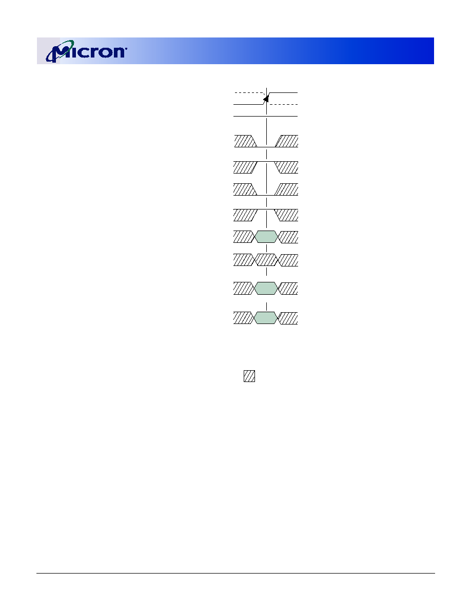
256Mb: x4, x8, x16
DDR SDRAM
09005aef8076894f
Micron Technology, Inc., reserves the right to change products or specifications without notice.
256MBDDRx4x8x16_2.fm - Rev. F 6/03 EN
21
©2003 Micron Technology, Inc.
Figure 12: READ Command
CS#
WE#
CAS#
RAS#
CKE
CA
x4: A0≠A9, A11
x8: A0≠A9
x16: A0≠A8
A10
BA0,1
HIGH
EN AP
DIS AP
BA
x4: A12
x8: A11, A12
x16: A9, A11, A12
CK
CK#
CA = Column Address
BA = Bank Address
EN AP = Enable Auto Precharge
DIS AP = Disable Auto Precharge
DON'T CARE
256Mb: x4, x8, x16
DDR SDRAM
09005aef8076894f
Micron Technology, Inc., reserves the right to change products or specifications without notice.
256MBDDRx4x8x16_2.fm - Rev. F 6/03 EN
22
©2003 Micron Technology, Inc.
Figure 13: READ Burst
NOTE:
1. DO n = data-out from column n.
2. Burst length = 4.
3. Three subsequent elements of data-out appear in the programmed order following DO n.
4. Shown with nominal
t
AC,
t
DQSCK, and
t
DQSQ.
CK
CK#
COMMAND
READ
NOP
NOP
NOP
NOP
NOP
ADDRESS
Bank a,
Col n
READ
NOP
NOP
NOP
NOP
NOP
Bank a,
Col n
CL = 2
CK
CK#
COMMAND
ADDRESS
DQ
DQS
CL = 2.5
DQ
DQS
DO
n
DO
n
T0
T1
T2
T3
T2n
T3n
T4
T5
T0
T1
T2
T3
T2n
T3n
T4
T5
DON'T CARE
TRANSITIONING DATA

256Mb: x4, x8, x16
DDR SDRAM
09005aef8076894f
Micron Technology, Inc., reserves the right to change products or specifications without notice.
256MBDDRx4x8x16_2.fm - Rev. F 6/03 EN
23
©2003 Micron Technology, Inc.
Figure 14: Consecutive READ Bursts
NOTE:
1. DO n (or b) = data-out from column n (or column b).
2. Burst length = 4 or 8 (if 4, the bursts are concatenated; if 8, the second burst interrupts the first).
3. Three subsequent elements of data-out appear in the programmed order following DO n.
4. Three (or seven) subsequent elements of data-out appear in the programmed order following DO b.
5. Shown with nominal
t
AC,
t
DQSCK, and
t
DQSQ.
6. Example applies only when READ commands are issued to the same device.
CK
CK#
COMMAND
READ
NOP
READ
NOP
NOP
NOP
ADDRESS
Bank,
Col n
Bank,
Col b
COMMAND
READ
NOP
READ
NOP
NOP
NOP
ADDRESS
Bank,
Col n
Bank,
Col b
CL = 2
CK
CK#
COMMAND
ADDRESS
DQ
DQS
CL = 2.5
DQ
DQS
DO
n
DO
b
DO
n
DO
b
T0
T1
T2
T3
T2n
T3n
T4
T5
T4n
T5n
T0
T1
T2
T3
T2n
T3n
T4
T5
T4n
T5n
DON'T CARE
TRANSITIONING DATA

256Mb: x4, x8, x16
DDR SDRAM
09005aef8076894f
Micron Technology, Inc., reserves the right to change products or specifications without notice.
256MBDDRx4x8x16_2.fm - Rev. F 6/03 EN
24
©2003 Micron Technology, Inc.
Figure 15: Nonconsecutive READ Bursts
NOTE:
1. DO n (or b) = data-out from column n (or column b).
2. Burst length = 4 or 8 (if 4, the bursts are concatenated; if 8, the second burst interrupts the first).
3. Three subsequent elements of data-out appear in the programmed order following DO n.
4. Three (or seven) subsequent elements of data-out appear in the programmed order following DO b.
5. Shown with nominal
t
AC,
t
DQSCK, and
t
DQSQ.
CK
CK#
COMMAND
READ
NOP
NOP
NOP
NOP
NOP
ADDRESS
Bank,
Col n
READ
Bank,
Col b
COMMAND
ADDRESS
CL = 2
CK
CK#
COMMAND
ADDRESS
DQ
DQS
CL = 2.5
DQ
DQS
DO
n
T0
T1
T2
T3
T2n
T3n
T4
T5
T5n
T6
READ
NOP
NOP
NOP
NOP
NOP
Bank,
Col n
READ
Bank,
Col b
T0
T1
T2
T3
T2n
T3n
T4
T5
T5n
T6
DO
b
DO
n
DO
b
DON'T CARE
TRANSITIONING DATA
256Mb: x4, x8, x16
DDR SDRAM
09005aef8076894f
Micron Technology, Inc., reserves the right to change products or specifications without notice.
256MBDDRx4x8x16_2.fm - Rev. F 6/03 EN
25
©2003 Micron Technology, Inc.
Figure 16: Random READ Accesses
NOTE:
1. DO n (or x or b or g) = data-out from column n (or column x or column b or column g).
2. Burst length = 2, 4 or 8 (if 4 or 8, the following burst interrupts the previous).
3. n' or x' or b' or g' indicates the next data-out following DO n or DO x or DO b or DO g, respectively.
4. READs are to an active row in any bank.
5. Shown with nominal
t
AC,
t
DQSCK, and
t
DQSQ.
CK
CK#
COMMAND
READ
READ
READ
NOP
NOP
ADDRESS
Bank,
Col n
Bank,
Col x
Bank,
Col b
Bank,
Col x
Bank,
Col b
READ
Bank,
Col g
COMMAND
ADDRESS
CL = 2
CK
CK#
COMMAND
ADDRESS
DQ
DQS
CL = 2.5
DQ
DQS
DO
n
DO
x'
DO
g
DO
n'
DO
b
DO
x
DO
b'
DO
n
DO
x'
DO
n'
DO
b
DO
x
DO
b'
T0
T1
T2
T3
T2n
T3n
T4
T5
T4n
T5n
READ
READ
READ
NOP
NOP
Bank,
Col n
READ
Bank,
Col g
T0
T1
T2
T3
T2n
T3n
T4
T5
T4n
T5n
DON'T CARE
TRANSITIONING DATA

256Mb: x4, x8, x16
DDR SDRAM
09005aef8076894f
Micron Technology, Inc., reserves the right to change products or specifications without notice.
256MBDDRx4x8x16_2.fm - Rev. F 6/03 EN
26
©2003 Micron Technology, Inc.
Figure 17: Terminating a READ Burst
NOTE:
1. DO n = data-out from column n.
2. Burst length = 4 or 8.
3. Subsequent element of data-out appears in the programmed order following DO n.
4. Shown with nominal
t
AC,
t
DQSCK, and
t
DQSQ.
5. BST = BURST TERMINATE command; page remains open.
CK
CK#
COMMAND
READ
BST
5
NOP
NOP
NOP
NOP
ADDRESS
Bank a,
Col n
READ
BST
5
NOP
NOP
NOP
NOP
Bank a,
Col n
CL = 2
CK
CK#
COMMAND
ADDRESS
DQ
DQS
CL = 2.5
DQ
DQS
DO
n
DO
n
T0
T1
T2
T3
T2n
T4
T5
T0
T1
T2
T3
T2n
T4
T5
DON'T CARE
TRANSITIONING DATA

256Mb: x4, x8, x16
DDR SDRAM
09005aef8076894f
Micron Technology, Inc., reserves the right to change products or specifications without notice.
256MBDDRx4x8x16_2.fm - Rev. F 6/03 EN
27
©2003 Micron Technology, Inc.
Figure 18: READ to WRITE
NOTE:
1. DO n = data-out from column n.
2. DI b = data-in from column b.
3. Burst length = 4 in the cases shown (applies for bursts of 8 as well; if the burst length is 2, the BST command shown can
be NOP).
4. One subsequent element of data-out appears in the programmed order following DO n.
5. Data-in elements are applied following DI b in the programmed order.
6. Shown with nominal
t
AC,
t
DQSCK, and
t
DQSQ.
7. BST = BURST TERMINATE command;
8. page remains open.
CK
CK#
COMMAND
READ
BST
7
NOP
NOP
NOP
ADDRESS
Bank,
Col n
WRITE
Bank,
Col b
T0
T1
T2
T3
T2n
T4
T5
T4n
T5n
CL = 2
DQ
DQS
DM
t
(NOM)
DQSS
DI
b
CK
CK#
COMMAND
READ
BST
7
NOP
WRITE
NOP
ADDRESS
Bank a,
Col n
NOP
T0
T1
T2
T3
T2n
T4
T5
T5n
CL = 2.5
DQ
DQS
DO
n
DM
DI
b
DON'T CARE
TRANSITIONING DATA
DO
n
t
(NOM)
DQSS
256Mb: x4, x8, x16
DDR SDRAM
09005aef8076894f
Micron Technology, Inc., reserves the right to change products or specifications without notice.
256MBDDRx4x8x16_2.fm - Rev. F 6/03 EN
28
©2003 Micron Technology, Inc.
Figure 19: READ to PRECHARGE
NOTE:
1. DO n = data-out from column n.
2. Burst length = 4, or an interrupted burst of 8.
3. Three subsequent elements of data-out appear in the programmed order following DO n.
4. Shown with nominal
t
AC,
t
DQSCK, and
t
DQSQ.
5. READ to PRECHARGE equals two clocks, which allows two data pairs of data-out.
6. A READ command with AUTO-PRECHARGE enabled, provided
t
RAS (MIN) is met, would cause a precharge to be per-
formed at x number of clock cycles after the READ command, where x = BL / 2.
7. An active command to the same bank is only allowed if
t
RC (MIN) has been satisfied.
8. PRE = PRECHARGE command; ACT = ACTIVE command.
CK
CK#
COMMAND
6
READ
NOP
PRE
NOP
NOP
ACT
ADDRESS
Bank a,
Col n
Bank a,
(a or all)
Bank a,
Row
READ
NOP
PRE
NOP
NOP
ACT
Bank a,
Col n
CL = 2
tRP
tRP
CK
CK#
COMMAND
6
ADDRESS
DQ
DQS
CL = 2.5
DQ
DQS
DO
n
DO
n
T0
T1
T2
T3
T2n
T3n
T4
T5
T0
T1
T2
T3
T2n
T3n
T4
T5
Bank a,
(a or all)
Bank a,
Row
DON'T CARE
TRANSITIONING DATA

256Mb: x4, x8, x16
DDR SDRAM
09005aef8076894f
Micron Technology, Inc., reserves the right to change products or specifications without notice.
256MBDDRx4x8x16_2.fm - Rev. F 6/03 EN
29
©2003 Micron Technology, Inc.
WRITEs
WRITE bursts are initiated with a WRITE command,
as shown in Figure 20.
The starting column and bank addresses are pro-
vided with the WRITE command, and auto precharge
is either enabled or disabled for that access. If auto
precharge is enabled, the row being accessed is pre-
charged at the completion of the burst and after the
t
WR time.
NOTE:
For the WRITE commands used in the follow-
ing illustrations, auto precharge is disabled.
During WRITE bursts, the first valid data-in element
will be registered on the first rising edge of DQS follow-
ing the WRITE command, and subsequent data ele-
ments will be registered on successive edges of DQS.
The LOW state on DQS between the WRITE command
and the first rising edge is known as the write pream-
ble; the LOW state on DQS following the last data-in
element is known as the write postamble.
The time between the WRITE command and the
first corresponding rising edge of DQS (
t
DQSS) is
specified with a relatively wide range (from 75 per-
cent to 125 percent of one clock cycle). All of the
WRITE diagrams show the nominal case, and where
the two extreme cases (i.e.,
t
DQSS [MIN] an
d
t
DQSS
[MAX]) might not be
intuitive, they have also been
included. Figure 21 on page 30 shows the nominal
case and the extremes of
t
DQSS for a burst of 4.
Upon completion of a burst, assuming no other
commands have been initiated, the DQ will remain
High-Z and any additional input data will be
ignored.
Data for any WRITE burst may be concatenated
with or truncated with a subsequent WRITE com-
mand. In either case, a continuous flow of input data
can be maintained. The new WRITE command can be
issued on any positive edge of clock following the pre-
vious WRITE command. The first data element from
the new burst is applied after either the last element of
a completed burst or the last desired data element of a
longer burst which is being truncated. The new WRITE
command should be issued x cycles after the first
WRITE command, where x equals the number of
desired data element pairs (pairs are required by the
2n-prefetch architecture).
Figure 22 on page 31 shows concatenated bursts of
4. An example of nonconsecutive WRITEs is shown in
Figure 23 on page 32. Full-speed random write
accesses within a page or pages can be performed as
shown in Figure 24 on page 33.
Figure 20: WRITE Command
Data for any WRITE burst may be followed by a sub-
sequent READ command. To follow a WRITE without
truncating the WRITE burst,
t
WTR should be met as
shown in Figure 25 on page 34.
Data for any WRITE burst may be truncated by a
subsequent READ command, as shown in Figure 26 on
page 35.
Note that only the data-in pairs that are registered
prior to the
t
WTR period are written to the internal
array, and any subsequent data-in should be masked
with DM, as shown in Figure 27 on page 36.
Data for any WRITE burst may be followed by a sub-
sequent PRECHARGE command. To follow a WRITE
without truncating the WRITE burst,
t
WR should be
met as shown in Figure 28 on page 37.
Data for any WRITE burst may be truncated by a
subsequent PRECHARGE command, as shown in
Figure 29 on page 38 and Figure 30 on page 39. Note
that only the data-in pairs that are registered prior to
the
t
WR period are written to the internal array, and
any subsequent data-in should be masked with DM as
shown in Figures 29 and 30. After the PRECHARGE
command, a subsequent command to the same bank
cannot be issued until
t
RP is met.
CS#
WE#
CAS#
RAS#
CKE
CA
A10
BA0, 1
HIGH
EN AP
DIS AP
BA
CK
CK#
CA = Column Address
BA = Bank Address
EN AP = Enable Auto Precharge
DIS AP = Disable Auto Precharge
DON'T CARE
x4: A0≠A9, A11
x8: A0≠A9
x16: A0≠A8
x4: A12
x8: A11, A12
x16: A9, A11, A12

256Mb: x4, x8, x16
DDR SDRAM
09005aef8076894f
Micron Technology, Inc., reserves the right to change products or specifications without notice.
256MBDDRx4x8x16_2.fm - Rev. F 6/03 EN
30
©2003 Micron Technology, Inc.
Figure 21: WRITE Burst
NOTE:
1. DI b = data-in for column b.
2. Three subsequent elements of data-in are applied in the programmed order following DI b.
3. An uninterrupted burst of 4 is shown.
4. A10 is LOW with the WRITE command (auto precharge is disabled).
DQS
t
DQSS (MAX)
t
DQSS (NOM)
t
DQSS (MIN)
tDQSS
DM
DQ
CK
CK#
COMMAND
WRITE
NOP
NOP
ADDRESS
Bank a,
Col b
NOP
T0
T1
T2
T3
T2n
DQS
tDQSS
DM
DQ
DQS
tDQSS
DM
DQ
DI
b
DI
b
DI
b
DON'T CARE
TRANSITIONING DATA

256Mb: x4, x8, x16
DDR SDRAM
09005aef8076894f
Micron Technology, Inc., reserves the right to change products or specifications without notice.
256MBDDRx4x8x16_2.fm - Rev. F 6/03 EN
31
©2003 Micron Technology, Inc.
Figure 22: Consecutive WRITE to WRITE
NOTE:
1. DI b, etc., = data-in for column b, etc.
2. Three subsequent elements of data-in are applied in the programmed order following DI b.
3. Three subsequent elements of data-in are applied in the programmed order following DI n.
4. An uninterrupted burst of 4 is shown.
5. Each WRITE command may be to any bank.
CK
CK#
COMMAND
WRITE
NOP
WRITE
NOP
NOP
ADDRESS
Bank,
Col b
NOP
Bank,
Col n
T0
T1
T2
T3
T2n
T4
T5
T4n
T3n
T1n
DQ
DQS
DM
DI
n
DI
b
DON'T CARE
TRANSITIONING DATA
t
DQSS
t
DQSS (NOM)
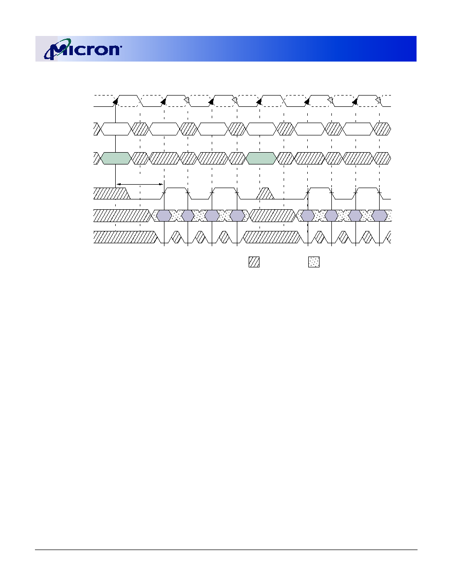
256Mb: x4, x8, x16
DDR SDRAM
09005aef8076894f
Micron Technology, Inc., reserves the right to change products or specifications without notice.
256MBDDRx4x8x16_2.fm - Rev. F 6/03 EN
32
©2003 Micron Technology, Inc.
Figure 23: Nonconsecutive WRITE to WRITE
NOTE:
1. DI b, etc., = data-in for column b, etc.
2. Three subsequent elements of data-in are applied in the programmed order following DI b.
3. Three subsequent elements of data-in are applied in the programmed order following DI n.
4. An uninterrupted burst of 4 is shown.
5. Each WRITE command may be to any bank.
CK
CK#
COMMAND
WRITE
NOP
NOP
NOP
NOP
ADDRESS
Bank,
Col b
WRITE
Bank,
Col n
T0
T1
T2
T3
T2n
T4
T5
T4n
T1n
T5n
DQ
DQS
DM
DI
n
DI
b
t
DQSS (NOM)
t
DQSS
DON'T CARE
TRANSITIONING DATA

256Mb: x4, x8, x16
DDR SDRAM
09005aef8076894f
Micron Technology, Inc., reserves the right to change products or specifications without notice.
256MBDDRx4x8x16_2.fm - Rev. F 6/03 EN
33
©2003 Micron Technology, Inc.
Figure 24: Random WRITE Cycles
NOTE:
1. DI b, etc., = data-in for column b, etc.
2. b', etc., = the next data-in following DI b, etc., according to the programmed burst order.
3. Programmed burst length = 2, 4, or 8 in cases shown.
4. Each WRITE command may be to any bank.
t
DQSS (NOM)
CK
CK#
COMMAND
WRITE
WRITE
WRITE
WRITE
NOP
ADDRESS
Bank,
Col b
Bank,
Col x
Bank,
Col n
Bank,
Col g
WRITE
Bank,
Col a
T0
T1
T2
T3
T2n
T4
T5
T4n
T1n
T3n
T5n
DQ
DQS
DM
DI
b
DI
b'
DI
x
DI
x'
DI
n
DI
n'
DI
a
DI
a'
DI
g
DI
g'
DON'T CARE
TRANSITIONING DATA

256Mb: x4, x8, x16
DDR SDRAM
09005aef8076894f
Micron Technology, Inc., reserves the right to change products or specifications without notice.
256MBDDRx4x8x16_2.fm - Rev. F 6/03 EN
34
©2003 Micron Technology, Inc.
Figure 25: WRITE to READ - Uninterrupting
NOTE:
1. DI b = data-in for column b; DO n = data-out for column n.
2. Three subsequent elements of data-in are applied in the programmed order following DI b.
3. An uninterrupted burst of 4 is shown.
4.
t
WTR is referenced from the first positive CK edge after the last data-in pair.
5. The READ and WRITE commands are to the same device. However, the READ and WRITE commands may be directed to
different devices, in which case,
t
WTR is not required and the READ command could be applied earlier.
6. A10 is LOW with the WRITE command (auto precharge is disabled).
t
DQSS (NOM)
CK
CK#
COMMAND
WRITE
NOP
NOP
READ
NOP
NOP
ADDRESS
Bank a,
Col b
Bank a,
Col n
NOP
T0
T1
T2
T3
T2n
T4
T5
T1n
T6
T6n
t
WTR
CL = 2
DQ
DQS
DM
DI
b
DO
n
t
DQSS
t
DQSS (MIN)
CL = 2
DQ
DQS
DM
DI
b
DO
n
t
DQSS
t
DQSS (MAX)
CL = 2
DQ
DQS
DM
DI
b
DO
n
t
DQSS
DON'T CARE
TRANSITIONING DATA
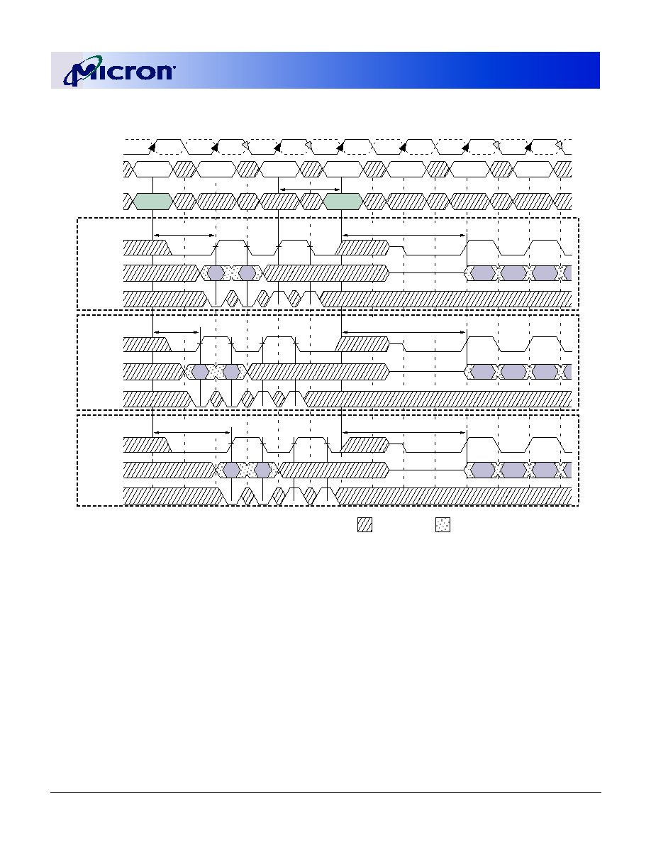
256Mb: x4, x8, x16
DDR SDRAM
09005aef8076894f
Micron Technology, Inc., reserves the right to change products or specifications without notice.
256MBDDRx4x8x16_2.fm - Rev. F 6/03 EN
35
©2003 Micron Technology, Inc.
Figure 26: WRITE to READ ≠ Interrupting
NOTE:
1. DI b = data-in for column ;, DO n = data-out for column n.
2. An interrupted burst of 4 is shown; two data elements are written.
3. One subsequent element of data-in is applied in the programmed order following DI b.
4.
t
WTR is referenced from the first positive CK edge after the last data-in pair.
5. A10 is LOW with the WRITE command (auto precharge is disabled).
6. DQS is required at T2 and T2n (nominal case) to register DM.
7. If the burst of 8 was used, DM and DQS would be required at T3 and T3n because the READ command would not mask
these two data elements.
t
DQSS (NOM)
CK
CK#
COMMAND
WRITE
NOP
NOP
NOP
NOP
NOP
ADDRESS
Bank a,
Col b
Bank a,
Col n
READ
T0
T1
T2
T3
T2n
T4
T5
T5n
T1n
T6
T6n
t
WTR
CL = 2
DQ
DQS
DM
DI
b
DO
n
t
DQSS (MIN)
CL = 2
DQ
DQS
DM
DI
b
t
DQSS (MAX)
CL = 2
DQ
DQS
DM
DI
b
DO
n
DO
n
DON'T CARE
TRANSITIONING DATA
t
DQSS
t
DQSS
t
DQSS
T3n
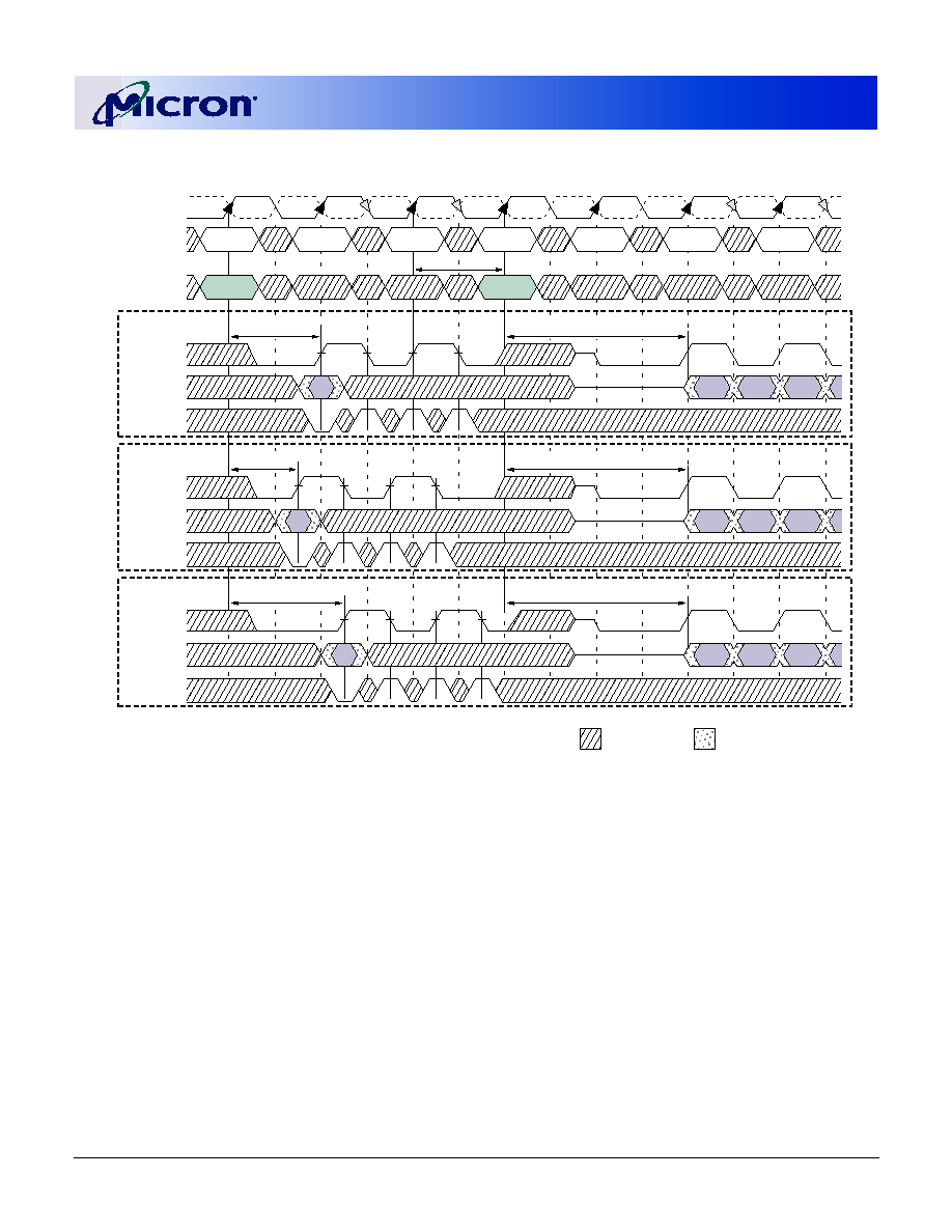
256Mb: x4, x8, x16
DDR SDRAM
09005aef8076894f
Micron Technology, Inc., reserves the right to change products or specifications without notice.
256MBDDRx4x8x16_2.fm - Rev. F 6/03 EN
36
©2003 Micron Technology, Inc.
Figure 27: WRITE to READ ≠ Odd Number of Data, Interrupting
NOTE:
1. DI b = data-in for column b; DO n = data-out for column n.
2. An interrupted burst of 4 is shown; one data element is written.
3.
t
WTR is referenced from the first positive CK edge after the last desired data-in pair (not the last two data elements).
4. A10 is LOW with the WRITE command (auto precharge is disabled).
5. DQS is required at T1n, T2, and T2n (nominal case) to register DM.
6. If the burst of 8 was used, DM and DQS would be required at T3≠T3n because the READ command would not mask these
data elements.
t
DQSS (NOM)
CK
CK#
COMMAND
WRITE
NOP
NOP
NOP
NOP
NOP
ADDRESS
Bank a,
Col b
Bank a,
Col n
READ
T0
T1
T2
T3
T2n
T4
T5
T1n
T6
T6n
T5n
t
WTR
CL = 2
DQ
DQS
DM
DI
b
DO
n
t
DQSS (MIN)
CL = 2
DQ
DQS
DM
DI
b
DO
n
t
DQSS (MAX)
CL = 2
DQ
DQS
DM
DI
b
DO
n
DON'T CARE
TRANSITIONING DATA
t
DQSS
t
DQSS
t
DQSS
T3n
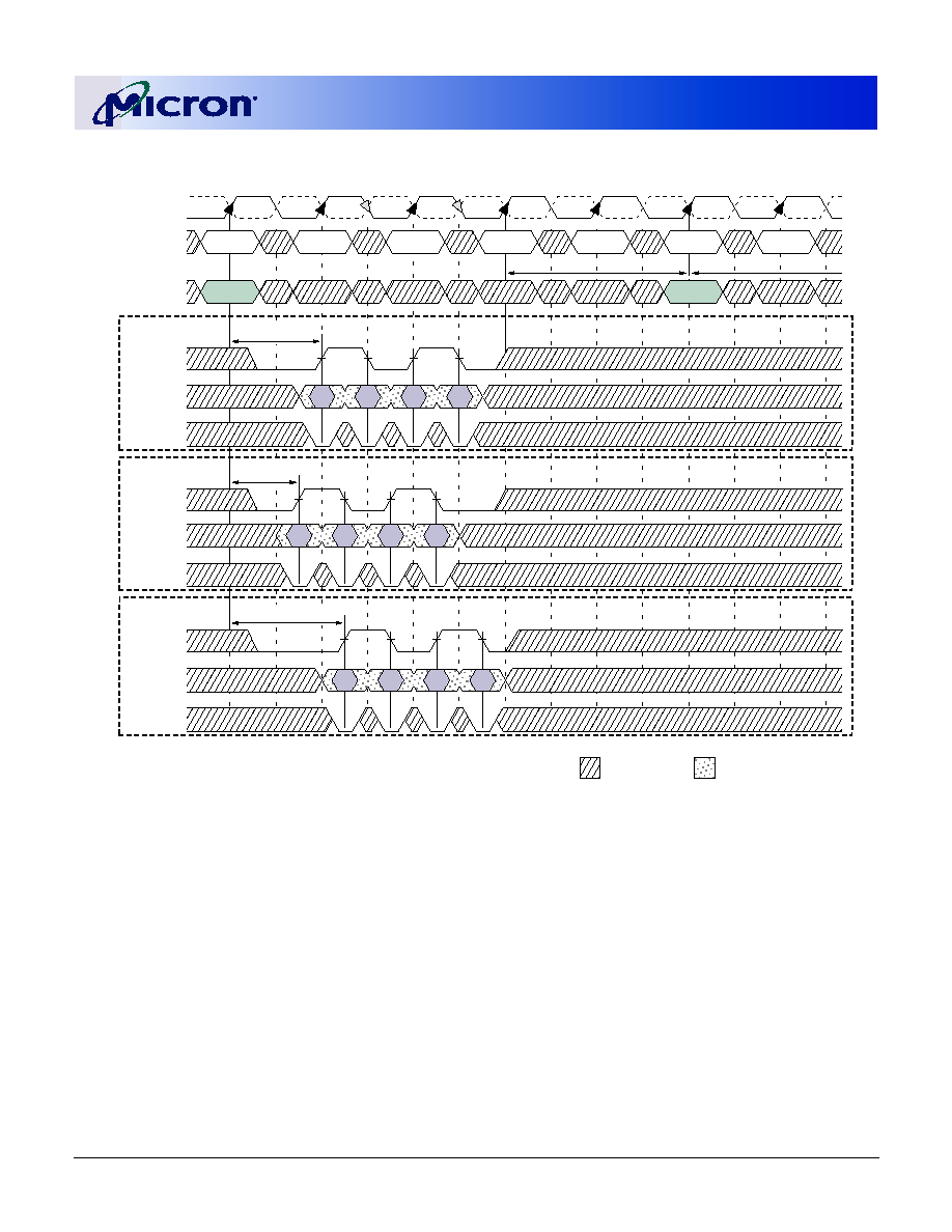
256Mb: x4, x8, x16
DDR SDRAM
09005aef8076894f
Micron Technology, Inc., reserves the right to change products or specifications without notice.
256MBDDRx4x8x16_2.fm - Rev. F 6/03 EN
37
©2003 Micron Technology, Inc.
Figure 28: WRITE to PRECHARGE - Uninterrupting
NOTE:
1. DI b = data-in for column b.
2. Three subsequent elements of data-in are applied in the programmed order following DI b.
3. An uninterrupted burst of 4 is shown.
4.
t
WR is referenced from the first positive CK edge after the last data-in pair.
5. The PRECHARGE and WRITE commands are to the same device. However, the PRECHARGE and WRITE commands may be
to different devices, in which case,
t
WR is not required and the PRECHARGE command could be applied earlier.
6. A10 is LOW with the WRITE command (auto precharge is disabled).
7. PRE = PRECHARGE command.
t
DQSS (NOM)
CK
CK#
COMMAND
WRITE
NOP
NOP
NOP
PRE
7
NOP
ADDRESS
Bank a,
Col b
Bank,
(a or all)
NOP
T0
T1
T2
T3
T2n
T4
T5
T1n
T6
t
WR
t
RP
DQ
DQS
DM
DI
b
t
DQSS (MIN)
DQ
DQS
DM
DI
b
t
DQSS (MAX)
DQ
DQS
DM
DI
b
DON'T CARE
TRANSITIONING DATA
t
DQSS
t
DQSS
t
DQSS
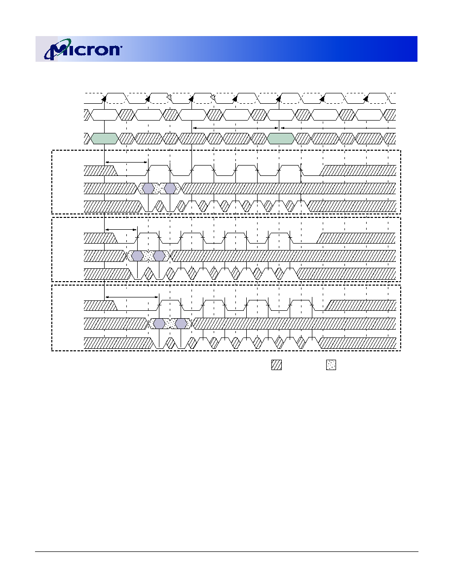
256Mb: x4, x8, x16
DDR SDRAM
09005aef8076894f
Micron Technology, Inc., reserves the right to change products or specifications without notice.
256MBDDRx4x8x16_2.fm - Rev. F 6/03 EN
38
©2003 Micron Technology, Inc.
Figure 29: WRITE to PRECHARGE ≠ Interrupting
NOTE:
1. DI b = data-in for column b.
2. Subsequent element of data-in is applied in the programmed order following DI b.
3. An interrupted burst of 8 is shown; two data elements are written.
4.
t
WR is referenced from the first positive CK edge after the last data-in pair.
5. A10 is LOW with the WRITE command (auto precharge is disabled).
6. DQS is required at T4 and T4n (nominal case) to register DM.
7. If the burst of 4 was used, DQS and DM would not be required at T3, T3n, T4, and T4n.
8. PRE = PRECHARGE command.
t
DQSS
t
DQSS (NOM)
CK
CK#
COMMAND
WRITE
NOP
NOP
PRE
8
NOP
NOP
ADDRESS
Bank a,
Col b
Bank,
(a or all)
NOP
T0
T1
T2
T3
T2n
T4
T5
T1n
T6
t
WR
t
RP
DQ
DQS
DM
DI
b
t
DQSS
t
DQSS (MIN)
DQ
DQS
DM
DI
b
t
DQSS
t
DQSS (MAX)
DQ
DQS
DM
DI
b
DON'T CARE
TRANSITIONING DATA
T3n
T4n

256Mb: x4, x8, x16
DDR SDRAM
09005aef8076894f
Micron Technology, Inc., reserves the right to change products or specifications without notice.
256MBDDRx4x8x16_2.fm - Rev. F 6/03 EN
39
©2003 Micron Technology, Inc.
Figure 30: WRITE to PRECHARGE ≠ Odd Number of Data ≠ Interrupting
NOTE:
1. DI b = data-in for column b.
2. An interrupted burst of 8 is shown; one data element is written.
3.
t
WR is referenced from the first positive CK edge after the last data-in pair.
4. A10 is LOW with the WRITE command (auto precharge is disabled).
5. DQS is required at T4 and T4n (nominal case) to register DM.
6. If the burst of 4 was used, DQS and DM would not be required at T3, T3n, T4, and T4n.
7. PRE = PRECHARGE command.
t
DQSS
t
DQSS (NOM)
CK
CK#
COMMAND
WRITE
NOP
NOP
PRE
7
NOP
NOP
ADDRESS
Bank a,
Col b
Bank,
(a or all)
NOP
T0
T1
T2
T3
T2n
T4
T5
T1n
T6
t
WR
t
RP
DQ
DQS
DM
DI
b
t
DQSS
t
DQSS (MIN)
DQ
DQS
DM
t
DQSS
t
DQSS (MAX)
DQ
DQS
DM
DI
b
DI
b
DON'T CARE
TRANSITIONING DATA
T3n
T4n
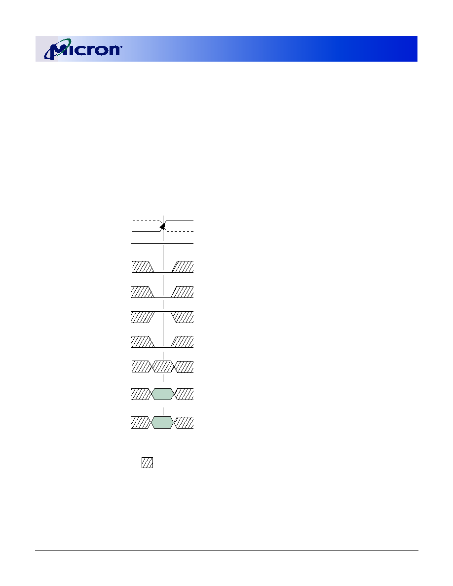
256Mb: x4, x8, x16
DDR SDRAM
09005aef8076894f
Micron Technology, Inc., reserves the right to change products or specifications without notice.
256MBDDRx4x8x16_2.fm - Rev. F 6/03 EN
40
©2003 Micron Technology, Inc.
PRECHARGE
The PRECHARGE command, as shown in Figure 31,
is used to deactivate the open row in a particular bank
or the open row in all banks. The bank(s) will be avail-
able for a subsequent row access some specified time
(
t
RP) after the PRECHARGE command is issued. Input
A10 determines whether one or all banks are to be pre-
charged, and in the case where only one bank is to be
precharged, inputs BA0, BA1 select the bank. When all
banks are to be precharged, inputs BA0, BA1 are
treated as "Don't Care." Once a bank has been pre-
charged, it is in the idle state and must be activated
prior to any READ or WRITE commands being issued
to that bank.
Figure 31: PRECHARGE Command
Power-Down (CKE Not Active)
Unlike SDR SDRAMs, DDR SDRAMs require CKE to
be active at all times that an access is in progress, from
the issuing of a READ or WRITE command until com-
pletion of the access. Thus, a clock suspend is not sup-
ported. For READs, an access completion is defined
when the read postamble is satisfied; for WRITEs, an
access completion is defined when the write recovery
time (
t
WR) is satisfied.
Power-down, shown in Figure 32, Power-Down, on
page 41, is entered when CKE is registered LOW and all
of the criteria listed in Table 8, on page 41, are met. If
power-down occurs when all banks are idle, this mode
is referred to as precharge power-down; if power-down
occurs when there is a row active in any bank, this
mode is referred to as active power-down. Entering
power-down deactivates the input and output buffers,
excluding CK, CK#, and CKE. For maximum power sav-
ings, the DLL is frozen during precharge power-down
mode. Exiting power-down requires the device to be at
the same voltage and frequency as when it entered
power-down. However, power-down duration is lim-
ited by the refresh requirements of the device (
t
REFC).
While in power-down, CKE LOW and a stable clock
signal must be maintained at the inputs of the DDR
SDRAM, while all other input signals are "Don't Care."
The power-down state is synchronously exited when
CKE is registered HIGH (in conjunction with a NOP or
DESELECT command). A valid executable command
may be applied one clock cycle later.
CS#
WE#
CAS#
RAS#
CKE
A10
BA0,1
HIGH
ALL BANKS
ONE BANK
BA
A0≠A9, A11, A12
CK
CK#
BA = Bank Address (if A10 is LOW;
otherwise "Don't Care")
DON'T CARE
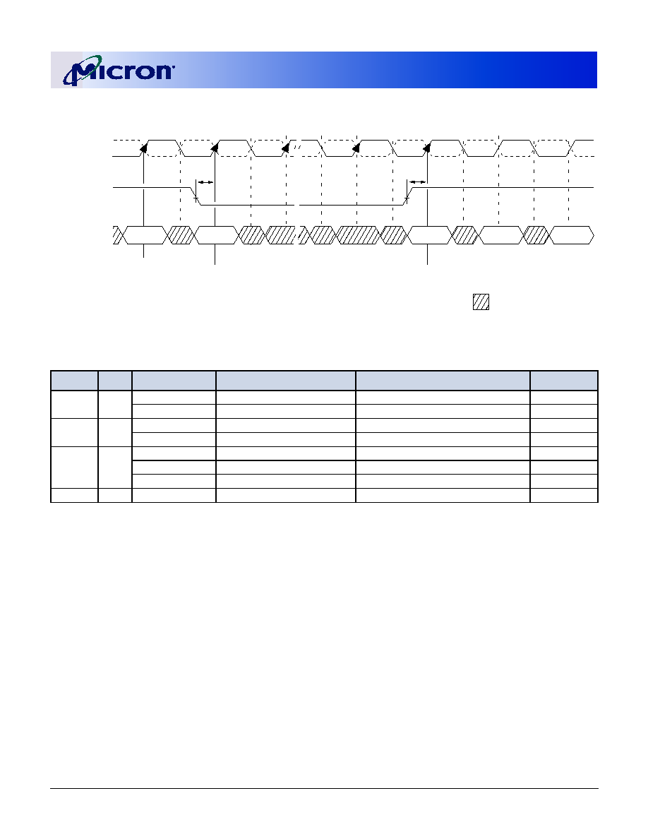
256Mb: x4, x8, x16
DDR SDRAM
09005aef8076894f
Micron Technology, Inc., reserves the right to change products or specifications without notice.
256MBDDRx4x8x16_2.fm - Rev. F 6/03 EN
41
©2003 Micron Technology, Inc.
Figure 32: Power-Down
NOTE:
1. CKE
n
is the logic state of CKE at clock edge n; CKE
n-1
was the state of CKE at the previous clock edge.
2. Current state is the state of the DDR SDRAM immediately prior to clock edge n.
3. COMMAND
n
is the command registered at clock edge n, and ACTION
n
is a result of COMMAND
n
.
4. All states and sequences not shown are illegal or reserved.
5. CKE must not drop LOW during a column access. For a READ, this means CKE must stay HIGH until after the read postam-
ble time; for a WRITE, CKE must stay HIGH until the WRITE recovery time (
t
WR) has been met.
6. Once initialized, including during self refresh mode, V
REF
must be powered within the specified range.
7. Upon exit of the self refresh mode, the DLL is automatically enabled, but a DLL reset must still occur. A minimum of 200
clock cycles is needed before applying a READ command for the DLL to lock. DESELECT or NOP commands should be
issued on any clock edges occurring during the
t
XSNR period.
t
IS
t
IS
No READ/WRITE
access in progress
Exit power-down mode
Enter power-down mode
CKE
CK
CK#
COMMAND
NOP
(
)
(
)
(
)
(
)
(
)
(
)
(
)
(
)
(
)
(
)
NOP
VALID
T0
T1
T2
Ta0
Ta1
Ta2
VALID
DON'T CARE
VALID
Table 8:
Truth Table ≠ CKE
Notes: 1≠6
CKE
n-1
CKE
n
CURRENT STATE
COMMAND
n
ACTION
n
NOTES
L
L
Power-Down
X
Maintain Power-Down
Self Refresh
X
Maintain Self Refresh
L
H
Power-Down
DESELECT or NOP
Exit Power-Down
Self Refresh
DESELECT or NOP
Exit Self Refresh
7
H
L
All Banks Idle
DESELECT or NOP
Precharge Power-Down Entry
Bank(s) Active
DESELECT or NOP
Active Power-Down Entry
All Banks Idle
AUTO REFRESH
Self Refresh Entry
H
H
See Table 9 on page 42

256Mb: x4, x8, x16
DDR SDRAM
09005aef8076894f
Micron Technology, Inc., reserves the right to change products or specifications without notice.
256MBDDRx4x8x16_2.fm - Rev. F 6/03 EN
42
©2003 Micron Technology, Inc.
NOTE:
1. This table applies when CKE
n-1
was HIGH and CKE
n
is HIGH (see Table 8 on page 41) and after
t
XSNR has been met (if the
previous state was self refresh).
2. This table is bank-specific, except where noted (i.e., the current state is for a specific bank and the commands shown are
those allowed to be issued to that bank when in that state). Exceptions are covered in the notes below.
3. Current state definitions:
Idle:
The bank has been precharged, and
t
RP has been met.
Row Active: A row in the bank has been activated, and
t
RCD has been met. No data bursts/accesses and no register
accesses are in progress.
Read:
A READ burst has been initiated, with auto precharge disabled, and has not yet terminated or been termi-
nated.
Write:
A WRITE burst has been initiated, with auto precharge disabled, and has not yet terminated or been ter-
minated.
4. The following states must not be interrupted by a command issued to the same bank. COMMAND INHIBIT or NOP com-
mands, or allowable commands to the other bank should be issued on any clock edge occurring during these states.
Allowable commands to the other bank are determined by its current state and Table 9, Truth Table ≠ Current State Bank
n ≠ Command to Bank n, on page 42 and according to Table 10, Truth Table ≠ Current State Bank n≠ Command to Bank
m, on page 44.
Precharging: Starts with registration of a PRECHARGE command and ends when
t
RP is met. Once
t
RP is met, the bank
will be in the idle state.
Row
Activating:
Starts with registration of an ACTIVE command and ends when
t
RCD is met. Once
t
RCD is met, the bank
will be in the "row active" state.
Read w/Auto-Precharge
Enabled:
Starts with registration of a READ command with auto precharge enabled and ends when
t
RP has been-
met. Once
t
RP is met, the bank will be in the idle state.
Write w/Auto- Precharge
Enabled:
Starts with registration of a WRITE command with auto precharge enabled and ends when
t
RP has been
met. Once
t
RP is met, the bank will be in the idle state.
Table 9:
Truth Table ≠ Current State Bank n ≠ Command to Bank n
Notes: 1≠6; notes appear below and on next page
CURRENT STATE
CS#
RAS#
CAS#
WE#
COMMAND/ACTION
NOTES
Any
H
X
X
X
DESELECT (NOP/continue previous operation)
L
H
H
H
NO OPERATION (NOP/continue previous operation)
Idle
L
L
H
H
ACTIVE (select and activate row)
L
L
L
H
AUTO REFRESH
7
L
L
L
L
LOAD MODE REGISTER
7
Row Active
L
H
L
H
READ (select column and start READ burst)
10
L
H
L
L
WRITE (select column and start WRITE burst)
10
L
L
H
L
PRECHARGE (deactivate row in bank or banks)
8
Read
(Auto-
Precharge
Disabled)
L
H
L
H
READ (select column and start new READ burst)
10
L
H
L
L
WRITE (select column and start WRITE burst)
10, 12
L
L
H
L
PRECHARGE (truncate READ burst, start PRECHARGE)
8
L
H
H
L
BURST TERMINATE
9
Write
(Auto-
Precharge
Disabled)
L
H
L
H
READ (select column and start READ burst)
10, 11
L
H
L
L
WRITE (select column and start new WRITE burst)
10
L
L
H
L
PRECHARGE (truncate WRITE burst, start PRECHARGE)
8, 11

256Mb: x4, x8, x16
DDR SDRAM
09005aef8076894f
Micron Technology, Inc., reserves the right to change products or specifications without notice.
256MBDDRx4x8x16_2.fm - Rev. F 6/03 EN
43
©2003 Micron Technology, Inc.
5. The following states must not be interrupted by any executable command; COMMAND INHIBIT or NOP commands must
be applied on each positive clock edge during these states.
Refreshing:
Starts with registration of an AUTO REFRESH command and ends when
t
RFC is met. Once
t
RFC is met, the
DDR SDRAM will be in the all banks idle state.
Accessing Mode
Register:
Starts with registration of a LOAD MODE REGISTER command and ends when
t
MRD has been met. Once
t
MRD is met, the DDR SDRAM will be in the all banks idle state.
Precharging
All:
Starts with registration of a PRECHARGE ALL command and ends when
t
RP is met. Once
t
RP is met, all
banks will be in the idle state.
6. All states and sequences not shown are illegal or reserved.
7. Not bank-specific; requires that all banks are idle and bursts are not in progress.
8. May or may not be bank-specific; if multiple banks are to be precharged, each must be in a valid state for precharging.
9. Not bank-specific; BURST TERMINATE affects the most recent READ burst, regardless of bank.
10.READs or WRITEs listed in the Command/Action column include READs or WRITEs with auto precharge enabled and
READs or WRITEs with auto precharge disabled.
11.Requires appropriate DM masking.
12.A WRITE command may be applied after the completion of the READ burst; otherwise, a BURST TERMINATE must be
used to end the READ burst prior to asserting a WRITE command.
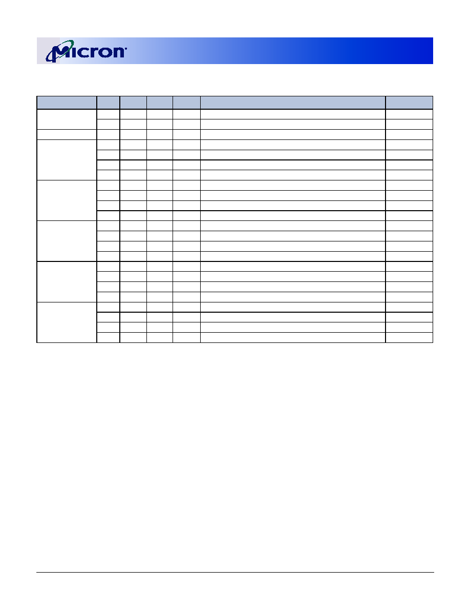
256Mb: x4, x8, x16
DDR SDRAM
09005aef8076894f
Micron Technology, Inc., reserves the right to change products or specifications without notice.
256MBDDRx4x8x16_2.fm - Rev. F 6/03 EN
44
©2003 Micron Technology, Inc.
NOTE:
1. This table applies when CKE
n-1
was HIGH and CKE
n
is HIGH (see Truth Table 2) and after
t
XSNR has been met (if the previ-
ous state was self refresh).
2. This table describes alternate bank operation except where noted (i.e., the current state is for bank n and the commands
shown are those allowed to be issued to bank m, assuming that bank m is in such a state that the given command is
allowable). Exceptions are covered in the notes below.
3. Current state definitions:
Idle:
The bank has been precharged, and
t
RP has been met.
Row Active: A row in the bank has been activated, and
t
RCD has been met. No data bursts/accesses and no register
accesses are in progress.
Read:
A READ burst has been initiated, with auto precharge disabled, and has not yet terminated or been termi-
nated.
Write:
A WRITE burst has been initiated, with auto precharge disabled, and has not yet terminated or been ter-
minated
Read with Auto Precharge Enabled: See following text ≠ 3a
Write with Auto Precharge Enabled: See following text ≠ 3a
a. The read with auto precharge enabled or write with auto precharge enabled states can each be broken into two
parts: the access period and the precharge period. For read with auto precharge, the precharge period is defined as if
the same burst was executed with auto precharge disabled and then followed with the earliest possible PRECHARGE
command that still accesses all of the data in the burst. For write with auto precharge, the precharge period begins
when
t
WR ends, with
t
WR measured as if auto precharge was disabled. The access period starts with registration of
the command and ends where the precharge period (or
t
RP) begins.
Table 10: Truth Table ≠ Current State Bank n≠ Command to Bank m
Notes: 1≠6; notes appear below and on next page
CURRENT STATE
CS#
RAS#
CAS#
WE#
COMMAND/ACTION
NOTES
Any
H
X
X
X
DESELECT (NOP/continue previous operation)
L
H
H
H
NO OPERATION (NOP/continue previous operation)
Idle
X
X
X
X
Any Command Otherwise Allowed to Bank m
Row
Activating,
Active, or
Precharging
L
L
H
H
ACTIVE (select and activate row)
L
H
L
H
READ (select column and start READ burst)
7
L
H
L
L
WRITE (select column and start WRITE burst)
7
L
L
H
L
PRECHARGE
Read
(Auto-Precharge
Disabled)
L
L
H
H
ACTIVE (select and activate row)
L
H
L
H
READ (select column and start new READ burst)
7
L
H
L
L
WRITE (select column and start WRITE burst)
7, 9
L
L
H
L
PRECHARGE
Write
(Auto- Precharge
Disabled)
L
L
H
H
ACTIVE (select and activate row)
L
H
L
H
READ (select column and start READ burst)
7, 8
L
H
L
L
WRITE (select column and start new WRITE burst)
7
L
L
H
L
PRECHARGE
Read
(With Auto-
Precharge)
L
L
H
H
ACTIVE (select and activate row)
L
H
L
H
READ (select column and start new READ burst)
7, 3a
L
H
L
L
WRITE (select column and start WRITE burst)
7, 9, 3a
L
L
H
L
PRECHARGE
Write
(With Auto-
Precharge)
L
L
H
H
ACTIVE (select and activate row)
L
H
L
H
READ (select column and start READ burst)
7, 3a
L
H
L
L
WRITE (select column and start new WRITE burst)
7, 3a
L
L
H
L
PRECHARGE
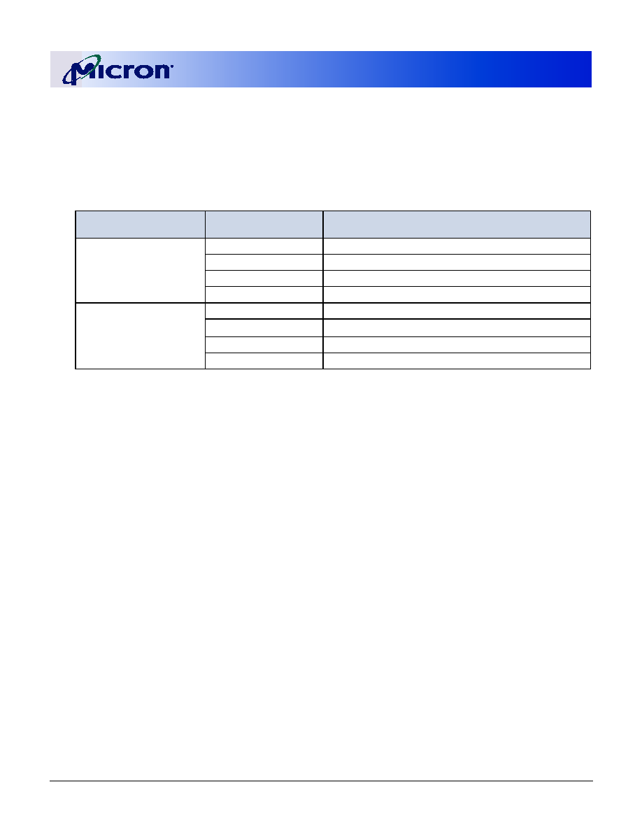
256Mb: x4, x8, x16
DDR SDRAM
09005aef8076894f
Micron Technology, Inc., reserves the right to change products or specifications without notice.
256MBDDRx4x8x16_2.fm - Rev. F 6/03 EN
45
©2003 Micron Technology, Inc.
This device supports concurrent auto precharge such that when a READ with auto precharge is enabled or a WRITE
with auto precharge is enabled any command to other banks is allowed, as long as that command does not interrupt
the read or write data transfer already in process. In either case, all other related limitations apply (e.g., contention
between read data and write data must be avoided).
b. The minimum delay from a READ or WRITE command with auto precharge enabled, to a command to a different
bank, is summarized below.
NOTE:
CL
RU
= CAS Latency (CL) rounded up to the next integer
BL = Bust length
4. AUTO REFRESH and LOAD MODE REGISTER commands may only be issued when all banks are idle.
5. A BURST TERMINATE command cannot be issued to another bank; it applies to the bank represented by the current state
only.
6. All states and sequences not shown are illegal or reserved.
7. READs or WRITEs listed in the Command/Action column include READs or WRITEs with auto precharge enabled and
READs or WRITEs with auto precharge disabled.
8. Requires appropriate DM masking.
9. A WRITE command may be applied after the completion of the READ burst; otherwise, a BURST TERMINATE must be
used to end the READ burst prior to asserting a WRITE command.
FROM COMMAND
TO COMMAND
MINIMUM DELAY
(WITH CONCURRENT AUTO PRECHARGE)
WRITE w/AP
READ or READ w/AP
[1 + (BL/2)] *
t
CK +
t
WTR
WRITE or WRITE w/AP
(BL/2) *
t
CK
PRECHARGE
1
t
CK
ACTIVE
1
t
CK
READ w/AP
READ or READ w/AP
(BL/2) *
t
CK
WRITE or WRITE w/AP
[CL
RU
+
(BL/2)] *
t
CK
PRECHARGE
1
t
CK
ACTIVE
1
t
CK

256Mb: x4, x8, x16
DDR SDRAM
09005aef8076894f
Micron Technology, Inc., reserves the right to change products or specifications without notice.
256MBDDRx4x8x16_2.fm - Rev. F 6/03 EN
46
©2003 Micron Technology, Inc.
Absolute Maximum Ratings
Stresses greater than those listed may cause perma-
nent damage to the device. This is a stress rating only,
and functional operation of the device at these or any
other conditions above those indicated in the opera-
tional sections of this specification is not implied.
Exposure to absolute maximum rating conditions for
extended periods may affect reliability.
V
DD
Supply Voltage
Relative to Vss ...................................... -1V to +3.6V
V
DD
Q Supply Voltage
Relative to V
SS
..................................... -1V to +3.6V
V
REF
and Inputs Voltage
Relative to V
SS
..................................... -1V to +3.6V
I/O Pins Voltage
Relative to V
SS
....................... -0.5V to V
DD
Q +0.5V
Operating Temperature, T
A
(ambient, Commercial) ..................... 0įC to +70įC
Operating Temperature, T
A
(ambient, Industrial).......................-40įC to +85įC
Storage Temperature (plastic) ...............-55įC to +150įC
Power Dissipation........................................................ 1W
Short Circuit Output Current .................................50mA
Table 11: DC Electrical Characteristics and Operating Conditions
0įC
£ T
A
£ +70įC; V
DD
Q = +2.5V Ī0.2V, V
DD
= +2.5V Ī0.2V
Notes: 1≠5, 16; notes appear on pages 59≠62
PARAMETER/CONDITION
SYMBOL
MIN
MAX
UNITS
NOTES
Supply Voltage
V
DD
2.3
2.7
V
36, 41,
46
I/O Supply Voltage
V
DD
Q
2.3
2.7
V
36, 41,
44,46
I/O Reference Voltage
V
REF
0.49 x V
DD
Q
0.51 x V
DD
Q
V
6, 44
I/O Termination Voltage (system)
V
TT
V
REF
- 0.04
V
REF
+ 0.04
V
7, 44
Input High (Logic 1) Voltage
V
IH
(
DC
)
V
REF
+ 0.15
V
DD
+ 0.3
V
28
Input Low (Logic 0) Voltage
V
IL
(
DC
)
-0.3
V
REF
- 0.15
V
28
INPUT LEAKAGE CURRENT
Any input 0V
£ V
IN
£ V
DD
, V
REF
PIN 0V
£ VIN £ 1.35V
(All other pins not under test = 0V)
I
I
-2
2
ĶA
OUTPUT LEAKAGE CURRENT
(DQs are disabled; 0V
£ VOUT £
V
DD
Q
)
I
OZ
-5
5
ĶA
OUTPUT LEVELS: Full drive option - x4, x8, x16
High Current (V
OUT
= V
DD
Q - 0.373V, minimum V
REF
,
minimum V
TT
)
I
OH
-16.8
-
mA
37, 39
Low Current (V
OUT
= 0.373V, maximum V
REF
, maximum V
TT
)
I
OL
16.8
-
mA
OUTPUT LEVELS: Reduced drive option - x16 only
High Current (V
OUT
= V
DD
Q - 0.763V, minimum V
REF
,
minimum V
TT
)
I
OHR
-9
-
mA
38, 39
Low Current (V
OUT
= 0.763V, maximum V
REF
, maximum V
TT
)
I
OLR
9
-
mA
Table 12: AC Input Operating Conditions
0įC
£ T
A
£ +70įC; V
DD
Q = +2.5V Ī0.2V, V
DD
= +2.5V Ī0.2V
Notes: 1≠5, 14, 16; notes appear on pages 59≠62
PARAMETER/CONDITION
SYMBOL
MIN
MAX
UNITS
NOTES
Input High (Logic 1) Voltage
V
IH
(
AC
)
V
REF
+ 0.310
-
V
14, 28, 40
Input Low (Logic 0) Voltage
V
IL
(
AC
)
-
V
REF
- 0.310
V
14, 28, 40
I/O Reference Voltage
V
REF
(
AC
)
0.49 x V
DD
Q
0.51 x V
DD
Q
V
6
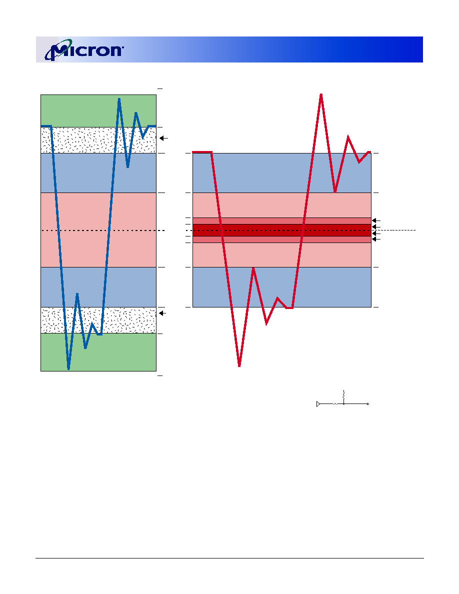
256Mb: x4, x8, x16
DDR SDRAM
09005aef8076894f
Micron Technology, Inc., reserves the right to change products or specifications without notice.
256MBDDRx4x8x16_2.fm - Rev. F 6/03 EN
47
©2003 Micron Technology, Inc.
Figure 33: Input Voltage Waveform
0.940V
1.100V
1.200V
1.225V
1.250V
1.275V
1.300V
1.400V
1.560V
V
IL
AC
V
IL
DC
V
REF
-AC Noise
V
REF
-DC Error
V
REF
+DC Error
V
REF
+AC Noise
Receiver
Transmitter
V
IH
DC
V
IH
AC
V
OH (MIN)
(1.670V
1
for SSTL_2 termination)
V
IN
AC - Provides margin
between
V
OL
(MAX)
and
V
ILAC
V
SS
Q
V
DD
Q (2.3V minimum)
V
OL
(MAX) (0.83V
2
for
SSTL_2 termination)
System Noise Margin (Power/Ground,
Crosstalk, Signal Integrity Attenuation)
NOTE:
1. V
OH
(MIN) with test load is 1.927V
2. V
OL
(MAX) with test load is 0.373V
3. Numbers in diagram reflect nomimal
values utilizing circuit below.
Reference
Point
25
25
V
TT
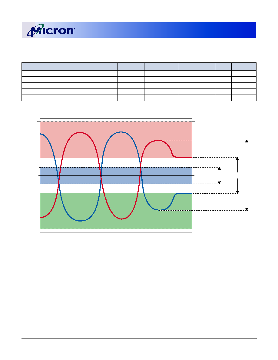
256Mb: x4, x8, x16
DDR SDRAM
09005aef8076894f
Micron Technology, Inc., reserves the right to change products or specifications without notice.
256MBDDRx4x8x16_2.fm - Rev. F 6/03 EN
48
©2003 Micron Technology, Inc.
Figure 34: SSTL_2 Clock Input
NOTE:
1.
This provides a minimum of 1.15V to a maximum of 1.35V and is always half of V
DD
Q.
2. CK and CK# must cross in this region.
3.
CK and CK# must meet at least V
ID
(DC) MIN when static and is centered around V
MP
(DC)
4. CK and CK# must have a minimum 700mv peak-to-peak swing.
5.
CK or CK# may not be more positive than V
DD
Q + 0.3V or more negative than Vss - 0.3V.
6. For AC operation, all DC clock requirements must also be satisfied.
7. Numbers in diagram reflect nominal values.
Table 13: Clock Input Operating Conditions
0įC
£ T
A
£ +70įC; V
DD
Q = +2.5V Ī0.2V, V
DD
= +2.5V Ī0.2V
Notes: 1≠5, 15, 16, 30; notes appear on pages 59≠62
PARAMETER/CONDITION
SYMBOL
MIN
MAX
UNITS
NOTES
Clock Input Midpoint Voltage; CK and CK#
V
MP
(
DC
)
1.15
1.35
V
6, 9
Clock Input Voltage Level; CK and CK#
V
IN
(
DC
)
-0.3
V
DD
Q + 0.3
V
6
Clock Input Differential Voltage; CK and CK#
V
ID
(
DC
)
0.36
V
DD
Q + 0.6
V
6, 8
Clock Input Differential Voltage; CK and CK#
V
ID
(
AC
)
0.7
V
DD
Q + 0.6
V
8
Clock Input Crossing Point Voltage; CK and CK#
V
IX
(
AC
)
0.5 x V
DD
Q - 0.2 0.5 x V
DD
Q + 0.2
V
9
CK
CK#
2.80V
2
3
5
5
Maximum Clock Level
Minimum Clock Level
4
- 0.30V
1.25V
1.45V
1.05V
V
ID
(AC)
V
ID
(DC)
X
1
V
MP
(DC)
V
IX
(AC)
X

256Mb: x4, x8, x16
DDR SDRAM
09005aef8076894f
Micron Technology, Inc., reserves the right to change products or specifications without notice.
256MBDDRx4x8x16_2.fm - Rev. F 6/03 EN
49
©2003 Micron Technology, Inc.
Table 14: Capacitance (x4, x8 TSOP)
Note: 13; notes appear on pages 59≠62
PARAMETER
SYMBOL
MIN
MAX
UNITS
NOTES
Delta Input/Output Capacitance: DQ0≠DQ3 (x4), DQ0≠DQ7 (x8)
DC
IO
≠
0.50
pF
24
Delta Input Capacitance: Command and Address
DC
I
1
≠
0.50
pF
29
Delta Input Capacitance: CK, CK#
DC
I
2
≠
0.25
pF
29
Input/Output Capacitance: DQs, DQS, DM
C
IO
4.0
5.0
pF
Input Capacitance: Command and Address
C
I
1
2.0
3.0
pF
Input Capacitance: CK, CK#
C
I
2
2.0
3.0
pF
Input Capacitance: CKE
C
I
3
2.0
3.0
pF
Table 15: Capacitance (x4, x8 FBGA)
Note: 13; notes appear on pages 59≠62
PARAMETER
SYMBOL
MIN
MAX
UNITS
NOTES
Delta Input/Output Capacitance: DQs, DQS, DM
DC
IO
≠
0.50
pF
24
Delta Input Capacitance: Command and Address
DC
I
1
≠
0.50
pF
29
Delta Input Capacitance: CK, CK#
DC
I
2
≠
0.25
pF
29
Input/Output Capacitance: DQs, DQS, DM
C
IO
3.5
4.5
pF
Input Capacitance: Command and Address
C
I
1
1.5
2.5
pF
Input Capacitance: CK, CK#
C
I
2
1.5
2.5
pF
Input Capacitance: CKE
C
I
3
1.5
2.5
pF
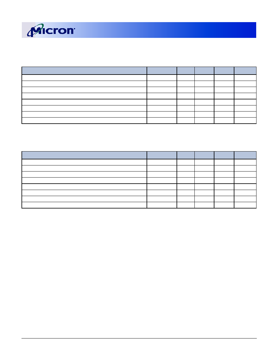
256Mb: x4, x8, x16
DDR SDRAM
09005aef8076894f
Micron Technology, Inc., reserves the right to change products or specifications without notice.
256MBDDRx4x8x16_2.fm - Rev. F 6/03 EN
50
©2003 Micron Technology, Inc.
Table 16: Capacitance (x16 TSOP)
Note: 13; notes appear on pages 59≠62
PARAMETER
SYMBOL
MIN
MAX
UNITS
NOTES
Delta Input/Output Capacitance: DQ0≠DQ7, LDQS, LDM
DC
IOL
≠
0.50
pF
24
Delta Input/Output Capacitance: DQ8≠DQ15, UDQS, UDM
DC
IOU
≠
0.50
pF
24
Delta Input Capacitance: Command and Address
DC
I
1
≠
0.50
pF
29
Delta Input Capacitance: CK, CK#
DC
I
2
≠
0.25
pF
29
Input/Output Capacitance: DQ, LDQS, UDQS, LDM, UDM
C
IO
4.0
5.0
pF
Input Capacitance: Command and Address
C
I
1
2.0
3.0
pF
Input Capacitance: CK, CK#
C
I
2
2.0
3.0
pF
Input Capacitance: CKE
C
I
3
2.0
3.0
pF
Table 17: Capacitance (x16 FBGA)
Note: 13; notes appear onpages 59≠62
PARAMETER
SYMBOL
MIN
MAX
UNITS
NOTES
Delta Input/Output Capacitance: DQ0≠DQ7, LDQS, LDM
DC
IOL
≠
0.50
pF
24
Delta Input/Output Capacitance: DQ8≠DQ15, UDQS, UDM
DC
IOU
≠
0.50
pF
24
Delta Input Capacitance: Command and Address
DC
I
1
≠
0.50
pF
29
Delta Input Capacitance: CK, CK#
DC
I
2
≠
0.25
pF
29
Input/Output Capacitance: DQ, LDQS, UDQS, LDM, UDM
C
IO
3.5
4.5
pF
Input Capacitance: Command and Address
C
I
1
1.5
2.5
pF
Input Capacitance: CK, CK#
C
I
2
1.5
2.5
pF
Input Capacitance: CKE
C
I
3
1.5
2.5
pF
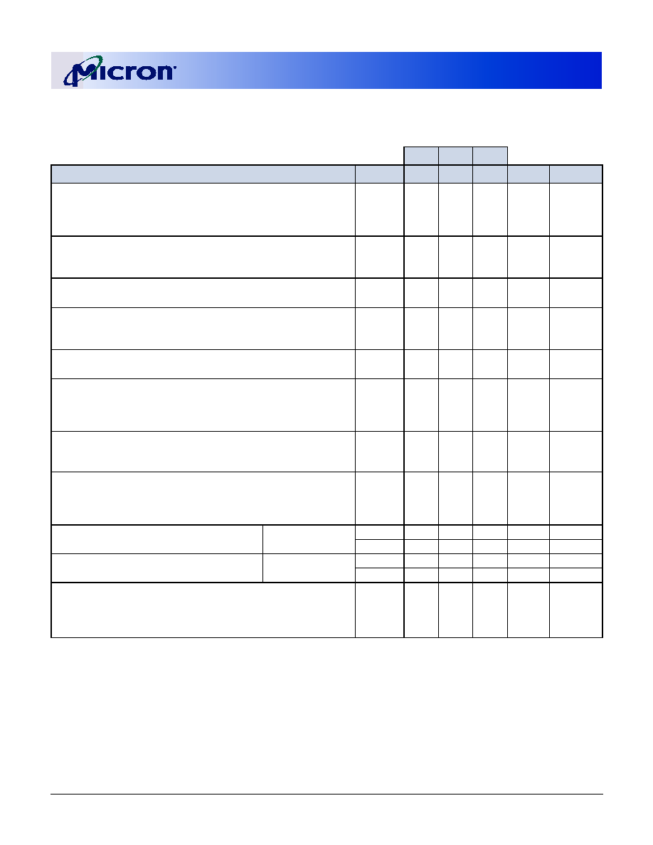
256Mb: x4, x8, x16
DDR SDRAM
09005aef8076894f
Micron Technology, Inc., reserves the right to change products or specifications without notice.
256MBDDRx4x8x16_2.fm - Rev. F 6/03 EN
51
©2003 Micron Technology, Inc.
Table 18: I
DD
Specifications and Conditions (x4, x8; -6/-6R/-6T/-75E)
0įC
£ T
A
£ +70įC; V
DD
Q = +2.5V Ī0.2V, V
DD
= +2.5V Ī0.2V
Notes: 1≠5, 10, 12, 14, 47; notes appear on pages 59≠62; See also Table 22, I
DD
Test Cycle Times, on page 55
MAX
PARAMETER/CONDITION
SYMBOL
-6R
-6/6T
-75E
UNITS
NOTES
OPERATING CURRENT: One bank; active precharge;
t
RC =
t
RC (MIN);
t
CK =
t
CK (MIN); DQ, DM, and DQS inputs
changing once per clock cycle; address and control inputs changing
once every two clock cycles
I
DD
0
155
125
125
mA
22, 48
OPERATING CURRENT: One bank; active-read precharge;
burst = 4;
t
RC =
t
RC (MIN);
t
CK =
t
CK (MIN); I
OUT
= 0mA; address
and control inputs
changing once per clock cycle
I
DD
1
210
170
160
mA
22, 48
PRECHARGE POWER-DOWN STANDBY CURRENT: All banks idle;
power-down mode;
t
CK =
t
CK (MIN); CKE = (LOW)
I
DD
2P
5
4
4
mA
23, 32, 50
IDLE STANDBY CURRENT: CS# = HIGH; all banks are idle;
t
CK =
t
CK (MIN);
CKE = HIGH; address and other control inputs
changing once per clock
cycle; V
IN
= V
REF
for DQ, DQS, and DM
I
DD
2F
50
50
45
mA
51
ACTIVE POWER-DOWN STANDBY CURRENT: One bank active;
power-down mode;
t
CK =
t
CK (MIN); CKE = LOW
I
DD
3P
40
30
25
mA
23, 32, 50
ACTIVE STANDBY CURRENT: CS# = HIGH; CKE = HIGH;
one bank active
;
t
RC =
t
RAS (MAX);
t
CK =
t
CK (MIN); DQ, DM, and
DQS inputs changing twice per clock cycle; address and other
control inputs changing once per clock cycle
I
DD
3N
60
60
50
mA
22
OPERATING CURRENT: Burst = 2;
READs; continuous burst;
one bank active; address and control inputs changing once per
clock cycle;
t
CK =
t
CK (MIN);
I
OUT
= 0mA
I
DD
4R
215
175
150
mA
22, 48
OPERATING CURRENT: Burst = 2; WRITEs; continuous burst;
one bank
active; address and control inputs changing once per
clock cycle;
t
CK =
t
CK (MIN); DQ, DM, and DQS inputs changing
twice per clock cycle
I
DD
4W
235
155
135
mA
22
AUTO REFRESH BURST CURRENT:
t
RC =
t
REFC (MIN)
I
DD
5
264
255
235
mA
50
t
REFC = 7.8Ķs
I
DD
5A
6
6
6
mA
27, 50
SELF REFRESH CURRENT: CKE
£ 0.2V
Standard
I
DD
6
5
4
4
mA
11
Low power (L)
I
DD
6A
N/A
2
2
mA
11
OPERATING CURRENT: Four-bank interleaving READs
(Burst = 4) with auto precharge,
t
RC = minimum
t
RC allowed;
t
CK =
t
CK (MIN); address and control inputs change only during
active READ or WRITE commands
I
DD
7
470
405
350
mA
22, 49
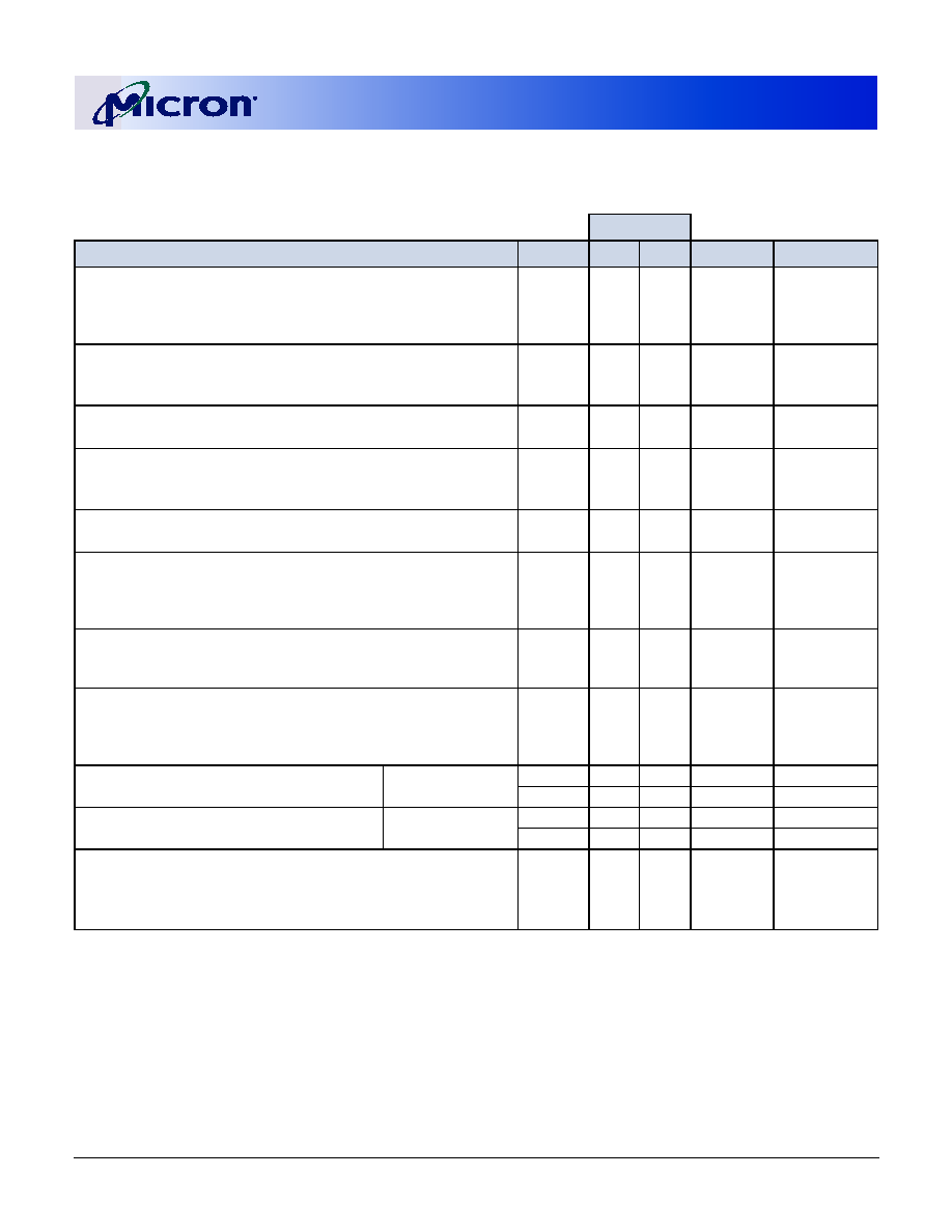
256Mb: x4, x8, x16
DDR SDRAM
09005aef8076894f
Micron Technology, Inc., reserves the right to change products or specifications without notice.
256MBDDRx4x8x16_2.fm - Rev. F 6/03 EN
52
©2003 Micron Technology, Inc.
Table 19: I
DD
Specifications and Conditions (x4, x8; -75Z/-75)
0įC
£ T
A
£ +70įC; V
DD
Q = +2.5V Ī0.2V, V
DD
= +2.5V Ī0.2V
Notes: 1≠5, 10, 12, 14, 47; notes appear on pages 59≠62; See also Table 22, I
DD
Test Cycle Times, on page 55
MAX
PARAMETER/CONDITION
SYMBOL
-75Z
-75
UNITS
NOTES
OPERATING CURRENT: One bank; active precharge;
t
RC =
t
RC (MIN);
t
CK =
t
CK (MIN); DQ, DM, and DQS inputs
changing once per clock cycle; address and control inputs changing
once every two clock cycles
I
DD
0
105
120
mA
22, 48
OPERATING CURRENT: One bank; active-read precharge;
burst = 4;
t
RC =
t
RC (MIN);
t
CK =
t
CK (MIN); I
OUT
= 0mA; address
and control inputs
changing once per clock cycle
I
DD
1
145
155
mA
22, 48
PRECHARGE POWER-DOWN STANDBY CURRENT: All banks idle;
power-down mode;
t
CK =
t
CK (MIN); CKE = (LOW)
I
DD
2P
4
4
mA
23, 32, 50
IDLE STANDBY CURRENT: CS# = HIGH; all banks are idle;
t
CK =
t
CK (MIN);
CKE = HIGH; address and other control inputs
changing once per clock
cycle; V
IN
= V
REF
for DQ, DQS, and DM
I
DD
2F
45
45
mA
51
ACTIVE POWER-DOWN STANDBY CURRENT: One bank active;
power-down mode;
t
CK =
t
CK (MIN); CKE = LOW
I
DD
3P
25
30
mA
23, 32, 50
ACTIVE STANDBY CURRENT: CS# = HIGH; CKE = HIGH;
one bank active
;
t
RC =
t
RAS (MAX);
t
CK =
t
CK (MIN); DQ, DM, and
DQS inputs changing twice per clock cycle; address and other
control inputs changing once per clock cycle
I
DD
3N
50
50
mA
22
OPERATING CURRENT: Burst = 2;
READs; continuous burst;
one bank active; address and control inputs changing once per
clock cycle;
t
CK =
t
CK (MIN);
I
OUT
= 0mA
I
DD
4R
150
175
mA
22, 48
OPERATING CURRENT: Burst = 2; WRITEs; continuous burst;
one bank
active; address and control inputs changing once per
clock cycle;
t
CK =
t
CK (MIN); DQ, DM, and DQS inputs changing
twice per clock cycle
I
DD
4W
135
190
mA
22
AUTO REFRESH BURST CURRENT:
t
RC =
t
REFC(MIN)
I
DD
5
235
245
mA
50
t
REFC = 7.8Ķs
I
DD
5A
6
6
mA
27, 50
SELF REFRESH CURRENT: CKE
£ 0.2V
Standard
I
DD
6
4
4
mA
11
Low power (L)
I
DD
6A
2
2
mA
11
OPERATING CURRENT: Four-bank interleaving READs
(Burst = 4) with auto precharge,
t
RC = minimum
t
RC allowed;
t
CK =
t
CK (MIN); address and control inputs change only during
active READ or WRITE commands
I
DD
7
350
365
mA
22, 49
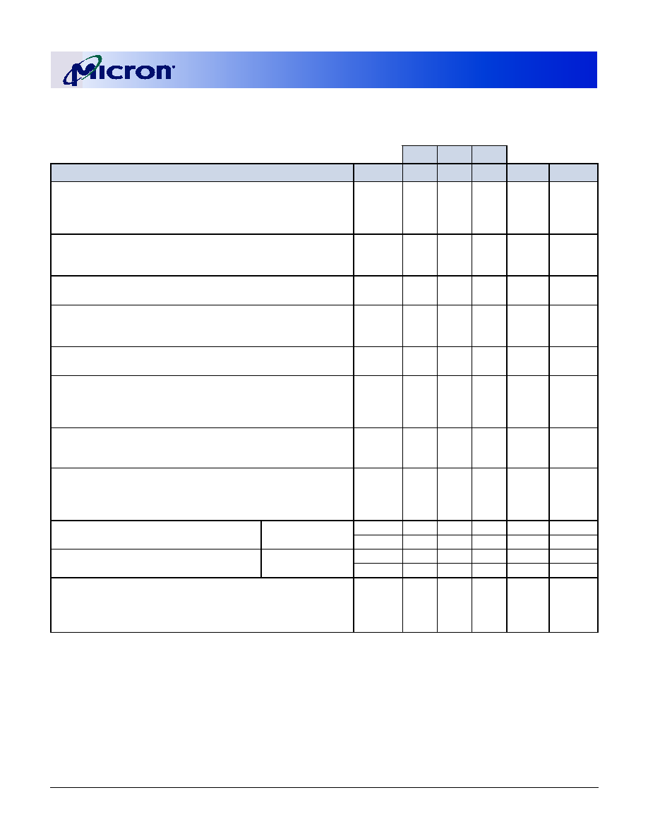
256Mb: x4, x8, x16
DDR SDRAM
09005aef8076894f
Micron Technology, Inc., reserves the right to change products or specifications without notice.
256MBDDRx4x8x16_2.fm - Rev. F 6/03 EN
53
©2003 Micron Technology, Inc.
Table 20: I
DD
Specifications and Conditions (x16; -6/-6R/-6T/-75E)
0įC
£ T
A
£ +70įC; V
DD
Q = +2.5V Ī0.2V, V
DD
= +2.5V Ī0.2V
Notes: 1≠5, 10, 12, 14, 47; notes appear on pages 59≠62; See also Table 22, I
DD
Test Cycle Times, on page 55
MAX
PARAMETER/CONDITION
SYMBOL
-6R
-6/6T
-75E
UNITS
NOTES
OPERATING CURRENT: One bank; active precharge;
t
RC =
t
RC (MIN);
t
CK =
t
CK (MIN); DQ, DM, and DQS inputs
changing once per clock cycle; address and control inputs changing
once every two clock cycles
I
DD
0
155
125
125
mA
22, 48
OPERATING CURRENT: One bank; active-read precharge;
burst = 4;
t
RC =
t
RC (MIN);
t
CK =
t
CK (MIN); I
OUT
= 0mA; address
and control inputs
changing once per clock cycle
I
DD
1
210
180
170
mA
22, 48
PRECHARGE POWER-DOWN STANDBY CURRENT: All banks idle;
power-down mode;
t
CK =
t
CK (MIN); CKE = (LOW)
I
DD
2P
5
4
4
mA
23, 32, 50
IDLE STANDBY CURRENT: CS# = HIGH; all banks are idle;
t
CK =
t
CK (MIN);
CKE = HIGH; address and other control inputs
changing once per clock
cycle; V
IN
= V
REF
for DQ, DQS, and DM
I
DD
2F
50
50
45
mA
51
ACTIVE POWER-DOWN STANDBY CURRENT: One bank active;
power-down mode;
t
CK =
t
CK (MIN); CKE = LOW
I
DD
3P
35
30
25
mA
23, 32, 50
ACTIVE STANDBY CURRENT: CS# = HIGH; CKE = HIGH;
one bank active
;
t
RC =
t
RAS (MAX);
t
CK =
t
CK (MIN); DQ, DM, and
DQS inputs changing twice per clock cycle; address and other
control inputs changing once per clock cycle
I
DD
3N
60
60
50
mA
22
OPERATING CURRENT: Burst = 2;
READs; continuous burst;
one bank active; address and control inputs changing once per
clock cycle;
t
CK =
t
CK (MIN);
I
OUT
= 0mA
I
DD
4R
225
220
185
mA
22, 48
OPERATING CURRENT: Burst = 2; WRITEs; continuous burst;
one bank
active; address and control inputs changing once per
clock cycle;
t
CK =
t
CK (MIN); DQ, DM, and DQS inputs changing
twice per clock cycle
I
DD
4W
250
165
145
mA
22
AUTO REFRESH BURST CURRENT:
t
RC =
t
REFC (MIN)
I
DD
5
265
255
235
mA
50
t
REFC = 7.8Ķs
I
DD
5A
8
6
6
mA
27, 50
SELF REFRESH CURRENT: CKE
£ 0.2V
Standard
I
DD
6
5
4
4
mA
11
Low power (L)
I
DD
6A
NA
2
2
mA
11
OPERATING CURRENT: Four-bank interleaving READs
(Burst = 4) with auto precharge,
t
RC = minimum
t
RC allowed;
t
CK =
t
CK (MIN); address and control inputs change only during
active READ or WRITE commands
I
DD
7
480
440
380
mA
22, 49
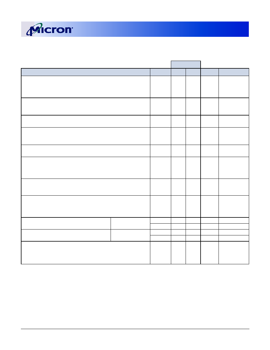
256Mb: x4, x8, x16
DDR SDRAM
09005aef8076894f
Micron Technology, Inc., reserves the right to change products or specifications without notice.
256MBDDRx4x8x16_2.fm - Rev. F 6/03 EN
54
©2003 Micron Technology, Inc.
Table 21: I
DD
Specifications and Conditions (x16; -75Z/-75)
0įC
£ T
A
£ +70įC; V
DD
Q = +2.5V Ī0.2V, V
DD
= +2.5V Ī0.2V
Notes: 1≠5, 10, 12, 14, 47; notes appear on pages 59≠62; See also Table 22, I
DD
Test Cycle Times, on page 55
MAX
PARAMETER/CONDITION
SYMBOL
-75Z
-75
UNITS
NOTES
OPERATING CURRENT: One bank; active precharge;
t
RC =
t
RC (MIN);
t
CK =
t
CK (MIN); DQ, DM, and DQS inputs changing
once per clock cycle; address and control inputs changing once every
two clock cycles
I
DD
0
105
120
mA
22, 48
OPERATING CURRENT: One bank; active-read precharge;
burst = 4;
t
RC =
t
RC (MIN);
t
CK =
t
CK (MIN); I
OUT
= 0mA; address
and control inputs
changing once per clock cycle
I
DD
1
155
165
mA
22, 48
PRECHARGE POWER-DOWN STANDBY CURRENT: All banks idle;
power-down mode;
t
CK =
t
CK (MIN); CKE = (LOW)
I
DD
2P
4
4
mA
23, 32, 50
IDLE STANDBY CURRENT: CS# = HIGH; all banks are idle;
t
CK =
t
CK (MIN);
CKE = HIGH; address and other control inputs
changing once per clock
cycle; V
IN
= V
REF
for DQ, DQS, and DM
I
DD
2F
45
45
mA
51
ACTIVE POWER-DOWN STANDBY CURRENT: One bank active;
power-down mode;
t
CK =
t
CK (MIN); CKE = LOW
I
DD
3P
25
30
mA
23, 32, 50
ACTIVE STANDBY CURRENT: CS# = HIGH; CKE = HIGH;
one bank active
;
t
RC =
t
RAS (MAX);
t
CK =
t
CK (MIN); DQ, DM, and
DQS inputs changing twice per clock cycle; address and other control
inputs changing once per clock cycle
I
DD
3N
50
50
mA
22
OPERATING CURRENT: Burst = 2;
READs; continuous burst;
one bank active; address and control inputs changing once per clock
cycle;
t
CK =
t
CK (MIN);
I
OUT
= 0mA
I
DD
4R
185
250
mA
22, 48
OPERATING CURRENT: Burst = 2; WRITEs; continuous burst;
one bank
active; address and control inputs changing once per clock
cycle;
t
CK =
t
CK (MIN); DQ, DM, and DQS inputs changing twice per
clock cycle
I
DD
4W
145
250
mA
22
AUTO REFRESH BURST CURRENT:
t
RC =
t
REFC (MIN)
I
DD
5
235
245
mA
50
t
REFC = 7.8Ķs
I
DD
5A
6
6
mA
27, 50
SELF REFRESH CURRENT: CKE
£ 0.2V
Standard
I
DD
6
4
4
mA
11
Low power (L)
I
DD
6A
2
2
mA
11
OPERATING CURRENT: Four-bank interleaving READs
(Burst = 4) with auto precharge,
t
RC = minimum
t
RC allowed;
t
CK =
t
CK (MIN); address and control inputs change only during
active READ or WRITE commands
I
DD
7
380
400
mA
22, 49

256Mb: x4, x8, x16
DDR SDRAM
09005aef8076894f
Micron Technology, Inc., reserves the right to change products or specifications without notice.
256MBDDRx4x8x16_2.fm - Rev. F 6/03 EN
55
©2003 Micron Technology, Inc.
Table 22: I
DD
Test Cycle Times
Values reflect number of clock cycles for each test.
IDD TEST
SPEED
GRADE
CLOCK
CYCLE TIME
t
RRD
t
RCD
t
RAS
t
RP
t
RC
t
RFC
t
REFI
CL
I
DD
0
-75/75Z
7.5ns
NA
NA
6
3
9
NA
NA
NA
-75E
7.5ns
NA
NA
6
2
8
NA
NA
NA
-6/6T/6R
6ns
NA
NA
7
3
10
NA
NA
NA
I
DD
1
-75
7.5ns
NA
NA
6
3
9
NA
NA
2.5
-75Z
7.5ns
NA
NA
6
3
9
NA
NA
2
-75E
7.5ns
NA
NA
6
2
8
NA
NA
2
-6/6T/6R
6ns
NA
NA
7
3
10
NA
NA
2.5
I
DD
4R
-75
7.5ns
NA
3
NA
NA
NA
NA
NA
2.5
-75Z
7.5ns
NA
3
NA
NA
NA
NA
NA
2
-75E
7.5ns
NA
2
NA
NA
NA
NA
NA
2
-6/6T/6R
6ns
NA
3
NA
NA
NA
NA
NA
2.5
I
DD
4W
-75
7.5ns
NA
3
NA
NA
NA
NA
NA
NA
-75Z
7.5ns
NA
3
NA
NA
NA
NA
NA
NA
-75E
7.5ns
NA
2
NA
NA
NA
NA
NA
NA
-6/6T/6R
6ns
NA
3
NA
NA
NA
NA
NA
NA
I
DD
5
-75/75Z
7.5ns
NA
NA
NA
3
NA
10
NA
NA
-75E
7.5ns
NA
NA
NA
2
NA
9
NA
NA
-6/6T/6R
6ns
NA
NA
NA
3
NA
12
NA
NA
I
DD
5A
-75/75Z
7.5ns
NA
NA
NA
3
NA
NA
1,030
NA
-75E
7.5ns
NA
NA
NA
2
NA
NA
1,031
NA
-6/6T/6R
6ns
NA
NA
NA
3
NA
NA
1,288
NA
I
DD
7
-75
7.5ns
2/4
3
NA
3
10
NA
NA
2.5
-75Z
7.5ns
2/4
3
NA
3
10
NA
NA
2
-75E
7.5ns
2
3
NA
2
8
NA
NA
2
-6/6T/6R
6ns
2/4
3
NA
3
10
NA
NA
2.5
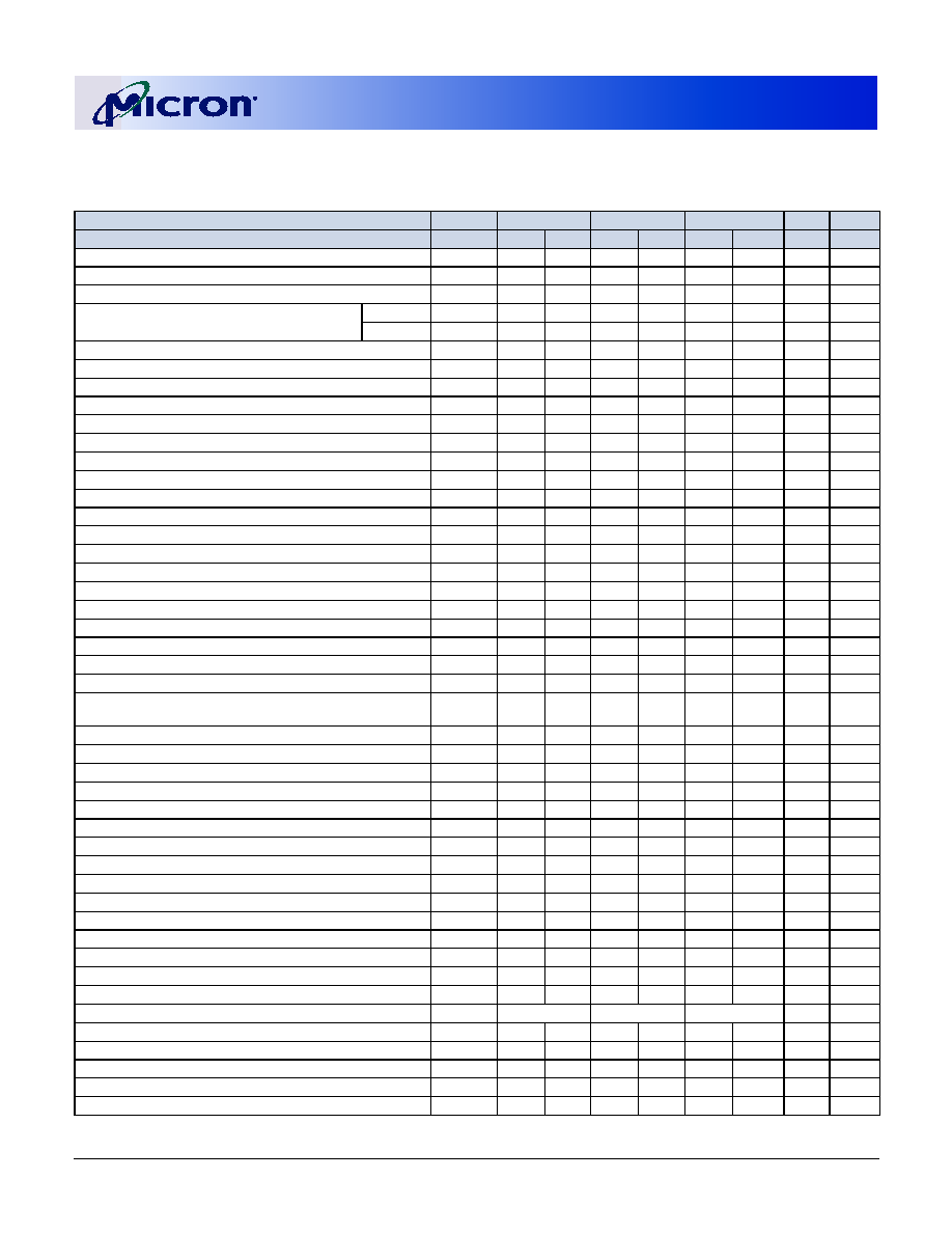
256Mb: x4, x8, x16
DDR SDRAM
09005aef8076894f
Micron Technology, Inc., reserves the right to change products or specifications without notice.
256MBDDRx4x8x16_2.fm - Rev. F 6/03 EN
56
©2003 Micron Technology, Inc.
Table 23: Electrical Characteristics and Recommended AC Operating Conditions
(-6/-6T/-6R/-75E)
Notes: 1≠5, 14≠17, 33, 46; notes appear on pages 59≠62; 0įC
£ T
A
£ +70įC; V
DD
Q = +2.5V Ī0.2V, V
DD
= +2.5V Ī0.2V
AC CHARACTERISTICS
-6 (FBGA)
-6T/6R (TSOP)
-75E
PARAMETER
SYMBOL
MIN
MAX
MIN
MAX
MIN
MAX UNITS NOTES
Access window of DQs from CK/CK#
t
AC
-0.70
+0.70
-0.70
+0.70
-0.75
+0.75
ns
CK high-level width
t
CH
0.45
0.55
0.45
0.55
0.45
0.55
t
CK
30
CK low-level width
t
CL
0.45
0.55
0.45
0.55
0.45
0.55
t
CK
30
Clock cycle time
CL = 2.5
t
CK (2.5)
6
13
6
13
7.5
13
ns
45, 52
CL = 2
t
CK (2)
7.5
13
7.5
13
7.5
13
ns
45, 52
DQ and DM input hold time relative to DQS
t
DH
0.45
0.45
0.5
ns
26, 31
DQ and DM input setup time relative to DQS
t
DS
0.45
0.45
0.5
ns
26, 31
DQ and DM input pulse width (for each input)
t
DIPW
1.75
1.75
1.75
ns
31
Access window of DQS from CK/CK#
t
DQSCK
-0.6
+0.6
-0.6
+0.6
-0.75
+0.75
ns
DQS input high pulse width
t
DQSH
0.35
0.35
0.35
t
CK
DQS input low pulse width
t
DQSL
0.35
0.35
0.35
t
CK
DQS≠DQ skew, DQS to last DQ valid, per group, per access
t
DQSQ
0.4
0.45
0.5
ns
25, 26
WRITE command to first DQS latching transition
t
DQSS
0.75
1.25
0.75
1.25
0.75
1.25
t
CK
DQS falling edge to CK rising ≠ setup time
t
DSS
0.2 0.2 0.2
t
CK
DQS falling edge from CK rising ≠ hold time
t
DSH
0.2 0.2 0.2
t
CK
Half clock period
t
HP
t
CH,
t
CL
t
CH,
t
CL
t
CH,
t
CL
ns
34
Data-out high-impedance window from CK/CK#
t
HZ
+0.7
+0.7
+0.75
ns
18,42
Data-out low-impedance window from CK/CK#
t
LZ
-0.7
-0.7
-0.75
ns
18,43
Address and control input hold time (fast slew rate)
t
IH
F
0.75
0.75
0.90
ns
Address and control input setup time (fast slew rate)
t
IS
F
0.75
0.75
0.90
ns
Address and control input hold time (slow slew rate)
t
IH
S
0.8
0.8
1
ns
14
Address and control input setup time (slow slew rate)
t
IS
S
0.8
0.8
1
ns
14
Address and Control input pulse width (for each input)
t
IPW
2.2
2.2
2.2
ns
LOAD MODE REGISTER command cycle time
t
MRD
12
12
15
ns
DQ≠DQS hold, DQS to first DQ to go non-valid, per access
t
QH
t
HP
-
t
QHS
t
HP
-
t
QHS
t
HP
-
t
QHS
ns
25, 26
Data hold skew factor
t
QHS
0.5
0.55
0.75
ns
ACTIVE to PRECHARGE command
t
RAS
42
70,000
42
70,000
40
120,000
ns
35
ACTIVE to READ with auto precharge command
t
RAP
18
18
15
ns
ACTIVE to ACTIVE/AUTO REFRESH command period
t
RC
60
60
60
ns
AUTO REFRESH command period
t
RFC
72
72
75
ns
50
ACTIVE to READ or WRITE delay
t
RCD
18
18
15
ns
PRECHARGE command period
t
RP
18
18
15
ns
DQS read preamble
t
RPRE
0.9
1.1
0.9
1.1
0.9
1.1
t
CK
42
DQS read postamble
t
RPST
0.4
0.6
0.4
0.6
0.4
0.6
t
CK
18
ACTIVE bank a to ACTIVE bank b command
t
RRD
12
12
15
ns
DQS write preamble
t
WPRE
0.25
0.25
0.25
t
CK
DQS write preamble setup time
t
WPRES
0
0
0
ns
20, 21
DQS write postamble
t
WPST
0.4
0.6
0.4
0.6
0.4
0.6
t
CK
19
Write recovery time
t
WR
15
15
15
ns
Internal WRITE to READ command delay
t
WTR
1
1
1
t
CK
Data valid output window (DVW)
N/A
t
QH -
t
DQSQ
t
QH -
t
DQSQ
t
QH -
t
DQSQ
ns
25
REFRESH to REFRESH command interval
t
REFC
70.3
70.3
70.3
Ķs
23
Average periodic refresh interval
t
REFI
7.8
7.8
7.8
Ķs
23
Terminating voltage delay to V
DD
t
VTD
0
0
0
ns
Exit SELF REFRESH to non-READ command
t
XSNR
75
75
75
ns
Exit SELF REFRESH to READ command
t
XSRD
200
200
200
t
CK
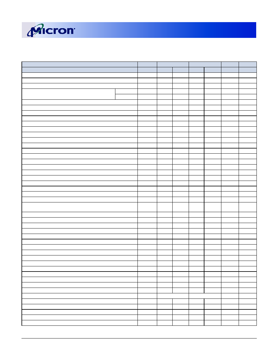
256Mb: x4, x8, x16
DDR SDRAM
09005aef8076894f
Micron Technology, Inc., reserves the right to change products or specifications without notice.
256MBDDRx4x8x16_2.fm - Rev. F 6/03 EN
57
©2003 Micron Technology, Inc.
Table 24: Electrical Characteristics and Recommended AC Operating Conditions
(-75Z/-75)
Notes: 1≠5, 14≠17, 33, 46; notes appear on pages 59≠62; 0įC
£ T
A
£ +70įC; V
DD
Q = +2.5V Ī0.2V, V
DD
= +2.5V Ī0.2V
AC CHARACTERISTICS
-75Z
-75
PARAMETER
SYMBOL
MIN
MAX
MIN
MAX
UNITS
NOTES
Access window of DQs from CK/CK#
t
AC
-0.75
+0.75
-0.75
+0.75
ns
CK high-level width
t
CH
0.45
0.55
0.45
0.55
t
CK
30
CK low-level width
t
CL
0.45
0.55
0.45
0.55
t
CK
30
Clock cycle time
CL=2.5
t
CK (2.5)
7.5
13
7.5
13
ns
45, 52
CL=2
t
CK (2)
7.5
13
10
13
ns
45, 52
DQ and DM input hold time relative to DQS
t
DH
0.50
0.50
ns
26, 31
DQ and DM input setup time relative to DQS
t
DS
0.50
0.50
ns
26, 31
DQ and DM input pulse width (for each input)
t
DIPW
1.75
1.75
ns
31
Access window of DQS from CK/CK#
t
DQSCK
-0.75
+0.75
-0.75
+0.75
ns
DQS input high pulse width
t
DQSH
0.35
0.35
t
CK
DQS input low pulse width
t
DQSL
0.35
0.35
t
CK
DQS≠DQ skew, DQS to last DQ valid, per group, per access
t
DQSQ
0.5
0.5
ns
25, 26
WRITE command to first DQS latching transition
t
DQSS
0.75
1.25
0.75
1.25
t
CK
DQS falling edge to CK rising ≠ setup time
t
DSS
0.20
0.20
t
CK
DQS falling edge from CK rising ≠ hold time
t
DSH
0.20
0.20
t
CK
Half clock period
t
HP
t
CH,
t
CL
t
CH,
t
CL
ns
34
Data-out high-impedance window from CK/CK#
t
HZ
+0.75
+0.75
ns
18,42
Data-out low-impedance window from CK/CK#
t
LZ
-0.75
-0.75
ns
18,43
Address and control input hold time (fast slew rate)
t
IH
F
0.90
0.90
ns
Address and control input setup time (fast slew rate)
t
IS
F
0.90
0.90
ns
Address and control input hold time (slow slew rate)
t
IH
S
1
1
ns
14
Address and control input setup time (slow slew rate)
t
IS
S
1
1
ns
14
Address and Control input pulse width (for each input)
t
IPW
2.2
2.2
ns
LOAD MODE REGISTER command cycle time
t
MRD
15
15
ns
DQ≠DQS hold, DQS to first DQ to go non-valid, per access
t
QH
t
HP
-
t
QHS
t
HP
-
t
QHS
ns
25, 26
Data hold skew factor
t
QHS
0.75
0.75
ns
ACTIVE to PRECHARGE command
t
RAS
40
120,000
40
120,000
ns
35
ACTIVE to READ with auto precharge command
t
RAP
20
20
ns
ACTIVE to ACTIVE/AUTO REFRESH command period
t
RC
65
65
ns
AUTO REFRESH command period
t
RFC
75
75
ns
50
ACTIVE to READ or WRITE delay
t
RCD
20
20
ns
PRECHARGE command period
t
RP
20
20
ns
DQS read preamble
t
RPRE
0.9
1.1
0.9
1.1
t
CK
42
DQS read postamble
t
RPST
0.4
0.6
0.4
0.6
t
CK
18
ACTIVE bank a to ACTIVE bank b command
t
RRD
15
15
ns
DQS write preamble
t
WPRE
0.25
0.25
t
CK
DQS write preamble setup time
t
WPRES
0
0
ns
20, 21
DQS write postamble
t
WPST
0.4
0.6
0.4
0.6
t
CK
19
Write recovery time
t
WR
15
15
ns
Internal WRITE to READ command delay
t
WTR
1
1
t
CK
Data valid output window (DVW)
N/A
t
QH -
t
DQSQ
t
QH -
t
DQSQ
ns
25
REFRESH to REFRESH command interval
t
REFC
70.3
70.3
Ķs
23
Average periodic refresh interval
t
REFI
7.8
7.8
Ķs
23
Terminating voltage delay to V
DD
t
VTD
0
0
ns
Exit SELF REFRESH to non-READ command
t
XSNR
75
75
ns
Exit SELF REFRESH to READ command
t
XSRD
200
200
t
CK
256Mb: x4, x8, x16
DDR SDRAM
09005aef8076894f
Micron Technology, Inc., reserves the right to change products or specifications without notice.
256MBDDRx4x8x16_2.fm - Rev. F 6/03 EN
58
©2003 Micron Technology, Inc.
Table 25: Input Slew Rate Derating Values for Addresses and Commands
0įC
£ T
A
£ +70įC; V
DD
Q = +2.5V Ī0.2V, V
DD
= +2.5V Ī0.2V
Notes: 14; notes appear on pages 59≠62
SPEED
SLEW RATE
t
IS
t
IH
UNITS
-75/-75Z/-75E
0.50 V/ns
£ Slew Rate < 1.0 V/ns
1.00
1
ns
-75/-75Z/-75E
0.40 V/ns
£ Slew Rate < 0.5 V/ns
1.05
1
ns
-75/-75Z/-75E
0.30 V/ns
£ Slew Rate < 0.4 V/ns
1.15
1
ns
Table 26: Input Slew Rate Derating Values for DQ, DQS, and DM
0įC
£ T
A
£ +70įC; V
DD
Q = +2.5V Ī0.2V, V
DD
= +2.5V Ī0.2V
Notes: 31; notes appear on pages 59-62
SPEED
SLEW RATE
T
DS
T
DH
UNITS
-75/-75Z/-75E
0.50 V/ns
£ Slew Rate < 1.0 V/ns
0.50
0.50
ns
-75/-75Z/-75E
0.40 V/ns
£ Slew Rate < 0.5 V/ns
0.55
0.55
ns
-75/-75Z/-75E
0.30 V/ns
£ Slew Rate < 0.4 V/ns
0.60
0.60
ns

256Mb: x4, x8, x16
DDR SDRAM
09005aef8076894f
Micron Technology, Inc., reserves the right to change products or specifications without notice.
256MBDDRx4x8x16_2.fm - Rev. F 6/03 EN
59
©2003 Micron Technology, Inc.
Notes
1. All voltages referenced to V
SS
.
2. Tests for AC timing, I
DD
, and electrical AC and DC
characteristics may be conducted at nominal ref-
erence/supply voltage levels, but the related spec-
ifications and device operation are guaranteed for
the full voltage range specified.
3. Outputs (except for I
DD
measurements) measured
with equivalent load:
4. AC timing and I
DD
tests may use a V
IL
-to-V
IH
swing of up to 1.5V in the test environment, but
input timing is still referenced to V
REF
(or to the
crossing point for CK/CK#), and parameter speci-
fications are guaranteed for the specified AC input
levels under normal use conditions. The mini-
mum slew rate for the input signals used to test
the device is 1 V/ns in the range between V
IL
(AC)
and V
IH
(AC).
5. The AC and DC input level specifications are as
defined in the SSTL_2 standard (i.e., the receiver
will effectively switch as a result of the signal
crossing the AC input level and will remain in that
state as long as the signal does not ring back
above [below] the DC input LOW [HIGH] level).
6. V
REF
is expected to equal V
DD
Q/2 of the transmit-
ting device and to track variations in the DC level
of the same. Peak-to-peak noise (noncommon
mode) on V
REF
may not exceed Ī2 percent of the
DC value. Thus, from V
DD
Q/2, V
REF
is allowed
Ī25mV for DC error and an additional Ī25mV for
AC noise. This measurement is to be taken at the
nearest V
REF
bypass capacitor.
7. V
TT
is not applied directly to the device. V
TT
, a sys-
tem supply for signal termination resistors, is
expected to be set equal to V
REF
and must track
variations in the DC level of V
REF
.
8. V
ID
is the magnitude of the difference between
the input level on CK and the input level on CK#.
9. The value of V
IX
and V
MP
are expected to equal
V
DD
Q/2 of the transmitting device and must track
variations in the DC level of the same.
10. I
DD
is dependent on output loading and cycle
rates. Specified values are obtained with mini-
mum cycle times at CL = 2.5 for -6/-6T/-6R and -
75, and CL = 2 for -75E/-75Z speeds with the out-
puts open.
11. Enables on-chip refresh and address counters.
12. I
DD
specifications are tested after the device is
properly initialized and is averaged at the defined
cycle rate.
13. This parameter is sampled. V
DD
= +2.5VĪ0.2V,
V
DD
Q = +2.5VĪ0.2V, V
REF
= V
SS
, f = 100 MHz, T
A
=
25įC, V
OUT
(DC) = V
DD
Q/2, V
OUT
(peak to peak) =
0.2V. DM input is grouped with I/O pins, reflecting
that they are matched in loading.
14. For slew rates < 1 V/ns and
≥ 0.5 V/ns. If slew rate
is less than 0.5 V/ns, timing must be derated;
t
IS
has an additional 50ps per each 100mV/ns reduc-
tion in slew rate from the 500mV/ns, while
t
IH is
unaffected. If the slew rate exceeds 4.5 V/ns, func-
tionality is uncertain. For -6, -6T, and -6R, slew
rates must be greater than or equal to 0.5V/ns.
15. The CK/CK# input reference level (for timing ref-
erenced to CK/CK#) is the point at which CK and
CK# cross; the input reference level for signals
other than CK/CK# is V
REF
.
16. Inputs are not recognized as valid until V
REF
stabi-
lizes. Once initialized, including Self-Refresh
mode, V
REF
must be powered within the specified
range. Exception: during the period before V
REF
stabilizes, CKE 0.3 x V
DD
Q is recognized as LOW.
17. The output timing reference level, as measured at
the timing reference point indicated in Note 3, is
V
TT
.
18.
t
HZ and
t
LZ transitions occur in the same access
time windows as data valid transitions. These
parameters are not referenced to a specific voltage
level, but specify when the device output is no
longer driving (HZ) or begins driving (LZ).
19. The intent of the "Don't Care" state after comple-
tion of the postamble is that the DQS-driven sig-
nal should either be HIGH, LOW, or High-Z and
that any signal transition within the input switch-
ing region must follow valid input requirements. If
DQS transitions HIGH, above DC V
IH
(MIN) then
it must not transition LOW, below DC V
IH
, prior to
t
DQSH (MIN).
20. This is not a device limit. The device will operate
with a negative value, but system performance
could be degraded due to bus turnaround.
21. It is recommended that DQS be valid (HIGH or
LOW) on or before the WRITE command. The
case shown (DQS going from High-Z to logic
LOW) applies when no WRITEs were previously in
progress on the bus. If a previous WRITE was in
Output
(V
OUT
)
Reference
Point
50
V
TT
30pF

256Mb: x4, x8, x16
DDR SDRAM
09005aef8076894f
Micron Technology, Inc., reserves the right to change products or specifications without notice.
256MBDDRx4x8x16_2.fm - Rev. F 6/03 EN
60
©2003 Micron Technology, Inc.
progress, DQS could be HIGH during this time,
depending on
t
DQSS.
22.
t
RC (MIN) or
t
RFC (MIN) for I
DD
measurements
is the smallest multiple of
t
CK that meets the
minimum absolute value for the respective
parameter.
t
RAS (MAX) for I
DD
measurements is
the largest multiple of
t
CK that meets the maxi-
mum absolute value for
t
RAS.
23. The refresh period is 64ms. This equates to an
average refresh rate of 7.8125Ķs. However, an
AUTO REFRESH command must be asserted at
least once every 70.3Ķs; burst refreshing or post-
ing by the DRAM controller greater than eight
refresh cycles is not allowed.
24. The I/O capacitance per DQS and DQ byte/group
will not differ by more than this maximum
amount for any given device.
25.
The data valid window is derived by achieving
other specifications:
t
HP (
t
CK/2),
t
DQSQ, and
t
QH (
t
QH =
t
HP -
t
QHS). The data valid window
derates in direct proportion to the clock duty
cycle and a practical data valid window can be
derived. The clock is allowed a maximum duty-
cycle variation of 45/55, because functionality
is uncertain when operating beyond a 45/55
ratio. Figure 35, Derating Data Valid Window
(
t
QH -
t
DQSQ), shows data valid window derat-
ing curves for duty cycles ranging between 50/
50 and 45/55.
26. Referenced to each output group: x4 = DQS with
DQ0≠DQ3; x8 = DQS with DQ0≠DQ7; x16 = LDQS
with DQ0≠DQ7; and UDQS with DQ8≠DQ15.
27. This limit is actually a nominal value and does not
result in a fail value. CKE is HIGH during
REFRESH command period (
t
RFC [MIN]) else
CKE is LOW (i.e., during standby).
28. To maintain a valid level, the transitioning edge of
the input must:
a.
Sustain a constant slew rate from the current
AC level through to the target AC level, V
IL
(AC)
or V
IH
(AC).
b. Reach at least the target AC level.
c.
After the AC target level is reached, continue
to maintain at least the target DC level, V
IL
(DC) or V
IH
(DC).
29. The Input capacitance per pin group will not dif-
fer by more than this maximum amount for any
given device.
30. CK and CK# input slew rate must be
≥ 1V/ns
(
≥ 2V/ns if measured differentially).
31. DQ and DM input slew rates must not deviate
from DQS by more than 10 percent. If the DQ/
DM/DQS slew rate is less than 0.5 V/ns, timing
must be derated: 50ps must be added to
t
DS and
3.750
3.700
3.650
3.600
3.550
3.500
3.450
3.400
3.350
3.300
3.250
3.400
3.350
3.300
3.250
3.200
3.150
3.100
3.050
3.000
2.950
2.900
2.500
2.463
2.425
2.388
2.350
2.313
2.275
2.238
2.200
2.163
2.125
1.8
2.0
2.2
2.4
2.6
2.8
3.0
3.2
3.4
3.6
3.8
50/50
49.5/50.5 49/51
48.5/52.5
48/52
47.5/53.5
47/53
46.5/54.5
46/54
45.5/55.5
45/55
Cl o ck Du ty C y c le
ns
---- -75 @
t
CK = 10ns
---- -8 @
t
CK = 10ns
---- -75 @
t
CK = 7.5ns
---- -8 @
t
CK = 8ns
Figure 35: Derating Data Valid Window (
t
QH -
t
DQSQ)
Examples are for speed grades through -75
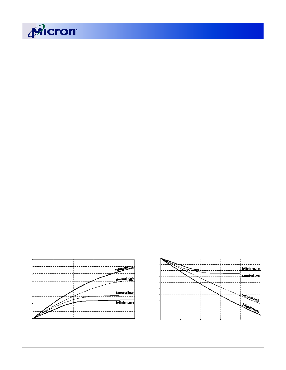
256Mb: x4, x8, x16
DDR SDRAM
09005aef8076894f
Micron Technology, Inc., reserves the right to change products or specifications without notice.
256MBDDRx4x8x16_2.fm - Rev. F 6/03 EN
61
©2003 Micron Technology, Inc.
t
DH for each 0.1 V/ns reduction in slew rate. For -
6, -6T and -6R speed grades, slew rate must be
≥ 0.5 V/ns. If slew rate exceeds 4 V/ns, functional-
ity is uncertain.
32. V
DD
must not vary more than four percent if CKE
is not active while any bank is active.
33. The clock is allowed up to Ī150ps of jitter. Each
timing parameter is allowed to vary by the same
amount.
34.
t
HP (MIN) is the lesser of
t
CL minimum and
t
CH
minimum actually applied to the device CK and
CK# inputs, collectively during bank active.
35. READs and WRITEs with auto precharge are not
allowed to be issued until
t
RAS (MIN) can be satis-
fied prior to the internal PRECHARGE command
being issued.
36. Any positive glitch must be less than 1/3 of the
clock cycle and not more than +400mV or 2.9V,
whichever is less. Any negative glitch must be less
than 1/3 of the clock cycle and not exceed either
-300mV or 2.2V, whichever is more positive.
37. Normal output drive curves:
a. The full variation in driver pull-down current
from minimum to maximum process, temper-
ature, and voltage will lie within the outer
bounding lines of the V-I curve of Figure 36
b. The variation in driver pull-down current
within nominal limits of voltage and tempera-
ture is expected, but not guaranteed, to lie
within the inner bounding lines of the V-I
curve of Figure 36.
c. The full variation in driver pull-up current
from minimum to maximum process, temper-
ature and voltage will lie within the outer
bounding lines of the V-I curve of Figure 37.
d. The variation in driver pull-up current within
nominal limits of voltage and temperature is
expected, but not guaranteed, to lie within the
inner bounding lines of the V-I curve of
Figure 37.
e. The full variation in the ratio of the maximum
to minimum pull-up and pull-down current
should be between 0.71 and 1.4, for device
drain-to-source voltages from 0.1V to 1.0V, and
at the same voltage and temperature. f ) The
full variation in the ratio of the nominal pull-
up to pull-down current should be unity Ī10
percent, for device drain-to-source voltages
from 0.1V to 1.0V.
38. Reduced output drive curves:
a. The full variation in driver pull-down current
from minimum to maximum process, temper-
ature, and voltage will lie within the outer
bounding lines of the V-I curve of Figure 38.
b. The variation in driver pull-down current
within nominal limits of voltage and tempera-
ture is expected, but not guaranteed, to lie
within the inner bounding lines of the V-I
curve of Figure 38.
c. The full variation in driver pull-up current
from minimum to maximum process, temper-
ature and voltage will lie within the outer
bounding lines of the V-I curve of Figure 39.
d. The variation in driver pull-up current within
nominal limits of voltage and temperature is
expected, but not guaranteed, to lie within the
inner bounding lines of the V-I curve of
Figure 39.
Figure 36: Full Drive Pull-Down
Characteristics
Figure 37: Full Drive Pull-Up
Characteristics
0
20
40
60
80
100
120
140
160
0.0
0.5
1.0
1.5
2.0
2.5
V
OUT
(V)
I
OUT
(m
A
)
-200
-180
-160
-140
-120
-100
-80
-60
-40
-20
0
0.0
0.5
1.0
1.5
2.0
2.5
V
DD
Q - V
OUT
(V )
I
OUT
(m
A
)
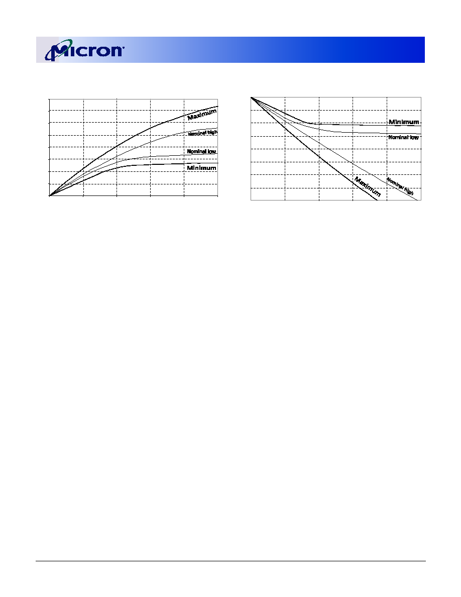
256Mb: x4, x8, x16
DDR SDRAM
09005aef8076894f
Micron Technology, Inc., reserves the right to change products or specifications without notice.
256MBDDRx4x8x16_2.fm - Rev. F 6/03 EN
62
©2003 Micron Technology, Inc.
Figure 38: Reduced Drive Pull-Down
Characteristics
Figure 39: Reduced Drive Pull-Up
Characteristics
e. The full variation in the ratio of the maximum
to minimum pull-up and pull-down current
should be between 0.71 and 1.4 for device
drain-to-source voltages from 0.1V to 1.0V, and
at the same voltage and temperature.
f. The full variation in the ratio of the nominal
pull-up to pull-down current should be unity
Ī10 percent, for device drain-to-source volt-
ages from 0.1V to 1.0V.
39.
The voltage levels used are derived from a mini-
mum
V
DD
level and the referenced test load. In
practice, the voltage levels obtained from a
properly terminated bus will provide signifi-
cantly different voltage values.
40.
V
IH
overshoot: V
IH
(MAX) = V
DD
Q + 1.5V for a
pulse width
£ 3ns and the pulse width can not
be greater than
1/3
of the cycle rate. V
IL
under-
shoot: V
IL
(MIN) = -1.5V for a pulse width
£ 3ns
and the pulse width can not be greater than
1/3
of the cycle rate.
41. V
DD
and V
DD
Q must track each other.
42. This maximum value is derived from the refer-
enced test load. In practice, the values obtained in
a typical terminated design may reflect up to
310ps less for
t
HZ (MAX) and the last DVW.
t
HZ
(MAX) will prevail over
t
DQSCK (MAX) +
t
RPST
(MAX) condition.
t
LZ (MIN) will prevail over
t
DQSCK (MIN) +
t
RPRE (MAX) condition.
43. For slew rates of greater than 1 V/ns the (LZ) tran-
sition will start about 310ps earlier.
44. During initialization, V
DD
Q, V
TT
, and V
REF
must be
equal to or less than V
DD
+ 0.3V. Alternatively, V
TT
may be 1.35V maximum during power-up, even if
V
DD
/V
DD
Q are 0V, provided a minimum of 42
W of
series resistance is used between the V
TT
supply
and the input pin.
45. The current Micron part operates below the slow-
est JEDEC operating frequency of 83 MHz. As
such, future die may not reflect this option.
46. For the -6R speed grade, the minimum allowed
V
DD
and V
DD
Q is 2.4V.
47. When an input signal is indicated to be HIGH or
LOW, it is defined as a steady state logic HIGH or
LOW.
48. Random addressing changing; 50 percent of data
changing at every transfer.
49. Random addressing changing; 100 percent of data
changing at every transfer.
50. CKE must be active (HIGH) during the entire time
a refresh command is executed. That is, from the
time the AUTO REFRESH command is registered,
CKE must be active at each rising clock edge, until
t
RFC has been satisfied.
51. I
DD
2N specifies the DQ, DQS and DM to be driven
to a valid HIGH or LOW logic level. I
DD
2Q is simi-
lar to I
DD
2F except I
DD
2Q specifies the address
and control inputs to remain stable. Although
I
DD
2F, I
DD
2N, and I
DD
2Q are similar, I
DD
2F is
"worst case."
52. Whenever the operating frequency is altered, not
including jitter, the DLL is required to be reset fol-
lowed by 200 clock cycles before any READ com-
mand.
0
10
20
30
40
50
60
70
80
0.0
0.5
1.0
1.5
2.
V
OUT
(V)
I
OU
T
(m
A
)
-80
-70
-60
-50
-40
-30
-20
-10
0
0.0
0.5
1.0
1.5
2.0
2.5
V
DD
Q - V
OUT
(V)
I
OU
T
(m
A
)
256Mb: x4, x8, x16
DDR SDRAM
09005aef8076894f
Micron Technology, Inc., reserves the right to change products or specifications without notice.
256MBDDRx4x8x16_2.fm - Rev. F 6/03 EN
63
©2003 Micron Technology, Inc.
NOTE:
The above characteristics are specified under best, worst, and nominal process variations/conditions.
Table 27: Normal Output Drive Characteristics
VOLTAGE
(V)
PULL-DOWN CURRENT (mA)
PULL-UP CURRENT (mA)
NOMINAL
LOW
NOMINAL
HIGH
MINIMUM
MAXIMUM
NOMINAL
LOW
NOMINAL
HIGH
MINIMUM
MAXIMUM
0.1
6.0
6.8
4.6
9.6
-6.1
-7.6
-4.6
-10.0
0.2
12.2
13.5
9.2
18.2
-12.2
-14.5
-9.2
-20.0
0.3
18.1
20.1
13.8
26.0
-18.1
-21.2
-13.8
-29.8
0.4
24.1
26.6
18.4
33.9
-24.0
-27.7
-18.4
-38.8
0.5
29.8
33.0
23.0
41.8
-29.8
-34.1
-23.0
-46.8
0.6
34.6
39.1
27.7
49.4
-34.3
-40.5
-27.7
-54.4
0.7
39.4
44.2
32.2
56.8
-38.1
-46.9
-32.2
-61.8
0.8
43.7
49.8
36.8
63.2
-41.1
-53.1
-36.0
-69.5
0.9
47.5
55.2
39.6
69.9
-43.8
-59.4
-38.2
-77.3
1.0
51.3
60.3
42.6
76.3
-46.0
-65.5
-38.7
-85.2
1.1
54.1
65.2
44.8
82.5
-47.8
-71.6
-39.0
-93.0
1.2
56.2
69.9
46.2
88.3
-49.2
-77.6
-39.2
-100.6
1.3
57.9
74.2
47.1
93.8
-50.0
-83.6
-39.4
-108.1
1.4
59.3
78.4
47.4
99.1
-50.5
-89.7
-39.6
-115.5
1.5
60.1
82.3
47.7
103.8
-50.7
-95.5
-39.9
-123.0
1.6
60.5
85.9
48.0
108.4
-51.0
-101.3
-40.1
-130.4
1.7
61.0
89.1
48.4
112.1
-51.1
-107.1
-40.2
-136.7
1.8
61.5
92.2
48.9
115.9
-51.3
-112.4
-40.3
-144.2
1.9
62.0
95.3
49.1
119.6
-51.5
-118.7
-40.4
-150.5
2.0
62.5
97.2
49.4
123.3
-51.6
-124.0
-40.5
-156.9
2.1
62.8
99.1
49.6
126.5
-51.8
-129.3
-40.6
-163.2
2.2
63.3
100.9
49.8
129.5
-52.0
-134.6
-40.7
-169.6
2.3
63.8
101.9
49.9
132.4
-52.2
-139.9
-40.8
-176.0
2.4
64.1
102.8
50.0
135.0
-52.3
-145.2
-40.9
-181.3
2.5
64.6
103.8
50.2
137.3
-52.5
-150.5
-41.0
-187.6
2.6
64.8
104.6
50.4
139.2
-52.7
-155.3
-41.1
-192.9
2.7
65.0
105.4
50.5
140.8
-52.8
-160.1
-41.2
-198.2

256Mb: x4, x8, x16
DDR SDRAM
09005aef8076894f
Micron Technology, Inc., reserves the right to change products or specifications without notice.
256MBDDRx4x8x16_2.fm - Rev. F 6/03 EN
64
©2003 Micron Technology, Inc.
NOTE:
The above characteristics are specified under best, worst, and nominal process variations/conditions.
Table 28: Reduced Output Drive Characteristics
VOLTAGE
(V)
PULL-DOWN CURRENT (mA)
PULL-UP CURRENT (mA)
NOMINAL
LOW
NOMINAL
HIGH
MINIMUM
MAXIMUM
NOMINAL
LOW
NOMINAL
HIGH
MINIMUM
MAXIMUM
0.1
3.4
3.8
2.6
5.0
-3.5
-4.3
-2.6
-5.0
0.2
6.9
7.6
5.2
9.9
-6.9
-7.8
-5.2
-9.9
0.3
10.3
11.4
7.8
14.6
-10.3
-12.0
-7.8
-14.6
0.4
13.6
15.1
10.4
19.2
-13.6
-15.7
-10.4
-19.2
0.5
16.9
18.7
13.0
23.6
-16.9
-19.3
-13.0
-23.6
0.6
19.9
22.1
15.7
28.0
-19.4
-22.9
-15.7
-28.0
0.7
22.3
25.0
18.2
32.2
-21.5
-26.5
-18.2
-32.2
0.8
24.7
28.2
20.8
35.8
-23.3
-30.1
-20.4
-35.8
0.9
26.9
31.3
22.4
39.5
-24.8
-33.6
-21.6
-39.5
1.0
29.0
34.1
24.1
43.2
-26.0
-37.1
-21.9
-43.2
1.1
30.6
36.9
25.4
46.7
-27.1
-40.3
-22.1
-46.7
1.2
31.8
39.5
26.2
50.0
-27.8
-43.1
-22.2
-50.0
1.3
32.8
42.0
26.6
53.1
-28.3
-45.8
-22.3
-53.1
1.4
33.5
44.4
26.8
56.1
-28.6
-48.4
-22.4
-56.1
1.5
34.0
46.6
27.0
58.7
-28.7
-50.7
-22.6
-58.7
1.6
34.3
48.6
27.2
61.4
-28.9
-52.9
-22.7
-61.4
1.7
34.5
50.5
27.4
63.5
-28.9
-55.0
-22.7
-63.5
1.8
34.8
52.2
27.7
65.6
-29.0
-56.8
-22.8
-65.6
1.9
35.1
53.9
27.8
67.7
-29.2
-58.7
-22.9
-67.7
2.0
35.4
55.0
28.0
69.8
-29.2
-60.0
-22.9
-69.8
2.1
35.6
56.1
28.1
71.6
-29.3
-61.2
-23.0
-71.6
2.2
35.8
57.1
28.2
73.3
-29.5
-62.4
-23.0
-73.3
2.3
36.1
57.7
28.3
74.9
-29.5
-63.1
-23.1
-74.9
2.4
36.3
58.2
28.3
76.4
-29.6
-63.8
-23.2
-76.4
2.5
36.5
58.7
28.4
77.7
-29.7
-64.4
-23.2
-77.7
2.6
36.7
59.2
28.5
78.8
-29.8
-65.1
-23.3
-78.8
2.7
36.8
59.6
28.6
79.7
-29.9
-65.8
-23.3
-79.7
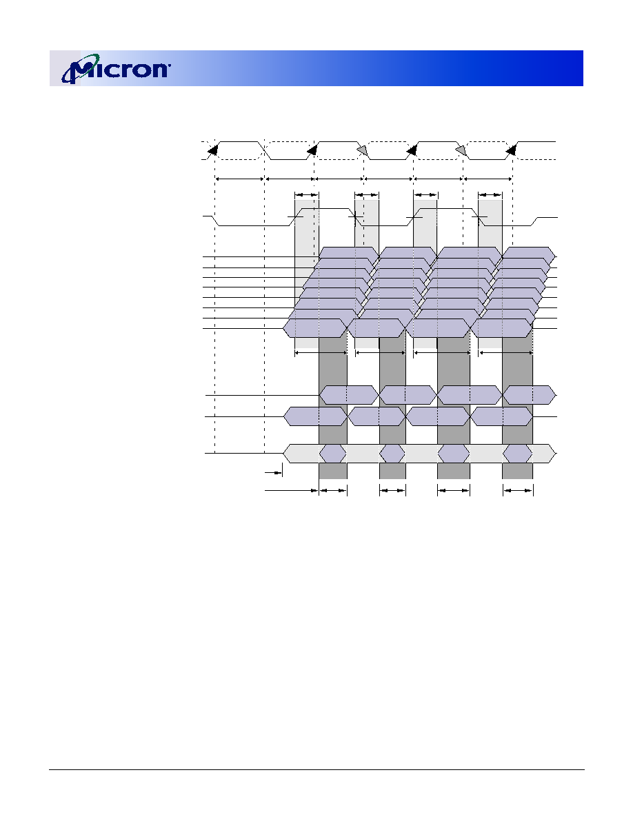
256Mb: x4, x8, x16
DDR SDRAM
09005aef8076894f
Micron Technology, Inc., reserves the right to change products or specifications without notice.
256MBDDRx4x8x16_2.fm - Rev. F 6/03 EN
65
©2003 Micron Technology, Inc.
Figure 40: x4, x8 Data Output Timing ≠
t
DQSQ,
t
QH, and Data Valid Window
NOTE:
1. DQ transitioning after DQS transition define
t
DQSQ window. DQS transitions at T2 and at T2n are "early DQS," at T3,
"nominal DQS," and at T3n, "late DQS."
2. For a x4, only two DQ apply.
3.
t
DQSQ is derived at each DQS clock edge and is not cumulative over time and begins with DQS transition and ends with
the last valid DQ transition.
4.
t
QH is derived from
t
HP:
t
QH =
t
HP -
t
QHS.
5.
t
HP is the lesser of
t
CL or
t
CH clock transition collectively when a bank is active.
6. The data valid window is derived for each DQS transitions and is defined as
t
QH minus
t
DQSQ.
DQ (Last data valid)
DQ
2
DQ
2
DQ
2
DQ
2
DQ
2
DQ
2
DQS
1
DQ (Last data valid)
DQ (First data no longer valid)
DQ (First data no longer valid)
All DQ and DQS, collectively
6
Earliest signal transition
Latest signal transition
T2
T2
T2
T2n
T2n
T2n
T3
T3
T3
T3n
T3n
T3n
CK
CK#
T1
T2
T3
T4
T2n
T3n
tQH
4
tHP
5
tHP
5
tHP
5
tQH
4
tQH
4
tHP
5
tHP
5
tHP
5
tQH
4
tDQSQ
3
tDQSQ
3
tDQSQ
3
tDQSQ
3
Data
Valid
window
Data
Valid
window
Data
Valid
window
Data
Valid
window
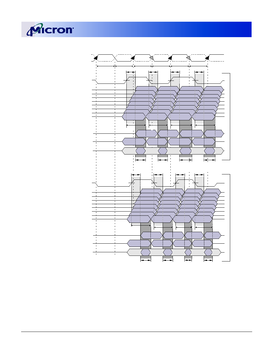
256Mb: x4, x8, x16
DDR SDRAM
09005aef8076894f
Micron Technology, Inc., reserves the right to change products or specifications without notice.
256MBDDRx4x8x16_2.fm - Rev. F 6/03 EN
66
©2003 Micron Technology, Inc.
Figure 41: x16 Data Output Timing ≠
t
DQSQ,
t
QH, and Data Valid Window
NOTE:
1. DQ transitioning after DQS transition define
t
DQSQ window. LDQS defines the lower byte and UDQS defines the upper
byte.
2. DQ0, DQ1, DQ2, DQ3, DQ4, DQ5, DQ6, or DQ7.
3.
t
DQSQ is derived at each DQS clock edge and is not cumulative over time and begins with DQS transition and ends with
the last valid DQ transition.
4.
t
QH is derived from
t
HP:
t
QH =
t
HP -
t
QHS.
5.
t
HP is the lesser of
t
CL or
t
CH clock transition collectively when a bank is active.
6. The data valid window is derived for each DQS transition and is
t
QH minus
t
DQSQ.
7. DQ8, DQ9, DQ10, D11, DQ12, DQ13, DQ14, or DQ15.
DQ (Last data valid)
2
DQ
2
DQ
2
DQ
2
DQ
2
DQ
2
DQ
2
LDQS
1
DQ (Last data valid)
2
DQ (First data no longer valid)
2
DQ (First data no longer valid)
2
DQ0 - DQ7 and LDQS, collectively
6
T2
T2
T2
T2n
T2n
T2n
T3
T3
T3
T3n
T3n
T3n
CK
CK#
T1
T2
T3
T4
T2n
T3n
tQH
4
tQH
4
tDQSQ
3
tDQSQ
3
tDQSQ
3
tDQSQ
3
Data Valid
window
Data Valid
window
DQ (Last data valid)
7
DQ
7
DQ
7
DQ
7
DQ
7
DQ
7
DQ
7
UDQS
1
DQ (Last data valid)
7
DQ (First data no longer valid)
7
DQ (First data no longer valid)
7
DQ8 - DQ15 and UDQS, collectively
6
T2
T2
T2
T2n
T2n
T2n
T3
T3
T3
T3n
T3n
T3n
tQH
4
tQH
4
tQH
4
tQH
4
tDQSQ
3
tDQSQ
3
tDQSQ
3
tDQSQ
3
tHP
5
tHP
5
tHP
5
tHP
5
tHP
5
tHP
5
tQH
4
tQH
4
Data Valid
window
Data Valid
window
Data Valid
window
Data Valid
window
Data Valid
window
Upper Byte
Lower Byte
Data Valid
window

256Mb: x4, x8, x16
DDR SDRAM
09005aef8076894f
Micron Technology, Inc., reserves the right to change products or specifications without notice.
256MBDDRx4x8x16_2.fm - Rev. F 6/03 EN
67
©2003 Micron Technology, Inc.
Figure 42: Data Output Timing ≠
t
AC and
t
DQSCK
NOTE:
1.
t
DQSCK is the DQS output window relative to CK and is the "long-term" component of DQS skew.
2. DQ transitioning after DQS transition define
t
DQSQ window.
3. All DQ must transition by
t
DQSQ after DQS transitions, regardless of
t
AC.
4.
t
AC is the DQ output window relative to CK, and is the "long-term" component of DQ skew.
5.
t
LZ (MIN) and
t
AC (MIN) are the first valid signal transition.
6.
t
HZ (MAX),and
t
AC (MAX) are the latest valid signal transition.
7. READ command with CL = 2 issued at T0.
CK
CK#
DQS, or LDQS/UDQS
2
T0
7
T1
T2
T3
T4
T5
T2n
T3n
T4n
T5n
T6
tRPST
tLZ (MIN)
tDQSCK
1
(MAX)
tDQSCK
1
(MIN)
tDQSCK
1
(MAX)
tDQSCK
1
(MIN)
tHZ(MAX)
tRPRE
DQ (Last data valid)
DQ (First data valid)
All DQ values, collectively
3
tAC
4
(MIN)
tAC
4
(MAX)
tLZ (MIN)
tHZ (MAX)
T2
T2
T2n
T3n
T4n
T5n
T2n
T2n
T3n
T3n
T4n
T4n
T5n
T5n
T3
T4
T4
T5
T5
T2
T3
T4
T5
T3
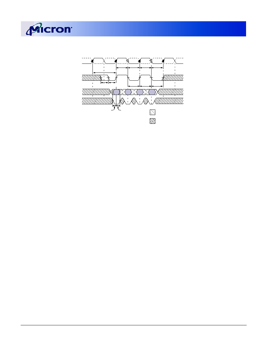
256Mb: x4, x8, x16
DDR SDRAM
09005aef8076894f
Micron Technology, Inc., reserves the right to change products or specifications without notice.
256MBDDRx4x8x16_2.fm - Rev. F 6/03 EN
68
©2003 Micron Technology, Inc.
Figure 43: Data Input Timing
NOTE:
1.
t
DSH (MIN) generally occurs during
t
DQSS (MIN).
2.
t
DSS (MIN) generally occurs during
t
DQSS (MAX).
3. WRITE command issued at T0.
4. For x16, LDQS controls the lower byte and UDQS controls the upper byte.
DQS
tDQSS
tDQSH tWPST
tDH
tDS
tDQSL
tDSS2 tDSH1
tDSH1
tDSS2
DM
DQ
CK
CK#
T0
3
T1
T1n
T2
T2n
T3
DI
b
DON'T CARE
TRANSITIONING DATA
tWPRE
tWPRES
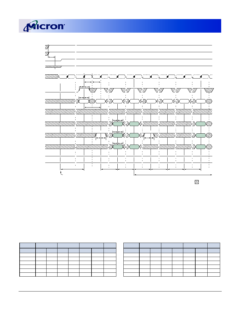
256Mb: x4, x8, x16
DDR SDRAM
09005aef8076894f
Micron Technology, Inc., reserves the right to change products or specifications without notice.
256MBDDRx4x8x16_2.fm - Rev. F 6/03 EN
69
©2003 Micron Technology, Inc.
Figure 44: Initialize and Load Mode Registers
NOTE:
1. V
TT
is not applied directly to the device; however,
t
VTD should be greater than or equal to zero to avoid device latch-up. V
DD
Q, V
TT
, and V
REF
must be equal to or less than V
DD
+ 0.3V. Alternatively, V
TT
may be 1.35V maximum during power-up, even if V
DD
/V
DD
Q are 0V, provided a
minimum of 42
W of series resistance is used between the V
TT
supply and the input pin. Once initialized, V
REF
must always be powered within
the specified range.
2. Reset the DLL with A8 = H while programming the operating parameters.
3.
t
MRD is required before any command can be applied, and 200 cycles of CK are required before a READ command can be issued.
4. The two AUTO REFRESH commands at Td0 and Te0 may be applied prior to the LOAD MODE REGISTER (LMR) command at Ta0.
5. Although not required by the Micron device, JEDEC specifies issuing another LMR command (A8 = L) prior to activating any
bank. If another LMR command is issued, the same operating parameters must be used as previously issued.
6. PRE = PRECHARGE command; LMR = LOAD MODE REGISTER command; AR = AUTO REFRESH command; ACT = ACTIVE com-
mand; RA = Row Address; and BA = Bank Address.
t
VTD
1
CKE
LVCMOS
LOW LEVEL
DQ
BA0, BA1
200 cycles of CK
3
Load Extended
Mode Register
Load Mode
Register
2
tMRD
tMRD
tRP
tRFC
tRFC
5
t
IS
Power-up: V
DD
and CK stable
T = 200Ķs
High-Z
t
IH
DM
DQS
High-Z
A0-A9,
A11, A12
RA
A10
RA
ALL BANKS
CK
CK#
t
CH
t
CL
t
CK
V
TT
1
V
REF
V
DD
V
DD
Q
COMMAND
6
LMR
NOP
PRE
LMR
AR
AR
ACT5
tIS tIH
BA0 = H,
BA1 = L
tIS
tIH
t
IS
t
IH
BA0 = L,
BA1 = L
tIS
tIH
(
)
(
)
(
)
(
)
(
)
(
)
(
)
(
)
CODE CODE
tIS
tIH
CODE CODE
PRE
ALL BANKS
tIS
tIH
T0
T1
Ta0
Tb0
Tc0
Td0
Te0
Tf0
(
)
(
)
DON'T CARE
BA
(
)
(
)
(
)
(
)
(
)
(
)
(
)
(
)
(
)
(
)
(
)
(
)
(
)
(
)
(
)
(
)
(
)
(
)
(
)
(
)
(
)
(
)
(
)
(
)
(
)
(
)
(
)
(
)
tRP
(
)
(
)
(
)
(
)
(
)
(
)
(
)
(
)
(
)
(
)
(
)
(
)
(
)
(
)
(
)
(
)
(
)
(
)
(
)
(
)
(
)
(
)
(
)
(
)
(
)
(
)
(
)
(
)
(
)
(
)
(
)
(
)
(
)
(
)
(
)
(
)
(
)
(
)
(
)
(
)
(
)
(
)
(
)
(
)
(
)
(
)
(
)
(
)
(
)
(
)
(
)
(
)
(
)
(
)
(
)
(
)
(
)
(
)
(
)
(
)
(
)
(
)
(
)
(
)
(
)
(
)
(
)
(
)
(
)
(
)
(
)
(
)
(
)
(
)
(
)
(
)
(
)
(
)
(
)
(
)
(
)
(
)
(
)
(
)
(
)
(
)
(
)
(
)
(
)
(
)
(
)
(
)
(
)
(
)
(
)
(
)
(
)
(
)
(
)
(
)
(
)
(
)
(
)
(
)
(
)
(
)
(
)
(
)
(
)
(
)
(
)
(
)
(
)
(
)
(
)
(
)
(
)
(
)
(
)
(
)
(
)
(
)
(
)
(
)
(
)
(
)
(
)
(
)
(
)
(
)
(
)
(
)
(
)
(
)
(
)
(
)
(
)
(
)
(
)
(
)
(
)
(
)
(
)
(
)
(
)
(
)
(
)
(
)
(
)
(
)
(
)
(
)
(
)
(
)
(
)
(
)
(
)
(
)
(
)
(
)
(
)
(
)
(
)
(
)
(
)
(
)
(
)
(
)
(
)
(
)
(
)
(
)
(
)
(
)
(
)
(
)
(
)
(
)
(
)
(
)
(
)
(
)
(
)
(
)
(
)
(
)
(
)
(
)
(
)
(
)
(
)
(
)
-6/6T/6T
-75E/75Z
-75
SYMBOL
MIN
MAX
MIN
MAX
MIN
MAX
UNITS
t
CH
0.45
0.55
0.45
0.55
0.45
0.55
t
CK
t
CL
0.45
0.55
0.45
0.55
0.45
0.55
t
CK
t
CK (2.5)
6
13
7.5
13
7.5
13
ns
t
CK (2)
7.5
13
7.5
13
10
13
ns
t
IH
F
.75
.90
0.90
ns
t
IS
F
.75
.90
0.90
ns
t
IH
S
0.8
1
1
ns
t
IS
S
0.8
1
1
ns
t
MRD
15
15
15
ns
t
RFC
72
75
75
ns
t
RP
18
15
20
ns
t
VTD
0
0
0
ns
-6/6T/6T
-75E/75Z
-75
SYMBOL
MIN
MAX
MIN
MAX
MIN
MAX
UNITS
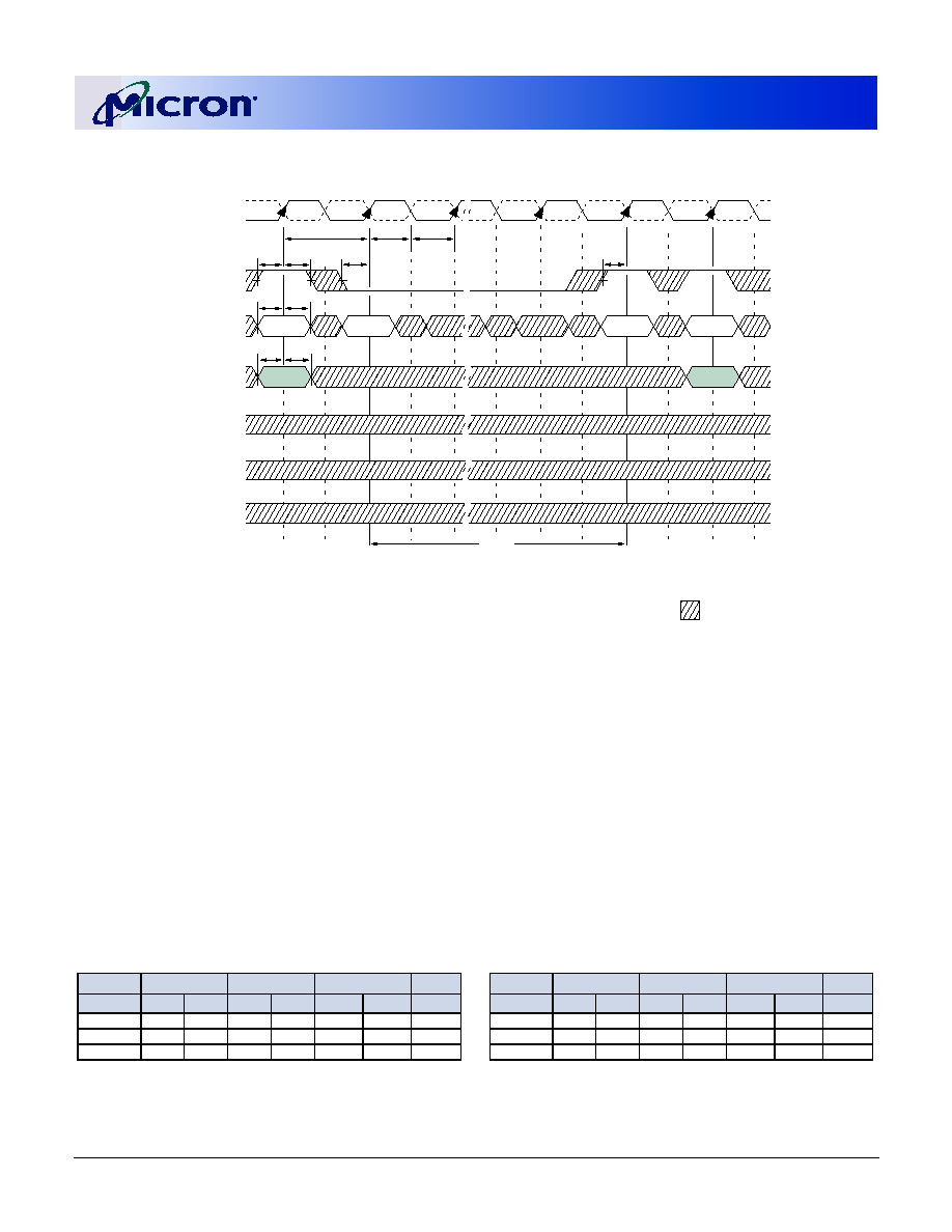
256Mb: x4, x8, x16
DDR SDRAM
09005aef8076894f
Micron Technology, Inc., reserves the right to change products or specifications without notice.
256MBDDRx4x8x16_2.fm - Rev. F 6/03 EN
70
©2003 Micron Technology, Inc.
Figure 45: Power-Down Mode
NOTE:
1. Once initialized, V
REF
must always be powered within the specified range.
2. If this command is a PRECHARGE (or if the device is already in the idle state), then the power-down mode shown is pre-
charge power-down. If this command is an ACTIVE (or if at least one row is already active), then the power-down mode
shown is active power-down.
3. No column accesses are allowed to be in progress at the time power-down is entered.
CK
CK#
COMMAND
VALID2
NOP
ADDR
CKE
1
DQ
DM
DQS
VALID
t
CK
t
CH
t
CL
t
IS
t
IS
t
IH
t
IS
t
IS
t
IH
t
IH
t
IS
Enter
3
Power-Down
Mode
Exit
Power-Down
Mode
t
REFC
(
)
(
)
(
)
(
)
(
)
(
)
(
)
(
)
(
)
(
)
(
)
(
)
(
)
(
)
(
)
(
)
(
)
(
)
(
)
(
)
(
)
(
)
T0
T1
Ta0
Ta1
Ta2
T2
NOP
DON'T CARE
(
)
(
)
(
)
(
)
VALID
VALID
-6/6T/6T
-75E/75Z
-75
SYMBOL
MIN
MAX
MIN
MAX
MIN
MAX
UNITS
t
CH
0.45
0.55
0.45
0.55
0.45
0.55
t
CK
t
CL
0.45
0.55
0.45
0.55
0.45
0.55
t
CK
t
CK (2.5)
6
13
7.5
13
7.5
13
ns
t
CK (2)
7.5
13
7.5
13
10
13
ns
t
IH
S
0.8
1
1
ns
t
IS
S
0.8
1
1
ns
-6/6T/6T
-75E/75Z
-75
SYMBOL
MIN
MAX
MIN
MAX
MIN
MAX
UNITS

256Mb: x4, x8, x16
DDR SDRAM
09005aef8076894f
Micron Technology, Inc., reserves the right to change products or specifications without notice.
256MBDDRx4x8x16_2.fm - Rev. F 6/03 EN
71
©2003 Micron Technology, Inc.
Figure 46: Auto Refresh Mode
NOTE:
1. PRE = PRECHARGE; ACT = ACTIVE; AR = AUTO REFRESH; RA = Row Address; and BA = Bank Address.
2. NOP commands are shown for ease of illustration; other valid commands may be possible at these times. CKE must be
active during clock positive transitions.
3. NOP or COMMAND INHIBIT are the only commands allowed until after
t
RFC time; CKE must be active during clock posi-
tive transitions.
4. "Don't Care" if A10 is HIGH at this point; A10 must be HIGH if more than one bank is active (i.e., must precharge all
active banks).
5. DM, DQ, and DQS signals are all "Don't Care"/High-Z for operations shown.
6. The second AUTO REFRESH is not required and is only shown as an example of two back-to-back AUTO REFRESH com-
mands.
CK
CK#
COMMAND
1
NOP2
VALID
VALID
NOP 2
NOP2
PRE
CKE
RA
A0-A9,
A11, A12
1
A10
1
BA0, BA1
1
Bank(s)4
BA
AR
NOP2, 3
AR6
NOP2, 3
ACT
NOP2
ONE BANK
ALL BANKS
CK
t
CH
t
CL
t
IS
t
IS
t
IH
t
IH
t
IS
t
IH
RA
DQ
5
DM
5
DQS
5
tRFC5
tRP
tRFC
T0
T1
T2
T3
T4
Ta0
Tb0
Ta1
Tb1
Tb2
DON'T CARE
(
)
(
)
(
)
(
)
(
)
(
)
(
)
(
)
(
)
(
)
(
)
(
)
(
)
(
)
(
)
(
)
(
)
(
)
(
)
(
)
(
)
(
)
(
)
(
)
(
)
(
)
(
)
(
)
(
)
(
)
(
)
(
)
(
)
(
)
(
)
(
)
(
)
(
)
(
)
(
)
(
)
(
)
(
)
(
)
(
)
(
)
(
)
(
)
(
)
(
)
(
)
(
)
(
)
(
)
(
)
(
)
(
)
(
)
(
)
(
)
(
)
(
)
(
)
(
)
(
)
(
)
(
)
(
)
(
)
(
)
(
)
(
)
-6/6T/6T
-75E/75Z
-75
SYMBOL
MIN
MAX
MIN
MAX
MIN
MAX
UNITS
t
CH
0.45
0.55
0.45
0.55
0.45
0.55
t
CK
t
CL
0.45
0.55
0.45
0.55
0.45
0.55
t
CK
t
CK (2.5)
6
13
7.5
13
7.5
13
ns
t
CK (2)
7.5
13
7.5
13
10
13
ns
t
IH
F
0.75
0.90
0.90
ns
t
IS
F
0.75
0.90
0.90
ns
t
IH
S
0.8
1
1
ns
t
IS
S
0.8
1
1
ns
t
RFC
72
75
75
ns
t
RP
18
15
20
ns
-6/6T/6T
-75E/75Z
-75
SYMBOL
MIN
MAX
MIN
MAX
MIN
MAX
UNITS
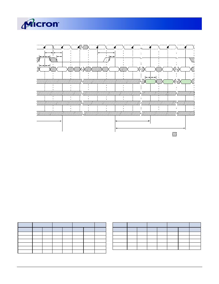
256Mb: x4, x8, x16
DDR SDRAM
09005aef8076894f
Micron Technology, Inc., reserves the right to change products or specifications without notice.
256MBDDRx4x8x16_2.fm - Rev. F 6/03 EN
72
©2003 Micron Technology, Inc.
Figure 47: Self Refresh Mode
NOTE:
1. Clock must be stable until after the SELF REFRESH command has been registered. A change in clock frequency is allowed before
Ta0, provided it is within the specified tCK limits. Regardless, the clock must be stable before exiting self refresh mode. That is,
the clock must be cycling within specifications by Ta0.
2. NOPs are interchangeable with DESELECT commands; AR = AUTO REFRESH command.
3. Auto refresh is not required at this point, but is highly recommended.
4. Device must be in the all banks idle state prior to entering self refresh mode.
5.
t
XSNR is required before any non-READ command can be applied; only NOP or DESELECT commands are allowed until Tb1.
6.
t
XSRD (200 cycles of a valid CK and CKE = high) is required before any READ command can be applied.
7. As a general rule, any time self refresh mode is exited, the DRAM may not re-enter the self refresh mode until all rows have
been refreshed via the AUTO REFRESH command at the distributed refresh rate,
t
REFI, or faster. However, self refresh mode
may be re-entered anytime after exiting, if the following conditions are all met:
a.
The DRAM had been in the Self Refresh Mode for a minimum of 200ms prior to exiting.
b.
t
XSNR and
t
XSRD are not violated.
c.
At least two AUTO REFRESH commands are performed during each tREFI interval while the DRAM remains out of
Self Refresh mode.
8. If the clock frequency is changed during self refresh mode, a DLL reset is required upon exit.
9. Once initialized, V
REF
must always be powered within the specified range.
CK
1
CK#
COMMAND
2
NOP
AR
ADDR
CKE
DQ
DM
DQS
NOP
t
RP
4
t
CH
t
CL
tCK
t
IS
t
IS
t
IH
t
IS
t
IH
tIS
Enter Self Refresh Mode
7
Exit Self Refresh Mode
7
T0
T1
1
Ta1
(
)
(
)
DON'T CARE
Ta0
1
t
XSRD
6
(
)
(
)
(
)
(
)
(
)
(
)
(
)
(
)
NOP
VALID3
VALID
(
)
(
)
(
)
(
)
(
)
(
)
(
)
(
)
(
)
(
)
(
)
(
)
(
)
(
)
(
)
(
)
(
)
(
)
(
)
(
)
tXSNR
5
(
)
(
)
(
)
(
)
(
)
(
)
(
)
(
)
(
)
(
)
(
)
(
)
(
)
(
)
(
)
(
)
(
)
(
)
(
)
(
)
(
)
(
)
(
)
(
)
(
)
(
)
(
)
(
)
(
)
(
)
(
)
(
)
(
)
(
)
(
)
(
)
(
)
(
)
(
)
(
)
(
)
(
)
(
)
(
)
Ta2
Tb1
Tb2
Tc1
VALID
VALID
VALID
t
IS
t
IH
(
)
(
)
(
)
(
)
VALID
(
)
(
)
(
)
(
)
-6/6T/6T
-75E/75Z
-75
SYMBOL
MIN
MAX
MIN
MAX
MIN
MAX
UNITS
t
CH
0.45
0.55
0.45
0.55
0.45
0.55
t
CK
t
CL
0.45
0.55
0.45
0.55
0.45
0.55
t
CK
t
CK (2.5)
6
13
7.5
13
7.5
13
ns
t
CK (2)
7.5
13
7.5
13
10
13
ns
t
IH
F
0.75
0.90
0.90
ns
t
IS
F
0.75
0.90
0.90
ns
t
IH
S
0.8
1
1
ns
t
IS
S
0.8
1
1
ns
t
RFC
72
75
75
ns
t
RP
18
15
20
ns
t
VTD
0
0
0
ns
-6/6T/6T
-75E/75Z
-75
SYMBOL
MIN
MAX
MIN
MAX
MIN
MAX
UNITS

256Mb: x4, x8, x16
DDR SDRAM
09005aef8076894f
Micron Technology, Inc., reserves the right to change products or specifications without notice.
256MBDDRx4x8x16_2.fm - Rev. F 6/03 EN
73
©2003 Micron Technology, Inc.
Figure 48: Bank Read - Without Auto Precharge
NOTE:
1. DOn = data-out from column n; subsequent elements are provided in the programmed order.
2. Burst length = 4 in the case shown.
3. Disable auto precharge.
4. "Don't Care" if A10 is HIGH at T5.
5. PRE = PRECHARGE; ACT = ACTIVE; RA = Row Address; and BA = Bank Address.
6. NOP commands are shown for ease of illustration; other commands may be valid at these times.
7. The PRECHARGE command can only be applied at T5 if
t
RAS minimum is met.
8. Refer to Figure 40 on page 65, Figure 41 on page 66, and Figure 42 on page 67 for detailed DQS and DQ timing.
CK
CK#
CKE
A10
BA0, BA1
t
CK
t
CH
t
CL
t
IS
t
IS
t
IH
t
IS
t
IS
t
IH
t
IH
t
IH
t
IS
t
IH
RA
t
RCD
t
RAS7
t
RC
t
RP
CL = 2
DM
T0
T1
T2
T3
T4
T5
T5n
T6n
T6
T7
T8
DQ
1
DQS
Case 1:
t
AC (MIN) and
t
DQSCK (MIN)
Case 2:
t
AC (MAX) and
t
DQSCK (MAX)
DQ
1
DQS
t
RPRE
t
RPRE
t
RPST
t
RPST
t
DQSCK (MIN)
t
DQSCK
(MAX)
t
LZ (MIN)
t
AC (MIN)
t
LZ (MIN)
DO
n
t
HZ (MAX)
t
AC (MAX)
DO
n
NOP6
NOP6
COMMAND
5
3
ACT
RA
RA
Col n
READ2
PRE
7
Bank x
RA
RA
RA
Bank x
Bank x4
ACT
Bank x
NOP6
NOP6
NOP6
ONE BANK
ALL BANKS
DON'T CARE
TRANSITIONING DATA
x4: A0-A9, A11
x8: A0-A9
x16: A0-A8
x4: A12
x8: A11, A12
x16: A9, A11, A12
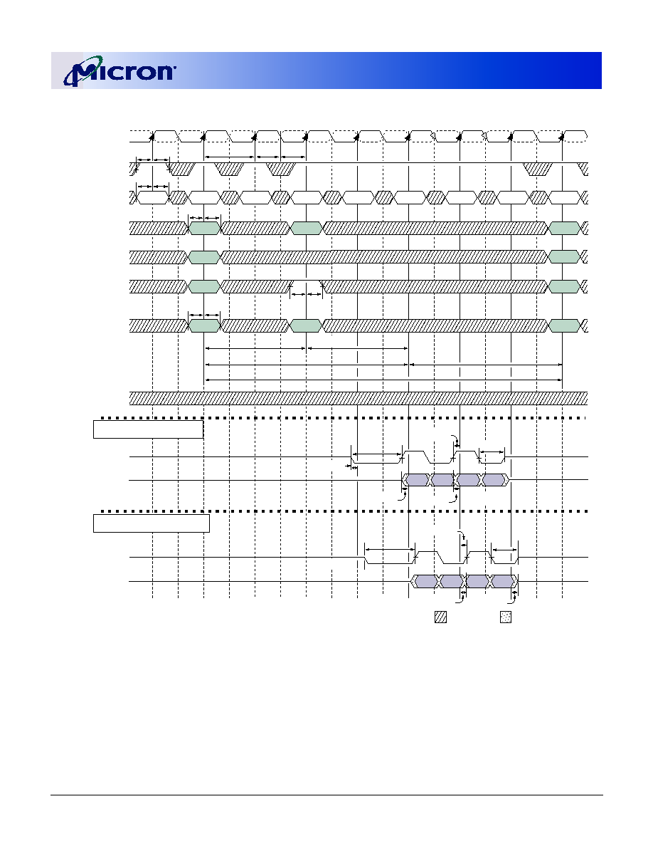
256Mb: x4, x8, x16
DDR SDRAM
09005aef8076894f
Micron Technology, Inc., reserves the right to change products or specifications without notice.
256MBDDRx4x8x16_2.fm - Rev. F 6/03 EN
74
©2003 Micron Technology, Inc.
Figure 49: Bank Read - With Auto Precharge
NOTE:
1. DOn = data-out from column n; subsequent elements are provided in the programmed order.
2. Burst length = 4 in the case shown.
3. Enable auto precharge.
4. ACT = ACTIVE; RA = Row Address; and BA = Bank Address.
5. NOP commands are shown for ease of illustration; other commands may be valid at these times.
6. The READ command can only be applied at T3 if
t
RAP is satisfied at T3.
7.
t
RP starts only after
t
RAS has been satisfied.
8. Refer to Figure 40 on page 65, Figure 41 on page 66, and Figure 42 on page 67 for detailed DQS and DQ timing.
CK
CK#
CKE
A10
BA0, BA1
t
CK
t
CH
t
CL
t
IS
t
IS
t
IH
t
IS
t
IS
t
IH
t
IH
t
IH
IS
IH
RA
t
RC
t
RP7
CL = 2
DM
T0
T1
T2
T3
T4
T5
T5n
T6n
T6
T7
T8
DQ
1
DQS
Case 1:
t
AC (MIN) and
t
DQSCK (MIN)
Case 2:
t
AC (MAX)
and
t
DQSCK (MAX)
DQ
1
DQS
t
RPRE
t
RPRE
t
RPST
t
RPST
t
DQSCK (MIN)
t
DQSCK (MAX)
t
AC (MIN)
t
LZ (MIN)
DO
n
t
HZ (MAX)
t
AC (MAX)
DO
n
NOP5
NOP5
COMMAND
4
3
ACT
RA
RA
Col n
READ2,6
NOP5
Bank x
RA
RA
RA
Bank x
ACT
Bank x
NOP5
NOP5
NOP5
DON'T CARE
TRANSITIONING DATA
x4: A0-A9, A11
x8: A0-A9
x16: A0-A8
x4: A12
x8: A11, A12
x16: A9, A11, A12
t
RAS
t
LZ
(MIN)
t
RCD,
t
RAP6
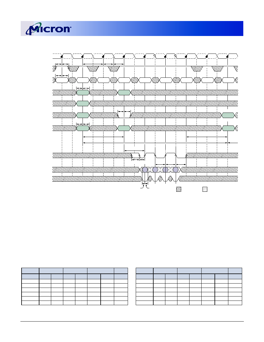
256Mb: x4, x8, x16
DDR SDRAM
09005aef8076894f
Micron Technology, Inc., reserves the right to change products or specifications without notice.
256MBDDRx4x8x16_2.fm - Rev. F 6/03 EN
75
©2003 Micron Technology, Inc.
Figure 50: Bank Write - Without Auto Precharge
NOTE:
1. DI n = data-in from column n; subsequent elements are provided in the programmed order.
2. Burst length = 4 in the case shown.
3. Disable auto precharge.
4. "Don't Care" if A10 is HIGH at T8.
5. PRE = PRECHARGE; ACT = ACTIVE; RA = Row Address; and BA = Bank Address.
6. NOP commands are shown for ease of illustration; other commands may be valid at these times.
7. See Figure 43, Data Input Timing, on page 68, for detailed DQ timing.
8. Although not required by the Micron device, JEDEC specifies that DQS be a valid HIGH, LOW or some point on a valid
transition on or before this clock edge (T3n).
CK
CK#
CKE
A10
BA0, BA1
t
CK
t
CH
t
CL
t
IS
t
IS
t
IH
t
IS
t
IS
t
IH
t
IH
t
IH
t
IS
t
IH
RA
t
RCD
t
RAS
t
RP
t
WR
T0
T1
T2
T3
T4
T5
T5n
T6
T7
T8
T4n
NOP6
NOP6
COMMAND
5
3
ACT
RA
RA
Col n
WRITE2
NOP6
ONE BANK
ALL BANKS
Bank x
PRE
Bank x
NOP6
NOP6
NOP6
t
DQSL
t
DQSH
t
WPST
Bank x4
DQ
1
DQS
DM
DI
b
tDS
tDH
DON'T CARE
TRANSITIONING DATA
t
DQSS (NOM)
t
WPRE
t
WPRES
x4: A0-A9, A11
x8: A0-A9
x16: A0-A8
x4: A12
x8: A11, A12
x16: A9, A11, A12
T3n
8
-6/6T/6T
-75E/75Z
-75
SYMBOL
MIN
MAX
MIN
MAX
MIN
MAX
UNITS
t
CH
0.45
0.55
0.45
0.55
0.45
0.55
t
CK
t
CL
0.45
0.55
0.45
0.55
0.45
0.55
t
CK
t
CK (2.5)
6
13
7.5
13
7.5
13
ns
t
CK (2)
7.5
13
7.5
13
10
13
ns
t
IH
F
0.75
0.90
0.90
ns
t
IS
F
0.75
0.90
0.90
ns
t
IH
S
0.8
1
1
ns
t
IS
S
0.8
1
1
ns
t
MRD
15
15
15
ns
t
RFC
72
75
75
ns
t
RP
18
15
20
ns
t
VTD
0
0
0
ns
-6/6T/6T
-75E/75Z
-75
SYMBOL
MIN
MAX
MIN
MAX
MIN
MAX
UNITS
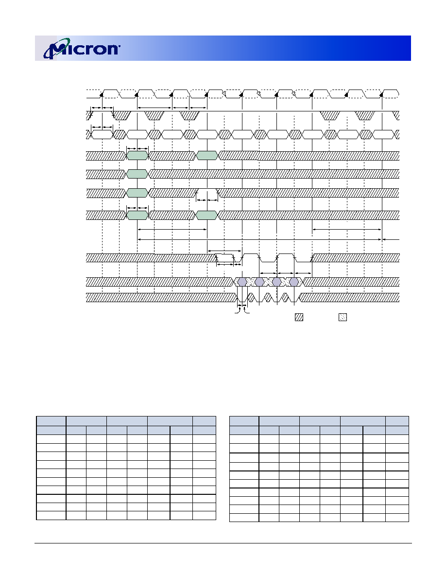
256Mb: x4, x8, x16
DDR SDRAM
09005aef8076894f
Micron Technology, Inc., reserves the right to change products or specifications without notice.
256MBDDRx4x8x16_2.fm - Rev. F 6/03 EN
76
©2003 Micron Technology, Inc.
Figure 51: Bank Write - With Auto Precharge
NOTE:
1. DIn = data-out from column n; subsequent elements are provided in the programmed order.
2. Burst length = 4 in the case shown.
3. Enable auto precharge.
4. ACT = ACTIVE;, RA = Row Address; and BA = Bank Address.
5. NOP commands are shown for ease of illustration; other commands may be valid at these times.
6. See Figure 43, Data Input Timing, on page 68, for detailed DQ timing.
7. Although not required by the Micron device, JEDEC specifies that DQS be a valid HIGH, LOW or some point on a valid
transition on or before this clock edge (T3n).
CK
CK#
CKE
A10
BA0, BA1
t
CK
t
CH
t
CL
t
IS
t
IS
t
IH
t
IS
t
IS
t
IH
t
IH
t
IH
t
IS
t
IH
RA
t
RCD
t
RAS
t
RP
t
WR
T0
T1
T2
T3
T4
T5
T5n
T6
T7
T8
T4n
NOP5
NOP5
COMMAND
4
3
ACT
RA
RA
Col n
WRITE2
NOP5
Bank x
NOP5
Bank x
NOP5
NOP5
NOP5
t
DQSL
t
DQSH
t
WPST
DQ
1
DQS
DM
DI
b
t
DS
t
DH
t
DQSS (NOM)
DON'T CARE
TRANSITIONING DATA
t
WPRES
t
WPRE
x4: A0-A9, A11
x8: A0-A9
x16: A0-A8
x4: A12
x8: A11, A12
x16: A9, A11, A12
T3n
7
-6/6T/6T
-75E/75Z
-75
SYMBOL
MIN
MAX
MIN
MAX
MIN
MAX
UNITS
t
CH
0.45
0.55
0.45
0.55
0.45
0.55
t
CK
t
CL
0.45
0.55
0.45
0.55
0.45
0.55
t
CK
t
CK (2.5)
6
13
7.5
13
7.5
13
ns
t
CK (2)
7.5
13
7.5
13
10
13
ns
t
DH
0.45
0.5
0.5
ns
t
DS
0.45
0.5
0.5
ns
t
DQSH
0.35
0.35
0.35
t
CK
t
DQSL
0.35
0.35
0.35
t
CK
t
DQSS
0.75
1.25
0.75
1.25
0.75
1.25
t
CK
t
DSS
0.2
0.2
0.2
t
CK
t
DSH
0.2
0.2
0.2
t
CK
t
IH
S
0.8
1
1
ns
t
IS
S
0.8
1
1
ns
t
RAS
42
70,000
40
120,000
40
120,000
ns
t
RCD
18
15
20
ns
t
RP
18
15
20
ns
t
WPRE
0.25
0.25
0.25
t
CK
t
WPRES
0
0
0
ns
t
WPST
0.4
0.6
0.4
0.6
0.4
0.6
t
CK
t
WR
15
15
15
ns
-6/6T/6T
-75E/75Z
-75
SYMBOL
MIN
MAX
MIN
MAX
MIN
MAX
UNITS

256Mb: x4, x8, x16
DDR SDRAM
09005aef8076894f
Micron Technology, Inc., reserves the right to change products or specifications without notice.
256MBDDRx4x8x16_2.fm - Rev. F 6/03 EN
77
©2003 Micron Technology, Inc.
Figure 52: Write ≠ DM Operation
NOTE:
1. DIn = data-in from column n; subsequent elements are provided in the programmed order.
2. Burst length = 4 in the case shown.
3. Disable auto precharge.
4. "Don't Care" if A10 is HIGH at T8.
5. PRE = PRECHARGE; ACT = ACTIVE; RA = Row Address; and BA = Bank Address.
6. NOP commands are shown for ease of illustration; other commands may be valid at these times.
7. See Figure 43, Data Input Timing, on page 68, for detailed DQ timing.
8.
Although not required by the Micron device, JEDEC specifies that DQS be a valid HIGH, LOW or some point on a valid
transition on or before this clock edge (T3n).
CK
CK#
CKE
A10
BA0, BA1
t
CK
t
CH
t
CL
t
IS
t
IS
t
IH
t
IS
t
IS
t
IH
t
IH
t
IH
t
IS
t
IH
RA
t
RCD
t
RAS
tRP
tWR
T0
T1
T2
T3
T4
T5
T5n
T6
T7
T8
T4n
NOP6
NOP6
COMMAND
5
3
ACT
RA
RA
Col n
WRITE2
NOP6
ONE BANK
ALL BANKS
Bank x
PRE
Bank x
NOP6
NOP6
NOP6
t
DQSL
t
DQSH
t
WPST
Bank x4
DQ
1
DQS
DM
DI
b
t
DS
t
DH
DON'T CARE
TRANSITIONING DATA
t
DQSS (NOM)
t
WPRES
t
WPRE
x4: A0-A9, A11
x8: A0-A9
x16: A0-A8
x4: A12
x8: A11, A12
x16: A9, A11, A12
8
T3n
-6/6T/6T
-75E/75Z
-75
SYMBOL
MIN
MAX
MIN
MAX
MIN
MAX
UNITS
t
CH
0.45
0.55
0.45
0.55
0.45
0.55
t
CK
t
CL
0.45
0.55
0.45
0.55
0.45
0.55
t
CK
t
CK (2.5)
6
13
7.5
13
7.5
13
ns
t
CK (2)
7.5
13
7.5
13
10
13
ns
t
DH
0.45
0.5
0.5
ns
t
DS
0.45
0.5
0.5
ns
t
DQSH
0.35
0.35
0.35
t
CK
t
DQSL
0.35
0.35
0.35
t
CK
t
DQSS
0.75
1.25
0.75
1.25
0.75
1.25
t
CK
t
DSS
0.2
0.2
0.2
t
CK
t
DSH
0.2
0.2
0.2
t
CK
t
IH
S
0.8
1
1
ns
t
IS
S
0.8
1
1
ns
t
RAS
42
70,000
40
120,000
40
120,000
ns
t
RCD
18
15
20
ns
t
RP
18
15
20
ns
t
WPRE
0.25
0.25
0.25
t
CK
t
WPRES
0
0
0
ns
t
WPST
0.4
0.6
0.4
0.6
0.4
0.6
t
CK
t
WR
15
15
15
ns
-6/6T/6T
-75E/75Z
-75
SYMBOL
MIN
MAX
MIN
MAX
MIN
MAX
UNITS

256Mb: x4, x8, x16
DDR SDRAM
09005aef8076894f
Micron Technology, Inc., reserves the right to change products or specifications without notice.
256MBDDRx4x8x16_2.fm - Rev. F 6/03 EN
78
©2003 Micron Technology, Inc.
Figure 53: 66-Pin Plastic TSOP (400 mil)
NOTE:
1. All dimensionsare in millimeters.
2. Package width and length do not include mold protrusion; allowable mold protrusion is 0.25mm per side.
SEE DETAIL A
0.10
0.65 TYP
0.71
10.16 Ī0.08
0.15
0.50 Ī0.10
PIN #1 ID
DETAIL A
22.22 Ī 0.08
0.32 Ī0.075 TYP
+0.03
-0.02
+0.10
-0.05
1.20 MAX
0.10
0.25
11.76 Ī0.10
0.80 TYP
0.10 (2X)
GAGE PLANE

256Mb: x4, x8, x16
DDR SDRAM
09005aef8076894f
Micron Technology, Inc., reserves the right to change products or specifications without notice.
256MBDDRx4x8x16_2.fm - Rev. F 6/03 EN
79
©2003 Micron Technology, Inc.
Figure 54: 60-Ball FBGA (16 x 9mm)
NOTE:
All dimensions are in millimeters.
BALL #1 ID
SOLDER BALL MATERIAL: EUTECTIC 63% Sn, 37% Pb or
62% Sn, 36% Pb, 2% Ag
SOLDER BALL PAD: ō .33mm
MOLD COMPOUND: EPOXY NOVOLAC
SUBSTRATE: PLASTIC LAMINATE
BALL A1
BALL A1 ID
C
L
C
L
0.850 Ī0.075
0.10 C
C
.45
60X ō
SOLDER BALL DIAMETER REFERS TO
POST REFLOW CONDITION. THE
PRE-REFLOW DIAMETER IS ō 0.40mm.
BALL A9
11.00
5.50 Ī0.05
8.00 Ī0.05
16.00 Ī0.10
1.00
TYP
0.80
TYP
6.40
3.20 Ī0.05 4.50 Ī0.05
9.00 Ī0.10
1.20 MAX
SEATING PLANE
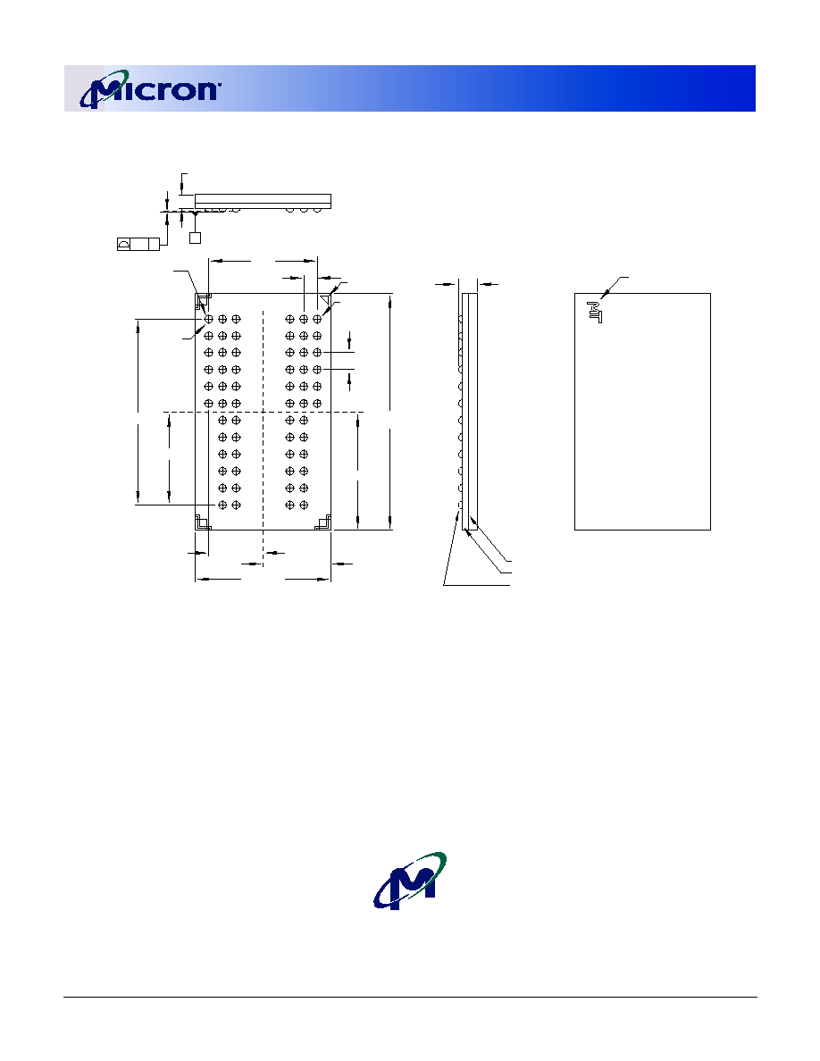
256Mb: x4, x8, x16
DDR SDRAM
09005aef8076894f
Micron Technology, Inc., reserves the right to change products or specifications without notice..
256MBDDRx4x8x16_2.fm - Rev. F 6/03 EN
80
©2003 Micron Technology, Inc
ģ
8000 S. Federal Way, P.O. Box 6, Boise, ID 83707-0006, Tel: 208-368-3900
E-mail: prodmktg@micron.com, Internet: http://www.micron.com, Customer Comment Line: 800-932-4992
Micron, the M logo, and the Micron logo are trademarks and/or service marks of Micron Technology, Inc.
All other trademarks are the property of their respective owners.
Figure 55: 60-Ball FBGA (14 x 8mm)
NOTE:
All dimensions are in millimeters.
Data Sheet Designation
This data sheet contains minimum and maximum
limits specified over the complete power supply and
temperature range for production devices. Although
considered final, these specifications are subject to
change, as further product development and data
characterization sometimes occur.
PIN A1 ID
1.20 MAX
MOLD COMPOUND: EPOXY NOVOLAC
SUBSTRATE: PLASTIC LAMINATE
SOLDER BALL MATERIAL: EUTECTIC 62% Sn, 36% Pb, 2%Ag
SOLDER BALL PAD: ō .33mm
14.00 Ī0.10
BALL A1
BALL A9
PIN A1 ID
1.00 TYP
0.80 TYP
7.00 Ī0.05
8.00 Ī0.10
4.00 Ī0.05
3.20 Ī0.05
5.50 Ī0.05
0.850 Ī0.075
SEATING PLANE
C
11.00
6.40
0.10 C
60X
0.45
SOLDER BALL DIAMETER
REFERS TO POST REFLOW
CONDITION. THE PRE-
REFLOW DIAMETER IS ō 0.40
C
L
C
L