
PRELIMINARY DATA SHEET
SDA 6000, SDA 6001
Version B11
Teletext Decoder
with Embedded
16-bit Controller
M2
Edition Feb. 8, 2002
6251-557-2PD

Contents
Pin Description
Architectural Overview
C16X Microcontroller
Interrupt and Trap Function
Peripherals
Clock System
Display Generator
D/A Converter
Slicer and Acquisition
Electrical Characteristics
System Control & Configuration
Register Overview
Sync System
Overview

For questions on technology, delivery and prices please contact the Micronas Offices in Germany
or the Micronas GmbH Companies and Representatives worldwide:
see our webpage at http://www.micronas.com
SDA 6000
Revision History:
Current Version: 2002-01-08
Previous Version:
03.01
Page
Subjects (major changes since last revision)
Update to all B11 design step related features:
- Double Resolution for interlaced video signals (only SDA6001)
- Testmode activation for switching bidirectional pins to input
- Modifications to Slicer module
- Digital RGB interface
- Refresh Cycle Control of SDRAM
- I�C bus levels
Furthermore corrections of spelling, inconsistences, ...

SDA 6000 / SDA 6001
PRELIMINARY DATA SHEET
Version 3.00
- 1
Micronas
1
Overview . . . . . . . . . . . . . . . . . . . . . . . . . . . . . . . . . . . . . . . . . . . . . . . . 1 - 3
1.1
Features . . . . . . . . . . . . . . . . . . . . . . . . . . . . . . . . . . . . . . . . . . . . . . . . . 1 - 7
1.2
Logic Symbol . . . . . . . . . . . . . . . . . . . . . . . . . . . . . . . . . . . . . . . . . . . . . 1 - 9
2
Pin Descriptions . . . . . . . . . . . . . . . . . . . . . . . . . . . . . . . . . . . . . . . . . 2 - 3
2.1
Pin Diagram (top view) . . . . . . . . . . . . . . . . . . . . . . . . . . . . . . . . . . . . . 2 - 4
2.2
Pin Definitions and Functions . . . . . . . . . . . . . . . . . . . . . . . . . . . . . . . . 2 - 5
3
Architectural Overview . . . . . . . . . . . . . . . . . . . . . . . . . . . . . . . . . . . . 3 - 3
4
C16X Microcontroller . . . . . . . . . . . . . . . . . . . . . . . . . . . . . . . . . . . . . . 4 - 3
4.1
Overview . . . . . . . . . . . . . . . . . . . . . . . . . . . . . . . . . . . . . . . . . . . . . . . . 4 - 4
4.2
Memory Organization . . . . . . . . . . . . . . . . . . . . . . . . . . . . . . . . . . . . . . 4 - 7
4.3
On-Chip Microcontroller RAM and SFR Area . . . . . . . . . . . . . . . . . . . 4 - 10
4.3.1
System Stack . . . . . . . . . . . . . . . . . . . . . . . . . . . . . . . . . . . . . . . . . 4 - 11
4.3.2
General Purpose Registers . . . . . . . . . . . . . . . . . . . . . . . . . . . . . . . 4 - 12
4.3.3
PEC Source and Destination Pointers . . . . . . . . . . . . . . . . . . . . . . . 4 - 13
4.3.4
Special Function Registers . . . . . . . . . . . . . . . . . . . . . . . . . . . . . . . 4 - 14
4.4
External Memory . . . . . . . . . . . . . . . . . . . . . . . . . . . . . . . . . . . . . . . . . 4 - 16
4.4.1
SDRAM . . . . . . . . . . . . . . . . . . . . . . . . . . . . . . . . . . . . . . . . . . . . . . 4 - 16
4.4.2
External Static Memory Devices . . . . . . . . . . . . . . . . . . . . . . . . . . . 4 - 16
4.5
External Bus Interface (EBI). . . . . . . . . . . . . . . . . . . . . . . . . . . . . . . . . 4 - 18
4.5.1
Memory Mapping . . . . . . . . . . . . . . . . . . . . . . . . . . . . . . . . . . . . . . . 4 - 20
4.5.2
Register Description . . . . . . . . . . . . . . . . . . . . . . . . . . . . . . . . . . . . 4 - 23
4.5.3
Crossing Memory Boundaries . . . . . . . . . . . . . . . . . . . . . . . . . . . . 4 - 29
4.6
Central Processing Unit . . . . . . . . . . . . . . . . . . . . . . . . . . . . . . . . . . . . 4 - 31
4.6.1
Instruction Pipelining . . . . . . . . . . . . . . . . . . . . . . . . . . . . . . . . . . . . 4 - 32
4.6.2
Bit-Handling and Bit-Protection . . . . . . . . . . . . . . . . . . . . . . . . . . . 4 - 38
4.6.3
Instruction State Times . . . . . . . . . . . . . . . . . . . . . . . . . . . . . . . . . 4 - 39
4.6.4
CPU Special Function Registers . . . . . . . . . . . . . . . . . . . . . . . . . . . 4 - 40
5
Interrupt and Trap Functions . . . . . . . . . . . . . . . . . . . . . . . . . . . . . . . 5 - 3
5.1
Interrupt System Structure . . . . . . . . . . . . . . . . . . . . . . . . . . . . . . . . . . . 5 - 4
5.1.1
Interrupt Allocation Table . . . . . . . . . . . . . . . . . . . . . . . . . . . . . . . . . . 5 - 4
5.1.2
Hardware Traps . . . . . . . . . . . . . . . . . . . . . . . . . . . . . . . . . . . . . . . . . 5 - 6
5.2
Operation of the PEC Channels . . . . . . . . . . . . . . . . . . . . . . . . . . . . 5 - 14
5.2.1
Prioritization of Interrupt and PEC Service Requests . . . . . . . . . . . 5 - 20
5.2.2
Saving the Status during Interrupt Service . . . . . . . . . . . . . . . . . . . 5 - 22
5.2.3
Interrupt Response Times . . . . . . . . . . . . . . . . . . . . . . . . . . . . . . . 5 - 23
5.2.4
PEC Response Times . . . . . . . . . . . . . . . . . . . . . . . . . . . . . . . . . . 5 - 25
5.2.5
Fast Interrupts . . . . . . . . . . . . . . . . . . . . . . . . . . . . . . . . . . . . . . . . 5 - 27
5.3
Trap Functions . . . . . . . . . . . . . . . . . . . . . . . . . . . . . . . . . . . . . . . . . . 5 - 29
5.3.1
External Interrupt Source Control . . . . . . . . . . . . . . . . . . . . . . . . . . 5 - 34
6
System Control & Configuration . . . . . . . . . . . . . . . . . . . . . . . . . . . . 6 - 3

SDA 6000 / SDA 6001
PRELIMINARY DATA SHEET
Version 3.00
- 2
Micronas
6.1
System Reset . . . . . . . . . . . . . . . . . . . . . . . . . . . . . . . . . . . . . . . . . . . . 6 - 4
6.1.1
Behavior of I/Os during Reset . . . . . . . . . . . . . . . . . . . . . . . . . . . . . . 6 - 5
6.1.2
Reset Values for the Controller Core Registers . . . . . . . . . . . . . . . . . 6 - 5
6.1.3
The Internal RAM after Reset . . . . . . . . . . . . . . . . . . . . . . . . . . . . . . 6 - 6
6.2
System Start-up Configuration . . . . . . . . . . . . . . . . . . . . . . . . . . . . . . . . 6 - 7
6.3
Register Write Protection . . . . . . . . . . . . . . . . . . . . . . . . . . . . . . . . . . . . 6 - 9
6.4
Power Reduction Modes . . . . . . . . . . . . . . . . . . . . . . . . . . . . . . . . . . . 6 - 13
6.5
Dedicated Pins . . . . . . . . . . . . . . . . . . . . . . . . . . . . . . . . . . . . . . . . . . . 6 - 17
6.6
XBUS Configuration . . . . . . . . . . . . . . . . . . . . . . . . . . . . . . . . . . . . . . . 6 - 19
6.7
Watchdog Timer . . . . . . . . . . . . . . . . . . . . . . . . . . . . . . . . . . . . . . . . . 6 - 20
6.8
Bootstrap Loader . . . . . . . . . . . . . . . . . . . . . . . . . . . . . . . . . . . . . . . . . 6 - 24
6.9
Identification Registers . . . . . . . . . . . . . . . . . . . . . . . . . . . . . . . . . . . . 6 - 26
6.9.1
System Identification . . . . . . . . . . . . . . . . . . . . . . . . . . . . . . . . . . . . 6 - 26
6.9.2
CPU Identification . . . . . . . . . . . . . . . . . . . . . . . . . . . . . . . . . . . . . . 6 - 29
6.10
Parallel Ports . . . . . . . . . . . . . . . . . . . . . . . . . . . . . . . . . . . . . . . . . . . . 6 - 30
6.11
On board FLASH/EPROM-programming . . . . . . . . . . . . . . . . . . . . . . . 6 - 39
7
Peripherals . . . . . . . . . . . . . . . . . . . . . . . . . . . . . . . . . . . . . . . . . . . . . . 7 - 3
7.1
General Purpose Timer Unit . . . . . . . . . . . . . . . . . . . . . . . . . . . . . . . . . 7 - 4
7.1.1
Functional Description of Timer Block 1 . . . . . . . . . . . . . . . . . . . . . . 7 - 4
7.1.1.1
Timer Concatenation . . . . . . . . . . . . . . . . . . . . . . . . . . . . . . . . . . 7 - 15
7.1.2
Functional Description of Timer Block 2 . . . . . . . . . . . . . . . . . . . . . 7 - 20
7.1.2.1
Core Timer T6 . . . . . . . . . . . . . . . . . . . . . . . . . . . . . . . . . . . . . . . 7 - 21
7.1.2.2
Auxiliary Timer T5 . . . . . . . . . . . . . . . . . . . . . . . . . . . . . . . . . . . . 7 - 22
7.1.2.3
Timer Concatenation . . . . . . . . . . . . . . . . . . . . . . . . . . . . . . . . . . 7 - 23
7.1.3
GPT Registers . . . . . . . . . . . . . . . . . . . . . . . . . . . . . . . . . . . . . . . . . 7 - 27
7.1.4
Interrupts . . . . . . . . . . . . . . . . . . . . . . . . . . . . . . . . . . . . . . . . . . . . . 7 - 38
7.2
Real-time Clock . . . . . . . . . . . . . . . . . . . . . . . . . . . . . . . . . . . . . . . . . . 7 - 40
7.2.1
General Description . . . . . . . . . . . . . . . . . . . . . . . . . . . . . . . . . . . . . 7 - 40
7.2.2
Register Description . . . . . . . . . . . . . . . . . . . . . . . . . . . . . . . . . . . . 7 - 42
7.3
Asynchronous/Synchronous Serial Interface . . . . . . . . . . . . . . . . . . . . 7 - 47
7.3.1
Asynchronous Operation . . . . . . . . . . . . . . . . . . . . . . . . . . . . . . . . . 7 - 50
7.3.1.1
Asynchronous Data Frames . . . . . . . . . . . . . . . . . . . . . . . . . . . . 7 - 52
7.3.1.2
Asynchronous Transmission . . . . . . . . . . . . . . . . . . . . . . . . . . . . 7 - 54
7.3.1.3
Asynchronous Reception . . . . . . . . . . . . . . . . . . . . . . . . . . . . . . . 7 - 55
7.3.2
Synchronous Operation . . . . . . . . . . . . . . . . . . . . . . . . . . . . . . . . . . 7 - 57
7.3.2.1
Synchronous Transmission . . . . . . . . . . . . . . . . . . . . . . . . . . . . . 7 - 58
7.3.2.2
Synchronous Reception . . . . . . . . . . . . . . . . . . . . . . . . . . . . . . . . 7 - 59
7.3.2.3
Synchronous Timing . . . . . . . . . . . . . . . . . . . . . . . . . . . . . . . . . . 7 - 59
7.3.3
Baud Rate Generation . . . . . . . . . . . . . . . . . . . . . . . . . . . . . . . . . . . 7 - 60
7.3.3.1
Baud Rates in Asynchronous Mode . . . . . . . . . . . . . . . . . . . . . . 7 - 61
7.3.3.2
Baud Rates in Synchronous Mode . . . . . . . . . . . . . . . . . . . . . . . 7 - 64
7.3.4
Autobaud Detection . . . . . . . . . . . . . . . . . . . . . . . . . . . . . . . . . . . . . 7 - 64

SDA 6000 / SDA 6001
PRELIMINARY DATA SHEET
Version 3.00
- 3
Micronas
7.3.4.1
Serial Frames for Autobaud Detection . . . . . . . . . . . . . . . . . . . . . 7 - 65
7.3.4.2
Baud Rate Selection and Calculation . . . . . . . . . . . . . . . . . . . . . 7 - 68
7.3.4.3
Overwriting Registers on Successful Autobaud Detection . . . . . 7 - 70
7.3.5
ASC Hardware Error Detection Capabilities . . . . . . . . . . . . . . . . . . 7 - 71
7.3.6
Interrupts . . . . . . . . . . . . . . . . . . . . . . . . . . . . . . . . . . . . . . . . . . . . . 7 - 72
7.3.7
Register Description . . . . . . . . . . . . . . . . . . . . . . . . . . . . . . . . . . . . 7 - 73
7.4
High Speed Synchronous Serial Interface . . . . . . . . . . . . . . . . . . . . . . 7 - 83
7.4.1
Full-Duplex Operation . . . . . . . . . . . . . . . . . . . . . . . . . . . . . . . . . . . 7 - 87
7.4.2
Half Duplex Operation . . . . . . . . . . . . . . . . . . . . . . . . . . . . . . . . . . . 7 - 90
7.4.3
Continuous Transfers . . . . . . . . . . . . . . . . . . . . . . . . . . . . . . . . . . . 7 - 91
7.4.4
Port Control . . . . . . . . . . . . . . . . . . . . . . . . . . . . . . . . . . . . . . . . . . . 7 - 92
7.4.5
Baud Rate Generation . . . . . . . . . . . . . . . . . . . . . . . . . . . . . . . . . . . 7 - 92
7.4.6
Error Detection Mechanisms . . . . . . . . . . . . . . . . . . . . . . . . . . . . . . 7 - 93
7.4.7
Register Description . . . . . . . . . . . . . . . . . . . . . . . . . . . . . . . . . . . . 7 - 96
7.5
I2C-Bus Interface . . . . . . . . . . . . . . . . . . . . . . . . . . . . . . . . . . . . . . . . 7 - 101
7.5.1
Operational Overview . . . . . . . . . . . . . . . . . . . . . . . . . . . . . . . . . . 7 - 101
7.5.2
The Physical I
2
C-Bus Interface . . . . . . . . . . . . . . . . . . . . . . . . . . . 7 - 102
7.5.3
Functional Overview . . . . . . . . . . . . . . . . . . . . . . . . . . . . . . . . . . . 7 - 105
7.5.4
Registers . . . . . . . . . . . . . . . . . . . . . . . . . . . . . . . . . . . . . . . . . . . . 7 - 107
7.6
Analog Digital Converter . . . . . . . . . . . . . . . . . . . . . . . . . . . . . . . . . . 7 - 121
7.6.1
Power Down and Wake Up . . . . . . . . . . . . . . . . . . . . . . . . . . . . . . 7 - 121
7.6.2
Register Description . . . . . . . . . . . . . . . . . . . . . . . . . . . . . . . . . . . 7 - 122
8
Clock System . . . . . . . . . . . . . . . . . . . . . . . . . . . . . . . . . . . . . . . . . . . . 8 - 3
8.1
General Function . . . . . . . . . . . . . . . . . . . . . . . . . . . . . . . . . . . . . . . . . . 8 - 4
8.2
Register Description . . . . . . . . . . . . . . . . . . . . . . . . . . . . . . . . . . . . . . . 8 - 6
9
Sync System . . . . . . . . . . . . . . . . . . . . . . . . . . . . . . . . . . . . . . . . . . . . 9 - 3
9.1
General Description . . . . . . . . . . . . . . . . . . . . . . . . . . . . . . . . . . . . . . . . 9 - 4
9.1.1
Screen Resolution . . . . . . . . . . . . . . . . . . . . . . . . . . . . . . . . . . . . . . . 9 - 4
9.1.2
Sync Interrupts . . . . . . . . . . . . . . . . . . . . . . . . . . . . . . . . . . . . . . . . . . 9 - 6
9.2
Register Description . . . . . . . . . . . . . . . . . . . . . . . . . . . . . . . . . . . . . . . 9 - 7
9.3
Double Resolution combined with interlaced video signals Ionly SDA6001) 9
- 17
9.3.1
Sync rasters . . . . . . . . . . . . . . . . . . . . . . . . . . . . . . . . . . . . . . . . . . . 9 - 17
9.3.1.1
50Hz/100Hz Mode (ABAB) . . . . . . . . . . . . . . . . . . . . . . . . . . . . . 9 - 18
9.3.1.2
100 Hz Mode (AABB) . . . . . . . . . . . . . . . . . . . . . . . . . . . . . . . . . 9 - 19
9.3.1.3
100 Hz Mode (AAAA) . . . . . . . . . . . . . . . . . . . . . . . . . . . . . . . . . 9 - 20
9.3.2
Registers important for double resolution . . . . . . . . . . . . . . . . . . . . 9 - 20
9.3.3
Implementation details . . . . . . . . . . . . . . . . . . . . . . . . . . . . . . . . . . . 9 - 21
9.3.3.1
Field detection . . . . . . . . . . . . . . . . . . . . . . . . . . . . . . . . . . . . . . . 9 - 21
9.3.3.2
Splitting of the frames(Layer1/Layer2) within frame buffer to display ras-
ter 9 - 23

SDA 6000 / SDA 6001
PRELIMINARY DATA SHEET
Version 3.00
- 4
Micronas
10
Display Generator . . . . . . . . . . . . . . . . . . . . . . . . . . . . . . . . . . . . . . . 10 - 3
10.1
General Description . . . . . . . . . . . . . . . . . . . . . . . . . . . . . . . . . . . . . . . 10 - 4
10.2
Screen Alignments . . . . . . . . . . . . . . . . . . . . . . . . . . . . . . . . . . . . . . . . 10 - 5
10.3
Layer Concept . . . . . . . . . . . . . . . . . . . . . . . . . . . . . . . . . . . . . . . . . . . 10 - 7
10.3.1
Overlapped Layers . . . . . . . . . . . . . . . . . . . . . . . . . . . . . . . . . . . . . 10 - 8
10.3.2
Embedded Layers . . . . . . . . . . . . . . . . . . . . . . . . . . . . . . . . . . . . . 10 - 10
10.3.3
Transparency in Screen Background Area . . . . . . . . . . . . . . . . . . 10 - 11
10.4
Input and Output Formats . . . . . . . . . . . . . . . . . . . . . . . . . . . . . . . . . 10 - 14
10.4.1
Input Formats . . . . . . . . . . . . . . . . . . . . . . . . . . . . . . . . . . . . . . . . . 10 - 15
10.4.2
Output Formats . . . . . . . . . . . . . . . . . . . . . . . . . . . . . . . . . . . . . . . 10 - 16
10.5
Initialization of Memory Transfers . . . . . . . . . . . . . . . . . . . . . . . . . . . 10 - 20
10.5.1
Transfer Modes . . . . . . . . . . . . . . . . . . . . . . . . . . . . . . . . . . . . . . . 10 - 20
10.5.2
Transfer Areas . . . . . . . . . . . . . . . . . . . . . . . . . . . . . . . . . . . . . . . . 10 - 23
10.5.3
Italic Mode . . . . . . . . . . . . . . . . . . . . . . . . . . . . . . . . . . . . . . . . . . . 10 - 28
10.6
Register Description . . . . . . . . . . . . . . . . . . . . . . . . . . . . . . . . . . . . . 10 - 30
10.6.1
Special Function Registers . . . . . . . . . . . . . . . . . . . . . . . . . . . . . . 10 - 30
10.7
Description of Graphic Accelerator Instructions . . . . . . . . . . . . . . . . . 10 - 33
10.7.1
Screen Attributes (SAR) . . . . . . . . . . . . . . . . . . . . . . . . . . . . . . . . 10 - 35
10.7.2
Startaddress of Layer 1 (FBR) . . . . . . . . . . . . . . . . . . . . . . . . . . . . 10 - 38
10.7.3
Size of Layer 1 (FSR) . . . . . . . . . . . . . . . . . . . . . . . . . . . . . . . . . . 10 - 38
10.7.4
Startaddress of Layer 2 (DBR) . . . . . . . . . . . . . . . . . . . . . . . . . . . 10 - 39
10.7.5
Size of Layer 2 (DSR) . . . . . . . . . . . . . . . . . . . . . . . . . . . . . . . . . . 10 - 39
10.7.6
Display Coordinates of Layer 2 (DCR) . . . . . . . . . . . . . . . . . . . . . 10 - 40
10.7.7
Contents of CLUT (CLR) . . . . . . . . . . . . . . . . . . . . . . . . . . . . . . . . 10 - 41
10.7.8
Clipping Coordinates (CUR and CBR) . . . . . . . . . . . . . . . . . . . . . . 10 - 41
10.7.9
Source Descriptor for Data Transfer (SDR) . . . . . . . . . . . . . . . . . . 10 - 43
10.7.10
Source Size of Transferred Memory Area (TSR) . . . . . . . . . . . . . . 10 - 44
10.7.11
Destination Size of Transferred Memory Area (TDR) . . . . . . . . . . 10 - 45
10.7.12
Offset of Transferred Memory Area (TOR) . . . . . . . . . . . . . . . . . . 10 - 46
10.7.13
Attributes of Transfer (TAR) . . . . . . . . . . . . . . . . . . . . . . . . . . . . . . 10 - 47
10.8
Digital RGB interface . . . . . . . . . . . . . . . . . . . . . . . . . . . . . . . . . . . . . 10 - 49
10.8.1
General . . . . . . . . . . . . . . . . . . . . . . . . . . . . . . . . . . . . . . . . . . . . . 10 - 49
10.8.2
Ports used for digital RGB Interface . . . . . . . . . . . . . . . . . . . . . . . 10 - 50
10.8.3
Registers used for the digital RGB interface . . . . . . . . . . . . . . . . . 10 - 51
11
D/A Converter . . . . . . . . . . . . . . . . . . . . . . . . . . . . . . . . . . . . . . . . . . . 11 - 3
11.1
Register Description . . . . . . . . . . . . . . . . . . . . . . . . . . . . . . . . . . . . . . 11 - 4
12
Slicer and Acquisition . . . . . . . . . . . . . . . . . . . . . . . . . . . . . . . . . . . . 12 - 3
12.1
General Function . . . . . . . . . . . . . . . . . . . . . . . . . . . . . . . . . . . . . . . . . 12 - 4
12.2
Slicer Architecture . . . . . . . . . . . . . . . . . . . . . . . . . . . . . . . . . . . . . . . . 12 - 5
12.2.1
Distortion Processing . . . . . . . . . . . . . . . . . . . . . . . . . . . . . . . . . . . . 12 - 7
12.3
H/V-Synchronization . . . . . . . . . . . . . . . . . . . . . . . . . . . . . . . . . . . . . . 12 - 8
12.4
Acquisition Interface . . . . . . . . . . . . . . . . . . . . . . . . . . . . . . . . . . . . . . 12 - 9

SDA 6000 / SDA 6001
PRELIMINARY DATA SHEET
Version 3.00
- 5
Micronas
12.4.1
FC-Check . . . . . . . . . . . . . . . . . . . . . . . . . . . . . . . . . . . . . . . . . . . . . 12 - 9
12.4.2
Interrupts . . . . . . . . . . . . . . . . . . . . . . . . . . . . . . . . . . . . . . . . . . . . 12 - 10
12.4.3
VBI Buffer and Memory Organization . . . . . . . . . . . . . . . . . . . . . . 12 - 10
12.5
Register Description . . . . . . . . . . . . . . . . . . . . . . . . . . . . . . . . . . . . . 12 - 13
12.5.1
RAM Registers . . . . . . . . . . . . . . . . . . . . . . . . . . . . . . . . . . . . . . . . 12 - 16
12.5.2
Recommended Parameter Settings . . . . . . . . . . . . . . . . . . . . . . . . 12 - 31
13
Register Overview . . . . . . . . . . . . . . . . . . . . . . . . . . . . . . . . . . . . . . 13 - 3
13.1
Register Description Format . . . . . . . . . . . . . . . . . . . . . . . . . . . . . . . . 13 - 4
13.2
CPU General Purpose Registers (GPRs) . . . . . . . . . . . . . . . . . . . . . 13 - 5
13.3
Registers Ordered by Context . . . . . . . . . . . . . . . . . . . . . . . . . . . . . . 13 - 7
13.4
Registers Ordered by Address . . . . . . . . . . . . . . . . . . . . . . . . . . . . . 13 - 17
13.4.1
Registers in SFR Area . . . . . . . . . . . . . . . . . . . . . . . . . . . . . . . . . . 13 - 18
13.4.2
Registers in ESFR Area . . . . . . . . . . . . . . . . . . . . . . . . . . . . . . . . . 13 - 19
14
Electrical Characteristics . . . . . . . . . . . . . . . . . . . . . . . . . . . . . . . . . 14 - 3
14.1
Absolute Maximum Ratings . . . . . . . . . . . . . . . . . . . . . . . . . . . . . . . . . 14 - 4
14.2
Operating Range . . . . . . . . . . . . . . . . . . . . . . . . . . . . . . . . . . . . . . . . . 14 - 5
14.3
DC Characteristics . . . . . . . . . . . . . . . . . . . . . . . . . . . . . . . . . . . . . . . . 14 - 6
14.4
Timings . . . . . . . . . . . . . . . . . . . . . . . . . . . . . . . . . . . . . . . . . . . . . . . 14 - 14
14.5
Package Outlines . . . . . . . . . . . . . . . . . . . . . . . . . . . . . . . . . . . . . . . . 14 - 15

SDA 6000 / SDA 6001
PRELIMINARY DATA SHEET
Version 3.00
- 1
Micronas
Figure 1-1
M2 Tool Flow . . . . . . . . . . . . . . . . . . . . . . . . . . . . . . . . . . . . . . . . . . 1 - 5
Figure 1-2
Logic Symbol . . . . . . . . . . . . . . . . . . . . . . . . . . . . . . . . . . . . . . . . . . 1 - 9
Figure 2-1
Pin Configuration . . . . . . . . . . . . . . . . . . . . . . . . . . . . . . . . . . . . . . . 2 - 4
Figure 3-1
M2 Top Level Block Diagram. . . . . . . . . . . . . . . . . . . . . . . . . . . . . . 3 - 3
Figure 4-1
M2 Memory Path Block Diagram . . . . . . . . . . . . . . . . . . . . . . . . . . . 4 - 8
Figure 4-2
Storage of Words, Byte and Bits in a Byte Organized Memory . . . . 4 - 9
Figure 4-3
Internal RAM Areas and SFR Areas . . . . . . . . . . . . . . . . . . . . . . . 4 - 10
Figure 4-4
Location of the PEC Pointers. . . . . . . . . . . . . . . . . . . . . . . . . . . . . 4 - 13
Figure 4-5
External Memory Configuration . . . . . . . . . . . . . . . . . . . . . . . . . . . 4 - 18
Figure 4-6
Interlocked Access Cycles to ROM and SDRAM. . . . . . . . . . . . . . 4 - 19
Figure 4-7
Interlocked Access Cycles to two SDRAM Banks . . . . . . . . . . . . . 4 - 20
Figure 4-8
Memory Mapping . . . . . . . . . . . . . . . . . . . . . . . . . . . . . . . . . . . . . . 4 - 21
Figure 4-9
Four-Phase Handshake . . . . . . . . . . . . . . . . . . . . . . . . . . . . . . . . . 4 - 26
Figure 4-10
CPU Block Diagram . . . . . . . . . . . . . . . . . . . . . . . . . . . . . . . . . . . . 4 - 31
Figure 4-11
Sequential Instruction Pipelining . . . . . . . . . . . . . . . . . . . . . . . . . . 4 - 34
Figure 4-12
Standard Branch Instruction Pipelining . . . . . . . . . . . . . . . . . . . . . 4 - 34
Figure 4-13
Cache Jump Instruction Pipelining. . . . . . . . . . . . . . . . . . . . . . . . . 4 - 35
Figure 4-14
Addressing via the Code Segment Pointer . . . . . . . . . . . . . . . . . . 4 - 48
Figure 4-15
Addressing via the Data Page Pointers . . . . . . . . . . . . . . . . . . . . . 4 - 50
Figure 4-16
Register Bank Selection via Register CP. . . . . . . . . . . . . . . . . . . . 4 - 51
Figure 4-17
Implicit CP Use by Short GPR Addressing Modes . . . . . . . . . . . . 4 - 52
Figure 5-1
Priority Levels and PEC Channels. . . . . . . . . . . . . . . . . . . . . . . . . 5 - 10
Figure 5-2
Mapping of PEC Offset Pointers into the Internal RAM . . . . . . . . . 5 - 19
Figure 5-3
Task Status Saved on the System Stack. . . . . . . . . . . . . . . . . . . . 5 - 22
Figure 5-4
Pipeline Diagram for Interrupt Response Time . . . . . . . . . . . . . . . 5 - 23
Figure 5-5
Pipeline Diagram for PEC Response Time . . . . . . . . . . . . . . . . . . 5 - 26
Figure 6-1
State Machine for Security Level Switching. . . . . . . . . . . . . . . . . . 6 - 12
Figure 6-2
Transitions between Idle Mode and Active Mode . . . . . . . . . . . . . 6 - 15
Figure 6-3
WDT Block Diagram . . . . . . . . . . . . . . . . . . . . . . . . . . . . . . . . . . . 6 - 20
Figure 6-4
Bootstrap Loader Sequence . . . . . . . . . . . . . . . . . . . . . . . . . . . . . 6 - 24
Figure 6-5
Portlogic Register Overview. . . . . . . . . . . . . . . . . . . . . . . . . . . . . . 6 - 30
Figure 6-6
Entering of testmode to switch all bidirectional ports to input . . . . 6 - 39
Figure 6-7
Leaving of testmode. . . . . . . . . . . . . . . . . . . . . . . . . . . . . . . . . . . . 6 - 40
Figure 7-1
Structure of Timer Block 1 Core Timer T3 . . . . . . . . . . . . . . . . . . . . 7 - 5
Figure 7-2
Block Diagram of Core Timer T3 in Timer Mode . . . . . . . . . . . . . . . 7 - 8
Figure 7-3
Block Diagram of Core Timer T3 in Gated Timer Mode. . . . . . . . . . 7 - 8
Figure 7-4
Block Diagram of Core Timer T3 in Counter Mode . . . . . . . . . . . . . 7 - 9
Figure 7-5
Block Diagram of Core Timer T3 in Incremental Interface Mode. . 7 - 10
Figure 7-6
Interfacing the Encoder to the Microcontroller . . . . . . . . . . . . . . . . 7 - 11
Figure 7-7
Evaluation of the Incremental Encoder Signals . . . . . . . . . . . . . . . 7 - 12
Figure 7-8
Evaluation of the Incremental Encoder Signals . . . . . . . . . . . . . . . 7 - 13
Figure 7-9
Block Diagram of an Auxiliary Timer in Counter Mode . . . . . . . . . 7 - 14
Figure 7-10
Concatenation of Core Timer T3 and an Auxiliary Timer. . . . . . . . 7 - 16

SDA 6000 / SDA 6001
PRELIMINARY DATA SHEET
Version 3.00
- 2
Micronas
Figure 7-11
GPT1 Auxiliary Timer in Reload Mode. . . . . . . . . . . . . . . . . . . . . . 7 - 17
Figure 7-12
GPT1 Timer Reload Configuration for PWM Generation. . . . . . . . 7 - 18
Figure 7-13
Auxiliary Timer of Timer Block 1 in Capture Mode. . . . . . . . . . . . . 7 - 19
Figure 7-14
Structure of Timer Block 2 . . . . . . . . . . . . . . . . . . . . . . . . . . . . . . . 7 - 20
Figure 7-15
Block Diagram of Core Timer T6 in Timer Mode . . . . . . . . . . . . . . 7 - 22
Figure 7-16
Concatenation of Core Timer T6 and Auxiliary Timer T5. . . . . . . . 7 - 23
Figure 7-17
Timer Block 2 Register CAPREL in Capture Mode . . . . . . . . . . . . 7 - 24
Figure 7-18
Timer Block 2 Register CAPREL in Reload Mode . . . . . . . . . . . . . 7 - 25
Figure 7-19
Timer Block 2 Register CAPREL in Capture-And-Reload Mode . . 7 - 26
Figure 7-20
RTC Register Overview . . . . . . . . . . . . . . . . . . . . . . . . . . . . . . . . . 7 - 40
Figure 7-21
RTC Block Diagram . . . . . . . . . . . . . . . . . . . . . . . . . . . . . . . . . . . . 7 - 41
Figure 7-22
Block Diagram of the ASC0 . . . . . . . . . . . . . . . . . . . . . . . . . . . . . . 7 - 48
Figure 7-23
ASC Register Overview . . . . . . . . . . . . . . . . . . . . . . . . . . . . . . . . . 7 - 49
Figure 7-24
Asynchronous Mode of Serial Channel ASC0 . . . . . . . . . . . . . . . . 7 - 51
Figure 7-25
Asynchronous 8-Bit Frames. . . . . . . . . . . . . . . . . . . . . . . . . . . . . . 7 - 52
Figure 7-26
Asynchronous 9-Bit Frames. . . . . . . . . . . . . . . . . . . . . . . . . . . . . . 7 - 53
Figure 7-27
IrDA Frame Encoding/Decoding . . . . . . . . . . . . . . . . . . . . . . . . . . 7 - 54
Figure 7-28
Fixed IrDA Pulse Generation . . . . . . . . . . . . . . . . . . . . . . . . . . . . . 7 - 56
Figure 7-29
RXD/TXD Data Path in Asynchronous Modes. . . . . . . . . . . . . . . . 7 - 57
Figure 7-30
Synchronous Mode of Serial Channel ASC0 . . . . . . . . . . . . . . . . . 7 - 58
Figure 7-31
ASC0 Synchronous Mode Waveforms . . . . . . . . . . . . . . . . . . . . . 7 - 60
Figure 7-32
ASC0 Baud Rate Generator Circuitry in Asynchronous Modes. . . 7 - 62
Figure 7-33
ASC0 Baud Rate Generator Circuitry in Synchronous Mode . . . . 7 - 64
Figure 7-34
ASC_P3 Asynchronous Mode Block Diagram . . . . . . . . . . . . . . . . 7 - 65
Figure 7-35
Two-Byte Serial Frames with ASCII `at' . . . . . . . . . . . . . . . . . . . . . 7 - 66
Figure 7-36
Two-Byte Serial Frames with ASCII `AT' . . . . . . . . . . . . . . . . . . . . 7 - 67
Figure 7-37
ASC0 Interrupt Generation . . . . . . . . . . . . . . . . . . . . . . . . . . . . . . 7 - 73
Figure 7-38
SFRs and Port Pins Associated with the SSC0 . . . . . . . . . . . . . . . 7 - 84
Figure 7-39
Synchronous Serial Channel SSC0 Block Diagram. . . . . . . . . . . . 7 - 85
Figure 7-40
Serial Clock Phase and Polarity Options . . . . . . . . . . . . . . . . . . . . 7 - 87
Figure 7-41
SSC0 Full Duplex Configuration . . . . . . . . . . . . . . . . . . . . . . . . . . 7 - 88
Figure 7-42
SSC Half Duplex Configuration . . . . . . . . . . . . . . . . . . . . . . . . . . . 7 - 91
Figure 7-43
SSC0 Baud Rate Generator . . . . . . . . . . . . . . . . . . . . . . . . . . . . . 7 - 92
Figure 7-44
SSC0 Error Interrupt Control . . . . . . . . . . . . . . . . . . . . . . . . . . . . . 7 - 94
Figure 7-45
I
2
C Bus Line Connections . . . . . . . . . . . . . . . . . . . . . . . . . . . . . . 7 - 102
Figure 7-46
Physical Bus Configuration Example . . . . . . . . . . . . . . . . . . . . . . 7 - 104
Figure 7-47
SFRs and Port Pins Associated with the A/D Converter . . . . . . . 7 - 121
Figure 8-1
Clock System in M2 . . . . . . . . . . . . . . . . . . . . . . . . . . . . . . . . . . . . . 8 - 4
Figure 9-1
M2's Display Timing. . . . . . . . . . . . . . . . . . . . . . . . . . . . . . . . . . . . . 9 - 5
Figure 9-2
Priority of Clamp Phase, Screen Background and Pixel Layer Area 9 - 15
Figure 9-3
50Hz/100Hz mode(ABAB) . . . . . . . . . . . . . . . . . . . . . . . . . . . . . . . 9 - 18
Figure 9-4
100 Hz Mode (AABB). . . . . . . . . . . . . . . . . . . . . . . . . . . . . . . . . . . 9 - 19
Figure 9-5
100 Hz Mode (AAAA). . . . . . . . . . . . . . . . . . . . . . . . . . . . . . . . . . . 9 - 20

SDA 6000 / SDA 6001
PRELIMINARY DATA SHEET
Version 3.00
- 3
Micronas
Figure 9-6
Sampling of VSync for field detection . . . . . . . . . . . . . . . . . . . . . . 9 - 21
Figure 9-7
Sampling of VSync for field detection in case of delayed VSyncs . 9 - 22
Figure 9-8
Position of Layer1/Layer2 within the display raster . . . . . . . . . . . . 9 - 23
Figure 9-9
Splitting of the frames (Layer1/Layer2) to the display raster . . . . . 9 - 24
Figure 9-10
Position of Layer1/Layer2 within the display raster . . . . . . . . . . . . 9 - 24
Figure 9-11
Splitting of the frames (Layer1/Layer2) to the display raster . . . . . 9 - 25
Figure 10-1
Display Regions and Alignments . . . . . . . . . . . . . . . . . . . . . . . . . . 10 - 6
Figure 10-2
Behavior of Blank Pin for Consecutive Frames in `Meshed' Regions 10 -
7
Figure 10-3
Priority of Layers in Overlapped Layer Mode. . . . . . . . . . . . . . . . . 10 - 8
Figure 10-4
Priority of Layers in Embedded Layer Mode . . . . . . . . . . . . . . . . 10 - 11
Figure 10-5
Format of 1-bitplane Bitmap. . . . . . . . . . . . . . . . . . . . . . . . . . . . . 10 - 15
Figure 10-6
Format of 2-bitplane Bitmap. . . . . . . . . . . . . . . . . . . . . . . . . . . . . 10 - 15
Figure 10-7
Format of 4-bitplane Bitmap. . . . . . . . . . . . . . . . . . . . . . . . . . . . . 10 - 15
Figure 10-8
Format of 8-bitplane Bitmap. . . . . . . . . . . . . . . . . . . . . . . . . . . . . 10 - 16
Figure 10-9
Overview on SRU . . . . . . . . . . . . . . . . . . . . . . . . . . . . . . . . . . . . 10 - 16
Figure 10-10 2-bit Pixel Format for Use in Frame Buffer . . . . . . . . . . . . . . . . . 10 - 17
Figure 10-11 8-bit Pixel Format for Use in Frame Buffer . . . . . . . . . . . . . . . . . 10 - 17
Figure 10-12 16-bit Pixel Format (4:4:4:2/TTX) for Use in Frame Buffer . . . . . 10 - 18
Figure 10-13 Internally Generated Flash Signals in Different Flash Phases. . . 10 - 19
Figure 10-14 16-bit Pixel Format (5:6:5) for Use in Frame Buffer . . . . . . . . . . . 10 - 19
Figure 10-15 Overview of GA . . . . . . . . . . . . . . . . . . . . . . . . . . . . . . . . . . . . . . 10 - 20
Figure 10-16 Use of Register Settings to Specify Source Area . . . . . . . . . . . . 10 - 25
Figure 10-17 Use of Register Settings to Specify Destination and Clipping Area 10 - 28
Figure 10-18 Result for a Non-italic Transferred Memory Area in Frame Buffer 10 - 28
Figure 10-19 Result for a Italic Transferred Memory Area in Frame Buffer . . . 10 - 29
Figure 10-20 Result for an Italic Transferred Memory Area at D/A Converter Output 10
- 29
Figure 10-21 Organization of GAIs in the External SDRAM . . . . . . . . . . . . . . . 10 - 33
Figure 10-22 GAI Instruction Format. . . . . . . . . . . . . . . . . . . . . . . . . . . . . . . . . 10 - 34
Figure 12-1
Block Diagram of Digital Slicer and Acquisition Interface . . . . . . . 12 - 6
Figure 12-2
VBI Buffer: General Structure . . . . . . . . . . . . . . . . . . . . . . . . . . . 12 - 12
Figure 14-1
H/V - Sync-Timing (Sync-master mode) . . . . . . . . . . . . . . . . . . . 14 - 14
Figure 14-2
VCS -Timing (Sync-master mode) . . . . . . . . . . . . . . . . . . . . . . . . 14 - 14

SDA 6000 / SDA 6001
PRELIMINARY DATA SHEET
Version 3.00
C-1
Micronas
Preface
M2 is a 16-bit controller based on Infineon's C16x core with embedded teletext and
graphic controller functions. M2 can be used for a wide range of TV and OSD
applications. This document provides complete reference information on the hardware
of M2.
Organization of this Document
This Users Manual is divided into 14 chapters. It is organized as follows:
� Chapter 1, Overview
Gives a general description of the product and lists the key features.
� Chapter 2, Pin Description
Lists pin locations with associated signals, categorizes signals according to function,
and describes signals.
� Chapter 3, Architectural Overview
Gives an overview on the hardware architecture and explains the dataflow within M2.
� Chapter 4, C16X Microcontroller
Gives a detailed explanation of the 16-bit
�
C architecture.
� Chapter 5, Interrupt and Trap Functions,
Explains the powerful C166 Interrupt facilities.
� Chapter 6, System Control & Configuration
Describes how to configure and control the complete
�
C system and the Power
Management Unit.
� Chapter 7, Peripherals
Describes the peripherals (serial buses and timers modules) of the micro.
� Chapter 8 & 9, Clock System & Sync System
Describes how clocks & syncs for the display generator are generated.
� Chapter 10 & 11, Display Generator and D/A Converter
Explains the architecture and programming possibilities of the unit which generates
the RGB signals.
� Chapter 12, Acquisition and Slicer
Describes features and functionality of the data caption unit.
� Chapter 13, Register Overview
Summarizes all HW-registers of M2.
� Chapter 14, Electrical Characteristics
Lists all important AC and DC values and the maximum operating conditions of M2.

SDA 6000 / SDA 6001
PRELIMINARY DATA SHEET
Version 3.00
C-2
Micronas
Related Documentation
For easier understanding of this specification it is recommended to read the
documentation listed in the following table. Moreover it gives an overview of the software
drivers which are available for M2.
Document Name
Document Purpose

SDA 6000 / SDA 6001
PRELIMINARY DATA SHEET
Version 3.00
Overview
1 - 3
Micronas
1
Overview
M2 is designed to provide absolute top performance for a wide spectrum of teletext and
graphic applications in standard and high end TV-sets and VCRs. M2 contains a data
caption unit, a display unit and a high performance Infineon C16x based microcontroller
(so that M2 becomes a one chip TV-controller) an up to level 3.5 teletext decoder and
display processor with enhanced graphic accelerator capabilities. It is not only optimized
for teletext usage but also, due to its extremely efficient architecture, can be used as a
universal graphic engine.
M2 is able to support a wide range of standards like PAL, NTSC or applications like
Teletext, VPS, WSS, Chinatext, Closed Caption and EPG (Electronic Program Guide).
With the support of a huge number of variable character sets and graphic capabilities a
wide range of OSD applications are also open for M2.
A new flexible data caption system enables M2 to slice most data, making the IC an
universal data decoder. The digital slicer concept contains measurement circuitries that
help identify bad signal conditions and therefore support the automatic compensation of
the most common signal disturbances. M2's enhanced data caption control logic allows
individual programming, which means that every line can carry an individual service to
be sliced and stored in the memory.
The display generation of M2 is based on frame buffer technology. A frame buffer
concept displays information which is individually stored for each pixel, allowing greater
flexibility with screen menus. Proportional fonts, asian characters and even HTML
browsers are just some examples of applications that can now be supported.
Thus, with the M2, the process of generation and display of on-screen graphics is split
up into two independent tasks. The generation of the image in the frame buffer is
supported by a hardware graphics accelerator which frees the CPU from power intensive
address calculations. The graphics accelerator `prints' the characters, at the desired
`screen' position, into the frame buffer memory based on a display list provided by the
software.
The second part of the display generator (the screen refresh unit) then reads the frame
buffer according to the programmed display mode and screen refresh rate and converts
the pixel information into an analog RGB signal.
Furthermore, M2 has implemented an RGB-DAC for a maximum color resolution of
state-of-the-art up to 65536 colors, so that the complete graphic functionality is
implemented as a system on chip. The screen resolution is programmable up to SVGA,
to cover today's and tomorrow's applications, only limited by the available memory
(64 Mbit) and the maximum pixel clock frequency (50 MHz).
The memory architecture is based on the concept of a unified memory - placing program
code, variables, application data, bitmaps and data captured from the analog TV signal's
vertical blanking interval (VBI) in the same physical memory. M2's external bus interface

SDA 6000 / SDA 6001
PRELIMINARY DATA SHEET
Version 3.00
Overview
1 - 4
Micronas
supports SDRAMs as well as ROMs or FLASH ROMs. The organization of the memory
is linear, so that it is easy to program the chip for graphic purposes.
The SW development environment "MATE" is available to simplify and speed up the
development of the software and displayed information. MATE stands for: M2 Advanced
Tool Environment. Using MATE, two primary goals are achieved: shorter Time-to-Market
and improved SW qualitiy. In detail:
� Re-usability
� Target independent development
� Verification and validation before targeting
� General test concept
� Documentation
� Graphical interface design for non-programmers
� Modular and open tool chain, configurable by customer
MATE uses available C166 microcontroller family standard tools as well as a dedicated
M2 tools.

SDA 6000 / SDA 6001
PRELIMINARY DATA SHEET
Version 3.00
Overview
1 - 5
Micronas
Figure 1-1
M2 Tool Flow
M2 - the 16 Bit MC, TTX/EPG/TeleWeb, High End OSD Engine
Linker/Locator
Embedded System M2
RTOS
PC Simulator + EVA Board
C166-Available
Debugging
UEB11114
Object Library Manager
info M2 formatted data,
Converter Display data
Object Code
C Compiler
New Tool Generation
Simulator
User Interface
Dedicated
M2 Libraries
Object Editor
User Interface
C Sources
Generator
C Code
Events and
Action Editor
SIE-MATE Tool Concept:
Fast Prototyping on the PC

SDA 6000 / SDA 6001
PRELIMINARY DATA SHEET
Version 3.00
Overview
1 - 6
Micronas
Standard Tool Chain
For the M2 software development (documentation, coding, debugging and test) the
Infineon C166 microcontroller family standard tools can be used: These are ASCII editor,
structogram editor, compiler, assembler, linker. Debugging is supported by low-priced
ROM-Monitor debuggers or the OCDS (On Chip Debug Support) debugger.
M2 Dedicated Tools
Special tools are primarily available for platform independent M2 software development
and secondly to generate data and control code for the M2 graphical user interface (GDI)
without having knowledge of M2 hardware. These are:
� Display Generator Simulator
� Teletext Data Slicer Simulator
� GDI (Graphical Device Interface)
� Teletext Decoder and Display Software for Level 1.5 and Level 2.5
� Mate Display Builder for management, editing, handling and generation of all
necessary data to display OSD's
� Evaluation Board Simulator to connect a C166 EVA Board to the M2 simulation
The M2 software is written in ANSI-C to fulfil the platform independent development. The
ported software is code and runtime optimized. The layers of the modular architecture
are separated by application program interfaces which ensure independent handling of
the modules.
1 - 7
Micronas
Type
Package
SDA 6000 / SDA 6001
P-MQFP-128-2
Teletext Decoder with Embedded 16-bit Controller
M2
Version 3.00
CMOS
P-MQFP-128-2
SDA 6000 / SDA 6001
PRELIMINARY DATA SHEET
Version 3.00
Overview
1.1
Features
General
� Level 1.5, 2.5, 3.5 WST Display Compatible
� Fast External Bus Interface for SDRAM (Up to
8 MByte) and ROM or Flash-ROM (Up to 2 x
4 MByte)
� Embedded General Purpose 16 Bit CPU (Also used
as TV-System Controller, C16x Compatible)
� Display Generation Based on Pixel Memory
� Program Code also Executable From External
SDRAM
� Embedded Refresh Controller for External SDRAM
� Enhanced Programmable Low Power Modes
� Single 6 MHz Crystal Oscillator
� Multinorm H/V-Display Synchronization in Master or Slave Mode
� Free Programmable Pixel Clock from 10 MHz to 50 MHz
� Pixel Clock Independent from CPU Clock
� 3
�
6 Bits RGB-DACs On-Chip
� Supply Voltage 2.5 and 3.3 V
� P-MQFP-128 Package
Microcontroller Features
� 16-bit C166-CPU Kernel (C16x Compatible)
� 60 ns Instruction Cycle Time
� 2 KBytes Dual Ported IRAM
� 2 KBytes XRAM On-chip
� General Purpose Timer Units (GPT1 and GPT2).
� Asynchronous/Synchronous Serial Interface (ASC0) with IrDA Support. Full-duplex
Asynchronous Up To 2 MBaud or Half-duplex Synchronous up to 4.1 MBaud.

SDA 6000 / SDA 6001
PRELIMINARY DATA SHEET
Version 3.00
Overview
1 - 8
Micronas
� High-speed Synchronous Serial Interface (SSC). Full- and Half-duplex synchronous
up to 16.5 Mbaud
� 3 Independent, HW-supported Multi Master/Slave I
2
C Channels at 400 Kbit/s
� 16-Bit Watchdog Timer (WDT)
� Real Time Clock (RTC)
� On Chip Debug Support (OCDS)
� 4-Channel 8-bit A/D Converter
� 42 Multiple Purpose Ports
� 8 External Interrupts
� 33 Interrupt Nodes
Display Features
� OSD size from 0 to 2046 (0 to 1023) pixels in horizontal (vertical) direction
� Frame Buffer Based Display
� 2 HW Display Layers
� Support of Double Page Level 2.5 TTX in 100 Hz Systems
� Support of Transparency for both Layers Pixel by Pixel
� User Programmable Pixel Frequency from 10.0 MHz to 50 MHz
� Up to 65536 Displayable Colors in one Frame
� DMA Functionality
� Graphic Accelerator Functions (Draw Lines, Draw and Fill Rectangle, etc.)
� 1, 2, 4 or 8-bit Bitmaps (up to 256 out of 4096 colors)
� 12 bit/16 bit RGB Mode for Display of up to 65535 Colors
� HW-support for Proportional Characters
� HW-support for Italic Characters
� User Definable Character Fonts
� Fast Blanking and Contrast Reduction Output
� Double resolution graphic for interlaced sync rasters (SDA6001 only)
Acquisition Features
� Two Independent Data Slicers (One Multistandard Slicer + one WSS-only Slicer)
� Parallel Multi-norm Slicing (TTX, VPS, WSS, CC, G+)
� Four Different Framing Codes Available
� Data Caption only Limited by available Memory
� Programmable VBI-buffer
� Full Channel Data Slicing Supported
� Fully Digital Signal Processing
� Noise Measurement and Controlled Noise Compensation
� Attenuation Measurement and Compensation
� Group Delay Measurement and Compensation
� Exact Decoding of Echo Disturbed Signals
SDA 6000 / SDA 6001
PRELIMINARY DATA SHEET
Version 3.00
Overview
1 - 9
Micronas
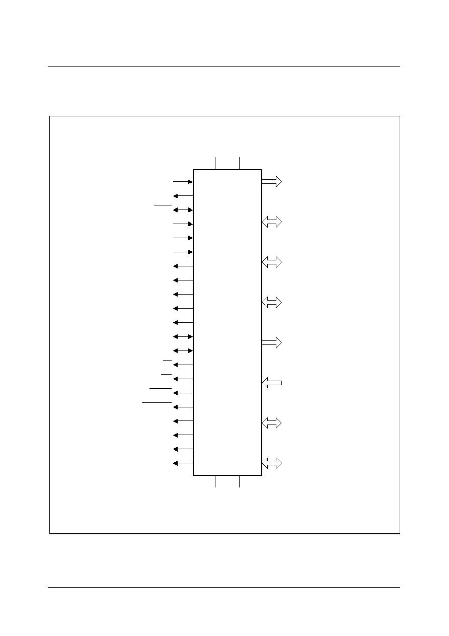
1.2
Logic Symbol
Figure 1-2
Logic Symbol
UEL11115
SS
V
DD(3.3 V)
V
XTAL1
Address
16 Bit
XTAL2
RSTIN
CVBS1A
CVBS1B
CVBS2
R
G
B
COR
BLANK
HSYNC
VSYNC
RD
WR
CSROM
CSSDRAM
MEMCLK
UDQM
LDQM
CLKEN
16 Bit
Data
Port 2
8 Bit
15 Bit
Port 3
6 Bit
Port 4
6 Bit
Port 5
7 Bit
Port 6
4 Bit
JTAG
SS
V
DD(2.5 V)
V
M2

Pin Description

SDA 6000 / SDA 6001
PRELIMINARY DATA SHEET
Version 3.00
Pin Descriptions
2 - 3
Micronas
2
Pin Descriptions
SDA 6000 / SDA 6001
PRELIMINARY DATA SHEET
Version 3.00
Pin Descriptions
2 - 4
Micronas
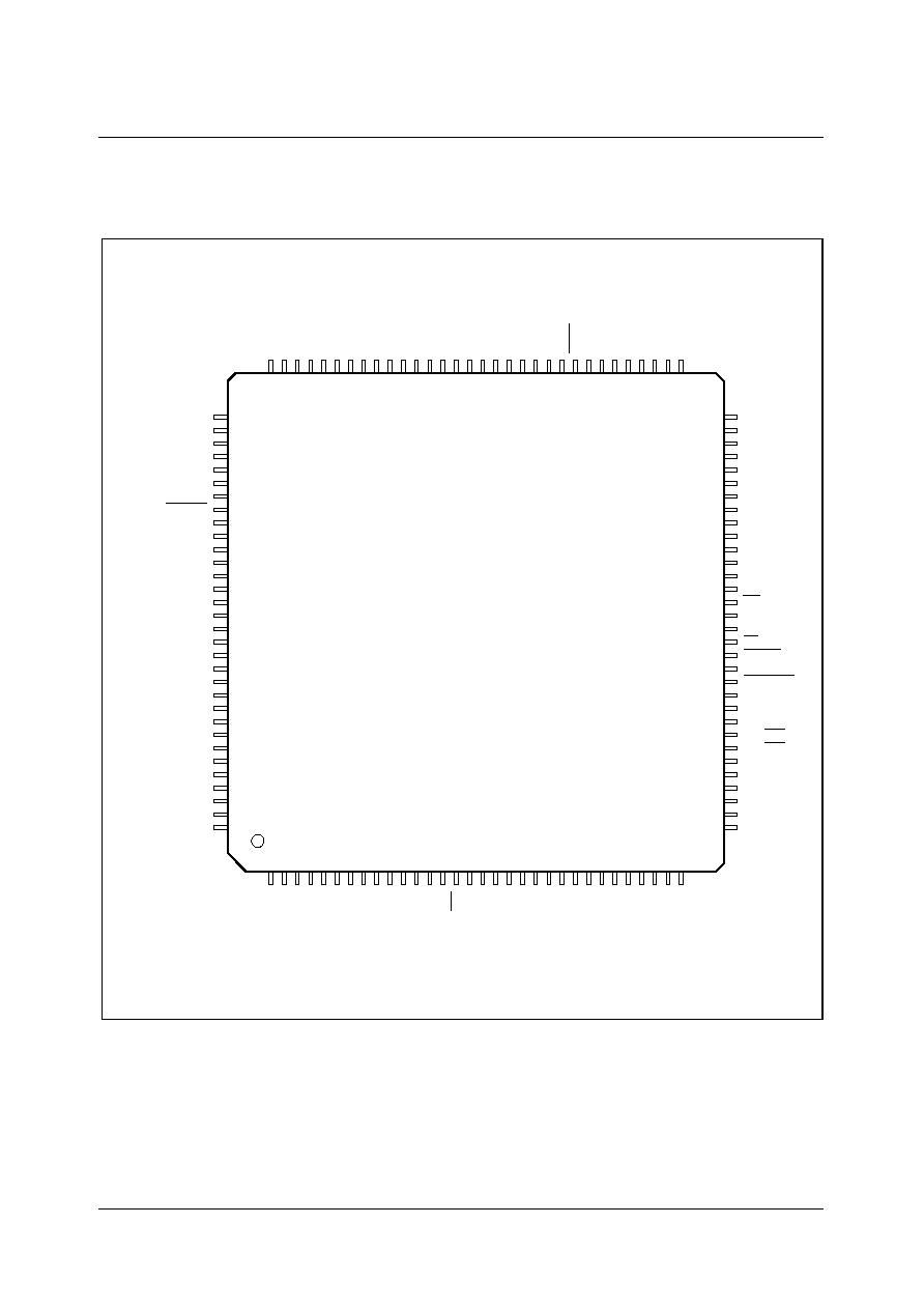
2.1
Pin Diagram (top view)
Figure 2-1
Pin Configuration
M2
V
DD33-2
UEP11116
P5.3
A3
TMODE
A4
TMS
D2
1
2
3
4
5
6
7
8
9
10
11
12
13
14
15
16
17
18
19
20
21
22
23
24
25
26
27
28
29
30
31
32
128
127
34
126
35
125
36
124
37
123
38
122
39
121
40
120
41
119
42
118
117
44
116
45
115
46
114
47
113
48
112
49
111
50
110
51
109
52
108
107
54
106
55
105
56
104
57
103
58
102
59
101
60
100
61
99
62
98
97
64
96
95
94
93
92
91
90
89
88
87
86
84
83
82
81
80
79
78
77
76
75
74
73
72
71
70
69
68
67
66
65
33
63
53
43
V
SS33-3
V
SS33-6
V
DDA-4
85
TCK
TDI
TDO
P2.8
P2.9
P2.10
P2.11
P2.12
P2.13
P2.14
P2.15
V
SS33-1
DD33-1
V
P4.5/CS3
P4.4/A20
P4.3/A19
P4.2/A18
P4.1/A17
SS25-1
V
DD25-1
V
P4.0/A16
A8
A7
A6
A5
A10
A11
A12
A9
V
SS33-2
A2
A1
A0
A13
A14/RAS
A15/CAS
DD33-3
V
MEMCLK
CSSDRAM
CLKEN
CSROM
RD
UDQM
LDQM
WR
D15
SS33-4
V
DD33-4
V
D7
D0
D14
D8
D6
D1
SS33-5
V
DD33-5
V
D5
D9
D13
D12
D10
V
DD33-6
D4
D3
D11
RSTIN
P3.0
P3.1
P3.2
P3.3
P3.4
P3.5
P3.6
P3.7
P3.8
P3.9
V
SS33-7
DD33-7
V
SS25-2
V
DD25-2
V
P3.10
P3.11
P3.12
P3.13
P3.15
P5.14
P5.15
P6.0
P6.1
P5.2
P5.1
P5.0
SSA-4
V
CVBS1A
CVBS1B
DDA-3
V
SSA-3
V
CVBS2
DDA-2
V
SSA-2
V
B
G
R
DDA-1
V
SSA-1
V
XTAL2
XTAL1
SS33-8
V
DD33-8
V
BLANK/CORBLA
COR/RSTOUT
HSYNC
VSYNC
P6.6
P6.5
P6.4
P6.3
P6.2
P-MQFP-128-2
P-MQFP-128-2

SDA 6000 / SDA 6001
PRELIMINARY DATA SHEET
Version 3.00
Pin Descriptions
2 - 5
Micronas
2.2
Pin Definitions and Functions
Table 2-1
Pin Definition and Functions
Pin
No.
Pin Name
Second
Function
Dir.
Function
37
A0
R0/C0
O
Address bit (All addresses are word
addresses)/SDRAM Address bit
36
A1
R1/C1
O
Address bit/SDRAM address bit
35
A2
R2/C2
O
Address bit/SDRAM address bit
34
A3
R3/C3
O
Address bit/SDRAM address bit
33
A4
R4/C4
O
Address bit/SDRAM address bit
27
A5
R5/C5
O
Address bit/SDRAM address bit
26
A6
R6/C6
O
Address bit/SDRAM address bit
24
A7
R7/C7
O
Address bit/SDRAM address bit
23
A8
R8
O
Address bit/SDRAM address bit
25
A9
R9
O
Address bit/SDRAM address bit
28
A10
R10
O
Address bit/SDRAM address bit
29
A11
R11
O
Address bit/SDRAM address bit
30
A12
R12
O
Address bit/SDRAM address bit
38
A13
R13
O
Address bit/SDRAM address bit
39
A14
RAS
O
Address bit/
Row address strobe for SDRAM access
40
A15
CAS
O
Address bit/
Column address strobe for SDRAM access
55
D0
�
I/O
Data bit
59
D1
�
I/O
Data bit
65
D2
�
I/O
Data bit
71
D3
�
I/O
Data bit
70
D4
�
I/O
Data bit
64
D5
�
I/O
Data bit
58
D6
�
I/O
Data bit
54
D7
�
I/O
Data bit
57
D8
�
I/O
Data bit
63
D9
�
I/O
Data bit

SDA 6000 / SDA 6001
PRELIMINARY DATA SHEET
Version 3.00
Pin Descriptions
2 - 6
Micronas
67
D10
�
I/O
Data bit
72
D11
�
I/O
Data bit
66
D12
�
I/O
Data bit
62
D13
�
I/O
Data bit
56
D14
�
I/O
Data bit
51
D15
�
I/O
Data bit
47
RD
�
O
External memory read strobe for ROM. RD is
activated for every external instruction or data
read access.
46
CSROM
�
O
Chip select signal for ROM device
44
CSSDRAM �
O
Chip select signal for SDRAM device
43
MEMCLK
�
O
Clock for SDRAM
45
CLKEN
�
O
Enable for memory clock
50
WR
�
O
Memory write strobe
22
P4.0
A16
O
General purpose output port/Address bit
19
P4.1
A17
O
General purpose output port/Address bit
18
P4.2
A18
O
General purpose output port/Address bit
17
P4.3
A19
O
General purpose output port/Address bit
16
P4.4
A20
O
General purpose output port/Address bit
15
P4.5
CS3
O
General purpose output port/Chip select
signal for second external static memory
49
LDQM
�
O
Write disable for low byte
48
UDQM
�
O
Write disable for high byte
109
XTAL2
�
O
Output of the oscillator amplifier circuit
108
XTAL1
�
I
Input of the oscillator amplifier circuit
73
RSTIN
�
I
Reset input pin
121
CVBS1A
�
I
CVBS signal inputs for full service data slicing
120
CVBS1B
�
I
Ground for CVBS1A (differential input)
117
CVBS2
�
I
CVBS signal inputs for WSS data slicing
112
R
�
O
Analog output for red channel
Table 2-1
Pin Definition and Functions (cont'd)
Pin
No.
Pin Name
Second
Function
Dir.
Function

SDA 6000 / SDA 6001
PRELIMINARY DATA SHEET
Version 3.00
Pin Descriptions
2 - 7
Micronas
113
G
�
O
Analog output for green channel
114
B
�
O
Analog output for blue channel
104
COR
RSTOUT
O
Output for contrast reduction/Reset output
105
BLANK
CORBLA
O
Fast blanking signal/Three-level signal for
contrast reduction + fast blanking
103
HSYNC
�
I/O
Horizontal sync In/output
102
VSYNC
VCS
I/O
Vertical sync In/output/Composite sync output
5
P2.8
EX0IN
I/O
General purpose I/O port/External interrupt 0
6
P2.9
EX1IN
I/O
General purpose I/O port/External interrupt 1;
see also chapter 10.8
7
P2.10
EX2IN
I/O
General purpose I/O port/External interrupt 2;
see also chapter 10.8
8
P2.11
EX3IN
I/O
General purpose I/O port/External interrupt 3;
see also chapter 10.8
9
P2.12
EX4IN
I/O
General purpose I/O port/External interrupt 4;
see also chapter 10.8
10
P2.13
EX5IN
I/O
General purpose I/O port/External interrupt 5;
see also chapter 10.8
11
P2.14
EX6IN
I/O
General purpose I/O port/External interrupt 6
12
P2.15
EX7IN
I/O
General purpose I/O port/External interrupt 7
74
P3.0
SCL0
I/O
General purpose I/O port/I
2
C Bus clock line 0
75
P3.1
SDA0
I/O
General purpose I/O port/I
2
C Bus data line 0
76
P3.2
CAPIN
I/O
General purpose I/O port/GPT2 register
CAPREL
77
P3.3
T3OUT
I/O
General purpose I/O port/GPT1 timer T3
toggle; see also chapter 10.8
78
P3.4
T3EUD
I/O
General purpose I/O port/GPT1 timer T3 ext.
up/down; see also chapter 10.8
79
P3.5
T4IN
I/O
General purpose I/O port/GPT1 timer T4 input
for count/gate/reload/capture; see also
chapter 10.8
80
P3.6
T3IN
I/O
General purpose I/O port/GPT1 timer T3
count/gate input; see also chapter 10.8
Table 2-1
Pin Definition and Functions (cont'd)
Pin
No.
Pin Name
Second
Function
Dir.
Function

SDA 6000 / SDA 6001
PRELIMINARY DATA SHEET
Version 3.00
Pin Descriptions
2 - 8
Micronas
81
P3.7
T2IN
I/O
General purpose I/O port/GPT1 timer T2 input
for count/gate/reload/capture; see also
chapter 10.8
82
P3.8
MRST
I/O
General purpose I/O port/SSC master-
receiver/slave-transmit I/O
83
P3.9
MTSR
I/O
General purpose I/O port/SSC master-
transmit/slave-receiver O/I
88
P3.10
TxD0
I/O
General purpose I/O port/ASC0 clock/data
output
89
P3.11
RxD0
I/O
General purpose I/O port/ASC0 data input
(asynchronous) or I/O (synchronous.)
90
P3.12
�
I/O
General purpose I/O port; see also chapter
10.8
91
P3.13
SCLK
I/O
General purpose I/O port/SSC master clock
output/slave clock input
92
P3.15
�
I/O
General purpose I/O port; see also chapter
10.8
124
P5.0
AN.0
I
General purpose Input port/Analog input for
A/D-converter
125
P5.1
AN.1
I
General purpose Input port/Analog input for
A/D-converter
126
P5.2
AN.2
I
General purpose Input port/Analog input for
A/D-converter
127
P5.3
AN.3
I
General purpose Input port/Analog input for
A/D-converter
93
P5.14
T4EUD
I/O
General purpose Input port/GPT1 timer T4
ext.up/down ctrl. input; see also chapter 10.8
94
P5.15
T2EUD
I/O
General purpose Input port/GPT1 timer T2
ext.up/down ctrl. input; see also chapter 10.8
95
P6.0
TRIG_IN
I/O
General purpose I/O port/Trigger input-signal
for `On Chip Debug System' (OCDS); see also
chapter 10.8
Table 2-1
Pin Definition and Functions (cont'd)
Pin
No.
Pin Name
Second
Function
Dir.
Function

SDA 6000 / SDA 6001
PRELIMINARY DATA SHEET
Version 3.00
Pin Descriptions
2 - 9
Micronas
96
P6.1
TRIG_OUT I/O
General purpose I/O port/Trigger output-
signal for `On Chip Debug System' (OCDS);
see also chapter 10.8
97
P6.2
FIELD
I/O
General purpose I/O port/Field signal of field
detection; see also chapter 10.8
98
P6.3
SCL1
I/O
General purpose I/O port/I
2
C bus clock line 1
99
P6.4
SDA1
I/O
General purpose I/O port/I
2
C bus data line 1
100
P6.5
�
I/O
General purpose I/O port
101
P6.6
SDA2
I/O
General purpose I/O port/I
2
C bus data line 2
1
TCK
�
I
Clock for JTAG interface
3
TDI
�
I
Data input for JTAG interface
4
TDO
�
O
Data output for JTAG interface
2
TMS
�
I
Control signal for JTAG interface
128
TMODE
�
I
Testmode pin
1)
110
V
SSA-1
�
S
Analog ground
111
V
DDA-1
�
S
Analog power (for PLL and DAC) (2.5 V)
115,
118,
122
V
SSA2-4
�
S
Analog ground
116,
119,
123
V
DDA2-4
�
S
Analog power (for ADCs) (2.5 V)
20, 86
V
SS25 1-2
�
S
Digital ground (for digital core)
21, 87
V
DD25 1-2
�
S
Digital power (for digital core) (2.5 V)
Table 2-1
Pin Definition and Functions (cont'd)
Pin
No.
Pin Name
Second
Function
Dir.
Function

SDA 6000 / SDA 6001
PRELIMINARY DATA SHEET
Version 3.00
Pin Descriptions
2 - 10
Micronas
13, 31,
41, 52,
60, 68,
84,
107
V
SS33 1-8
�
S
Digital ground for pads
14, 32,
42, 53,
61, 69,
85,
106
V
DD33 1-8
�
S
Digital power (for pads) (3.3 V)
1)
(Must be kept to "0" in application.)
Table 2-1
Pin Definition and Functions (cont'd)
Pin
No.
Pin Name
Second
Function
Dir.
Function

Architectural Overview
SDA 6000 / SDA 6001
PRELIMINARY DATA SHEET
Version 3.00
Architectural Overview
3 - 3
Micronas
3
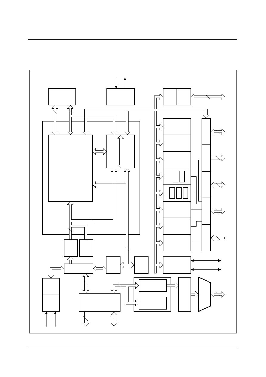
Architectural Overview
Figure 3-1
M2 Top Level Block Diagram
UEB10716
4-
Channel
ADC
7-bit
USART
ASC
SSC
SPI
GPT1
T2
T3
T4
GPT2
T5
T6
2
C
RTC
Watchdog
OCDS
JTAG
Port 5
Port 3
Port 2
Port 4
6
15
8
8
D-Sync
3
3 x 6 Bit
DAC
FIFO
SRU
GA
XRAM
Interrupt Controller
PEC
36 nodes (8 ext.)
OSC
(6 MHz)
Internal
RAM
2 Kbyte
16
16
Data
Data
Instr./Data
32
-Cache
D-Cache
16
X-BUS
Instr./Data
Interface
External
Bus
16
Slicer2
Slicer1
ACQ
16
Data
16...21
Addr.
CVBS2
CPU-Core
C166
16
16
CVBS1
HV
ROM
Boot
Port 6
7
4
2 Kbyte
XTAL
AMI

SDA 6000 / SDA 6001
PRELIMINARY DATA SHEET
Version 3.00
Architectural Overview
3 - 4
Micronas
The architecture of M2 comprises of a 16-bit microcontroller which is derived from the
well known Infineon Technologies C16x controller family. Due to the core philosophy of
M2, the architecture of the CPU core is the same as described in other Infineon
Technologies C16x derivatives.
The CPU, with its peripherals, can be used on one hand to perform all TV controlling
tasks, and on the other hand to process the data, sliced by the slicer, and the acquisition
unit according to the TTX standard. Furthermore it is used to generate an "instruction list"
for the graphic accelerator which supports the CPU by generating the display.
M2 has integrated two digital slicers for two independent CVBS signals. One slicer is
used to capture the data (e.g. Teletext or EPG) from the main channel, the other slicer
can be used to slice the WSS information from a different channel, which is helpful e.g.
to support PIP applications in 16:9 TVs. Both slicers separate the data from the analog
signal and perform the bit synchronization and framing code selection before the data is
stored in a programmable VBI buffer in the external RAM. Capturing and storing the raw
data in the RAM does not need any CPU power.
M2's display concept has improved in comparison to the common known state of the art
Teletext-ICs. The display concept is based on a pixel orientated attribute definition
instead of the former character orientated attribute definition.
For the processing of this new pixel based attribute definition the display generator
architecture is divided in two subblocks: the graphic accelerator (GA) and the screen
refresh unit (SRU).
The graphic accelerator is used to modify the frame buffer. From an abstract point of
view, the graphic accelerator is a DMA which is optimized for OSD functionality, so e.g.
bitmaps can be copied to the frame buffer. The graphic accelerator is used to draw
rectangles, parallelograms, horizontal, vertical and diagonal lines. The user does not
need to access the graphic accelerator directly, thanks to an easy to handle SW-GDI
function which is available with the M2 hardware.
The DMA functionality of the display generator (DG) supports the pixel transfer between
any address of entire external memory. The teletext and graphic capabilities can be used
simultaneously, so that M2 can combine teletext information with e.g. background
images and advanced high resolution OSD graphics.
M2 uses the frame buffer located in external memory so every bitmap can be placed at
any location on the screen. The contents of the frame buffer does not have to be set up
in real time. The duration of the set up of the screen depends on the contents of the
displayed information.
M2 supports two hardware display layers. To refresh the screen the M2 reads and mixes
two independent pixel sources simultaneously.
Different formats of the pixels which are part of different applications (e.g. Teletext
formats, 12-bit RGB or 16-bit RGB values) can be stored in the same frame buffer at the
same time.

SDA 6000 / SDA 6001
PRELIMINARY DATA SHEET
Version 3.00
Architectural Overview
3 - 5
Micronas
The screen refresh unit is used to read the frame buffer pixel by pixel in real time and to
process the transparency and RGB data. A color look up table (CLUT) can be used to
get the RGB data of the current pixel. Afterwards the RGB data is transferred to the D/A
converter. The blank signal and contrast reduction signal (COR) is also processed for
each pixel by the SRU and transferred to the corresponding output pins.
The pixel, line and field frequencies are widely programmable so that the sync system
can be used from low end 50 Hz to high end 100 HZ TV applications as well as for any
other standard.
The on chip clock system provides the M2 with its basic clock signals. Independent
clock domains are provided for the embedded controller, the bus interface and the
display system. The pixel clock can vary between 10 MHz and 50 MHz.
Due to the unified memory architecture of M2, a new bus concept is implemented. An
arbiter handles the bus requests from the different request sources. These are:
� Slicer 1 requests (normally used as a TTX slicer)
� Slicer 2 requests (used as a WSS slicer)
� Graphic accelerator requests
� Screen refresh unit requests
� Data requests from the CPU via XBUS
� Instruction requests via the CPU program bus
For exploiting the full computational power of the controller core the code of time critical
routines can be stored in one bank of the external SDRAM separated from all display
information (frame buffer, character set etc.). An instruction cache (I-CACHE) is used
for buffering instruction words in order to minimize the probability of wait states to occur
when the microcontroller is interfering with the display generator (DG) for access rights
to the external memory devices. The data cache (D-CACHE) serves for operand reads
and writes via the XBUS from/to external memory devices.
The external bus interface (EBI) features interleaved access cycles to one or two static
external memory devices (ROM, Flash-ROM or SRAM) with a total maximum size of
4 MByte and one PC100 compliant (Intel standard) SDRAM device (16 MBit organized
as 2 memory banks or 64 MBit organized as 4 memory banks).
For TV controlling tasks M2 provides three serial interfaces (I
2
C, ASC, SSC), two general
purpose timers, (GPT1, GPT2), a real time clock (RTC), a watch dog timer (WDT), an A/
D converter and eight external interrupts.

C16X Microcontroller

SDA 6000 / SDA 6001
PRELIMINARY DATA SHEET
Version 3.00
C16X Microcontroller
4 - 3
Micronas
4
C16X Microcontroller

SDA 6000 / SDA 6001
PRELIMINARY DATA SHEET
Version 3.00
C16X Microcontroller
4 - 4
Micronas
4.1
Overview
M2's microcontroller and its peripherals are based on a Cell-Based Core (CBC) which is
compatible to the well known C166 architecture.
In M2, the CPU and its peripherals are generally clocked with 33.33 MHz which results
in an instruction cycle time of 60 ns. The implementation of the microcontroller within M2
deviates from other known C16x derivates since the controller's XBUS is not used as the
external bus. All external access cycles of the microcontroller, the display generator and
the acquisition unit are performed via a high performance time interlocking SDRAM bus.
The external bus interface (EBI) manages the arbitration procedure for access cycles to
the external synchronous DRAM in parallel to an external static memory (ROM or
FLASH; for more details refer to Chapter 4.4).
Due to the realtime critical bus bandwidth requirements of the display generator,
unpredictable wait-states for the controller may occur. These wait-states do not destroy
the overall average system performance, because they are mostly buffered by the CPU
related instruction and data buffers. Nevertheless they can influence, for example, the
worst disconnection response time.
Emulation is now performed by an on-chip debug module which can be accessed by a
JTAG interface.
The following microcontroller peripherals are implemented:
� 2 KByte IRAM (System RAM)
� 2 KByte XRAM (XBUS located)
� 32 Interrupt Nodes
� General Purpose Timer Units (GPT1 and GPT2)
� Real Time Clock (RTC)
� Asynchronous/Synchronous Serial Interface (ASC0)
� High-Speed Synchronous Serial Interface (SSC)
� I
2
C Bus Interface (I
2
C)
� 4-Channel 8-bit A/D Converter (ADC)
� Watchdog Timer (WDT)
� On-Chip Debug Support Module (OCDS)
� 42 Multiple Purpose Ports
Central Processing Unit
The CPU executes the C166 instruction set (with the extensions of the C167 products).
Its main features are the following:
� 4-stage pipeline (Fetch, Decode, Execute and Write-Back).
� 16
�
16-bit General Purpose Registers
� 16-bit Arithmetic and Logic Unit
� Barrel shifter
� Bit processing capability

SDA 6000 / SDA 6001
PRELIMINARY DATA SHEET
Version 3.00
C16X Microcontroller
4 - 5
Micronas
� Hardware support for multiply and divide instructions
Internal RAM (IRAM)
The internal dual-port RAM is the physical support for the General Purpose Registers,
the system stack and the PEC pointers. Due to its close connections with the CPU, the
internal RAM provides fast access to these resources. As the GPR bank can be mapped
anywhere in the internal RAM through a base pointer (Context Pointer CP), fast context
switching is allowed. The internal RAM is mapped in the memory space of the CPU and
can be used also to store user variables or code.
Interrupt Controller
Up to 32 interrupt sources can be managed by the Interrupt Controller through a multiple
priority system which provides the user with the ability to customize the interrupt
handling.
The interrupt system of M2 includes a Peripheral Event Controller (PEC). This processor
performs single-cycle interrupt-driven byte or word transfers between any two locations
in the entire memory space of M2.
In M2, the PEC functionalities are extended by the External PEC which allows an
external device to trigger a PEC transfer while providing the source and destination
pointers. New features also include the packet transfer mode and the channel link mode.
Besides user interrupts, the Interrupt Controller provides mechanisms to process
exceptions or error conditions, so-called "hardware traps", that arise during program
execution.
System Control Unit
M2's System Control Unit (CSCU) is used to control system specific tasks such as reset
control or power management within an on-chip system built around the core. The power
management features of the CSCU provide effective means to realize standby
conditions for the system with an optimum balance between power reduction, peripheral
operation and system functionality. The CSCU also provides an interface to the Clock
Generation Unit (CGU) and is able to control the operation of the Real Time Clock (RTC).
The CSCU includes the following functions:
� System configuration control
� Reset sequence control
� External interrupt and frequency output control
� Watchdog timer module
� General XBUS peripherals control
� Power management additional to the standard Idle and Power Down modes
� Control interface for Clock Generation Unit
� Identification register block for chip and CSCU identification

SDA 6000 / SDA 6001
PRELIMINARY DATA SHEET
Version 3.00
C16X Microcontroller
4 - 6
Micronas
OCDS
The On-Chip Debug System allows the detection of specific events during user program
execution through software and hardware breakpoints. An additional communication
module allows communication between the OCDS and an external debugger, through a
standard JTAG port. This communication is performed in parallel to program execution.

SDA 6000 / SDA 6001
PRELIMINARY DATA SHEET
Version 3.00
C16X Microcontroller
4 - 7
Micronas
4.2
Memory Organization
In normal operation mode the memory space of the CPU is configured in a "Von
Neumann" architecture. This means that code and data are accessed within the same
memory areas, i. e. external memory, internal controller memory (IRAM), the address
areas for integrated XBUS peripherals (I
2
C, internal XBUS memory (XRAM)) and the
special function register areas (SFR, ESFR) are mapped into one common address
space of 16 MBytes. This address space is arranged as 256 segments of 64 KBytes
each and each segment is again subdivided into four data pages of 16 KBytes each.
All internal memory areas and the address space of the integrated XBUS peripherals are
mapped to segment 0. Code and data may be stored in any part of the memory, except
for the SFR blocks, which can not be used for instructions. Despite this equivalence of
code and data, proper partitioning is necessary to make use of the full bandwidth of the
memory system.
The integrated C16x controller communicates via 2 busses with the memory interface.
In normal operation mode access to segments 00
H
to 41
H
(excluding internal memory
areas) is mapped to the read only program memory bus (PMBUS), whereas access to
segments 42
H
to FF
H
is mapped to the XBUS. In bootstrap loader mode (BSLMode)
instruction fetches to external memory areas via PMBUS are redirected to the internal
bootstrap loader ROM (BSLROM). Operand (data) accesses remain unchanged.
The PMBUS is connected to the instruction cache (ICACHE) which operates as read-
ahead FIFO (see Figure 4-1). The data cache (DCACHE) which is connected to the
XBUS holds a maximum of 4 words corresponding to one SDRAM burst. Accesses of
DCACHE, ICACHE and the acquisition unit (ACQ) are joined within the acquisition
memory interface (AMI) and directed to the external bus interface (EBI). Redirections via
ESFR REDIR and ESFR REDIR1 are done in the AMI (see Chapter 4.5.1). The EBI
joins AMI and display generator (DG) accesses and reads data from or writes data to the
external static and dynamic memory devices (see Chapter 4.5 for further information).
In case of cache miss wait states are inserted until the data is ready. IRAM, XRAM and
the special function register areas can be accessed without wait states.
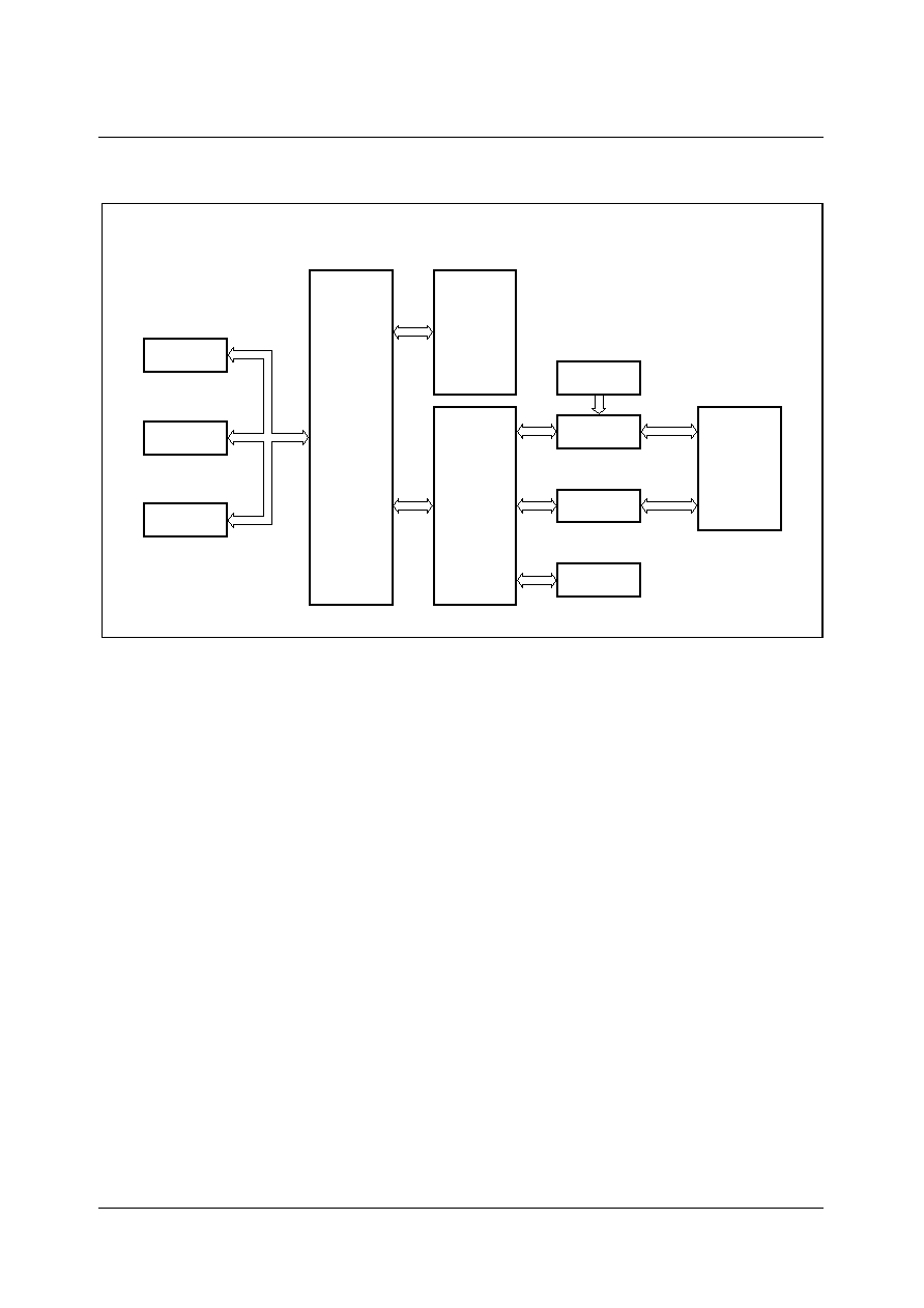
SDA 6000 / SDA 6001
PRELIMINARY DATA SHEET
Version 3.00
C16X Microcontroller
4 - 8
Micronas
Figure 4-1
M2 Memory Path Block Diagram
All memory locations are byte and word readable. The internal memories (IRAM, XRAM)
and the external dynamic memory (SDRAM) are byte and word writable, but external
static memory is only word writable. Bytes are stored at even or odd byte addresses.
Words are stored in ascending memory locations, with the low byte at an even byte
address being followed by the high byte at the next odd byte address. Double words
(instructions only) are stored in ascending memory locations as two subsequent words.
Single bits are always stored in the specific bit position at a word address. Bit position 0
is the least significant bit of the byte at an even byte address and bit position 15 is the
most significant bit of the byte at the next odd byte address. Bit addressing is supported
by a part of the special function registers, a part of the IRAM and the general purpose
registers (GPRs).
UED11214
SDRAM
ROM1
ROM2
EBI
AMI
ICACHE
DCACHE
ACQ
C16X
Boot ROM
DG
PMBUS
XBUS
Memory
External
M2

SDA 6000 / SDA 6001
PRELIMINARY DATA SHEET
Version 3.00
C16X Microcontroller
4 - 9
Micronas
Figure 4-2
Storage of Words, Byte and Bits in a Byte Organized Memory
Note: Byte units forming a single word or a double word must always be stored within
the same physical (internal, external, ROM, RAM) and organizational (page,
segment) memory area.

SDA 6000 / SDA 6001
PRELIMINARY DATA SHEET
Version 3.00
C16X Microcontroller
4 - 10
Micronas
4.3
On-Chip Microcontroller RAM and SFR Area
The IRAM/SFR area is located within data page 3, and provides access to 2 KByte of
dual ported IRAM and two 512 Byte blocks of Special Function Registers (SFRs).
The internal RAM (IRAM) serves several purposes:
� System Stack (Programmable Size)
� General Purpose Register Banks (GPRs)
� Source and Destination Pointers for the Peripheral Event Controller (PEC)
� Variable and other data storage, or
� Code storage
Figure 4-3
Internal RAM Areas and SFR Areas
Note: The upper 256 bytes of SFR area, ESFR area and IRAM are bit-addressable (see
shaded blocks in Figure 4-3).
UED11213
00'8000
00'0000
H
Page 0
H
00'4000
H
Page 1
00'F600
00'F000
00'F200
ESFR Area
Reserved
H
H
H
RAM / SFR Area
64 Kbytes
Segment 0
00'C000
H
Page 2
Page 3
00'F000
H
00'FFFF
H
00'FFFF
00'FA00
00'FE00
2 Kbyte
IRAM
RAM / SFR Area
4 Kbytes
SFR Area
H
H
H
XRAM
00'E800
H
00'E000
H
2
C

SDA 6000 / SDA 6001
PRELIMINARY DATA SHEET
Version 3.00
C16X Microcontroller
4 - 11
Micronas
Code accesses are always made through even byte addresses. The highest possible
code storage location in the IRAM is either 00'FDFE
H
for single word instructions, or
00'FDFC
H
for double word instructions. The respective location must contain a branch
instruction (unconditional), because sequential boundary crossings from IRAM to the
SFR area are not supported and cause erroneous results.
Any word and byte data in the IRAM can be accessed via indirect or long 16-bit
addressing modes if the selected DPP register points to page 3. Any word data access
is made through an even byte address. The highest possible word data storage location
in the IRAM is 00'FDFE
H
. For PEC data transfers, the IRAM can be accessed
independent of the contents of the DPP registers via the PEC source and destination
pointers.
The upper 256 Byte of the IRAM (00'FD00
H
through 00'FDFF
H
) and the GPRs of the
current bank are provided for single bit storage, and thus they are bit addressable.
4.3.1
System Stack
The system stack may be defined within the IRAM. The size of the system stack is
controlled by bit field STKSZ in the SYSCON register (see table below).
For all system stack operations, the IRAM is accessed via the Stack Pointer (SP)
register. The stack grows downward from higher to lower RAM address locations. Only
word accesses are supported by the system stack. A stack overflow (STKOV) and a
stack underflow (STKUN) register are provided to control the lower and upper limits of
the selected stack area. These two stack boundary registers can be used not only for
protection against data destruction, but also to implement flushing and filling a circular
stack with a hardware supported system stack (except for option `111').
<STKSZ>
Stack Size
(Words)
Internal RAM Addresses (Words)
0 0 0
B
256
00'FBFE
H
... 00'FA00
H
(Default after Reset)
0 0 1
B
128
00'FBFE
H
... 00'FB00
H
0 1 0
B
64
00'FBFE
H
... 00'FB80
H
0 1 1
B
32
00'FBFE
H
... 00'FBC0
H
1 0 0
B
512
00'FBFE
H
... 00'F800
H
1 0 1
B
�
Reserved. Do not use this combination.
1 1 0
B
�
Reserved. Do not use this combination.
1 1 1
B
1024
00'FDFE
H
... 00'F600
H
(Note: No circular stack)

SDA 6000 / SDA 6001
PRELIMINARY DATA SHEET
Version 3.00
C16X Microcontroller
4 - 12
Micronas
4.3.2
General Purpose Registers
The General Purpose Registers (GPRs) use a block of 16 consecutive words within the
IRAM. The Context Pointer (CP) register determines the base address of the currently
active register bank. This register bank may consist of up to 16 word GPRs (R0, R1, ...,
R15) and/or of up to 16 byte GPRs (RL0, RH0, ..., RL7, RH7). The sixteen byte GPRs
are mapped onto the first eight word GPRs (see Table 4-1).
In contrast to the system stack, a register bank grows from lower towards higher address
locations and occupies a maximum space of 32 Byte. The GPRs are accessed via short
2-, 4- or 8-bit addressing modes using the Context Pointer (CP) register as a base
address (independent of the current DPP register contents). In addition, each bit in the
currently active register bank can be accessed individually.
M2 supports fast register bank (context) switching. Multiple register banks can physically
exist within the IRAM at the same time. However, only the register bank selected by the
Context Pointer register (CP) is active at a given time. Selecting a new active register
bank is simply done by updating the CP register. A particular Switch Context (SCXT)
instruction performs register bank switching and automatically saves the previous
Table 4-1
Mapping of General Purpose Registers to RAM Addresses
Internal RAM
Address
Byte Registers
Word Register
<CP> + 1E
H
�
R15
<CP> + 1C
H
�
R14
<CP> + 1A
H
�
R13
<CP> + 18
H
�
R12
<CP> + 16
H
�
R11
<CP> + 14
H
�
R10
<CP> + 12
H
�
R9
<CP> + 10
H
�
R8
<CP> + 0E
H
RH7
RL7
R7
<CP> + 0C
H
RH6
RL6
R6
<CP> + 0A
H
RH5
RL5
R5
<CP> + 08
H
RH4
RL4
R4
<CP> + 06
H
RH3
RL3
R3
<CP> + 04
H
RH2
RL2
R2
<CP> + 02
H
RH1
RL1
R1
<CP> + 00
H
RH0
RL0
R0
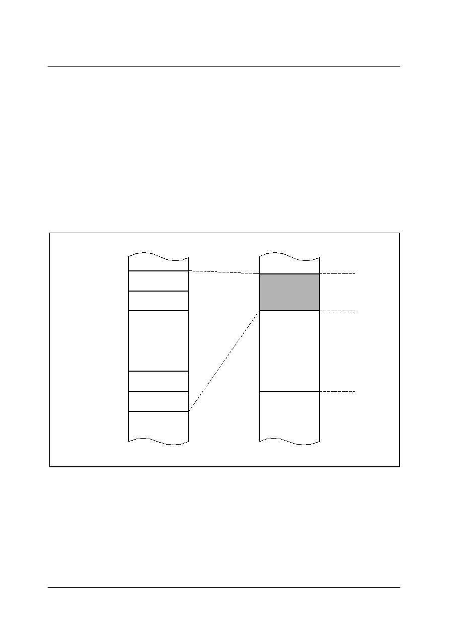
SDA 6000 / SDA 6001
PRELIMINARY DATA SHEET
Version 3.00
C16X Microcontroller
4 - 13
Micronas
context. The number of implemented register banks (arbitrary sizes) is only limited by the
size of the available internal RAM.
4.3.3
PEC Source and Destination Pointers
The 16 word locations in the IRAM from 00'FCE0
H
to 00'FCFE
H
(just below the bit-
addressable section) are provided as source and destination offset address pointers for
data transfers on the eight PEC channels. Each channel uses a pair of pointers stored
in two subsequent word locations, with the source pointer (SRCPx) on the lower and the
destination pointer (DSTPx) on the higher word address (x = 7 ... 0). In M2, these
pointers are used to specify the address offset within the segment, and the destination /
source segment numbers are specified in designated SFRs (see Chapter 5.2).
Figure 4-4
Location of the PEC Pointers
Whenever a PEC data transfer is performed, the pair of source and destination pointers,
which is selected by the specified PEC channel number, is accessed independent of the
current DPP register contents; the locations referred to by these pointers are also
accessed independent of the current DPP register contents. If a PEC channel is not
used, the corresponding pointer locations are available and can be used for word or byte
data storage.
00'FCE2
00'FCE0
H
H
SRCP0
DSTP0
00'F5FE
00'F600
MCD02266
H
H
Destination
00'FCFC
Pointers
and
H
PEC
Source
SRCP7
00'FCFE
H
DSTP7
Internal
00'FCE0
00'FDDE
RAM
H
H
00'FCFE
00'FD00
H
H

SDA 6000 / SDA 6001
PRELIMINARY DATA SHEET
Version 3.00
C16X Microcontroller
4 - 14
Micronas
4.3.4
Special Function Registers
The so-called Special Function Registers (SFRs) are provided to control internal
functions of M2 (CPU, bus interface, Interrupt Controller, OCDS) or peripherals
connected to the Peripheral Bus. These SFRs are arranged within two areas of
512 Bytes each. The first register block, the SFR area, is located in the 512 Bytes above
the internal RAM (00'FFFF
H
... 00'FE00
H
); the second register block, the Extended SFR
(ESFR) area, is located in the 512 Bytes below the IRAM (00'F1FF
H
... 00'F000
H
).
Special function registers can be addressed via indirect and long 16-bit addressing
modes. Using an 8-bit offset together with an implicit base address allows word SFRs
and their respective low bytes to be addressed. However, this does not work for the
respective high bytes!
Note: Writing to any byte of an SFR causes the non-addressed complementary byte to
be cleared!
The upper half of each register block is bit-addressable, so the respective control/status
bits can directly be modified or checked using bit addressing.
When accessing registers in the ESFR area using 8-bit addresses or direct bit
addressing, an Extend Register (EXTR) instruction is first required to switch the short
addressing mechanism from the standard SFR area to the Extended SFR area. This is
not required for 16-bit and indirect addresses. The GPRs R15 ... R0 are duplicated, i.e.
they are accessible within both register blocks via short 2-, 4- or 8-bit addresses without
switching.
ESFR_SWITCH_EXAMPLE:
EXTR
#4
;Switch to ESFR area for next 4 instr.
MOV
ODP2, #data16
;ODP2 uses 8-bit reg addressing
BFLDL
DP6, #mask, #data8
;Bit addressing for bit fields
BSET
DP1H.7
;Bit addressing for single bits
MOV
T8REL, R1
;T8REL uses 16-bit mem address,
;R1 is duplicated into the ESFR space
;(EXTR is not required for this access)
;----
;-------------------
;The scope of the EXTR #4 instruction...
; ... ends here!
MOV
T8REL, R1
;T8REL uses 16-bit mem address,
;R1 is accessed via the SFR space
In order to minimize the use of the EXTR instructions the ESFR area primarily holds
registers which are required mainly for initialization and mode selection. Registers that
need to be accessed frequently are allocated, wherever possible, to the standard SFR
area.

SDA 6000 / SDA 6001
PRELIMINARY DATA SHEET
Version 3.00
C16X Microcontroller
4 - 15
Micronas
Note: The tools are equipped to monitor accesses to the ESFR area and will
automatically insert EXTR instructions or issue a warning in case of missing or
excessive EXTR instructions.
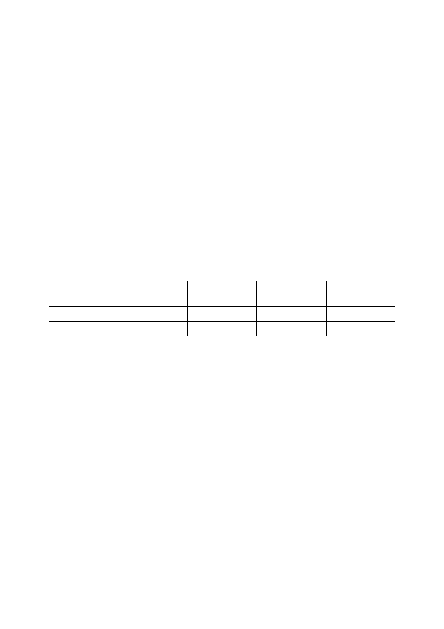
SDA 6000 / SDA 6001
PRELIMINARY DATA SHEET
Version 3.00
C16X Microcontroller
4 - 16
Micronas
4.4
External Memory
M2 provides an external bus interface (EBI) to access an external SDRAM, together with
an external static memory device (ROM or SRAM). To optimize the overall system
performance, access to both memory types is interlocked. Because of high performance
requirements M2 provides only one bus type (Demultiplexed 16-bit Bus). Depending on
the reset configuration (refer to Chapter 6.1) an external ROM/SRAM size from
128 KByte up to 4 MByte can be chosen. Although external addresses (represented by
pins A0 ... A20) are always word addresses, byte accesses to the SDRAM are possible
by using mask signals LDQM and UDQM.
4.4.1
SDRAM
PC SDRAM compliant (Intel standard) memory devices with 2 or 8 MByte and a
minimum clock period of 10 ns (latency 3) may be connected to M2's external memory
bus.
Supported data organizations are given below:
The external SDRAM connected to M2 is a multifunctional, byte or word addressable
device which can be used for frame buffers, character sets, pixel graphics, acquisitions,
microcontroller workspace and any other data storage purposes.
Using a 100 MHz external memory bus the theoretical optimum memory bandwidth is
limited to 200 MByte/s. In order to keep the sustainable memory bandwidth as close to
the optimum as possible, the bank oriented architecture of SDRAM devices has to be
exploited. Basically, display related information should be separated from controller
related data items.
The following allocation is recommended for a 2 bank, 2 MByte device:
� "Display Bank": Both Frame Buffers, Character Set, Pixel Graphic, Graphic
Accelerator Instructions (GAI), Application Data (i.e. TTX, EPG, ...)
� "Controller Bank": Instruction Code, VBI-buffer, Application Data (i.e. TTX, EPG, ...)
The suggested allocation leads to best performance results since it reduces the number
of time consuming row commands on the SDRAM.
4.4.2
External Static Memory Devices
M2 supports access to external ROM, Flash ROM and SRAM devices which provide a
read cycle time
t
RC
< 120 ns. Only 16-bit word access is supported. The maximum
Memory Size
# SDRAM
Banks
# Bank
Addresses
# Row
Addresses
# Column
Addresses
2 MByte
2
1
11
8
8 MByte
4
2
12
8

SDA 6000 / SDA 6001
PRELIMINARY DATA SHEET
Version 3.00
C16X Microcontroller
4 - 17
Micronas
memory size is limited by the number of external address lines. Up to 21 external
address lines are configurable, thus devices providing up to 4 MByte of static external
memory can be connected to M2.
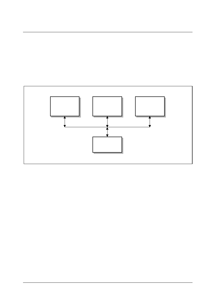
SDA 6000 / SDA 6001
PRELIMINARY DATA SHEET
Version 3.00
C16X Microcontroller
4 - 18
Micronas
4.5
External Bus Interface (EBI).
The EBI handles access channels to four SDRAM banks within one SDRAM device and
up to two static memory devices at 100 MHz. (For lower requirements the clock
frequency can be reduced to 66 MHz, refer to Chapter 8). A maximum of three external
memory devices is supported.
Figure 4-5 shows the possible configurations.
Figure 4-5
External Memory Configuration
The interlocking execution of access cycles to different memory modules is supported.
All external SDRAM access cycles must be executed with a pre-defined burst length
BL = 4 and latency 3. Write access cycles, which modify less than four SDRAM
locations, are achieved by activating mask control signals L/UDQM.
The integrated refresh controller of the EBI checks for the compliance of refresh periods
and executes refresh operations on the SDRAM devices. The refresh period can be
adapted to different SDRAm types and different bus clock frequencies by setting register
EBIREF. The configuration of different external SDRAM types can be controlled by a
special SW driver as well as refresh modes and power down features. The
microcontroller and the acquisition unit use a common interface to the EBI. A separate
connection to the EBI is provided for the display generator. The EBI performs an
arbitration procedure for granting right access to either of the request sources. But
granting right access to one source does not exclude requests initiated by the other
source from being served. A maximum of two access requests from a source may be
served consecutively if the other source is addressing an SDRAM location. Up to four
consecutive access cycles from the same source are served if the other source is
addressing an external ROM device.
UEB11118
or
M2
ROM
Flash-ROM
(2...4 banks)
2...8 MByte
SDRAM
Flash-ROM
ROM
or
128 KByte...4 MByte
128 KByte...4 MByte

SDA 6000 / SDA 6001
PRELIMINARY DATA SHEET
Version 3.00
C16X Microcontroller
4 - 19
Micronas
The following figures show typical timing diagrams that may be observed on the external
bus. The first figure presents the interlocked execution of access cycles to the external
ROM and a SDRAM device. The other figure resumes the situation when both sources
address locations are in different SDRAM banks. Detailed timings and the specification
of setup and hold conditions can be found in Chapter 14.
Figure 4-6
Interlocked Access Cycles to ROM and SDRAM
ROM_Adr
RD
CSROM
D(15:0)
A(21:0)
SDRAM Data
ca
ROM Data
ra
UET11119
ra
Read
CAS
WR
RAS
MEMCLK
CSSDRAM
Act
Write

SDA 6000 / SDA 6001
PRELIMINARY DATA SHEET
Version 3.00
C16X Microcontroller
4 - 20
Micronas
Figure 4-7
Interlocked Access Cycles to two SDRAM Banks
4.5.1
Memory Mapping
Mapping of memory locations from the address space of the C16x to physical addresses
(and chip selects) occurs in 4 steps (all addresses shown below are byte addresses
unless otherwise noted). Figure 4-8 gives a coarse depiction (without redirection) of the
mapping process in normal operation mode.
UET11120
MEMCLK
Pre
Act
Act
Pre
Act
Read
Read
Read
Read
RAS
CAS
SDRAM: 16 MBit, 2 Banks
ra
ca
ca
ra
ca
ra
ra
ra
ra
A (9:0)
A10
A11
b1
b1
b1
b1
b1
b1
b0
SDRAM: 64 MBit, 4 Banks
A10
A (9:0)
ca
ra
ra
ca
ra
ra
ca
ra
ra
ra
ra
ra
A11
A(13:12)
by
by
by
by
bx
bx by
by
D(15:0)
7
6
8
1
2
3
4
1
2
3
4
6
5
7
8
1
zo
Bank 1
Bank 0
Bank Y
Bank X
b0
Precharge
Activate
Activate
Precharge
Activate
dx
dy
dx
dy

SDA 6000 / SDA 6001
PRELIMINARY DATA SHEET
Version 3.00
C16X Microcontroller
4 - 21
Micronas
Figure 4-8
Memory Mapping
from C16x address-space to EBI address-space for 1 64MBit SDRAM (D)
and 2 16MBit static memory devices (S1, S2) is shown on the left (XBUS/
PMBUS overlap). The right part shows the mapping for 1 64MBit SDRAM
(D) and 2 32MBit static memory devices (S1, S2) (no XBUS/PMBUS
overlap). Redirection via REDIR/REDIR1 is not shown. The exclusion of the
address space for internal memories B leads to 1 segment in physical
memory that is either addressable only via PMBUS A or not addressable at
all C. To get access to these segments use REDIR1.
a) Internal mapping of the C16x:
Access to segments 0 to 64 selects the PMBUS. The address range (00'0000
H
...
40'FFFF
H
) is mapped to the range 00'0000
H
... 3F'FFFF
H
shown to the ICACHE,
thus omitting the internal memories, the special function register areas and the
XBUS peripheral address space contained the range 00'8000
H
... 01'7FFF
H
:
� C16x addresses
00'0000
H
... 00'7FFF
H
are mapped to 00'0000
H
... 00'7FFF
H
� C16x addresses
01'8000
H
... 40'FFFF
H
are mapped to 00'8000
H
... 3F'FFFF
H
41'0000
H
40'0000
H
00'0000
41'0000
H
PMBUS
H
40'0000
00'0000
01'8000
H
S1
UED11212
H
C
H
H
Address-Space
80'0000
60'0000
H
H
S1
S2
D
FF'FFFF
H
EBI
41'0000
XBUS
Address-Space
C16X
FF'FFFF
80'0000
S2
D
EBI
Address-Space
H
H
A
B
00'8000
H

SDA 6000 / SDA 6001
PRELIMINARY DATA SHEET
Version 3.00
C16X Microcontroller
4 - 22
Micronas
Access to segments 65 to 255 selects the XBUS. This address range (41'0000
H
...
FF'FFFF
H
) is not remapped by the C16x.
b) Mapping by caches:
In normal operation mode the address requested by the controller is not altered by
ICACHE and DCACHE. In bootstrap loader mode, instruction fetches via the
ICACHE are mapped to the boot ROM by the ICACHE:
� Address is mapped to
address mod 40
H
Operand reads via ICACHE and all accesses via DCACHE are passed unaltered to
the AMI.
c) Mapping and redirection in AMI:
Address mapping in AMIdepends on the settings of the ESFRs REDIR and REDIR1
as well as on the total amount of static memory. The mapping is done in the
following order:
1) Check for redirection via REDIR1: If the requested address lies in segment 255
the segment address is replaced by the low byte of REDIR1.
2) Check for redirection via REDIR: If the address resulting from step1 lies in the
address range specified by REDIR, the address is shifted to SDRAM area:
� Address is mapped to
80'0000
H
+ address � REDIR_LOWER
�
16 kBytes
3) If the total amount of static memeory in 4 MBytes or less (i.e. SALSEL
"111"
or SALSEL = "111" and no second device present) and the address resulting from
step 2 is below 4 MBytes the address is shifted by 4 MBytes:
� Address is mapped to
address + 40'0000
H
This means that the address ranges 02'0000
H
... 40'FFFF
H
(PMBUS) and 41'0000
H
... 7F'FFFF
H
(XBUS) in the address space of the C16x are mapped to the same
physical memory. The overlap allows to make use of 2 independent busses for
code (PMBUS) and data (XBUS) for fast parallel access.
If the total amount of static memory is 8 MBytes (i.e. SALSEL = "111" and a second
device is present) no further mapping occurs.
d) Mapping to addresses of specific physical devices by EBI:
1) dynamic memory:
� addresses 80'0000
H
... FF'FFFF
H
(9F'FFFF
H
) access the 64MBit (16 MBit) SDRAM
(CSSDRAM)
2) static memory:
In the total amount of static memory is 4 MBytes or less (see above) the requests
of the AMI or the DG in the address range 40'0000
H
... 7F'FFFF
H
are passed to the
external static memory devices according to the SALSEL and CSENA settings (see
Chapter 6.1). The address range 00'0000
H
... 3F'FFFF
H
must not be used. If the
total amount of the static memory is 8 MBytes there is no reserved address range:
SDA 6000 / SDA 6001
PRELIMINARY DATA SHEET
Version 3.00
C16X Microcontroller
4 - 23
Micronas
� Addresses 00'0000
H
... 3F'FFFF
H
access the first static memory device (CSROM)
� Addresses 40'0000
H
... 7F'FFFF
H
access the second static memory device (CS3)
The addresses shown on the external address lines of M2 are word oriented,
starting at 0 for each device.
The External Bus Interface (EBI) provides a special mode, the "EBI direct mode", where
the control pins to the SDRAM device are directly controlled by the CPU while the HW
finite state machines of the EBI are bypassed. "EBI direct mode" is used for
accomplishing operations on the SDRAM such as the execution of the requisite
initialization sequence, power down mode entry/exit etc. When executing a direct mode
command the EBI shifts the contents of register EBIDIR into the SDRAM control lines.
The Micronas SDRAM driver (refer to document list) provides appropriate functions for
executing operations in direct mode.
4.5.2
Register Description
Access cycles to addresses specified by bit fields REDIR_LOWER and REDIR_UPPER
are redirected by hardware to the SDRAM area. The area to which the specified range
is mapped, starts at the base address (80'0000
H
) of the SDRAM. The range for
redirection is selected in groups of 16 KByte. Using the REDIR register, access cycles
to ROM located routines may be redirected to copies of these routines in the SDRAM.
REDIR Reset
Value:
0000
H
To gain access to memory areas covered by the read only PMBUS or to areas not
accessible at all (see Figure 4-8) accesses to segment 255 can be redirected to any
other segment in EBI address space.
Bit
Function
REDIR_LOWER
(7:0)
Base address of selected range in the ROM Area
Bitfield REDIR_LOWER specifies the MSBs of the base address of
the selected range.
REDIR_UPPER
(7:0)
Upper address of selected range in the ROM Area (exclusive)
Bitfield REDIR_UPPER specifies the MSBs of the first no longer
redirected 16 KBytes.
5
4
3
2
1
0
11
10
9
8
7
6
15
14
13
12
rw
rw
REDIR_UPPER (7:0)
REDIR_LOWER (7:0)

SDA 6000 / SDA 6001
PRELIMINARY DATA SHEET
Version 3.00
C16X Microcontroller
4 - 24
Micronas
REDIR1
Reset Value: 00FF
H
The configuration of the "External Bus Interface" and its operation mode is defined with
the EBICON and EBIREF register.
Bit
Function
REDIR1_SEG
(7:0)
For access to segment 255, the segment part of the address is
replaced by REDIR1_SEG.
5
4
3
2
1
0
11
10
9
8
7
6
15
14
13
12
rw
-
REDIR1_SEG (7:0)

SDA 6000 / SDA 6001
PRELIMINARY DATA SHEET
Version 3.00
C16X Microcontroller
4 - 25
Micronas
EBIREF
Reset Value: 03E8
H
Bit
Function
EBIREF
EBI Refresh Cycles
EBIREF controlls the refresh controller for external SDRAM refresh of
the SDA6000. After EBIREF clock cycles of the SDRAM clock a new
refresh command is inserted into the command queue of the EBI and
executed with highest priority:
Refresh Cycle = EBIREF[10..0] x SDRAM
CLOCK
The reset value corresponds to 1000 * 15ns = 15�s at the starting clock
frequency of 66MHz. In order to retain the best possible performance,
EBIREF may be adapted to 0x5DC=1500 when switching to 100MHz
(1500 * 10ns = 15�s). The refesh rate may be adapted from almost 0�s
to more than 30�s. Please note that using higher refresh rates will
degrade the performance and may even block the whole system
(refresh commands are execute with highest priority) for extremly high
refresh rates (i.e. very low values of EBIREF).
Recommended EBIREF settings for different SDRAM sizes are:
SDRAM size Refresh Cycle Time Recommended setting (EBIREF)
100MHz (SDRAM
CLOCK
) 66MHz (SDRAM
CLOCK
)
16 MBit 15,6�s 1559 1039
64 MBit 15,6�s 1559 1039
128 MBit 15,6�s 1559 1039
256 MBit 7,8�s 779 519
512 MBit 7,8�s 779 519
Note: EBIREF is only used if refresh controller is enabled (see also
Register EBICON / REFEN).
5
4
3
2
1
0
11
10
9
8
7
6
15
14
13
12
rw
rw
rw
rw
rw
rw
rw
rw
rw
rw
-
-
-
-
-
EBIREF
rw

SDA 6000 / SDA 6001
PRELIMINARY DATA SHEET
Version 3.00
C16X Microcontroller
4 - 26
Micronas
EBICON Reset
Value:
0000
H
The EDMR request flag and the hardware controlled acknowledge flag EDMA are used
during "EBI direct mode" for implementing a four-phase handshake which guarantees
that each direct mode command is executed exactly once by the EBI.
Figure 4-9
Four-Phase Handshake
Bit
Function
EDMR
EBI Direct Mode Request Flag
`0':
EBI direct mode is disabled
`1': EBI
direct mode is enabled
Note: This bit is only used for EBI direct mode.
EDMA
EBI Direct Mode Acknowledge Flag
`0': The EBI has not (yet) entered direct mode
`1': The EBI has entered direct mode
Note: This bit is only used for EBI direct mode.
SDRSZE
SDRAM Size
`0': 16
MBit
(2
�
2048
�
256
�
2B), 2 banks (bank = adr_11)
`1': 64
MBit
(4
�
4096
�
256
�
2B), 4 banks (bank = adr_13:12)
REFEN
Refresh Controller Enable Bit
`0': Refresh controller for SDRAM is disabled
`1': Refresh controller for SDRAM is enabled
5
4
3
2
1
0
11
10
9
8
7
6
15
14
13
12
rw
rw
r
rw
-
-
-
-
-
-
-
-
-
-
-
-
REF
EN
ED
MA
ED
MR
SDR
SZE
UET11123
EDMR
EDMA
I
II
III
IV
Phase
SDA 6000 / SDA 6001
PRELIMINARY DATA SHEET
Version 3.00
C16X Microcontroller
4 - 27
Micronas
� Phase I: The controller requests a direct mode command which has not yet been
executed by the EBI. The controller must not reset the EDMR bit until the EBI
acknowledges the EDMA bit (EDMA polling required).
� Phase II: The EBI acknowledges the EDMA bit after executing the requested direct
mode command. The EBI will not reset the EDMA bit before the requested EDMR bit
is reset.
� Phase III: The requested EDMR bit is reset while the acknowledged EDMA bit is still
valid. This phase will only take one EBI clock period (no EDMA polling required).
� Phase IV: EBI is waiting for the next direct mode request.
When executing a direct mode command the EBI shifts the contents of register EBIDIR
into the external control pins of the SDRAM.
EBIDIR
Reset Value: 0000
H
The setting required for initiating a certain command on the SDRAM has to be written to
the EBIDIR register before the direct mode request, the EDMR bit in the EBICON
register is asserted.
The following table shows the commands that may be executed in direct mode along
with the associated settings of the EBIDIR register.
Bit
Function
ADR_10
Control Bit for Address Pin A10 in Direct Mode
WR_N
Control Bit for Pin WR in Direct Mode
CAS_N
Control Bit for Pin CAS (A15) in Direct Mode
RAS_N
Control Bit for Pin RAS (A14) in Direct Mode
CS_N
Control Bit for Pin CSSDRAM in Direct Mode
CLKEN
Control Bit for Pin CLKEN in Direct Mode
CLKEN
n-1
CLKEN
n
CS_N RAS_N CAS_N WE_N ADR_10
Device deselect
DSEL
1
dc
1)
1
dc
dc
dc
dc
No Operation
NOP
1
dc
0
1
1
1
dc
5
4
3
2
1
0
11
10
9
8
7
6
15
14
13
12
rw
rw
rw
rw
rw
rw
-
-
-
-
-
-
-
-
-
-
RAS
_N
WR
_N
ADR
_10
CS
_N
CLK
EN
CAS
_N
SDA 6000 / SDA 6001
PRELIMINARY DATA SHEET
Version 3.00
C16X Microcontroller
4 - 28
Micronas
The MRS command (mode register set) is used to program the SDRAM for the desired
operating mode. When executing the MRS command, address lines A11-A10 encode
the operating mode. M2 then issues a hardwired pattern that sets the SDRAM to latency
mode 3, wrap type linear and burst length 4.
For the correct handling of access cycles the user has to provide the EBI with information
about the external memory configuration and memory sizes. The combination of reset
configuration and the SDRSZE bit of the EBICON register includes all the information
needed. Based on these inputs the EBI constructs its internal address map for allocating
ROM devices and SDRAM banks.
The external memory configuration is defined with bit CSENA of the RP0H register (refer
to Chapter 6.1). The memory configuration controls the correct behavior of pin CS3.
.
The allocation of address ranges for the SDRAM banks is controlled through the
SDRSZE bit.
Precharge all banks
PALL
1
dc
0
0
1
0
1
Auto refresh
CBR
1
1
0
0
0
1
dc
Self refresh entry
SELFRSH
1
0
0
0
0
1
dc
Self refresh exit
SELFRSHX
0
1
1
dc
dc
dc
dc
Power down entry
PWRDN
1
0
dc
dc
dc
dc
dc
Power down exit
PWRDNX
0
1
1
dc
dc
dc
dc
Mode register set
MRS
1
dc
0
0
0
0
0
1)
dc = don't care
Bit
Function
CSENA
Chip Select Enable
`0': CS3 is active for 2nd ROM device
`1': CS3 is inactive
CLKEN
n-1
CLKEN
n
CS_N RAS_N CAS_N WE_N ADR_10

SDA 6000 / SDA 6001
PRELIMINARY DATA SHEET
Version 3.00
C16X Microcontroller
4 - 29
Micronas
If a second ROM device is enabled, its base address depends on the maximum size of
both ROM devices as defined within bit field SALSEL of register RP0H during reset.
.
4.5.3
Crossing Memory Boundaries
The address space of M2 is implicitly divided into equally sized blocks of different
granularity and into logical memory areas. Crossing the boundaries between these
blocks (code or data) or areas requires special attention to ensure that the controller
executes the desired operations.
Memory Areas are partitions of the address space that represent different kinds of
memory (if provided at all). These memory areas are the internal RAM/SFR area, the
program memory (if available), the on-chip X-Peripherals (if integrated) and the external
memory.
Accessing subsequent data locations that belong to different memory areas is no
problem. However, when executing code, the different memory areas must be switched
SDRSZE = `0' (16 MBit): Address Ranges of Banks
Bank
Address Range
Bank1
80'0000
H
- 8F'FFFF
H
Bank2
90'0000
H
- 9F'FFFF
H
SDRSZE = `1' (64 MBit): Address Ranges of Banks
Bank
Address Range
Bank1
80'0000
H
- 9F'FFFF
H
Bank2
A0'0000
H
- BF'FFFF
H
Bank3
C0'0000
H
- DF'FFFF
H
Bank4
E0'0000
H
- FF'FFFF
H
Base Address of 2nd ROM Device
SALSEL
Physical Base Address
`111'
2nd ROM device not possible
`110'
20'0000
H
`101'
10'0000
H
`100'
08'0000
H
`011'
04'0000
H
others
02'0000
H

SDA 6000 / SDA 6001
PRELIMINARY DATA SHEET
Version 3.00
C16X Microcontroller
4 - 30
Micronas
explicitly via branch instructions. Sequential boundary crossing is not supported and
leads to erroneous results.
Note: Changing from the external memory area to the internal RAM/SFR area takes
place within segment 0.
Segments are contiguous blocks of 64 KByte each. They are referenced via the code
segment pointer CSP for code fetches and via an explicit segment number for data
accesses overriding the standard DPP scheme.
During code fetching segments are not changed automatically, but rather must be
switched explicitly. The instructions JMPS, CALLS and RETS will do this.
In larger sequential programs make sure that the highest used code location of a
segment contains an unconditional branch instruction to the respective following
segment, to prevent the prefetcher from trying to leave the current segment.
Data Pages are contiguous blocks of 16 KByte each. They are referenced via the data
page pointers DPP3...0 and via an explicit data page number for data accesses
overriding the standard DPP scheme. Each DPP register can select one of the 1024
possible data pages. The DPP register that is used for the current access is selected via
the two upper bits of the 16-bit data address. Subsequent 16-bit data addresses that
cross the 16 KByte data page boundaries will therefore use different data page pointers,
while the physical locations need not be subsequent within memory.
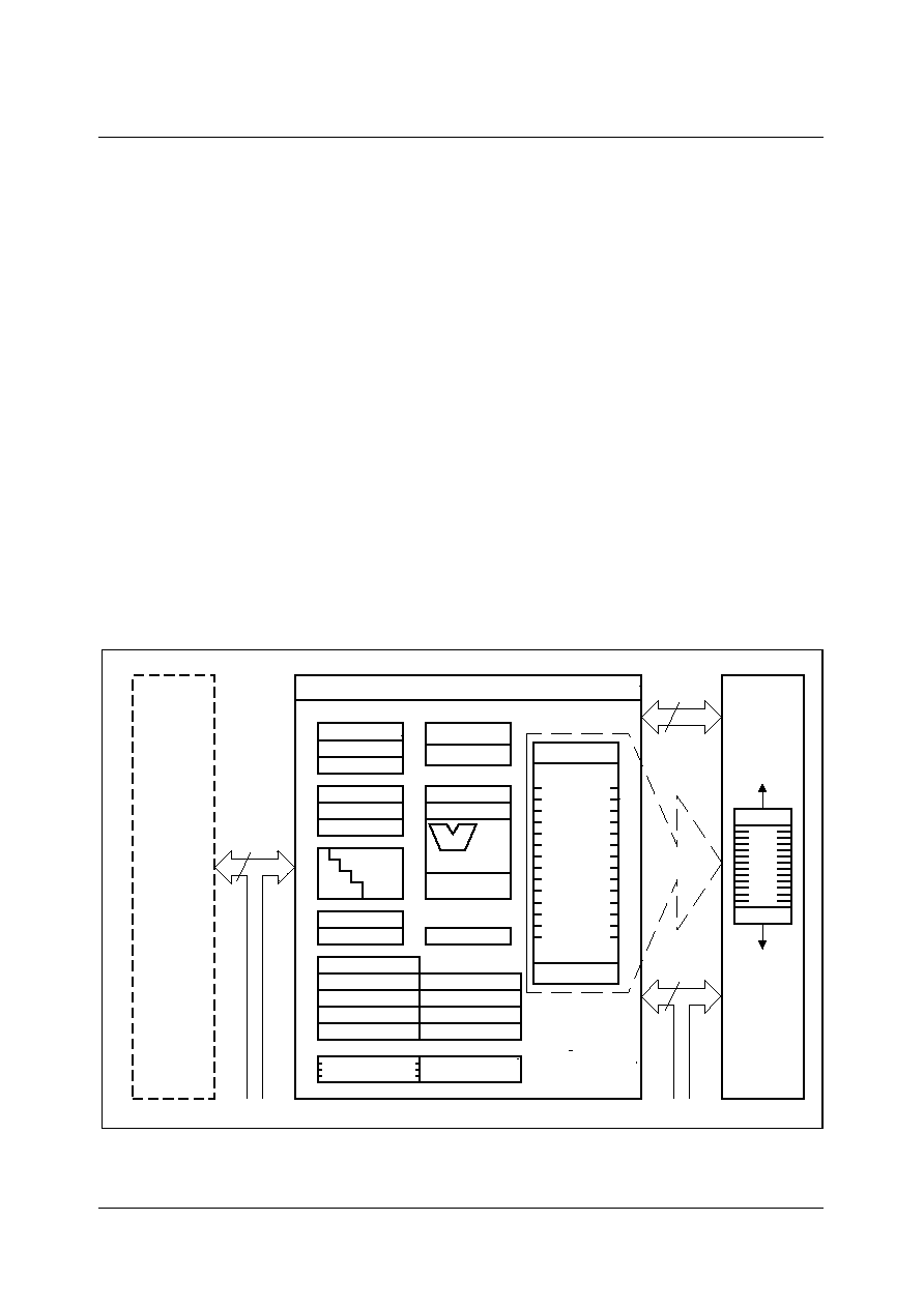
SDA 6000 / SDA 6001
PRELIMINARY DATA SHEET
Version 3.00
C16X Microcontroller
4 - 31
Micronas
4.6
Central Processing Unit
Basic tasks of the CPU are to fetch and decode instructions, to supply operands for the
arithmetic and logic unit (ALU), to perform operations on these operands in the ALU, and
to store the previously calculated results.
Since a four stage pipeline is implemented in M2, up to four instructions can be
processed in parallel. Most instructions of M2 are executed in one machine cycles
(2 CPU clock cycles) due to this parallelism. This chapter describes how the pipeline
works for sequential and branch instructions in general, and which hardware provisions
have been made, in particular, to speed up the execution of jump instructions. The
description of the general instruction timing includes standard and exceptional timing.
For instruction and operand fetches, the CPU is connected to the different areas
(external memory, program memory, internal dual-port RAM or (E)SFR area) either
internally or through the interfaces of the CPU (XBUS, program memory bus or
peripheral bus). Where the program memory bus and the peripheral bus are tightly
coupled to the CPU, XBUS accesses are performed, if possible, in parallel while the CPU
continues operating. If data is required but not yet available or if a new XBUS access is
requested by the CPU before a previous access has been completed, the CPU will be
held until the request can be satisfied.
Figure 4-10 CPU Block Diagram
MCB02147
CPU
SP
STKOV
STKUN
Instr. Reg.
Instr. Ptr.
Exec. Unit
4-Stage
Pipeline
MDH
MDL
PSW
SYSCON
Context Ptr.
Mul/Div-HW
R15
R0
General
Purpose
Registers
Bit-Mask Gen
Barrel - Shifter
ALU
(16-bit)
Data Page Ptr.
Code Seg. Ptr.
Internal
RAM
R15
R0
ROM
16
16
32
BUSCON 0
BUSCON 1
BUSCON 2
BUSCON 3
BUSCON 4
ADDRSEL 4
ADDRSEL 3
ADDRSEL 2
ADDRSEL 1

SDA 6000 / SDA 6001
PRELIMINARY DATA SHEET
Version 3.00
C16X Microcontroller
4 - 32
Micronas
Peripheral units are connected to the CPU by the peripheral bus or the XBUS and can
work practically independent of the CPU. Data and control information is interchanged
between the CPU and these peripherals by Special Function Registers (SFRs) or
external memory locations, depending on to which bus they are connected. Whenever
peripherals need a non-deterministic CPU action, the Interrupt Controller compares all
pending peripheral service requests with each other and prioritizes one of them. If the
priority of the current CPU operation is lower than the priority of the selected peripheral
request, an interrupt will occur.
Basically, there are two types of interrupt processing:
� Standard interrupt processing forces the CPU to save the current program status
and the return address to the stack before branching to the interrupt vector jump table.
� PEC interrupt processing steals just one machine cycle from the current CPU
activity to perform a single data transfer via the on-chip Peripheral Event Controller
(PEC).
System errors detected during program execution (so-called hardware traps) are also
processed as standard interrupts with a very high priority.
Besides its normal operation there are the following particular CPU states:
� Reset state: Any reset (hardware, software, watchdog) forces the CPU into a
predefined active state.
� IDLE state: The clock signal to the CPU itself is switched off, while the clocks for the
peripherals keep running.
� POWER DOWN state: All of the on-chip clocks are switched off.
A transition into an active CPU state is forced by an interrupt (if in IDLE mode) or by a
reset (if in POWER DOWN mode).
The IDLE, POWER DOWN and RESET states can be entered by particular system
control instructions.
A set of Special Function Registers is dedicated to the functions of the CPU core:
� General System Configuration:
SYSCON (RP0H)
� CPU Status Indication and Control: PSW
� Code Access Control:
IP, CSP
� Data Paging Control:
DPP0, DPP1, DPP2, DPP3
� GPRs Access Control:
CP
� System Stack Access Control:
SP, STKUN, STKOV
� Multiply and Divide Support:
MDL, MDH, MDC
� ALU Constants Support:
ZEROS, ONES
4.6.1
Instruction Pipelining
The instruction pipeline of the CPU separates instruction processing into four stages,
and each one has an individual task:

SDA 6000 / SDA 6001
PRELIMINARY DATA SHEET
Version 3.00
C16X Microcontroller
4 - 33
Micronas
1st �>FETCH:
In this stage the instruction selected by the Instruction Pointer (IP) and the Code
Segment Pointer (CSP) is fetched from either the program memory, internal RAM, or
external memory.
2nd �>DECODE:
In this stage the instructions are decoded and, if required, the operand addresses are
calculated and the respective operands are fetched. For all instructions, which implicitly
access the system stack, the SP register is either decremented or incremented, as
specified. For branch instructions the Instruction Pointer and the Code Segment Pointer
are updated to the desired branch target address (provided that the branch is taken).
3rd �>EXECUTE:
In this stage an operation is performed on the previously fetched operands in the ALU.
In addition, the condition flags in the PSW register are updated, as specified by the
instruction. All explicit writes to the SFR memory space and all auto-increment or auto-
decrement writes to GPRs used as indirect address pointers are also performed during
the execute stage of an instruction.
4th �>WRITE BACK:
In this stage all external operands and the remaining operands within the internal RAM
space are written back.
A particularity of the CPU are the so-called imported instructions. These imported
instructions are internally generated by the machine to provide the time needed to
process instructions which cannot be processed within one machine cycle. They are
automatically imported into the decoding stage of the pipeline, and then they pass
through the remaining stages like all standard instructions. Program interrupts are also
performed by means of imported instructions. Although these internally imported
instructions will not be noticed in reality, they are introduced here to ease the explanation
of the pipeline in the following:
Sequential Instruction Processing
Each single instruction has to pass through each of the four pipeline stages regardless
of whether all possible stage operations are performed or not. Since passing through one
pipeline stage takes at least one machine cycle, any isolated instruction takes at least
four machine cycles to be completed. Pipelining, however, allows parallel (i.e.
simultaneous) processing of up to four instructions. Thus, most of the instructions seem
to be processed during one machine cycle as soon as the pipeline has been filled once
after reset (see Figure 4-11).
SDA 6000 / SDA 6001
PRELIMINARY DATA SHEET
Version 3.00
C16X Microcontroller
4 - 34
Micronas
Instruction pipelining increases the average instruction throughput considered over a
certain period of time. In the following, any execution time specification of an instruction
always refers to the average execution time due to pipelined parallel instruction
processing.
Figure 4-11 Sequential Instruction Pipelining
Standard Branch Instruction Processing
Instruction pipelining helps to speed up sequential program processing. When a branch
is taken, the instruction which has been fetched in advance is usually not the instruction
which must be decoded next. Thus, at least one additional machine cycle is normally
required to fetch the branch target instruction. This extra machine cycle is provided by
means of an imported instruction (see Figure 4-12).
Figure 4-12 Standard Branch Instruction Pipelining
If a conditional branch is not taken, there is no deviation from the sequential program
flow, and thus no extra time is required. In this case, the instruction following the branch
instruction will enter the decoding stage of the pipeline at the beginning of the next
machine cycle after decoding the conditional branch instruction.
UED11124
1
I
I
2
I
3
I
4
I
5
I
6
1
I
2
I
1
I
3
I
2
I
1
I
3
I
2
I
I
4
4
I
3
I
I
5
FETCH
DECODE
EXECUTE
WRITEBACK
1 Machine Cycle
Time
UED11125
I
n+2
I
TARGET
FETCH
DECODE
EXECUTE
WRITEBACK
1 Machine Cycle
n
I
BRANCH
...
...
...
I
n
BRANCH
INJECT
I
(
)
BRANCH
n
I
TARGET+1
I
TARGET
I
I
(
)
INJECT
BRANCH
I
INJECT
TARGET
(
I
)
TARGET+1
I
TARGET+2
I
TARGET+2
TARGET+1
I
TARGET
I
I
TARGET+3
I
Injection
Time

SDA 6000 / SDA 6001
PRELIMINARY DATA SHEET
Version 3.00
C16X Microcontroller
4 - 35
Micronas
Cache Jump Instruction Processing
The CPU incorporates a jump cache to optimize conditional jumps, which are processed
repeatedly within a loop. Whenever a jump on cache is taken, the extra time to fetch the
branch target instruction can be saved, therefore causing the corresponding cache jump
instruction to need only one machine cycle.
This performance is achieved by the following mechanism:
Whenever a cache jump instruction passes through the decode stage of the pipeline for
the first time (and provided that the jump condition is met), the jump target instruction is
fetched as usual, causing a time delay of one machine cycle. In contrast to standard
branch instructions, however, the target instruction of a cache jump instruction (JMPA,
JMPR, JB, JBC, JNB, JNBS) is additionally stored in the cache after having been
fetched.
After repeatedly following each execution of the same cache jump instruction, the jump
target instruction is not fetched from program memory but taken from the cache and
immediately imported into the decoding stage of the pipeline (see Figure 4-13).
A time saving jump on cache is always taken after the second and any further occurrence
of the same cache jump instruction, unless an instruction, which has the fundamental
capability of changing the CSP register contents (JMPS, CALLS, RETS, TRAP, RETI),
or any standard interrupt has been processed during the period of time between two
following occurrences of the same cache jump instruction.
Figure 4-13 Cache Jump Instruction Pipelining
Particular Pipeline Effects
Since up to four different instructions are processed simultaneously, additional hardware
has been used in the CPU to consider all causal dependencies which may exist on
instructions in different pipeline stages without a loss of performance. This extra
hardware (i.e. for "forwarding" operand read and write values) resolves most of the
UED11126
I
n+2
I
TARGET
FETCH
DECODE
EXECUTE
WRITEBACK
1 Machine Cycle
1st Loop Iteration
...
I
n
Cache Jmp
INJECT
I
(
)
TARGET+1
I
TARGET+2
I
Injection
Cache Jmp
I
n
I
INJECT
TARGET
(
I
)
TARGET+1
I
Cache Jmp
Cache Jmp
I
...
n
I
n+2
TARGET+1
TARGET
I
I
Cache Jmp
I
n
TARGET
I
Cache Jmp
Repeated Loop Iteration
Target Instruction
Injection of Cached

SDA 6000 / SDA 6001
PRELIMINARY DATA SHEET
Version 3.00
C16X Microcontroller
4 - 36
Micronas
possible conflicts (e.g. multiple usage of buses) in a time optimized way and thus usually
avoids the pipeline being noticed by the user. However, there are some very rare cases,
where the CPU, being a pipelined machine, requires attention by the programmer. In
these cases the delays caused by pipeline conflicts can be used for other instructions in
order to optimize performance.
Context Pointer Updating
An instruction which calculates a physical GPR operand address via the CP register, is
mostly not capable of using a new CP value, which is to be updated by an immediately
preceding instruction. Thus, to make sure that the new CP value is used, at least one
instruction must be inserted between a CP-changing and a subsequent GPR-using
instruction, as shown in the following example:
I
n
: SCXT CP, #0FC00h
; select a new context
I
n+1
:
...
.
; must not be an instruction using a GPR
I
n+2
: MOV R0, #dataX
; write to GPR 0 in the new context
Data Page Pointer Updating
An instruction, which calculates a physical operand address via a particular DPPn (n = 0
to 3) register, is mostly not capable of using a new DPPn register value, which is to be
updated by an immediately preceding instruction. Thus, to make sure that the new DPPn
register value is used, at least one instruction must be inserted between a DPPn-
changing instruction and a subsequent instruction which implicitly uses DPPn via a long
or indirect addressing mode, as shown in the following example:
I
n
: MOV DPP0, #4
; select data page 4 via DPP0
I
n+1
:
...
.
; must not be an instruction using DPP0
I
n+2
: MOV DPP0:0000H, R1; move contents of R1 to address location
01'0000
H
; (in data page 4) supposed segmentation
is enabled
Explicit Stack Pointer Updating
None of the RET, RETI, RETS, RETP or POP instructions are capable of correctly using
a new SP register value, which is to be updated by an immediately preceding instruction.
Thus, in order to use the new SP register value without erroneously performed stack
accesses, at least one instruction must be inserted between an explicitly SP-writing and
any subsequent just mentioned implicitly SP-using instructions, as shown in the following
example:
I
n
: MOV SP, #0FA40H; select a new top of stack
I
n+1
:
...
.
; must not be an instruction popping
operands
; from the system stack

SDA 6000 / SDA 6001
PRELIMINARY DATA SHEET
Version 3.00
C16X Microcontroller
4 - 37
Micronas
I
n+2
: POP R0
; pop word value from new top of stack into
R0
Note: Conflicts with instructions writing to the stack (PUSH, CALL, SCXT) are solved
internally by the CPU logic.
Controlling Interrupts
Software modifications (implicit or explicit) of the PSW are done in the execute phase of
the respective instructions. In order to maintain fast interrupt responses, however, the
current interrupt prioritization round does not consider these changes, i.e. an interrupt
request may be acknowledged after the instruction that disables interrupts via IEN or
ILVL or after the subsequent instructions. Timecritical instruction sequences therefore
should not begin directly after the instruction disabling interrupts, as shown in the
following example:
INT_OFF:
BCLR IEN
; globally disable interrupts
I
N-1
; non-critical instruction
CRIT_1ST: I
N
; begin of uninterruptable critical sequence
...
CRIT_LAST:I
N+x
; end of uninterruptable critical sequence
INT_ON:
BSET IEN
; globally re-enable interrupts
Note: The described delay of 1 instruction also applies for enabling the interrupts system
i.e. no interrupt requests are acknowledged until the instruction after the enabling
instruction.
Changing the System Configuration
The instruction following an instruction that changes the system configuration via register
SYSCON (e.g. the mapping of the program memory, segmentation, stack size) cannot
use the new resources (e.g. program memory or stack). In these cases an instruction
that does not access these resources should be inserted. Code accesses to the new
program memory area are only possible after an absolute branch to this area.
Note: As a rule, instructions that change program memory mapping should be executed
from internal RAM or external / XBUS memory.
BUSCON/ADDRSEL and XBCON/XADRS
The instruction following an instruction that changes the properties of an external / XBUS
address area cannot access operands within the new area. In these cases an instruction
that does not access this address area should be inserted. Code accesses to the new
address area should be made after an absolute branch to this area.
Note: As a rule, instructions that change external bus properties should not be executed
from the respective external memory area.

SDA 6000 / SDA 6001
PRELIMINARY DATA SHEET
Version 3.00
C16X Microcontroller
4 - 38
Micronas
Timing
Instruction pipelining reduces the average instruction processing time on a wide scale
(usually from four to one machine cycles). However, there are some rare cases where a
particular pipeline situation causes the processing time for a single instruction to be
extended either by a half or by one machine cycle. Although this additional time
represents only a tiny part of the total program execution time, it might be of interest to
avoid these pipeline-caused time delays in time critical program modules.
Besides a general execution time description, the following section provides some hints
on how to optimize time-critical program parts with regard to such pipeline-caused timing
particularities.
4.6.2
Bit-Handling and Bit-Protection
The CPU provides several mechanisms to manipulate bits. These mechanisms either
manipulate software flags within the internal RAM, control on-chip peripherals via control
bits in their respective SFRs or control IO functions via port pins.
The instructions BSET, BCLR, BAND, BOR, BXOR, BMOV, BMOVN explicitly set or
clear specific bits. The instructions BFLDL and BFLDH allow the manipulation of up to
8 bits of a specific byte at one time. The instructions JBC and JNBS implicitly clear or set
the specified bit when the jump is taken. The instructions JB and JNB (also conditional
jump instructions that refer to flags) evaluate the specified bit to determine if the jump is
to be taken.
Note: Bit operations on undefined bit locations will always read a bit value of `0', while
the write access will not effect the respective bit location.
All instructions that manipulate single bits or bit groups internally use a read-modify-write
sequence that accesses the whole word, which contains the specified bit(s).
This method has several consequences:
� Bits can only be modified within the internal address areas, i.e. internal RAM and
SFRs. External locations cannot be used with bit instructions.
The upper 256 bytes of the SFR area, the ESFR area and the internal RAM are bit-
addressable (see Chapter 4.2), i.e. those register bits located within the respective
sections can be directly manipulated using bit instructions. The other SFRs must be byte/
word accessed.
Note: All GPRs are bit-addressable independent of the allocation of the register bank via
the context pointer CP. Even GPRs which are allocated to not bit-addressable
RAM locations provide this feature.
� The read-modify-write approach may be critical with hardware-effected bits. In these
cases the hardware may change specific bits while the read-modify-write operation is
in progress, where the writeback would overwrite the new bit value generated by the
hardware. The solution is either the implemented hardware protection (see below) or
SDA 6000 / SDA 6001
PRELIMINARY DATA SHEET
Version 3.00
C16X Microcontroller
4 - 39
Micronas
realization through special programming (see "Particular Pipeline Effects" on
page 35).
Protected bits are not changed during the read-modify-write sequence, i.e. when
hardware sets e.g. an interrupt request flag between the read and the write of the read-
modify-write sequence. The hardware protection logic guarantees that only the intended
bit(s) is/are effected by the write-back operation.
Note: If a conflict occurs between a bit manipulation generated by hardware and an
intended software access the software access has priority and determines the
final value of the respective bit.
4.6.3
Instruction State Times
Basically, the time needed to execute an instruction depends on where the instruction is
fetched from, and where possible operands are read from or written to. The fastest
processing mode of M2 is the execution of a program fetched from the program memory.
In this case most of the instructions can be processed within just one machine cycle,
which is also the general minimum execution time.
This section summarizes the execution times in a very condensed way. A detailed
description of the execution times for the various instructions and the specific exceptions
can be found in the "C16x Family Instruction Set Manual".
The table below shows the minimum execution times required to process an M2
instruction fetched from the program memory, the internal RAM or from external / XBUS
memory. These execution times apply to most of the M2 instructions - except some of
the branches, the multiplication, the division and a special move instruction. In case of
program execution from the program memory there is no execution time dependency on
the instruction length except for some special branch situations. The numbers in the
table are in units of CPU clock cycles and assume no wait-states.
Execution from the internal RAM provides flexibility in terms of loadable and modifiable
code on the account of execution time.
Table 4-2
Minimum Execution Times
Instruction Fetch
Word Operand Access
Memory Area
Word
Instruction
Doubleword
Instruction
Read from
Write to
Internal code memory
2
2
2
�
Internal RAM
6
8
0/1
0
16-bit Demux Bus
2
4
2
2
16-bit Mux Bus
3
6
3
3

SDA 6000 / SDA 6001
PRELIMINARY DATA SHEET
Version 3.00
C16X Microcontroller
4 - 40
Micronas
Execution from external memory strongly depends on the selected bus mode and the
programming of the bus cycles (wait-states).
The operand and instruction accesses listed below can extend the execution time of an
instruction:
� Internal code memory operand reads (same for byte and word operand reads)
� Internal RAM operand reads via indirect addressing modes
� Internal SFR operand reads immediately after writing
� External operand reads
� External operand writes
� Jumps to non-aligned double word instructions in the program memory space
� Testing Branch Conditions immediately after PSW writes
4.6.4
CPU Special Function Registers
The CPU requires a set of Special Function Registers (SFRs) to maintain the system
state information, to supply the ALU with register-addressable constants and to control
system and bus configuration, multiply and divide ALU operations, code memory
segmentation, data memory paging, and accesses to the General Purpose Registers
and the System Stack.
The access mechanism for these SFRs in the CPU core is identical to the access
mechanism for any other SFR. Since all SFRs can simply be controlled by means of any
instruction, which is capable of addressing the SFR memory space, a lot of flexibility has
been gained, without the need to create a set of system-specific instructions.
Note, however, that there are user access restrictions for some of the CPU core SFRs
to ensure proper processor operations. The instruction pointer IP and code segment
pointer CSP cannot be accessed directly. They can only be changed indirectly via
branch instructions.
The PSW, SP, and MDC registers can not only be modified explicitly by the programmer,
but also implicitly by the CPU during normal instruction processing. Note that any explicit
write request (via software) to an SFR supersedes a simultaneous modification by
hardware of the same register.
Note: Any write operation to a single byte of an SFR clears the non-addressed
complementary byte within the specified SFR.
Non-implemented (reserved) SFR bits cannot be modified, and will always supply
a read value of '0'.
System Configuration Register SYSCON
This bit-addressable register provides general system configuration and control
functions. The reset value for register SYSCON depends on the state of the PORT4 pins
during reset.

SDA 6000 / SDA 6001
PRELIMINARY DATA SHEET
Version 3.00
C16X Microcontroller
4 - 41
Micronas
SYSCON
Reset Value: 0400
H
Bit
Function
XPEN
XBUS Peripheral Enable Bit
`0': Accesses to the on-chip X-Peripherals and their functions are
disabled.
`1': The
on-chip
X-Peripherals
are enabled and can be accessed.
RSOEN
Reset Output Enable Bit
`0': The contrast reduction signal is driven on pin 104.
`1': The reset output signal is driven on pin 104, i.e. pin 104 is pulled
low during internal reset sequence.
Note: Refer also to Chapter 6.7
CSCFG
Select Line Configuration Control
`0': Latched select line mode for X-Peripherals.
`1': Select lines for access cycles via XBUS are directly derived from
the address lines.
Note: CSCFG = `1' is recommended. The effect of the switch is not
visible at an external interface.
ROMEN
PM-Bus Enable Bit
`0': PM-Bus disabled: accesses to the ROM area use the XBUS.
`1': PM-Bus enabled: PM-Bus enabled for access cycles to the ROM
area.
Note: The recommended value ROMEN = `1' is set by hardware during
reset.
SGTDIS
Segmentation Disable/Enable Control
`0': Segmentation
enabled (CSP is saved/restored during interrupt
entry/exit).
`1': Segmentation
disabled
(Only IP is saved/restored).
5
4
3
2
1
0
11
10
9
8
7
6
15
14
13
12
rw
rw
rw
rw
rw
rw
STKSZ(2..0)
ROM
S1
SGT
DIS
ROM
EN
-
-
-
CS
CFG
-
-
RSO
EN
XPEN
-
-
rw

SDA 6000 / SDA 6001
PRELIMINARY DATA SHEET
Version 3.00
C16X Microcontroller
4 - 42
Micronas
Note: Register SYSCON cannot be changed after execution of the EINIT instruction.
Segmentation Disable/Enable Control (SGTDIS)
Bit SGTDIS allows to select either the segmented or non-segmented memory mode.
In non-segmented memory mode (SGTDIS = `1') it is assumed that the code address
space is restricted to 64 KBytes (segment 0) and thus 16 bits are sufficient to represent
all code addresses. For implicit stack operations (CALL or RET) the CSP register is
totally ignored and only the IP is saved to and restored from the stack.
In segmented memory mode (SGTDIS = `0') it is assumed that the whole address space
is available for instructions. For implicit stack operations (CALL or RET) the CSP register
and the IP are saved to and restored from the stack. After reset the segmented memory
mode is selected.
Note: Bit SGTDIS controls if the CSP register is pushed onto the system stack in addition
to the IP register before an interrupt service routine is entered, and it is repopped
when the interrupt service routine is left again.
System Stack Size (STKSZ)
This bitfield defines the size of the physical system stack, which is located in the internal
RAM of M2. An area of 32 ... 512 words or all of the internal RAM may be dedicated to
the system stack. A so-called "circular stack" mechanism allows the use of a bigger
virtual stack than this dedicated RAM area.
The Processor Status Word PSW
This bit-addressable register reflects the current state of the microcontroller. Two groups
of bits represent the current ALU status, and the current CPU interrupt status. A separate
bit (USR0) within register PSW is provided as a general purpose user flag.
ROMS1
Internal ROM Mapping
`0':
External ROM area mapped to segment 0
(00'0000
H
... 00'7FFF
H
)
`1': External ROM area mapped to segment 1
(01'0000
H
... 01'7FFF
H
).
Note: ROMS1 = `0' is recommended.
STKSZ
(2 ... 0)
System Stack Size
Selects the size of the system stack (in the internal RAM) from 32 to
1024 words.
Bit
Function

SDA 6000 / SDA 6001
PRELIMINARY DATA SHEET
Version 3.00
C16X Microcontroller
4 - 43
Micronas
PSW
Reset Value: 0000
H
ALU Status (N, C, V, Z, E, MULIP)
The condition flags (N, C, V, Z, E) within the PSW indicate the ALU status after the last
recently performed ALU operation. They are set by most of the instructions due to
specific rules, which depend on the ALU or data movement operation performed by an
instruction.
After execution of an instruction which explicitly updates the PSW register, the condition
flags cannot be interpreted as described in the following, because any explicit write to
the PSW register supersedes the condition flag values, which are implicitly generated by
the CPU. Explicitly reading the PSW register provides a read value that represents the
state of the PSW register after execution of the immediately preceding instruction.
Note: After reset, all of the ALU status bits are cleared.
Bit
Function
N
Negative Result
Set, when the result of an ALU operation is negative.
C
Carry Flag
Set, when the result of an ALU operation produces a carry bit.
V
Overflow Result
Set, when the result of an ALU operation produces an overflow.
Z
Zero Flag
Set, when the result of an ALU operation is zero.
E
End of Table Flag
Set, when the source operand of an instruction is 8000
H
or 80
H
.
MULIP
Multiplication/Division In Progress
`0':
There is no multiplication/division in progress.
`1': A
multiplication/division has been interrupted.
USR0
User General Purpose Flag
May be used by the application software.
HLDEN,
ILVL, IEN
Interrupt and EBC Control Fields
Define the response to interrupt requests and enable external bus
arbitration.
5
4
3
2
1
0
11
10
9
8
7
6
15
14
13
12
rw
rw
rw
rw
rw
rw
rw
rw
rw
ILVL(3..0)
IEN
HLD
EN
-
-
-
USR0
MUL
IP
E
Z
V
C
N
rw

SDA 6000 / SDA 6001
PRELIMINARY DATA SHEET
Version 3.00
C16X Microcontroller
4 - 44
Micronas
� N-Flag: For most of the ALU operations, the N-flag is set to `1' if the most significant
bit of the result contains a `1', otherwise it is cleared. In the case of integer operations
the N-flag can be interpreted as the sign bit of the result (negative: N = `1', positive:
N = `0'). Negative numbers are always represented as the 2's complement of the
corresponding positive number. The range of signed numbers extends from `�8000
H
'
to `+7FFF
H
' for the word data type, or from `�80
H
' to `+7F
H
' for the byte data type. For
Boolean bit operations with only one operand, the N-flag represents the previous state
of the specified bit. For Boolean bit operations with two operands, the N-flag
represents the logical XORing of the two specified bits.
� C-Flag: After an addition, the C-flag indicates that a carry from the most significant bit
of the specified word or byte data type has been generated. After a subtraction or a
comparison, the C-flag indicates a borrow, which represents the logical negation of a
carry for the addition.
This means that the C-flag is set to `1' if no carry from the most significant bit of the
specified word or byte data type has been generated during a subtraction, which is
performed internally by the ALU as a 2's complement addition, and the C-flag is
cleared when this complement addition causes a carry.
The C-flag is always cleared for logical, multiply and divide ALU operations, because
these operations cannot cause a carry.
For shift and rotate operations the C-flag represents the value of the bit last shifted
out. If a shift count of zero is specified, the C-flag will be cleared. The C-flag is also
cleared for a prioritized ALU operation because a `1' is never shifted out of the MSB
during the normalization of an operand.
For Boolean bit operations with only one operand the C-flag is always cleared. For
Boolean bit operations with two operands the C-flag represents the logical ANDing of
the two specified bits.
� V-Flag: For addition, subtraction and 2's complementation the V-flag is always set to
`1', if the result overflows the maximum range of signed numbers, which are
representable by either 16 bits for word operations (`�8000
H
' to `+7FFF
H
'), or by 8 bits
for byte operations (`�80
H
' to `+7F
H
'), otherwise the V-flag is cleared. Note that the
result of an integer addition, integer subtraction, or 2's complement is not valid if the
V-flag indicates an arithmetic overflow.
For multiplication and division the V-flag is set to `1' if the result cannot be represented
in a word data type, otherwise it is cleared. Note that a division by zero will always
cause an overflow. In contrast to the result of a division, the result of a multiplication
is valid regardless of whether the V-flag is set to `1' or not.
Since logical ALU operations cannot produce an invalid result, the V-flag is cleared by
these operations.
The V-flag is also used as a "Sticky Bit" for rotate right and shift right operations. By
only using the C-flag, a rounding error caused by a shift right operation can be
estimated up to a quantity of one half of the LSB of the result. In conjunction with the

SDA 6000 / SDA 6001
PRELIMINARY DATA SHEET
Version 3.00
C16X Microcontroller
4 - 45
Micronas
V-flag, the C-flag allows the evaluation of the rounding error with a finer resolution
(see Table 4-3).
For Boolean bit operations with only one operand the V-flag is always cleared. For
Boolean bit operations with two operands the V-flag represents the logical ORing of
the two specified bits.
� Z-Flag: The Z-flag is normally set to `1' if the result of an ALU operation equals zero,
otherwise it is cleared.
For the addition and subtraction with carry, the Z-flag is only set to `1' if the Z-flag
already contains a `1' and the result of the current ALU operation additionally equals
zero. This mechanism is provided for the support of multiple precision calculations.
For Boolean bit operations with only one operand the Z-flag represents the logical
negation of the previous state of the specified bit. For Boolean bit operations with two
operands the Z-flag represents the logical NORing of the two specified bits. For the
prioritized ALU operation the Z-flag indicates whether the second operand is zero or
not.
� E-Flag: The E-flag can be altered by instructions, which perform ALU or data
movement operations. The E-flag is cleared by those instructions which cannot be
reasonably used for table search operations. In all other cases the E-flag is set
depending on the value of the source operand to signify whether the end of a search
table is reached or not. If the value of the source operand of an instruction equals the
lowest negative number, which is representable by the data format of the
corresponding instruction (`8000
H
' for the word data type, or `80
H
' for the byte data
type), the E-flag is set to `1', otherwise it is cleared.
� MULIP-Flag: The MULIP-flag will be set to `1' by hardware upon entry to an interrupt
service routine, when a multiply or divide ALU operation was interrupted before
completion. Depending on the state of the MULIP bit, the hardware decides whether
multiplication or division must be continued or not after the end of an interrupt service.
The MULIP bit is overwritten with the contents of the stacked MULIP-flag when the
return-from-interrupt-instruction (RETI) is executed. This normally means that the
MULIP-flag is cleared again after that.
Note: The MULIP flag is a part of the task environment. When the interrupting service
routine does not return to the interrupted multiply/divide instruction (i.e. as in the
Table 4-3
Shift Right Rounding Error Evaluation
C-Flag
V-Flag
Rounding Error Quantity
0
0
1
1
0
1
0
1
-
No rounding error
-
0 < Rounding error
<
1
/
2
LSB
Rounding error
=
1
/
2
LSB
Rounding error
>
1
/
2
LSB

SDA 6000 / SDA 6001
PRELIMINARY DATA SHEET
Version 3.00
C16X Microcontroller
4 - 46
Micronas
case of a task scheduler that switches between independent tasks), the MULIP
flag must be saved as part of the task environment and must be updated
accordingly for the new task before this task is entered.
CPU Interrupt Status (IEN, ILVL)
The Interrupt Enable bit allows for global enabling (IEN = `1') or disabling (IEN = `0') of
interrupts. The four-bit Interrupt Level field (ILVL) specifies the priority of the current CPU
activity. The interrupt level is updated by hardware upon entry into an interrupt service
routine, but it can also be modified via software to prevent other interrupts from being
acknowledged. In case an interrupt level `15' has been assigned to the CPU, it has the
highest possible priority, and thus the current CPU operation cannot be interrupted
except by hardware traps or external non-maskable interrupts. For details please refer
to Chapter 5.
After reset all interrupts are globally disabled, and the lowest priority (ILVL = 0) is
assigned to the initial CPU activity.
The Instruction Pointer IP
This register determines the 16-bit intra-segment address of the currently fetched
instruction within the code segment selected by the CSP register. The IP register is not
mapped into the M2's address space, and thus it is not directly accessible by the
programmer. The IP can, however, be modified indirectly via the stack by means of a
return instruction.
The IP register is implicitly updated by the CPU for branch instructions and after
instruction fetch operations.
IP
Reset Value: 0000
H
The Code Segment Pointer CSP
This non-bit addressable register selects the code segment being used at run-time to
access instructions. The lower 8 bits of register CSP select one of up to 256 segments
of 64 KBytes each, while the upper 8 bits are reserved for future use.
Bit
Function
ip(15 ... 0)
Specifies the intra segment offset, from where the current instruction is
to be fetched. IP refers to the current segment <SEGNR>.
5
4
3
2
1
0
11
10
9
8
7
6
15
14
13
12
r/w
ip (15..0)

SDA 6000 / SDA 6001
PRELIMINARY DATA SHEET
Version 3.00
C16X Microcontroller
4 - 47
Micronas
CSP
Reset Value: 0000
H
Code memory addresses are generated by directly extending the 16-bit contents of the
IP register by the contents of the CSP register, as shown in Figure 4-14.
In case of the segmented memory mode the selected number of segment address bits
(via bit field SALSEL) of the CSP register is output on the respective segment address
pins of Port 4 for all external code accesses. For non-segmented memory mode the
content of this register is not significant, because all code accesses are automatically
restricted to segment 0.
Note: The CSP register can only be read but not written by data operations. It is,
however, modified either directly by means of the JMPS and CALLS instructions,
or indirectly via the stack by means of the RETS and RETI instructions.
Upon the acceptance of an interrupt or the execution of a software TRAP
instruction, the CSP register is automatically set to zero.
Bit
Function
SEGNR
(7 ... 0)
Segment Number
Specifies the code segment, from where the current instruction is to be
fetched. SEGNR is ignored when segmentation is disabled.
-
-
-
-
-
5
4
3
2
1
0
11
10
9
8
7
6
15
14
13
12
-
-
-
r
-
-
-
-
-
-
-
-
SEGNR(7..0)
SDA 6000 / SDA 6001
PRELIMINARY DATA SHEET
Version 3.00
C16X Microcontroller
4 - 48
Micronas
Figure 4-14 Addressing via the Code Segment Pointer
Note: When segmentation is disabled, the IP value is used directly as the 16-bit address.
The Data Page Pointers DPP0, DPP1, DPP2, DPP3
These four non-bit addressable registers select up to four different data pages being
active simultaneously at run-time. The lower 10 bits of each DPP register select one of
the 1024 possible 16-Kbyte data pages while the upper 6 bits are reserved for future use.
The DPP registers allow access to the entire memory space in pages of 16 Kbytes each.
DPP0
Reset Value: 0000
H
DPP1
Reset Value: 0001
H
MCA02265
255
1
15
0
IP Register
254
0
Code Segment
FF'FFFF H
FE'0000H
01'0000H
00'0000H
CSP Register
15
0
24/20/18-Bit Physical Code Address
-
-
-
5
4
3
2
1
0
11
10
9
8
7
6
15
14
13
12
-
rw
-
-
-
-
-
-
-
-
DPP0PN
-
-
-
5
4
3
2
1
0
11
10
9
8
7
6
15
14
13
12
-
rw
-
-
-
-
-
-
-
-
DPP1PN
SDA 6000 / SDA 6001
PRELIMINARY DATA SHEET
Version 3.00
C16X Microcontroller
4 - 49
Micronas
DPP2
Reset Value: 0002
H
DPP3
Reset Value: 0003
H
The DPP registers are implicitly used whenever data accesses to any memory location
are made via indirect or direct long 16-bit addressing modes (except for override
accesses via EXTended instructions and PEC data transfers). After reset, the Data Page
Pointers are initialized in a way that all indirect or direct long 16-bit addresses result in
identical 18-bit addresses. This allows access to data pages 3 ... 0 within segment 0 as
shown in the figure below. If the user does not want to use any data paging, no further
action is required.
Data paging is performed by concatenating the lower 14 bits of an indirect or direct long
16-bit address with the contents of the DPP register selected by the upper two bits of the
16-bit address. The contents of the selected DPP register specify one of the 1024
possible data pages. This data page base address, together with the 14-bit page offset,
forms the physical 24-bit address (selectable part is driven to the address pins).
In case of non-segmented memory mode, only the two least significant bits of the
implicitly selected DPP register are used to generate the physical address. Thus,
extreme care should be taken when changing the content of a DPP register if a non-
segmented memory model is selected, because otherwise unexpected results could
occur.
In case of the segmented memory mode the selected number of segment address bits
(via bit field SALSEL) of the respective DPP register is output on the respective segment
address pins of Port 4 for all external data accesses.
A DPP register can be updated via any instruction, which is capable of modifying an
SFR.
Bit
Function
DPPxPN
Data Page Number of DPPx
Specifies the data page selected via DPPx. Only the least significant two
bits of DPPx are significant, when segmentation is disabled.
-
-
-
5
4
3
2
1
0
11
10
9
8
7
6
15
14
13
12
-
rw
-
-
-
-
-
-
-
-
DPP2PN
-
-
-
5
4
3
2
1
0
11
10
9
8
7
6
15
14
13
12
-
rw
-
-
-
-
-
-
-
-
DPP3PN
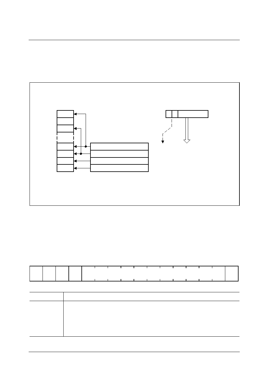
SDA 6000 / SDA 6001
PRELIMINARY DATA SHEET
Version 3.00
C16X Microcontroller
4 - 50
Micronas
Note: Due to the internal instruction pipeline, a new DPP value is not yet usable for the
operand address calculation of the instruction immediately following the updating
of the DPP register by the instruction.
Figure 4-15 Addressing via the Data Page Pointers
The Context Pointer CP
This non-bit addressable register is used to select the current register context. This
means that the CP register value determines the address of the first General Purpose
Register (GPR) within the current register bank of up to 16 word and/or byte GPRs.
CP
Reset Value: FC00
H
Bit
Function
cp
Modifiable Portion of Register CP
Specifies the (word) base address of the current register bank.
When writing a value to register CP with bits CP.11 ... CP.9 = `000', bits
CP.11 ... CP.10 are set to `11' by hardware, in all other cases all bits of
bit field "cp" receive the written value.
MCA02264
1023
1022
1021
3
2
1
0
DPP Registers
DPP3-11
DPP2-10
DPP1-01
DPP0-00
15 14
0
16-Bit Data Address
14-Bit
Intra-Page Address
(concatenated with
content of DPPx).
Affer reset or with segmentation disabled the DPP registers select data pages 3...0.
All of the internal memory is accessible in these cases.
1
0
1
5
4
3
2
1
0
11
10
9
8
7
6
15
14
13
12
r
rw
r
r
r
1
1
r
cp
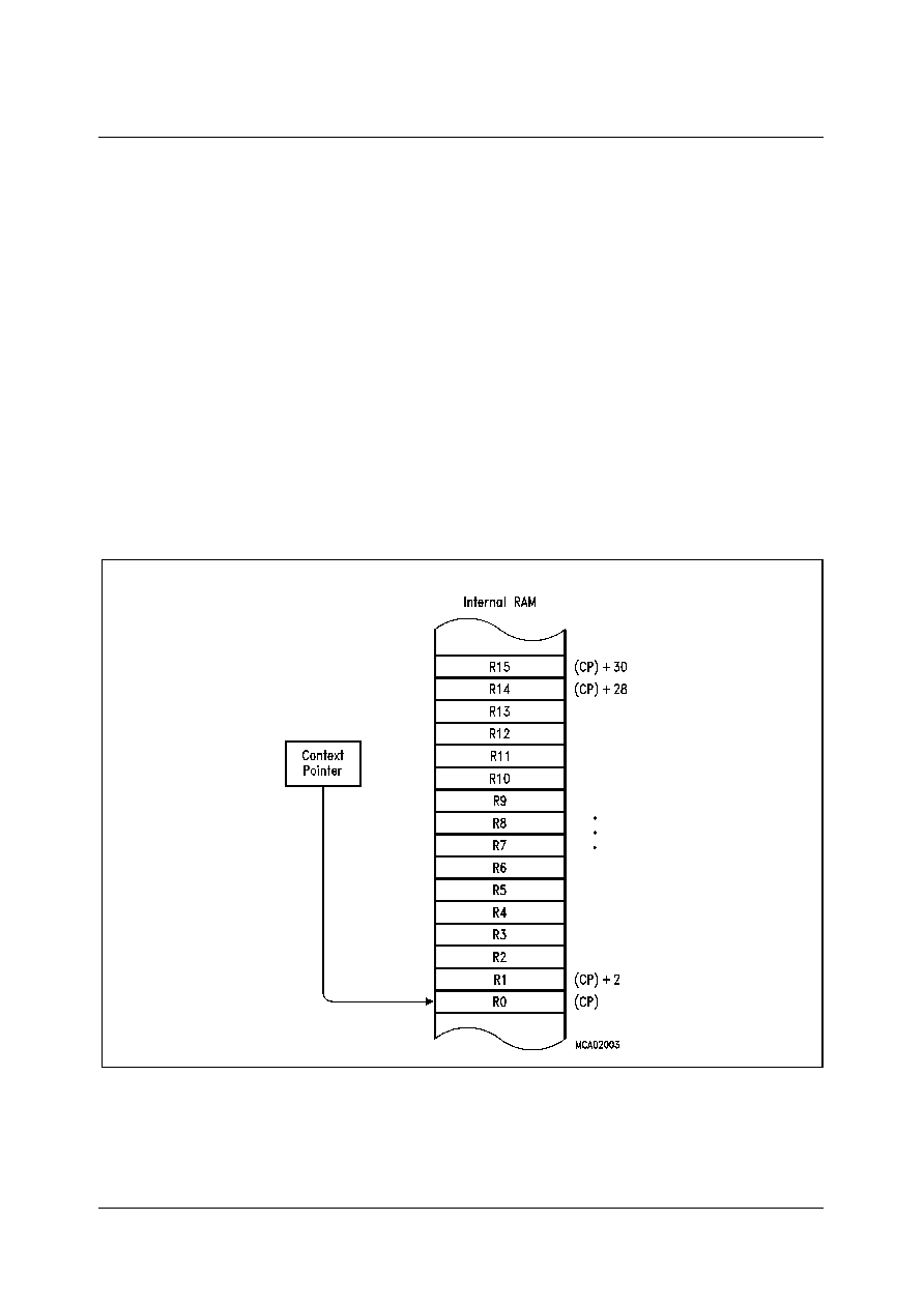
SDA 6000 / SDA 6001
PRELIMINARY DATA SHEET
Version 3.00
C16X Microcontroller
4 - 51
Micronas
Note: It is the user's responsibility that the physical GPR address specified via CP
register plus short GPR address must always be an internal RAM location. If this
condition is not met, unexpected results may occur.
� Do not set CP below the IRAM start address, i.e. 00'FA00
H
/00'F600
H
/00'F200
H
(1/2/3KB)
� Do not set CP above 00'FDFE
H
� Be careful when using the upper GPRs with CP above 00'FDE0
H
The CP register can be updated via any instruction which is capable of modifying an
SFR.
Note: Due to the internal instruction pipeline, a new CP value is not yet usable for GPR
address calculations of the instruction immediately following the instruction
updating the CP register.
The Switch Context instruction (SCXT) allows the saving of the contents of the CP
register onto the stack and updating of it with a new value in just one machine cycle.
Figure 4-16 Register Bank Selection via Register CP
Several addressing modes use the CP register implicitly for address calculations. The
addressing modes mentioned below are described in the "C16x Family Instruction Set
Manual".

SDA 6000 / SDA 6001
PRELIMINARY DATA SHEET
Version 3.00
C16X Microcontroller
4 - 52
Micronas
Short 4-Bit GPR Addresses (mnemonic: Rw or Rb) specify an address relative to the
memory location specified by the contents of the CP register, i.e. the base of the current
register bank.
Depending on whether a relative word (Rw) or byte (Rb) GPR address is specified, the
short 4-bit GPR address is sometimes multiplied by two before it is added to the contents
of the CP register (see Figure 4-17). Thus, in this way, both byte and word GPR
accesses are possible.
GPRs used as indirect address pointers are always word accessed. For some
instructions only the first four GPRs can be used as indirect address pointers. These
GPRs are specified by short 2-bit GPR addresses. The respective physical address
calculation is identical to that for the short 4-bit GPR addresses.
Short 8-Bit Register Addresses (mnemonic: reg or bitoff), within a range from F0
H
to
FF
H
, interpret the four least significant bits as short 4-bit GPR addresses, while the four
most significant bits are ignored. The respective physical GPR address calculation is
identical to that for the short 4-bit GPR addresses. For single bit accesses on a GPR, the
GPR's word address is calculated as described above, but the position of the bit within
the word is specified by a separate additional 4-bit value.
Figure 4-17 Implicit CP Use by Short GPR Addressing Modes
The Stack Pointer SP
This non-bit addressable register is used to point to the top of the internal system stack
(TOS). The SP register is pre-decremented whenever data is to be pushed onto the
stack, and it is post-incremented whenever data is to be popped from the stack. Thus,
the system stack grows from higher to lower memory locations.
Since the least significant bit of the SP register is tied to `0', and bits 15 through 12 are
tied to `1' by hardware, the SP register can only contain values from F000
H
to FFFE
H
.
This allows access to a physical stack within the internal RAM of the M2. A virtual stack
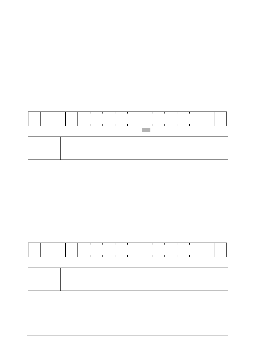
SDA 6000 / SDA 6001
PRELIMINARY DATA SHEET
Version 3.00
C16X Microcontroller
4 - 53
Micronas
(usually bigger) can be realized via software. This mechanism is supported by the
STKOV and STKUN registers (see respective descriptions below).
The SP register can be updated via any instruction, which is capable of modifying an
SFR.
Note: Due to the internal instruction pipeline, a POP or RETURN instruction must not
immediately follow an instruction updating the SP register.
SP
Reset Value: FC00
H
The Stack Overflow Pointer STKOV
This non-bit addressable register is compared against the SP register after each
operation, which pushes data onto the system stack (e.g. PUSH and CALL instructions
or interrupts) and after each subtraction from the SP register. If the contents of the SP
register are less than the content of the STKOV register, a stack overflow hardware trap
will occur.
Since the least significant bit of register STKOV is tied to `0' and bits 15 through 12 are
tied to `1' by hardware, the STKOV register can only contain values from F000
H
to
FFFE
H
.
STKOV
Reset Value: FA00
H
The Stack Overflow Trap (entered when (SP) < (STKOV)) may be used in two different
ways:
� Fatal error indication treats the stack overflow as a system error through the
associated trap service routine. Under these circumstances data in the bottom of the
Bit
Function
sp
Modifiable portion of register SP
Specifies the top of the internal system stack.
Bit
Function
stkov
Modifiable portion of register STKOV
Specifies the lower limit of the internal system stack.
1
0
1
5
4
3
2
1
0
11
10
9
8
7
6
15
14
13
12
r
rw
r
r
r
1
1
r
sp
1
0
1
5
4
3
2
1
0
11
10
9
8
7
6
15
14
13
12
r
rw
r
r
r
1
1
r
stkov
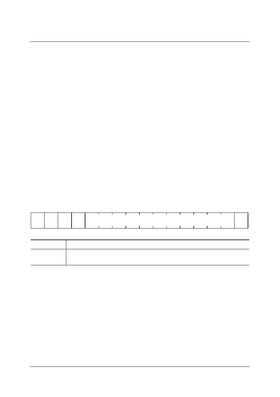
SDA 6000 / SDA 6001
PRELIMINARY DATA SHEET
Version 3.00
C16X Microcontroller
4 - 54
Micronas
stack may have been overwritten by the status information stacked upon the stack
overflow trap service.
� Automatic system stack flushing allows the use of the system stack as a "Stack
Cache" for a bigger external user stack. In this case the STKOV register should be
initialized to a value which represents the desired lowest Top of Stack address plus
12 according to the selected maximum stack size. This takes into consideration the
worst case that could occur, when a stack overflow condition is only detected during
entry into an interrupt service routine. Then, six additional stack word locations are
required to push IP, PSW, and CSP for both the interrupt service routine and the
hardware trap service routine.
The Stack Underflow Pointer STKUN
This non-bit addressable register is compared against the SP register after each
operation, which pops data from the system stack (e.g. POP and RET instructions) and
after each addition to the SP register. If the content of the SP register is greater than the
content of the STKUN register, a stack underflow hardware trap will occur.
Since the least significant bit of register STKUN is tied to `0' and bits 15 through 12 are
tied to `1' by hardware, the STKUN register can only contain values from F000
H
to
FFFE
H
.
STKUN
Reset Value: FC00
H
The Stack Underflow Trap (entered when (SP) > (STKUN)) may be used in two different
ways:
� Fatal error indication treats the stack underflow as a system error through the
associated trap service routine.
� Automatic system stack refilling allows the use of the system stack as a "Stack
Cache" for a bigger external user stack. In this case the STKUN register should be
initialized to a value which represents the desired highest Bottom of Stack address.
Scope of Stack Limit Control
The stack limit control, realized by the register pair STKOV and STKUN, detects cases
where the stack pointer SP is moved outside the defined stack area either by ADD or
Bit
Function
stkun
Modifiable portion of register STKUN
Specifies the upper limit of the internal system stack.
1
0
1
5
4
3
2
1
0
11
10
9
8
7
6
15
14
13
12
r
rw
r
r
r
1
1
r
stkun
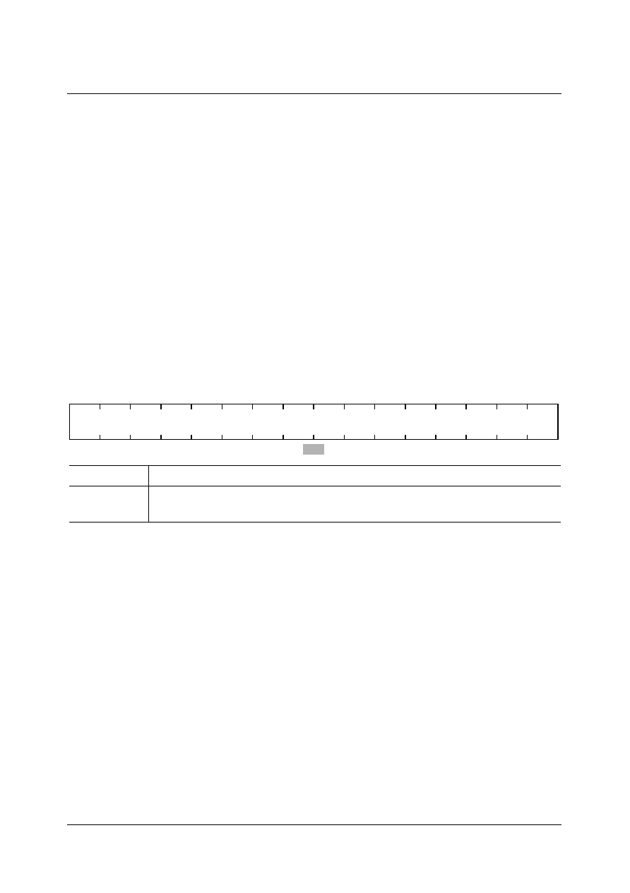
SDA 6000 / SDA 6001
PRELIMINARY DATA SHEET
Version 3.00
C16X Microcontroller
4 - 55
Micronas
SUB instructions or by PUSH or POP operations (explicit or implicit, i.e. CALL or RET
instructions).
This control mechanism is not triggered, i.e. no stack trap is generated, when
� the stack pointer SP is directly updated via MOV instructions
� the limits of the stack area (STKOV, STKUN) are changed, so that SP is outside of the
new limits.
The Multiply/Divide High Register MDH
This register is a part of the 32-bit multiply/divide register, which is implicitly used by the
CPU, when it performs a multiplication or a division. After a multiplication, this non-bit
addressable register represents the high order 16 bits of the 32-bit result. For long
division, the MDH register must be loaded with the high order 16 bits of the 32-bit
dividend before the division is started. After any division, the MDH register represents
the 16-bit remainder.
MDH
Reset Value: 0000
H
Whenever this register is updated via software, the Multiply/Divide Register In Use
(MDRIU) flag in the Multiply/Divide Control register (MDC) is set to `1'.
When multiplication or division is interrupted before its completion and when a new
multiply or divide operation is to be performed within the interrupt service routine, the
MDH register must be saved along with the MDL and MDC registers to avoid erroneous
results.
The Multiply/Divide Low Register MDL
This register is a part of the 32-bit multiply/divide register which is implicitly used by the
CPU when it performs a multiplication or a division. After multiplication, this non-bit
addressable register represents the low order 16 bits of the 32-bit result. For long
division, the MDL register must be loaded with the low order 16 bits of the 32-bit dividend
before the division is started. After any division, the MDL register represents the 16-bit
quotient.
Bit
Function
mdh
Specifies the high order 16 bits of the 32-bit multiply and divide register
MD.
5
4
3
2
1
0
11
10
9
8
7
6
15
14
13
12
rw
mdh
SDA 6000 / SDA 6001
PRELIMINARY DATA SHEET
Version 3.00
C16X Microcontroller
4 - 56
Micronas
MDL
Reset Value: 0000
H
Whenever this register is updated via software, the Multiply/Divide Register In Use
(MDRIU) flag in the Multiply/Divide Control register (MDC) is set to `1'. The MDRIU flag
is cleared whenever the MDL register is read via software.
When multiplication or division is interrupted before its completion and when a new
multiply or divide operation is to be performed within the interrupt service routine, the
MDL register must be saved along with the MDH and MDC registers to avoid erroneous
results.
The Multiply/Divide Control Register MDC
This bit addressable 16-bit register is implicitly used by the CPU when it performs
multiplication or division. It is used to store the required control information for the
corresponding multiply or divide operations. The MDC register is updated by hardware
during each single cycle of a multiply or divide instruction.
MDC
Reset Value: 0000
H
When division or multiplication is interrupted before its completion and the multiply/divide
unit is required, the MDC register must first be saved along with the MDH and MDL
Bit
Function
mdl
Specifies the low order 16 bits of the 32-bit multiply and divide register
MD.
Bit
Function
MDRIU
Multiply/Divide Register In Use
`0':
Cleared, when register MDL is read via software.
`1':
Set when the MDL or MDH register is written via software, or when
a multiply or divide instruction is executed.
!!
Internal Machine Status
The multiply/divide unit uses these bits to control internal operations.
Never modify these bits without saving and restoring the MDC register.
5
4
3
2
1
0
11
10
9
8
7
6
15
14
13
12
rw
mdl
-
!!
-
5
4
3
2
1
0
11
10
9
8
7
6
15
14
13
12
-
r(w)
-
-
-
-
-
-
-
-
!!
!!
!!
!!
!!
!!
-
-
-
-
r(w) r(w) r(w)
r(w) r(w) r(w) r(w)
MDR
IU

SDA 6000 / SDA 6001
PRELIMINARY DATA SHEET
Version 3.00
C16X Microcontroller
4 - 57
Micronas
registers (to be able to restart the interrupted operation later), and then it must be cleared
to prepare it for the new calculation. After the completion of the new division or
multiplication the state of the interrupted multiply or divide operation must be restored.
The MDRIU flag is the only portion of the MDC register which might be of interest to the
user. The remaining portions of the MDC register are reserved for dedicated use by the
hardware, and should never be modified by the user in any way other than described
above. Otherwise a correct continuation of an interrupted multiply or divide operation
cannot be guaranteed.
The Constant Zeros Register ZEROS
All bits of this bit-addressable register are fixed to `0' by hardware. This register can be
read only. The ZEROS register can be used as a register-addressable constant of all
zeros, i.e. for bit manipulation or mask generation. It can be accessed via any instruction
which is capable of addressing an SFR.
ZEROS
Reset Value: 0000
H
The Constant Ones Register ONES
All bits of this bit-addressable register are fixed to `1' by hardware. This register can be
read only. The ONES register can be used as a register-addressable constant of all
ones, i.e. for bit manipulation or mask generation. It can be accessed via any instruction
which is capable of addressing an SFR.
ONES (FF1E
H
/ 8F
H
)
Reset Value: FFFF
H
Note: Register SYSCON cannot be changed after execution of the EINIT instruction.
Identification Register Block
All new derivatives of 16-bit microcontrollers provide a set of identification registers that
offer information on the HW-status of the chip.The ID registers are read only registers.
They are placed in the extended SFR area.
0
0
0
0
0
5
4
3
2
1
0
11
10
9
8
7
6
15
14
13
12
r
r
r
r
r
r
0
0
0
r
0
0
0
0
0
0
0
0
r
r
r
r
r
r
r
r
r
1
1
1
1
1
5
4
3
2
1
0
11
10
9
8
7
6
15
14
13
12
r
r
r
r
r
r
1
1
1
r
1
1
1
1
1
1
1
1
r
r
r
r
r
r
r
r
r
SDA 6000 / SDA 6001
PRELIMINARY DATA SHEET
Version 3.00
C16X Microcontroller
4 - 58
Micronas
IDCHIP
IDMANUF
Bit
Function
CHIPREVNU
(7 ... 0)
Device Revision Code
Identifies the device step where the first release is marked `01
H
'.
CHIPID
(7 ... 0)
Device Identification
Identifies the device name.
Bit
Function
MANUF
JEDEC Normalized Manufacturer Code
0C1
H
: Infineon Technologies
5
4
3
2
1
0
11
10
9
8
7
6
15
14
13
12
r
r
CHIPID(7..0)
CHIPREVNU(7..0)
5
4
3
2
1
0
11
10
9
8
7
6
15
14
13
12
r
MANUF
-
-
-
-

Interrupt and Trap Function

SDA 6000 / SDA 6001
PRELIMINARY DATA SHEET
Version 3.00
Interrupt and Trap Functions
5 - 3
Micronas
5
Interrupt and Trap Functions
The C166 architecture supports several mechanisms for fast and flexible response to
service requests that can be generated from various sources either by the CPU itself or
external, i.e. peripherals connected to the XBUS or the PD bus.
These mechanisms include:
Normal Interrupt Processing
The CPU temporarily suspends the current program execution and branches to an
interrupt service routine in order to service an interrupt requesting device. The current
program status (IP, PSW, also CSP in segmentation mode) is saved on the internal
system stack. A prioritization scheme with 16 priority levels allows the user to specify the
order in which multiple interrupt requests are to be handled.
Interrupt Processing via the Peripheral Event Controller (PEC)
A faster alternative to normal software controlled interrupt processing is to service an
interrupt requesting device with the integrated Peripheral Event Controller (PEC).
Triggered by an interrupt request, the PEC performs a single word or byte data transfer
between any two locations in the whole memory space through one of nine
programmable PEC Service Channels. During a PEC transfer the normal program
execution of the CPU is halted for just 1 instruction cycle. No internal program status
information needs to be saved. The same prioritization scheme is used for PEC service
as for normal interrupt processing. PEC transfers share the 2 highest priority levels.
M2 enhances the functionalities of the original C166 PEC with the following features:
� PEC range extended to the entire memory space,
� new chaining mechanism between pairs of PEC channels.
Trap Functions
Trap functions are activated in response to special conditions that occur during the
execution of instructions. Several hardware trap functions are provided for handling
erroneous conditions and exceptions that arise during the execution of an instruction.
Hardware traps always have highest priority and cause immediate system reaction. The
software trap function is invoked by the TRAP instruction, which generates a software
interrupt for a specified interrupt vector. For all types of traps the current program status
is saved on the system stack.

SDA 6000 / SDA 6001
PRELIMINARY DATA SHEET
Version 3.00
Interrupt and Trap Functions
5 - 4
Micronas
5.1
Interrupt System Structure
M2 provides up to 33 separate interrupt nodes that may be assigned to 16 priority levels.
Each node is associated with an interrupt input line in the Interrupt System Interface of
the CPU. In order to support modular and consistent software design techniques, all
interrupt nodes are supplied with a separate interrupt control register and interrupt
vector. The control register contains the interrupt request flag, the interrupt enable bit,
and the interrupt priority of the associated node.
The C166 architecture provides a vectored interrupt system. In this system specific
vector locations in the memory space are reserved for the reset, trap, and interrupt
service functions. Whenever a request occurs, the CPU branches to the location that is
associated with the respective interrupt source. This allows direct identification of the
source that caused the request. The only exceptions are the class B hardware traps,
which all share the same interrupt vector. The status flags in the Trap Flag Register
(TFR) can then be used to determine which exception caused the trap. For the special
software TRAP instruction, the vector address is specified by the operand field of the
instruction, which is a seven bit trap number.
The reserved vector locations build a jump table in the low end of the address space
(segment 0). The jump table is made up of the appropriate jump instructions that transfer
control to the interrupt or trap service routines, which may be located anywhere within
the address space. The entries of the jump table are located at the lowest addresses in
code segment 0 of the address space. Each entry occupies 2 words, except for the reset
vector and the hardware trap vectors which occupy 4 or 8 words.
5.1.1
Interrupt Allocation Table
M2 provides 33 separate interrupt nodes that may be assigned to 16 priority levels. In
addition to the standard peripheral and external interrupts, there are some teletext
related interrupts which support the realtime processing of the sliced data and the
generation of the graphical data. Its fast external interrupt inputs are sampled every 3 ns
and are even able to recognize very short external signals.
The Table 5-1 lists all sources that are capable of requesting interrupt or PEC service in
M2, the associated interrupt vectors, their locations and the associated trap numbers. It
also lists the mnemonics of the affected interrupt request flags and their corresponding
interrupt enable flags. The mnemonics are composed of a part that specifies the
respective source, followed by a part that specifies their function (IR = Interrupt Request
flag, IE = Interrupt Enable flag).

SDA 6000 / SDA 6001
PRELIMINARY DATA SHEET
Version 3.00
Interrupt and Trap Functions
5 - 5
Micronas
Table 5-1
Interrupt Allocation Table
Source of Interrupt or PEC
Service Request
Interrupt
Control
Register
Address of
Control
Register
Interrupt
Vector
Location
Trap
Number
External Interrupt 0
EX0IC
00'FF88
H
00'0060
H
18
H
/24
D
External Interrupt 1
EX1IC
00'FF8A
H
00'0064
H
19
H
/25
D
External Interrupt 2
EX2IC
00'FF8C
H
00'0068
H
1A
H
/26
D
External Interrupt 3
EX3IC
00'FF8E
H
00'006C
H
1B
H
/27
D
External Interrupt 4
EX4IC
00'FF90
H
00'0070
H
1C
H
/28
D
External Interrupt 5
EX5IC
00'FF92
H
00'0074
H
1D
H
/29
D
External Interrupt 6
EX6IC
00'FF94
H
00'0078
H
1E
H
/30
D
External Interrupt 7
EX7IC
00'FF96
H
00'007C
H
1F
H
/31
D
GPT1 Timer 2
T2IC
00'FF60
H
00'0088
H
22
H
/34
D
GPT1 Timer 3
T3IC
00'FF62
H
00'008C
H
23
H
/35
D
GPT1 Timer 4
T4IC
00'FF64
H
00'0090
H
24
H
/36
D
GPT2 Timer 5
T5IC
00'FF66
H
00'0094
H
25
H
/37
D
GPT2 Timer 6
T6IC
00'FF68
H
00'0098
H
26
H
/38
D
GPT2 CAPREL Register
CRIC
00'FF6A
H
00'009C
H
27
H
/39
D
A/D1 Conversion Complete
ADC1IC
00'FF98
H
00'00A0
H
28
H
/40
D
A/D2 Conversion Complete
ADC2IC
00'FF9A
H
00'00A4
H
29
H
/40
D
ASC0 Transmit
S0TIC
00'FF6C
H
00'00A8
H
2A
H
/42
D
ASC0 Transmit Buffer
S0TBIC
00'F19C
H
00'011C
H
47
H
/71
D
ASC0 Receive
S0RIC
00'FF6E
H
00'00AC
H
2B
H
/43
D
ASC0 Autobaud Detection Start ABSTAIC
00'FF9E
H
00'0084
H
21
H
/33
D
ASC0 Autobaud Detection Stop ABSTOIC
00'F17A
H
00'00F4
H
3D
H
/61
D
ASC0 Error
S0EIC
00'FF70
H
00'00B0
H
2C
H
/44
D
SSC Transmit
SSCTIC
00'FF72
H
00'00B4
H
2D
H
/45
D
SSC Receive
SSCRIC
00'FF74
H
00'00B8
H
2E
H
/46
D
SSC Error
SSCEIC
00'FF76
H
00'00BC
H
2FH/47
D
I
2
C Data Transfer Event
I
2
CTIC
00'F194
H
00'0118
H
46
H
/70
D
I
2
C Protocol Event
I
2
CPIC
00'F18C
H
00'0114
H
45
H
/69
D
I
2
C Transmission End Event
I
2
CTEIC
00'F184
H
00'0110
H
44
H
/68
D

SDA 6000 / SDA 6001
PRELIMINARY DATA SHEET
Version 3.00
Interrupt and Trap Functions
5 - 6
Micronas
Note: Each entry of the interrupt vector table provides room for two word instructions or
one doubleword instruction. The respective vector location results from multiplying
the trap number by 4 (4 bytes per entry).
Note: * = Interrupts relevant for acquisition and graphic support.
5.1.2
Hardware Traps
The Table 5-2 lists the vector locations for hardware traps and the corresponding status
flags in the TFR register. It also lists the priorities of trap service for cases where more
than one trap condition might be detected within the same instruction. After any reset,
program execution starts at the reset vector at location 00'0000
H
. Reset conditions have
priority over every other system activity and therefore have the highest priority (trap
priority IV).
Software traps may be initiated to any vector location between 00'0000
H
and 00'01FC
H
.
A service routine entered via a software TRAP instruction is always executed on the
current CPU priority level which is indicated in bit field ILVL in register PSW. This means
that routines entered via the software TRAP instruction can be interrupted by all
hardware traps or higher level interrupt requests.
ADC Wake Up
ADWIC
00'F178
H
00'00F0
H
3C
H
/60
D
ACQ Interrupt *
ACQIC
00'F176
H
00'00EC
H
3B
H
/59
D
Display Vertical Sync *
VSDISIC
00'F174
H
00'00E8
H
3A
H
/58
D
Display Horizontal Sync *
HSDISIC
00'F172
H
00'00E4
H
39
H
/57
D
Graphic Acc. Finished *
GAFIC
00'FF9C
H
00'0080
H
20
H
/32
D
Realtime Clock
RTCIC
00'F19E
H
00'010C
H
43
H
/67
D
PECC Link IRQ
PECCLIC
00'F180
H
00'004C
H
4C
H
/76
D
Table 5-1
Interrupt Allocation Table (cont'd)
Source of Interrupt or PEC
Service Request
Interrupt
Control
Register
Address of
Control
Register
Interrupt
Vector
Location
Trap
Number

SDA 6000 / SDA 6001
PRELIMINARY DATA SHEET
Version 3.00
Interrupt and Trap Functions
5 - 7
Micronas
Normal Interrupt Processing and PEC Service
During each instruction cycle one out of all sources which require PEC or interrupt
processing is selected according to its interrupt priority. This prioritization of interrupts
and PEC requests is programmable in two levels. Each requesting source can be
assigned to a specific priority. A second level (called "group priority") allows the
specification of an internal order for simultaneous requests from a group of different
sources on the same priority level. At the end of each instruction cycle the one source
request with the highest current priority will be determined by the interrupt system. This
request will then be serviced if its priority is higher than the current CPU priority in the
PSW register.
Table 5-2
Exception Condition
Trap
Flag
Trap
Vector
Vector
Location
Trap
Number
Trap
Priority
Reset Functions:
Hardware Reset
Software Reset
Watchdog Timer
Overflow
�
RESET
RESET
RESET
00'0000
H
00'0000
H
00'0000
H
00
H
00
H
00
H
IV
IV
IV
Debug Hardware Trap
DEBUG
DTRAP
00'0020
H
08
H
III
Class A Hardware Traps:
Non-Maskable Interrupt
Stack Overflow
Stack Underflow
NMI
STKOF
STKUF
NMITRAP
STOTRAP
STUTRAP
00'0008
H
00'0010
H
00'0018
H
02
H
04
H
06
H
II
II
II
Class B Hardware Traps:
Undefined Opcode
Protected Instruction
Fault
Illegal Word Operand
Access
Illegal Instruction Access
Illegal External Bus
Access
UNDOPC
PRTFLT
ILLOPA
ILLINA
ILLBUS
BTRAP
BTRAP
BTRAP
BTRAP
BTRAP
00'0028
H
00'0028
H
00'0028
H
00'0028
H
00'0028
H
0A
H
0A
H
0A
H
0A
H
0A
H
I
I
I
I
I
Reserved
�
�
[2C
H
� 3C
H
] [0B
H
� 0F
H
] �
Software Traps
TRAP Instruction
�
�
Any
[00'0000
H
�
00'01FC
H
]
in steps
of 4
H
Any
[00
H
� 7F
H
]
Current
CPU
Priority

SDA 6000 / SDA 6001
PRELIMINARY DATA SHEET
Version 3.00
Interrupt and Trap Functions
5 - 8
Micronas
Interrupt System Register
Description Interrupt processing is controlled globally by the PSW register through a
general interrupt enable bit (IEN) and the CPU priority field (ILVL). Additionally the
different interrupt sources are controlled individually by their specific interrupt control
registers (... IC). Thus, the acceptance of requests by the CPU is determined by both the
individual interrupt control registers and the PSW. PEC services are controlled by the
respective PECCx register and the source and destination pointers, which specify the
task of the respective PEC service channel.
Interrupt Control Registers
All interrupt control registers are organized identically. The lower 8 bits of an interrupt
control register contain the complete interrupt status information of the associated
source which is required during one round of prioritization; the upper 8 bits of the
respective register are reserved. All interrupt control registers are bit-addressable and
all bits can be read or written via software. This allows each interrupt source to be
programmed or modified with just one instruction. When accessing interrupt control
registers through instructions which operate on word data types, their upper 8 bits
(15 ... 8) will return zeros when read, and will discard written data.
Note: The layout of the Interrupt Control registers shown below applies to each xxIC
register, where xx stands for the mnemonic for the respective source.
Interrupt Node Sharing
The interrupt controller of M2 can be configured to control up to 33 different sources. If
there is a need for a greater number of interrupt sources to be managed, interrupt
requests may share the same interrupt node. In this case, all the sources on the same
node share the priority level defined by the corresponding Interrupt Control register xxIC
and may be globally enabled/disabled by the IE bit of this register.
Arbitration between sources connected to the same node must be performed by the
interrupt handler associated with this node. For low rate requests, the software overhead
is not critical.

SDA 6000 / SDA 6001
PRELIMINARY DATA SHEET
Version 3.00
Interrupt and Trap Functions
5 - 9
Micronas
xxIC
Reset Value: - - 00
H
The Interrupt Request Flag is set by hardware whenever a service request from the
respective source occurs. It is cleared automatically upon entry into the interrupt service
routine or upon a PEC service. In the case of PEC service, the Interrupt Request flag
remains set if the COUNT field in register PECCx of the selected PEC channel
decrements to zero. This allows a normal CPU interrupt to respond to a completed PEC
block transfer.
Note: Modifying the Interrupt Request flag via software causes the same effect as if it
had been set or cleared by hardware.
Interrupt Priority Level and Group Level
The four bits of an ILVL bit field specify the priority level of a service request for the
arbitration of simultaneous requests. The priority increases with the numerical value of
ILVL, so 0000
B
is the lowest and 1111
B
is the highest priority level.
When more than one interrupt request on a specific level becomes active at the same
time, the values in the respective GLVL bit fields are used for second level arbitration to
select one request for servicing. Again the group priority increases with the numerical
value of GLVL, so 00
B
is the lowest and 11
B
is the highest group priority.
Bit
Function
GLVL
Group Level
Defines the internal order for simultaneous requests of the same priority.
3: Highest
group
priority
0:
Lowest group priority
ILVL
Interrupt Priority Level
Defines the priority level for the arbitration of requests.
F
H
: Highest priority level
0
H
: Lowest
priority
level
xxIE
Interrupt Enable Control Bit (individually enables/disables a specific
source)
`0': Interrupt request is disabled
`1': Interrupt Request is enabled
xxIR
Interrupt Request Flag
`0': No request pending
`1': This source has raised an interrupt request
5
4
3
2
1
0
11
10
9
8
7
6
15
14
13
12
rw
rw
-
-
-
-
rw
rw
-
-
-
-
xxIE
xxIR
GLVL
ILVL

SDA 6000 / SDA 6001
PRELIMINARY DATA SHEET
Version 3.00
Interrupt and Trap Functions
5 - 10
Micronas
Note: All interrupt request sources that are enabled and programmed to the same
priority level must always be programmed to different group priorities. Otherwise
an incorrect interrupt vector will be generated.
Upon entry into the interrupt service routine the priority level of the source that won the
arbitration and who's priority level is higher than the current CPU level, is copied into the
ILVL bit field of register PSW after pushing the old PSW contents onto the stack.
The interrupt system of M2 allows nesting of up to 15 interrupt service routines of
different priority levels (level 0 cannot be arbitrated).
Interrupt requests that are programmed to priority levels 15 or 14 (i.e., ILVL = 111X
B
) will
be serviced by the PEC unless the COUNT field of the associated PECC register
contains zero. In this case the request will instead be serviced by normal interrupt
processing. Interrupt requests that are programmed to priority levels 13 through 1 will
always be serviced by normal interrupt processing.
Note: Priority level 0000
B
is the default level of the CPU. Therefore a request on level 0
will never be serviced, because it can never interrupt the CPU. However, an
enabled interrupt request on level 0000
B
will terminate the Idle mode and
reactivate the CPU.
For interrupt requests which are to be serviced by the PEC, the associated PEC channel
number is derived from the respective ILVL (LSB) and GLVL (see Figure 5-1). So
programming a source to priority level 15 (ILVL = 1111
B
) selects the PEC channel group
7 ... 4, programming a source to priority level 14 (ILVL = 1110
B
) selects the PEC
channel group 3 ... 0. The actual PEC channel number is then determined by the GLVL
group priority field.
Figure 5-1
Priority Levels and PEC Channels
Simultaneous requests for PEC channels are prioritized according to the PEC channel
number, where channel 0 has lowest and channel 8 has highest priority.
Note: All sources that request PEC service must be programmed to different PEC
channels. Otherwise an incorrect PEC channel may be activated.
PEC Control
Interrupt
Control Register
ILVL
UED11127
PEC Channel #
GLVL

SDA 6000 / SDA 6001
PRELIMINARY DATA SHEET
Version 3.00
Interrupt and Trap Functions
5 - 11
Micronas
The table below shows a few examples of each action executed with each particular
programming of an interrupt control register.
Note: All requests on levels 13 ... 1 cannot initiate PEC transfers. They are always
serviced by an interrupt service routine. No PECC register is associated and no
COUNT field is checked.
Interrupt Control Functions in the PSW
The Processor Status Word (PSW) is functionally divided into 2 parts: the lower byte of
the PSW basically represents the arithmetic status of the CPU, the upper byte of the
PSW controls the interrupt system of M2 and the arbitration mechanism for the external
bus interface.
Note: Pipeline effects have to be considered when enabling/disabling interrupt requests
via modifications of register PSW.
Priority Level
Type of Service
ILVL
GLVL
COUNT = 00
H
COUNT
00
H
1 1 1 1
1 1
CPU interrupt,
level 15, group priority 3
PEC service,
channel 7
1 1 1 1
1 0
CPU interrupt,
level 15, group priority 2
PEC service,
channel 6
1 1 1 0
1 0
CPU interrupt,
level 14, group priority 2
PEC service,
channel 2
1 1 0 1
1 0
CPU interrupt,
level 13, group priority 2
CPU interrupt,
level 13, group priority 2
0 0 0 1
1 1
CPU interrupt,
level 1, group priority 3
CPU interrupt,
level 1, group priority 3
0 0 0 1
0 0
CPU interrupt,
level 1, group priority 0
CPU interrupt,
level 1, group priority 0
0 0 0 0
X X
No service!
No service!
SDA 6000 / SDA 6001
PRELIMINARY DATA SHEET
Version 3.00
Interrupt and Trap Functions
5 - 12
Micronas
PSW
Reset Value: 0000
H
CPU Priority ILVL defines the current level for the operation of the CPU. This bit field
reflects the priority level of the routine that is currently being executed. Upon entry into
an interrupt service routine, this bit field is updated with the priority level of the request
that is being serviced. The PSW is saved on the system stack before. The CPU level
determines the minimum interrupt priority level that will be serviced. Any request on the
same or lower level will not be acknowledged.
The current CPU priority level may be adjusted via software, to control which interrupt
request sources will be acknowledged.
PEC transfers do not really interrupt the CPU, but rather "steal" a single cycle, so PEC
services do not influence the ILVL field in the PSW.
Hardware traps switch the CPU level to maximum priority (i.e. 15) so no interrupt or PEC
requests will be acknowledged while an exception trap service routine is being executed.
Note: The TRAP instruction does not change the CPU level, so software invoked trap
service routines may be interrupted by higher requests.
Interrupt Enable bit IEN globally enables or disables PEC operations and the
acceptance of interrupts by the CPU. When IEN is cleared, no new interrupt requests are
Bit
Function
N, C, V, Z, E,
MULIP,
USR0
CPU status flags (Described in Chapter 4.6)
Define the current status of the CPU (ALU, multiplication unit).
HLDEN
HOLD Enable (Enables External Bus Arbitration)
0:
Bus arbitration disabled, P6.7 ... P6.5 may be used for general
purpose IO
1:
Bus arbitration enabled, P6.7 ... P6.5 serve as BREQ, HLDA,
HOLD, resp.
ILVL
CPU Priority Level
Defines the current priority level for the CPU
F
H
: Highest priority level
0
H
: Lowest
priority
level
IEN
Interrupt Enable Control Bit (globally enables/disables interrupt
requests)
`0': Interrupt requests are disabled
`1': Interrupt requests are enabled
HLD
EN
-
MUL
IP
USR0
N
Z
C
V
E
5
4
3
2
1
0
11
10
9
8
7
6
15
14
13
12
rw
rw
rw
rw
-
rw
rw
rw
-
rw
-
rw
IEN
-
-
ILVL
rw

SDA 6000 / SDA 6001
PRELIMINARY DATA SHEET
Version 3.00
Interrupt and Trap Functions
5 - 13
Micronas
accepted by the CPU. However requests that have already entered the pipeline at that
time will be processed. When IEN is set to `1', all interrupt sources, which have been
individually enabled by the interrupt enable bits in their associated control registers, are
globally enabled.
Note: Traps are non-maskable and are therefore not affected by the IEN bit.
SDA 6000 / SDA 6001
PRELIMINARY DATA SHEET
Version 3.00
Interrupt and Trap Functions
5 - 14
Micronas
5.2
Operation of the PEC Channels
M2's Peripheral Event Controller (PEC) provides 8 PEC service channels, which move
a single byte or word between two locations in the entire memory space. Packet
transfers are provided with channels 0 and 1. This is the fastest possible interrupt
response and in many cases is sufficient to service the respective peripheral request
(e.g. serial channels, etc.). Each channel is controlled by a dedicated PEC Channel
Counter/Control register (PECCx) and a pair of pointers for the source (SRCPx) and
destination (DSTPx) of the data transfer.
The PECC registers control the action that is performed by the respective PEC channel.
Compared to existing C16x architectures, the PEC transfer function is enhanced by
extended functionality. The extended PEC functions are defined as follows:
� Source pointer and destination pointer are extended to 24-bit pointer, thus enabling
PEC controlled data transfers between any two locations within the total address
space. Both 8-bit segment numbers of every source/destination pointer pair are
defined in one 16-bit SFR register; thus, 8 PEC segment number registers are
available for the 8 PEC channels.
� For every two channels a chaining feature is provided. When enabled in the PEC
control register, a termination interrupt of one channel will automatically switch
transfer control to the other channel of the channel pair.
Extended PEC Channel Control
The PEC control registers with the extended functionality and their application for new
PEC control are defined as follows:
PECCx
Reset Value: 0000
H
Bit
Function
COUNT
(7 ... 0)
PEC Transfer Count
Counts PEC transfers (bytes or words) and influences the channel's
action.
BWT
Byte / Word Transfer Selection
0: Transfer
a
Word.
1: Transfer
a
Byte.
5
4
3
2
1
0
11
10
9
8
7
6
15
14
13
12
rw
rw
-
-
-
CLT
CL
INC(1..0)
BWT
COUNT (7...0)
rw
rw
rw
SDA 6000 / SDA 6001
PRELIMINARY DATA SHEET
Version 3.00
Interrupt and Trap Functions
5 - 15
Micronas
Byte/Word Transfer bit BWT controls, if a byte or a word is moved during a PEC service
cycle. This selection controls the transferred data size and the increment step for the
modified pointer.
Increment Control Field INC controls, if one of the PEC pointers is incremented after
the PEC transfer. However, it is not possible to increment both pointers. If the pointers
are not modified (INC = `00') the respective channel will always move data from the
same source to the same destination.
Note: The reserved combination `11' is changed to `10' by hardware. However, it is not
recommended to use this combination.
The PEC Transfer Count Field COUNT controls the action of a respective PEC channel,
where the content of bit field COUNT, at the time the request is activated, selects the
action. COUNT may allow a specified number of PEC transfers, unlimited transfers or no
PEC service at all.
The table below summarizes, how the COUNT field itself, the interrupt requests flag IR
and the PEC channel action depends on the previous content of COUNT.
INC(1 ... 0)
Increment Control
(Modification of SRCPx or DSTPx)
0 0: Pointers are not modified.
0 1: Increment DSTPx by 1 or 2.
1 0: Increment SRCPx by 1 or 2.
1 1: Reserved. Do not use this combination.
CL
Channel Link Control
0: PEC
channels
work independent
1: Pairs
of
channels are linked together
CLT
Channel Link Toggle State
0:
Even numbered PEC channel of linked channels active
1:
Odd numbered PEC channel of linked channels active
Table 5-3
PEC Control Register Addresses
Register
Address
Reg. Space
Register
Address
Reg. Space
PECC0
FEC0
H
/ 60
H
SFR
PECC4
FEC8
H
/ 64
H
SFR
PECC1
FEC2
H
/ 61
H
SFR
PECC5
FECA
H
/ 65
H
SFR
PECC2
FEC4
H
/ 62
H
SFR
PECC6
FECC
H
/ 66
H
SFR
PECC3
FEC6
H
/ 63
H
SFR
PECC7
FECE
H
/ 67
H
SFR
Bit
Function

SDA 6000 / SDA 6001
PRELIMINARY DATA SHEET
Version 3.00
Interrupt and Trap Functions
5 - 16
Micronas
The PEC transfer counter allows the servicing of a specified number of requests by the
respective PEC channel, and then (when COUNT reaches 00
H
) activates the interrupt
service routine, which is associated with the priority level. After each PEC transfer the
COUNT field is decremented and the request flag is cleared to indicate that the request
has been serviced.
Continuous transfers are selected by the value FF
H
in bit field COUNT. In this case
COUNT is not modified and the respective PEC channel services any request until it is
disabled again.
When COUNT is decremented from 01
H
to 00
H
after a transfer the request flag is not
cleared, which generates another request from the same source. When COUNT already
contains the value 00
H
, the respective PEC channel remains idle and the associated
interrupt service routine is activated instead. This provides a choice if a level 15 or 14
request is to be serviced by the PEC or by the interrupt service routine.
Note: PEC transfers are only executed if their priority level is higher than the CPU level,
i.e. only PEC channels 7 ... 4 are processed, while the CPU executes on level 14.
All interrupt request sources that are enabled and programmed for PEC service
should use different channels. Otherwise only one transfer will be performed for
all simultaneous requests. When COUNT is decremented to 00
H
, and the CPU is
interrupted, an incorrect interrupt vector will be generated.
Channel Link Mode for Data Chaining
Data chaining with linked PEC channels is enabled if the channel link control bit in
PECCx register is set to `1' either in one or both PEC channel control registers of a
channel pair. In this case, two PEC channels are linked together and handle chained
block transfers alternatively to each other. The whole data transfer is divided into several
block transfers where each block is controlled by one PEC channel of a channel pair.
Previous
COUNT
Modified
COUNT
IR after PEC
service
Action of PEC Channel
and Comments
FF
H
FF
H
`0'
Move a Byte / Word
Continuous transfer mode, i.e. COUNT is not
modified
FE
H
... 02
H
FD
H
... 01
H
`0'
Move a Byte / Word and decrement COUNT
01
H
00
H
`1'
Move a Byte / Word
Leave request flag set, which triggers another
request
00
H
00
H
(`1')
No action!
Activate interrupt service routine rather than
PEC channel.

SDA 6000 / SDA 6001
PRELIMINARY DATA SHEET
Version 3.00
Interrupt and Trap Functions
5 - 17
Micronas
When a data block is completely transferred a channel link interrupt is generated and
the PEC service request processing is automatically switched to the "other" PEC channel
of the channel-pair. Thus, PEC service requests addressed to a linked PEC channel are
either handled by linked PEC channel A or by linked PEC channel B. This channel toggle
allows the setting up of shadow and multiple buffers for PEC transfers by changing
pointer and count values of one channel while the other channel is active. The following
table lists the channels that can be linked together, and the channel numbers to address
the linked channels.
For each pair of linked channels an internal channel flag, the channel link toggle flag
CLT, identifies which of the two PEC channels will serve the next PEC request. The CLT
flag is indicated in both PECCx registers of the two linked PEC channels, where the CLT
bit in channel B is always inverse to the CLT bit in channel A. The very first transfer is
always started with the channel A if the CLT bit is not otherwise programmed before. The
CLT bit is only valid in the case of linked PEC channels, indicated by the CL bits of linked
channels. If linking is not enabled, the CLT bit of both channels is always zero.
The internal channel link flag CLT toggles, and the other channel begins servicing with
the next request if the "old" channel stops the service (COUNT = 0), and if the new
channel has in its PEC control register the enabled CL flag and if its transfer count is
more than zero.
Note: With the last transfer of a block transfer (COUNT = 0), the channel link control flag
CL of that channel is cleared in its PECCx register. If the CL channel link flag of
the new (chained) PEC control register is found to be zero, the whole data transfer
is finished and the channel link interrupt is coincidentally a termination interrupt.
The channel link mode is finished and the internal channel toggle flag is cleared
after the last transfer of the block, if the CL flags of both pair channels are cleared.
Additional Interrupt Request Node for Channel Link Interrupts
The PEC unit has one dedicated service request node (trap number) for all channel link
interrupts. This service request node requests CPU interrupt service in case of one or
more channel link request flags and the respective enable control bit being set in the
channel link interrupt subnode control register (CLISNC). These flags indicate a channel
Linked PEC Channels
Linked PEC Channel
PEC Channel
A
PEC Channel
B
channel 0
channel 1
channel 0
channel 2
channel 3
channel 2
channel 4
channel 5
channel 4
channel 6
channel 7
channel 6

SDA 6000 / SDA 6001
PRELIMINARY DATA SHEET
Version 3.00
Interrupt and Trap Functions
5 - 18
Micronas
link interrupt condition of linked PEC channels (A and B channels) which requires
support from the CPU. The following channel link interrupt conditions requesting CPU
service are possible:
� In single transfer mode a COUNT value change from 01
H
to 00
H
in a linked PEC
channel and CL flag is set in the respective PEC control register.
In this case the CPU service is requested to update the PEC control and pointer registers
while the next block transfer is executed (the whole transfer is divided into separately
controlled block transfers). The last block transfer is determined by the missing link bit in
the new (linked) PEC control register. If a new service request hits a linked channel with
count equal to zero and channel link flag disabled, a standard interrupt, as known from
standard PEC channels, is performed.
The channel link interrupt subnode register CLISNC is defined as follows:
CLISNC Reset
Value:
0000
H
The source and destination pointers specifiy the locations between which the data is
to be moved. PEC transfers can be performed between any locations in the entire
memory space of the M2. For each of the 8 PEC channels, the source and destination
addresses are specified by a 8-bit segment number and a 16-bit offset. The source and
destination segment numbers, respectively PECSSN and PECDSN, are stored in a SFR
associated with each channel (PECSNx, see description below). The offset pointers for
the source and destination address do not reside in specific SFRs, but are mapped into
the internal RAM of the M2 just below the bit-addressable area (see Figure 5-2).
Bit
Function
xxIE
PEC Channel Link Interrupt Enable Control Bit
(individually enables/disables a specific channel pair interrupt request)
`0': PEC interrupt request is disabled
`1':
PEC interrupt request is enabled
xxIR
PEC Channel Service Request Flag
`0': No channel link service request pending
`1': This source (channel pair) has raised an request to service a PEC
channel after channel linking
5
4
3
2
1
0
11
10
9
8
7
6
15
14
13
12
rw
rw
rw
rw
rw
rw
rw
rw
-
-
C6
IR
C6
IE
-
-
C4
IR
C4
IE
-
-
C2
IR
C2
IE
-
-
C0
IR
C0
IE

SDA 6000 / SDA 6001
PRELIMINARY DATA SHEET
Version 3.00
Interrupt and Trap Functions
5 - 19
Micronas
Figure 5-2
Mapping of PEC Offset Pointers into the Internal RAM
The pointer locations for inactive PEC channels may be used for general data storage.
Only the required pointers occupy RAM locations.
PECSNx Reset
Value:
0000
H
Bit
Function
PECSSN
(7 ... 0)
PEC Source Segment Number
8-bit Segment Number (address bits A23 ... 16) used for addressing the
source of the respective PEC transfer.
PECDSN
(7 ... 0)
PEC Destination Segment Number
8-bit Segment Number (address bits A23 ... 16) used for addressing the
destination of the respective PEC transfer.
UED11128
00'FCFE
H
DSTP7
SRCP7
00'FCFC
H
DSTP6
00'FCFA
H
SRCP6
00'FCF8
H
DSTP5
00'FCF6
H
SRCP5
00'FCF4
H
DSTP4
00'FCF2
H
SRCP4
00'FCF0
H
00'FCE2
DSTP0
H
SRCP0
H
00'FCE0
SRCP1
DSTP1
SRCP2
DSTP2
SRCP3
DSTP3
H
H
H
H
00'FCE8
00'FCE4
00'FCE6
00'FCEC
00'FCEA
00'FCEE
H
H
5
4
3
2
1
0
11
10
9
8
7
6
15
14
13
12
rw
rw
PECDSN (7...0)
PECSSN (7...0)

SDA 6000 / SDA 6001
PRELIMINARY DATA SHEET
Version 3.00
Interrupt and Trap Functions
5 - 20
Micronas
If a word data transfer is selected for a specific PEC channel (i.e. BWT = `0'), the
respective source and destination pointers must both contain a valid word address which
points to an even byte boundary. Otherwise the Illegal Word Access trap will be invoked
when this channel is used.
5.2.1
Prioritization of Interrupt and PEC Service Requests
Interrupt and PEC service requests from all sources can be enabled so they are
arbitrated and serviced (if they win), or they may be disabled so their requests are
disregarded and not serviced.
Enabling and disabling interrupt requests may be done via three mechanisms:
Control Bits allow the switching of each individual source to "ON" or "OFF" so that it may
generate a request or not. The control bits (xxIE) are located in the respective interrupt
control registers. All interrupt requests can generally be enabled or disabled via the IEN
bit in register PSW. This control bit is the "main switch" that selects whether requests
from any source are accepted or not.
For a specific request to be arbitrated the respective source's enable bit and the global
enable bit must both be set.
The Priority Level automatically selects a certain group of interrupt requests that will be
acknowledged, disclosing all other requests. The priority level of the source that won the
arbitration is compared with the CPU's current level and the source is only serviced if its
level is higher than the current CPU level. Changing the CPU level to a specific value via
software blocks all requests on the same or a lower level. An interrupt source that is
assigned to level 0 will be disabled and never be serviced.
The ATOMIC and EXTend instructions automatically disable all interrupt requests for
the duration of the following 1 ... 4 instructions. This is useful e.g. for semaphore
handling and does not require re-enabling the interrupt system after the inseparable
instruction sequence.
Interrupt Class Management
An interrupt class covers a set of interrupt sources with the same importance, i.e. the
same priority from the system's viewpoint. Interrupts of the same class must not interrupt
each other. M2 supports this function with two features:
Table 5-4
PEC Segment Number Register Addresses
Register
Address
Reg. Space
Register
Address
Reg. Space
PECSN0
FED0
H
/ 68
H
SFR
PECSN4
FED8
H
/ 6C
H
SFR
PECSN1
FED2
H
/ 69
H
SFR
PECSN5
FEDA
H
/ 6D
H
SFR
PECSN2
FED4
H
/ 6A
H
SFR
PECSN6
FEDC
H
/ 6E
H
SFR
PECSN3
FED6
H
/ 6B
H
SFR
PECSN7
FEDE
H
/ 6F
H
SFR

SDA 6000 / SDA 6001
PRELIMINARY DATA SHEET
Version 3.00
Interrupt and Trap Functions
5 - 21
Micronas
Classes with up to 4 members can be established by using the same interrupt priority
(ILVL) and assigning a dedicated group level (GLVL) to each member. This functionality
is built-in and handled automatically by the interrupt controller.
Classes with more than 4 members can be established by using a number of adjacent
interrupt priorities (ILVL) and the respective group levels (4 per ILVL). Each interrupt
service routine within this class sets the CPU level to the highest interrupt priority within
the class. All requests from the same or any lower level are blocked now, i.e. no request
of this class will be accepted.
The example below establishes 3 interrupt classes which cover 2 or 3 interrupt priorities,
depending on the number of members in a class. A level 6 interrupt disables all other
sources in class 2 by changing the current CPU level to 8, which is the highest priority
(ILVL) in class 2. Class 1 requests or PEC requests are still serviced in this case.
The 24 interrupt sources (excluding PEC requests) are assigned to 3 classes of priority
rather than to 7 different levels, as the hardware support would do.
Table 5-5
Software controlled Interrupt Classes (Example)
ILVL
(Priority
GLVL
Interpretation
3
2
1
0
15
PEC service on up to 8 channels
14
13
12
X
X
X
X
Interrupt Class 1
5 sources on 2 levels
11
X
10
9
8
X
X
X
X
Interrupt Class 2
9 sources on 3 levels
7
X
X
X
X
6
X
5
X
X
X
X
Interrupt Class 3
5 sources on 2 levels
4
X
3
2
1
0
No service!
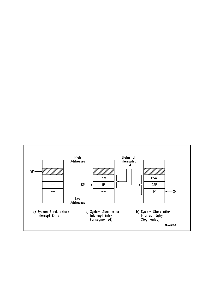
SDA 6000 / SDA 6001
PRELIMINARY DATA SHEET
Version 3.00
Interrupt and Trap Functions
5 - 22
Micronas
5.2.2
Saving the Status during Interrupt Service
Before an interrupt request that has been arbitrated is actually serviced, the status of the
current task is automatically saved on the system stack. The CPU status (PSW) is saved
along with the location, where the execution of the interrupted task is resumed after
returning from the service routine. This return location is specified through the Instruction
Pointer (IP) and, in case of a segmented memory model, the Code Segment Pointer
(CSP). Bit SGTDIS in register SYSCON controls how the return location is stored.
The system stack first receives the PSW, followed by the IP (unsegmented) or the CSP
and then IP (segmented mode). This optimizes the usage of the system stack, if
segmentation is disabled.
The CPU priority field (ILVL in PSW) is updated with the priority of the interrupt request
that is to be serviced, so the CPU now executes on the new level. If multiplication or
division was in progress at the time the interrupt request was acknowledged bit MULIP
in register PSW is set to `1'. In this case the return location that is saved on the stack is
not the next instruction in the instruction flow, but rather the multiply or divide instruction
itself, as this instruction has been interrupted and will be completed after returning from
the service routine.
Figure 5-3
Task Status Saved on the System Stack
The interrupt request flag of the source that is being serviced is cleared. The IP is loaded
with the vector associated with the requesting source (the CSP is cleared in case of
segmentation) and the first instruction of the service routine is fetched from the
respective vector location, which is expected to branch to the service routine itself. The
data page pointers and the context pointer are not affected.
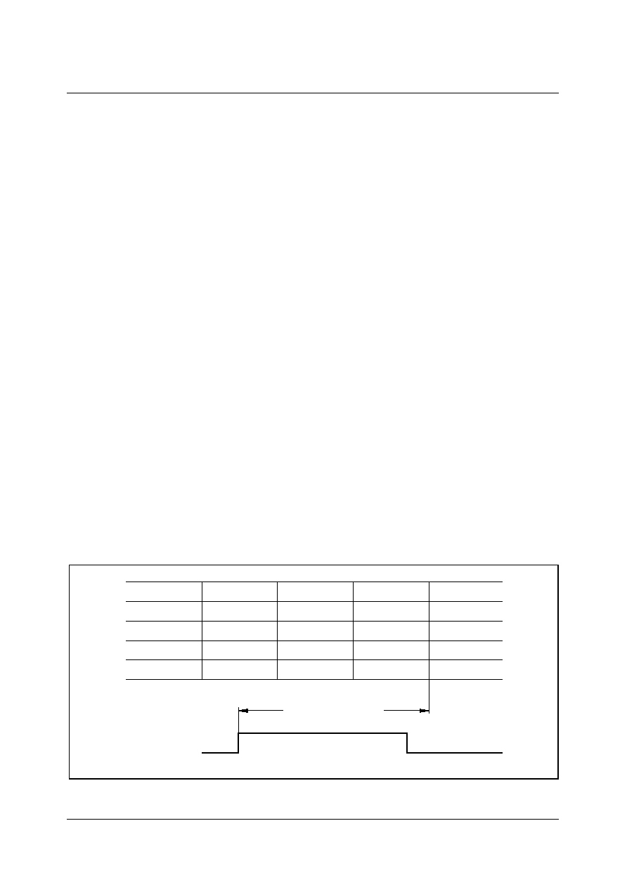
SDA 6000 / SDA 6001
PRELIMINARY DATA SHEET
Version 3.00
Interrupt and Trap Functions
5 - 23
Micronas
When the interrupt service routine is left (RETI is executed), the status information is
popped from the system stack in reverse order, taking into account the value of bit
SGTDIS.
Context Switching
An interrupt service routine usually saves all the registers it uses on the stack, and
restores them before returning. The more registers a routine uses, the more time is
wasted with saving and restoring. The M2 allows the complete bank of CPU registers
(GPRs) to switch with a single instruction, so the service routine executes within its own,
separate context.
The instruction "SCXT CP, #New_Bank" pushes the contents of the context pointer (CP)
on the system stack and loads CP with the immediate value "New_Bank", which selects
a new register bank. The service routine may now use its "own registers". This register
bank is preserved when the service routine terminates, i.e. its contents are available on
the next call.
Before returning (RETI) the previous CP is simply POPped from the system stack, which
returns the registers to the original bank.
Note: The first instruction following the SCXT instruction must not use a GPR.
Resources that are used by the interrupting program must eventually be saved and
restored, e.g. the DPPs and the registers of the MUL/DIV unit.
5.2.3
Interrupt Response Times
The interrupt response time defines the time from an interrupt request flag of an enabled
interrupt source being set until the first instruction (I1) is fetched from the interrupt vector
location. The basic interrupt response time for the M2 is 3 instruction cycles.
Figure 5-4
Pipeline Diagram for Interrupt Response Time
UED11129
IR-Flag
0
1
Interrupt Response Time
Pipeline Stage
FETCH
DECODE
EXECUTE
WRITEBACK
Cycle 1
Cycle 2
Cycle 3
Cycle 4
N
N - 1
N - 2
N - 3
N + 1
N
N - 1
N - 2
N + 2
TRAP (1)
N
N - 1
I1
TRAP (2)
TRAP
N

SDA 6000 / SDA 6001
PRELIMINARY DATA SHEET
Version 3.00
Interrupt and Trap Functions
5 - 24
Micronas
All instructions in the pipeline, including instruction N (during which the interrupt request
flag is set), are completed before entering the service routine. The actual execution time
for these instructions (e.g. wait-states) therefore influences the interrupt response time.
In Figure 5-4 the respective interrupt request flag is set in cycle 1 (the fetching of
instruction N). The indicated source wins the prioritization round (during cycle 2). In
cycle 3 a TRAP instruction is injected into the decode stage of the pipeline, replacing
instruction N+1 and clearing the source's interrupt request flag to `0'. Cycle 4 completes
the injected TRAP instruction (save PSW, IP and CSP, if in segmented mode) and
fetches the first instruction (I1) from the respective vector location.
All instructions that entered the pipeline, after the setting of the interrupt request flag
(N+1, N+2), will be executed after returning from the interrupt service routine.
The minimum interrupt response time is 5 states (10 TCL). This requires program
execution from the internal code memory, no external operand read requests and setting
the interrupt request flag during the last state of an instruction cycle. When the interrupt
request flag is set during the first state of an instruction cycle, the minimum interrupt
response time under these conditions is 6 state times (12 TCL).
The interrupt response time is increased by all delays of the instructions in the pipeline
that are executed before entering the service routine (including N).
� When internal hold conditions between instruction pairs N-2/N-1 or N-1/N occur, or
when instruction N explicitly writes to the PSW or the SP, the minimum interrupt
response time may be extended by 1 state time for each of these conditions.
� When instruction N reads an operand from the internal code memory, or when N is a
call, return, trap, or MOV Rn, [Rm+ #data16] instruction, the minimum interrupt
response time may be extended by 2 state times during internal code memory
program execution.
� In case instruction N reads the PSW and instruction N-1 effects the condition flags,
the interrupt response time may be extended by 2 state times.
The worst case interrupt response time during internal code memory program execution
adds 12 state times (24 TCL).
Any reference to external locations increases the interrupt response time due to pipeline
related access priorities. The following conditions have to be considered:
� Instruction fetch from an external location
� Operand read from an external location
� Result write-back to an external location
There are a number of combinations depending on where the instructions, source and
destination operands are located. Note, however, that only access conflicts contribute to
the delay.
A few examples illustrate these delays:
� The worst case interrupt response time, including external accesses, will occur when
instructions N, N+1 and N+2 are executed out of external memory, instructions N-1

SDA 6000 / SDA 6001
PRELIMINARY DATA SHEET
Version 3.00
Interrupt and Trap Functions
5 - 25
Micronas
and N require external operand read accesses, instructions N-3 through N write back
external operands, and the interrupt vector also points to an external location. In this
case the interrupt response time is the time needed to perform 9 word bus accesses,
because instruction I1 cannot be fetched via the external bus until all write, fetch and
read requests from preceding instructions in the pipeline are terminated.
� When the interrupt vector, of the example above, is pointing into the internal code
memory, the interrupt response time is 7 word bus accesses plus 2 states because
the fetching of instruction I1 from internal code memory can start earlier.
� When instructions N, N+1 and N+2 are executed out of the external memory and the
interrupt vector points to an external location, but all operands for instructions N-3
through N are in internal memory, then the interrupt response time is the time needed
to perform 3 word bus accesses.
� When the interrupt vector, of the example above, is pointing into the internal code
memory, the interrupt response time is 1 word bus access plus 4 states.
After an interrupt service routine has been terminated by executing the RETI instruction,
and if further interrupts are pending, the next interrupt service routine will not be entered
until at least two instruction cycles of the program that was interrupted have been
executed. In most cases two instructions will be executed during this time. Only one
instruction will typically be executed if the first instruction following the RETI instruction
is a branch instruction (without cache hit), if it reads an operand from internal code
memory, or if it is executed out of the internal RAM.
Note: A bus access, in this context, includes all delays which can occur during an
external bus cycle.
5.2.4
PEC Response Times
The PEC response time defines the time between an interrupt request flag of an enabled
interrupt source being set and the PEC data transfer being started. The basic PEC
response time for the M2 is 2 instruction cycles.
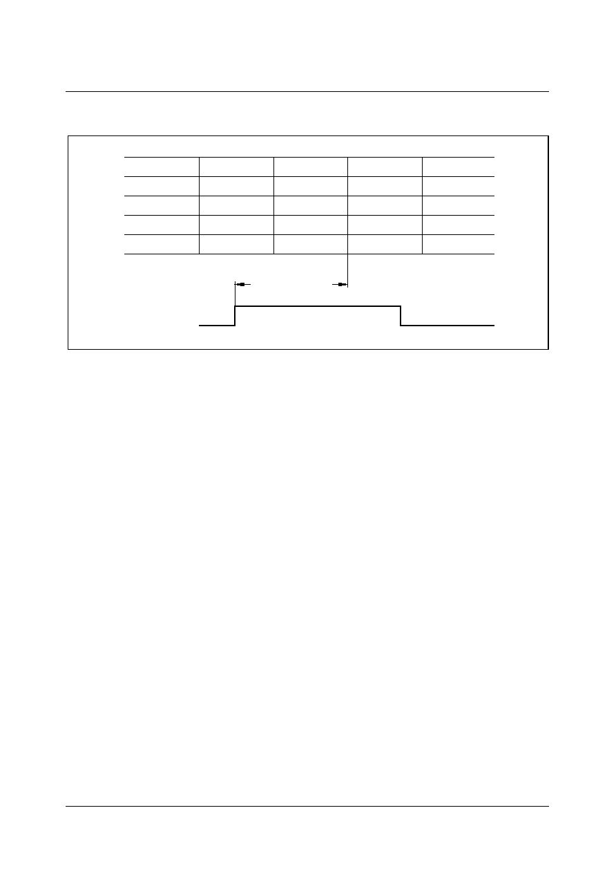
SDA 6000 / SDA 6001
PRELIMINARY DATA SHEET
Version 3.00
Interrupt and Trap Functions
5 - 26
Micronas
Figure 5-5
Pipeline Diagram for PEC Response Time
In Figure 5-5, the respective interrupt request flag is set in cycle 1 (fetching instruction
N). The indicated source wins the prioritization round (during cycle 2). In cycle 3 a PEC
transfer "instruction" is imported into the decode stage of the pipeline, suspending
instruction N+1 and clearing the source's interrupt request flag to `0'. Cycle 4 completes
the imported PEC transfer and resumes the execution of instruction N+1.
All instructions that entered the pipeline after setting of the interrupt request flag (N+1,
N+2) will be executed after the PEC data transfer.
Note: When instruction N reads any of the PEC control registers PECC7 ... PECC0,
while a PEC request wins the current round of prioritization, the round is repeated
and the PEC data transfer is started one cycle later.
The minimum PEC response time is 3 states (6 TCL). This requires program execution
from the internal code memory, no external operand read requests and setting the
interrupt request flag during the last state of an instruction cycle. When the interrupt
request flag is set during the first state of an instruction cycle, the minimum PEC
response time under these conditions is 4 state times (8 TCL).
The PEC response time is increased by all delays of the instructions in the pipeline which
are executed before starting the data transfer (including N).
� When internal hold conditions between instruction pairs N-2/N-1 or N-1/N occur, the
minimum PEC response time may be extended by 1 state time for each of these
conditions.
� When instruction N reads an operand from the internal code memory, or when N is a
call, return, trap, or MOV Rn, [Rm+ #data16] instruction, the minimum PEC response
time may be extended by 2 state times during internal code memory program
execution.
UED11130
IR-Flag
0
1
PEC Response Time
Pipeline Stage
FETCH
DECODE
EXECUTE
WRITEBACK
Cycle 1
Cycle 2
Cycle 3
Cycle 4
N
N - 1
N - 2
N - 3
N + 1
N
N - 1
N - 2
N + 2
PEC
N
N - 1
N + 2
N + 1
PEC
N

SDA 6000 / SDA 6001
PRELIMINARY DATA SHEET
Version 3.00
Interrupt and Trap Functions
5 - 27
Micronas
� If instruction N reads the PSW and instruction N-1 effects the condition flags, the PEC
response time may additionally be extended by 2 state times.
The worst case PEC response time during internal code memory program execution
adds to 9 state times (18 TCL).
Any reference to external locations increases the PEC response time due to pipeline
related access priorities. The following conditions have to be considered:
� Instruction fetch from an external location
� Operand read from an external location
� Result write-back to an external location
There are a number of combinations depending on where the instructions, source and
destination operands are located. Note, however, that only access conflicts contribute to
the delay.
A few examples illustrate these delays:
� The worst case interrupt response time, including external accesses, will occur when
instructions N and N+1 are executed out of external memory, instructions N-1 and N
require external operand read accesses and instructions N-3, N-2 and N-1 write back
external operands. In this case the PEC response time is the time needed to perform
7 word bus accesses.
� When instructions N and N+1 are executed out of the external memory, but all
operands for instructions N-3 through N-1 are in internal memory, then the PEC
response time is the time needed to perform 1 word bus access plus 2 state times.
Once a request for PEC service has been acknowledged by the CPU, the execution of
the next instruction is delayed by 2 state times plus the additional time it might take to
fetch the source operand from internal code memory or external memory and to write the
destination operand over the external bus in an external program environment.
Note: A bus access, in this context, includes all delays which can occur during an
external bus cycle.
For an EPEC request, the basic response time is 3 instruction cycles. The minimum
response time is reached when the request occurs at the end of an instruction cycle. In
this case the response time is 5 states (10 TCL). All the conditions described below that
may increase the response time apply to the EPEC.
5.2.5
Fast Interrupts
The interrupt inputs are sampled every 8 states (16 TCL), i.e. external events are
scanned and detected in timeframes of 16 TCL. M2 provides 8 interrupt inputs that are
sampled every 2 TCL, so external events are captured faster than with standard interrupt
inputs.
SDA 6000 / SDA 6001
PRELIMINARY DATA SHEET
Version 3.00
Interrupt and Trap Functions
5 - 28
Micronas
The 8 lines can be programmed individually to this fast interrupt mode, where the trigger
transition (rising, falling or both) can also be selected. The External Interrupt Control
register EXICON controls this feature for all 8 signals.
EXICON (F1C0
H
/ E0
H
)
Reset Value: 0000
H
Note: The fast external interrupt inputs are sampled every 2 TCL. The interrupt request
arbitration and processing, however, is executed every 8 TCL.
In Sleep mode, no clock is available for sampling, but interrupt request detection is still
possible on fast interrupt request lines using asynchronous logic.
Bit
Function
EXIxES
External Interrupt x Edge Selection Field (x = 7 ... 0)
0 0: Fast external interrupts disabled: standard mode
0 1: Interrupt on positive edge (rising)
1 0: Interrupt on negative edge (falling)
1 1: Interrupt on any edge (rising or falling)
5
4
3
2
1
0
11
10
9
8
7
6
15
14
13
12
rw
rw
rw
EXI2ES
EXI0ES
EXI1ES
rw
rw
rw
EXI7ES
EXI5ES
EXI6ES
rw
rw
EXI3ES
EXI4ES

SDA 6000 / SDA 6001
PRELIMINARY DATA SHEET
Version 3.00
Interrupt and Trap Functions
5 - 29
Micronas
5.3
Trap Functions
Traps interrupt the current execution similar to standard interrupts. However, trap
functions offer the possibility to bypass the interrupt system's prioritization process in
cases where immediate system reaction is required. Trap functions are not maskable
and always have priority over interrupt requests on any priority level.
M2 provides two different kinds of trapping mechanisms. Hardware traps are triggered
by events that occur during program execution (e.g. illegal access or undefined opcode),
software traps are initiated via an instruction within the current execution flow.
Software Traps
The TRAP instruction is used to cause a software call to an interrupt service routine. The
trap number that is specified in the operand field of the trap instruction determines which
vector location in the address range from 00'0000
H
through 00'01FC
H
will be branched.
Executing a TRAP instruction causes a similar effect as if an interrupt at the same vector
had occurred. PSW, CSP (in segmentation mode), and IP are pushed on the internal
system stack and a jump is taken to the specified vector location. When segmentation is
enabled and a trap is executed, the CSP for the trap service routine is set to code
segment 0. No Interrupt Request flags are affected by the TRAP instruction. The
interrupt service routine called by a TRAP instruction must be terminated with a RETI
(return from interrupt) instruction to ensure correct operation.
Note: The CPU level in register PSW is not modified by the TRAP instruction, so the
service routine is executed on the same priority level from which it was invoked.
Therefore, the service routine entered by the TRAP instruction can be interrupted
by other traps or higher priority interrupts, other than when triggered by a
hardware trap.
Hardware Traps
Hardware traps are issued by faults or specific system states that occur during runtime
of a program (not identified at assembly time). A hardware trap may also be triggered
intentionally, e.g. to emulate additional instructions by generating an Illegal Opcode trap
or to enter the OCDS Software Debug Mode. M2 distinguishes eight different hardware
trap functions. When a hardware trap condition has been detected, the CPU branches
to the trap vector location for the respective trap condition. Depending on the trap
condition, the instruction which caused the trap is either completed or cancelled (i.e. it
has no effect on the system state) before the trap handling routine is entered.
Hardware traps are non-maskable and always have priority over every other CPU
activity. If several hardware trap conditions are detected within the same instruction
cycle, the highest priority trap is serviced (see Table 5-1).
PSW, CSP (in segmentation mode), and IP are pushed on the internal system stack and
the CPU level in the PSW register is set to the highest possible priority level (i.e. level
SDA 6000 / SDA 6001
PRELIMINARY DATA SHEET
Version 3.00
Interrupt and Trap Functions
5 - 30
Micronas
15), disabling all interrupts. The CSP is set to code segment zero, if segmentation is
enabled. A trap service routine must be terminated with the RETI instruction.
The nine hardware trap functions of M2 are divided into two classes:
Class A traps are
� external Non-Maskable Interrupt (NMI)
� Stack Overflow
� Stack Underflow trap
These traps share the same trap priority, but have an individual vector address.
Class B traps are
� Undefined Opcode
� Protection Fault
� Illegal Word Operand Access
� Illegal Instruction Access
� Illegal External Bus Access Trap
These traps share the same trap priority and vector address.
The Debug Trap (see chapter x "OCDS") is set apart and has its own individual priority
and vector address.
The bit-addressable Trap Flag Register (TFR) allows a trap service routine to identify the
kind of trap which caused the exception. Each trap function is indicated by a separate
request flag. When a hardware trap occurs, the corresponding request flag in the TFR
register is set to `1'.
TFR
Reset Value: 0000
H
Bit
Function
ILLBUS
Illegal External Bus Access Flag
An external access has been attempted without a defined external bus.
ILLINA
Illegal Instruction Access Flag
A branch to an odd address has been attempted.
ILLOPA
Illegal Word Operand Access Flag
A word operand access (read or write) to an odd address has been
attempted.
PRTFLT
Protection Fault Flag
A protected instruction with an illegal format has been detected.
-
5
4
3
2
1
0
11
10
9
8
7
6
15
14
13
12
rw
rw
rw
rw
rw
-
-
-
-
rw
-
-
-
STK
UF
ILL
BUS
ILL
INA
ILL
OPA
PRT
FLT
UND
OPC
STK
OF
-
-
-
-
-
-
-
rw
rw
DE
BUG
rw

SDA 6000 / SDA 6001
PRELIMINARY DATA SHEET
Version 3.00
Interrupt and Trap Functions
5 - 31
Micronas
Note: The trap service routine must clear the respective trap flag, otherwise a new trap
will be requested after exiting the service routine. Setting a trap request flag by
software causes the same effects as if it had been set by hardware.
The reset functions (hardware, software, watchdog) may be regarded as a type of trap.
Reset functions have the highest system priority (trap priority IV).
The Debug Trap has the second highest priority (trap priority III) and can interrupt any
class A or class B trap. If a class A or class B trap and a Debug Trap occur at the same
time, both flags are set in the TFR but the Debug Trap is executed first.
Class A traps have the third highest priority (trap priority II), class B traps are on the 4rd
rank so a class A trap can interrupt a class B trap. If more than one class A trap occurs
at a time, they are prioritized internally, with the NMI trap on the highest and the stack
underflow trap on the lowest priority.
All class B traps have the same trap priority (trap priority I). When several class B traps
are activated at a time, the corresponding flags in the TFR register are set and the trap
service routine is entered. Since all class B traps have the same vector, the priority of
service of simultaneously occurring class B traps is determined by software in the trap
service routine.
A class A trap occurring during the execution of a class B trap service routine will be
serviced immediately. However, during the execution of a class A trap service routine,
any class B trap which occurs will not be serviced until the class A trap service routine is
exited with a RETI instruction. In this case, the occurrence of the class B trap condition
is stored in the TFR register, but the IP value of the instruction which caused this trap is
lost.
In the case where e.g. an Undefined Opcode trap (class B) occurs simultaneously with
an NMI trap (class A), both the NMI and the UNDOPC flag is set, the IP of the instruction
with the undefined opcode is pushed onto the system stack, but the NMI trap is executed.
UNDOPC
Undefined Opcode Flag
The currently decoded instruction has no valid M2 opcode.
DEBUG
Debug Trap Flag
A debug event programmed to trigger a Debug Trap has been detected
by the OCDS.
STKUF
Stack Underflow Flag
The current stack pointer value exceeds the content of register STKUN.
STKOF
Stack Overflow Flag
The current stack pointer value falls below the content of register
STKOV.
Bit
Function

SDA 6000 / SDA 6001
PRELIMINARY DATA SHEET
Version 3.00
Interrupt and Trap Functions
5 - 32
Micronas
After returning from the NMI service routine, the IP is popped from the stack and
immediately pushed again because of the pending UNDOPC trap.
Debug Trap
The OCDS may be programmed to trigger a Debug Trap when a debug event (match of
data/address comparison, execution of DEBUG instruction, event on brk_in_n input)
rises. This is normally used to call a monitor routine (software debug mode) for
debugging purposes. Normal program execution resumes when a regular RETI
instruction is executed, which ends the monitor routine. This trap has the highest priority
(except for reset functions) but the monitor routine can reduce its own priority by writing
the ILVL field in the PSW.
External NMI Trap
Whenever a high to low transition on the designated nmi_n pin (Non-Maskable Interrupt)
is detected, the NMI flag in the TFR register is set and the CPU will enter the NMI trap
routine. The IP value pushed on the system stack is the address of the instruction
following the one after which normal processing was interrupted by the NMI trap.
Note: The nmi_n pin is sampled with every CPU clock cycle to detect transitions.
Stack Overflow Trap
Whenever the stack pointer is decremented to a value which is less than the value in the
stack overflow register STKOV, the STKOF flag in the TFR register is set and the CPU
will enter the stack overflow trap routine. Which IP value will be pushed onto the system
stack depends on which operation caused the decrement of the SP. When an implicit
decrement of the SP is made through a PUSH or CALL instruction, or upon interrupt or
trap entry, the IP value pushed is the address of the following instruction. When the SP
is decremented by a subtract instruction, the IP value pushed represents the instruction
address following the post subtract-instruction command.
To recover from stack overflow it must be ensured that there is enough excess space on
the stack to save the current system state twice (PSW, IP, in segmented mode also
CSP). Otherwise, a system reset should be generated.
Stack Underflow Trap
Whenever the stack pointer is incremented to a value which is greater than the value in
the stack underflow register STKUN, the STKUF flag is set in the TFR register and the
CPU will enter the stack underflow trap routine. Again, which IP value will be pushed onto
the system stack depends on which operation caused the increment of the SP. When an
implicit increment of the SP is made through a POP or return instruction, the IP value
pushed is the address of the following instruction. When the SP is incremented by an

SDA 6000 / SDA 6001
PRELIMINARY DATA SHEET
Version 3.00
Interrupt and Trap Functions
5 - 33
Micronas
add instruction, the pushed IP value represents the instruction address following the post
add-instruction command.
Undefined Opcode Trap
When the instruction currently decoded by the CPU does not contain a valid M2 opcode,
the UNDOPC flag is set in register TFR and the CPU enters the undefined opcode trap
routine. The IP value pushed onto the system stack is the address of the instruction that
caused the trap.
This can be used to emulate unimplemented instructions. The trap service routine can
examine the faulting instruction to decode operands for unimplemented opcodes based
on the stacked IP. In order to resume processing, the stacked IP value must be
incremented by the size of the undefined instruction, which is determined by the user,
before a RETI instruction is executed.
Protection Fault Trap
Whenever one of the special protected instructions is executed where the opcode of that
instruction is not repeated twice in the second word of the instruction, and the byte
following the opcode is not the complement of the opcode, the PRTFLT flag in register
TFR is set and the CPU enters the protection fault trap routine. The protected
instructions include DISWDT, EINIT, IDLE, PWRDN, SRST, and SRVWDT. The IP value
pushed onto the system stack for the protection fault trap is the address of the instruction
that caused the trap.
Illegal Word Operand Access Trap
Whenever a word operand read or write access is attempted to an odd byte address, the
ILLOPA flag in the TFR register is set and the CPU enters the illegal word operand
access trap routine. The IP value pushed onto the system stack is the address of the
instruction following the one which caused the trap.
Illegal Instruction Access Trap
Whenever a branch is made to an odd byte address, the ILLINA flag in the TFR register
is set, and the CPU enters the illegal instruction access trap routine. The IP value pushed
onto the system stack is the illegal odd target address of the branch instruction.
Illegal External Bus Access Trap
Whenever the CPU requests an external instruction fetch, data read or data write, and
no external bus configuration has been specified, the ILLBUS flag in the TFR register is
set, and the CPU enters the illegal bus access trap routine. The IP value pushed onto
the system stack is the address of the instruction following the one which caused the
trap.

SDA 6000 / SDA 6001
PRELIMINARY DATA SHEET
Version 3.00
Interrupt and Trap Functions
5 - 34
Micronas
5.3.1
External Interrupt Source Control
Fast external interrupts may also have interrupt sources selected from other peripherals.
This function is very advantageous in Slow Down or in Sleep mode if, for example, the
A/D converter input shall be used to wakeup the system. The register EXISEL is used to
switch alternate interrupt sources to the interrupt controller.
The EXISEL register is defined as follows:
SDA 6000 / SDA 6001
PRELIMINARY DATA SHEET
Version 3.00
Interrupt and Trap Functions
5 - 35
Micronas
EXISEL
Reset Value: 0000
H
Bit
Function
EXIxSS
External Interrupt x Source Selection Field (x = 7 ... 0)
0 0: Input from default pin
0 1: Input from "alternate source"
1 0: Input from default pin ORed with "alternate source"
1 1: Input from default pin ANDed with "alternate source"
Fast
Interrupt
Alternate Source (input FEIxIN_B)
0
ADWINT
1
Reserved
2
Reserved
3
Reserved
4
Reserved
5
Reserved
6
Reserved
7
Reserved
5
4
3
2
1
0
11
10
9
8
7
6
15
14
13
12
rw
rw
rw
EXI2SS
EXI0SS
EXI1SS
rw
rw
rw
EXI7SS
EXI5SS
EXI6SS
rw
rw
EXI3SS
EXI4SS

System Control & Configuration

SDA 6000 / SDA 6001
PRELIMINARY DATA SHEET
Version 3.00
System Control & Configuration
6 - 3
Micronas
6
System Control & Configuration
M2 has extended features for system level control and configuration. Most of these
features are now handled by a new block inside the M2 which is the System Control Unit
(SCU). The SCU is used to control system-level tasks such as reset control, clock control
and power management. It is implemented to ease compatibility of new M2 based
products with already existing C16x derivatives.
M2 provides the following functions for system control and configuration:
� System and Controller Core reset function
� System and Controller Core start-up configuration
� Configuration Registers protection
� Clock Management functions
� Power Management modes (Idle, Sleep, Power Down)
� Watchdog timer
� Identification registers for Core (CPU, SCU, OCDS) and system (manufacturer, chip
version, memory) identification
These functions are explained in further details in the following paragraphs.

SDA 6000 / SDA 6001
PRELIMINARY DATA SHEET
Version 3.00
System Control & Configuration
6 - 4
Micronas
6.1
System Reset
The internal system reset function provides the initialization of the M2 into a defined
default state and is invoked either by asserting a hardware reset signal on pin RSTIN
(Hardware Reset Input), upon the execution of the SRST instruction (Software Reset) or
by an overflow of the watchdog timer.
Whenever one of these conditions occurs, the CBC is reset into its predefined default
state through an internal reset procedure. When a reset, other than a watchdog reset, is
initiated, pending internal hold states are cancelled and any external bus cycle is aborted
(see description).
After the reset condition is removed, M2 will start program execution from memory
location 00'0000
H
in code segment zero. This start location will typically hold a branch
instruction to the start of a software initialization routine for the configuration of
peripherals and M2 SFRs.
M2 recognizes the following reset conditions.
Reset conditions are indicated in the WDTCON register.
Hardware Reset
A hardware reset is triggered asynchronously by a falling edge of the reset input signal,
RSTIN. To ensure the recognition of the RSTIN signal, it must be held low for at least
2 CPU clock cycles, assuming the clock input signal is stable. Also, shorter RSTIN
pulses may trigger a hardware reset, however, this is not recommended. The internal
reset condition is prolonged until one of the following conditions arises:
� the rising edge of the RSTIN signal, or
� the termination of the reset sequence, if RSTIN was deasserted before, or
� the termination of the lengthening conditions.
After termination of the reset state, program execution will start.
Three different kinds of hardware reset conditions are considered:
� Power-on Reset
A complete power-on reset requires an active RSTIN time until a stable clock signal
is available. The on-chip oscillator needs about 2 ms to stabilize.
Reset Type
Short-cut
Condition
Power-on Reset
PONR
Power-on
Short Hardware Reset
SHWR
16 TCL <
t
RSTIN
2048 TCL
Long Hardware Reset
LHWR
t
RSTIN
> 2048 TCL
Watchdog Timer Reset
WDTR
WDT overflow
Software Reset
SWR
SRST command

SDA 6000 / SDA 6001
PRELIMINARY DATA SHEET
Version 3.00
System Control & Configuration
6 - 5
Micronas
� Long Hardware Reset
A long hardware reset requires an RSTIN active time longer than the duration of the
internal reset sequence. The duration of the internal reset sequence is 2056 TCL.
After the internal reset sequence has been completed, the RSTIN input is sampled.
As long as the reset input is still active the internal reset condition is prolonged.
Accordingly, the internal hardware reset (HWRST) is active until the external reset on
the RSTIN input becomes inactive.
Note: The hardware reset is also used as a wake up from power down state; in this case
the internal system reset will be lengthened (execution of 1. instruction delayed)
until the oscillator and PLL have been stabilized.
� Short Hardware Reset
The RSTIN active time of a short hardware reset is between 16 TCL and 2056 TCL.
If the RSTIN signal is active for at least 16 TCL clock cycles the internal reset
sequence is started (see below). In case of a short HW-reset, the internal HWRST
signal is prolonged until the reset sequence is finished.
Software Reset
The reset sequence can be triggered at any time via the protected instruction SRST
(Software Reset). This instruction can be executed deliberately within a program, e.g. to
leave bootstrap loader mode, or upon a hardware trap that reveals a system failure.
Watchdog Timer Reset
When the watchdog timer is not disabled during the initialization or serviced regularly
during program execution it will overflow and trigger the reset sequence. Other than
hardware and software reset the watchdog reset completes a running external bus or X-
Bus cycle.
6.1.1
Behavior of I/Os during Reset
During the internal reset sequence all of the M2's I/O pins are configured as inputs by
clearing the associated direction registers and switching their pin drivers to the high
impedance state. This ensures that the M2 and external devices will not try to drive the
same pin to different levels. Outputs are generally driven to their expected inactive state
during reset. Output pins driven to `0' are: A13 ... A0; XTAL2, COR, BLANK and TDO.
Output pins driven to `1' are: MEMCLK, CLKEN, A15 (CAS),A14 (RAS), RD, CSROM,
CSDRAM, WR, P4.5(CS3), P4.4 ... P4.0, LDQM and UDQM.
6.1.2
Reset Values for the Controller Core Registers
During the reset sequence the registers of the C166 CBC are preset with a default value.
Most C166 CBC SFRs are cleared to zero, so the interrupt system is off after reset. A

SDA 6000 / SDA 6001
PRELIMINARY DATA SHEET
Version 3.00
System Control & Configuration
6 - 6
Micronas
few exceptions to this rule provide a first pre-initialization, which is either fixed or
controlled by input pins.
DPP1:
0001
H
(points to data page 1)
DPP2:
0002
H
(points to data page 2)
DPP3:
0003
H
(points to data page 3)
CP:
FC00
H
STKUN:
FC00
H
STKOV:
FA00
H
SP:
FC00
H
SYSCON:
0400
H
(set according to start-up configuration)
BUSCON0:
15B7
H
(set according to start-up configuration)
ONES:
FFFF
H
(fixed value)
6.1.3
The Internal RAM after Reset
The contents of the internal RAM are not affected by a reset. However, after a power-on
reset, the contents of the internal RAM are undefined. This implies that the GPRs
(R15 ... R0) and the PEC source and destination pointers (SRCP7 ... SRCP0,
DSTP7 ... DSTP0), which are mapped into the internal RAM, are also unchanged after
a warm reset, software reset or watchdog reset, but are undefined after a power-on
reset.
SDA 6000 / SDA 6001
PRELIMINARY DATA SHEET
Version 3.00
System Control & Configuration
6 - 7
Micronas
6.2
System Start-up Configuration
Although most of the programmable features of the M2 are either selected during the
initialization routine or repeatedly during program execution, there are some features
that must be selected earlier, because they are used for the first access of the program
execution.
The system start-up configuration is determined by the level on PORT4 at the end of the
internal reset sequence. During reset internal pull-up devices are active on PORT4 lines,
so their input level is high, if the respective pin is left open, or is low, if the respective pin
is connected to an external pull-down device. The value FFFF
H
on PORT4 will select the
default configuration during reset. If a particular configuration is required, the
corresponding line(s) should be driven low according to the coding of the selections, as
shown below. Registers SYSCON and BUSCON0 are initialized according to the
selected configuration.
Pins that control the operation of the internal control logic and reserved pins are
evaluated only during a hardware triggered reset sequence. Pins that influence the
configuration of the M2 are evaluated during any reset sequence, e.g. also during
software and watchdog timer triggered resets.
The configuration input via PORT4 is latched in register RP0H for subsequent evaluation
by software.
RP0H
Reset Value: 00XX
H
Bootstrap Loader Mode
Pin P4.0 (BSL) activates the on-chip bootstrap loader, when low, during reset. The
bootstrap loader allows the start code to move into the internal RAM of the M2 via the
Bit
Function
CSENA
Chip Select Lines Selection
Number of external ROMs.
Description of possible selections: see table below (Start up
Configuration)
SALSEL
(2 ... 0)
Segment Address Lines Selection
Number of active segment address outputs.
Description of possible selections: see table below (Start up
Configuration)
5
4
3
2
1
0
11
10
9
8
7
6
15
14
13
12
r
0
0
0
0
1
1
1
CS
ENA
1
0
SALSEL(2..0)
0
0
0
SDA 6000 / SDA 6001
PRELIMINARY DATA SHEET
Version 3.00
System Control & Configuration
6 - 8
Micronas
serial interface ASC0. The M2 will remain in bootstrap loader mode until a hardware
reset with P4.0 high or a software reset.
Default: The M2 starts fetching code from location 00'0000
H
, the bootstrap loader is off.
Chip Select Line
Pin P4.1 (CSENA) defines the external memory configuration. When pulled low it
enables chip select 3 (CS3) (a second ROM device is assumed).
RP0H.1 = `0' denotes the memory configuration with only one ROM device while
RP0H.1 = `1' indicates availability of the 2nd ROM device.
Note: CS3 status cannot be changed via software after reset.
Segment Address Lines
The status of Pins P4.5 ... P4.3 (SALSEL) during reset defines the number of active
segment address lines. This allows the selection which pins of Port 4 drive address lines
and which are used for general purpose I/O. The three bits are latched in register RP0H.
Depending on the system architecture the required address space is chosen and
accessible right from the start, so the initialization routine can directly access all locations
without prior programming. The required pins of Port 4 are automatically switched to
address output mode.
During runtime the configured number of segment address line can be read from bit field
RP0H.5 (= SALSEL.2) ... RP0H.3 (= SALSEL.0).
Default: 5-bit segment address (A20 ... A16) allowing access to 4 MByte.
Note: The selected number of segment address lines cannot be changed via software
after reset.
SALSEL
Segment Address Lines
Directly Accessible Address Space
1 1 1
A20, A19, A18, A17, A16
4 MByte (Default without pull-downs)
1 1 0
A19, A18, A17, A16
2 MByte
1 0 1
A18, A17, A16
1 MByte
1 0 0
A17, A16
512 KByte
0 1 1
A16
256 KByte
0 1 0
�
128 KByte
0 0 1
�
128 KByte
0 0 0
�
128 KByte

SDA 6000 / SDA 6001
PRELIMINARY DATA SHEET
Version 3.00
System Control & Configuration
6 - 9
Micronas
6.3
Register Write Protection
The System Control Unit (SCU) provides two different protection types of
configuration registers:
� Unprotected Registers
� Protectable Registers
The unprotected registers allow the reading and writing (if not read-only) of register
values without any restrictions. However, the write access of the protectable registers
(security registers) can be programmed for three different modes of security level,
whereas the read access is always unprotected:
� Write Protected Mode
� Low Protected Mode
� Unprotected Mode
In write protected mode, the registers can not be accessed by a write command.
However, in low protected mode, the registers can be written with a special command
sequence (see description below). If the registers are set to unprotected mode, all write
accesses are possible.
Some register controlled functions and modes which are critical for M2's operation are
locked after the execution of EINIT, so these vital system functions cannot be changed
inadvertently e.g. by software errors. However, as these security registers also control
the power management, they need to be accessed during operation to select the
appropriate mode.
The switching between the different security levels is controlled by a state machine. By
using a password and command sequence the security levels can be changed. After
reset the unprotected mode is always automatically selected. The EINIT command
switches the security level automatically to protected mode.
The low protected mode is especially important for a standby state of the application.
This mode allows fast accesses within 2 commands to the protected registers without
removing the protection completely.
Security Level Switching
Two registers are provided for switching the security level, the security level command
register SCUSLC and the security level status register SCUSLS. The security level
command register SCUSLC is used to control the state machine for switching the
security level. The SCUSLC register is loaded with the different commands of the
command sequence necessary to control a change in the security level. It is also used
for the one unlock command, which is necessary in the low protected mode to access
one protected register. The commands of the (unlock) command sequence are
characterized by certain pattern words (such as AAAA
H
) or by patterns combined with
an 8-bit password. For command definition see the following state diagram (Figure 6-1).

SDA 6000 / SDA 6001
PRELIMINARY DATA SHEET
Version 3.00
System Control & Configuration
6 - 10
Micronas
The new password is defined with command 3 and stored in the according 8-bit field in
the SCUSLS register.
The SCUSLC register is defined as follows
SCUSLC
Reset Value: 0000
H
The security level status register SCUSLS is a read only register which shows the
current password, the actual security level and the state of the switching state machine.
The SCUSLS is defined as follows:
Bit
Function
Command
Code of Command to be Executed
Command 0: `AAAA
H
'
Command 1: `5554
H
'
Command 2: `96 & inverse password'
Command 3: `000
b
' & new level & `000
b
' & new password
Command 4: `8E
H
' & inverse password (Command 4 unlocks protected
registers for one write access if current security level is in
low protected mode.)
5
4
3
2
1
0
11
10
9
8
7
6
15
14
13
12
rw
COMMAND

SDA 6000 / SDA 6001
PRELIMINARY DATA SHEET
Version 3.00
System Control & Configuration
6 - 11
Micronas
SCUSLS
Reset Value: 0000
H
The following registers are defined as protected (security) registers:
� SYSCON1
� SYSCON2
� SYSCON3
Bit
Function
PASSWORD Current Password
SL
Current Security Level
`00': Unprotected Write Mode
`01': Low Protected Mode
`10': Reserved
`11': Write Protected Mode
STATE
Current State
`000': State 0 = Wait for Command 0.
`001': State 1 = Wait for Command 1.
`010': State 2 = Wait for Command 2.
`011': State 3 = Wait for new security level and new password
(Command 3).
`100': State 4 = Protected registers are unlocked. Write access to one
register is possible (only in low protected mode).
`101': Reserved
`110': Reserved
`111': Reserved
5
4
3
2
1
0
11
10
9
8
7
6
15
14
13
12
r
STATE
SL
-
-
-
PASSWORD
r
r
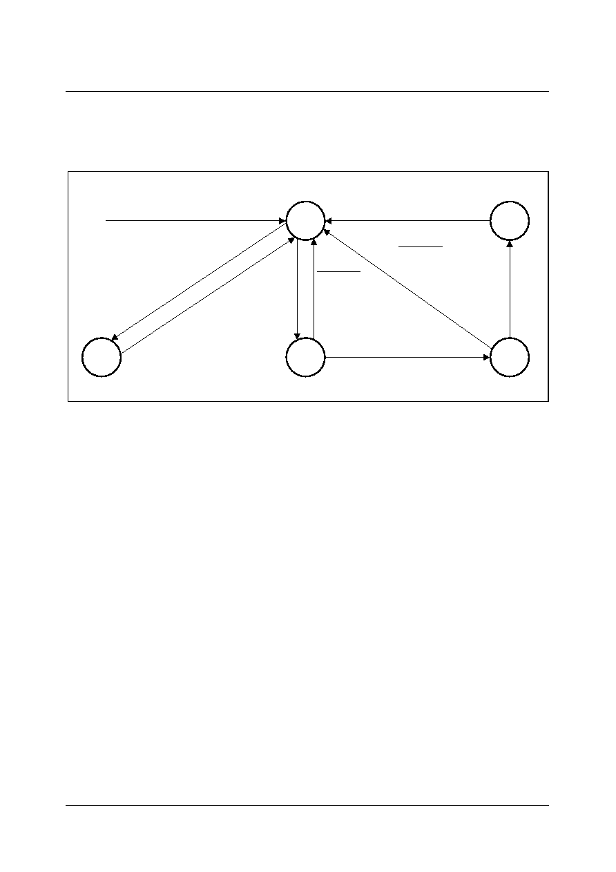
SDA 6000 / SDA 6001
PRELIMINARY DATA SHEET
Version 3.00
System Control & Configuration
6 - 12
Micronas
The following state diagram shows the state machine for security level switching and for
unlock command execution in low protected mode:
Figure 6-1
State Machine for Security Level Switching
Note:
1)
The new security level and password are valid, only if the security level
command register is accessed.
c_SCU is an abbreviation for "write access to any SCU register", i.e. write access to any
of the following registers:
SYSCON1, SYSCON2, SCUSLC, SCUSLS, RP0H, XPERCON, WDT, WDTCON,
EXICON, EXISEL, ISNC, FOCON, SYSCON3
Note: The FOCON and SYSCON3 registers do not provide any function within the M2.
Nevertheless they are implemented in the system control unit of the embedded
microcontroller and write access to the associated addresses will influence the
state machine for security level switching.
Write Access in Low Protected Mode
The write access in low protected mode is also done via a command sequence. First the
specific command 4 (see Figure 6-1) has to be written to register SCUSLC with the
current password. After this command, all security registers are unlocked until the next
write access to any SCU register is done. Read access is always possible to all registers
of the SCU and will not influence the command sequences. In register SCUSCS the
actual status of the command state machine can always be read.
It is recommended to use an atomic sequence for all command sequences.
UED11131
State 0
State 1
State 4
Command 0
Command 1
or any other SCU
Register Write Access
State 2
State 3
Command 2
Register Write Access
or any other SCU
Command 2
Register Write Access
or any other SCU
Command 3
1)
Command 1
and Low Protected Mode
Command 4
Any SCU
Register Write Access
Reset
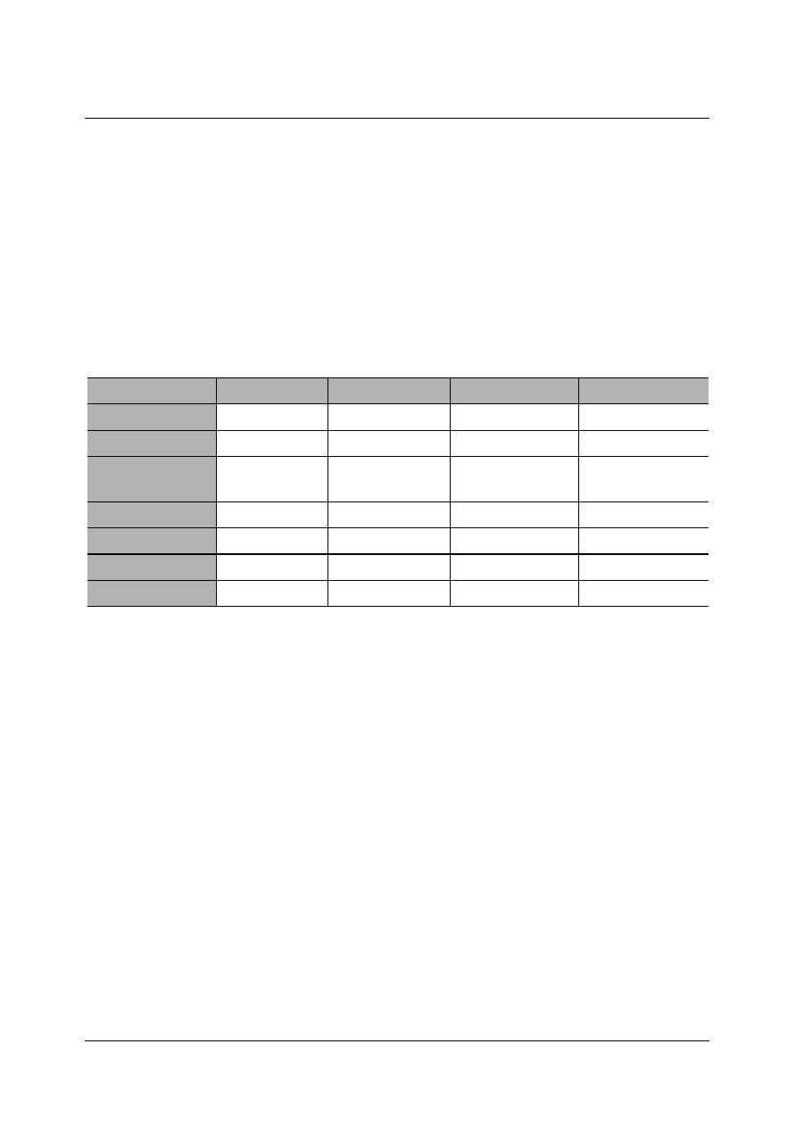
SDA 6000 / SDA 6001
PRELIMINARY DATA SHEET
Version 3.00
System Control & Configuration
6 - 13
Micronas
6.4
Power Reduction Modes
Three power reduction modes with different levels of power reduction, which may be
entered under software control, have been implemented in M2:
Idle Mode: The CPU is stopped, while the peripherals including watchdog timer continue
their operation at low clock frequency.
Sleep Mode: CPU, peripherals and PLL are completely turned off. The controller ADC
operates in wake-up mode. The real-time-clock is still in operation.
Power Down Mode: All modules are turned off.
In the table above clocking frequencies have been specified, indicating that power
reduction is achieved by means of clock-gating. None of the power supplies are
internally switched, neither may voltage be turned off at the supply pins.
M2's power management functions are supplemented by a Real Time Clock (RTC) timer
with optional periodic wake-up from idle mode. The periodic wake-up combines the
reduced power consumption in power reduction modes with a high level of system
availability. External signals and events can be scanned (at a lower rate) by periodically
activating the CPU and selected peripherals which then return to power-save mode after
a short time. This greatly reduces the system's average power consumption.
Entering and Terminating Idle and Sleep Mode
All three modes are entered by writing register SLEEPCON (see register definition
below) and issuing the IDLE instruction. All external bus actions are completed before
entry to Idle, Sleep or Power Down mode. Normal operation is resumed after Idle mode
upon any interrupt request. To return from Sleep mode, external, wake up- or RTC-
Mode
Normal
Idle
Sleep
Power Down
Oscillator
on
on
on
off
PLL
on
on
off
off
CPU
33 MHz
3 MHz/
stopped
no clock/
stopped
no clock/
stopped
CADC
33 MHz
1)
1)
Conversion mode
3 MHz
2)
2)
Wake up mode
3 MHz
2)
off
RTC
3 MHz
3 MHz
3 MHz
off
Peripherals
33 MHz
3 MHz
off
off
Bus Interface
100/66 MHz
3)
3)
Depending on value of CLKCON (see Chapter 8)
off
off
off
SDA 6000 / SDA 6001
PRELIMINARY DATA SHEET
Version 3.00
System Control & Configuration
6 - 14
Micronas
interrupt requests can be used. Power down mode can only be terminated with hardware
reset.
To prevent unintentional entry into Idle mode, the IDLE instruction has been
implemented as a protected 32-bit instruction.
Idle mode is terminated by interrupt requests from any enabled interrupt source whose
individual Interrupt Enable flag was set before the Idle mode was entered, regardless of
bit IEN.
For a request selected for CPU interrupt service, the associated interrupt service routine
is entered if the priority level of the requesting source is higher than the current CPU
priority and the interrupt system is globally enabled. After the RETI (Return from
Interrupt) instruction of the interrupt service routine is executed the CPU continues
executing the program with the instruction following the IDLE instruction. Otherwise, if
the interrupt request cannot be serviced because of a too low priority or a globally
disabled interrupt system the CPU immediately resumes normal program execution with
the instruction following the IDLE instruction.
For a request which was programmed for PEC service, a PEC data transfer is performed
if the priority level of this request is higher than the current CPU priority and the interrupt
system is globally enabled. After the PEC data transfer has been completed the CPU
remains in Idle mode. Otherwise, if the PEC request cannot be serviced because of a
too low priority or a globally disabled interrupt system, the CPU does not remain in Idle
mode but continues program execution with the instruction following the IDLE
instruction.
Mode
Idle
Sleep
Power Down
Entry by ...
writing SLEEPCON and issuing IDLE instruction
Exit by ...
any interrupt
request
external, wake up- or RTC-
IRQ
HW-reset
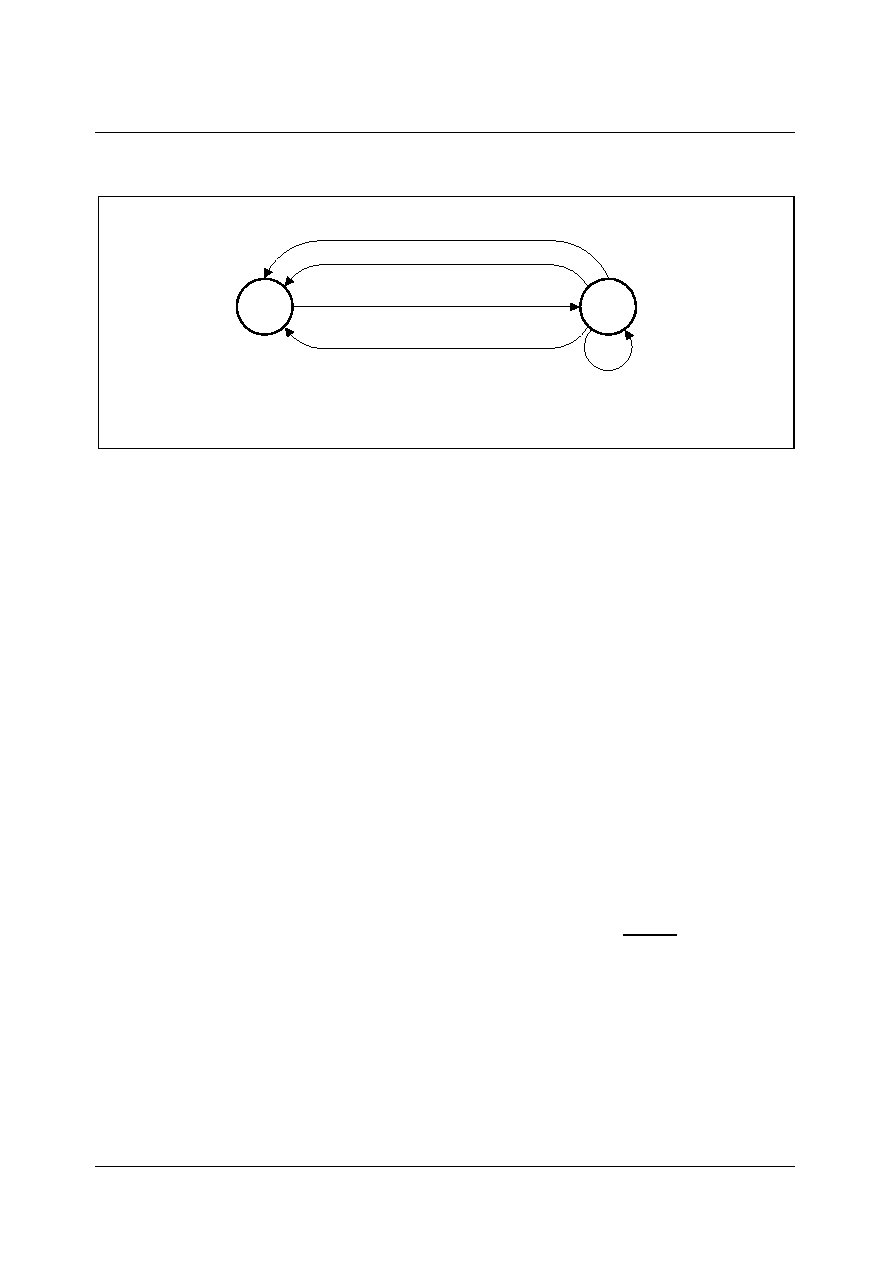
SDA 6000 / SDA 6001
PRELIMINARY DATA SHEET
Version 3.00
System Control & Configuration
6 - 15
Micronas
Figure 6-2
Transitions between Idle Mode and Active Mode
Any interrupt request, whose individual Interrupt Enable flag was set before Idle mode
was entered, will terminate Idle mode regardless of the current CPU priority. The CPU
will not go back into Idle mode when a CPU interrupt request is detected, even when the
interrupt was not serviced because of a higher CPU priority or a globally disabled
interrupt system (IEN = `0'). The CPU will only go back into Idle mode when the interrupt
system is globally enabled (IEN = `1') and a PEC service on a priority level higher than
the current CPU level is requested and executed.
Note: An interrupt request which is individually enabled and assigned to priority level 0
will terminate Idle mode. However, the associated interrupt vector will not be
accessed.
The watchdog timer may be used to monitor the Idle mode: an internal reset will be
generated if no interrupt request occurs before the watchdog timer overflows. To prevent
the watchdog timer from overflowing during Idle mode it must be programmed to a
reasonable time interval before Idle mode is entered.
Power Down Mode
Clocking of all internal blocks is stopped in Power Down Mode, the contents of the
internal RAMs, however, are preserved through the voltage supplied via the
V
DD
pins.
The watchdog timer is stopped in Power Down Mode. This mode can only be terminated
by an external hardware reset, e.g. by asserting a low level on the RSTIN pin. This reset
will initialize all SFRs and ports to their default state, but will not change the contents of
the internal RAMs.
SDRAM Refreshing
Before entering into one of the power save modes the external SDRAM must be put into
self-refresh-mode by use of register EBIDIR (see Chapter 4.5).
UED11132
Active
IDLE Instruction
Mode
Idle
Mode
Accepted
CPU Interrupt Request
Denied
Denied PEC Request
Executed
PEC Request
SDA 6000 / SDA 6001
PRELIMINARY DATA SHEET
Version 3.00
System Control & Configuration
6 - 16
Micronas
Status of Output Pins during Idle and Power Down Mode
During Idle mode the CPU is stopped, while all peripherals continue their operation in the
same way previously described. Therefore all ports pins, which are configured as
general purpose output pins, output the last data value which was written to their port
output latches. If the alternate output function of a port pin is used by a peripheral, the
state of the pin is determined by the operation of the peripheral.
Port 4 outputs the segment address for the last access on the pins that were selected
during reset, otherwise the output pins of Port 4 represent the port latch data.
During Power Down mode the oscillator and the clocks to the CPU and peripherals are
turned off. Like in idle mode, all port pins, which are configured as general purpose
output pins, output the last data value which was written to their port output latches.
When the alternate output function of a port pin is used by a peripheral the state of this
pin is determined by the last action of the peripheral before the clocks were switched off.
SYSCON1
Reset Value: 0000
H
Note: This register is a protected register; it's security level is automatically set to full
write protection after execution of the EINIT instruction.
Bit
Function
SLEEPCON Power Save Mode Selection
00: Idle
Mode
01:
Sleep Mode
10: reserved
11: Power
Down
Mode
5
4
3
2
1
0
11
10
9
8
7
6
15
14
13
12
rw
-
-
-
-
-
SLEEPCON
-
-
-
-
-
-
-
-
-

SDA 6000 / SDA 6001
PRELIMINARY DATA SHEET
Version 3.00
System Control & Configuration
6 - 17
Micronas
6.5
Dedicated Pins
M2 has different dedicated Pins than other controllers of C16X family. The following
dedicated pins are not available: ALE, READY, EA, NMI. The following table explains
M2 specific dedicated pins.
The external read strobe RD controls the output drivers of external memory or
peripherals when M2 reads data from these external devices. During reset an internal
pull-up ensures an inactive (high) level on the RD output.
The external write strobe WR controls the data transfer from the M2 to an external
memory. During reset an internal pull-up ensures an inactive (high) level on the WR
output.
Byte mask signals LDQM and UDQM control the byte access to an external SDRAM
according to the PC100 specification. These pins are active if either the high byte or the
low byte of a 16-bit word are written.
The oscillator input XTAL1 and output XTAL2 connect the internal oscillator to the
external crystal. The oscillator provides an inverter and a feedback element. An external
TTL clock signal may be fed to the input XTAL1, leaving XTAL2 open.
By using the RSTIN pin M2 can be put into the well defined reset condition either at
power-up or upon external events like a hardware failure or manual reset. The internal
reset signal can be driven on output pin RSTOUT/COR.
The chipselect signals CSDRAM
,
CSROM
,
CS3 are for general control of external
memories. During reset an internal pull-up ensures an inactive (high) level on these
outputs. CS3 can be used for a ROM.
Pin(s)
Function
RD
External Read Strobe
WR
Write Enable Strobe for SDRAM
LDQM, UDQM
Byte Mask Signals for SDRAM
XTAL1, XTAL2
Oscillator Input/Output
RSTIN
Reset Input Pin
CSDRAM
,
CSROM
,
CS3
Chip Select Signals
MEMCLK, CLKEN
Clock Signals for SDRAM
CVBS1, CVBS2
CVBS Input Signals
R, G, B
Analog RGB Output
CORBLA
Contrast Reduction and Blanking Pin
HSYNC, VSYNC
Sync Inputs/Outputs for the Display

SDA 6000 / SDA 6001
PRELIMINARY DATA SHEET
Version 3.00
System Control & Configuration
6 - 18
Micronas
Signals MEMCLK, CLKEN are used to provide a clock and an enable signal for an
external SDRAM. During reset an internal pull-down ensures an inactive (low) level on
these outputs.
CVBS1A, CVBS1B and CVBS2 can carry two analog composite video signals and act
as inputs for the two data slicers. The video signal on channel 1 can be either differential
(CVBS1A and CVBS1B) or single-ended (CVBS1A, CVBS1B to ground).
R, G, B are analog outputs from the display generator.
CORBLA is a signal which indicates whether a pixel created by M2 should be displayed
or mixed with external video source (blanking function). At the same time this signal
carries information on contrast reduction of this pixel. Alternatively BLANK can be
generated as a separate output signal. COR can be generated separately as well, in
which case no RSTOUT is available.
HSYNC and VSYNC are bidirectional pins which are used to synchronize M2 to an
external video source or to deliver a stable horizontal and vertical sync timing to external
components.

SDA 6000 / SDA 6001
PRELIMINARY DATA SHEET
Version 3.00
System Control & Configuration
6 - 19
Micronas
6.6
XBUS Configuration
Although the XBUS is not visible at the chip boundary, some registers have to be set to
guarantee correct operation. The user has to program the XBUS-registers in the
following way:
Register
Value
SYSCON
E444
H
XADRS1
0E03
H
XADRS2
0E83
H
XADRS3 - XADRS6 (not used)
0000
H
ADDRSEL1 - ADDRSEL4 (not used)
0000
H
XBCON1
05BF
H
XBCON2
05BF
H
XBCON3 - XBCON6 (not used)
0000
H
BUSCON0
15B7
H
BUSCON1 - BUSCON4 (not used)
0000
H
XPERCON
0003
H
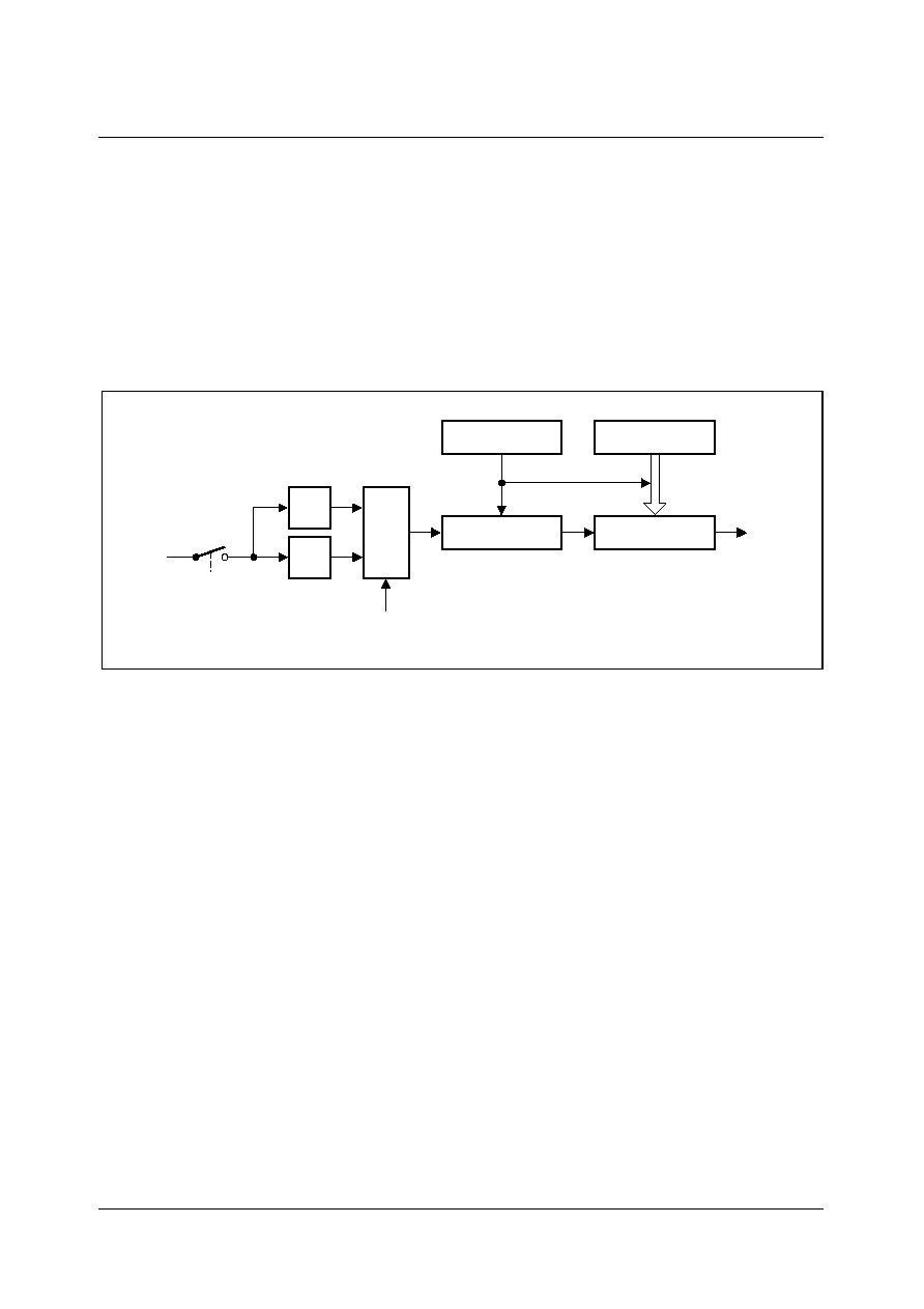
SDA 6000 / SDA 6001
PRELIMINARY DATA SHEET
Version 3.00
System Control & Configuration
6 - 20
Micronas
6.7
Watchdog Timer
The watchdog timer is a 16-bit up counter which can be clocked with the CPU clock
(
f
CPU
), either divided by 2 or divided by 128. This 16-bit timer is realized as two
concatenated 8-bit timers (see Figure 6-3). The upper 8 bits of the watchdog timer can
be preset to a user-programmable value via a watchdog service access in order to vary
the watchdog expire time. The lower 8 bits are reset on each service access.
The following figure shows the WDT block diagram:
Figure 6-3
WDT Block Diagram
The current count value of the Watchdog Timer is contained in the Watchdog Timer
Register WDT, which is a non-bitaddressable read-only register. The operation of the
Watchdog Timer is controlled by its bitaddressable Watchdog Timer Control Register
WDTCON. This register specifies the reload value for the high byte of the timer and
selects the input clock prescaling factor.
After any software reset, external hardware reset (see note), or watchdog timer reset,
the watchdog timer is enabled and starts counting up from 0000
H
with the frequency
f
CPU
/2. The input frequency may be switched to
f
CPU
/128 by setting bit WDTIN. The
watchdog timer can be disabled via the instruction DISWDT (Disable Watchdog Timer).
Instruction DISWDT is a protected 32-bit instruction which will ONLY be executed during
the time between a reset and execution of either the EINIT (End of Initialization) or the
SRVWDT (Service Watchdog Timer) instruction. Either one of these instructions
disables the execution of DISWDT.
When the watchdog timer is not disabled via instruction DISWDT it will continue counting
up, even during Idle Mode. If it is not serviced by the SRVWDT instruction by the time
the count reaches FFFF
H
the watchdog timer will overflow and cause an internal reset.
In this case the Watchdog Timer Reset Indication Flag (WDTR) in register WDTCON will
be set.
UEB11133
WDT Control
WDT Low Byte
WDT
f
MUX
WDTIN
DISWDT
Clear
WDT High Byte
WDTREL
WDTR
2
�
128
�
SDA 6000 / SDA 6001
PRELIMINARY DATA SHEET
Version 3.00
System Control & Configuration
6 - 21
Micronas
To prevent the watchdog timer from overflowing, it must be serviced periodically by the
user software. The watchdog timer is serviced with the instruction SRVWDT, which is a
protected 32-bit instruction. Servicing the watchdog timer clears the low byte and reloads
the high byte of the watchdog time WDT register with the preset value in bit field
WDTREL, which is the high byte of the WDTCON register. Servicing the watchdog timer
will also reset the WDTR bit. After being serviced the watchdog timer continues counting
up from the value (<WDTREL>
�
28). Instruction SRVWDT has been encoded in such a
way that the chance of unintentionally servicing the watchdog timer (e.g. by fetching and
executing a bit pattern from a wrong location) is minimized. When instruction SRVWDT
does not match the format for protected instructions, the Protection Fault Trap will be
entered, rather than the instruction being executed.
The time period for an overflow of the watchdog timer is programmable in two ways:
� The input frequency of the watchdog timer can be selected via bit WDTIN in register
WDTCON
to be either
f
CPU
/2 or
f
CPU
/128.
� The reload value WDTREL for the high byte of WDT can be programmed in register
WDTCON.
The period P
WDT
between servicing the watchdog timer and the next overflow can
therefore be determined by the following formula:
P
WDT
= (2
(1 + <WDTIN>
�
6)
�
(2
16
� <WDTREL>
�
2
8
))/
f
CPU
[1]
Table 6-1 marks the possible ranges for the watchdog time which can be achieved using
a certain CPU clock. Some numbers are rounded to 3 significant digits.
Note: For safety reasons, the user is advised to rewrite WDTCON each time before the
watchdog timer is serviced.
Here is the description of the Watchdog timer SFRs.
Table 6-1
Watchdog Time Ranges
Reload Value
in WDTREL
Prescaler for
f
CPU
2 (WDTIN = `0')
128 (WDTIN = `1')
33.33 MHz
3 MHz
33.33 MHz
3 MHz
FF
H
0.0
�
s
0.0
�
s
0.0 ms
0.0 ms
7F
H
2.0 ms
22.0 ms
126.8 ms
1.41 s
00
H
3.9 ms
43.7 ms
251.7 ms
2.79 s
SDA 6000 / SDA 6001
PRELIMINARY DATA SHEET
Version 3.00
System Control & Configuration
6 - 22
Micronas
WDTCON
Reset Value: 00XX
H
Note: The reset value depends on the reset source (see description below).
The execution of EINIT clears the reset indication flags.
Note: When the reset output is enabled pin RSTOUT will be pulled low for the duration
of the internal reset sequence upon a watchdog timer reset.
WDT Timer Register
The WDT register contains the current count value of the Watchdog Timer.
WDT
Reset Value: 0000
H
Note: This register in a read-only register. Write access can be performed to this
register, during test mode only.
Bit
Function
WDTIN
Watchdog Timer Input Frequency Selection
0: Input
frequency
is
f
CPU
/2
1: Input
frequency
is
f
CPU
/128
WDTR
Watchdog Timer Reset Indication Flag
Cleared by a hardware reset or by the SRVWDT instruction.
SWR
Software Reset Indication Flag
SHWR
Short Hardware Reset Indication Flag
LHWR
Long Hardware Reset Indication Flag
WDTREL
(7 ... 0)
Watchdog Timer Reload Value
(for the high byte of WDT)
5
4
3
2
1
0
11
10
9
8
7
6
15
14
13
12
rw
r
r
r
r
rw
WDTREL(7 .. 0)
-
-
-
LHW
R
SHW
R
SW
R
WDT
R
WDT
IN
5
4
3
2
1
0
11
10
9
8
7
6
15
14
13
12
r
WDT(15 .. 0)
SDA 6000 / SDA 6001
PRELIMINARY DATA SHEET
Version 3.00
System Control & Configuration
6 - 23
Micronas
Reset Source Indication
The reset indication flags in register WDTCON provide information on the source of the
last reset. As M2 starts executing from location 00'0000
H
after any possible reset event,
the initialization software may check these flags in order to determine if the recent reset
event was triggered by an external hardware signal (via RSTIN), by software itself or by
an overflow of the watchdog timer. The initialization (and also the further operation) of
the microcontroller system can thus be adapted to the respective circumstances, e.g. a
special routine may verify the software integrity after a watchdog timer reset.
The reset indication flags are not mutually exclusive, e.g. more than one flag may be set
after reset depending on its source. The table below summarizes the possible
combinations:
Note: *) When the reset output is enabled, the indicated flags are also set in the
respective reset case. The WDTCON reset value will then be different from the
table value.
Note: The listed reset values for WDTCON assume the reserved bits as `0'.
Long Hardware Reset is indicated when the RSTIN input is still sampled low (active) at
the end of a hardware triggered internal reset sequence.
Short Hardware Reset is indicated when the RSTIN input is sampled high (inactive) at
the end of a hardware triggered internal reset sequence.
Software Reset is indicated after a reset triggered by the execution of instruction SRST.
Watchdog Timer Reset is indicated after a reset triggered by an overflow of the
watchdog timer.
Note: When reset output is enabled the RSTOUT pin is pulled low for the duration of the
internal reset sequence upon any sort of reset.
Therefore a long hardware reset (LHWR) will be recognized in any case.
Table 6-2
Reset Indication Flag Combinations
Reset Indication Flags
Reset Source
LHWR
SHWR
SWR
WDTR
Long Hardware Reset
X
X
X
�
Short Hardware Reset
*
X
X
�
Software Reset
*
*
X
�
Watchdog Timer Reset
*
*
X
X
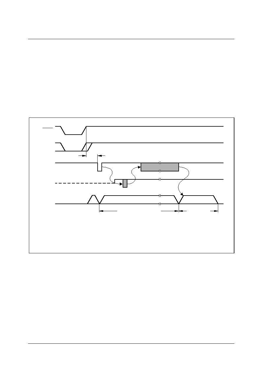
SDA 6000 / SDA 6001
PRELIMINARY DATA SHEET
Version 3.00
System Control & Configuration
6 - 24
Micronas
6.8
Bootstrap Loader
The bootstrap loader of M2 works in the same way as implemented in other C16x
derivatives. It provides a mechanism to load the start-up program, which is executed
after reset, via a serial interface (ASC). In this case no external (ROM) memory is
required.
The bootstrap loader moves code/data into the internal RAM, but it is also possible to
transfer data via the serial interface into an external RAM using a second level loader
routine.
Figure 6-4
Bootstrap Loader Sequence
The M2 enters BSL mode, if pin P4.0 is sampled low at the end of a hardware reset.
When M2 has entered BSL mode, the following configuration is automatically set (values
that deviate from the normal reset values, are marked):
Watchdog Timer:
Disabled
Register SYSCON:
0C00
H
Context Pointer CP:
FA00
H
Register STKUN:
FA40
H
Stack Pointer SP:
FA40
H
Register STKOV:
FA0C
H
0 <-> C
Register S0CON:
8001
H
UET11134
RSTIN
P4.0
RxD0
TxD0
CSP:IP
1)
2)
4)
3)
Int. Boot ROM BSL-routine
32 bytes
User Software
BSL initialization time, > 1.5
1)
�
s @
CPU
f
= 33 MHz
Zero byte (1 start bit, eight '0' data bits, 1 stop bit), sent by host
2)
3)
Identification byte (D5
H
) sent by M2
4)
32 bytes of code/data, sent by host

SDA 6000 / SDA 6001
PRELIMINARY DATA SHEET
Version 3.00
System Control & Configuration
6 - 25
Micronas
Register BUSCON0: according to start-up config.
Register S0BG:
according to `00' byte
P3.10/TXD0:
`1'
DP3.10:
`1'
Other than after a normal reset the watchdog timer is disabled, therefore the bootstrap
loading sequence is not time limited. Pin TXD0 is configured as output. The configuration
(e.g. the accessibility) of the M2's memory areas after reset in Bootstrap-Loader mode
differs from the standard case. Accesses to the external ROM area are partly redirected,
while the M2 is in BSL mode. All code fetches to segment 0 are made from the special
Boot-ROM, while data accesses read from the external user ROM.
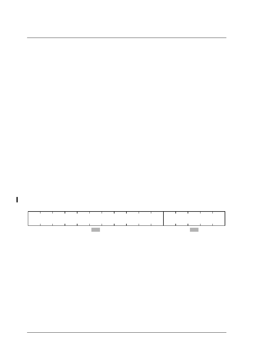
SDA 6000 / SDA 6001
PRELIMINARY DATA SHEET
Version 3.00
System Control & Configuration
6 - 26
Micronas
6.9
Identification Registers
A set of 8 identification registers are provided to offer information on the chip as
manufacturer, chip type and its memory (EEPROM, OTP, DRAM or Flash memory)
properties, and information on the CSCU (type of module, redesign state).
The ID registers are read only registers. These registers are:
� IDMANUF, for manufacturer and department identification,
� IDCHIP, for device identification and revision code,
� IDMEM, for identification of on-chip program memory (type, size),
� IDMEM2, for identification of additional EEPROM, OTP, DRAM or Flash memory,
� IDPROG, for identification of programming/erasing voltage of on-chip program
memory,
� IDRT, redesign tracking register for identification of revisions and laser cuts.
Besides, some other registers provide identification of some parts of the M2. These
registers are hardwired inside the M2.
� CPUID, for CPU identification,
� IDSCU, for CSCU identification,
� DIPX version bit field, for OCDS identification.
6.9.1
System Identification
These identific ID register description
IDMANUF
Reset Value: 1828
H
5
4
3
2
1
0
11
10
9
8
7
6
15
14
13
12
r
r
MANUF
DEPT

SDA 6000 / SDA 6001
PRELIMINARY DATA SHEET
Version 3.00
System Control & Configuration
6 - 27
Micronas
IDCHIP Reset Value: 0003
H
(SDA6000) / 0007
H
(SDA6001)
IDMEM
Reset Value: XXXX
H
IDMEM2
Reset Value: XXXX
H
Note: IDMEM2 describes the second block of (program) memory. E.g. a device may
contain Flash and EEPROM or DRAM sections. Static RAM modules are not
described with ID registers.
Bit
Function
MANUF
Manufacturer
This is the JEDEC normalized manufacturer code.
0C1
H
:Infineon Technologies
020
H
: SGS-Thomson
DEPT
Department
Indicates the department within Micronas and Infineon Technologies.
00
H
: HL MC
01
H
: HL CAD Macrocells
02
H
: HL IT
Bit
Function
Revision
Device Revision Code
Identifies the device step where the first release is marked `01
H
'.
CHIPID
Device Identification
Identifies the device name. Please refer to the association table.
5
4
3
2
1
0
11
10
9
8
7
6
15
14
13
12
r
r
CHIPID
Chip Revision Number
5
4
3
2
1
0
11
10
9
8
7
6
15
14
13
12
r
r
Type
Size
5
4
3
2
1
0
11
10
9
8
7
6
15
14
13
12
r
r
Type
Size

SDA 6000 / SDA 6001
PRELIMINARY DATA SHEET
Version 3.00
System Control & Configuration
6 - 28
Micronas
IDPROG
Reset Value: XXXX
H
Note:
1)
Devices that incorporate memories which cannot be programmed outside the
factory will indicate `00
H
' in both bit fields.
IDRT
Reset Value: XXXX
H
Note: The Redesign Tracing register IDRT is not commonly specified. It is protected
against standard read accesses via the function testmode (Testmode A).
Bit
Function
Size
Size of On-chip Program Memory
The size of the implemented program memory in terms of 4 K blocks, i.e.
Memory-size = <Size>
�
4 KByte.
Type
Type of On-chip Program Memory
Identifies the memory type on this silicon.
0
H
: ROMless
1
H
: Mask ROM
2
H
: EPROM
3
H
: Flash
4
H
: OTP
5
H
: EEPROM
6
H
: DRAM/SRAM
Bit
Function
PROGVDD
Programming
V
DD
Voltage
1)
The voltage of the standard power supply pins required when
programming or erasing (if applicable) the on-chip program memory.
Formula:
V
DD
= 20
�
<PROGVDD>/256 [V]
PROGVPP
Programming
V
PP
Voltage
1)
The voltage of the special programming power supply (if existent)
required to program or erase (if applicable) the on-chip program
memory. Formula:
V
PP
= 20
�
<PROGVPP>/256 [V]
5
4
3
2
1
0
11
10
9
8
7
6
15
14
13
12
r
r
PROGVPP
PROGVDD
-
RA
-
-
-
-
-
-
-
-
-
-
-
LC
5
4
3
2
1
0
11
10
9
8
7
6
15
14
13
12
r
r
RIX
r
-
-
-
-
-
-
-
-
-
-
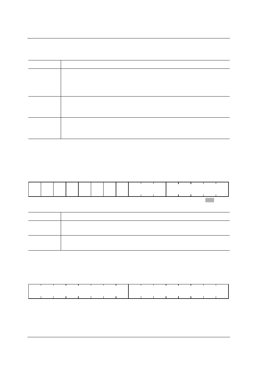
SDA 6000 / SDA 6001
PRELIMINARY DATA SHEET
Version 3.00
System Control & Configuration
6 - 29
Micronas
6.9.2
CPU Identification
The CPU is identified by the CPUID register. This register is only implemented on
STARLIB versions of the M2 Rev. 2.0.
CPUID
Reset Value: 0061
H
The SCU provides a specific read-only identification register for its own module type and
revision identification.
IDSCU
Reset Value: 0000
H
For Rev. 2.0 derivatives, the current value is 0000
H
.
Bit
Function
RIX
Redesign Index
0:
This device is the original "Revision".
else: This device has experienced minor changes that are not reflected
to the customer by the "Revision" bit field.
RA
Redundancy Activation
0:
This device is as it was manufactured.
1:
Redundant memory structures have been activated.
LC
Laser Correction
0:
This device is as it was manufactured.
1:
This device has been laser corrected.
Bit
Function
CBC Rev.
CBC Revision number
currently 011
B
Core ID
Core Identification number
for the C166 CBC the value is 00001
B
-
-
-
-
-
-
-
-
-
5
4
3
2
1
0
11
10
9
8
7
6
15
14
13
12
r
Core ID
-
-
-
-
-
-
-
-
-
-
CBC Rev.
5
4
3
2
1
0
11
10
9
8
7
6
15
14
13
12
r
SCU Module Number
r
SCU Revision Number
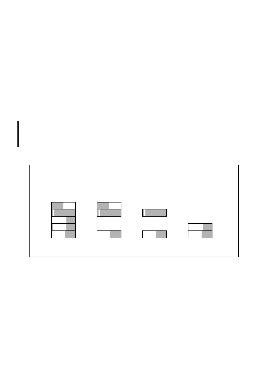
SDA 6000 / SDA 6001
PRELIMINARY DATA SHEET
Version 3.00
System Control & Configuration
6 - 30
Micronas
6.10
Parallel Ports
M2 provides up to 30 input/outputs, 6 output and 6 input multiple purpose ports. All port
lines are bit-addressable, and all input/output lines are individually (bit-wise)
programmable as inputs or outputs via direction registers. The I/O ports are true
bidirectional ports which are switched to high impedance state when configured as
inputs. The output drivers of two I/O ports can be configured (pin by pin) for push/pull
operation or open-drain operation via control registers. During the internal reset, all port
pins are configured as inputs. Most of the port lines have programmable alternate input
or output functions associated with them (GPT1/GPT2, external interrupts, I
2
C-bus,
analog inputs for A/D converter, SSC-interface or ASC-interface). Some ports also have
a third functionality next to the functions described inside this chapter. This third
functionality is used for digital RGB interfacing and disabled after reset. For further
information on this third function please refer to Chapter 10.8. All port lines that are not
used for these alternate functions may be used as general purpose I/O lines. Ports of M2
are 3.3 V tolerant and can deliver a 3.3 V output voltage (refer also to Chapter 14).
Figure 6-5
Portlogic Register Overview
Port 0
Port 0 does not exist due to the dedicated memory bus structure of M2.
Port 1
Port 1 does not exist due to the dedicated memory bus structure of M2.
Port 2
Port 2 is an 8-bit bidirectional I/O port which can also serve as fast external interrupt input
(sample rate is 30 ns).
UEA11135
Registers
P2
P3
P4
P5
P6
Data Input/ Output
Open Drain Control
Registers
Direction Control
Registers
DP6
DP2
DP3
ODP6
ODP3
ALTSELOP6
P5BEN
Registers
Special Control

SDA 6000 / SDA 6001
PRELIMINARY DATA SHEET
Version 3.00
System Control & Configuration
6 - 31
Micronas
P2
Reset Value: 0000
H
DP2
Reset Value: 0000
H
Bit
Function
P2.y
Port data register P2 bit y.
Bit
Function
DP2.y
Port direction register DP2 bit y
DP2.y = 0: Port line P2.y is an input (high-impedance).
DP2.y = 1: Port line P2.y is an output.
5
4
3
2
1
0
11
10
9
8
7
6
15
14
13
12
rw
rw
rw
rw
rw
rw
rw
rw
P2.15 P2.14 P2.13 P2.12 P2.11 P2.10
P2.9
P2.8
-
-
-
-
-
-
-
-
5
4
3
2
1
0
11
10
9
8
7
6
15
14
13
12
rw
rw
rw
rw
rw
rw
rw
rw
DP2.
15
DP2.
14
DP2.
13
DP2.
12
DP2.
11
DP2.
10
DP2.
9
DP2.
8
-
-
-
-
-
-
-
-
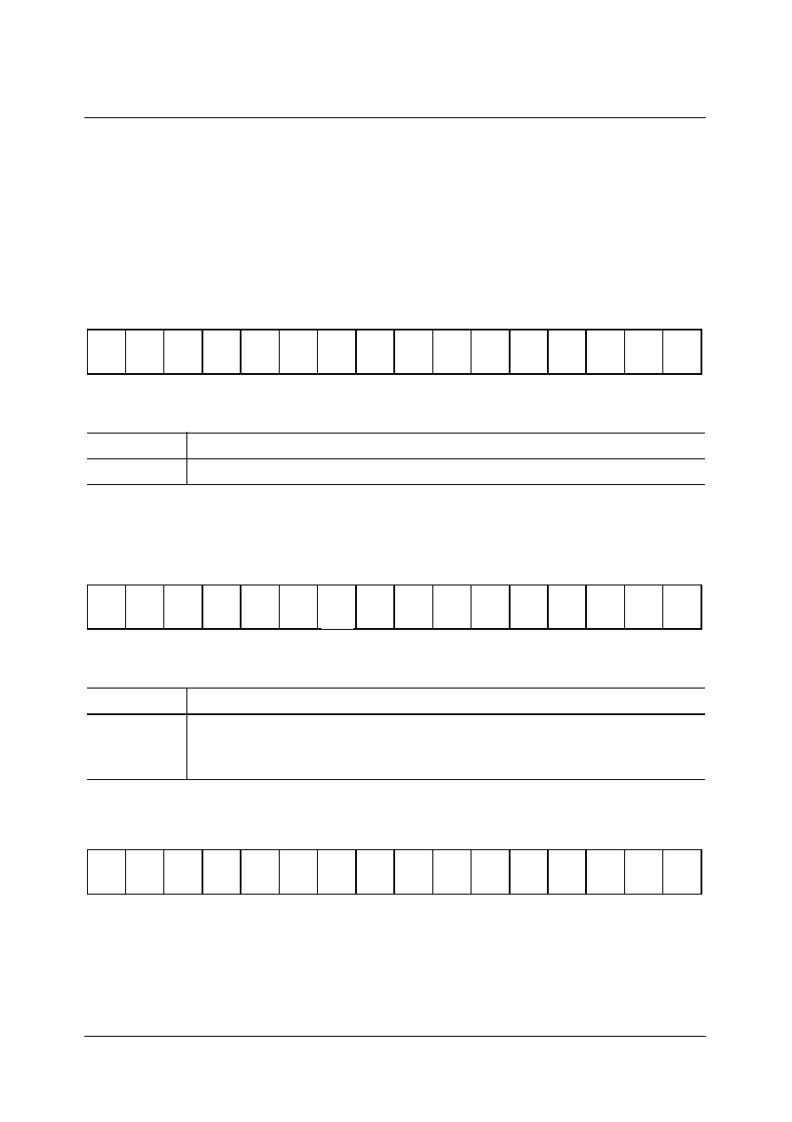
SDA 6000 / SDA 6001
PRELIMINARY DATA SHEET
Version 3.00
System Control & Configuration
6 - 32
Micronas
Port 3
If this 15-bit port is used for general purpose I/O, the direction of each line can be
configured via the corresponding direction register DP3. All port lines can be switched
into push/pull or open drain mode via the open drain control register ODP3. Due to pin
limitations register bit P3.14 is not connected to any pin.
P3
Reset Value: 0000
H
Note: Register bit P3.14 is not connected to an I/O pin.
DP3
Reset Value: 0000
H
ODP3
Reset Value: 0000
H
Bit
Function
P3.y
Port data register P3 bit y.
Bit
Function
DP3.y
Port direction register DP3 bit y
DP3.y = 0: Port line P3.y is an input (high-impedance).
DP3.y = 1: Port line P3.y is an output.
5
4
3
2
1
0
11
10
9
8
7
6
15
14
13
12
rw
rw
rw
rw
rw
rw
rw
rw
rw
rw
rw
rw
rw
rw
rw
P3.15
-
P3.13 P3.12 P3.11 P3.10
P3.9
P3.8
P3.7
P3.6
P3.5
P3.4
P3.3
P3.2
P3.1
P3.0
5
4
3
2
1
0
11
10
9
8
7
6
15
14
13
12
rw
-
rw
rw
rw
rw
rw
rw
rw
rw
rw
rw
rw
rw
rw
rw
DP3.
15
-
DP3.
13
DP3.
12
DP3.
11
DP3.
10
DP3.
9
DP3.
8
DP3.
7
DP3.
6
DP3.
5
DP3.
4
DP3.
3
DP3.
2
DP3.
1
DP3.
0
5
4
3
2
1
0
11
10
9
8
7
6
15
14
13
12
rw
rw
rw
rw
rw
rw
rw
rw
rw
rw
rw
rw
rw
rw
rw
ODP3.
15
-
ODP3.
13
ODP3.
12
ODP3.
11
ODP3.
10
ODP3.
9
ODP3.
8
ODP3.
7
ODP3.
6
ODP3.
5
ODP3.
4
ODP3.
3
ODP3.
2
ODP3.
1
ODP3.
0
-

SDA 6000 / SDA 6001
PRELIMINARY DATA SHEET
Version 3.00
System Control & Configuration
6 - 33
Micronas
Alternate Functions of Port 3
The pins of Port 3 serve various functions which include external timer control lines and
the 3 serial interfaces.
The table below summarizes the alternate functions of Port 3.
Port 4
Port 4 is a 6-bit output port. Because of its high frequency requirements in the alternate
function mode, it has different electrical characteristics than the other ports.
During reset, the user specific portion of the system start-up configuration is input via
Port 4. The complete configuration (user specific as well as hardwired settings) can be
read at runtime from register RP0H. For a detailed description refer to Chapter 6.1.
Bit
Function
ODP3.y
Port 3 Open Drain control register bit y
ODP3.y = 0: Port line P3.y output driver in push/pull mode.
ODP3.y = 1: Port line P3.y output driver in open drain mode.
Port 3 Pin Alternate Function
P3.0
P3.1
P3.2
P3.3
P3.4
P3.5
P3.6
P3.7
P3.8
P3.9
P3.10
P3.11
P3.12
P3.13
P3.14
P3.15
SCL0
I
2
C - bus clock line 0
SDA0
I
2
C - bus data line 0
CAPIN
GPT2 capture input
T3OUT
Timer 3 Toggle output
T3EUD
Timer 3 External Up/Down input
T4IN
Timer 4 Count input
T3IN
Timer 3 Count input
T2IN
Timer 2 Count input
MRST
SSC Master receive/Slave transmit
MTSR
SSC Master transmit/Slave receive
TxD0
ASC0 Transmit data output
RxD0
ASC0 Receive data input
---
No alternate function
SCLK
SSC Shift Clock input/output
---
Not implemented. No pin assigned!
LED2
No alternate function
SDA 6000 / SDA 6001
PRELIMINARY DATA SHEET
Version 3.00
System Control & Configuration
6 - 34
Micronas
P4L (during reset)
Reset Value: XXXX
H
P4
Reset Value: 0000
H
Alternate Functions of Port 4
During external bus cycles that use segmentation (e.g. an address space above
128 KByte), a number of Port 4 pins may output the segment address lines and activate
the third chip select signal (A(20 ... 16) and CS3). The number of pins that is used for
segment address output determines the external address space which is directly
accessible. The other pins of Port 4 (if any) may be used for general purpose output. If
segment address lines are selected, the alternate function of Port 4 may be necessary
to access e.g. external memory directly after reset. For this reason Port 4 will be
automatically switched to this alternate function.
Bit
Function
P4L.0
BSLENA (Boot Strap Load Enable)
P4L.0 = 1: Boot strap loader enabled
P4L.0 = 0: Boot strap loader disabled
P4L.1
CSENA (Chip Select Enable)
P4L.1 = 1: P4.5 configured as general purpose pin
P4L.1 = 0: P4.5 configured as CS3
P4L.2
Reserved
P4L.(5 ... 3)
SALSEL(2 ... 0) (Select Number of Address Lines)
see explanation below
Bit
Function
P4.y
Port data register P4 bit.y
5
4
3
2
1
0
11
10
9
8
7
6
15
14
13
12
-
-
-
-
-
-
-
-
-
-
P4L.5 P4L.4 P4L.3 P4L.2 P4L.1 P4L.0
r
r
r
r
r
r
5
4
3
2
1
0
11
10
9
8
7
6
15
14
13
12
rw
rw
rw
rw
rw
rw
-
-
-
-
-
-
-
-
-
-
P4.5
P4.4
P4.3
P4.2
P4.1
P4.0
SDA 6000 / SDA 6001
PRELIMINARY DATA SHEET
Version 3.00
System Control & Configuration
6 - 35
Micronas
The number of segment address lines is selected via P4 during reset. The selected value
can be read from bit field SALSEL and CSENA of register RP0H e.g. in order to check
the configuration during run time.
Port 5
Port 5 is a 6-bit input port.
P5
Reset Value: 0000
H
Alternate Functions of Port 5
Port 5.3 ... P5.0 is also connected to the input multiplexer of the A/D Converter. These
lines can accept analog signals (AN3 ... AN0) that can be converted by the ADC. Port
5.15 and 5.14 also serve as external timer control lines for GPT1 and GPT2.
Port 4
Pin
Altern.
Function
SALSEL = 111
Altern.
Function
SALSEL = 110
Altern.
Function
SALSEL = 101
Altern.
Function
SALSEL = 100
Altern.
Function
SALSEL = 011
SALSEL = 010 or
001 or 000
P4.0
A16
A16
A16
A16
A16
Gen. Purp. I/O
P4.1
A17
A17
A17
A17
Gen. Purp. I/O Gen. Purp. I/O
P4.2
A18
A18
A18
Gen. Purp. I/O Gen. Purp. I/O Gen. Purp. I/O
P4.3
A19
A19
Gen. Purp. I/O Gen. Purp. I/O Gen. Purp. I/O Gen. Purp. I/O
P4.4
A20
Gen. Purp. I/O Gen. Purp. I/O Gen. Purp. I/O Gen. Purp. I/O Gen. Purp. I/O
Port 4 Pin
Altern. Function
CSENA = 0
Altern. Function
CSENA = 1
P4.5
CS3
Gen. Purp. I/O
Bit
Function
P5.y
Port data register P5 bit y (read only).
5
4
3
2
1
0
11
10
9
8
7
6
15
14
13
12
r
r
r
r
r
r
P5.15 P5.14
-
-
-
-
-
-
-
-
-
-
P5.3
P5.2
P5.1
P5.0
SDA 6000 / SDA 6001
PRELIMINARY DATA SHEET
Version 3.00
System Control & Configuration
6 - 36
Micronas
P5BEN
Reset Value: 0000
H
Port 6
If this 7-bit port is used for general purpose I/O, the direction of each line can be
configured via the corresponding direction register DP6. The port lines can be switched
into push/pull or open drain mode via the open drain control register ODP6.
P6
Reset Value: 0000
H
Port 5 Pin Alternate Function
P5.0
P5.1
P5.2
P5.3
P5.14
P5.15
ANA0Analog Input 0 (Wake Up Function)
ANA1Analog Input 1
ANA2Analog Input 2
ANA3 Analog Input 3
T4EUDTimer 4 External Up/Down Input
T2EUDTimer 2 External Up/Down Input
Bit
Function
P5BEN.y
Input Functionality Control Bit
P5BEN.y = 0: Analog Input Functionality.
P5BEN.y = 1: Digital Input Functionality.
Bit
Function
P6.y
Port data register P6 bit y.
5
4
3
2
1
0
11
10
9
8
7
6
15
14
13
12
-
-
-
-
-
-
-
-
-
-
-
-
P5B
EN.3
P5B
EN.2
P5B
EN.1
P5B
EN.0
rw
rw
rw
rw
5
4
3
2
1
0
11
10
9
8
7
6
15
14
13
12
rw
rw
rw
rw
rw
rw
rw
-
-
-
-
-
-
-
-
-
P6.6
P6.5
P6.4
P6.3
P6.2
P6.1
P6.0

SDA 6000 / SDA 6001
PRELIMINARY DATA SHEET
Version 3.00
System Control & Configuration
6 - 37
Micronas
DP6
Reset Value: 0000
H
ODP6
Reset Value: 0000
H
Alternate Functions of Port 6
The table below summarizes the alternate functions of Port 6.
Bit
Function
DP6.y
Port direction register DP6 bit y.
DP6.y = 0: Port line P6.y is an input (high-impedance).
DP6.y = 1: Port line P6.y is an output.
Bit
Function
ODP6.y
Port 6 Open Drain control register bit y
ODP6.y = 0: Port line P6.y output driver in push/pull mode
ODP6.y = 1: Port line P6.y output driver in open drain mode
Port 6 Pin Alternate Function
P6.0
P6.1
P6.2
P6.3
P6.4
P6.5
P6.6
TRIG_IN
Trigger Input for Emulation
TRIG_OUT
Trigger output for Emulation
FIELD
Field signal from field detection of OSD
SCL1
I
2
C Bus Clock Line 1
SDA1
I
2
C Bus Data Line 1
no alternate function
SDA2
I
2
C Bus Data Line 2
5
4
3
2
1
0
11
10
9
8
7
6
15
14
13
12
rw
rw
rw
rw
rw
rw
rw
-
-
-
-
-
-
-
-
-
DP6.6 DP6.5 DP6.4 DP6.3 DP6.2 DP6.1 DP6.0
5
4
3
2
1
0
11
10
9
8
7
6
15
14
13
12
rw
rw
rw
rw
rw
rw
rw
-
-
-
-
-
-
-
-
-
ODP6.
6
ODP6.
5
ODP6.
4
ODP6.
3
ODP6.
2
ODP6.
1
ODP6.
0

SDA 6000 / SDA 6001
PRELIMINARY DATA SHEET
Version 3.00
System Control & Configuration
6 - 38
Micronas
ALTSEL0P6
Reset Value: 0000
H
Bit
Function
SELP6.y
Alternate Function Control Bit
SELP6.y = 0: General Purpose Port Functionality enabled for Line P6.y.
SELP6.y = 1: Alternate Function enabled for Line P6.y.
5
4
3
2
1
0
11
10
9
8
7
6
15
14
13
12
rw
rw
rw
rw
rw
rw
rw
-
-
-
-
-
-
-
-
-
SEL
P6.6
SEL
P6.5
SEL
P6.4
SEL
P6.3
SEL
P6.2
SEL
P6.1
SEL
P6.0

SDA 6000 / SDA 6001
PRELIMINARY DATA SHEET
Version 3.00
System Control & Configuration
6 - 39
Micronas
6.11
On board FLASH/EPROM-programming
All bidirectional pins of M2 can be switched to input state and some output pins to high
impedant state, by generating external signal patterns which are then applied to four
dedicated pins (TMODE, TMS, TCK, TDI). For three of those pins (TMS, TCK, TDI) a
first signal pattern is applied. A rising edge at TMODE indicates that the pattern is stable
and to latch the pattern SDA6000 internally. Afterwards a second pattern needs to be
forced to TMS, TCK and TDI. This second pattern is the inverted first pattern. Again a
second rising edge at TMODE indicates that the pattern is stable and to latch the pattern
SDA6000 internally. Between the first and the second rising edge at TMODE a delay of
2us must be guaranteed.
At the second rising edge of TMODE a special testmode becomes active. This test-
mode forces all bidirectional pins to input state. This testmode forces all bidirectional
pins to input state and some output pins (A0-A15, RDn,CSROMn,WRn) to high imped-
ance state. Now external EPROMs and FLASHs can be programmed without influence
of SDA6000.
To leave this testmode another pattern needs to be applied to TMS, TCK and TDI. Again
a final rising edge at TMODE indicates that this pattern is stable and SDA6000 is back
in normal operation mode.
Figure 6-6
Entering of testmode to switch all bidirectional ports to input
TMODE
TMS
TDI
TCK
t
min
=2us
Testmode active
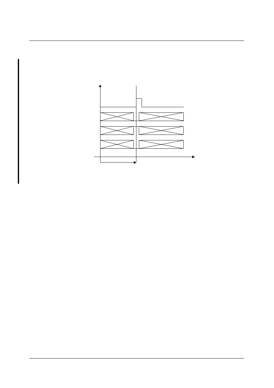
SDA 6000 / SDA 6001
PRELIMINARY DATA SHEET
Version 3.00
System Control & Configuration
6 - 40
Micronas
Figure 6-7
Leaving of testmode
TMODE
TMS
TDI
TCK
TMODE
TMS
TDI
TCK
Testmode active
TMODE
TMS
TDI
TCK
Testmode active

Peripherals

SDA 6000 / SDA 6001
PRELIMINARY DATA SHEET
Version 3.00
Peripherals
7 - 3
Micronas
7
Peripherals
All of the peripherals described in the following paragraphs are clocked with the same
clock as the CPU (
f
hw_clk
). Depending on the mode (normal or Idle), this frequency is
33.33 MHz or 3 MHz.

SDA 6000 / SDA 6001
PRELIMINARY DATA SHEET
Version 3.00
Peripherals
7 - 4
Micronas
7.1
General Purpose Timer Unit
The General Purpose Timer Unit (GPT) represents very flexible multifunctional timer
structures which may be used for timing, event counting, pulse width measurement,
pulse generation, frequency multiplication, and other purposes.
They incorporate five
16-bit timers that are grouped into the two timer blocks GPT1 and GPT2. Each timer in
each block may operate independently in a number of different modes such as gated
timer or counter mode, or may be concatenated with another timer of the same block.
Block 1 contains 3 timers/counters with a maximum resolution of
f
hw_clk
/4. The auxiliary
timers of GPT1 may be optionally configured as reload or capture registers for the core
timer.
Block 2 contains 2 timers/counters with a maximum resolution of
f
hw_clk
/2. An additional
CAPREL register supports capture and reload operations with extended functionality,
and its core timer T6 may be concatenated with the timers from the CAPCOM unit (T0
and T1).
The following enumeration summarizes all features to be supported:
Timer Block 1:
�
f
hw_clk
/4 maximum resolution
� 3 independent timers/counters
� Timers/counters can be concatenated
� 4 operating modes (timer, gated timer, counter, incremental)
� Separate interrupt nodes
Timer Block 2:
�
f
hw_clk
/2 maximum resolution
� 2 independent timers/counters
� Timers/counters can be concatenated
� 3 operating modes (timer, gated timer, counter)
� Extended capture/reload functions via 16-bit Capture/Reload register CAPREL
� Separate interrupt nodes
7.1.1
Functional Description of Timer Block 1
All three timers of block 1 (T2, T3, T4) can run in 4 basic modes, which are timer, gated
timer, counter and incremental interface mode. All timers can either count up or down.
Each timer has an input line (TxIN) associated with it which serves as the gate control in
gated timer mode, or as the count input in counter mode. The count direction (Up / Down)
may be programmed via software or dynamically altered by a signal at an external
control input line (TxEUD). An overflow/underflow of core timer T3 is indicated by the
output toggle latch T3OTL whose state may be output on related line T3OUT. The
auxiliary timers T2 and T4 may additionally be concatenated with the core timer, or used

SDA 6000 / SDA 6001
PRELIMINARY DATA SHEET
Version 3.00
Peripherals
7 - 5
Micronas
as capture or reload registers for the core timer. Concatenation of T3 with other timers
is provided through line T3OTL.
The current contents of each timer can be read or modified by the CPU by accessing the
corresponding timer registers T2, T3, or T4, which are located in the non-bitaddressable
SFR space. When any of the timer registers are written to by the CPU in the state
immediately before a timer increment, decrement, reload, or capture is to be performed,
the CPU write operation has priority in order to guarantee correct results.
Figure 7-1
Structure of Timer Block 1 Core Timer T3
The operation of the core timer T3 is controlled by its bit-addressable control register
T3CON.
Run Control
The timer can be started or stopped by software through bit T3R (Timer T3 Run Bit).
Setting bit T3R will start the timer, clearing T3R stops the timer.
UEB11195
2
n
: 1
2
n
: 1
2
n
: 1
hw_clk
f
T2EUD
T2IN
hw_clk
f
T3IN
T3EUD
T4IN
hw_clk
f
T4EUD
T3OTL
T3OTL
Control
Mode
T2
T3
Control
Mode
T4
Control
Mode
GPT1 Timer T2
U/D
Reload
Capture
GPT1 Timer T3
U/D
Capture
Reload
U/D
GPT1 Timer T4
Interrupt
Request
Interrupt
Request
Interrupt
Request

SDA 6000 / SDA 6001
PRELIMINARY DATA SHEET
Version 3.00
Peripherals
7 - 6
Micronas
In gated timer mode, the timer will only run if T3R is set and the gate is active (high or
low, as programmed).
Note: When bit T2RC/T4RC in timer control register T2CON/T4CON is set, T3R will also
control (start and stop) auxiliary timer T2/T4.
Count Direction Control
The count direction of the core timer can either be controlled by software or by the
external input line T3EUD (Timer T3 External Up/Down Control Input). These options are
selected by bits T3UD and T3UDE in control register T3CON. When the up/down control
is executed by software (bit T3UDE = `0'), the count direction can be altered by setting
or clearing bit T3UD. When T3UDE = `1', line T3EUD is selected to be the controlling
source of the count direction. However, bit T3UD can still be used to reverse the actual
count direction, as shown in the table below. If T3UD = `0' and line T3EUD shows a low
level, the timer is counting up. With a high level T3EUD, the timer is counting down. If
T3UD = `1', a high level at line T3EUD specifies counting up, and a low level specifies
counting down. The count direction can be changed regardless of whether the timer is
running or not.
When line T3EUD is used as external count direction control input, its associated port
pin must be configured as input.
Note: The direction control works in the same way for core timer T3 and for auxiliary
timers T2 and T4. Therefore the lines and bits are named Tx ...
Timer 3 Overflow/Underflow Monitoring
An overflow or underflow of timer T3 will clock the overflow toggle latch T3OTL in control
register T3CON. T3OTL can also be set or reset by software. Bit T3OE (Overflow/
Underflow Output Enable) in register T3CON enables the state of T3OTL to be
monitored via an external line T3OUT. If this line is linked to an external port pin, which
has to be configured as output, T3OTL can be used to control external HW.
Table 7-1
Core Timer T3 Count Direction Control
Line T3EUD Bit T3UDE
Bit T3UD
Count Direction
X
0
0
Count Up
X
0
1
Count Down
0
1
0
Count Up
1
1
0
Count Down
0
1
1
Count Down
1
1
1
Count Up

SDA 6000 / SDA 6001
PRELIMINARY DATA SHEET
Version 3.00
Peripherals
7 - 7
Micronas
In addition, T3OTL can be used in conjunction with the timer over/underflows as an input
for the counter function or as a trigger source for the reload function of the auxiliary
timers T2 and T4. For this purpose, the state of T3OTL does not have to be available at
any port pin, because an internal connection is provided for this option.
Timer 3 in Timer Mode
Timer mode for the core timer T3 is selected by setting bit field T3M in register T3CON
to `000
B
'.
In this mode, T3 is clocked with the system clock
f
hw_clk
divided by a programmable
prescaler, which is controlled by bit field T3I and BPS1. The input frequency
f
T3
for timer
T3 and its resolution
r
T3
are scaled linearly with lower module clock frequencies, as can
be seen from the following formula:
Table 7-2 gives an overview for timer resolutions depending on prescaler factors.
This formula also applies to the Gated Timer Mode of T3 and to the auxiliary timers T2
and T4 in timer and gated timer mode.
Table 7-2
f
MOD
=
33.33 MHz
Timer Input Selection T2I / T3I / T4I
000
B
000
B
001
B
010
B
011
B
100
B
101
B
110
B
111
B
FM =
1
0
0
0
0
0
0
0
0
Prescaler factor
4
8
16
32
64
128
256
512
1024
Input Frequency 2.08
MHz
4.16
MHz
2.08
MHz
1.04
MHz
521.83
kHz
260.41
kHz
130.20
kHz
65.10
kHz
32.55
kHz
Resolution
120
ns
240
ns
480
ns
960
ns
1.92
�
s
3.84
�
s
7.68
�
s
15.36
�
s
30.72
�
s
Period
7.86
ms
15.72
ms
31.45
ms
62.91
ms
125.82
ms
251.6
ms
503
ms
1
s
2.01
s
f
T3
=
f
hw_clk
BPS1
�
2
<T3I>
r
T3
[ms] =
f
hw_clk
[MHz]
BPS1
�
2
<T3I>
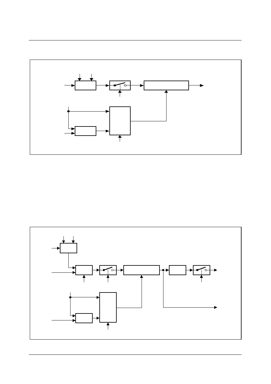
SDA 6000 / SDA 6001
PRELIMINARY DATA SHEET
Version 3.00
Peripherals
7 - 8
Micronas
Figure 7-2
Block Diagram of Core Timer T3 in Timer Mode
Timer 3 in Gated Timer Mode
The gated timer mode for the core timer T3 is selected by setting bit field T3M in register
T3CON to `010
B
' or `011
B
'.
Bit T3M.0 (T3CON.3) selects the active level of the gate input. In gated timer mode the
same options are available for the input frequency as for the timer mode. However, the
input clock to the timer in this mode is gated by the external input line T3IN (Timer T3
External Input); an associated port pin should be configured as input.
Figure 7-3
Block Diagram of Core Timer T3 in Gated Timer Mode
Core Timer Tx
TxEUD
TxUDE
MUX
EXOR
1
TxUD
hw_clk
f
TxR
: 1
BPS1
2
n
0
TxI
Down
Up/
UEB11196
Request
Interrupt
x = 3
Core Timer Tx
TxEUD
TxUDE
MUX
XOR
1
BPS1
TxUD
2
hw_clk
TxIN
f
TxR
: 1
MUX
0
TxI
n
Down
Up/
Request
Interrupt
UEB11197
TxOUT
TxOTL
TxOE
TxM
x = 3

SDA 6000 / SDA 6001
PRELIMINARY DATA SHEET
Version 3.00
Peripherals
7 - 9
Micronas
If T3M = `010
B
', the timer is enabled when T3IN shows a low level. A high level at this
line stops the timer. If T3M = `011
B
', line T3IN must have a high level in order to enable
the timer. In addition, the timer can be turned on or off by software using bit T3R. The
timer will only run, if T3R is set and the gate is active. It will stop, if either T3R is cleared
or the gate is inactive.
Note: A transition of the gate signal at line T3IN does not cause an interrupt request.
Timer 3 in Counter Mode
Counter mode for the core timer T3 is selected by setting bit field T3M in register T3CON
to `001
B
'. In counter mode, timer T3 is clocked by a transition at the external input line
T3IN. The event causing an increment or decrement of the timer can be a positive, a
negative, or both a positive and negative transition at this line. Bit field T3I in control
register T3CON selects the triggering transition (see table below).
Figure 7-4
Block Diagram of Core Timer T3 in Counter Mode
Table 7-3
Core Timer T3 (Counter Mode) Input Edge Selection
T3I
Triggering Edge for Counter Increment/Decrement
0 0 0
None. Counter T3 is disabled
0 0 1
Positive transition (rising edge) on T3IN
0 1 0
Negative transition (falling edge) on T3IN
0 1 1
Any transition (rising or falling edge) on T3IN
1 X X
Reserved. Do not use this combination
UEB11198
TxIN
TxI
Edge
Select
TxR
Core Timer Tx
Down
Up/
TxOUT
TxOTL
TxOE
TxEUD
XOR
TxUDE
MUX
1
TxUD
0
Request
Interrupt
TxOFL
x = 3
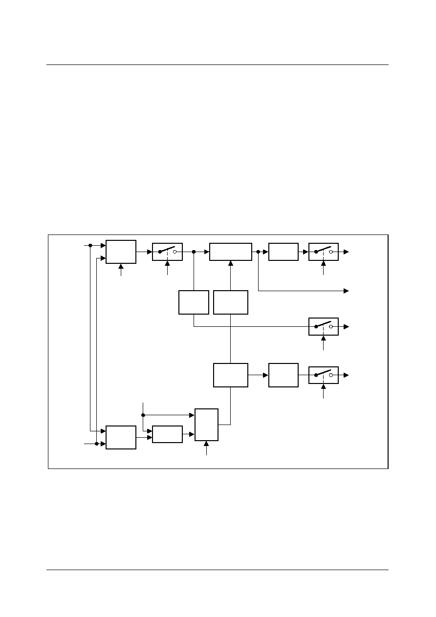
SDA 6000 / SDA 6001
PRELIMINARY DATA SHEET
Version 3.00
Peripherals
7 - 10
Micronas
For counter operation, a port pin associated to line T3IN must be configured as input.
The maximum input frequency which is allowed in counter mode is
f
hw_clk
/8 (BPS1 = `01').
To ensure that a transition of the count input signal which is applied to T3IN is correctly
recognized, its level should be held high or low for at least 4
f
hw_clk
cycles (BPS1 = `01')
before it changes.
Timer 3 in Incremental Interface Mode
Incremental Interface mode for the core timer T3 is selected by setting bit field T3M in
register T3CON to `110
B
' or `111
B
'. In Incremental Interface mode the two inputs
associated with timer T3 (T3IN, T3EUD) are used to interface to an incremental encoder.
T3 is clocked by each transition on one or both of the external input lines which gives 2-
fold or 4-fold the resolution of the encoder input.
Figure 7-5
Block Diagram of Core Timer T3 in Incremental Interface Mode
The T3I bit field in control register T3CON selects the triggering transitions (see Table 7-
4). In this mode, the sequence of the transitions of the two input signals is evaluated and
generates count pulses as well as the direction signal. Depending on the chosen
Incremental Interface Mode, rotation detection `110
B
' or edge detection `111
B
', an
interrupt is generated. For the rotation detection, an interrupt will be generated each time
the count direction of timer T3 changes. For the edge detection an interrupt will be
UEB11199
Select
Edge
T3I
Phase
Detect
T3IN
T3EUD
0
MUX
1
T3UD
T3
Edge
XOR
Timer T3
T3
RDIR
T3R
Up/
Down
T3OTL
T3OE
Interrupt
Request
T3UDE
T3OUT
Change
Detection
T3
CHDIR
T3M
T3M
Interrupt
Edge
Interrupt
Rotation
SDA 6000 / SDA 6001
PRELIMINARY DATA SHEET
Version 3.00
Peripherals
7 - 11
Micronas
generated each time a count action for timer T3 occurs. Count direction, changes in the
count direction and count requests are monitored through the status bits T3RDIR,
T3CHDIR and T3EDGE in register T3CON. T3 is modified automatically according to the
speed and the direction of the incremental encoder. Therefore, the contents of the T3
timer always represents the encoder's current position.
The incremental encoder can be connected directly to the microcontroller without
external interface logic. In a standard system, however, comparators will be employed
to convert the encoder's differential outputs (e.g. A, A) to digital signals (e.g. A). This
greatly increases noise immunity.
Note: The third encoder output T0, which indicates the mechanical zero position, may
be connected to an external interrupt input and trigger a reset of timer T3.
Figure 7-6
Interfacing the Encoder to the Microcontroller
For incremental interface operation the following conditions must be met:
� The T3M bit field must be `110
B
' or `111
B
'.
� Pins associated with lines T3IN and T3EUD must be configured as input.
� The T3UDE bit must be set to enable automatic direction control.
Table 7-4
Core Timer T3 (Incremental Interface Mode) Input Edge Selection
T3I
Triggering Edge for Counter Increment/Decrement
0 0 0
None. Counter T3 stops.
0 0 1
Any transition (rising or falling edge) on T3IN.
0 1 0
Any transition (rising or falling edge) on T3EUD.
0 1 1
Any transition (rising or falling edge) on any T3 input (T3IN or T3EUD).
1 X X
Reserved. Do not use this combination.
UED11136
-
+
+
-
+
-
A
B
T0
T3 Input
T3 Input
Interrupt
Microcontroller
A
A
B
B
T0
T0
External
Encoder
Signal Conditioning
SDA 6000 / SDA 6001
PRELIMINARY DATA SHEET
Version 3.00
Peripherals
7 - 12
Micronas
The maximum input frequency which is allowed in incremental interface mode is
f
hw_clk
/
8 (BPS = 01). To ensure that a transition of any input signal is correctly recognized, its
level should be held high or low for at least 4
f
hw_clk
cycles (BPS = 01) before it changes.
In Incremental Interface Mode the count direction is automatically derived from the
sequence in which the input signals change, which corresponds to the rotation direction
of the connected sensor. Table 7-5 summarizes the possible combinations.
The figures below give examples of T3's operation, visualizing count signal generation
and direction control. It also shows how input jitter is compensated, which might occur if
the sensor rests near to one of its switching points.
Figure 7-7
Evaluation of the Incremental Encoder Signals
Table 7-5
Core Timer T3 (Incremental Interface Mode) Count Direction
Level on
Respective other
Input
T3IN Input
T3EUD Input
Rising Falling Rising Falling
High
Down
Up
Up
Down
Low
Up
Down
Down
Up
UET11137
Up
Down
Up
Forward
Jitter
Backward
Jitter
Forward
T3IN
T3EUD
Contents
of T3
Note: This example shows the timer behavior assuming that T3 counts upon any transition on
any input, i.e. T3I = '011
B
'.
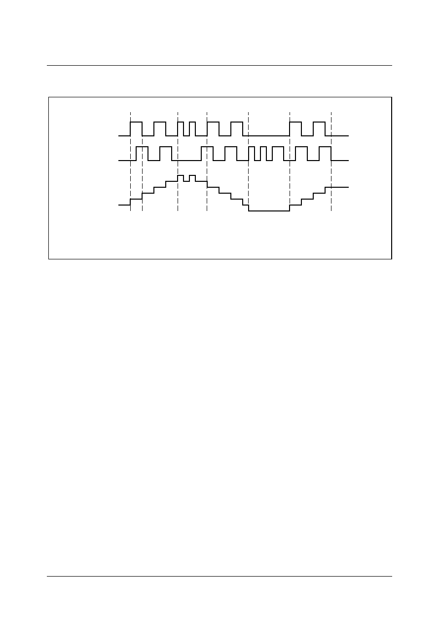
SDA 6000 / SDA 6001
PRELIMINARY DATA SHEET
Version 3.00
Peripherals
7 - 13
Micronas
Figure 7-8
Evaluation of the Incremental Encoder Signals
Note: Timer T3, operating in incremental interface mode, automatically provides
information on the sensor's current position. Dynamic information (speed,
acceleration, deceleration) may be obtained by measuring the incoming signal
periods.
Auxiliary Timers T2 and T4
Both auxiliary timers T2 and T4 have exactly the same functionality. They can be
configured for timer, gated timer, counter, or incremental interface mode with the same
options for the timer frequencies and the count signal as the core timer T3. In addition to
these 4 counting modes, the auxiliary timers can be concatenated with the core timer, or
they may be used as reload or capture registers in conjunction with the core timer.
The individual configuration for the T2 and T4 timers is determined by their bit-
addressable control registers T2CON and T4CON, which are both organized identically.
Note that functions which are present in all 3 timers of timer block 1 are controlled in the
same bit positions and in the same manner in each of the specific control registers.
Run control for auxiliary timers T2 and T4 can be handled by the associated Run Control
Bit T2R, T4R in register T2CON/T4CON. Alternatively, a remote control option (T2RC,
T4RC set) may be enabled to start and stop T2/T4 via the run bit T3R of core timer T3.
UET11138
Up
Down
Up
Forward
Jitter
Backward
Jitter
Forward
T3IN
T3EUD
Contents
of T3
Note: This example shows the timer behavior assuming that T3 counts upon any transition on
input T3IN, i.e. T3I = '001
B
'.

SDA 6000 / SDA 6001
PRELIMINARY DATA SHEET
Version 3.00
Peripherals
7 - 14
Micronas
Timers T2 and T4 in Timer Mode or Gated Timer Mode
When the auxiliary timers T2 and T4 are programmed to timer mode or gated timer
mode, their operation is the same as described for the core timer T3. The descriptions,
figures and tables apply accordingly with two exceptions:
� There is no TxOUT output line for T2 and T4.
� Overflow/Underflow Monitoring is not supported (no output toggle latch).
Timers T2 and T4 in Counter Mode
In counter mode timers T2 and T4 can be clocked either by a transition at the respective
external input line TxIN, or by a transition of timer T3's output toggle latch T3OTL.
Figure 7-9
Block Diagram of an Auxiliary Timer in Counter Mode
The event causing an increment or decrement of a timer can be a positive, a negative,
or both a positive and negative transition at either the respective input line, or at the
output toggle latch T3OTL.
Bit field TxI in the respective control register TxCON selects the triggering transition (see
Table 7-6).
UEB11200
TxI
Select
Edge
TxR
Auxiliary Timer Tx
Interrupt
Request
XOR
TxUDE
TxIN
TxEUD
MUX
TxUD
0
1
Up/
Down
x = 2, 4

SDA 6000 / SDA 6001
PRELIMINARY DATA SHEET
Version 3.00
Peripherals
7 - 15
Micronas
Note: Only state transitions of T3OTL which are caused by the overflows/underflows of
T3 will trigger the counter function of T2/T4. Modifications of T3OTL via software
will NOT trigger the counter function of T2/T4.
For counter operation, an external pin associated to line TxIN must be configured as
input. The maximum input frequency which is allowed in counter mode is
f
hw_clk
/8 (BPS1
= `01'). To ensure that a transition of the count input signal which is applied to TxIN is
correctly recognized, its level should be held for at least 4
f
hw_clk
cycles (BPS1 = `01')
before it changes.
7.1.1.1
Timer Concatenation
Using the output toggle latch T3OTL as a clock source for an auxiliary timer in counter
mode concatenates the core timer T3 with the respective auxiliary timer. Depending on
which transition of T3OTL is selected to clock the auxiliary timer, this concatenation
forms a 32-bit or a 33-bit timer/counter.
� 32-bit Timer/Counter: If both positive and negative transitions of T3OTL are used to
clock the auxiliary timer, this timer is clocked on every overflow/underflow of the core
timer T3. Thus, the two timers form a 32-bit timer.
� 33-bit Timer/Counter: If either a positive or a negative transition of T3OTL is selected
to clock the auxiliary timer, this timer is clocked on every second overflow/underflow
of the core timer T3. This configuration forms a 33-bit timer (16-bit core timer
+ T3OTL + 16-bit auxiliary timer).
The count directions of the two concatenated timers are not required to be the same.
This offers a wide variety of different configurations.
In this case T3 can operate in timer, gated timer or counter mode.
Table 7-6
Auxiliary Timer (Counter Mode) Input Edge Selection
T2I/T4I
Triggering Edge for Counter Increment/Decrement
X 0 0
None. Counter Tx is disabled
0 0 1
Positive transition (rising edge) on TxIN
0 1 0
Negative transition (falling edge) on TxIN
0 1 1
Any transition (rising or falling edge) on TxIN
1 0 1
Positive transition (rising edge) of output toggle latch T3OTL
1 1 0
Negative transition (falling edge) of output toggle latch T3OTL
1 1 1
Any transition (rising or falling edge) of output toggle latch T3OTL
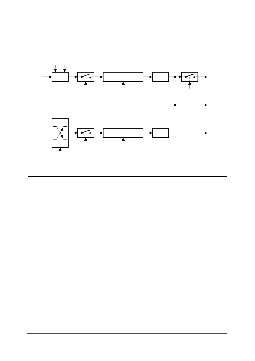
SDA 6000 / SDA 6001
PRELIMINARY DATA SHEET
Version 3.00
Peripherals
7 - 16
Micronas
Figure 7-10 Concatenation of Core Timer T3 and an Auxiliary Timer
Auxiliary Timer in Reload Mode
Reload mode for the auxiliary timers T2 and T4 is selected by setting bit field TxM in the
respective register TxCON to `100
B
'. In reload mode the core timer T3 is reloaded with
the contents of an auxiliary timer register, triggered by one of two different signals. The
trigger signal is selected the same way as the clock source for counter mode (see
Table 7-6), i.e. a transition of the auxiliary timer's input or the output toggle latch T3OTL
may trigger the reload.
Note: When programmed for reload mode, the respective auxiliary timer (T2 or T4) stops
independent of its run flag T2R or T4R.
UES11201
TxI
TxR
Select
Edge
Auxiliary Timer Tx
TxIR
Core Timer Ty
TyR
TyOTL
TyOE
Interrupt
Request
TyOUT
Up/Down
Interrupt
Request
x = 2, 4 y = 3
hw_clk
f
: 1
2
n
BPS1 TyI
)
*
Note: Line `*' is only affected by over/underflows of T3, but NOT by software
modifications of T3OTL.
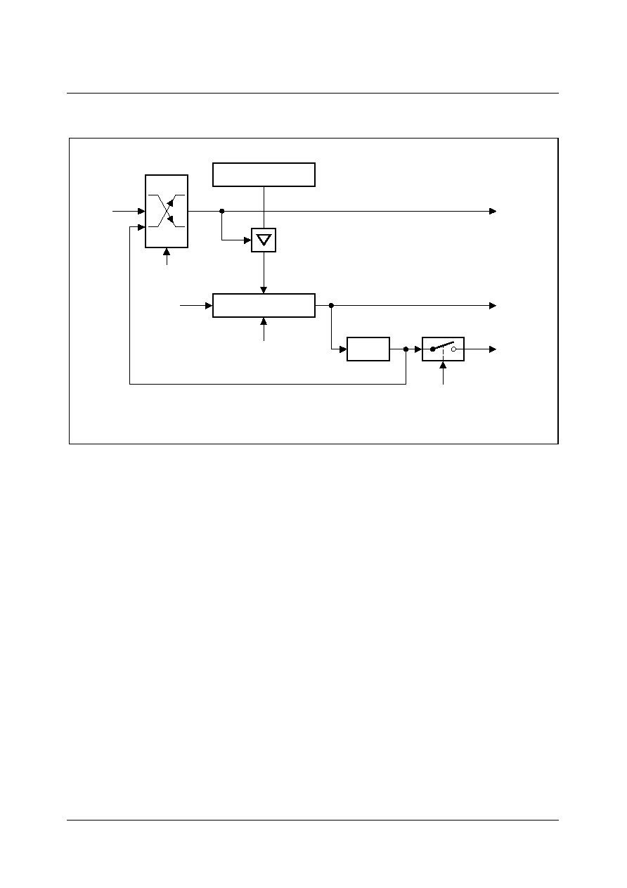
SDA 6000 / SDA 6001
PRELIMINARY DATA SHEET
Version 3.00
Peripherals
7 - 17
Micronas
Figure 7-11 GPT1 Auxiliary Timer in Reload Mode
Upon a trigger signal, T3 is loaded with the contents of the respective timer register (T2
or T4) and the interrupt request flag (T2IR or T4IR) is set.
Note: When a T3OTL transition is selected for the trigger signal, also the interrupt
request flag T3IR will be set upon a trigger, indicating T3's overflow or underflow.
Modifications of T3OTL via software will NOT trigger the counter function of T2/T4.
The reload mode triggered by T3OTL can be used in a number of different
configurations. Depending on the selected active transition the following functions can
be performed:
� If both a positive and a negative transition of T3OTL are selected to trigger a reload,
the core timer will be reloaded with the contents of the auxiliary timer each time it
overflows or underflows. This is the standard reload mode (reload on overflow/
underflow).
� If either a positive or a negative transition of T3OTL is selected to trigger a reload, the
core timer will be reloaded with the contents of the auxiliary timer on every second
overflow or underflow.
� Using this "single-transition" mode for both auxiliary timers allows very flexible pulse
width modulation (PWM) to be performed. One of the auxiliary timers is programmed
to reload the core timer on a positive transition of T3OTL, the other is programmed for
a reload on a negative transition of T3OTL. With this combination the core timer is
alternately reloaded from the two auxiliary timers.
UES11202
TxI
Select
Source/Edge
Reload Register Tx
Core Timer T3
Clock
Input
Up/Down
Request
Interrupt
Interrupt
Request
T3OE
T3OUT
TxIN
T3OTL
)
*
x = 2, 4
Note: Line `*' is only affected by over/underflows of T3, but NOT by software
modifications of T3OTL.
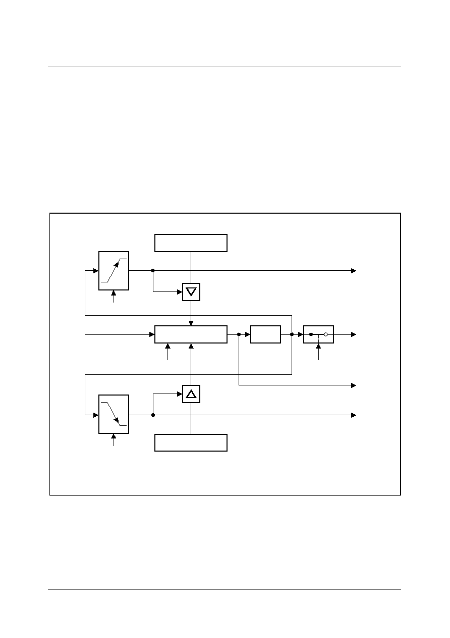
SDA 6000 / SDA 6001
PRELIMINARY DATA SHEET
Version 3.00
Peripherals
7 - 18
Micronas
Figure 7-12 shows an example of the generation of a PWM signal using the alternate
reload mechanism. T2 defines the high time of the PWM signal (reloaded on positive
transitions) and T4 defines the low time of the PWM signal (reloaded on negative
transitions). The PWM signal can be output on line T3OUT if the control bit T3OE is set.
With this method the high and low time of the PWM signal can be varied in a wide range.
Note: The output toggle latch T3OTL is accessible via software and may be changed, if
required, to modify the PWM signal. However, this will NOT trigger the reloading
of T3.
Note: An associated port pin linked to line T3OUT should be configured as output.
Figure 7-12 GPT1 Timer Reload Configuration for PWM Generation
Note: Although it is possible, selecting the same reload trigger event for both auxiliary
timers should be avoided. In this case both reload registers would try to load the
core timer at the same time. If this combination is selected, T2 is disregarded and
the contents of T4 reloaded.
UES11203
Reload Register T2
T2I
Core Timer T3
Input
Clock
Interrupt
Request
T3OTL
T3OUT
T3OE
T4I
Reload Register T4
Request
Interrupt
Request
Interrupt
Up/Down
)
*
)
*
Note: Lines `*' are only affected by over/underflows of T3, but NOT by software
modifications of T3OTL.
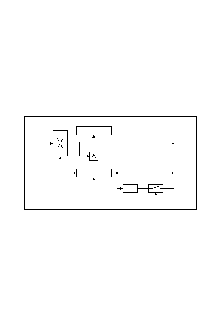
SDA 6000 / SDA 6001
PRELIMINARY DATA SHEET
Version 3.00
Peripherals
7 - 19
Micronas
Auxiliary Timer in Capture Mode
Capture mode for the auxiliary timers T2 and T4 is selected by setting bit field TxM in the
respective register TxCON to `101
B
'. In capture mode the contents of the core timer are
latched into an auxiliary timer register in response to a signal transition at the respective
auxiliary timer's external input line TxIN. The capture trigger signal can be a positive, a
negative, or both a positive and a negative transition.
The two least significant bits of bit field TxI are used to select the active transition (see
table in the counter mode section), while the most significant bit, TxI.2, is irrelevant for
capture mode. It is recommended to keep this bit cleared (TxI.2 = `0').
Note: When programmed for capture mode, the respective auxiliary timer (T2 or T4)
stops independent of its run flag T2R or T4R.
Figure 7-13 Auxiliary Timer of Timer Block 1 in Capture Mode
Upon a trigger (selected transition) at the corresponding input line TxIN the contents of
the core timer are loaded into the auxiliary timer register and the associated interrupt
request flag TxIR will be set.
Note: The direction control for T2IN and for T4IN must be set to `Input', and the level of
the capture trigger signal should be kept high or low for at least 4
f
hw_clk
(BPS1 = `01') cycles before it changes, to ensure correct edge detection.
UES11204
TxI
Select
Edge
Capture Register Tx
Core Timer T3
Clock
Input
Up/Down
Request
Interrupt
Interrupt
Request
T3OE
T3OUT
TxIN
T3OTL
x = 2, 4
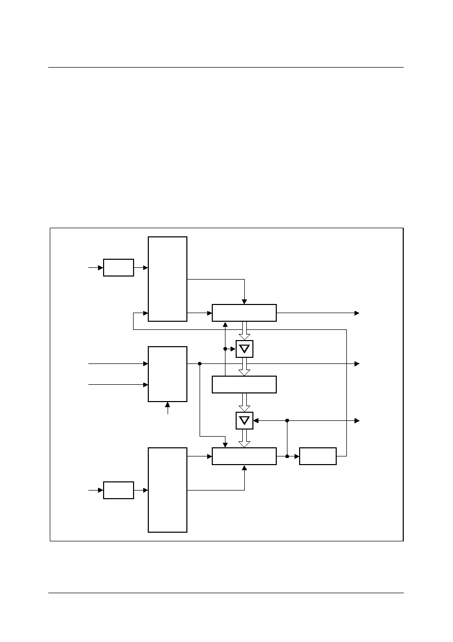
SDA 6000 / SDA 6001
PRELIMINARY DATA SHEET
Version 3.00
Peripherals
7 - 20
Micronas
7.1.2
Functional Description of Timer Block 2
Timer block 2 includes the two timers T5 (referred to as the auxiliary timer) and T6
(referred to as the core timer), and the 16-bit capture/reload register CAPREL.
The count direction (Up / Down) may be programmed by software. The auxiliary timer T6
may be reloaded with the contents of CAPREL.
The toggle bit (T6OTL) also supports the concatenation of T6 with auxiliary timer T5,
while concatenation of T6 with other timers is provided through line T6OFL. Triggered by
an external signal, the contents of T5 can be captured in register CAPREL, and T5 may
optionally be cleared. Both timer T6 and T5 can count up or down, and the current timer
value can be read or modified by the CPU in the non-bitaddressable SFRs T5 and T6.
Figure 7-14 Structure of Timer Block 2
UES11205
hw_clk
f
2 : 1
n
Mode
Control
T5
CAPIN
T3IN/
T3EUD
GPT2 Timer T5
U/D
MUX
CT3
Control
Mode
T6
hw_clk
f
: 1
2
n
GPT2 Timer T6
U/D
GPT2 CAPREL
Interrupt
Request
Request
Interrupt
Clear
Capture
Interrupt
Request
T6OTL
Clear

SDA 6000 / SDA 6001
PRELIMINARY DATA SHEET
Version 3.00
Peripherals
7 - 21
Micronas
7.1.2.1
Core Timer T6
The operation of the core timer T6 is controlled by its bit-addressable control register
T6CON.
Timer 6 Run Bit
The timer can be started or stopped by software through bit T6R (Timer T6 Run Bit).
Setting bit T6R will start the timer, clearing T6R stops the timer.
Note: When bit T5RC is set, bit T6R will also control (start and stop) auxiliary timer T5.
Count Direction Control
The count direction of the core timer can be controlled by software. The count direction
can be changed regardless of whether the timer is running or not.
Note: The direction control works the same for core timer T6 and for auxiliary timer T5.
Therefore the lines and bits are named Tx ...
Timer 6 Overflow/Underflow Monitoring
An overflow or underflow of timer T6 will clock the toggle latch T6OTL in control register
T6CON. T6OTL can also be set or reset by software. T6OTL can be used in conjunction
with the timer over/underflows as an input for the counter function of the auxiliary timer
T5.
Timer 6 in Timer Mode
Timer mode for the core timer T6 is selected by setting bit field T6M in register T6CON
to `000
B
'. In this mode, T6 is clocked with the module clock divided by a programmable
prescaler, which is selected by bit field T6I. The input frequency
f
T6
for timer T6 and its
resolution
r
T6
are scaled linearly with lower clock frequencies
f
hw_clk
, as can be seen from
the following formula:
Table 7-7
Core Timer T6 Count Direction Control
Bit TxUD
Count Direction
0
Count Up
1
Count Down
f
T6
=
f
hw_clk
BPS2
�
2
<T6I>
r
T6
[ms] =
f
hw_clk
[MHz]
BPS2
�
2
<T6I>
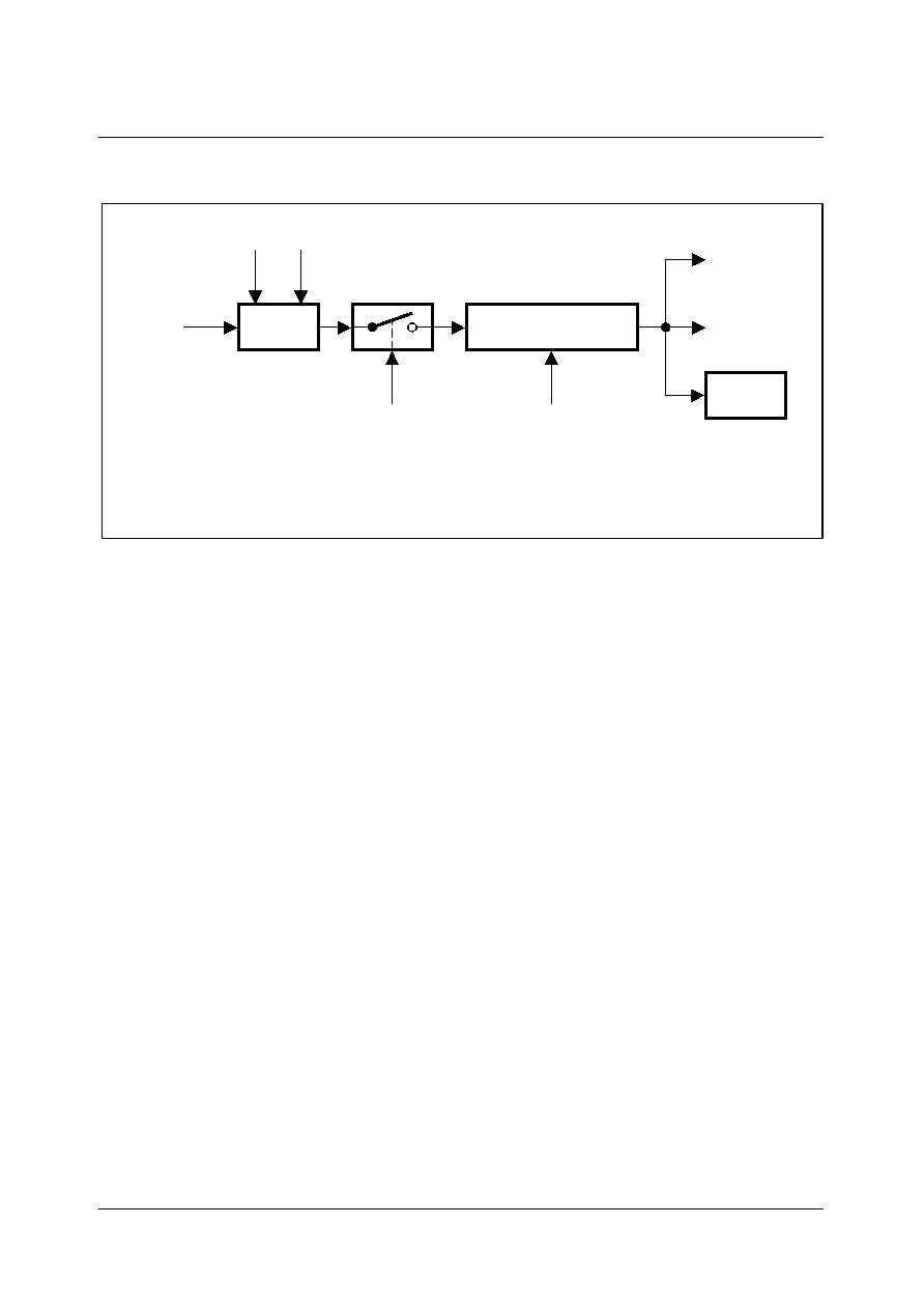
SDA 6000 / SDA 6001
PRELIMINARY DATA SHEET
Version 3.00
Peripherals
7 - 22
Micronas
Figure 7-15 Block Diagram of Core Timer T6 in Timer Mode
7.1.2.2
Auxiliary Timer T5
The auxiliary timer T5 can be configured for timer mode using the same options for the
timer frequencies and the count signal as the core timer T6. In addition to these 3
counting modes, the auxiliary timer can be concatenated with the core timer.
The individual configuration for timer T5 is determined by its bit-addressable control
register T5CON. Note that functions present in both timers of timer block 2 are controlled
in the same bit positions and manner in each of the specific control registers.
Run control for auxiliary timer T5 can be handled by the associated Run Control Bit T5R
in register T5CON. Alternatively, a remote control option (T5RC is set) may be enabled
to start and stop T5 via the run bit T6R of core timer T6.
Note: The auxiliary timer has no overflow/underflow toggle latch. Therefore, an output
line for Overflow/Underflow monitoring is not provided.
Count Direction Control for Auxiliary Timer
The count direction of the auxiliary timer can be controlled in the same way as for the
core timer T6. The description and the table apply accordingly.
Timer T5 in Timer Mode
When the auxiliary timer T5 is programmed to timer mode its operation is the same as
described for the core timer T6. The descriptions, figures and tables apply accordingly
with one exception:
� Overflow/Underflow monitoring is not supported (no output toggle latch).
Core Timer T6
hw_clk
f
T6R
: 1
BPS2
2
n
T6I
Down
Up/
UEB11206
T6OFL
Request
Interrupt
T6OTL
x = 6
T6UD
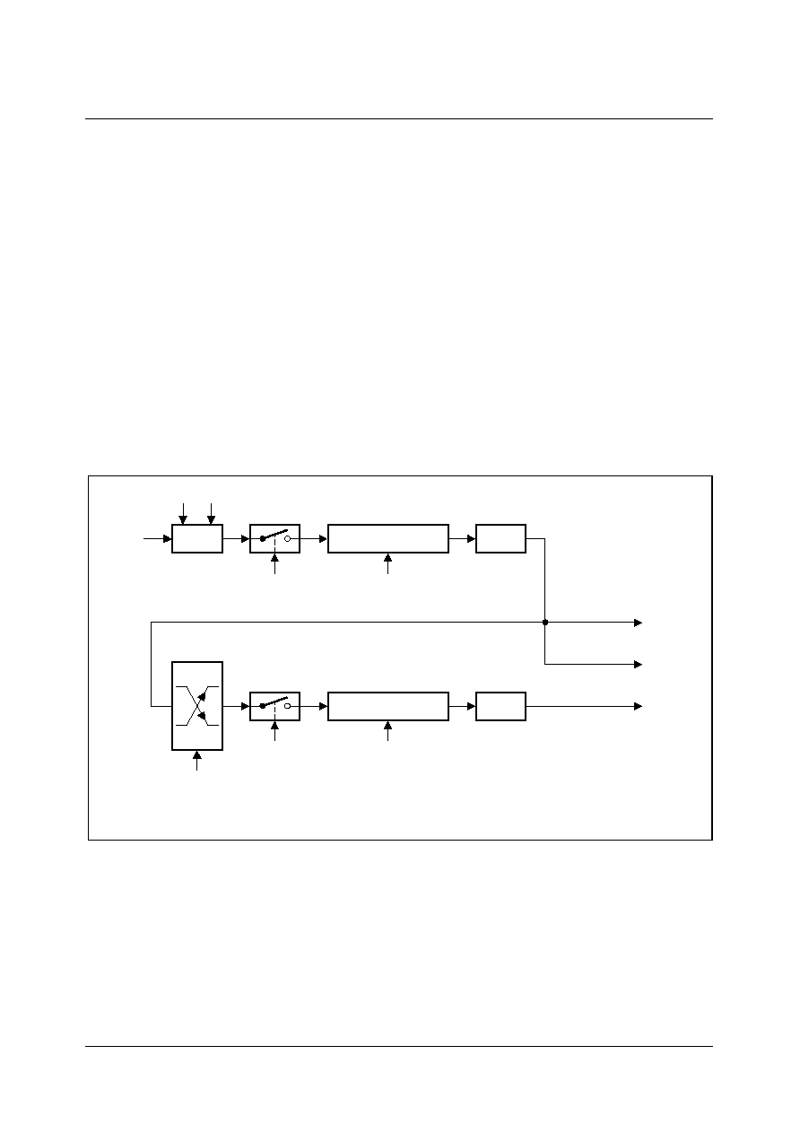
SDA 6000 / SDA 6001
PRELIMINARY DATA SHEET
Version 3.00
Peripherals
7 - 23
Micronas
7.1.2.3
Timer Concatenation
Using the toggle bit T6OTL as a clock source for the auxiliary timer in counter mode
concatenates the core timer T6 with the auxiliary timer. Depending on which transition of
T6OTL is selected to clock the auxiliary timer, this concatenation forms a 32-bit or a 33-
bit timer/counter.
� 32-bit Timer/Counter: If both positive and negative transitions of T6OTL are used to
clock the auxiliary timer, this timer is clocked on every overflow/underflow of the core
timer T6. Thus, the two timers form a 32-bit timer.
� 33-bit Timer/Counter: If either a positive or a negative transition of T6OTL is selected
to clock the auxiliary timer, this timer is clocked on every second overflow/underflow
of the core timer T6. This configuration forms a 33-bit timer (16-bit core timer
+ T6OTL + 16-bit auxiliary timer). The count directions of the two concatenated timers
are not required to be the same. This offers a wide variety of different configurations.
In this case T6 can operate in timer, gated timer or counter mode.
Figure 7-16 Concatenation of Core Timer T6 and Auxiliary Timer T5
Capture/Reload Register CAPREL in Capture Mode
This 16-bit register can be used as a capture register for the auxiliary timer T5. This
mode is selected by setting bit T5SC in control register T5CON. The CT3 bit selects the
external input line CAPIN or the input lines of timer T3 as the source for a capture trigger.
Either a positive, a negative, or both a positive and a negative transition at line CAPIN
can be selected to trigger the capture function, or transitions on input T3IN or input
UES11207
TxI
TxR
Select
Edge
Auxiliary Timer Tx
TxIR
Core Timer Ty
TyR
TyOTL
Interrupt
Request
Up/Down
Up/Down
Interrupt
Request
*
x = 5 y = 6
hw_clk
f
: 1
2
n
BPS2 TyI
TyOFL
)
Note: Line `*' is only affected by over/underflows of T6, but NOT by software
modifications of T6OTL.
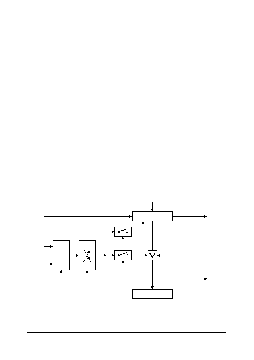
SDA 6000 / SDA 6001
PRELIMINARY DATA SHEET
Version 3.00
Peripherals
7 - 24
Micronas
T3EUD or both inputs T3IN and T3EUD. The active edge is controlled by bit field CI in
register T5CON.
The maximum input frequency for the capture trigger signal at CAPIN is
f
hw_clk
/2
(BPS2 = `01'). To ensure that a transition of the capture trigger signal is correctly
recognized, its level should be held for at least 2
f
hw_clk
cycles (BPS2 = `01') before it
changes.
When the timer T3 capture trigger is enabled (CT3 is set), register CAPREL captures the
contents of T5 when transitions of the selected input(s) occur. These values can be used
to measure T3's input signals. This is useful e.g. when T3 operates in incremental
interface mode, in order to derive dynamic information (speed acceleration) from the
input signals.
When a selected transition at the external input line CAPIN is detected, the contents of
the auxiliary timer T5 are latched into register CAPREL, and interrupt request flag CRIR
is set. At the same time, timer T5 can be cleared to 0000
H
. This option is controlled by
bit T5CLR in register T5CON. If T5CLR = `0', the contents of timer T5 are not affected
by a capture. If T5CLR = `1', timer T5 is cleared after the current timer value has been
latched into register CAPREL.
Note: Bit T5SC only controls whether a capture is performed or not. If T5SC = `0', the
input line CAPIN can still be used to clear timer T5 or as an external interrupt input.
This interrupt is controlled by the CAPREL interrupt control register CRIC.
Figure 7-17 Timer Block 2 Register CAPREL in Capture Mode
UEB11208
Auxiliary Timer T5
Up/Down
Interrupt
Request
Interrupt
Request
T5CLR
T5SC
T5CC
Edge
Select
CI
MUX
CAPREL Register
CAPIN
T3IN/
T3EUD
Input
Clock
CT3

SDA 6000 / SDA 6001
PRELIMINARY DATA SHEET
Version 3.00
Peripherals
7 - 25
Micronas
Timer Block 2 Capture/Reload Register CAPREL in Reload Mode
This 16-bit register can be used as a reload register for the core timer T6. This mode is
selected by setting bit T6SR = `1' in register T6CON. The operation causing a reload in
this mode is an overflow or underflow of the core timer T6.
When timer T6 overflows from FFFF
H
to 0000
H
(when counting up) or when it underflows
from 0000
H
to FFFF
H
(when counting down), the value stored in register CAPREL is
loaded into timer T6. This will not set the interrupt request flag CRIR associated with the
CAPREL register. However, interrupt request flag T6IR will be set indicating the
overflow/underflow of T6.
Figure 7-18 Timer Block 2 Register CAPREL in Reload Mode
Timer Block 2 Capture/Reload Register CAPREL in Capture-And-Reload Mode
Since the reload function and the capture function of register CAPREL can be enabled
individually by bits T5SC and T6SR, by setting both bits the two functions can be enabled
simultaneously. This feature can be used to generate an output frequency that is a
multiple of the input frequency.
UEB11209
Up/Down
Input
Clock
CAPREL Register
Core Timer T6
T6SR
Request
Interrupt
T6OFL

SDA 6000 / SDA 6001
PRELIMINARY DATA SHEET
Version 3.00
Peripherals
7 - 26
Micronas
Figure 7-19 Timer Block 2 Register CAPREL in Capture-And-Reload Mode
This combined mode can be used to detect consecutive external events which may
occur aperiodically, but where a finer resolution, i.e. more `ticks' within the time between
two external events, is required.
For this purpose, the time between the external operations is measured using timer T5
and the CAPREL register. Timer T5 runs in timer mode counting up with a frequency of
e.g.
f
hw_clk
/32. The external operations are applied to line CAPIN. When an external
operation occurs, the timer T5 contents are latched into register CAPREL, and timer T5
is cleared (T5CLR = `1'). Thus, register CAPREL always contains the correct time
between two operations, measured in timer T5 increments. Timer T6, which runs in timer
mode counting down with a frequency of e.g.
f
hw_clk
/4, uses the value in register CAPREL
to perform a reload on underflow. This means that the value in register CAPREL
represents the time between two underflows of timer T6, now measured in timer T6
increments. Since timer T6 runs 8 times faster than timer T5, it will underflow 8 times
within the time between two external operations. Thus, the underflow signal of timer T6
generates 8 `ticks'. Upon each underflow, the interrupt request flag T6IR will be set and
UEB11210
Auxiliary Timer T5
Up/Down
Interrupt
Request
Interrupt
Request
T5CLR
T5SC
T5CC
Edge
Select
CI
MUX
CAPREL Register
CAPIN
T3IN/
T3EUD
Input
Clock
CT3
Up/Down
Input
Clock
Core Timer T6
T6SR
Request
Interrupt
T6OFL
T6CLR

SDA 6000 / SDA 6001
PRELIMINARY DATA SHEET
Version 3.00
Peripherals
7 - 27
Micronas
bit T6OTL will be toggled. This signal has 8 times more transitions than the signal which
is applied to line CAPIN.
A certain deviation of the output frequency is generated by the fact that timer T5 will
count actual time units (e.g. T5 running at 1 MHz will capture the value 64
H
/100
D
for a
10 KHz input signal) while T6OTL will only toggle on an underflow of T6 (i.e. the
transition from 0000
H
to FFFF
H
). In the above mentioned example, T6 would count down
from 64
H
so the underflow would occur after 101 T6 timing ticks. The actual output
frequency then is 79.2 KHz instead of the expected 80 KHz.
This can be solved by activating the capture correction (T5CC = `1'). If the capture
correction is actived the content of T5 is decremented by 1 before being captured. The
deviation described is eliminated (in the example T5 would capture 63
H
/99
D
and the
output frequency would be 80 KHz).
The underflow signal of timer T6 can furthermore be used to clock one or more of the
CAPCOM unit's timers, which gives the user the possibility to set compare operations
based on a finer resolution than that of the external operations. This connection is
accomplished through the T6OFL signal.
7.1.3
GPT Registers
All available kernel registers are summarized in Table 7-8.
Function Control Registers
The operating mode of the core timer T3 is configured and controlled by its bit-
addressable control register T3CON.
Table 7-8
GPT Register Summary
Name
Reset Value
Description
T2CON
0000
H
Timer 2 Control Register
T3CON
0000
H
Timer 3 Control Register
T4CON
0000
H
Timer 4 Control Register
T5CON
0000
H
Timer 5 Control Register
T6CON
0000
H
Timer 6 Control Register
CAPREL
0000
H
Capture/Reload Register
T2
0000
H
Timer 2 Register
T3
0000
H
Timer 3 Register
T4
0000
H
Timer 4 Register
T5
0000
H
Timer 5 Register
T6
0000
H
Timer 6 Register

SDA 6000 / SDA 6001
PRELIMINARY DATA SHEET
Version 3.00
Peripherals
7 - 28
Micronas
T3CON
Timer 3 Control Register
15
14
13
12
11
10
9
8
7
6
5
4
3
2
1
0
T3
RDI
R
T3
CH
DIR
T3
EDG
E
T3
BPS1
T3
OTL
T3
OE
T3
UDE
T3
UD
T3R
T3M
T3I
rh
rwh rwh
rw
rwh
rw
rw
rw
rw
rw
rw
Field
Bits
Type Description
T3I
[2:0]
rw
Timer 3 Input Parameter Selection
Timer mode see Table 7-9 for encoding
Gated Timer see Table 7-9 for encoding
Counter mode see Table 7-10 for encoding
Incremental Interface mode see Table 7-11 for
encoding
T3M
[5:3]
rw
Timer 3 Mode Control
000 Timer Mode
001 Counter Mode
010 Gated Timer with Gate active low
011 Gated Timer with Gate active high
100 Reserved. Do not use this combination!
101 Reserved. Do not use this combination!
110 Incremental Interface Mode (Rotation
detection)
111 Incremental Interface Mode (Edge detection)
T3R
[6]
rw
Timer 3 Run Bit
0
Timer/Counter 3 stops
1
Timer/Counter 3 runs
T3UD
[7]
rw
Timer 3 Up/Down Control
(when T3UDE = `0')
0
Counting `Up'
1
Counting `Down'
T3UDE
[8]
rw
Timer 3 External Up/Down Enable
0
Counting direction is internally controlled by
SW
1
Counting direction is externally controlled by
line T3EUD

SDA 6000 / SDA 6001
PRELIMINARY DATA SHEET
Version 3.00
Peripherals
7 - 29
Micronas
T3OE
[9]
rw
Overflow/Underflow Output Enable
0
T3 overflow/underflow can not be externally
monitored
1
T3 overflow/underflow may be externally
monitored via T3OUT
T3OTL
[10]
rwh
Timer 3 Output Toggle Latch
Toggles on each overflow/underflow of T3. Can be
set or reset by software.
BPS1
[12:11] rw
Timer Block Prescaler 1
The maximum input frequency
00
For Timer 2/3/4 is
f
hw_clk
/8
01
For Timer 2/3/4 is
f
hw_clk
/4
10
For Timer 2/3/4 is
f
hw_clk
/32
11
For Timer 2/3/4 is
f
hw_clk
/16
T3EDGE
[13]
rwh
Timer 3 Edge Detection
The bit is set on each successful edge detection.
The bit has to be reset by SW.
0
No count edge was detected
1
A count edge was detected
T3CHDIR
[14]
rwh
Timer 3 Count Direction Change
The bit is set on a change of the count direction of
timer 3. The bit has to be reset by SW.
0
No change in count direction was detected
1
A change in count direction was detected
T3RDIR
[15]
rh
Timer 3 Rotation Direction
0
Timer 3 counts up
1
Timer 3 counts down
Field
Bits
Type Description

SDA 6000 / SDA 6001
PRELIMINARY DATA SHEET
Version 3.00
Peripherals
7 - 30
Micronas
Table 7-9
Timer 3 Input Parameter Selection for Timer Mode and Gated Mode
T3I
Prescaler for
f
hw_clk
(BPS1 = 00)
Prescaler for
f
hw_clk
(BPS1 = 01)
Prescaler for
f
hw_clk
(BPS1 = 10)
Prescaler for
f
hw_clk
(BPS1 = 11)
000
8
4
32
16
001
16
8
64
32
010
32
16
128
64
011
64
32
256
128
100
128
64
512
256
101
256
128
1024
512
110
512
256
2048
1024
111
1024
512
4096
2048
Table 7-10
Timer 3 Input Parameter Selection for Counter Mode
T3I
Triggering Edge for Counter Update
000
None. Counter T3 is disabled
001
Positive transition (raising edge) on T3IN
010
Negative transition (falling edge) on T3IN
011
Any transition (raising or falling edge) on T3IN
1XX
Reserved. Do not use this combination!
Table 7-11
Timer 3 Input Parameter Selection for Incremental Interface Mode
T3I
Triggering Edge for Counter Update
000
None. Counter T3 stops
001
Any transition (raising or falling edge) on T3IN
010
Any transition (raising or falling edge) on T3EUD
011
Any transition (raising or falling edge) on T3IN or T3EUD
1XX
Reserved. Do not use this combination!

SDA 6000 / SDA 6001
PRELIMINARY DATA SHEET
Version 3.00
Peripherals
7 - 31
Micronas
T2CON
T4CON
Timer 2/4 Control Register
15
14
13
12
11
10
9
8
7
6
5
4
3
2
1
0
Tx
RDIR
Tx
CH
DIR
Tx
EDG
E
Tx
IR
DIS
0
Tx
RC
Tx
UDE
Tx
UD
TxR
TxM
TxI
rh
rwh rwh
rw
r
rw
rw
rw
rw
rw
rw
Field
Bits
Type Description
TxI
[2:0]
rw
Timer x Input Parameter Selection
Timer mode see Table 7-12 for encoding
Gated Timer see Table 7-12 for encoding
Counter mode see Table 7-13 for encoding
Incremental Interface mode see Table 7-14 for
encoding
TxM
[5:3]
rw
Timer x Mode Control (Basic Operating Mode)
000 Timer Mode
001 Counter Mode
010 Gated Timer with Gate active low
011 Gated Timer with Gate active high
100 Reload Mode
101 Reserved. Do not use this combination!
110 Incremental Interface Mode (Rotation
detection)
111 Incremental Interface Mode (Edge detection)
TxR
[6]
rw
Timer x Run Bit
0
Timer/Counter x stops
1
Timer/Counter x runs
TxUD
[7]
rw
Timer x Up/Down Control
(when TxUDE = `0')
0
Counting `Up'
1
Counting `Down'
TxUDE
[8]
rw
Timer x External Up/Down Enable
0
Counting direction is internally controlled by
SW
1
Counting direction is externally controlled by
line TxEUD

SDA 6000 / SDA 6001
PRELIMINARY DATA SHEET
Version 3.00
Peripherals
7 - 32
Micronas
TxRC
[9]
rw
Timer x Remote Control
0
Timer/Counter x is controlled by its own run bit
TxR
1
Timer/Counter x is controlled by the run bit of
core timer 3
TxIRDIS
[12]
rw
Timer x Interrupt Disable
0
Interrupt generation for TxCHDIR and
TxEDGE interrupts in Incremental Interface
Mode is enabled
1
Interrupt generation for TxCHDIR and
TxEDGE interrupts in Incremental Interface
Mode is disabled
TxEDGE
[13]
rwh
Timer x Edge Detection
The bit is set on each successful edge detection.
The bit has to be reset by SW.
0
No count edge was detected
1
A count edge was detected
TxCHDIR
[14]
rwh
Timer x Count Direction Change
The bit is set on a change of the count direction of
timer x. The bit has to be reset by SW.
0
No change in count direction was detected
1
A change in count direction was detected
TxRDIR
[15]
rh
Timer x Rotation Direction
0
Timer x counts up
1
Timer x counts down
Field
Bits
Type Description

SDA 6000 / SDA 6001
PRELIMINARY DATA SHEET
Version 3.00
Peripherals
7 - 33
Micronas
Table 7-12
Timer x Input Parameter Selection for Timer Mode and Gated Mode
T3I
Prescaler for
f
hw_clk
(BPS1 = 00)
Prescaler for
f
hw_clk
(BPS1 = 01)
Prescaler for
f
hw_clk
(BPS1 = 10)
Prescaler for
f
hw_clk
(BPS1 = 11)
000
8
4
32
16
001
16
8
64
32
010
32
16
128
64
011
64
32
256
128
100
128
64
512
256
101
256
128
1024
512
110
512
256
2048
1024
111
1024
512
4096
2048
Table 7-13
Timer x Input Parameter Selection for Counter Mode
TxI
Triggering Edge for Counter Update
X 0 0
None. Counter Tx is disabled
0 0 1
Positive transition (raising edge) on TxIN
0 1 0
Negative transition (falling edge) on TxIN
0 1 1
Any transition (raising or falling edge) on TxIN
1 0 1
Positive transition (rising edge) of output toggle latch T3OTL
1 1 0
Negative transition (falling edge) of output toggle latch T3OTL
1 1 1
Any transition (rising or falling edge) of output toggle latch
T3OTL
Table 7-14
Timer x Input Parameter Selection for Incremental Interface Mode
TxI
Triggering Edge for Counter Update
000
None. Counter Tx stops
001
Any transition (raising or falling edge) on TxIN
010
Any transition (raising or falling edge) on TxEUD
011
Any transition (raising or falling edge) on TxIN or TxEUD
1XX
Reserved. Do not use this combination!

SDA 6000 / SDA 6001
PRELIMINARY DATA SHEET
Version 3.00
Peripherals
7 - 34
Micronas
T6CON
Timer 6 Control Register
15
14
13
12
11
10
9
8
7
6
5
4
3
2
1
0
T6
SR
T6
CLR
0
BPS2
T6
OTL
0
0
T6
UD
T6R
T6M
T6I
rw
rw
r
rw
rwh
rw
rw
rw
rw
rw
rw
Field
Bits
Type Description
T6I
[2:0]
rw
Timer 6 Input Parameter Selection
Timer mode see Table 7-15 for encoding
T6M
[5:3]
rw
Timer 6 Mode Control (Basic Operating Mode)
000 Timer Mode
001 Reserved. Do not use this combination!
010 Reserved. Do not use this combination!
011 Reserved. Do not use this combination!
1XX Reserved. Do not use this combination!
T6R
[6]
rw
Timer 6 Run Bit
0
Timer/Counter 6 stops
1
Timer/Counter 6 runs
T6UD
[7]
rw
Timer 6 Up/Down Control
0
Counting `Up'
1
Counting `Down'
T6OTL
[10]
rwh
Timer 6 Output Toggle Latch
Toggles on each overflow/underflow of T6. Can be
set or reset by software.
BPS2
[12:11] rw
Timer Block Prescaler 2
The maximum input frequency
00
For Timer 5/6 is
f
hw_clk
/4
01
For Timer 5/6 is
f
hw_clk
/2
10
For Timer 5/6 is
f
hw_clk
/16
11
For Timer 5/6 is
f
hw_clk
/8
T6CLR
[14]
rw
Timer 6 Clear Bit
0
Timer 6 is not cleared on a capture event
1
Timer 6 is cleared on a capture event
T6SR
[15]
rw
Timer 6 Reload Mode Enable
0
Reload from register CAPREL disabled
1
Reload from register CAPREL enabled

SDA 6000 / SDA 6001
PRELIMINARY DATA SHEET
Version 3.00
Peripherals
7 - 35
Micronas
Table 7-15
Timer 6 Input Parameter Selection for Timer Mode and Gated Mode
T6I Prescaler for
f
hw_clk
(BPS2 = 00)
Prescaler for
f
hw_clk
(BPS2 = 01)
Prescaler for
f
hw_clk
(BPS2 = 10)
Prescaler for
f
hw_clk
(BPS2 = 11)
000 4
2
16
8
001 8
4
32
16
010 16
8
64
32
011 32
16
128
64
100 64
32
256
128
101 128
64
512
256
110 256
128
1024
512
111 512
256
2048
1024
Table 7-16
Timer 6 Input Parameter Selection for Counter Mode
T6I
Triggering Edge for Counter Update
000
None. Counter T6 is disabled
001
Reserved. Do not use this combination!
010
Reserved. Do not use this combination!
011
Reserved. Do not use this combination!
1XX
Reserved. Do not use this combination!

SDA 6000 / SDA 6001
PRELIMINARY DATA SHEET
Version 3.00
Peripherals
7 - 36
Micronas
T5CON
Timer 5 Control Register
15
14
13
12
11
10
9
8
7
6
5
4
3
2
1
0
T5
SR
T5
CLR
CI
T5
CC
CT3
T5
RC
0
T5
UD
T5R
T5M
T5I
rw
rw
rw
rw
rw
rw
rw
rw
rw
rw
rw
Field
Bits
Type Description
T5I
[2:0]
rw
Timer 5 Input Parameter Selection
Timer mode see Table 7-17 for encoding
Counter mode see Table 7-18 for encoding
T5M
[5:3]
rw
Timer 5 Mode Control (Basic Operating Mode)
000 Timer Mode
001 Counter Mode
010 Reserved. Do not use this combination!
011 Reserved. Do not use this combination!
1XX Reserved. Do not use this combination!
T5R
[6]
rw
Timer 5 Run Bit
0
Timer/Counter 5 stops
1
Timer/Counter 5 runs
T5UD
[7]
rw
Timer 5 Up/Down Control
0
Counting `Up'
1
Counting `Down'
T5RC
[9]
rw
Timer 5 Remote Control
0
Timer/Counter x is controlled by its own run bit
T5R
1
Timer/Counter 5 is controlled by the run bit of
core timer 6
CT3
[10]
rw
Timer 3 Capture Trigger Enable
0
Capture trigger from input line CAPIN
1
Capture trigger from T3 input lines
T5CC
[11]
rw
Timer 5 Capture Correction
0
T5 is just captured without any correction
1
T5 is decremented by 1 before being captured
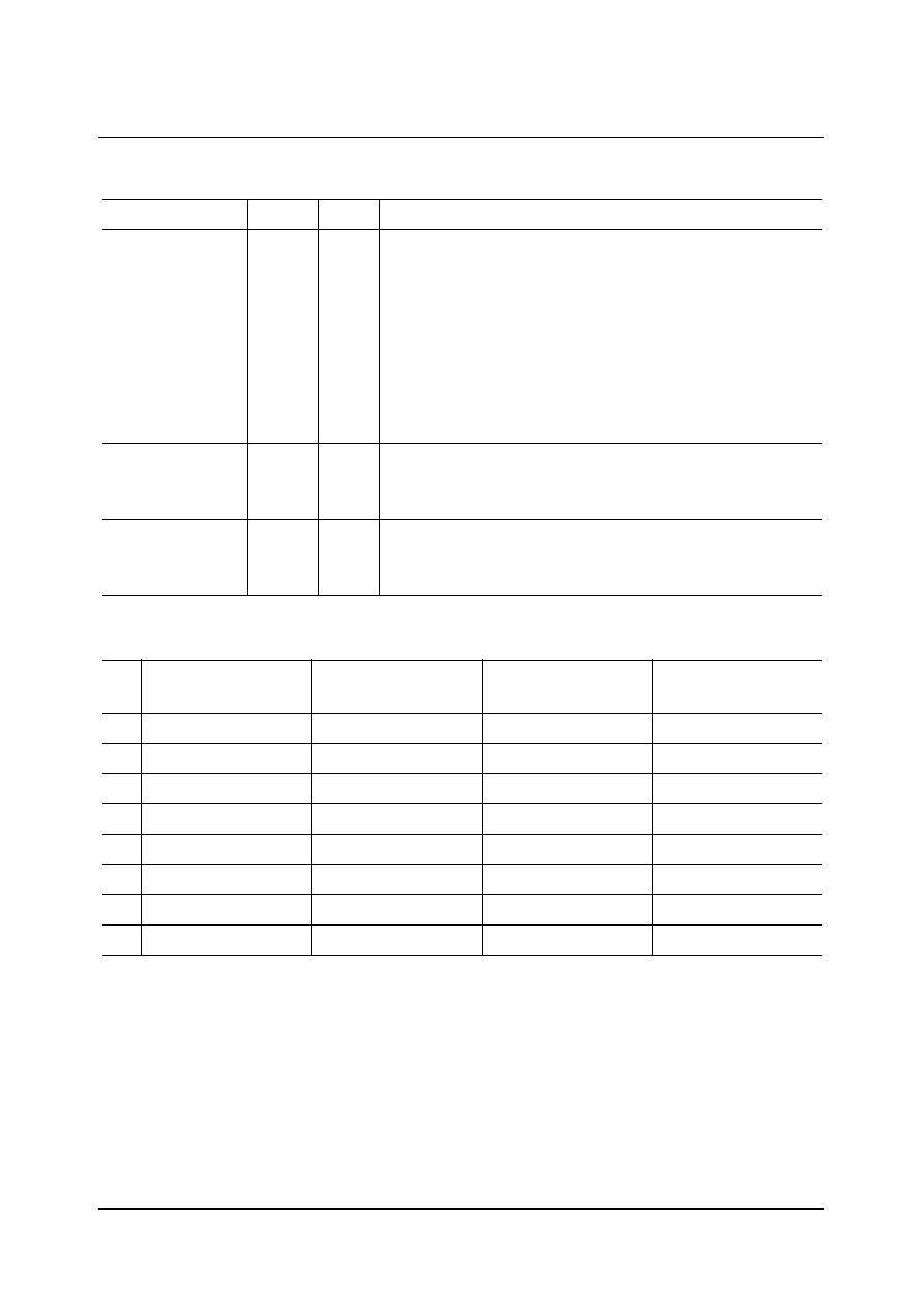
SDA 6000 / SDA 6001
PRELIMINARY DATA SHEET
Version 3.00
Peripherals
7 - 37
Micronas
CI
[13:12] rw
Register CAPREL Capture Trigger Selection
(depending in bit CT3)
00
Capture disabled
01
Positive transition (rising edge) on CAPIN or
any transition on T3IN
10
Negative transition (falling edge) on CAPIN or
any transition on T3EUD
11
Any transition (rising or falling edge) on CAPIN
or any transition on T3IN or T3EUD
T5CLR
[14]
rw
Timer 5 Clear Bit
0
Timer 5 is not cleared on a capture operation
1
Timer 5 is cleared on a capture operation
T5SC
[15]
rw
Timer 5 Capture Mode Enable
0
Capture into register CAPREL disabled
1
Capture into register CAPREL enabled
Table 7-17
Timer 5 Input Parameter Selection for Timer Mode and Gated Mode
T5I Prescaler for
f
hw_clk
(BPS2 = 00)
Prescaler for
f
hw_clk
(BPS2 = 01)
Prescaler for
f
hw_clk
(BPS2 = 10)
Prescaler for
f
hw_clk
(BPS2 = 11)
000 4
2
16
8
001 8
4
32
16
010 16
8
64
32
011 32
16
128
64
100 64
32
256
128
101 128
64
512
256
110 256
128
1024
512
111 512
256
2048
1024
Field
Bits
Type Description
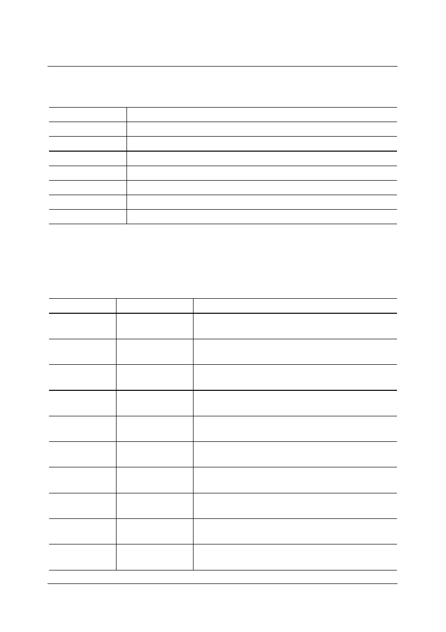
SDA 6000 / SDA 6001
PRELIMINARY DATA SHEET
Version 3.00
Peripherals
7 - 38
Micronas
7.1.4
Interrupts
For a detailed description of the various interrupts see description above. An overview is
given with a Table 7-19:
.
Table 7-18
Timer 5 Input Parameter Selection for Counter Mode
T5I
Triggering Edge for Counter Update
X00
None. Counter T5 is disabled
001
Reserved. Do not use this combination.
010
Reserved. Do not use this combination.
011
Reserved. Do not use this combination.
101
Positive transition (rising edge) of output toggle latch T6OTL
110
Negative transition (falling edge) of output toggle latch T6OTL
111
Any transition (rising or falling edge) of output toggle latch T6OTL
Table 7-19
Peripheral Name Interrupt Sources
Interrupt
Interrupt Node
Description
Timer 2
Overflow
T2IC
Interrupt is requested on overflow of timer 2 if
counting up.
Timer 2
Underflow
T2IC
Interrupt is requested on underflow of timer 2 if
counting down.
Timer 3
Overflow
T3IC
Interrupt is requested on overflow of timer 3 if
counting up.
Timer 3
Underflow
T3IC
Interrupt is requested on underflow of timer 3 if
counting down.
Timer 4
Overflow
T4IC
Interrupt is requested on overflow of timer 4 if
counting up.
Timer 4
Underflow
T4IC
Interrupt is requested on underflow of timer 4 if
counting down.
Timer 5
Overflow
T5IC
Interrupt is requested on overflow of timer 5 if
counting up.
Timer 5
Underflow
T5IC
Interrupt is requested on underflow of timer 5 if
counting down.
Timer 6
Overflow
T6IC
Interrupt is requested on overflow of timer 6 if
counting up.
Timer 6
Underflow
T6IC
Interrupt is requested on underflow of timer 6 if
counting down.

SDA 6000 / SDA 6001
PRELIMINARY DATA SHEET
Version 3.00
Peripherals
7 - 39
Micronas
Rotation
Direction
Change Timer 2
T2IC
Interrupt is requested on a change of the count
direction in the Incremental Interface Mode
(T2I = 110).
Edge Detection
Timer 2
T2IC
Interrupt is requested on a successful detected
edge resulting in a timer count action (T2I = 111).
Rotation
Direction
Change Timer 3
T3IC
Interrupt is requested on a change of the count
direction in the Incremental Interface Mode
(T3I = 110).
Edge Detection
Timer 3
T3IC
Interrupt is requested on a successful detected
edge resulting in a timer count action (T3I = 111).
Rotation
Direction
Change Timer 4
T4IC
Interrupt is requested on a change of the count
direction in the Incremental Interface Mode
(T4I = 110).
Edge Detection
Timer 4
T4IC
Interrupt is requested on a successful detected
edge resulting in a timer count action (T4I = 111).
Reload Action
Timer 2
T2IC
Interrupt is requested on a trigger signal for
reloading timer 3 in Reload Mode (T2I = 100).
Reload Action
Timer 4
T4IC
Interrupt is requested on a trigger signal for
reloading timer 3 in Reload Mode (T4I = 100).
Capture Action
Timer 2
T2IC
Interrupt is requested on a trigger signal for a
capture action to capture timer 3 in timer 2
Capture Mode (T2I = 101).
Capture Action
Timer 4
T4IC
Interrupt is requested on a trigger signal for a
capture action to capture timer 3 in timer 4
Capture Mode (T4I = 101).
Capture Action
Timer Block 2
CRIC
Interrupt is requested on a trigger signal for a
capture action of timer 5 to register CAPREL in
Capture Mode (T5SC = 1).
Table 7-19
Peripheral Name Interrupt Sources (cont'd)
Interrupt
Interrupt Node
Description
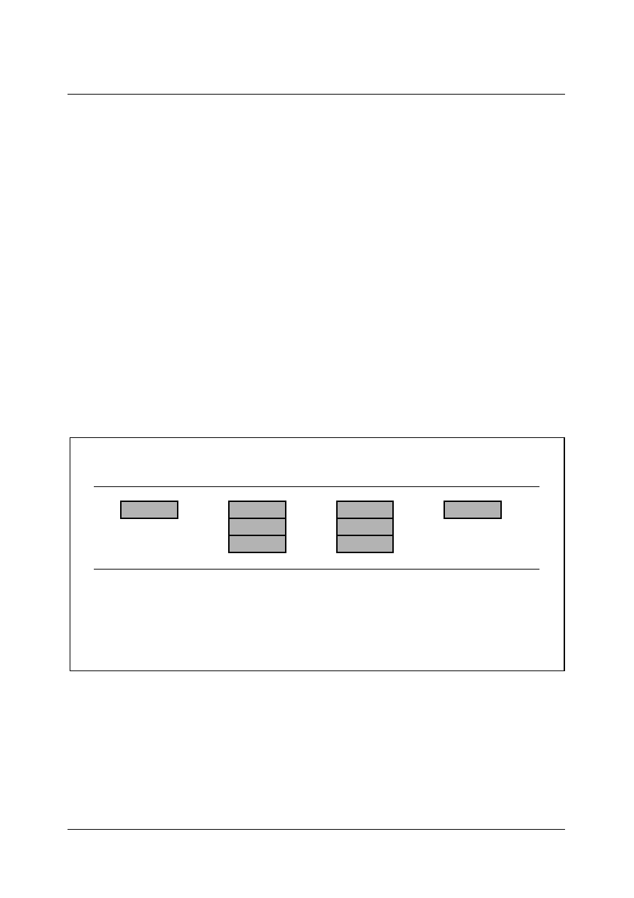
SDA 6000 / SDA 6001
PRELIMINARY DATA SHEET
Version 3.00
Peripherals
7 - 40
Micronas
7.2
Real-time Clock
7.2.1
General Description
The Real Time Clock (RTC) module of M2 is basically an independent timer chain and
counts time ticks. The base frequency of the RTC can be programmed via a reload
counter. The RTC can work fully asynchronous to the system frequency (33.33 MHz)
and is optimized on a low power consumption.
The RTC serves different purposes:
� Real-time clock to determine the current time and date
� Cyclic time based interrupt
� Alarm interrupt for wake up on a defined time
� 48-bit timer for long term measurements
The real time clock module provides three different types of registers: a control register
for controlling the RTC�s functionality, three data registers for setting the clock divider for
RTC base frequency programming and for flexible interrupt generation, and three
counter registers that contain the actual time and date. The interrupts are programmed
via one interrupt subnode register and via an interrupt node register.
Figure 7-20 RTC Register Overview
The RTC module consists of a chain of 2 divider blocks, the reloadable 16-bit timer T14
and the 32-bit RTC timer (accessible via registers RTCH and RTCL). Both timers count
up. Timer T14 is reloaded with the value of register T14REL on every T14 timer overflow.
T14REL is transparent during reload state.
Figure 7-21 shows the RTC block diagram:
RTC Interrupt Sub Node Control Register
UEA11139
RTC Timer Reload Register, High Word
Timer T14 Reload Register
RTC Control Register
Control Registers
RTC Timer Reload Register, Low Word
Timer T14 Count Register
RTCCON
RTCRELL
RTCRELH
RTCCON
T14REL
T14
RTCISNC
RTCL
RTCH
Counter Registers
Data Registers
RTCRELH
RTCRELL
T14REL
RTC Timer Count Register, High Word
RTC Timer Count Register, Low Word
RTCL
RTCH
T14
Interrupt Control
RTCISNC
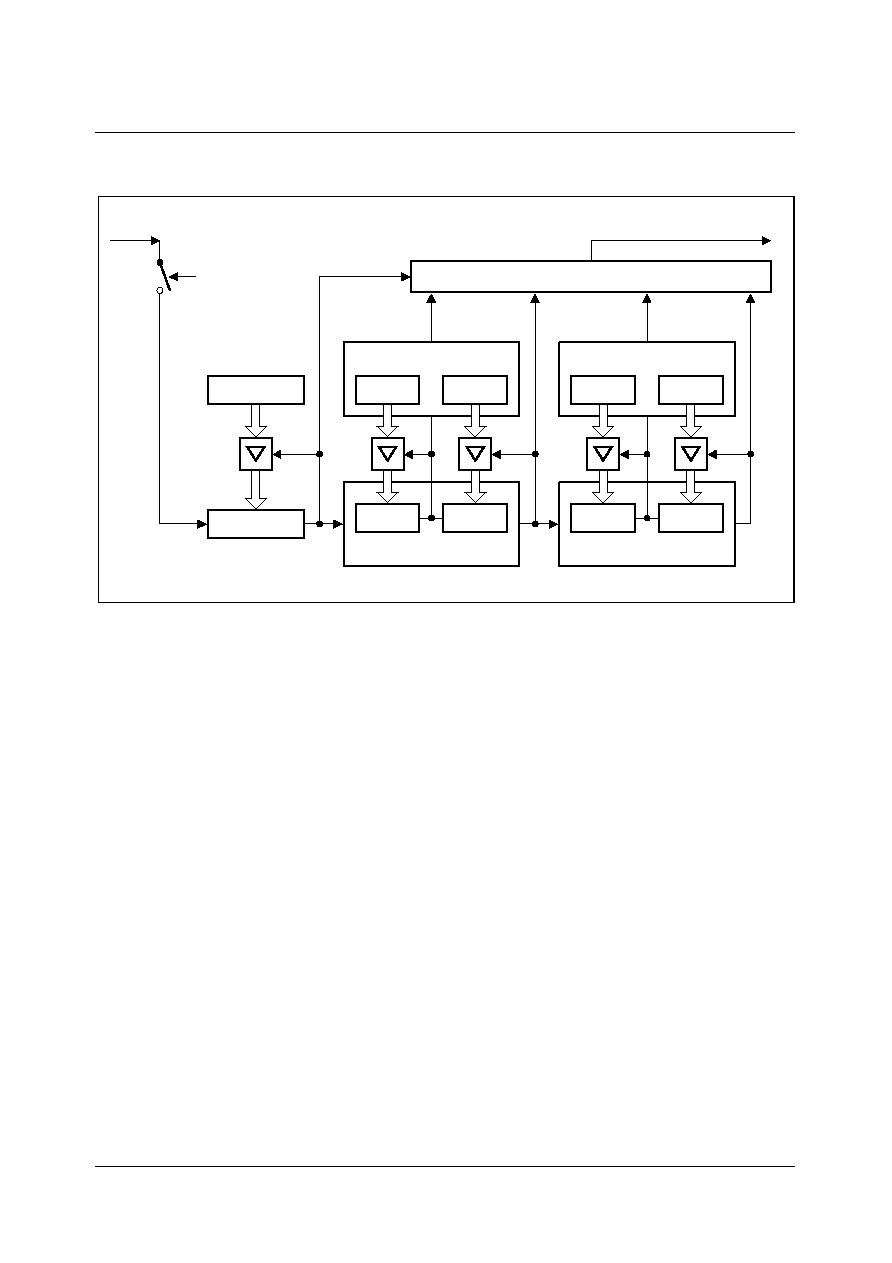
SDA 6000 / SDA 6001
PRELIMINARY DATA SHEET
Version 3.00
Peripherals
7 - 41
Micronas
Figure 7-21 RTC Block Diagram
RTC Control
The operating behavior of the RTC module is controlled by the RTCCON register. The
RTC starts counting by setting the RTCR run bit. After reset, the run bit is set and the
RTC automatically starts operation. Setting bits T14DEC or T14INC allows the T14 timer
to be manually and asynchronously decremented or incremented. These bits are cleared
by hardware after the decrement/increment operation. The RTC is only reset in case of
a hardware reset, so it keeps on running during idle and sleep mode.
Cyclic Interrupt Generation
The RTC module can generate an interrupt request RTC_INT whenever timer T14
overflows and is reloaded. This interrupt request may be used, for example, to provide
a system time tick, independent of the CPU clock frequency, without loading the general
purpose timers, or to wake up regularly from idle mode. The T14 overflow interrupt
(RTC_T14INT) cycle time can be adjusted via the timer T14 reload register T14REL. The
32 bit timer (RTCL and RTCH) can be divided into smaller reloadable timers. Each sub-
timer can be programmed for an overflow on different time bases (e.g. second, hour,
minute, day). With each timer overflow an RTC interrupt is generated. All these RTC
interrupts are ored within the RTC module via the interrupt subnode RTCISNC to one
interrupt request RTC_INT. This interrupt RTC_INT is one source of another interrupt
subnode ISNC in the interrupt controller. The other interrupt input of subnode ISNC is
disconnected in the M2. With typical values of T14REL = F448
H
, RTCRELL = 1018
H
and
UEB11140
10 Bit
10 Bit
6 Bit
6 Bit
RTCRELL0
RTCRELL1
RTCL1
RTCL0
RTC0INT
RTC1INT
RTC3INT
RTC2INT
RTCH2
RTCREL2
6 Bit
6 Bit
10 Bit
RTCH3
10 Bit
RTCREL3
Interrupt Subnode
RTC_INT
T14REL(16 Bit)
T14(16 Bit)
RTCR
3 MHz
T14_IN
RTC_T14INT
SDA 6000 / SDA 6001
PRELIMINARY DATA SHEET
Version 3.00
Peripherals
7 - 42
Micronas
RTCRELH = FA04
H
, counter T14 generates one overflow per millisecond, RTCL0 one
per second, RTCL1 one per minute, RTCH2 one per hour and RTCH3 one per day.
48-bit Timer Operation
The concatenation of the 16-bit reload timer T14 and the 32-bit RTC timer can be
regarded as a 48-bit timer which counts with the RTC count input frequency (3 MHz).
The reload registers T14REL, RTCRELL and RTCRELH should be cleared to get a 48-
bit binary timer. However, any other reload values may be used.
Interrupt Subnode RTCISNC
All RTC interrupts are connected to one interrupt node via an interrupt subnode. For this
interrupt sharing each interrupt source has, in addition to the node enable and request
flag its own enable and request flag located in register RTCISNC. After an RTC interrupt
(RTC_INT) is arbitrated, the interrupt service routine has to check all the enabled
sources request flags and run the respective software routine. The request flags have to
be deleted by software before leaving the interrupt service routine.
Reset Behavior
The RTC registers are only cleared or set by a hardware reset. Bit RTCR is set when the
hardware is reset.
7.2.2
Register Description
RTCCON
Reset Value: 8003
H
Bit
Function
RTCR
RTC Run Bit
`0':
RTC stops
`1':
RTC runs
T14DEC
Decrement T14 Timer Value
Setting this bit to 1 effects a decrement of the T14 timer value. The bit is
cleared by hardware after decrementation.
T14INC
Increment T14 Timer Value
Setting this bit to 1 effects an increment of the T14 timer value. The bit is
cleared by hardware after incrementation.
5
4
3
2
1
0
11
10
9
8
7
6
15
14
13
12
rw
rw
rw
-
-
-
-
-
-
-
-
-
-
-
-
T14
INC
T14
DEC
0
RTC
R
SDA 6000 / SDA 6001
PRELIMINARY DATA SHEET
Version 3.00
Peripherals
7 - 43
Micronas
Note: Bit RTCR is set on hardware reset.
T14
Reset Value: 0000
H
T14REL
Reset Value: 0000
H
RTCL
Reset Value: 0000
H
Bit
Function
TIMER14
(15 ... 0)
16 Bit Timer Register
Timer T14 generates the input clock for the RTC register and the periodic
interrupt.
Bit
Function
TIMERREL14
(15 ... 0)
16 Bit Reload Register for Timer 14
Represents the 16 bit reload value for T14
Bit
Function
RTCL1
(5 ... 0)
Low Word of 32 Bit Capture Register.
RTCL0
(9 ... 0)
5
4
3
2
1
0
11
10
9
8
7
6
15
14
13
12
rw
TIMER14(15 ..0 )
5
4
3
2
1
0
11
10
9
8
7
6
15
14
13
12
rw
TIMER14REL(15 ..0 )
5
4
3
2
1
0
11
10
9
8
7
6
15
14
13
12
rw
RTCL1(5 .. 0)
RTCL0(9 .. 0)

SDA 6000 / SDA 6001
PRELIMINARY DATA SHEET
Version 3.00
Peripherals
7 - 44
Micronas
RTCH
Reset Value: 0000
H
RTCRELL
Reset Value: 0000
H
RTCRELH
Reset Value: 0000
H
Bit
Function
RTCH3
(9 ... 0)
High Word of 32 Bit Capture Register.
RTCH2
(5 ... 0)
Bit
Function
RTCRELL1
(5 ... 0)
Low Word of 32 Bit Reload Register.
RTCRELL0
(9 ... 0)
Bit
Function
RTCRELH2
(5 ... 0)
High Word of 32 Bit Reload Register.
RTCRELH3
(9 ... 0)
5
4
3
2
1
0
11
10
9
8
7
6
15
14
13
12
rw
RTCH3(9.. 0)
RTCH2(5 .. 0)
5
4
3
2
1
0
11
10
9
8
7
6
15
14
13
12
rw
RTCRELL1(5 .. 0)
RTCRELL0(9 .. 0)
5
4
3
2
1
0
11
10
9
8
7
6
15
14
13
12
rw
RTCRELH3(9.. 0)
RTCRELH2(5 .. 0)

SDA 6000 / SDA 6001
PRELIMINARY DATA SHEET
Version 3.00
Peripherals
7 - 45
Micronas
RTC Interrupt Subnode Control
RTCISNC
Reset Value: 0000
H
Bit
Function
T14IR
T14 Overflow Interrupt Request Flag
`0':
No request pending.
`1':
This source has raised an interrupt request.
T14IE
T14 Overflow Interrupt Enable Control Bit
`0':
Interrupt request is disabled.
`1':
Interrupt request is enabled.
RTCxIR
RTCx Interrupt Request Flag
`0':
No request pending.
`1':
This source has raised an interrupt request.
RTCxIE
RTCx Interrupt Enable Control Bit
`0':
Interrupt request is disabled.
`1':
Interrupt request is enabled.
5
4
3
2
1
0
11
10
9
8
7
6
15
14
13
12
rw
rw
rw
rw
rw
rw
rw
rw
rw
rw
-
-
-
-
-
-
RTC
3 IR
RTC
3IE
RTC
2 IR
RTC
2IE
RTC
1 IR
RTC
1 IE
RTC
0 IR
RTC
0IE
T14
IR
T14
IE

SDA 6000 / SDA 6001
PRELIMINARY DATA SHEET
Version 3.00
Peripherals
7 - 46
Micronas
ISNC
Reset Value: 0000
H
Note: The interrupt request flags of both RTC interrupt subnodes have to be cleared by
software inside the interrupt service routine.
Bit
Function
RTCINTIR
RTC Interrupt Request Flag
`0':
No request pending.
`1': RTC
has
raised
an interrupt request.
RTCINTIE
RTC Interrupt Enable Control Bit
`0':
Interrupt request is disabled.
`1':
Interrupt request is enabled.
INT2IR
Interrupt Request Flag of 2nd Source
disconnected in M2.
INT2IE
2nd Source Interrupt Enable Control Bit
`0': recommended
value.
5
4
3
2
1
0
11
10
9
8
7
6
15
14
13
12
rw
rw
rw
-
-
-
-
-
-
-
-
-
-
-
-
INT2
IE
INT2
IR
RTC
INT
IE
RTC
INT
IR
rw

SDA 6000 / SDA 6001
PRELIMINARY DATA SHEET
Version 3.00
Peripherals
7 - 47
Micronas
7.3
Asynchronous/Synchronous Serial Interface
The Asynchronous/Synchronous Serial Interface ASC0 provides serial communication
between M2 and other microcontrollers, microprocessors or external peripherals. It
provides the following features:
� Full duplex asynchronous operating modes
� 8- or 9-bit data frames, LSB first
� Parity bit generation/checking
� One or two stop bits
� Baud rate from 2.0625 MBaud to 0.48 Baud (@ 33 MHz clock)
� Multiprocessor mode for automatic address/data byte detection
� Loop-back capability
� Support for IrDA data transmission/reception up to max. 115.2 KBaud
� Autobaud detection unit for asynchronous operating modes
� Detection of standard baud rates
1200, 2400, 4800, 9600, 19200, 38400, 57600, 115200, 230400 Baud
� Detection of non-standard baud rates
� Detection of asynchronous modes
7 bit, even parity; 7 bit, odd parity;
8 bit, even parity; 8 bit, odd parity; 8 bit, no parity
� Automatic initialization of control bits and baud rate generator after detection
� Detection of a serial two-byte ASCII character frame
� Half-duplex 8-bit synchronous operating mode
� Baud rate from 4.125 MBaud to 420 Baud (@ 33 MHz clock)
� Double buffered transmitter/receiver
� Interrupt generation
� on a transmitter buffer empty condition
� on a transmit last bit of a frame condition
� on a receiver buffer full condition
� on an error condition (frame, parity, overrun error)
� on the start and the end of a autobaud detection
Figure 7-22 shows a block diagram of the ASC with its operating modes (asynchronous
and synchronous mode.)
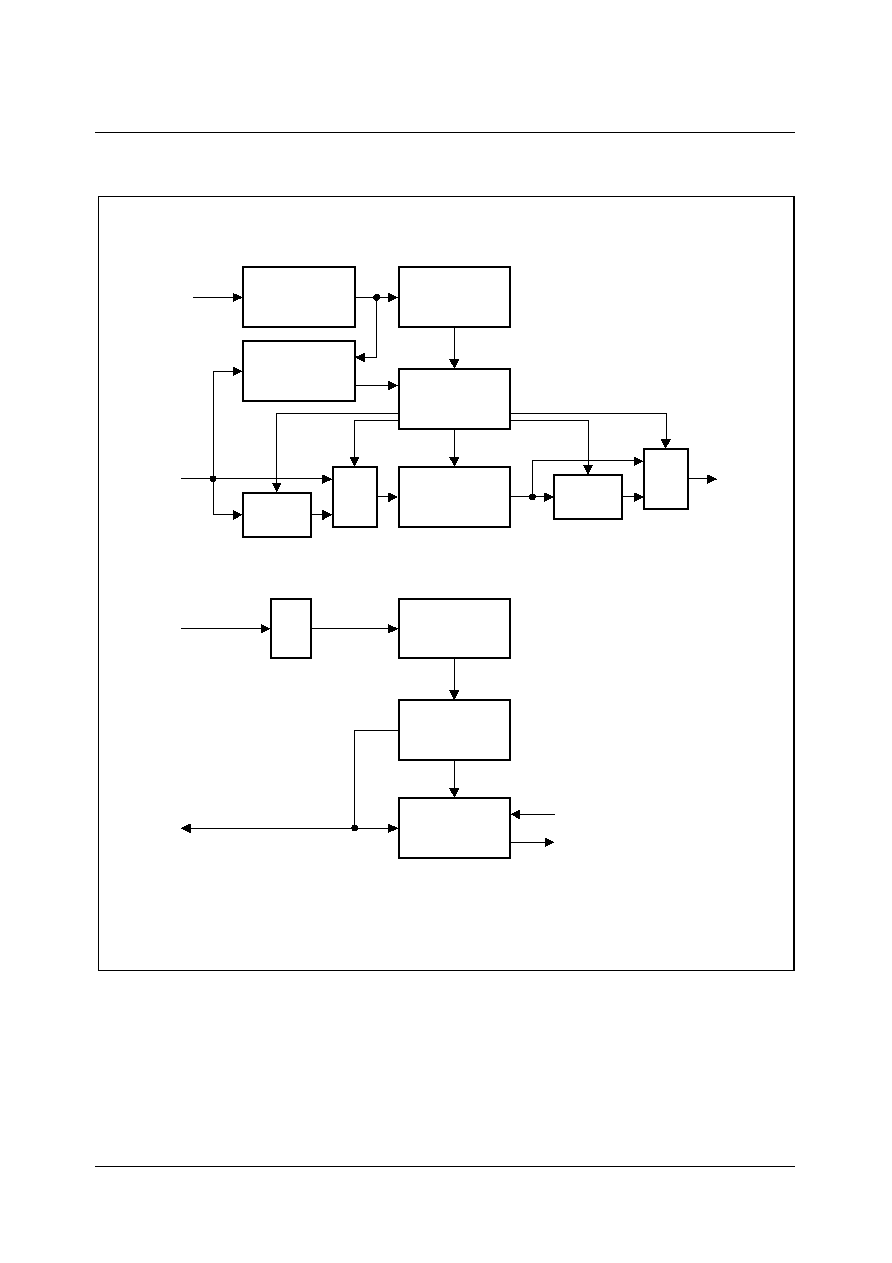
SDA 6000 / SDA 6001
PRELIMINARY DATA SHEET
Version 3.00
Peripherals
7 - 48
Micronas
.
Figure 7-22 Block Diagram of the ASC0
UEB11141
Receive/Transmit
Buffers and
Shift Registers
Serial Port
Control
Baud Rate
Timer
Prescaler/
Fractional Divider
Detection
Autobaud
DIV
f
Coding
IrDA
MUX
Decoding
IrDA
MUX
TxD
RxD
33 MHz
2
�
� 3
or
Serial Port
Control
Buffers and
Shift Registers
Receive/Transmit
Baud Rate
Timer
f
MOD
TxD
Shift Clock
RxDO
RxDI
Note: RxDI and RxDO are concatenated in the port logic to pin RxD.
Asynchronous Mode
Synchronous Mode
SDA 6000 / SDA 6001
PRELIMINARY DATA SHEET
Version 3.00
Peripherals
7 - 49
Micronas
Figure 7-23 ASC Register Overview
The ASC0 supports full-duplex asynchronous communication up to 2.08 MBaud and
half-duplex synchronous communication up to 4.16 MBaud (@ 33.33 MHz CPU clock).
In synchronous mode, data is transmitted or received synchronous to a shift clock which
is generated by the microcontroller. In asynchronous mode, 8- or 9-bit data transfer,
parity generation, and the number of stop bits can be selected. Parity, framing, and
overrun error detection is provided to increase the reliability of data transfers.
Transmission and reception of data is double-buffered. For multiprocessor
communication, a mechanism to distinguish address from data bytes is included. Testing
is supported by a loop-back option. A 13-bit baud rate timer with a versatile input clock
divider circuitry provides the ASC0 with the serial clock signal. In a special asynchronous
mode, the ASC0 supports IrDA data transmission up to 115.2 KBaud with fixed or
programmable IrDA pulse width.
A transmission is started by writing to the Transmit Buffer register S0TBUF (by way of
an instruction or a PEC data transfer). Only the number of data bits which is determined
by the selected operating mode, will actually be transmitted, e.g. bits written to positions
9 through 15 of register S0TBUF are always insignificant.
Data transmission is double-buffered, so a new character may be written to the transmit
buffer register, before the transmission of the previous character is complete. This allows
the transmission of characters back-to-back without gaps.
ASC0 Receive Interrupt Control Register
ASC0 Receive Buffer Register (read only)
ASC0 IrDA Pulse Mode and Width Register
UEA11142
Port 3 Open Drain Control Register
Port 3 Direction Control Register
ASC0 Baud Rate Generator/Reload Register
ASC0 Transmit Buffer Register
ASC0 Transmit Interrupt Control Register
ASC0 Transmit Buffer Interrupt Control Register
Autobaud Status Register
Autobaud Control Register
S0TBIC
ABSTAT
ABCON
ODP3
S0BG
S0TBUF
S0TIC
DP3
S0RIC
S0EIC
S0FDV
S0PMW
S0RBUF
S0CON
P3
ASC0 Error Interrupt Control Register
ASC0 Fractional Divider Regiser
ASC0 Control Register
Port 3 Data Register
P3
ODP3
TxD0/P3.10
RxD0/P3.11
DP3
Ports & Direction Control
Alternate Functions
Control Registers
Data Registers
S0TBUF
S0RBUF
S0BG
S0PMW
ABSTAT
ABCON
S0CON
S0FDV
S0TBIC
S0RIC
S0EIC
S0TIC
Interrupt Control

SDA 6000 / SDA 6001
PRELIMINARY DATA SHEET
Version 3.00
Peripherals
7 - 50
Micronas
Data reception is enabled by the receiver enable bit S0REN. After reception of a
character has been completed, the received data and, if provided by the selected
operating mode, the received parity bit can be read from the (read-only) receive buffer
register S0RBUF. Bits in the upper half of S0RBUF which are not valid in the selected
operating mode will be read as zeros.
Data reception is double-buffered, so that reception of a second character may begin
before the previously received character has been read out of the receive buffer register.
In all modes, receive buffer overrun error detection can be selected through bit S0OEN.
When enabled, the overrun error status flag S0OE and the error interrupt request line
S0EIR will be activated if the receive buffer register has not been read when the
reception of a second character is complete. The previously received character in the
receive buffer is overwritten.
The Loop-Back option (selected by bit S0LB) allows the data currently being transmitted
to be received simultaneously in the receive buffer. This may be used to test serial
communication routines at an early stage without having to provide an external network.
In loop-back mode the alternate input/output functions of the Port 3 pins are not
necessary.
Note: Serial data transmission or reception is only possible when the baud rate
generator run bit S0R is set to `1'. Otherwise the serial interface is idle.
Do not program the mode control field S0M in register S0CON to one of the
reserved combinations to avoid unpredictable behavior of the serial interface.
7.3.1
Asynchronous Operation
Asynchronous mode supports full-duplex communication, where both transmitter and
receiver use the same data frame format and the same baud rate. Data is transmitted on
pin TXD0 and received on pin RXD0. These signals are alternate functions of Port 3
pins. IrDA data transmission/reception supports up to 115.2 KBit/s. Figure 7-24 shows
the block diagram of the ASC0 operating in asynchronous mode.
SDA 6000 / SDA 6001
PRELIMINARY DATA SHEET
Version 3.00
Peripherals
7 - 51
Micronas
Figure 7-24 Asynchronous Mode of Serial Channel ASC0
UES11143
13-Bit Reload Register
13-Bit Baud Rate Timer
16
�
f
BR
DIV
f
3
�
2
�
Fractional
Divider
MUX
S0FDE
S0BRS
S0R
33 MHz
Serial Port Control
Shift Clock
Shift Clock
S0REN
S0FEN
S0OEN
S0PEN
S0LB
S0RIR
S0EIR
S0TIR
S0TBIR
Receive Int. Request
Transmit Int. Request
Transmit Buffer Int. Request
Error Int. Request
S0M
S0STR
S0FE
S0OE
S0PE
Transmit Shift
Register
Transmit Buffer
Reg. S0TBUF
Receive Buffer
Register
Receive Shift
Reg. S0RBUF
IrDA
Coding
MUX
Sampling
MUX
Decoding
IrDA
MUX
RxD0
Internal Bus
TxD0

SDA 6000 / SDA 6001
PRELIMINARY DATA SHEET
Version 3.00
Peripherals
7 - 52
Micronas
7.3.1.1
Asynchronous Data Frames
8-Bit Data Frames
8-bit data frames either consist of 8 data bits D7 ... D0 (S0M = `001
B
'), or of 7 data bits
D6 ... D0 plus an automatically generated parity bit (S0M = `011
B
'). Parity may be odd or
even, depending on bit S0ODD in register S0CON. An even parity bit will be set, if the
modulo-2-sum of the 7 data bits is `1'. An odd parity bit will be cleared in this case. Parity
checking is enabled via bit S0PEN (always OFF in 8-bit data mode). The parity error flag
S0PE will be set along with the error interrupt request flag, if a wrong parity bit is
received. The parity bit itself will be stored in bit S0RBUF.7.
Figure 7-25 Asynchronous 8-Bit Frames
9-Bit Data Frames
9-bit data frames either consist of 9 data bits D8 ... D0 (S0M = `100
B
'), of 8 data bits
D7 ... D0 plus an automatically generated parity bit (S0M = `111
B
') or of 8 data bits
D7 ... D0 plus wake-up bit (S0M = `101
B
'). Parity may be odd or even, depending on bit
S0ODD in register S0CON. An even parity bit will be set, if the modulo-2-sum of the
8 data bits is `1'. An odd parity bit will be cleared in this case. Parity checking is enabled
via bit S0PEN (always OFF in 9-bit data and wake-up mode). The parity error flag S0PE
will be set along with the error interrupt request flag, if a wrong parity bit is received. The
parity bit itself will be stored in bit S0RBUF.8.
D0
LSB
0
Start
Bit
10-/11-Bit UART Frame
D1
D2
8 Data Bits
D4
D3
D5
UED11144
D6
Parity
Bit
Stop
(1st)
1
Stop
(2nd)
Bit
1
MSB
7 Data Bits
10-/11-Bit UART Frame
D1
LSB
D0
D2
D3
Stop
(2nd)
D5
D4
D6
Bit
Stop
(1st)
MSB
D7
Bit
1
1
Bit
SOM = 001
SOM = 011
B
B
Bit
Start
0
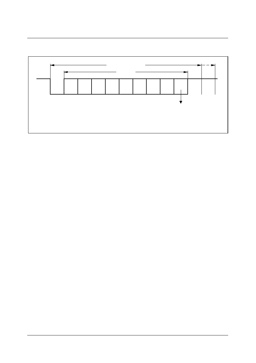
SDA 6000 / SDA 6001
PRELIMINARY DATA SHEET
Version 3.00
Peripherals
7 - 53
Micronas
Figure 7-26 Asynchronous 9-Bit Frames
In wake-up mode, received frames are only transferred to the receive buffer register if
the 9th bit (the wake-up bit) is `1'. If this bit is `0', no receive interrupt request will be
activated and no data will be transferred.
This feature may be used to control communication in a multi-processor system:
When the master processor wants to transmit a block of data to one of several slaves, it
first sends out an address byte which identifies the target slave. An address byte differs
from a data byte in that the additional 9th bit is a `1' for an address byte and a `0' for a
data byte, so no slave will be interrupted by a data `byte'. An address `byte' will interrupt
all slaves (operating in 8-bit data + wake-up bit mode), so each slave can examine the 8
LSBs of the received character (the address). The addressed slave will switch to 9-bit
data mode (e.g. by clearing bit S0M.0), which enables it to also receive further data bytes
(having the wake-up bit cleared). The slaves that were not being addressed remain in 8-
bit data + wake-up bit mode, ignoring the following data bytes.
IrDA Frames
The modulation schemes of IrDA is based on standard asynchronous data transmission
frames. The asynchronous data format in IrDA mode (S0M = 010
B
) is defined as follows:
� 1 start bit/8 data bits/1 stop bit
The coding/decoding of/to the asynchronous data frames is shown in Figure 7-27. In
general, during the IrDA transmissions, UART frames are encoded into IR frames and
vice versa. A low level on the IR frame indicates a `LED off' state. A high level on the IR
frame indicates a `LED on' state.
For a `0'-bit in the UART frame, a high pulse is generated. For a `1'-bit in the UART frame,
no pulse is generated. The high pulse starts in the middle of a bit cell and has a fixed
width of 3/16 of the bit time. The ASC0 also allows the length of the IrDA high pulse to
be programmed. Furthermore, the polarity of the received IrDA pulse can be inverted in
IrDA mode. Figure 7-27 shows the non-inverted IrDA pulse scheme.
UED11145
0
Bit
Start
LSB
D0
D1
D2
D3
D4
D5
D6
D7
Bit 9
(1st)
Stop
Bit
(2nd)
Bit
Stop
1
1
9 Data Bits
11-/12-Bit UART Frame
SOM = 100
SOM = 101
SOM = 111
B
B
B
: Bit 9 = Parity Bit
: Bit 9 = Wake-up Bit
: Bit 9 = Data Bit D8
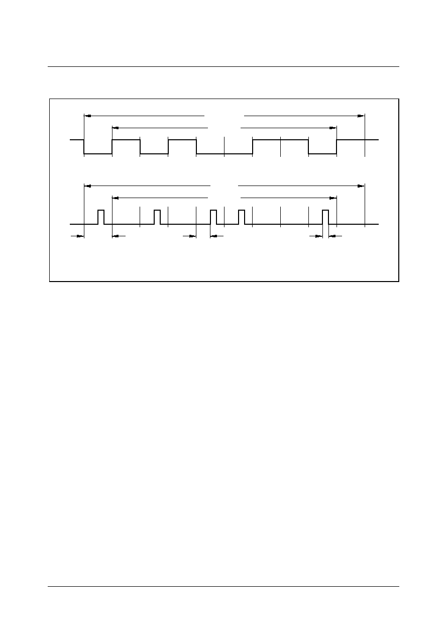
SDA 6000 / SDA 6001
PRELIMINARY DATA SHEET
Version 3.00
Peripherals
7 - 54
Micronas
Figure 7-27 IrDA Frame Encoding/Decoding
7.3.1.2
Asynchronous Transmission
Asynchronous transmission begins at the next overflow of the divide-by-16 baud rate
timer (transition of the baud rate clock
f
BR
), if bit S0R must be set and data has been
loaded into S0TBUF. The transmitted data frame consists of three basic elements:
� the start bit
� the data field (8 or 9 bits, LSB first, including a parity bit, if selected)
� the delimiter (1 or 2 stop bits)
Data transmission is double buffered. When the transmitter is idle, the transmit data
loaded into S0TBUF is immediately moved to the transmit shift register thus freeing
S0TBUF for the next data to be sent. This is indicated by the transmit buffer interrupt
request line S0TBIR being activated. S0TBUF may now be loaded with the next data,
while transmission of the previous one is still going on.
The transmit interrupt request line S0TIR will be activated before the last bit of a frame
is transmitted, e.g. before the first or the second stop bit is shifted out of the transmit shift
register.
For alternate data output the transmitter output pin TXD0 must be configured.
UED11146
8 Data Bits
0
1
1
0
0
0
1
1
0
1
UART Frame
Bit
Start
Stop
Bit
0
0
1
0
1
0
1
1
0
1
IR Frame
Bit
Start
8 Data Bits
Stop
Bit
Bit Time
1/2 BitTime
Pulse Width =
3/16 Bit Time
(or variable length)

SDA 6000 / SDA 6001
PRELIMINARY DATA SHEET
Version 3.00
Peripherals
7 - 55
Micronas
7.3.1.3
Asynchronous Reception
Asynchronous reception is initiated by a falling edge (1-to-0 transition) on pin RXD0,
provided that bits S0R and S0REN are set. The receive data input pin RXD0 is sampled
at 16 times the rate of the selected baud rate. A majority decision of the 7th, 8th and 9th
sample determines the effective bit value. This avoids erroneous results that may be
caused by noise.
If the detected value is not equal to `0' when the start bit is sampled, the receive circuit
is reset and waits for the next 1-to-0 transition at pin RXD0. If the start bit proves valid,
the receive circuit continues sampling and shifts the incoming data frame into the receive
shift register.
When the last stop bit has been received, the content of the receive shift register is
transferred to the receive data buffer register S0RBUF. Simultaneously, the receive
interrupt request line S0RIR is activated after the 9th sample in the last stop bit time slot
(as programmed), regardless whether valid stop bits have been received or not. The
receive circuit then waits for the next start bit (1-to-0 transition) at the receive data input
pin.
The receiver input pin RXD0 must be configured for input.
Asynchronous reception is stopped by clearing bit S0REN. A currently received frame is
completed including the generation of the receive interrupt request and an error interrupt
request, if appropriate. Start bits that follow this frame will not be recognized.
Note: In wake-up mode received frames are only transferred to the receive buffer
register, if the 9th bit (the wake-up bit) is equal to `1'. If this bit is equal to `0', no
receive interrupt request will be activated and no data transferred.
IrDA Mode
The duration of the IrDA pulse is normally 3/16 of a bit period. The IrDA standard also
allows the pulse duration to be independent of the baud rate or bit period. In this case
the transmitted pulse always has the width corresponding to the 3/16 pulse width at
115.2 KBaud which is 1.67
�
s. Both bit period dependent or fixed IrDA pulse width
generation can be selected. The IrDA pulse width mode is selected by bit S0IRPW,
which is located in register S0PWM.
In case of a fixed IrDA pulse width generation, the lower 8 bits in register S0PWM are
used to adapt the IrDA pulse width to a fixed value of e.g. 1.67
�
s. The fixed IrDA pulse
width is generated by a programmable timer as shown in Figure 7-28.
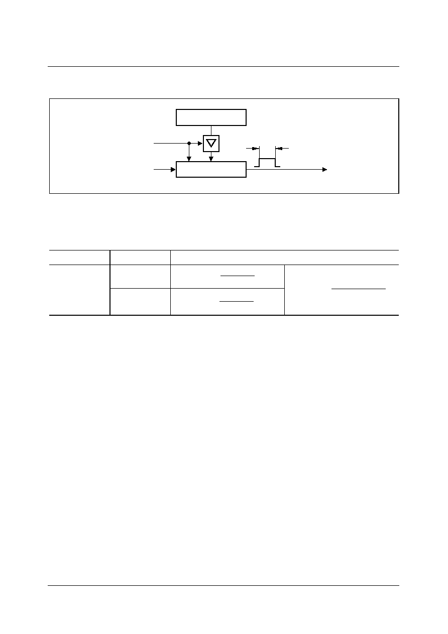
SDA 6000 / SDA 6001
PRELIMINARY DATA SHEET
Version 3.00
Peripherals
7 - 56
Micronas
Figure 7-28 Fixed IrDA Pulse Generation
The IrDA pulse width can be calculated according to the formulas given in the following
table.
The name S0PWM in the formulas represents the contents of the reload register
S0PWM (bits S0PW0-7), taken as an unsigned 8-bit integer.
The content of S0PWM further defines the minimum IrDA pulse width (
t
IPW min
) which is
still recognized as a valid IrDA pulse during a receive operation. This function is
independent of the selected IrDA pulse width mode (fixed or variable) which is defined
by bit S0IRPW in register S0PWM. The minimum IrDA pulse width is calculated by a shift
right operation of S0PWM bit 7-0 by one bit divided by the CPU clock (33.33 MHz).
Note: If S0IRPW=0 (fixed IrDA pulse width), SxPWM bit 7-0 must be loaded with a value
which assures that
t
IPW
>
t
IPW min
.
RXD/TXD Data Path Selection in Asynchronous Modes
The data paths for the serial input and output data in asynchronous modes are affected
by several control bits in the registers S0CON and S0ABCON, as shown in Figure 7-29.
The synchronous mode operation is not affected by these data path selection
capabilities.
The input signal from RXD passes an inverter which is controlled by bit ABCON_RXINV.
The output signal of this inverter is used for the autobaud detection and may bypass the
ASC_P logic in the echo mode (controlled by bit ABCON_ABEM). Furthermore, two
multiplexers are in the RXD input signal path to provide the loopback mode capability
(controlled by bit CON_LB) and the IrDA receive pulse inversion capability (controlled by
bit CON_RXDI).
S0PWM
S0IPWM
Formulas
1 ... 255
0
1
UED11147
S0PWM
8-Bit Timer
33 MHz
Start Timer
IPW
t
IrDA Pulse
t
IPW
=
16 x 33 MHz
3
t
IPW min
=
33 MHz
(S0PWM >> 1)
t
IPW
=
33 MHz
S0PWM
SDA 6000 / SDA 6001
PRELIMINARY DATA SHEET
Version 3.00
Peripherals
7 - 57
Micronas
Depending on the asynchronous operating mode (controlled by bitfield CON_M), the
ASC output signal or the RXD input signal in echo mode (controlled by bit
ABCON_ABEM) is switched to the TXD output by an inverter (controlled by bit
ABCON_TXINV).
Figure 7-29 RXD/TXD Data Path in Asynchronous Modes
In echo mode, the transmit output signal of the ASC_P3 logic is blocked by the echo
mode output multiplexer. Figure 7-29 also shows that it is not possible to use an IrDA
coded receiver input signal for autobaud detection.
7.3.2
Synchronous Operation
Synchronous mode supports half-duplex communication, basically for simple I/O
expansion via shift registers. Data is transmitted and received via pin RXD0 while pin
TXD0 outputs the shift clock. These signals are alternate functions of port pins.
Synchronous mode is selected with S0M = `000
B
'.
8 data bits are transmitted or received synchronous to a shift clock, generated by the
internal baud rate generator. The shift clock is only active as long as data bits are
transmitted or received.
UED11148
MUX
RxD
MUX
MUX
Coding
IrDA
Decoding
IrDA
Asynch. Mode Logic
ASC
CON
LB
RxDI
MUX
MUX
MUX
TxD
Detection
ABCON
Autobaud
RXINV
TXINV
ABEM
M
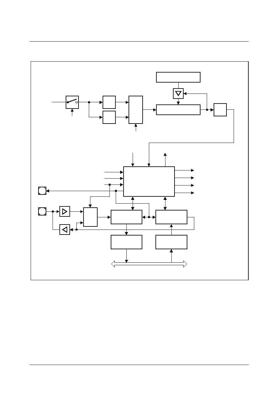
SDA 6000 / SDA 6001
PRELIMINARY DATA SHEET
Version 3.00
Peripherals
7 - 58
Micronas
Figure 7-30 Synchronous Mode of Serial Channel ASC0
7.3.2.1
Synchronous Transmission
Synchronous transmission begins within 4 state times after data has been loaded into
S0TBUF, provided that S0R is set and S0REN = `0' (half-duplex, no reception).
Exception: in loop-back mode (bit S0LB in S0CON set), S0REN must be set to receive
the transmitted byte. Data transmission is double buffered. When the transmitter is idle,
the transmit data loaded into S0TBUF is immediately moved to the transmit shift register
thus freeing S0TBUF for the next data to be sent. This is indicated by the transmit buffer
interrupt request line S0TBIR being activated. S0TBUF may now be loaded with the next
UES11149
13-Bit Reload Register
13-Bit Baud Rate Timer
4
�
f
BR
DIV
f
3
�
2
�
MUX
S0BRS
S0R
33 MHz
Serial Port Control
Shift Clock
Shift Clock
S0REN
S0LB
S0OEN
S0RIR
S0EIR
S0TIR
S0TBIR
Receive Int. Request
Transmit Int. Request
Transmit Buffer Int. Request
Error Int. Request
S0M = 000
S0OE
Transmit Shift
Register
Transmit Buffer
Reg. S0TBUF
Receive Buffer
Register
Receive Shift
Reg. S0RBUF
Internal Bus
f
BRT
B
MUX
0
1
TxD0
RxD0

SDA 6000 / SDA 6001
PRELIMINARY DATA SHEET
Version 3.00
Peripherals
7 - 59
Micronas
data, while transmission of the previous one is still going on. The data bits are
transmitted synchronous to the shift clock. After the bit time for the 8th data bit, both pins
TXD0 and RXD0 will go high, the transmit interrupt request line S0TIR is activated, and
serial data transmission stops.
Pin TXD0 must be configured for alternate data output in order to support the shift clock.
Pin RXD0 must also be configured for output during transmission.
7.3.2.2
Synchronous Reception
Synchronous reception is initiated by setting bit S0REN = `1'. If bit S0R = 1, the data
applied at pin RXD0 is clocked into the receive shift register synchronous to the clock
which is output at pin TXD0. After the 8th bit has been moved in, the content of the
receive shift register is transferred to the receive data buffer S0RBUF, the receive
interrupt request line S0RIR is activated, the receiver enable bit S0REN is reset, and
serial data reception stops.
Pin TXD0 must be configured for alternate data output in order to support the shift clock.
Pin RXD0 must be configured as an alternate data input.
Synchronous reception is terminated by clearing bit S0REN. A currently received byte is
completed including the generation of the receive interrupt request and an error interrupt
request, if appropriate. Writing to the transmit buffer register while a reception is in
progress has no effect on reception and will not start a transmission.
If a previously received byte has not been read out of the receive buffer register at the
time the reception of the next byte is complete, both the error interrupt request line S0EIR
and the overrun error status flag S0OE will be activated/set, provided the overrun check
has been enabled by bit S0OEN.
7.3.2.3
Synchronous Timing
Figure 7-31 shows timing diagrams of the ASC0 synchronous mode data reception and
data transmission. In idle state the shift clock is at high level. With the beginning of a
synchronous transmission of a data byte, the data is shifted out at pin RXD0 with the
falling edge of the shift clock. If a data byte is received through pin RXD0, data is latched
with the rising edge of the shift clock.
Between two consecutive receive or transmit data bytes one shift clock cycle (
f
BR
) delay
is inserted.
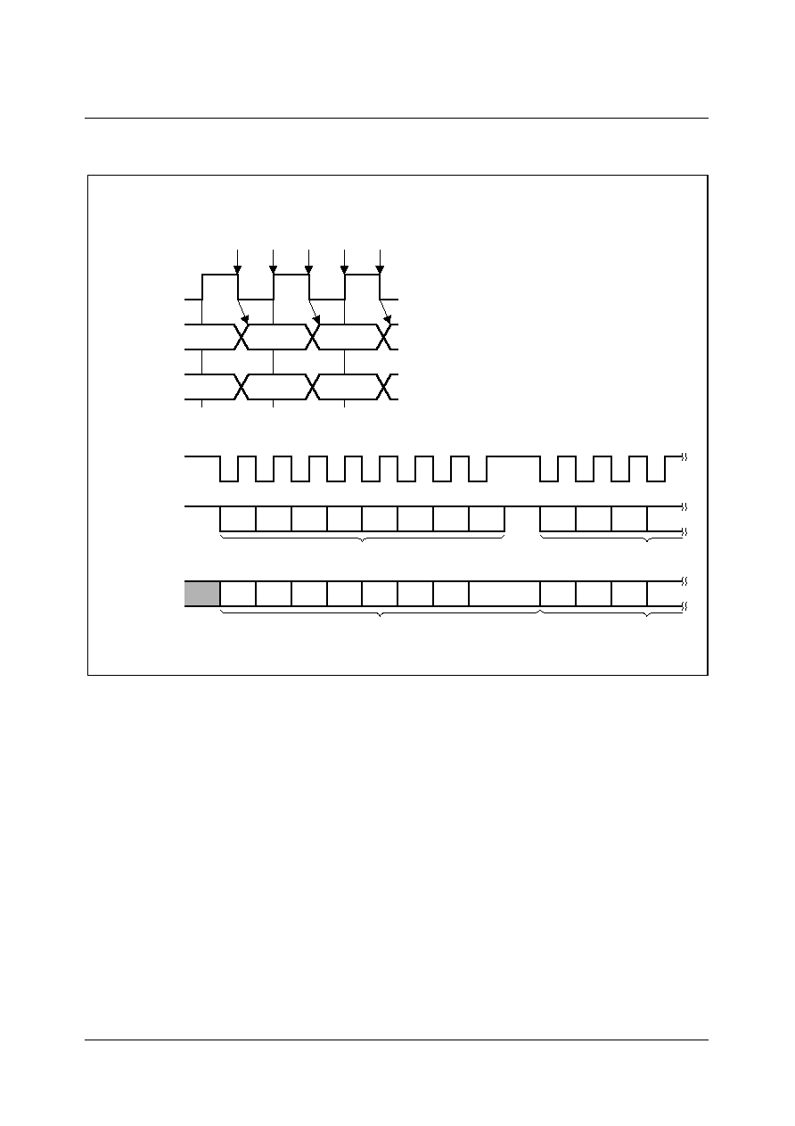
SDA 6000 / SDA 6001
PRELIMINARY DATA SHEET
Version 3.00
Peripherals
7 - 60
Micronas
Figure 7-31 ASC0 Synchronous Mode Waveforms
7.3.3
Baud Rate Generation
The serial channel ASC0 has its own dedicated 13-bit baud rate generator with 13-bit
reload capability, allowing baud rate generation to be independent of the GPT timers.
The baud rate generator is clocked with the CPU clock. The baud rate timer is counting
downwards and can be started or stopped through the baud rate generator run bit S0R
in register S0CON. Each underflow of the timer provides one clock pulse to the serial
channel. The timer is reloaded with the value stored in its 13-bit reload register each time
it underflows. The resulting clock
f
BRT
is again divided according to the operating mode
and controlled by the baud rate selection bit S0BRS. If S0BRS = `1', the clock signal is
additionally divided to 2/3rd of its frequency (see formulas and table). So the baud rate
of ASC0 is determined by the CPU clock, the reload value, the value of S0BRS and the
operating mode (asynchronous or synchronous).
UET11150
Receive Data
D0
D1
D2
D3
D4
D5
D6
D7
D0
D1
D2
D3
1. Byte
2. Byte
Transmit Data
D1
D0
D2
D0
D6
1. Byte
D3
D4
D5
D7
D1
2. Byte
D2
D3
Shift Clock
Continuous Transmit Timing
Data Bit n+1
Data Bit n+2
Data Bit n
Shift Clock
Transmit Data
Valid Data n
Receive Data
Valid Data n+1
Valid Data n+2
Shift Latch Shift Latch Shift
Receive/Transmit Timing

SDA 6000 / SDA 6001
PRELIMINARY DATA SHEET
Version 3.00
Peripherals
7 - 61
Micronas
Register S0BG is the dual-function Baud Rate Generator/Reload register. Reading
S0BG returns the content of the timer (bits 15 ... 13 return zero), while writing to S0BG
always updates the reload register (bits 15 ... 13 are insignificant).
An auto-reload of the timer with the content of the reload register is performed each time
S0BG is written to. However, if S0R = `0' at the time the write operation to S0BG is
performed, the timer will not be reloaded until the first instruction cycle after S0R = `1'.
For a clean baud rate initialization, S0BG should only be written if S0R = `0'. If S0BG is
written with S0R = `1', an unpredicted behavior of the ASC0 may occur during the
running of transmit or receive operations.
7.3.3.1
Baud Rates in Asynchronous Mode
For asynchronous operation, the baud rate generator provides a clock
f
BRT
with 16 times
the rate of the established baud rate. Every received bit is sampled at the 7th, 8th and
9th cycle of this clock. The clock divider circuitry, which generates the input clock for the
13-bit baud rate timer, is extended by a fractional divider circuitry, which allows the
adjustment of more accurate baud rates and the extension of the baud rate range.
The baud rate of the baud rate generator depends on the following bits and register
values:
� CPU clock
� Selection of the baud rate timer input clock
f
DIV
by bits S0FDE and S0BRS
� If bit S0FDE = 1 (fractional divider): value of register S0FDV
� Value of the 13-bit reload register S0BG
The output clock of the baud rate timer with the reload register is the sample clock in the
asynchronous modes of the ASC0. For baud rate calculations, this baud rate clock
f
BR
is
derived from the sample clock
f
DIV
by a division of 16.

SDA 6000 / SDA 6001
PRELIMINARY DATA SHEET
Version 3.00
Peripherals
7 - 62
Micronas
Figure 7-32 ASC0 Baud Rate Generator Circuitry in Asynchronous Modes
Using the fixed Input Clock Divider
The baud rate for asynchronous operation of serial channel ASC0, when using the fixed
input clock divider ratios (S0FDE = 0) and the required reload value for a given baud
rate, can be determined by the following formulas:
S0BG represents the content of the reload register S0BG, taken as an unsigned 13-bit
integer.
The maximum baud rate that can be achieved by the asynchronous modes when using
the two fixed clock dividers and a CPU clock of 33.33 MHz is 1041.66 KBaud. The table
S0FDE
S0BRS
S0BG
Formula
0
0
0 ... 8191
1
UES11151
13-Bit Reload Register
13-Bit Baud Rate Timer
16
�
f
BR
DIV
f
3
�
2
�
Fractional
Divider
MUX
S0FDE
S0BRS
S0R
33 MHz
f
BRT
Baud Rate
Clock
Sample
Clock
S0FDE
S0BRS
Selected Divider
0
0
1
X
1
0
� 2
� 3
Fractional Divider
32 x (S0BG+1)
Baud rate =
33 MHz
32 x Baud rate
33 MHz
S0BG =
- 1
48 x (S0BG+1)
Baud rate =
33 MHz
48 x Baud rate
33 MHz
S0BG =
- 1
SDA 6000 / SDA 6001
PRELIMINARY DATA SHEET
Version 3.00
Peripherals
7 - 63
Micronas
below lists various commonly used baud rates, together with the required reload values
and the deviation errors compared to the intended baud rate.
Note: S0FDE must be equal to 0 to achieve the baud rates in the table above. The
deviation errors given in the table are rounded. Using a baud rate crystal will
provide correct baud rates without deviation errors.
Using the Fractional Divider
When the fractional divider is selected, the input clock
f
DIV
for the baud rate timer is
derived from the CPU clock by a programmable divider. If S0FDE = 1, the fractional
divider is activated, It divides 33.33 MHz by a fraction of n/512 for any value of n from 0
to 511. If n = 0, the divider ratio is 1 which means that
f
DIV
= 33.33 MHz.
S0BG represents the content of the reload register S0BG, taken as an unsigned 13-bit
integer.
S0FDV represents the content of the fractional divider register taken as an unsigned 9-
bit integer.
Baud Rate
S0BRS = `0',
f
MOD
= 33.33 MHz
S0BRS = `1',
f
MOD
= 33.33 MHz
Deviation Error Reload Value
Deviation Error Reload Value
1041.66 KBaud
�
0000
H
�
�
694.4 KBaud
�
�
�
0000
H
19.2 KBaud
+ 0.4%/� 1.3%
0035
H
/0036
H
+ 0.5%/� 2.2%
0023
H
/0024
H
9600 Baud
+ 0.4%/� 0.4%
006b
H
/006C
H
+ 0.5%/� 0.9%
0047
H
/0048
H
4800 Baud
+ 0.0%/� 0.4%
00D8
H
/00D9
H
+ 0.5%/� 0.2%
008F
H
/0090
H
2400 Baud
+ 0.0%/� 0.2%
01B1
H
/01B2
H
+ 0.1%/� 0.2%
0120
H
/0121
H
1200 Baud
+ 0.0%/� 0.1%
0363
H
/0364
H
+ 0.1%/� 0.0%
0241
H
/0242
H
110 Baud
+ 0.0%/� 0.0%
24FC
H
/24FD
H
+ 0.0%/� 0.0%
18A8
H
/18A9
H
S0FDE
S0BRS
S0BG
S0FDV
Formula
1
�
1 ... 8191 1 ... 511
0
S0FDV
16 x (S0BG+1)
Baud rate =
33MHz
512
x
16 x (S0BG+1)
Baud rate =
33MHz
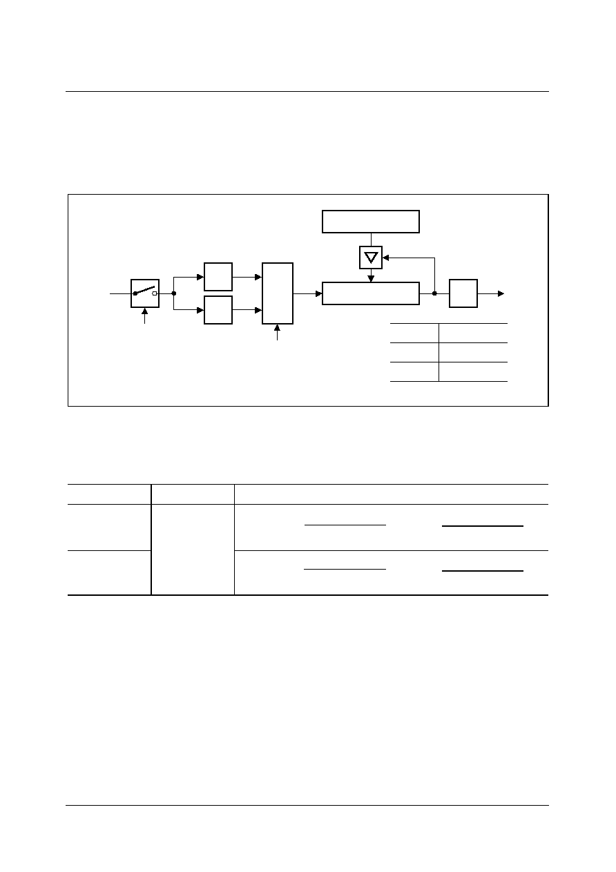
SDA 6000 / SDA 6001
PRELIMINARY DATA SHEET
Version 3.00
Peripherals
7 - 64
Micronas
7.3.3.2
Baud Rates in Synchronous Mode
For synchronous operation, the baud rate generator provides a clock with 4 times the
rate of the established baud rate (see Figure 7-33).
Figure 7-33 ASC0 Baud Rate Generator Circuitry in Synchronous Mode
The baud rate for synchronous operation of serial channel ASC0 can be determined by
the formulas as shown in the following table.
S0BG represents the content of the reload register, taken as unsigned 13-bit integers.
The maximum baud rate that can be achieved in synchronous mode when using a CPU
clock of 33.33 MHz is 4.166 MBaud.
7.3.4
Autobaud Detection
The autobaud detection unit provides an ability to recognize the mode and the baud rate
of an asynchronous input signal at RXD. Generally, the baud rates to be recognized
should be known by the application. With this knowledge, a set of nine baud rates can
always be detected. The autobaud detection unit is not designed to calculate a baud rate
of an unknown asynchronous frame.
S0BRS
S0BG
Formula
0
0 ... 8191
1
UES11152
13-Bit Reload Register
13-Bit Baud Rate Timer
4
�
f
BR
DIV
f
3
�
2
�
MUX
S0BRS
S0R
33 MHz
f
BRT
Sample
Clock
S0BRS
Selected Divider
1
0
� 2
� 3
Shift/
8 x (S0BG+1)
Baud rate =
33 MHz
8 x Baud rate
33 MHz
S0BG =
- 1
12 x (S0BG+1)
Baud rate =
33 MHz
12 x Baud rate
33MHz
S0BG =
- 1

SDA 6000 / SDA 6001
PRELIMINARY DATA SHEET
Version 3.00
Peripherals
7 - 65
Micronas
Figure 7-34 shows how the autobaud detection unit of the ASC is integrated into its
asynchronous mode configuration. The RXD data line is an input of the autobaud
detection unit. The clock
f
DIV
, which is generated by the fractional divider, is used by the
autobaud detection unit as a time base. After successful recognition of the baud rate and
asynchronous operating mode of the RXD data input signal, bits in the CON register and
the value of the BG register in the baud rate timer are set to the appropriate values, and
the ASC_P3 can start immediately with the reception of serial input data.
Figure 7-34 ASC_P3 Asynchronous Mode Block Diagram
The following sequence must be generally executed to start the operation of the
autobaud detection unit:
� Definition of the baud rates to be detected: standard or non-standard baud rates
� Programming of the Prescaler/Fractional Divider to select a specific value of
f
DIV
� Starting the Prescaler/Fractional Divider (setting CON_R)
� Preparing the interrupt system of the CPU
� Enabling the autobaud detection (setting ABCON_ EN and the interrupt enable bits in
ABCON for interrupt generation, if required)
� Polling interrupt request flag or waiting for the autobaud detection interrupt
7.3.4.1
Serial Frames for Autobaud Detection
The autobaud detection of the ASC_P3 is based on the serial reception of a specific two-
byte serial frame. This serial frame is build up by the two ASCII bytes `at' or `AT' (`aT' or
`At' are not allowed). Both byte combinations can be detected in five types of
asynchronous frames. Figure 7-35 and Figure 7-36 show the serial frames which are
least detected.
UEB11153
Receive/Transmit
Buffers and
Shift Registers
Serial Port
Control
Baud Rate
Timer
Prescaler/
Fractional Divider
Detection
Autobaud
DIV
f
f
MOD
Coding
IrDA
MUX
Decoding
IrDA
MUX
TxD
RxD
Asynchronous Mode
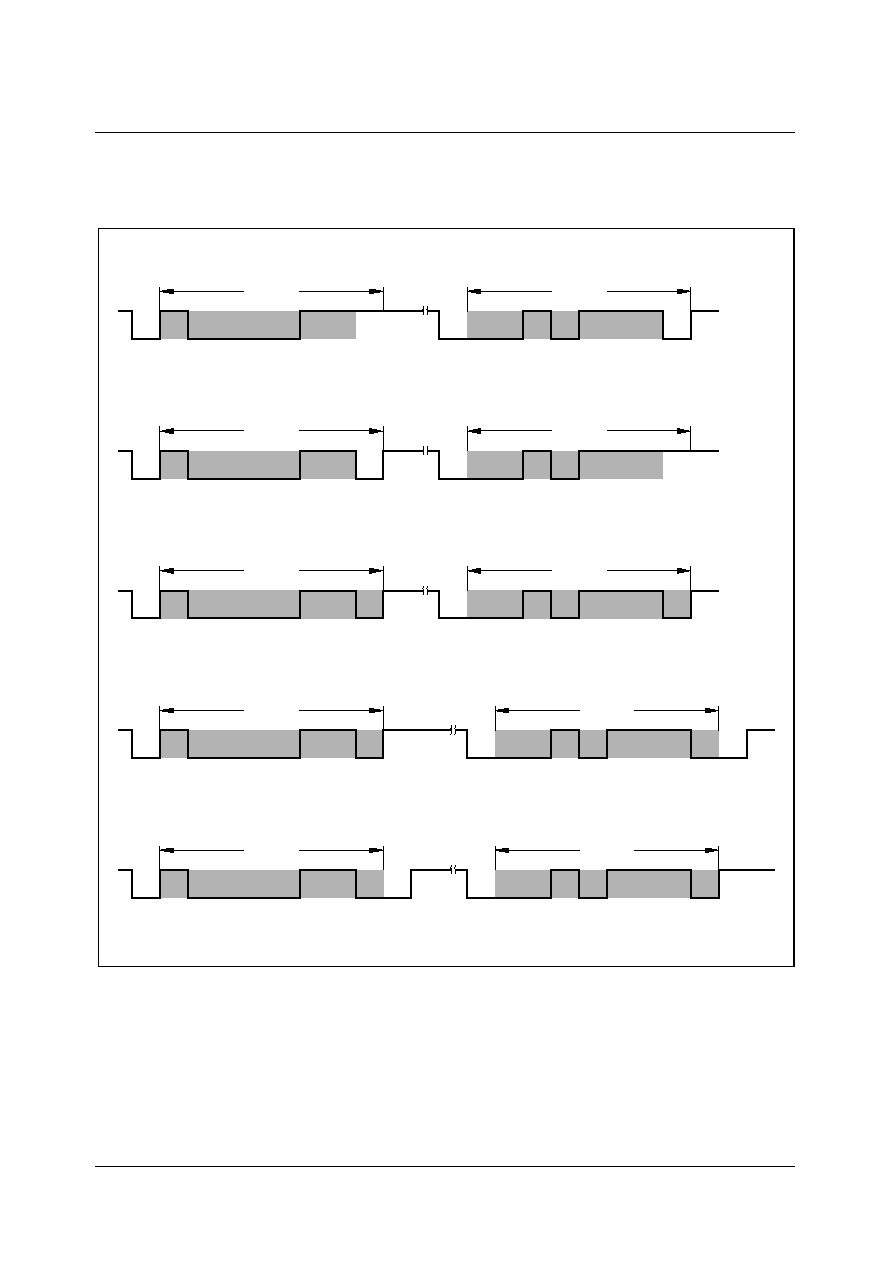
SDA 6000 / SDA 6001
PRELIMINARY DATA SHEET
Version 3.00
Peripherals
7 - 66
Micronas
Note: Some other two-byte combinations will also be defined.
Figure 7-35 Two-Byte Serial Frames with ASCII `at'
1
1
1
0
0
0
0
0
1
1
1
1
0
1
0
1
0
0
0
8 Bit, Odd Parity
Start
1
0
0
0
1
'a' = 61
H
0
8 Bit, Even Parity
Start
1
Start
'a' = 61
0
0
1
0
H
1
1
Parity Stop
1
0
0
1
Start
0
0
Start
Parity Stop
1
0
1
1
Stop
Start
0
0
0
1
1
1
H
't' = 74
UED11154
Parity Stop
0
1
1
H
1
0
't' = 74
1
1
Parity Stop
0
0
1
Stop
'a' = 61
0
8 Bit, No Parity
Start
1
'a' = 61
H
0
0
0
H
1
0
7 Bit, Odd Parity
7 Bit, Even Parity
Start
1
'a' = 61
0
0
H
0
1
0
't' = 74
0
't' = 74
't' = 74
Start
Parity Stop
1
0
1
0
0
1
Start
Parity Stop
1
1
1
0
0
1
Parity Stop
H
H
1
1
1
1
1
Parity Stop
H
1
1
1
0
1
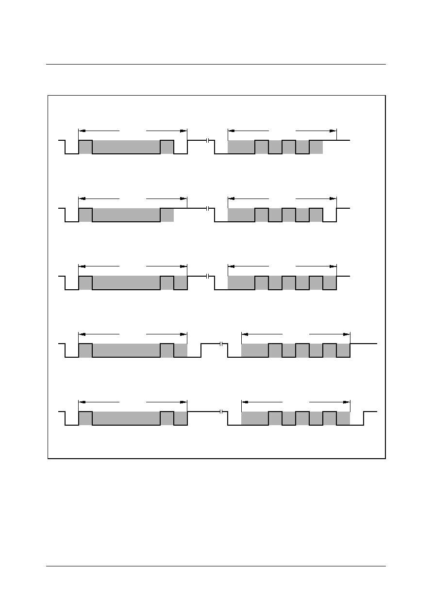
SDA 6000 / SDA 6001
PRELIMINARY DATA SHEET
Version 3.00
Peripherals
7 - 67
Micronas
Figure 7-36 Two-Byte Serial Frames with ASCII `AT'
1
1
0
0
0
0
0
0
1
1
1
0
1
0
0
1
0
0
0
8 Bit, Odd Parity
Start
1
0
0
0
0
'A' = 41
H
0
8 Bit, Even Parity
Start
1
Start
'A' = 41
0
0
0
0
H
1
1
Parity Stop
1
0
1
1
Start
0
0
Start
Parity Stop
1
0
0
1
Stop
Start
0
0
0
1
0
1
H
'T' = 54
UED11155
Parity Stop
0
0
1
H
1
0
'T' = 54
1
0
Parity Stop
1
0
1
Stop
'A' = 41
0
8 Bit, No Parity
Start
1
'A' = 41
H
0
0
H
0
0
0
7 Bit, Odd Parity
7 Bit, Even Parity
Start
1
'A' = 41
0
0
H
0
0
0
'T' = 54
0
'T' = 54
'T' = 54
Start
Parity Stop
1
1
1
0
0
1
Start
Parity Stop
1
0
1
0
0
1
Parity Stop
H
1
0
H
1
0
1
Parity Stop
H
1
0
1
1
1

SDA 6000 / SDA 6001
PRELIMINARY DATA SHEET
Version 3.00
Peripherals
7 - 68
Micronas
7.3.4.2
Baud Rate Selection and Calculation
The autobaud detection requires some calculations concerning the programming of the
baud rate generator and the baud rates to be detected. Two steps must be considered:
� Defining the baud rate(s) to be detected
� Programming of the baud rate timer prescaler - setup of the clock rate of
f
DIV
In general, the baud rate generator of the ASC in asynchronous mode is built up of two
parts:
� the clock prescaler part which derives
f
DIV
from
f
MOD
� the baud rate timer part which generates the sample clock
f
BRT
and the baud rate clock
f
BR
Prior to an autobaud detection, the prescaler part has to be set up by the CPU while the
baud rate timer (register BG) is automatically initialized with a 13-bit value (BR_VALUE)
after a successfull autobaud detection. For the subsequent calculations, the fractional
divider is used (CON_FDE = 1).
Note: It is also possible to use the fixed divide-by-2 or divide-by-3 prescaler. But the
fractional divider allows for a more precise adaption of
f
DIV
to the required value.
Standard Baud Rates
For standard baud rate detection the baud rates as shown in Table 7-20 can be
detected. Therefore, the output frequency
f
DIV
of the ASC baud rate generator must be
set to a frequency derived from the system, clocked (33 MHz) in a way that it is equal to
11.0592 MHz. The value to be written into register FDV is the nearest integer value
which is calculated according the following formula:
Table 7-20 defines the nine standard baud rates (Br0 - Br8) which can be detected for
f
DIV
= 11.0592 MHz.
FDV =
512
�
11.0592 MHz
33 MHz
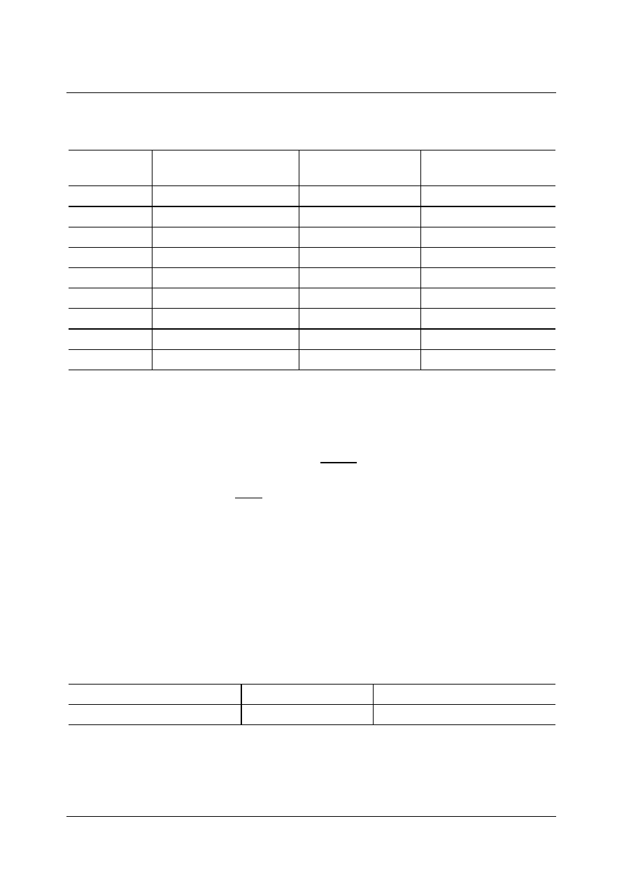
SDA 6000 / SDA 6001
PRELIMINARY DATA SHEET
Version 3.00
Peripherals
7 - 69
Micronas
According to Table 7-20 a baud rate of 9600 Baud is achieved when register BG is
loaded with a value of 047
H
, assuming that
f
DIV
has been set to 11.0592 MHz.
Table 7-20 also lists a divide factor d
f
which is defined with the following formula:
This divide factor d
f
defines a fixed relationship between the prescaler output frequency
f
DIV
and the baud rate to be detected during the autobaud detection operation. This
means, that changing
f
DIV
results in a totally different baud rate table in terms of baud
rate values. For the baud rates to be detected, the following relations are always valid:
� Br0 =
f
DIV
/48
D
, Br1 =
f
DIV
/96
D
,
...
up to Br8 =
f
DIV
/9216
D
,
A requirement for detecting standard baud rates up to 230.400 kBaud, is the f
DIV
minimum value of 11.0592 MHz. With the value FD_VALUE in register FDV, the
fractional divider f
DIV
is adapted to the system clock frequency 33 MHz. Table 7-21
defines the deviation of the standard baud rates when using autobaud detection
depending on the system
f
MOD
.
Note: If the deviation of the baud rate after autobaud detection is too high, the baud rate
generator (fractional divider FDV and reload register BG) can be reprogrammed if
required to get a more precise baud rate with less error.
Table 7-20
Autobaud Detection using Standard Baud Rates (
f
DIV
= 11.0592 MHz)
Baud Rate
Numbering
Detectable Standard
Baud Rate
Divide Factor d
f
BG is Loaded after
Detection with Value
Br0
230.400 kBaud
48
2
= 002
H
Br1
115.200 kBaud
96
5
= 005
H
Br2
57.600 kBaud
192
11 = 00B
H
Br3
38.400 kBaud
288
17 = 011
H
Br4
19.200 kBaud
576
35 = 023
H
Br5
9600 Baud
1152
71 = 047
H
Br6
4800 Baud
2304
143 = 08F
H
Br7
2400 Baud
4608
287 = 11F
H
Br8
1200 Baud
9216
575 = 23F
H
Table 7-21
Standard Baud Rates - Deviations and Errors for Autobaud Detection
f
MOD
FDV
Error in
f
DIV
33 MHz
172
+ 0.24%
baud rate =
f
DIV
d
f

SDA 6000 / SDA 6001
PRELIMINARY DATA SHEET
Version 3.00
Peripherals
7 - 70
Micronas
Non-Standard Baud Rates
Due to the relationship between Br0 to Br8 in Table 7-20 concerning the divide factor d
f
other baud rates than the standard ones can also be selected. For example, if a baud
rate of 50 kBaud has to be detected, Br2 is e.g. defined as baud rate for the 50 kBaud
detection. This further results in:
�
f
DIV
= 50 kBaud
�
d
f
@Br2 = 50 kBaud
�
192 = 9.6 MHz
Therefore, depending on the system clock frequency, the value of the fractional divider
(register FDV must be set according the formula in this example:
Using this selection (f
DIV
= 9.6 MHz), the detectable baud rates start at 200 kBaud (Br0)
down to 1042 Baud (Br8). Table 7-22 shows the baud rate table for this example.
7.3.4.3
Overwriting Registers on Successful Autobaud Detection
With a successful autobaud detection, some bits in register CON and BG are
automatically set to a value which corresponds to the mode and baud rate of the
detected serial frame conditions. In control register CON the mode control bits CON_M
and the parity select bit CON_ODD are overwritten. Register BG is loaded with the 13-
bit reload value for the baud rate timer.
Table 7-22
Autobaud Detection using Non-Standard Baud Rates (
f
DIV
= 9.6 MHz)
Baud Rate
Numbering
Detectable Non-
Standard Baud Rates
Divide Factor d
f
BG is Loaded after
Detection with Value
Br0
200.000 kBaud
48
2
= 002
H
Br1
100.000 kBaud
96
5
= 005
H
Br2
50 kBaud
192
11 = 00B
H
Br3
33.333 kBaud
288
17 = 011
H
Br4
16.667 kBaud
576
35 = 023
H
Br5
8333 Baud
1152
71 = 047
H
Br6
4167 Baud
2304
143 = 08F
H
Br7
2083 Baud
4608
287 = 11F
H
Br8
1047 Baud
9216
575 = 23F
H
FDV =
512 x
f
DIV
33 MHz
with
f
DIV
= 9.6 MHz

SDA 6000 / SDA 6001
PRELIMINARY DATA SHEET
Version 3.00
Peripherals
7 - 71
Micronas
7.3.5
ASC Hardware Error Detection Capabilities
To improve the safety of serial data exchange, the serial channel ASC0 provides an error
interrupt request flag, which indicates the presence of an error, and three (selectable)
error status flags in register S0CON, which indicate which error has been detected
during reception. Upon completion of a reception, the error interrupt request line S0EIR
will be activated simultaneously with the receive interrupt request line S0RIR if one or
more of the following conditions are met:
� The framing error detection enable bit S0FEN is set and any of the expected stop bits
are not high, the framing error flag S0FE is set, indicating that the error interrupt
request is due to a framing error (Asynchronous mode only).
� If the parity error detection enable bit S0PEN is set in the mode where a parity bit is
received, and the parity check on the received data bits proves false, the parity error
flag S0PE is set, indicating that the error interrupt request is due to a parity error
(Asynchronous mode only).
� If the overrun error detection enable bit S0OEN is set and the last character received
was not read out of the receive buffer by software or PEC transfer at the time the
reception of a new frame is complete, the overrun error flag S0OE is set, indicating
that the error interrupt request is due to an overrun error (Asynchronous and
synchronous mode).
Table 7-23
Autobaud Detection Overwrite Values for the CON Register
Detected Parameters
CON_M
CON_ODD BG_BR_VALUE
Operating Mode
7 bit, even parity
7 bit, odd parity
8 bit, even parity
8 bit, odd parity
8 bit, no parity
0 1 1
0 1 1
1 1 1
1 1 1
0 0 1
0
1
0
1
0
�
Baud rate
Br0
Br1
Br2
Br3
Br4
Br5
Br6
Br7
Br8
�
�
2 =
002
H
5
= 005
H
11 = 00B
H
17 = 011
H
35 = 023
H
71 = 047
H
143 = 08F
H
287 = 11F
H
575 = 23F
H

SDA 6000 / SDA 6001
PRELIMINARY DATA SHEET
Version 3.00
Peripherals
7 - 72
Micronas
7.3.6
Interrupts
Six interrupt sources are provided for serial channel ASC0. Line S0TIC indicates a
transmit interrupt, S0TBIC indicates a transmit buffer interrupt, S0RIC indicates a
receive interrupt and S0EIC indicates an error interrupt of the serial channel. The
autobaud detection unit provides two additional interrupts, the ABSTIR start of autobaud
operation interrupt and the ABDETIR autobaud detected interrupt. The interrupt output
lines S0TBIR, S0TIR, S0RIR, and S0EIR are activated (active state) for two periods of
the module clock
f
MOD
(33.33 MHz).
The cause of an error interrupt request (framing, parity, overrun error) can be identified
by the error status flags S0FE, S0PE, and S0OE which are located in control register
S0CON.
Note: In contrary to the error interrupt request line S0EIR, the error status flags S0FE/
S0PE/S0OE are not reset automatically but must be cleared by software.
For normal operation (e.g. besides the error interrupt) the ASC0 provides three interrupt
requests to control data exchange via this serial channel:
� S0TBIR is activated when data is moved from S0TBUF to the transmit shift register.
� S0TIR is activated before the last bit of an asynchronous frame is transmitted, or after
the last bit of a synchronous frame has been transmitted.
� S0RIR is activated when the received frame is moved to S0RBUF.
While the task of the receive interrupt handler is quite clear, the transmitter is serviced
by two interrupt handlers. This has its advantages for the servicing software.
For single transfers it is sufficient to use the transmitter interrupt (S0TIR), which indicates
that the previously loaded data, except for the last bit of an asynchronous frame, has
been transmitted.
For multiple back-to-back transfers it is necessary to wait to load the last piece of data
until the last bit of the previous frame has been transmitted. In asynchronous mode this
leaves just one bit-time for the handler to respond to the transmitter interrupt request, in
synchronous mode it is impossible.
Using the transmit buffer interrupt (S0TBIR) to reload transmitted data gives enough time
to transmit a complete frame for the service routine, as S0TBUF may be reloaded while
the previous data is still being transmitted.
The ABSTIR start of autobaud operation interrupt is generated whenever the autobaud
detection unit is enabled (ABEN, ABDETEN and ABSTEN set), and a start bit has been
detected at RXD. In this case ABSTIR is generated during autobaud detection whenever
a start bit is detected.
The ABDETIR autobaud detected interrupt is always generated after recognition of the
second character of the two-byte frame, after a successful autobaud detection. If
ABCON_FCDETEN is set the ABDETIR autobaud detected interrupt is also generated
after the recognition of the first character of the two-byte frame.
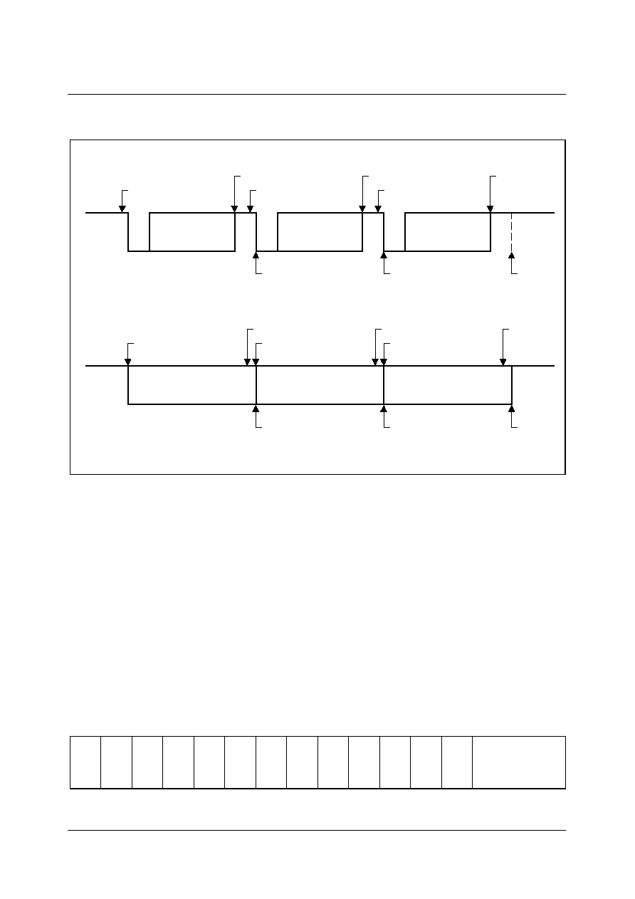
SDA 6000 / SDA 6001
PRELIMINARY DATA SHEET
Version 3.00
Peripherals
7 - 73
Micronas
Figure 7-37 ASC0 Interrupt Generation
As shown in Figure 7-37, S0TBIR is an early trigger for the reload routine, while S0TIR
indicates the completed transmission. Software using handshake therefore should rely
on S0TIR at the end of a data block to make sure that all data has really been
transmitted.
7.3.7
Register Description
The operating mode of the serial channel ASC0 is controlled by its control register
S0CON. This register contains control bits for mode and error check selection, and
status flags for error identification.
S0CON
Control Register
15
14
13
12
11
10
9
8
7
6
5
4
3
2
1
0
R
LB
BRS ODD FDE
OE
FE
PE
OEN FEN
PEN
/
RXD
I
REN STP
M
UED11156
Start
Idle
Start
Stop
Start
Stop
Stop
Idle
S0TBIR
S0TBIR
S0TBIR
S0TIR
S0TIR
S0TIR
S0RIR
S0RIR
S0RIR
Asynchronous Mode
S0RIR
S0TBIR
Synchronous Mode
Idle
S0TBIR
S0TIR
S0RIR
S0TBIR
S0TIR
S0RIR
S0TIR
Idle

SDA 6000 / SDA 6001
PRELIMINARY DATA SHEET
Version 3.00
Peripherals
7 - 74
Micronas
Field
Bits
Type
Value
Description
M
2-0
rwh
0 0 0
0 0 1
0 1 0
0 1 1
1 0 0
1 0 1
1 1 0
1 1 1
Mode Selection
8-bit data
sync. operation
8-bit data
async. operation
IrDA mode, 8-bit data
async. operation
7-bit data + parity
async. operation
9-bit data
async. operation
8-bit data + wake up bit async. operation
Reserved. Do not use this combination!
8-bit data + parity
async. operation
Bits are set/cleared by hardware after a
successful autobaud detection operation.
STP
3
rw
0
1
Number of Stop Bit Selection
One stop bit
Two stop bits
REN
4
rwh
0
1
Receiver Enable Control
Receiver disabled
Receiver enabled
Bit can be affected during autobaud
detection operation when bit
ABEN_AUREN is set.
Bit is reset by hardware after reception of
byte in synchronous mode.
PEN
RXDI
5
rw
0
1
0
1
Parity Check Enable/
IrDA Input Inverter Enable
All asynchronous modes without IrDA
mode:
Ignore parity
Check parity
Only in IrDA mode (M = 010):
RXD input is not inverted
RXD input is inverted
FEN
6
rw
0
1
Framing Check Enable
(async. modes only)
Ignore framing errors
Check framing errors
OEN
7
rw
0
1
Overrun Check Enable
Ignore overrun errors
Check overrun errors

SDA 6000 / SDA 6001
PRELIMINARY DATA SHEET
Version 3.00
Peripherals
7 - 75
Micronas
PE
8
rwh
�
Parity Error Flag
Set by hardware on a parity error
(PEN = `1'). Must be reset by software.
FE
9
rwh
�
Framing Error Flag
Set by hardware on a framing error
(FEN = `1'). Must be reset by software.
OE
10
rwh
�
Overrun Error Flag
Set by hardware on an overrun error
(OEN = `1'). Must be reset by software.
FDE
11
rw
0
1
Fractional Divider Enable
Fractional divider disabled
Fractional divider is enabled and used as
prescaler for baud rate timer (bit BRS is
don't care).
ODD
12
rwh
0
1
Parity Selection
Even parity selected (parity bit set on odd
number of `1's in data)
Odd parity selected (parity bit set on even
number of `1's in data)
Bit is be set/cleared by hardware after a
successful autobaud detection operation.
BRS
13
rw
0
1
Baud rate Selection
Baud rate timer prescaler divide-by-2
selected
Baud rate timer prescaler divide-by-3
selected
BRS is don't care if FDE = 1 (fractional
divider enabled)
LB
14
rw
0
1
Loop-back Mode Enable
Loop-back mode disabled
Loop-back mode enabled
R
15
rw
0
1
Baud rate Generator Run Control
Baud rate generator disabled (ASC_P
inactive)
Baud rate generator enabled
BG should only be written if R = `0'.
Field
Bits
Type
Value
Description
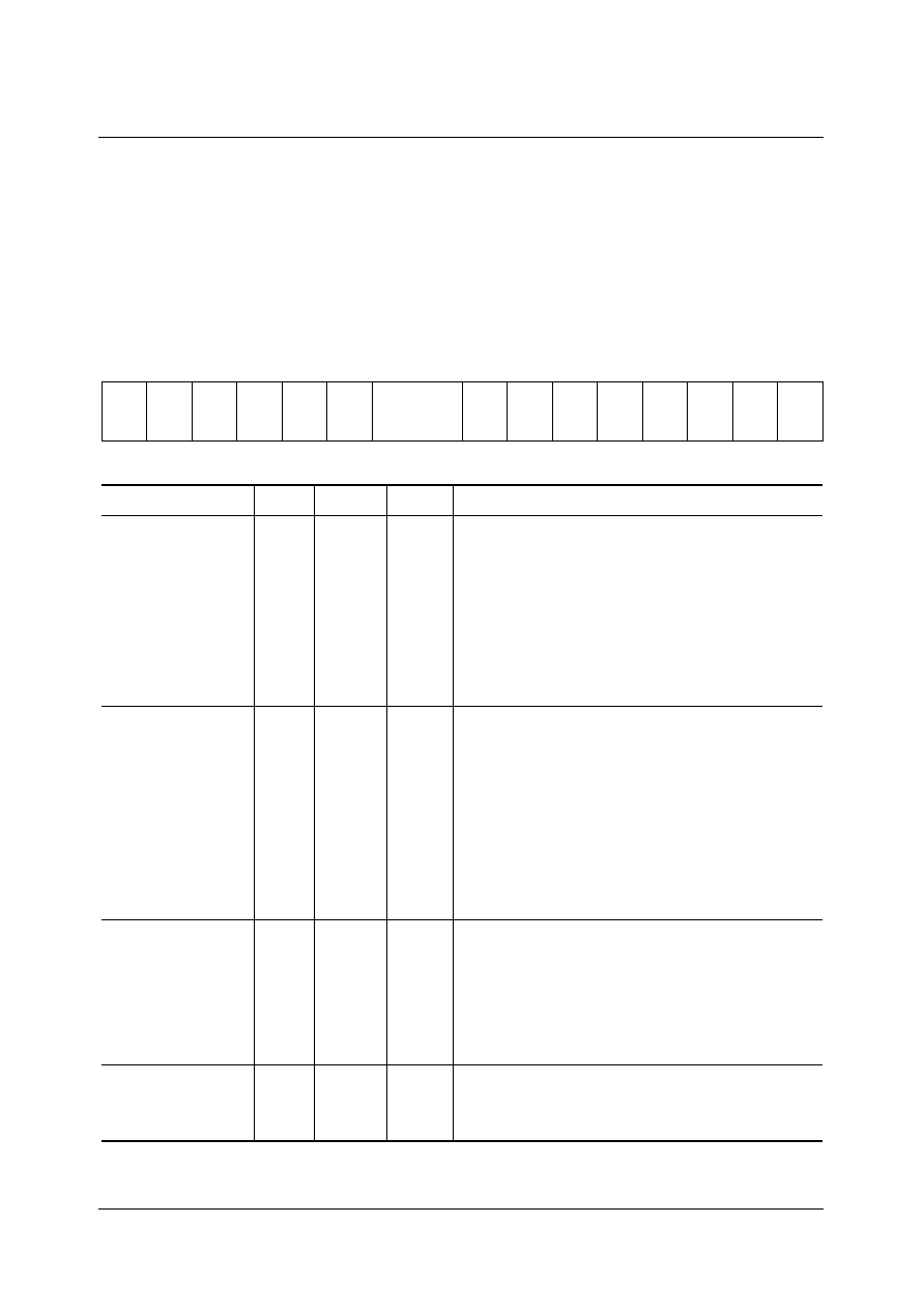
SDA 6000 / SDA 6001
PRELIMINARY DATA SHEET
Version 3.00
Peripherals
7 - 76
Micronas
The autobaud control register ABCON is used to control the autobaud detection
operation. It contains its general enable bit, the interrupt enable control bits, and data
path control bits
.
S0ABCON
Autobaud Control Register
15
14
13
12
11
10
9
8
7
6
5
4
3
2
1
0
0
0
0
0
RX
INV
TX
INV
ABEM
0
0
0
FC
DET
EN
AB
DET
EN
ABS
T
EN
AUR
EN
AB
EN
Field
Bits
Type
Value Description
ABEN
0
rwh
0
1
Autobaud Detection Enable
Autobaud detection is disabled
Autobaud detection is enabled
ABEN is reset by hardware after a
successful autobaud detection; (with the
stop bit detection of the second character).
Resetting ABEN by software if it was set
aborts the autobaud detection.
AUREN
1
rw
0
1
Automatic Autobaud Control of
CON_REN
CON_REN is not affected during autobaud
detection
CON_REN is cleared (receiver disabled)
when ABEN and AUREN are set together.
CON_REN is set (receiver enabled) after a
successful autobaud detection (with the
stop bit detection of the second character).
ABSTEN
2
rw
0
1
Start of Autobaud Detection Interrupt
Enable
Start of autobaud detection interrupt
disabled
Start of autobaud detection interrupt
enabled
ABDETEN
3
rw
0
1
Autobaud Detection Interrupt Enable
Autobaud detection interrupt disabled
Autobaud detection interrupt enabled

SDA 6000 / SDA 6001
PRELIMINARY DATA SHEET
Version 3.00
Peripherals
7 - 77
Micronas
The autobaud status register ABSTAT indicates the status of the autobaud detection
operation.
FCDETEN
4
rw
0
1
First Character of Two-Byte Frame
Detected Enable
Autobaud detection interrupt ABDETIR
becomes active after the two-byte frame
recognition
Autobaud detection interrupt ABDETIR
becomes active after detection of the first
and second byte of the two-byte frame.
ABEM
8-9
rw
0 0
0 1
1 0
1 1
Autobaud Echo Mode Enable
In echo mode the serial data at RXD is
switched to TXD output.
Echo mode disabled
Echo mode is enabled during autobaud
detection
Echo mode is always enabled
reserved
TXINV
10
rw
0
1
Transmit Inverter Enable
Transmit inverter disabled
Transmit inverter enabled
RXINV
11
rw
0
1
Receive Inverter Enable
Receive inverter disabled
Receive inverter enabled
Field
Bits
Type
Value Description

SDA 6000 / SDA 6001
PRELIMINARY DATA SHEET
Version 3.00
Peripherals
7 - 78
Micronas
S0ABSTAT
Autobaud Status Register
15
14
13
12
11
10
9
8
7
6
5
4
3
2
1
0
0
0
0
0
0
0
0
0
0
0
0
DET
WAI
T
SCC
DET
SCS
DET
FCC
DET
FCS
DET
Field
Bits
Type
Value
Description
FCSDET
0
rwh
0
1
First Character with Small Letter
Detected
no small `a' character detected
small `a' character detected
Bit is cleared by hardware when
ABCON_ABEN is set or if FCCDET or
SCSDET or SCCDET is set. Bit can be also
cleared by software.
FCCDET
1
rwh
0
1
First Character with Capital Letter
Detected
no capital `A' character detected
capital `A' character detected
Bit is cleared by hardware when
ABCON_ABEN is set or if FCSDET or
SCSDET or SCCDET is set. Bit can be also
cleared by software.
SCSDET
2
rwh
0
1
Second Character with Small Letter
Detected
no small `t' character detected
small `t' character detected
Bit is cleared by hardware when
ABCON_ABEN is set or if FCSDET or
FCCDET or SCCDET is set. Bit can be also
cleared by software.

SDA 6000 / SDA 6001
PRELIMINARY DATA SHEET
Version 3.00
Peripherals
7 - 79
Micronas
Note: SCSDET or SCCDET are set when the second character has been recognized.
CON_ABEN is reset, and ABDETIR set, after SCSDET or SCCDET have seen
set.
The baud rate timer reload register BG contains the 13-bit reload value for the baud rate
timer in asynchronous and sychronous mode.
SCCDET
3
rwh
0
1
Second Character with Capital Letter
Detected
no capital `T' character detected
capital `T' character detected
Bit is cleared by hardware when
ABCON_ABEN is set or if FCSDET or
FCCDET or SCSDET is set. Bit can be also
cleared by software.
DETWAIT
4
rwh
0
1
Autobaud Detection is Waiting
Either character `a', `A', `t', or `T' has been
detected.
The autobaud detection unit waits for the
first `a' or `A'
Bit is cleared when either FCSDET or
FCCDET is set (`a' or `A' detected). Bit can
be also cleared by software. DETWAIT is
set by hardware when ABCON_ABEN is
set.
Field
Bits
Type
Value
Description
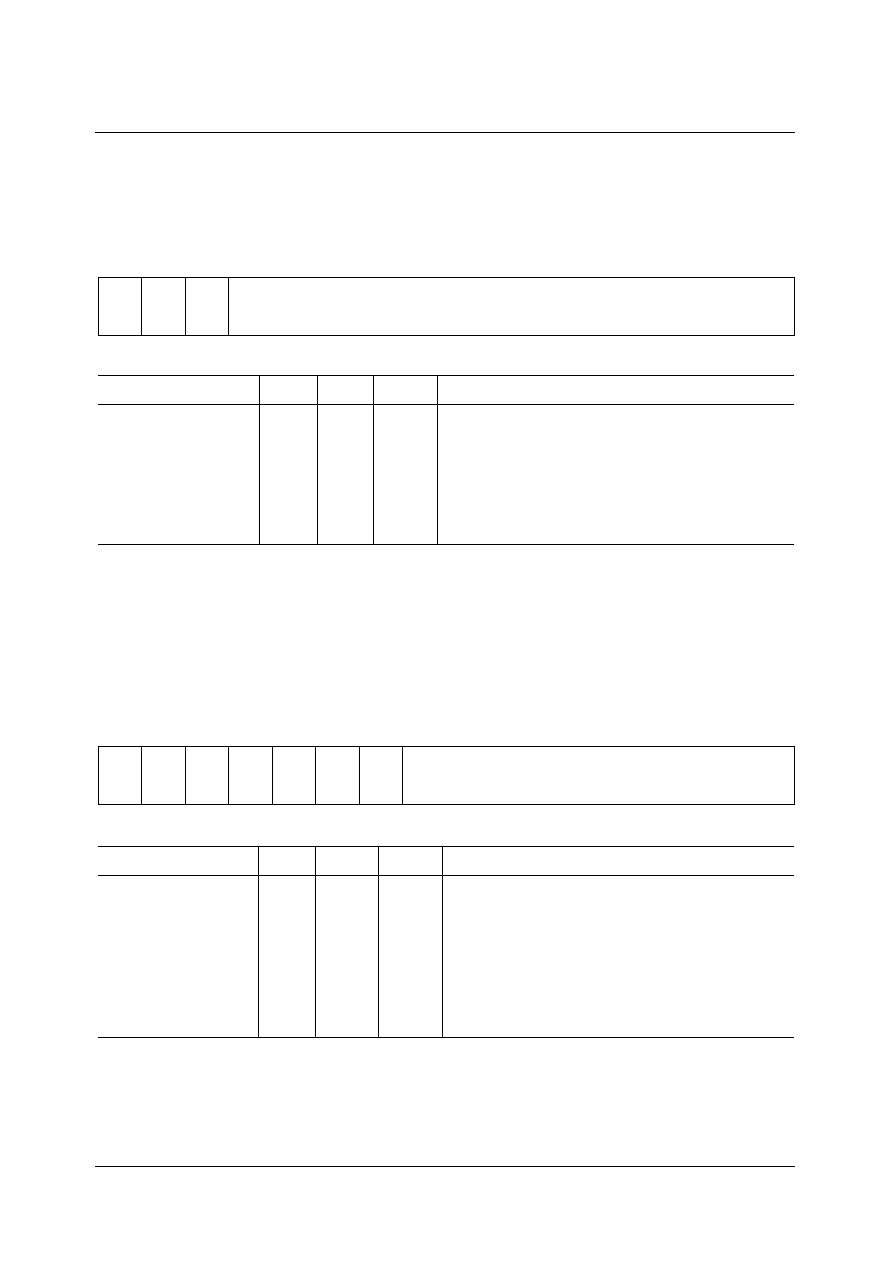
SDA 6000 / SDA 6001
PRELIMINARY DATA SHEET
Version 3.00
Peripherals
7 - 80
Micronas
The fractional divider register FDV contains the 9-bit divider value for the fractional
divider (asynchronous mode only). It is also used for reference clock generation of the
autobaud detection unit.
The IrDA pulse mode and width register PMW contains the 8-bit IrDA pulse width value
and the IrDA pulse width mode select bit. This register is only required in the IrDA
operating mode.
S0BG
Baud Rate Timer/Reload Register
15
14
13
12
11
10
9
8
7
6
5
4
3
2
1
0
0
0
0
BR_VALUE
Field
Bits
Type Value Description
BR_VALUE
12-0
rw
all
Baud Rate Timer/Reload Register Value
Reading BG returns the 13-bit content of
the baud rate timer (bits 15 ... 13 return 0);
writing BG loads the baud rate timer reload
register (bits 15 ... 13 are don't care). BG
should only be written if CON_R = `0'.
S0FDV
Fractional Divider Register
15
14
13
12
11
10
9
8
7
6
5
4
3
2
1
0
0
0
0
0
0
0
0
FD_VALUE
Field
Bits
Type
Value Description
FD_VALUE
8-0
rw
all
Fractional Divider Register Value
FDV contains the 9-bit value n of the
fractional divider which defines the
fractional divider ratio:
n/512 n = 0-511). With n = 0, the fractional
divider is switched off (input = output
frequency,
f
DIV
=
f
MOD
).
SDA 6000 / SDA 6001
PRELIMINARY DATA SHEET
Version 3.00
Peripherals
7 - 81
Micronas
The transmitter buffer register TBUF contains the transmit data value in asynchronous
and synchronous modes.
S0PMW
IrDA Pulse Mode/Width Register
15
14
13
12
11
10
9
8
7
6
5
4
3
2
1
0
0
0
0
0
0
0
0
IRP
W
PW_VALUE
Field
Bits
Type Value Description
PW_VALUE
7-0
rw
all
IrDA Pulse Width Value
PW_VALUE is the 8-bit value n, which
defines the variable pulse width of an IrDA
pulse. Depending on the ASC_P input
frequency
f
MOD
, this value can be used to
adjust the IrDA pulse width to value which is
not equal 3/16 bit time (e.g. 1.6
�
s).
IRPW
8
rw
0
1
IrDA Pulse Width Mode Control
IrDA pulse width is 3/16 of the bit time
IrDA pulse width is defined by PW_VALUE
SDA 6000 / SDA 6001
PRELIMINARY DATA SHEET
Version 3.00
Peripherals
7 - 82
Micronas
The receiver buffer register RBUF contains the receive data value in asynchronous and
synchronous modes.
S0TBUF
Transmitter Buffer Register
15
14
13
12
11
10
9
8
7
6
5
4
3
2
1
0
0
0
0
0
0
0
0
TD_VALUE
Field
Bits
Type
Value Description
TD_VALUE
8-0
rw
all
Transmit Data Register Value
TBUF contains the data to be transmitted in
asynchronous and synchronous operating
mode of the ASC_P. Data transmission is
double buffered, therefore, a new value can
be written to TBUF before the transmission
of the previous value is complete.
S0RBUF
Transmitter Buffer Register
15
14
13
12
11
10
9
8
7
6
5
4
3
2
1
0
0
0
0
0
0
0
0
RD_VALUE
Field
Bits
Type
Value Description
RD_VALUE
8-0
rw
all
Receive Data Register Value
RBUF contains the received data bits and,
depending on the selected mode, the parity
bit in asynchronous and synchronous
operating mode of the ASC_P.
In asynchronous operating mode with
M = 011 (7-bit data + parity), the received
parity bit is written into RD7.
In asynchronous operating mode with
M = 111 (8-bit data + parity) the received
parity bit is written into RD8.

SDA 6000 / SDA 6001
PRELIMINARY DATA SHEET
Version 3.00
Peripherals
7 - 83
Micronas
7.4
High Speed Synchronous Serial Interface
� Master and slave mode operation
� Full-duplex or half-duplex operation
� Flexible data format
� Programmable number of data bits: 2 to 16 bit
� Programmable shift direction: LSB or MSB shift first
� Programmable clock polarity: idle low or high state for the shift clock
� Programmable clock/data phase: data shift with leading or trailing edge of SCLK
� Baud rate generation from 12.5 MBaud to 190.7 Baud (@ 25 MHz module clock)
� Interrupt generation
� on a transmitter empty condition
� on a receiver full condition
� on an error condition (receive, phase, baud rate, transmit error)
� Three pin interface
� Flexible SSC0 pin configuration
The High Speed Synchronous Serial Interface SSC0 provides serial communication
between M2 and other microcontrollers, microprocessors or external peripherals. It is
compatible with the SSC0 of the referred C161RI device with the following extensions:
� Maximum SSC clock in master mode:
f
SCLK max.
16.5 MHz.
Maximum SSC clock in slave mode:
f
SCLK max.
8.25 MHz.
� Reload value 0000
H
is allowed in master mode.
� Because of the symmetric SSC clock requirement in master mode (50% duty cycle),
the divide-by-2 prescaler is required.
� The counter of the baud rate generator is only active (running) during a transmit or
receive operation.
� The transmit interrupt becomes active when a transmission starts.
The SSC0 registers can be basically divided into three types of registers as shown in
Figure 7-38.

SDA 6000 / SDA 6001
PRELIMINARY DATA SHEET
Version 3.00
Peripherals
7 - 84
Micronas
Figure 7-38 SFRs and Port Pins Associated with the SSC0
The SSC0 supports full-duplex and half-duplex synchronous communication up to
16.5 MBaud (@ 33.33 MHz module clock). The serial clock signal can be generated by
the SSC0 itself (master mode), or received from an external master (slave mode). Data
width, shift direction, clock polarity and phase are programmable. This allows
communication with SPI-compatible devices. Transmission and reception of data is
double-buffered. A 16-bit baud rate generator provides the SSC with a separate serial
clock signal.
The high-speed synchronous serial interface can be configured in a very flexible way, so
it can be used with other synchronous serial interfaces, serve for master/slave or
multimaster interconnections or operate compatible with the popular SPI interface. So it
can be used to communicate with shift registers (I/O expansion), peripherals (e.g.
EEPROMs etc.) or other controllers (networking). The SSC0 supports half-duplex and
full-duplex communication. Data is transmitted or received on pins MTSR0 (Master
Transmit/Slave Receive) and MRST0 (Master Receive/Slave Transmit). The clock signal
is output or input on pin SCLK0. These pins are alternate functions of port pins.
P3
SSCCON
SSCRIC
SSCEIC
SSCRB
Port 3 Direction Control Register
SSC Transmit Buffer Register (write only)
SSC Transmit Interrupt Control Register
Port 3 Open Drain Control Register
SSC Baud Rate Generator/Reload Register
SSCBR
SSCTB
SSCTIC
ODP3
DP3
SSC Receive Interrupt Control Register
SSC Error Interrupt Control Register
SSC Receive Buffer Register (read only)
SSC Control Register
Port 3 Data Register
UEA11157
Control Registers
Ports & Direction Control
MTSR/P3.9
MRST/P3.8
SLCK/P3.13
P3
DP3
ODP3
Alternate Functions
SSCBR
SSCTB
SSCRB
Data Registers
SSCCON
SSCTIC
SSCEIC
SSCRIC
Interrupt Control
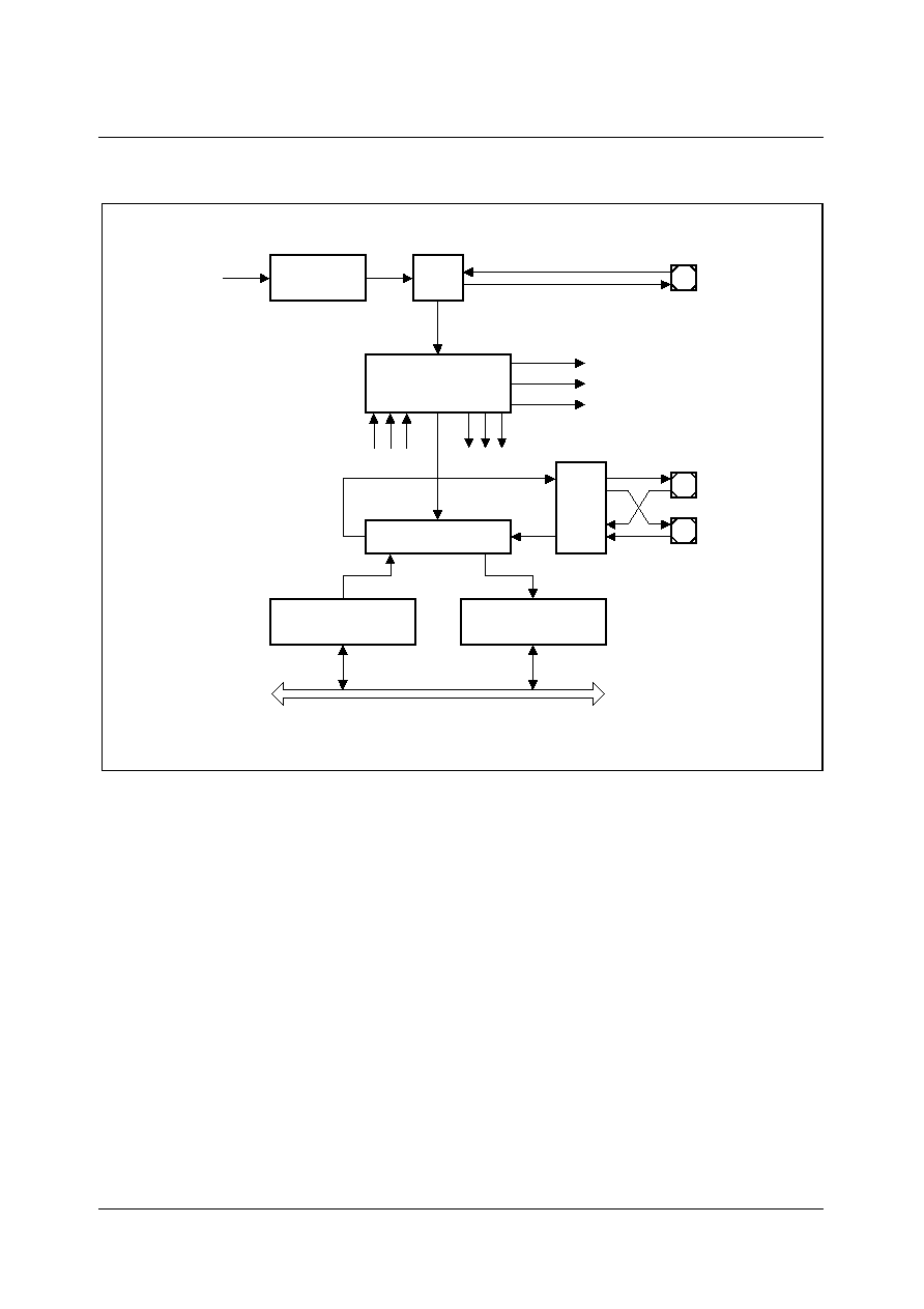
SDA 6000 / SDA 6001
PRELIMINARY DATA SHEET
Version 3.00
Peripherals
7 - 85
Micronas
Figure 7-39 Synchronous Serial Channel SSC0 Block Diagram
The operating mode of the serial channel SSC0 is controlled by its bit-addressable
control register SSCC0N. This register serves two purposes:
� during programming (SSC0 disabled by SSC0EN = `0') it provides access to a set of
control bits
� during operation (SSC enabled by SSC0EN = `1') it provides access to a set of status
flags
The shift register of the SSC0 is connected to both the transmit pin and the receive pin
via the pin control logic (see block diagram in Figure 7-39). Transmission and reception
of serial data is synchronized and takes place at the same time, e.g. the same number
of transmitted bits is also received. Transmit data is written into the Transmit Buffer
SSCTB. It is moved to the shift register as soon as this is empty. An SSC master
(SSC0MS = `1') immediately begins transmitting, while an SSC slave (SSC0MS = `0')
will wait for an active shift clock. When the transfer starts, the busy flag SSC0BSY is set
and a transmit interrupt request line (SSCTIR) will be activated to indicate that SSCTB
may be reloaded again. When the programmed number of bits (2 ... 16) has been
UEB11158
16-Bit Shift Register
MRSTx
Internal Bus
Receive Buffer
Register SSC0RB
Transmit Buffer
Register SSC0TB
MTSRx
Pin
Control
SSC Control Block
SSC0CON
Status
Control
SSC0EIR
SSC0TIR
SSC0RIR
Receive Int. Request
Transmit Int. Request
Error Int. Request
Control
Clock
Shift
Clock
Generator
Baud Rate
SCLKx
33 MHz

SDA 6000 / SDA 6001
PRELIMINARY DATA SHEET
Version 3.00
Peripherals
7 - 86
Micronas
transferred, the contents of the shift register are moved to the Receive Buffer SSCRB
and a receive interrupt request line (SSCRIR) will be activated. If no further transfer is to
take place (SSCTB is empty), SSC0BSY will be cleared at the same time. Software
should not modify SSC0BSY, as this flag is hardware controlled.
Note: Only one SSC (etc.) can be master at a given time.
The transfer of serial data bits can be programmed in many respects:
� The data width can be chosen from 2 bits to 16 bits
� A transfer may start with the LSB or the MSB
� The shift clock may be idle low or idle high
� The data bits may be shifted with the leading or trailing edge of the clock signal
� The baud rate may be set from 254 Baud up to 16.66 MBaud (@ 33.33 MHz module
clock)
� The shift clock can be generated (master) or received (slave)
These features allow the adaptation of the SSC0 to a wide range of applications, where
serial data transfer is required.
The Data Width Selection supports the transfer of frames of any data length, from 2-bit
`characters' up to 16-bit `characters'. Starting with the LSB (SSC0HB = `0') allows
communication e.g. with an SSC device in synchronous mode (C166 family) or 8051 like
serial interfaces. Starting with the MSB (SSC0HB = `1') allows operation compatible with
the SPI interface.
Regardless which data width is selected and whether the MSB or the LSB is transmitted
first, the transfer data is always right aligned in registers SSCTB and SSCRB, with the
LSB of the transfer data in bit 0 of these registers. The data bits are rearranged for
transfer by the internal shift register logic. The unselected bits of SSCTB are ignored, the
unselected bits of SSCRB will not be valid and should be ignored by the receiver service
routine.
The Clock Control allows the transmit and receive behavior of the SSC0 to be adapted
to a variety of serial interfaces. A specific clock edge (rising or falling) is used to shift out
transmit data, while the other clock edge is used to latch in receive data. Bit SSC0PH
selects the leading edge or the trailing edge for each function. Bit SSC0PO selects the
level of the clock line in the idle state. So for an idle-high clock the leading edge is a
falling one, a 1-to-0 transition (see Figure 7-40).
SDA 6000 / SDA 6001
PRELIMINARY DATA SHEET
Version 3.00
Peripherals
7 - 87
Micronas
Figure 7-40 Serial Clock Phase and Polarity Options
7.4.1
Full-Duplex Operation
The different devices are connected by three lines. The definition of these lines is always
determined by the master: the line connected to the master's data output pin MTSR is
the transmit line, the receive line is connected to its data input line MRST, and the clock
line is connected to pin SCLK. Only the device selected for master operation generates
and outputs the serial clock on pin SCLK. All slaves receive this clock, so their pin SCLK
must be switched to input mode. The output of the master's shift register is connected to
the external transmit line, which in turn is connected to the slaves' shift register input.
The output of the slaves' shift register is connected to the external receive line in order
to enable the master to receive the data shifted out of the slave. The external
connections are hard-wired, the function and direction of these pins is determined by the
master or slave operation of the individual device.
Note: The shift direction shown in the diagram applies to MSB-first operation as well as
to LSB-first operation.
When initializing the devices in this configuration, one device must be selected for
master operation while all other devices must be programmed for slave operation.
Initialization includes the operating mode of the device's SSC and also the function of
the respective port lines.
UED11159
SSC0
PO
SSC0
PH
0
0
0
1
1
0
1
1
Pins
MTSR0/MRST0
Transmit Data
Shift Clock
SCLK
Shift Data
First Bit
Latch Data
Last Bit
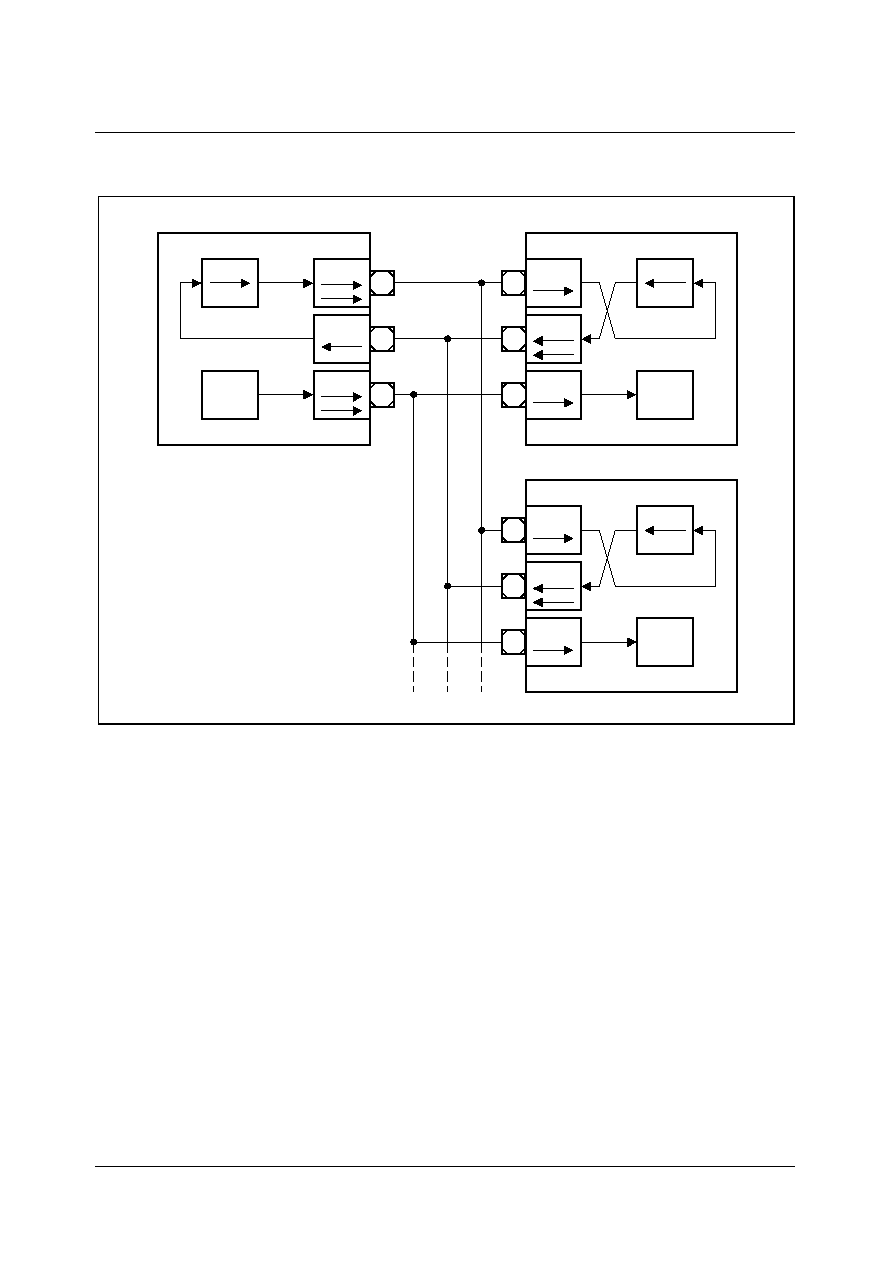
SDA 6000 / SDA 6001
PRELIMINARY DATA SHEET
Version 3.00
Peripherals
7 - 88
Micronas
Figure 7-41 SSC0 Full Duplex Configuration
The data output pins MRST of all slave devices are connected together onto the one
receive line in this configuration. During a transfer; each slave shifts out data from its shift
register. There are two ways to avoid collisions on the receive line due to different slave
data:
� Only one slave drives the line, e.g. enables the driver of its MRST pin. All the other
slaves have to program their MRST pins to input. So only one slave can put its data
onto the master's receive line. Only receiving of data from the master is possible. The
master selects the slave device from which it expects data either by separate select
lines, or by sending a special command to this slave. The selected slave then switches
its MRST line to output, until it gets a deselection signal or command.
� The slaves use open drain output on MRST. This forms a wired-AND connection.
The receive line needs an external pullup in this case. Corruption of the data on the
receive line sent by the selected slave is avoided, when all slaves which are not
selected for transmission to the master only send ones (`1'). Since this high level is not
actively driven onto the line, but only held through the pullup device, the selected slave
can actively pull this line to a low level when transmitting a zero bit. The master selects
Transmit
MTSR
MRST
CLK
Clock
Shift Register
Device #1
Master
MTSR
MRST
CLK
Receive
Clock
Shift Register
Clock
Device #2
Slave
CLK
MRST
Device #3
MTSR
Clock
Shift Register
Slave
UED11160

SDA 6000 / SDA 6001
PRELIMINARY DATA SHEET
Version 3.00
Peripherals
7 - 89
Micronas
the slave device from which it expects data either by separate select lines, or by
sending a special command to this slave.
After performing all necessary initializations of the SSC0, the serial interfaces can be
enabled. In a master device, the alternate clock line will now go to its programmed
polarity. The alternate data line will go to either `0' or `1', until the first transfer starts. After
a transfer, the alternate data line will always remain at the logic level of the last
transmitted data bit.
When the serial interfaces are enabled, the master device can initiate the first data
transfer by writing the transmit data into register SSCTB. This value is copied into the
shift register (which is assumed to be empty at this time), and the selected first bit of the
transmit data will be placed onto the MTSR line on the next clock to the baud rate
generator (transmission only starts, if SSC0EN = `1'). Depending on the selected clock
phase, a clock pulse will also be generated on the SCLK line. With the opposite clock
edge the master simultaneously latches and shifts in the data detected at its input line
MRST. This `exchanges' the transmit data with the receive data. Since the clock line is
connected to all slaves, their shift registers will be shifted synchronously with the
master's shift register, shifting out the data contained in the registers, and shifting in the
data detected at the input line. After the pre-programmed number of clock pulses (via the
data width selection) the data transmitted by the master is contained in all slaves' shift
registers, while the master's shift register holds the data of the selected slave. In the
master and all the slaves, the content of the shift register is copied into the receive buffer
SSCRB and the receive interrupt line SSC0RIR is activated.
A slave device will immediately output the selected first bit (MSB or LSB of the transfer
data) at pin MRST, when the content of the transmit buffer is copied into the slave's shift
register. It will not wait for the next clock from the baud rate generator, as the master
does. The reason for this is that, depending on the selected clock phase, the first clock
edge generated by the master may be already used to clock in the first data bit. So the
slave's first data bit must already be valid at this time.
Note: On the SSC0 a transmission and a reception always takes place at the same time,
regardless whether valid data has been transmitted or received.
The initialization of the SCLK pin on the master requires some attention in order to
avoid undesired clock transitions, which may disturb the other receivers. The state of the
internal alternate output lines is `1' as long as the SSC is disabled. This alternate output
signal is ANDed with the respective port line output latch. Enabling the SSC with an idle-
low clock (SSC0PO = `0') will immediately drive the alternate data output and (via the
AND) the port pin SCLK low. To avoid this, the following sequence should be used:
� select the clock idle level (SSC0PO = `x')
� load the port output latch with the desired clock idle level
� switch the pin to output
� enable the SSC0 (SSC0EN = `1')
� if SSC0PO = `0': enable alternate data output

SDA 6000 / SDA 6001
PRELIMINARY DATA SHEET
Version 3.00
Peripherals
7 - 90
Micronas
The same mechanism as for selecting a slave for transmission (separate select lines or
special commands) may also be used to move the role of the master to another device
in the network. In this case the previous master and the future master (previous slave)
will have to toggle their operating mode (SSC0MS) and the direction of their port pins.
7.4.2
Half Duplex Operation
In a half duplex configuration only one data line is necessary for both receiving and
transmitting of data. The data exchange line is connected to both the MTSR and MRST
pins in each device, the clock line is connected to the SCLK pin.
The master device controls the data transfer by generating the shift clock, while the slave
devices receive it. Due to the fact that all transmit and receive pins are connected to the
one data exchange line, serial data may be moved between arbitrary stations.
Similar to full duplex mode there are two ways to avoid collisions on the data
exchange line:
� only the transmitting device may enable its transmit pin driver
� the non-transmitting devices use open drain output and only send ones.
Since the data inputs and outputs are connected together, a transmitting device will clock
in its own data at the input pin (MRST for a master device, MTSR for a slave). By these
means any corruptions on the common data exchange line, where the received data is
not equal to the transmitted data are detected.
SDA 6000 / SDA 6001
PRELIMINARY DATA SHEET
Version 3.00
Peripherals
7 - 91
Micronas
Figure 7-42 SSC Half Duplex Configuration
7.4.3
Continuous Transfers
When the transmit interrupt request flag is set, it indicates that the transmit buffer SSCTB
is empty and ready to be loaded with the next transmit data. If SSCTB has been reloaded
by the time the current transmission is finished, the data is immediately transferred to the
shift register and the next transmission starts without any additional delay. On the data
line there is no gap between the two successive frames. For example, two byte transfers
would look the same as one word transfer. This feature can be used to interface with
devices which can operate with or require more than 16 data bits per transfer. How long
a total data frame length can be depends on the software. This option can also be used
e.g. to interface to byte-wide and word-wide devices on the same serial bus.
Note: Of course, this can only happen in multiples of the selected basic data width, since
it would require disabling/enabling of the SSC0 to reprogram the basic data width
on-the-fly.
Transmit
MTSR
MRST
CLK
Clock
Shift Register
Device #1
Master
MTSR
MRST
CLK
Clock
Shift Register
Clock
Device #2
Slave
CLK
MRST
Device #3
MTSR
Clock
Shift Register
Slave
UED11161
Common
Transmit/
Receive
Line

SDA 6000 / SDA 6001
PRELIMINARY DATA SHEET
Version 3.00
Peripherals
7 - 92
Micronas
7.4.4
Port Control
The SSC0 uses three pins to communicate with the external world. Pin SCLK serves as
the clock line, while pins MRST (Master Receive/Slave Transmit) and MTSR (Master
Transmit/Slave Receive) serve as the serial data input/output lines.
The operation of the SSC0 pins depends on the selected operating mode (master or
slave). The direction of the port lines depends on the operating mode. The SSC0 will
automatically use the correct alternate input or output line of the ports when switching
modes. The direction of the port pins, however, must be programmed by the user. Using
the open drain output feature of the port lines helps to avoid bus contention problems
and reduces the need for hardwired hand-shaking or slave select lines. In this case it is
not always necessary to switch the direction of a port pin.
7.4.5
Baud Rate Generation
The serial channel SSC0 has its own dedicated 16-bit baud rate generator with 16-bit
reload capability, allowing baud rate generation independent from the timers. In addition
to Figure 7-39, Figure 7-43 shows the baud rate generator of the SSC0 in more detail.
Figure 7-43 SSC0 Baud Rate Generator
The baud rate generator is clocked with the module clock 33.33 MHz. The timer is
counting downwards. Register SSCBR is the dual-function Baud Rate Generator/Reload
register. Reading SSCBR, while the SSC0 is enabled, returns the content of the timer.
Reading SSCBR, while the SSC0 is disabled, returns the programmed reload value. In
this mode the desired reload value can be written to SSCBR.
Note: Never write to SSCBR, while the SSC0 is enabled.
UES11162
16-Bit Reload Register
16-Bit Counter
f
SCLK
2
�
33 MHz
SCLKmax
f
in master mode
_
< 33 MHz / 2
in slave mode
SCLKmax
f
33 MHz / 4
<
_

SDA 6000 / SDA 6001
PRELIMINARY DATA SHEET
Version 3.00
Peripherals
7 - 93
Micronas
The formulas below calculate either the resulting baud rate for a given reload value, or
the required reload value for a given baud rate:
<SSCBR> represents the content of the reload register, taken as an unsigned 16-bit
integer while Baud rate
SSC
is equal to
f
SCLK
as shown in Figure 7-43.
The maximum baud rate that can be achieved when using a module clock of 33.33 MHz
is 16.6 MBaud in master mode (with <SSCBR> = 0000
H
) and 8.33 MBaud in slave mode
(with <SSCBR> = 0001
H
) lists some possible baud rates together with the required
reload values and the resulting bit times, assuming a module clock of 33.33 MHz.
7.4.6
Error Detection Mechanisms
The SSC0 is able to detect four different error conditions. Receive Error and Phase Error
are detected in all modes, while Transmit Error and baud rate Error only apply to slave
mode. When an error is detected, the respective error flag is set and an error interrupt
request will be generated by activating the SSCEIR line (see Figure 7-44). The error
interrupt handler may then check the error flags to determine the cause of the error
interrupt. The error flags are not reset automatically but rather must be cleared by
software after servicing. This allows some error conditions to be serviced via interrupt,
while the others may be polled by software.
Note: The error interrupt handler must clear the associated (enabled) error-flag(s) to
prevent repeated interrupt requests.
) - 1
Baud rate
SSC0
=
2
�
(<SSCBR> + 1)
33 MHz
<SSCBR> = (
2
�
Baud rate
SSC0
33 MHz
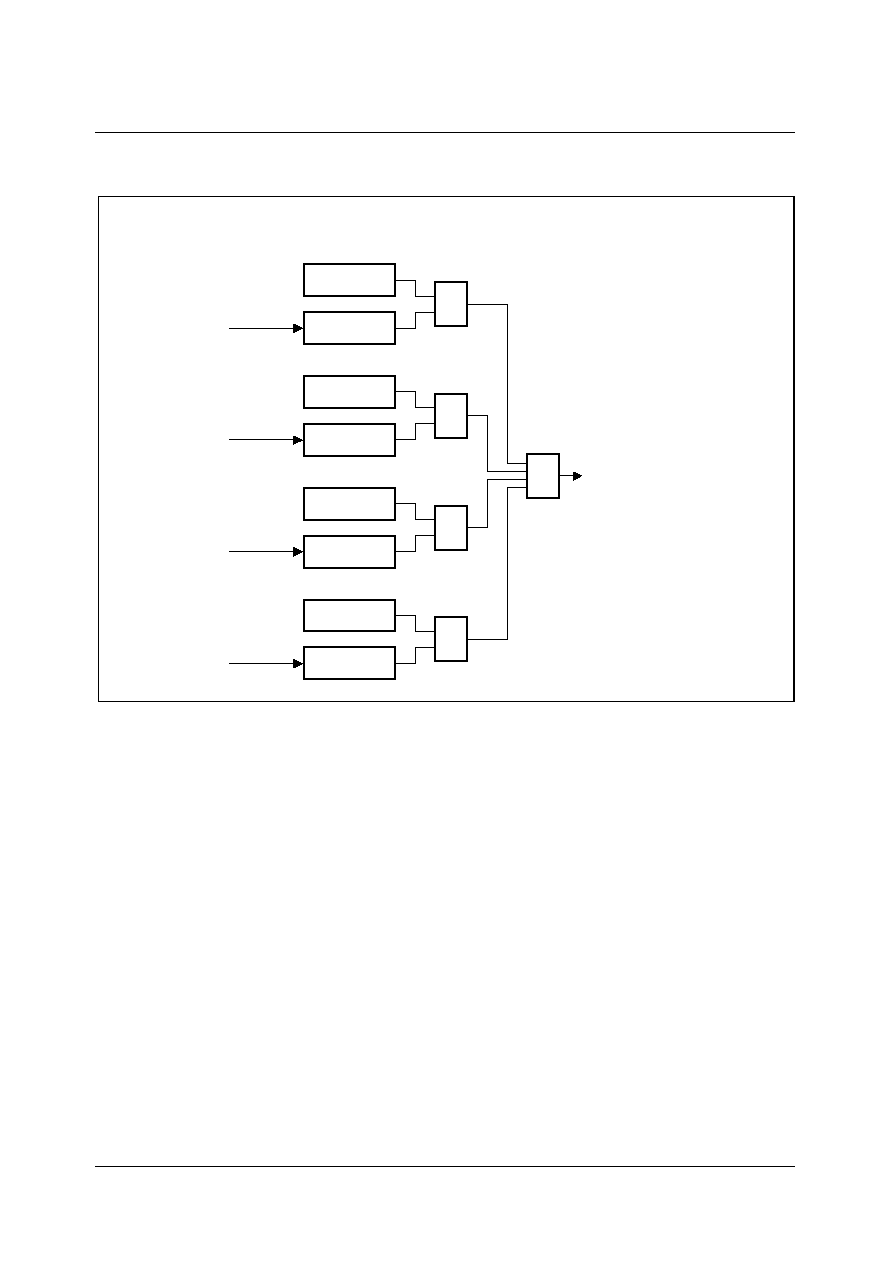
SDA 6000 / SDA 6001
PRELIMINARY DATA SHEET
Version 3.00
Peripherals
7 - 94
Micronas
Figure 7-44 SSC0 Error Interrupt Control
A Receive Error (Master or Slave mode) is detected, when a new data frame is
completely received, but the previous data was not read out of the receive buffer register
SSCRB. This condition sets the error flag SSC0RE and, when enabled via SSC0REN,
the error interrupt request line SSCEIR. The old data in the receive buffer SSCRB will be
overwritten with the new value and is unretrievably lost.
A Phase Error (Master or Slave mode) is detected, when the incoming data at pin
MRST0 (master mode) or MTSR0 (slave mode), sampled with the same frequency as
the module clock, changes between one cycle before and two cycles after the latching
edge of the shift clock signal SCLK. This condition sets the error flag SSC0PE and, when
enabled via SSC0PEN, the error interrupt request flag SSCEIR.
A Baud Rate Error (Slave mode) is detected, when the incoming clock signal deviates
from the programmed baud rate by more than 100%, e.g. it is either more than double
or less than half the expected baud rate. This condition sets the error flag SSC0BE and,
when enabled via SSC0BEN, the error interrupt request line SSCEIR. Using this error
detection capability requires that the slave's baud rate generator is programmed to the
same baud rate as the master device. This feature detects false additional, or missing
pulses on the clock line (within a certain frame).
UES11163
SSC0TEN
&
SSC0TE
Transmit
Error
SSC0REN
SSC0RE
Error
Receive
&
SSC0PE
SSC0PEN
Phase
Error
&
SSC0BE
SSC0BEN
Baud Rate
Error
&
1
Error Interrupt
SSCEIR
Bit in Register
SSCCON
_
<

SDA 6000 / SDA 6001
PRELIMINARY DATA SHEET
Version 3.00
Peripherals
7 - 95
Micronas
Note: If this error condition occurs and bit SSC0REN = `1', an automatic reset of the
SSC0 will be performed in case of this error. This is done to re-initialize the SSC0,
if too few or too many clock pulses have been detected.
A Transmit Error (Slave mode) is detected, when a transfer is initiated by the master
(shift clock gets active), but the transmit buffer SSCTB of the slave was not updated
since the last transfer. This condition sets the error flag SSC0TE and, when enabled via
SSC0TEN, the error interrupt request line SSC0EIR. If a transfer starts while the transmit
buffer is not updated, the slave will shift out the `old' contents of the shift register, which
is normally the data received during the last transfer. This may lead to the corruption of
the data on the transmit/receive line in half-duplex mode (open drain configuration), if
this slave is not selected for transmission. This mode requires that slaves not selected
for transmission only shift out ones, e.g. their transmit buffers must be loaded with
`FFFF
H
' prior to any transfer.
Note: A slave with push/pull output drivers, which is not selected for transmission, will
normally have its output drivers switched. However, in order to avoid possible
conflicts or misinterpretations, it is recommended to always load the slave's
transmit buffer prior to any transfer.
The cause of an error interrupt request (receive, phase, baud rate, transmit error) can be
identified by the error status flags in control register SSCCON.
Note: In contrary to the error interrupt request line SSCEIR, the error status flags
SSC0TE, SSC0RE, SSC0PE, and SSC0BE, which are located in register
SSCCON, are not reset automatically upon entry into the error interrupt service
routine, but must be cleared by software.

SDA 6000 / SDA 6001
PRELIMINARY DATA SHEET
Version 3.00
Peripherals
7 - 96
Micronas
7.4.7
Register Description
The operating mode of the serial channel SSC0 is controlled by its control register
SSCCON. This register contains control bits for mode and error check selection, and
status flags for error identification. Depending on bit SSC0EN, either control functions or
status flags and master/slave control is enabled.
SSC0EN = 0: Programming Mode
SSCCON
Reset Value: 0000
H
Bit
Function
SSC0BM
SSC0 Data Width Selection
0:
Reserved. Do not use this combination.
1 ... 15: Transfer Data Width is 2 ... 16 bit (<SSC0BM>+1)
SSC0HB
SSC0 Heading Control Bit
0:
Transmit/Receive LSB First
1:
Transmit/Receive MSB First
SSC0PH
SSC0 Clock Phase Control Bit
0:
Shift transmit data on the leading clock edge, latch on trailing edge
1:
Latch receive data on leading clock edge, shift on trailing edge
SSC0PO
SSC0 Clock Polarity Control Bit
0:
Idle clock line is low, leading clock edge is low-to-high transition
1:
Idle clock line is high, leading clock edge is high-to-low transition
SSC0LB
SSC0 Loop Back Bit
0:
Normal output
1:
Receive input is connected with transmit output (half duplex mode)
SSC0TEN
SSC0 Transmit Error Enable Bit
0:
Ignore transmit errors
1:
Check transmit errors
SSC0REN
SSC0 Receive Error Enable Bit
0:
Ignore receive errors
1:
Check receive errors
5
4
3
2
1
0
11
10
9
8
7
6
15
14
13
12
rw
rw
rw
rw
rw
rw
rw
rw
rw
rw
rw
rw
SSC0
EN
SSC0
MS
-
SSC0
AREN
SSC0
BEN
SSC0
PEN
SSC0
REN
SSC0
TEN
SSC0
LB
SSC0
PO
SSC0
PH
SSC0
HB
SSC0BM

SDA 6000 / SDA 6001
PRELIMINARY DATA SHEET
Version 3.00
Peripherals
7 - 97
Micronas
SSC0PEN
SSC0 Phase Error Enable Bit
0:
Ignore phase errors
1:
Check phase errors
SSC0BEN
SSC0 Baud Rate Error Enable Bit
0:
Ignore baud rate errors
1:
Check baud rate errors
SSC0AREN SSC0 Automatic Reset Enable Bit
0:
No additional action upon a baud rate error
1:
The SSC is automatically reset upon a baud rate error
SSC0MS
SSC0 Master Select Bit
0:
Slave Mode. Operate on shift clock received via SCLK.
1:
Master Mode. Generate shift clock and output it via SCLK.
SSC0EN
SSC0 Enable Bit = `0'
Transmission and reception disabled. Access to control bits.
Bit
Function
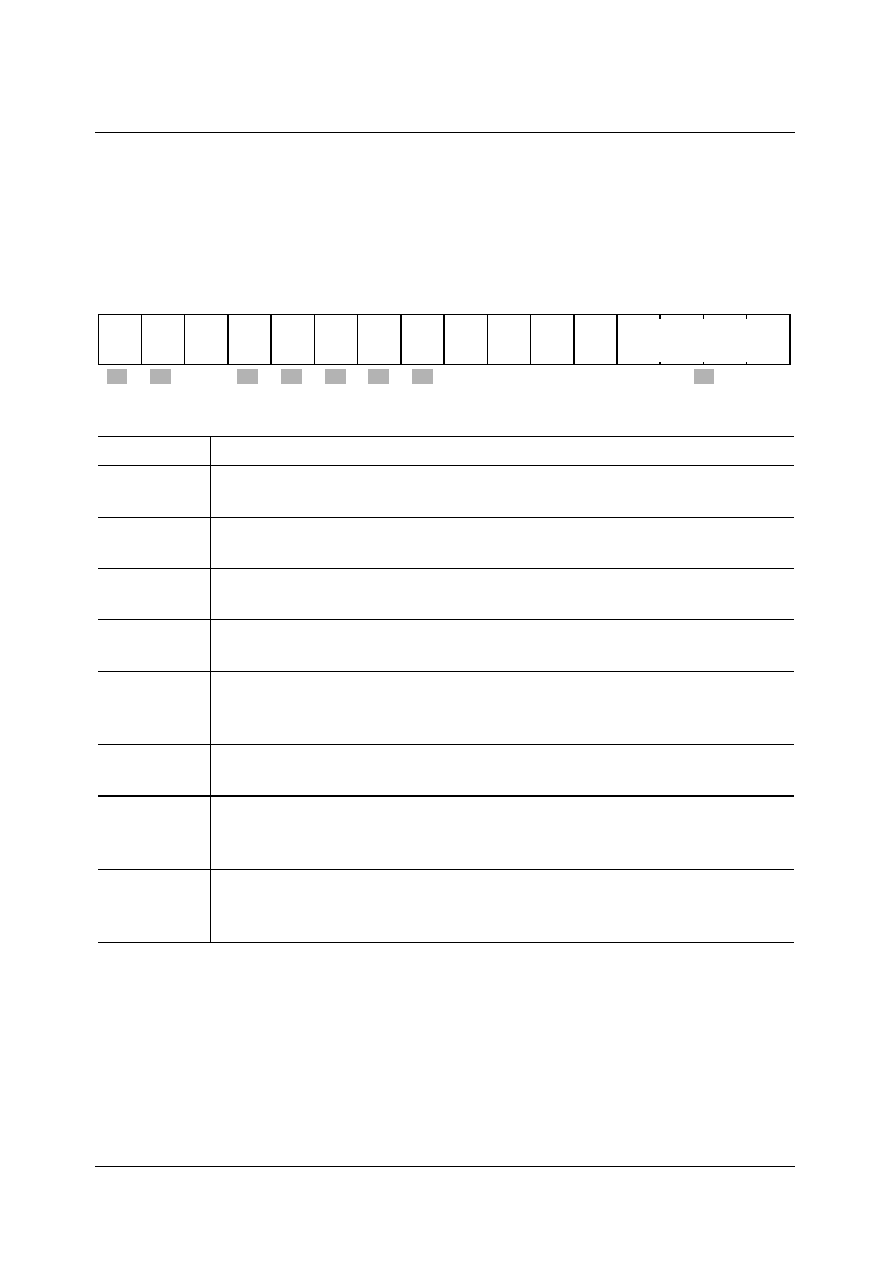
SDA 6000 / SDA 6001
PRELIMINARY DATA SHEET
Version 3.00
Peripherals
7 - 98
Micronas
SSC0EN = 1: Operating Mode
SSCCON
Reset Value: 0000
H
Note: The target of an access to SSCCON (control bits or flags) is determined by the
state of SSC0EN prior to the access, i.e. writing C057
H
to SSC0CON in
programming mode (SSC0EN = `0') will initialize the SSC (SSC0EN was `0') and
then switch it on (SSC0EN = `1').
When writing to SSCCON, make sure that zeros are input to reserved locations.
The SSC0 baud rate timer reload register SSCBR contains the 16-bit reload value for the
baud rate timer.
Bit
Function
SSC0BC
SSC0 Bit Count Field
Shift counter is updated with every shifted bit. Do not write to!!!
SSC0TE
SSC0 Transmit Error Flag
1:
Transfer starts with the slave's transmit buffer not being updated
SSC0RE
SSC0 Receive Error Flag
1:
Reception completed before the receive buffer was read
SSC0PE
SSC0 Phase Error Flag
1:
Received data changes around sampling clock edge
SSC0BE
SSC0 Baud Rate Error Flag
1:
More than factor 2 or 0.5 between Slave's actual and
expected baud rate
SSC0BSY
SSC0 Busy Flag
Set while a transfer is in progress. Do not write to!!!
SSC0MS
SSC0 Master Select Bit
0:
Slave Mode. Operate on shift clock received via SCLK.
1:
Master Mode. Generate shift clock and output it via SCLK.
SSC0EN
SSC0 Enable Bit = `1'
Transmission and reception enabled. Access to status flags and M/S
control.
5
4
3
2
1
0
11
10
9
8
7
6
15
14
13
12
rw
rw
r
rw
rw
rw
rw
rw
SSC0
EN
SSC0
MS
-
SSC0
BSY
SSC0
BE
SSC0
PE
SSC0
RE
SSC0
TE
-
-
-
-
SSC0BC

SDA 6000 / SDA 6001
PRELIMINARY DATA SHEET
Version 3.00
Peripherals
7 - 99
Micronas
SSCBR
Reset Value: 0000
H
The SSC0 transmitter buffer register SSCTB contains the transmit data value.
SSCTB
Reset Value: 0000
H
The SSC0 receiver buffer register SSCRB contains the receive data value.
Bit
Function
SSC0RL
(15 ... 0)
Baud Rate Timer/Reload Register Value
Reading SSCBR returns the 16-bit content of the baud rate timer. Writing
SSC0BR loads the baud rate timer reload register.
Bit
Function
SSC0TD
(15 ... 0)
Transmit Data Register Value
SSCTB contains the data to be transmitted. Unselected bits of SSC0TB
are ignored during transmission.
5
4
3
2
1
0
11
10
9
8
7
6
15
14
13
12
rw
SSC0RL(15 ..0)
5
4
3
2
1
0
11
10
9
8
7
6
15
14
13
12
rw
SSC0TD(15..0)

SDA 6000 / SDA 6001
PRELIMINARY DATA SHEET
Version 3.00
Peripherals
7 - 100
Micronas
SSCRB
Reset Value: 0000
H
Bit
Function
SSC0RD
(7 ... 0)
Receive Data Register Value
SSCRB contains the received data bits. Unselected bits of SSC0RB will
be not valid and should be ignored
5
4
3
2
1
0
11
10
9
8
7
6
15
14
13
12
r
SSC0RD(15..0)

SDA 6000 / SDA 6001
PRELIMINARY DATA SHEET
Version 3.00
Peripherals
7 - 101
Micronas
7.5
I
2
C-Bus Interface
The on-chip I
2
C Bus module connects the M2 to other external controllers and/or
peripherals via the two-line serial I
2
C interface. The I
2
C Bus module provides
communication at data rates of up to 400 Kbit/s and features 7-bit as well as 10-bit
addressing.
The module can operate in three different modes:
Master mode, where the I
2
C controls the bus transactions and provides the clock signal.
Slave mode, where an external master controls the bus transactions and provides the
clock signal.
Multimaster mode, where several masters can be connected to the bus, i.e. the I
2
C can
be master or slave.
The on-chip I
2
C bus module allows efficient communication via the common I
2
C bus. The
module unloads the CPU of low level tasks such as
� (De)Serialization of bus data.
� Generation of start and stop conditions.
� Monitoring the bus lines in slave mode.
� Evaluation of the device address in slave mode.
� Bus access arbitration in multimaster mode.
Features
� Extended buffer allows up to 4 send/receive data bytes to be stored.
� Support of standard 100 KBaud and extended 400 KBaud data rates.
� Operation in 7-bit or 10-bit addressing mode.
� Flexible control via interrupt service routines or by polling.
7.5.1
Operational Overview
Data is transferred by the 2-line I
2
C bus (SDA, SCL) using a protocol that ensures
reliable and efficient transfers. This protocol clearly distinguishes regular data transfers
from defined control signals which control the data transfers.
The following bus conditions are defined:
Bus Idle:
SDA and SCL remain high. The I
2
C bus is currently not used.
Data Valid:
SDA stable during the high phase of SCL. SDA then represents the
transferred bit. There is one clock pulse for each transferred bit of data.
During data transfers SDA may only change while SCL is low (see
below)!
Start Transfer: A falling edge on SDA ( ) while SCL is high indicates a start condition.
This start condition initiates a data transfer over the I
2
C bus.

SDA 6000 / SDA 6001
PRELIMINARY DATA SHEET
Version 3.00
Peripherals
7 - 102
Micronas
Stop Transfer: A rising edge on SDA ( ) while SCL is high indicates a stop condition.
This stop condition terminates a data transfer. An arbitrary number of
bytes may be transferred between a start condition and a stop condition.
7.5.2
The Physical I
2
C-Bus Interface
Communication via the I
2
C Bus uses two bidirectional lines, the serial data line SDA and
the serial clock line SCL. Each of these two generic interface lines can be connected to
a number of IO port lines. These connections can be established and released under
software control.
Figure 7-45 I
2
C Bus Line Connections
UES11164
SDAx
SDA0
SCL0
SCLx
C Module
2
Generic Data Line
Generic Clock Line

SDA 6000 / SDA 6001
PRELIMINARY DATA SHEET
Version 3.00
Peripherals
7 - 103
Micronas
This mechanism allows a number of configurations of the physical I
2
C Bus interface:
Physical Channels
Can be selected, so the I
2
C module can use electrically separated channels or increase
the addressing range by using more data lines.
Note: Baud rate and physical channels should never be changed (via ICCFG) during a
transfer.
Channel Switching
The I
2
C module can be connected to a specific pair of pins (e.g. SDA0 and SCL0) which
then forms a separate I
2
C channel to the external system. The channel can be
dynamically switched by connecting the module to another pair of pins (e.g. SDA1 and
SCL1). This establishes physically separate interface channels.
Broadcasting:
Connecting the module to more than one pair of pins (e.g. SDA0/1 and SCL0/1) allows
the transmission of messages over multiple physical channels at the same time. Please
note that this configuration is critical when the M2 is a slave. In master mode it cannot
be guaranteed that all selected slaves have reached the message.
Register ICCFG selects the bus baud rate as well the activation of SDA and SCL lines.
So an external I
2
C channel can be established (baud rate and physical lines) with one
single register access.
Note: Respective port pin definition
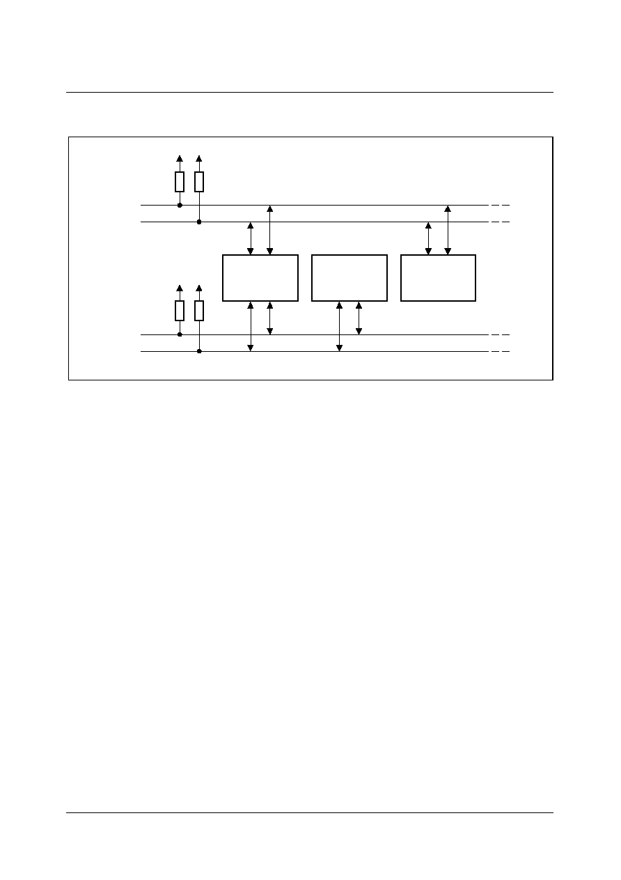
SDA 6000 / SDA 6001
PRELIMINARY DATA SHEET
Version 3.00
Peripherals
7 - 104
Micronas
Figure 7-46 Physical Bus Configuration Example
Output Pin Configuration
The pin drivers that are assigned to the I
2
C channel(s) provide open drain outputs (i.e.
no upper transistor). This ensures that the I
2
C module does not put any load on the I
2
C
bus lines while the M2 is not powered. The I
2
C bus lines therefore require external pull-
up resistors (approx. 10 K
for operation at 100 KBaud, 2 K
for operation at
400 KBaud).
All pins of the M2 that are to be used for I
2
C bus communication must be switched to
output, opendrain and their alternate function must be enabled (by setting the respective
port output latch to `1'), before any communication can be established.
If not driven by the I
2
C module (i.e. the corresponding enable bit in register ICCFG is `0')
they then switch off their drivers (i.e. driving `1' to an open drain output). Due to the
external pull-up devices the respective bus levels will then be `1' which is idle.
The I
2
C module features digital input filters in order to improve the noise output from the
external bus lines.
UES11165
SDA 6000
SCL
SDA
C-Bus Node
2
C-Bus Node
2
C-Channel 0
2
SDA
SCL
C-Channel 1
2

SDA 6000 / SDA 6001
PRELIMINARY DATA SHEET
Version 3.00
Peripherals
7 - 105
Micronas
7.5.3
Functional Overview
Operation in Master Mode
If the on-chip I
2
C module controls the I
2
C bus (i.e. bus master), master mode must be
selected via bit field MOD in register ICCON. The physical channel is configured by a
control word written to register ICCFG, defining the active interface pins and the used
baud rate. More than one SDA and/or SCL line may be active at a time. The address of
the remote slave that is to be accessed is written to ICRTB0 ... 3. The bus is claimed by
setting bit BUM in register ICCON. This generates a start condition on the bus and
automatically starts the transmission of the address in ICRTB0. Bit TRX in register
ICCON defines the transfer direction (TRX = `1', i.e. transmit, for the slave address). A
repeated start condition is generated by setting bit RSC in register ICCON, which
automatically starts the transmission of the address previously written to ICRTB0. This
may be used to change the transfer direction. RSC is cleared automatically after the
repeated start condition has been generated.
The bus is released by clearing bit BUM in register ICCON. This generates a stop
condition on the bus.
Note: Between load the address in ICRTB0 an setting bit BUM at least one command
(nop) has to be executed.
Operation in Multimaster Mode
If multimaster mode is selected via bit field MOD in register ICCON, the on-chip I
2
C
module can operate concurrently as a bus master or as a slave. The descriptions of
these modes apply accordingly.
Multimaster mode implies that several masters are connected to the same bus. As more
than one master may try to claim the bus at a given time, an arbitration is done on the
SDA line. When a master device detects a mismatch between the data bit to be sent and
the actual level on the SDA (bus) line, it looses the arbitration and automatically switches
to slave mode (leaving the other device as the remaining master). This loss of arbitration
is indicated by bit AL in register ICST which must be checked by the driver software when
operating in multimaster mode. Lost arbitration is also indicated when the software tries
to claim the bus (by setting bit BUM) while the I
2
C bus is active (indicated by bit BB = `1').
Bit AL must be cleared via software.
Operation in Slave Mode
If the on-chip I
2
C module is controlled via the I
2
C bus by a remote master (i.e. be a bus
slave), slave mode must be selected via bit field MOD in register ICCON. The physical
channel is configured by a control word written to register ICCFG, defining the active
interface pins and the used baud rate. It is recommended to have only one SDA and SCL

SDA 6000 / SDA 6001
PRELIMINARY DATA SHEET
Version 3.00
Peripherals
7 - 106
Micronas
line active at a time when operating in slave mode. The address by which the slave
module can be selected is written to register ICADR.
The I
2
C module is selected by another master when it receives (after a start condition),
either its own device address (stored in ICADR) or the general call address (00
H
). In this
case an interrupt is generated and bit SLA in register ICST is set, indicating the valid
selection. The desired transfer mode is then selected via bit TRX (TRX = `0' for
reception, TRX = `1' for transmission).
For a transmission the respective data byte is placed into the buffer ICRTB0 ... 3
(which automatically sets bit TRX) and the acknowledge behavior is selected via bit
ACKDIS.
For a reception the respective data byte is fetched from the buffer ICRTB0 ... 3 after
IRQD has been activated.
In both cases the data transfer itself is enabled by clearing bits IRQD, IRQP and IRQE
which releases the SCL line.
When a stop condition is detected, bit SLA is cleared.
The I
2
C bus configuration register ICCFG selects the bus baud rate (partly) as well as
the activation of SDA and SCL lines. So an external I
2
C channel can be established
(baud rate and physical lines) with one single register access.
Systems that utilize several I
2
C channels can prepare a set of control words which
configure the respective channels. By writing one of these control words to ICCFG the
respective channel is selected. Different channels may use different baud rates. Also
different operating modes can be selected, e.g. enabling all physical interfaces for a
broadcast transmission.
Note: Refer also to Chapter 7.5.2.

SDA 6000 / SDA 6001
PRELIMINARY DATA SHEET
Version 3.00
Peripherals
7 - 107
Micronas
7.5.4
Registers
All available module registers are summarized in the overview table below.
I
2
C Configuration Register
ICCFG
Reset Value: 0000
H
Register
Name
Register Description
Address b/p
1)
1)
b: bit addressable / p: bit protected
Reset Value
ICCFG
I
2
C Configuration Register
00'E810
H
b
0000
H
ICCON
I
2
C Control Register
00'E812
H
b
0000
H
ICST
I
2
C Status Register
00'E814
H
b
0000
H
ICADR
I
2
C Address Register
00'E816
H
b
0000
H
ICRTBL
I
2
C Receive/Transmit Buffer
00'E818
H
�
0000
H
ICRTBH
I
2
C Receive/Transmit Buffer
00'E81A
H
�
0000
H
IICPISEL
2)
2)
Itus currently no function. Should be left on reset value.
I
2
C Port Input Select Register
00'E804
H
b
0000
H
15
14
13
12
11
10
9
8
7
6
5
4
3
2
1
0
BRPL
0
0
SCL
EN1
SCL
EN0
0
SDA
EN2
SDA
EN1
SDA
EN0
Field
Bits
Type
Value Description
SDAENx
(x = 2 ... 0)
2 ... 0
rw
0
1
Enable Input for Data Pin x
These bits determine to which pins the I
2
C data
line is connected.
SDA pin x is disconnected.
SDA pin x is connected with I
2
C data line.
SCLENx
(x = 3 ... 0)
5 ... 4
rw
0
1
Enable Input for Clock Pin x
These bits determine to which pins the I
2
C
clock line is connected.
SCL pin x is disconnected.
SCL pin x is connected with I
2
C clock line.
BRPL
15 ... 8
rw
�
Baud rate Prescaler Low
Determines the 8 least significant bits of the 10
bit baud rate prescaler. (See BPRH in ICADR.)
SDA 6000 / SDA 6001
PRELIMINARY DATA SHEET
Version 3.00
Peripherals
7 - 108
Micronas
I
2
C Control Register ICCON
Reset Value: 0000
H
15
14
13
12
11
10
9
8
7
6
5
4
3
2
1
0
WM
EN
0
0
0
CI
STP
IGE
TRX
INT
ACK
DIS
BU
M
MOD
RSC M10
Field
Bits
Type
Value
Description
M10
0
rw
0
1
Address Mode
7-bit addressing using ICA7 ... 1.
10-bit addressing using ICA9 ... 0.
RSC
1
rwh
0
1
Repeated Start Condition
No operation.
Generate a repeated start condition in
(multi) master mode. RSC cannot be set in
slave mode.
Note: RSC is cleared automatically after
the repeated start condition has been sent.
MOD
[3:2]
rwh
00
01
10
11
Basic Operating Mode
I
2
C module is disabled and initialized (Init-
Mode). Transmissions under execution will
be aborted.
Slave mode.
10
Master mode.
11
Multi-Master mode.
BUM
4
rwh
0
1
Busy Master
Clearing bit BUM ( ) generates a stop
condition immediately.
Setting bit BUM ( ) generates a start
condition in (multi)master mode.
Note: Setting bit BUM ( ) while BB = `1'
generates an arbitration lost situation.
In this case BUM is cleared and bit AL is
set.
BUM can not be set in slave mode.

SDA 6000 / SDA 6001
PRELIMINARY DATA SHEET
Version 3.00
Peripherals
7 - 109
Micronas
ACKDIS
5
rwh
0
1
Acknowledge Pulse Disable
An acknowledge pulse is generated for
each received frame.
No acknowledge pulse is generated.
Note: ACKDIS is automatically cleared by
a stop condition.
INT
6
rw
0
1
Interrupt Delete Select
Interrupt flag IRQD is deleted by read/write
to ICRTB0 ... 3.
Interrupt flag IRQD is not deleted by read/
write to ICRTB0 ... 3.
TRX
7
rwh
0
1
Transmit Select
No data is transmitted to the I
2
C bus.
Data is transmitted to the I
2
C bus.
Note: TRX is set automatically when
writing to the transmit buffer. It is not
allowed to delete this bit in the same
buscycle. It is automatically cleared after
last byte as slave transmitter.
IGE
8
rw
0
1
Ignore IRQE
Ignore IRQE (End of transmission)
interrupt.
The I
2
C is stopped at IRQE interrupt.
The I
2
C ignores the IRQE interrupt.
If RMEN is set, RM is mirrored here.
STP
9
rwh
0
1
Stop Master
0
Clearing bit STP generates no stop
condition.
1
Setting bit STP generates a stop
condition after next transmission.
BUM is set to zero.
ACKDIS is set to one.
STP is automatically cleared by a
stop condition.
If RMEN is set, RM is mirrored here.
Field
Bits
Type
Value
Description

SDA 6000 / SDA 6001
PRELIMINARY DATA SHEET
Version 3.00
Peripherals
7 - 110
Micronas
CI
[10:9] rw
00
01
10
11
Length of the Transmit Buffer
1 Byte
2 Bytes
3 Bytes
4 Bytes
If RMEN is set, RM is mirrored here.
WMEN
15
rwh
0
1
Write Mirror Enable
write mirror is not active
write mirror is active
If RMEN is set WMEN can not be set and
will remain zero. If WMEN and RMEN are
simultaneously set to 1, both will remain
what they are. So only one of each can be
set to 1.
RM
[15:8] rw �
Read
Mirror
If RMEN is set, RTB0 may be read here.
Writing to RM has no effect in this mode.
Field
Bits
Type
Value
Description

SDA 6000 / SDA 6001
PRELIMINARY DATA SHEET
Version 3.00
Peripherals
7 - 111
Micronas
I
2
C Status Register ICST
Reset Value: 0000
H
15
14
13
12
11
10
9
8
7
6
5
4
3
2
1
0
RM
EN
0
0
0
0
CO
IRQ
E
IRQ
P
IRQ
D
BB
LRB SLA
AL
ADR
Field
Bits
Type
Value Description
ADR
0
rh
�
Address
Bit ADR is set after a start condition in slave
mode until the address has been received
(1 byte in 7-bit address mode, 2 bytes in 10-
bit address mode).
AL
1
rwh
�
Arbitration Lost
Bit AL is set when the I
2
C module has tried
to become master on the bus, but has lost
the arbitration. Operation is continued until
the 9th clock pulse.
If multimaster mode is selected the I
2
C
module temporarily switches to slave mode
after a lost arbitration. Bit IRQP is set along
with bit AL.
AL must be cleared via software.
SLA
2
rh
0
1
Slave
The I
2
C module is not selected as a slave,
or the module is in master mode.
The I
2
C module has been selected as a
slave (device address received).
LRB
3
rh
�
Last Received Bit
Bit LRB represents the last bit (i.e. the
acknowledge bit) of the last transferred
frame.
It is automatically set to zero by a write or
read access to the buffer ICRTB0 ... 3.
Note: If LRB is high (no acknowledge) in
slave mode, TRX bit is set automatically.

SDA 6000 / SDA 6001
PRELIMINARY DATA SHEET
Version 3.00
Peripherals
7 - 112
Micronas
BB
4
rh
0
1
Bus Busy
The I
2
C bus is idle, i.e. a stop condition has
occurred.
The I
2
C bus is active, i.e. a start condition
has occurred.
Note: Bit BB is always `0' while the I
2
C
module is disabled.
IRQD
5
rwh
0
1
I
2
C Interrupt Request Bit for Data Transfer
Events
1)
No interrupt request pending.
A data transfer event interrupt request is
pending.
IRQD is set after the acknowledge bit of the
last byte has been received or transmitted,
and is cleared automatically upon a
complete read or write access to the
buffer(s) ICRTB0 ... 3.
New data transfers will start immediately
after clearing IRQD. Do not access any
register until next interrupt. If in polling
mode and CI is `0' only 8-Bit accesses to
the lower byte are allowed.
Note: If a multi byte write could not be
finished in slave mode because of missing
acknowledge, then the data interrupt is
followed by a end of transmission interrupt.
The number of bytes sent can be read from
CO. The data interrupt must have higher
priority than IRQE.
Field
Bits
Type
Value Description

SDA 6000 / SDA 6001
PRELIMINARY DATA SHEET
Version 3.00
Peripherals
7 - 113
Micronas
IRQP
6
rwh
0
1
I
2
C Interrupt Request Bit for Protocol
Events
1)
No interrupt request pending.
A protocol event interrupt request is
pending.
IRQP is set when bit SLA or bit AL is set
( ), and must be cleared via software.
If the I
2
C has been selected by an other
master, the software must look up the
required transmission direction by reading
the received address and direction bit,
stored in ICRTB0. The TRX-bit must
correspondingly be set by software.
IRQE
7
rwh
0
1
I
2
C Interrupt Request Bit for Data
Transmission End
1)
No interrupt request pending.
A receive end event interrupt request is
pending (a stop is detected).
IRQE is automatically cleared upon a start
condition. IRQE is not activated in init-
mode.
IRQE must always be deleted to continue
transmission.
Note: In slave mode IRQE is set after the
transmission is finished. This can also be
after a stop or RSC condition. In this case
the slave is not selected any more. This bit
is also set, if a transmission is stopped by a
missing acknowledge. In this case the bit
must be cleared by software.
Field
Bits
Type
Value Description

SDA 6000 / SDA 6001
PRELIMINARY DATA SHEET
Version 3.00
Peripherals
7 - 114
Micronas
1)
While IRQD, IRQP or IRQE is set and the I
2
C module is in master mode or has been selected as a slave, the
I
2
C clock line is held low which prevents further transfers on the I
2
C bus.
The clock line of the I
2
C bus is released when IRQD, IRQE and IRQP are cleared. Only in this case can the
next I
2
C bus action take place.
Interrupt request bits may be set or cleared via software, e.g. to control the I
2
C bus.
CO
10..8 rw
000
001
010
011
100
Counter of Transmitted Bytes Since Last
Data Interrupt. If a multi byte transmission
could not be finished because of a missing
acknowledge, the number of correctly
transferred bytes can be read from CO. It is
automatically set to zero by the correct
number (defined by CI) of write/read
accesses to the buffers ICRTB0 ... 3.
No Byte
1 Byte
2 Bytes
3 Bytes
4 Bytes
The number of legal bytes depends on the
data buffer size (CI). Writing to this bit field
does not affect its content.
If WMEN is set, WM is mirrored here.
WM
[15:8] wh
�
Write Mirror
If WMEN is set, RTB0 may be written here.
Reading WM will result in zero.
Field
Bits
Type
Value Description

SDA 6000 / SDA 6001
PRELIMINARY DATA SHEET
Version 3.00
Peripherals
7 - 115
Micronas
I
2
C Address Register ICADR
Reset Value: 0000
H
Baud Rate Selection
In order to give the user high flexibility in selection of CPU frequency and baud rate,
without constraints to baud rate accuracy, a flexible baud rate generator has been
15
14
13
12
11
10
9
8
7
6
5
4
3
2
1
0
BRP
MO
D
PREDIV
0
0
0
ICA
9/
0
ICA
8
IGE
ICA7..1
ICA
0/
0
Field
Bits
Type
Value Description
ICA0
0
rw
�
Node Address Bit 0 in 10-Bit Mode
(See ICCON bit M10)
Access is only possible in 10-bit mode.
�
0
0
0
Reserved read/write 0 if in 7-bit mode.
ICA7 ... 1
7..1
rw
�
Node Address in 7-Bit Mode (ICA9 and
ICA0 disregarded, ICA8 becomes IGE-bit).
IGE
8
rw
0
1
Ignore IRQE
In 7-bit mode, this bit becomes IGE-bit:
Ignore IRQE (End of transmission)
interrupt.
The I
2
C is stopped at IRQE interrupt.
The I
2
C ignores the IRQE interrupt.
Access is only possible in 7-bit mode.
ICA8
8
rw
�
Node Address Bit 8 in 10-Bit Mode
Access is only possible in 10-bit mode.
ICA9..0
9..0
rw
�
Node Address in 10-Bit Mode (all bits
used).
Note: Access is only possible in 10-bit
mode.
PREDIV
[14:13]
rw
00
01
10
11
Pre Divider for Baud Rate Generation
pre divider is disabled
pre divider factor 8 is enabled
pre divider factor 64 is enabled
reserved, do not use
BRPMOD
15
rw
0
1
Baud Rate Prescaler Mode
Mode 0 is enabled (by default)
Mode 1 is enabled.
SDA 6000 / SDA 6001
PRELIMINARY DATA SHEET
Version 3.00
Peripherals
7 - 116
Micronas
implemented. It uses two different modes and an additional pre divider. Low baud rates
may be configured at high precision in mode 0 which is compatible with older versions.
High baud rates may be configured precisely in mode 1.
Mode 0: Reciprocal Divider
The resulting baud rate is
Mode 1: Fractional Divider
The resulting baud rate is
Table 7-24
I
2
C-Bus Baud Rate Selection @ 33.33 MHz CPU-Freq.
BRPMOD
BRP @ 100 kBaud
BRP @ 400 kBaud
PREDIV
= 00
B
PREDIV
= 01
B
PREDIV
= 10
B
PREDIV
= 00
B
PREDIV
= 01
B
PREDIV
= 10
B
0
52
H
0A
H
1
H
14
H
02
H
�
1
03
H
�
�
0C
H
02
H
�
B
IIC
f
cpu
4
BRP 1
+
(
)
-----------------------------------
=
BRP
f
cpu
4 B
IIC
------------------ 1
�
=
B
IIC
f
cpu
BRP
1024
---------------------------
=
BRP
1024 B
IIC
f
cpu
----------------------------
=

SDA 6000 / SDA 6001
PRELIMINARY DATA SHEET
Version 3.00
Peripherals
7 - 117
Micronas
I
2
C Receive/Transmit Buffer ICRTBH/L
Reset Value: 0000
H
1)
A read respectively a write access (depending on bit TRX) to all bytes (specified in CI) of ICRTB0 ... 3 sets
CO to 111 (no byte sent/received).
2)
If bit INT is set to zero and all bytes (specified in CI) of ICRTB0 ... 3 are read/written (depending on bit TRX)
IRQD is cleared.
15
14
13
12
11
10
9
8
7
6
5
4
3
2
1
0
ICRTB3
ICRTB2
15
14
13
12
11
10
9
8
7
6
5
4
3
2
1
0
ICRTB1
ICRTB0
Field
Bits
Type
Value
Description
ICRTBx
x = 3 ... 0
15..0 rwh
�
Receive/Transmit Buffer
1) 2)
The buffers contain the data to be sent/
received.
The buffer size can be set in bit field CI
(from 1 up to 4 bytes). ICRTB0 is sent/
received first.

SDA 6000 / SDA 6001
PRELIMINARY DATA SHEET
Version 3.00
Peripherals
7 - 118
Micronas
Interrupts
Table 7-25
Interrupt Sources
Interrupt
SRC Register
Description
Data
I
2
CTIC
Interrupt is requested after the
acknowledge bit of the last byte has
been received or transmitted.
Data Error
I
2
CTIC
Interrupt is requested if a multi byte
write could not be finished in slave
mode because of missing
acknowledge, then the data interrupt is
followed by an end of transmission
interrupt.
Protocol: Arbitration Lost
I
2
CPIC
Interrupt is requested when the I
2
C
module has tried to become master on
the bus but has lost the arbitration.
Protocol: Slave Mode after
Lost Arbitration
I
2
CPIC
Interrupt is requested if multimaster
mode is selected and the I
2
C module
temporarily switches to slave mode
after a lost arbitration.
Protocol: Slave Mode after
Device Address
I
2
CPIC
Interrupt is requested if multimaster
mode is selected and the I
2
C module
temporarily switches to slave mode
after a lost arbitration.
Data Trans-mission End
after Stop Condition
I
2
CTEIC
Interrupt is requested after
transmission is finished by a stop
condition.
Data Trans-mission End
after RSC Condition
I
2
CTEIC
Interrupt is requested after
transmission is finished by a repeated
start condition (RSC).
Data Transmission End after
missing Acknowledge
I
2
CTEIC
Interrupt is also requested if a
transmission is stopped by a missing
acknowledge.

SDA 6000 / SDA 6001
PRELIMINARY DATA SHEET
Version 3.00
Peripherals
7 - 119
Micronas
Synchronization
In Mastermode, the SCL line is controlled by the I
2
C Module. Sent and received data is
only valid if SCL is high. With SCL going down, all modules are starting to count down
their low period. During the low period all connected modules are allowed to hold SCL
low. As the physical bus connection is wired-AND, SCL will remain low until the device
with the longest low period enters high state. Then the device with the shortest high
period will pull SCL low again.
Programming
It is strictly recommended not to write to the I
2
C registers when the I
2
C is working, except
for interrupt handling. This is indicated by the BUM bit (in master mode) and the interrupt
flags. All registers can be written in initial mode. In master mode the I
2
C is working as
long as the BUM bit is set, in slave mode the I
2
C is working from receiving a start
condition until receiving the next stop condition. Change of transmit direction is possible
only after a protocol interrupt (IRQP) or in initialization mode (MOD = 00
B
).
Initialization
Before data can be sent or received, data buffer size must be set in the count registers
(only necessary if buffer greater than one byte is available). To decide if slave/master or
multimaster mode is required, the MOD bits must be programmed.
Repeated Start Condition
The RSC bit must be set to one.
Start Condition
To generate a start condition the I
2
C must be in master mode. If the BUM bit is set, a
start condition is sent and the transmission started. The slave returns the acknowledge
bit, which is indicated by the LRB bit.
Sending Data Bytes
To send bytes it is only necessary to write data bytes to the transmit buffer every time a
data interrupt (IRQD) occurs.
Stop Condition
The BUM bit must be set to zero, or the STP bit must be set to one.
Receiving Data Bytes
To receive bytes it is necessary to set the TRX bit to zero. The bytes can be read after
every data interrupt (IRQD). After a stop condition (protocol interrupt IRQE), the count

SDA 6000 / SDA 6001
PRELIMINARY DATA SHEET
Version 3.00
Peripherals
7 - 120
Micronas
bit field CO must be read in case the buffer size (defined in CI) is greater than one byte,
to decide which bytes in the receive buffer were received in the last transmission cycle.
SDA 6000 / SDA 6001
PRELIMINARY DATA SHEET
Version 3.00
Peripherals
7 - 121
Micronas
7.6
Analog Digital Converter
M2 includes a four channel 8-bit ADC for control purposes. By means of these four input
signals the controller is able to supervise the status of several analog signals and to take
action if necessary. As these analog signals are fairly slow (compared to the video input),
one SAR-Converter is used. The input is multiplexed to four different analog inputs.
The ADC is running continuously. The four channels are scanned one after another. The
conversion results (one byte per channel), for the four channels, are stored in registers
ADDAT1 and ADDAT2. After completion of the conversion for the last channel, two
interrupt request flags ADC1IR and ADC2IR are generated.
The Peripheral Event Controller (PEC) may be used to automatically store the
conversion results into a table in the memory for later evaluation, without requiring the
overhead of entering and exiting interrupt routines for each data transfer.
The S&H circuit is open for about 2
�
s. New results are available in ADDAT1 and
ADDAT2 every 48
�
s. The previous conversion results are overwritten unless the
contents are transferred to the memory by PEC data transfers or an ordinary interrupt
service routine.
If some of the port lines P5.0 to P5.3 are to be used as digital inputs the associated
enable bits in register P5BEN have to be enabled.
The input voltage on port 5 should never exceed 2.5 V.
A set of SFRs and port pins provide access to control functions and results of the ADC.
Figure 7-47 SFRs and Port Pins Associated with the A/D Converter
7.6.1
Power Down and Wake Up
As the power consumption of the ADC is quite high it should also be switched off during
idle mode. Due to some application requirements it is necessary to include the possibility
of generating an interrupt signal (ADWIC) as soon as the CADC (ANA0) input voltage
falls below a predefined level. Two different levels are available. The first one
AD1IC
A/D Converter Interrupt Control Register
(End of Conversion)
AD2IC
A/D Converter Interrupt Control Register
(End of Conversion)
AN0/P5.0 ... AN3/P5.3
ADCCON
Ports & Direction Control
Alternate Functions
Data Registers
Control Registers
Interrupt Control
ADDAT1
AD1IC
ADDAT2
AD2IC
P5
P5
Port 5 Data Register
ADDAT1 A/D Converter Result Register 1
ADDAT2 A/D Converter Result Register 2
ADCCON A/D Converter Control Register
SDA 6000 / SDA 6001
PRELIMINARY DATA SHEET
Version 3.00
Peripherals
7 - 122
Micronas
corresponds to (fullscale-4 LSB) the second one to (fullscale-16 LSB). The actual level
can be selected by a control bit (ADWULE).
7.6.2
Register Description
ADCCON
Reset Value: 0000
H
ADDAT1
Reset Value: 0000
H
Bit
Function
FSADCDIFF Selects FSADC input range
Selects input range of the Full Service ADC:
FSADCDIFF = 0: single-ended input
FSDACDIFF = 1: differential input
ADWULE
Defines threshold level for wake up
A special wake up unit has been implemented to allow a system wake-
up as soon as the analog input signal on pin ANA0 falls below a
predefined level. ADWULE defines this level.
ADWULE = 0:
threshold level corresponds to fullscale-4LSB.
ADWULE = 1:
threshold level corresponds to fullscale-16LSB.
5
4
3
2
1
0
11
10
9
8
7
6
15
14
13
12
rw
-
-
-
-
-
-
-
-
-
-
FS
ADC
DIFF
AD-
WUL
E
-
-
-
-
rw
5
4
3
2
1
0
11
10
9
8
7
6
15
14
13
12
rw
rw
ADRES1
ADRES0
SDA 6000 / SDA 6001
PRELIMINARY DATA SHEET
Version 3.00
Peripherals
7 - 123
Micronas
ADDAT2
Reset Value: 0000
H
Bit
Function
ADRES
i
(7 ... 0)
A/D Conversion Result (8-bit) of Channel 0 ... 3 (ANA 0 ... 3)
For each A/D channel two successive 7-bit samples (@33.3 MHZ) are
processed, averaged and scaled to 0 - 254.
5
4
3
2
1
0
11
10
9
8
7
6
15
14
13
12
rw
rw
ADRES3
ADRES2

Clock System

SDA 6000 / SDA 6001
PRELIMINARY DATA SHEET
Version 3.00
Clock System
8 - 3
Micronas
8
Clock System
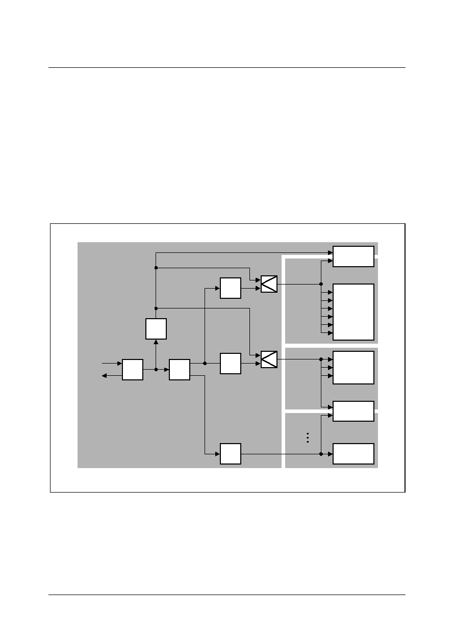
SDA 6000 / SDA 6001
PRELIMINARY DATA SHEET
Version 3.00
Clock System
8 - 4
Micronas
8.1
General Function
The on-chip clock generator provides M2 with its basic clock signals. Its oscillator can
either run with an external crystal and appropriate oscillator circuitry (refer to "Application
Diagram") or it can be driven by an external digital clock signal. For applications with low
accuracy requirements (RTC is not used) the external oscillator circuit can also be a
ceramic resonator. Depending on the absolute tolerance of the resonator the slicer may
not work correctly. Moreover the display timings and baud rate prescaler have to be
adapted in an appropriate way. In some applications the timing reference given by the
horizontal frequency of the CVBS signal can be used to measure the timing tolerance
and to adjust the programming.
Figure 8-1
Clock System in M2
The on-chip phase locked loop (PLL), which is internally running at 600 MHz, is fed by
the oscillator or can be bypassed to reduce the power consumption in idle and sleep
mode. If it is not required to wake up immediately from idle mode, the PLL can be
switched off by entering sleep-mode. The same oscillator is used to clock the built-in
RTC. (For a further description refer to Chapter 7.2.)
From the output frequency of the PLL three clock systems are derived:
3 MHz
300 MHz
DTO
SRU (part 2)
Display-FIFO
50 MHz
PIX
10 MHz
f
UES11167
DAC
6 MHz
XTAL2
XTAL1
OSC
� 2
PLL
200 MHz
( 3)
� 2
�
� 6
�
f
CPU
C-Periph.
Sync
Ports
Slicer
ADC
DG
EBI
CLUTs
100 MHz
EMI
66.7 MHz
f
3 MHz
33.33 MHz
C
�
RTC

SDA 6000 / SDA 6001
PRELIMINARY DATA SHEET
Version 3.00
Clock System
8 - 5
Micronas
One, the 33 MHz system clock (
f
CPU
) supplies the processor, all processor related
peripherals, the sync timing logic, the A/D converters and the slicer.
The second clock system (100/66 MHZ) (
f
EBI
) is used to clock the external bus interface,
the display generator, the CLUTs and the input part of the display FIFO. This clock starts
at 66 MHz after hardware reset. It can be configured to 100 MHz during the initialization
sequence.
The frequency of the latter clock system can be changed via bit CLKCON in register
SYSCON2. The refresh rate of the external SDRAM is always kept constant,
independent of the selected system clock frequency.
The third clock system runs the pixel clock (
f
PIX
), which is programmable in a range of
10 ... 50 MHz. It serves the output part of the display FIFO and the D/A converters. The
pixel clock is derived from the high frequency output of the PLL and it is phase shifted
line by line to the positive edge of the horizontal sync signal (normal polarity). Because
the final display clock is derived from a DTO (digital time oscillator) it has no equidistant
clock periods although the average frequency is exact. This pixel clock generation
system has several advantages:
� The frequency of the pixel clock can be programmed independently from the
horizontal line period.
� Since the input of the PLL is already a signal with a high frequency, the resulting pixel
frequency has an extremely low jitter.
� The resulting pixel clock follows the edge of the H-sync impulse without any delay and
always has the same quality as the sync timing of the deflection controller.

SDA 6000 / SDA 6001
PRELIMINARY DATA SHEET
Version 3.00
Clock System
8 - 6
Micronas
8.2
Register Description
SYSCON2 Reset
Value:
0000
H
Note: Register SYSCON2 cannot be changed after execution of the EINIT instruction.
PFR
Reset Value: 0148
H
Bit
Function
CLKCON
Bus Clock Frequency
0:
f
EBI
= 66 MHz
1:
f
EBI
= 100 MHz
Bit
Function
PF (10 ... 0)
Pixel Frequency Factor
This register defines the relation between the output pixel frequency and
the frequency of the crystal. The pixel frequency does not depend on the
line frequency. It can be calculated by the following formula:
The pixel frequency can be adjusted in steps of 36.6 KHz.
After power-on, this register is set to 328
D
. So, the default pixel
frequency is set to 12.01 MHz.
Note: Register values exceeding 1366 generate pixel frequencies
which are outside of the specified boundaries.
5
4
3
2
1
0
11
10
9
8
7
6
15
14
13
12
rw
1
-
-
-
-
-
CLK
CON
-
-
-
-
-
-
-
-
-
r
5
4
3
2
1
0
11
10
9
8
7
6
15
14
13
12
rw
-
-
-
-
-
-
PF(10..0)
f
PIX
= PF
�
300 MHz / 8192

Sync System

SDA 6000 / SDA 6001
PRELIMINARY DATA SHEET
Version 3.00
Sync System
9 - 3
Micronas
9
Sync System

SDA 6000 / SDA 6001
PRELIMINARY DATA SHEET
Version 3.00
Sync System
9 - 4
Micronas
9.1
General Description
The display sync system is completely independent of the acquisition sync system
(CVBS timing) and can either work as a sync master or as a sync slave system. Any
mention of "H/V-Syncs" in this chapter and in Chapter 10 always refers to display related
H/V Syncs and never to CVBS related sync timing.
In sync slave mode, M2 receives the synchronisation information from two independent
pins which deliver separate horizontal and vertical signals. Due to the not-line-locked
pixel clock generation (refer to Chapter 8), it can process any possible horizontal and
vertical sync frequency.
In sync master mode, M2 delivers separate horizontal and vertical signals with the same
flexibility in the programming of their periods as in sync slave mode.
9.1.1
Screen Resolution
The number of displayable pixels on the screen is defined by the pixel frequency (which
is independent of horizontal frequency), the line period and number of lines within a field.
The screen is divided into 3 different regions:
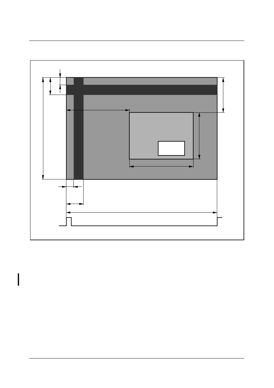
SDA 6000 / SDA 6001
PRELIMINARY DATA SHEET
Version 3.00
Sync System
9 - 5
Micronas
Figure 9-1
M2's Display Timing
Blacklevel Clamping Area
During horizontal and vertical blacklevel clamping, the black value (RGB = 000) is
delivered. The blank pin is set to `1' and COR is set to `0' (normal polarity assumed;
negative polarity is not allowed for COR and BLANK together with 3-level-output-pad).
This area is vertically programmable (in terms of lines) and horizontally in terms of
33.33 MHz clock cycles. These programmings are independent of all other registers.
Screen Background Area
The size of that area is defined by the sync delay registers (SDH and SDV) and the size
of pixel layer1. The contents of that area are defined by GA instruction SAR (refer also
to Chapter 10.1). Pixels within that area are programmable (colour and transparency
level), but all have the same value.
Layer 2
Pixel
(EHCR)
H_clmp_e
H-Sync
t
(BHCR)
H_clmp_b
t
H_period (HPR)
t
VLR
EVCR
BVCR
Screen Background Area
Vertical Blacklevel Clamping
(SDH)
Horizontal Blacklevel Clamping
H-Sync Delay
Variable Width
Pixel Layer 1
UET11168
V-Sync
Delay
(SDV)
Variable
Height

SDA 6000 / SDA 6001
PRELIMINARY DATA SHEET
Version 3.00
Sync System
9 - 6
Micronas
Pixel Layer Area
Pixels of this area are freely programmable according to the specifications of the display
generator. The information is stored in the frame buffer in the external memory, that
means the bigger that area is defined, the more bus performance is needed for SRU. If
that area is set to `0' no bus performance is needed. The start position of that area can
be shifted in horizontal and vertical direction by programming the horizontal and vertical
sync delay registers (SDH and SDV). The size of that area is defined by the instruction
FSR in the display generator.
Registers which allow the screen and sync parameters to be set up, are given in the
Table 9-1.
9.1.2
Sync Interrupts
The sync unit delivers interrupts (Horizontal and vertical interrupt) to the controller to
support the recognition of the frequencies of an external sync source (e.g. a VGA source
via SCART). These interrupts are related to the positive edge of the non delayed
horizontal and vertical impulses which can be seen at pins HSYNC and VSYNC.
Table 9-1
Overview on Sync Register Settings
Parameters
Register
Min Value Max
Value
Step
Default
Sync Control Register
SCR
see below
Sync Control Register 2
SCR2
see below
VL - Lines / Field
VLR
1 line
1024 lines 1 line
625 lines
T
h-period
- Horizontal Period
HPR
15
�
s
100
�
s
30 ns
64
�
s
F
pixel
- Pixel Frequency
PFR
10 MHz
50 MHz
73.25
KHz
12.01
MHz
T
vsync_delay
- Sync Delay
SDV
4 lines
1024 lines 1 line
32 lines
T
hsync_delay
- Sync Delay
SDH
32 pixel
2048 pixel 1 pixel
72 pixel
BVCR - Beginning
Of Vertical Clamp Phase
BVCR
1 line
1024 lines 1 line
line 1
EVCR - End Of
Of Vertical Clamp Phase
EVCR
1 line
1024 lines 1 line
line 5
T
h_clmp_b
- Beginning
Of Horizontal Clamp Phase
BHCR
0
�
s
163.2
�
s
480 ns
0
�
s
T
h_clmp_e
- End
Of Horizontal Clamp Phase
EHCR
0
�
s
163.2
�
s
480 ns
4.5
�
s

SDA 6000 / SDA 6001
PRELIMINARY DATA SHEET
Version 3.00
Sync System
9 - 7
Micronas
9.2
Register Description
SCR
Reset Value: 0000
H
Bit
Function
MAST
Master / Slave Mode
This bit defines the configuration of the sync system (master or slave
mode) and also the direction (input/output) of the V, H pins.
0:
Slave mode. H, V pins are configured as inputs.
1:
Master mode. H, V pins are configured as outputs.
Note: Switching from slave to master mode resets the internal H, V
counters, so that the phase shift during the switch can be
minimized. In slave mode registers VLR, and HPR are without any
use.
VCS
Vertical Composite Sync
VCS defines the sync output at pin V (Master mode only).
0:
At pin V the vertical sync appears.
1:
At pin V a composite sync signal (including equalizing pulses, H-
Sync and V-Syncs) is generated (VCS). The length of the
equalizing pulses have fixed values as described in the timing
specifications.
Note: Don't forget to set registers VLR and HPR according to your
requirements.
INT
Interlace / Non-interlace
M2 can either generate an interlaced or a non-interlaced timing. (Master
mode only). Interlaced timing can only be created if VLR is an odd
number.
0:
Interlaced timing is generated.
1:
Non-interlaced timing is generated.
VP
V-Pin Polarity
This bit defines the polarity of the V pin (master and slave mode).
0:
Normal polarity (active high).
1: Negative
polarity.
5
4
3
2
1
0
11
10
9
8
7
6
15
14
13
12
rw
rw
rw
rw
rw
rw
rw
rw
rw
FINV
DINT
VSU
(5)
VSU
(0)
COR-
BL
VSU(4..1)
BLAN
KP
COR
P
HP
VP
INT
VCS MAST
rw
rw
rw
rw

SDA 6000 / SDA 6001
PRELIMINARY DATA SHEET
Version 3.00
Sync System
9 - 8
Micronas
HP
H-Pin Polarity
This bit defines the polarity of the H pin. (Master and slave mode).
0:
Normal polarity (active high).
1: Negative
polarity.
CORP
COR-Pin Polarity
This bit defines the polarity of the COR pin. (Master and slave mode).
0:
Normal polarity (active high).
1:
Negative polarity (not allowed for CORBL = 1).
BLANKP
BLANK-Pin Polarity
This bit defines the polarity of the BLANK pin. (Master and slave mode).
0:
Negative polarity (not allowed for CORBL = 1).
1:
Normal polarity (active high).
VSU (5 ... 0) Vertical Set Up Time. (Master and slave mode)
The vertical sync signal is internally sampled at the next edge of the
horizontal sync plus a delay of
t
V_delay
. This is done because the phase
relation between V and H differs from application to application. To
guarantee (vertical) jitter free processing of external sync signals, the
sampling of the vertical sync impulse can be delayed before it is
internally processed. The following formula shows how to delay the
external V-sync before it is internally latched and processed.
t
V_delay
= 1.92
�
s
�
VSU(5...0)
CORBL
3-Level Contrast Reduction Output
There is one pin each for BLANK and COR. Nevertheless by means of
CORBL the user is able to switch the COR signal to a three level signal
providing BLANK and contrast reduction information on Pin BLANK
simultaneously.
0:
Two level signal for contrast reduction.
1: Three
level
signal
Level0: BLANK off; COR off.
Level1: BLANK off; COR on.
Level2: BLANK on; COR off.
Note: Please refer to Chapter 14 for the detailed specification of these
levels.
Bit
Function

SDA 6000 / SDA 6001
PRELIMINARY DATA SHEET
Version 3.00
Sync System
9 - 9
Micronas
DINT
Double Resolution for interlaced signals (Master and slave mode).
This bit is used to enable the double resolution feature for interlaced
video signals. If this feature is enabled the sync processing controls the
display unit in a different way. The display units splits the frame within
frame buffer into two fields (odd field/even field). For odd fields the odd
part of the frame is brought up to display and for even fields the even part
of the frame is brought up to display.
0:
Double Resolution for interlaced video signals is disabled
1:
Double Resolution for interlaced video signals is enabled
Note: If this feature is enabled bit0 (INT) within register SCR should be
set to interlaced (=0).
Note: This bit also controls the Screen Refresh Unit. The digital logic
inside Screen Refresh Unit which is controlled by this bit is only
available in SDA6001.
FINV
Field inversion for display unit (Master and slave mode).
Only used for silicon evaluation purposes. Should be kept in its original
state after reset.
Used to invert the field signal which is fed to the display unit in case the
double resolution feature for interlaced video signals is set enabled.
0:
Field signal is not inverted
1:
Field signal is inverted
Note: Also the bit SELP6.2 within the register ALTSELOP6 must be set
to 1 for enabling this function.
Bit
Function
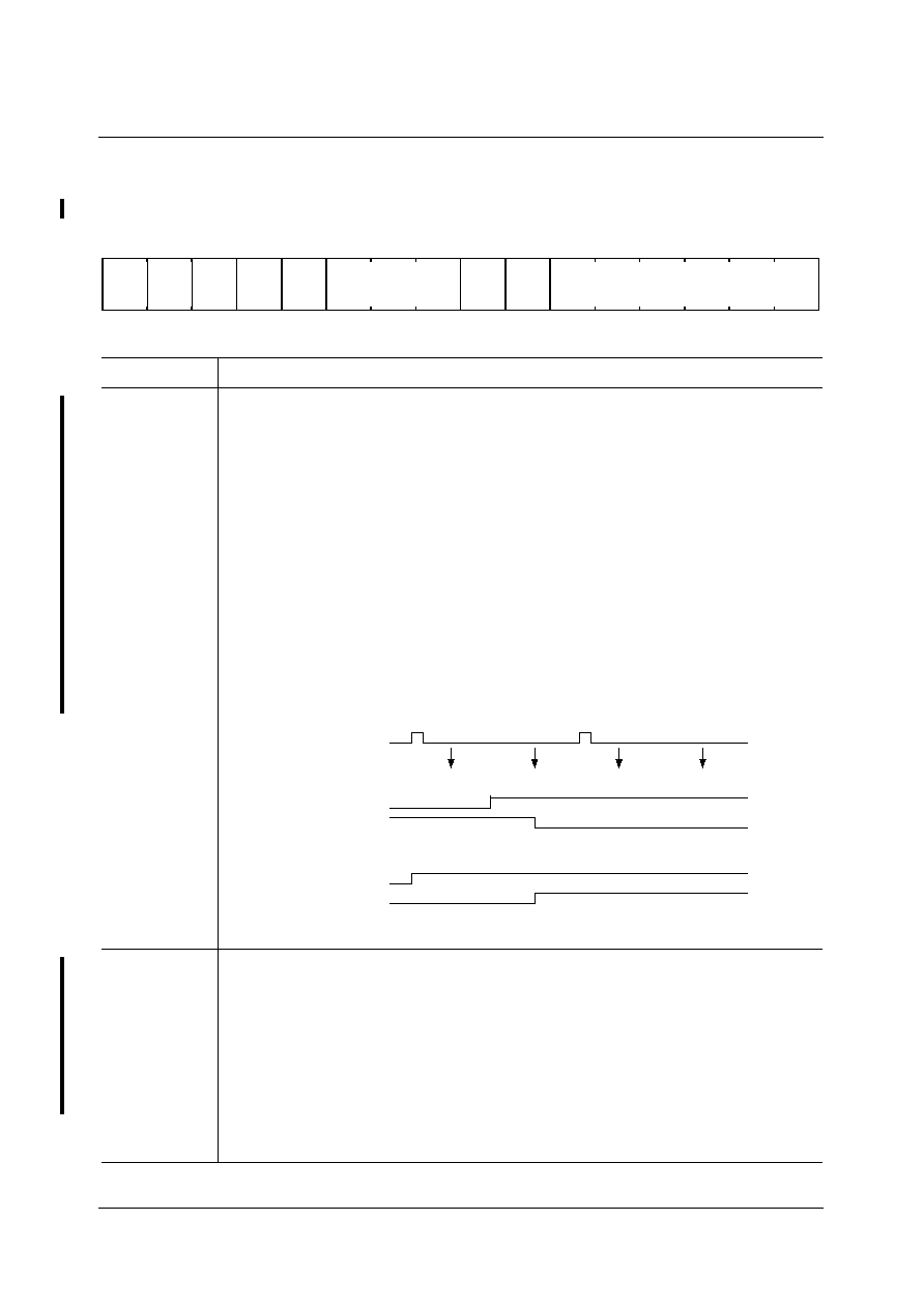
SDA 6000 / SDA 6001
PRELIMINARY DATA SHEET
Version 3.00
Sync System
9 - 10
Micronas
SCR2
Reset Value: 0011
H
Bit
Function
VSU2
Vertical Set Up Time 2 (Master and slave mode)
To realize the odd/even detection of a field next to VSU a second vertical
setup time VSU2 is defined by the VSU2 register bits. This horizontal
delay of VSU2 is used to recognize the Vsync at another time within the
video line than it is recognized at VSU. The field detection is based on
the fact that the phase-relationship of vertical and horizontal sync is
toggling from field to field for interlaced video signals.
t
V_delay2
= 1.92 us * VSU2
If VSYNC became active for both (VSU and VSU2), an odd field is
detected. If VSYNC became active only for VSU an even field is
detected:
FPORT
Field signal at port (Master and slave mode)
Used to enable the secondary function of Port6.2. If the secondary
function is enabled on this port the field signal of the field detection
appears.
0: Pin97 is used as Port6.2
1: Pin97 is used as output of the field detection
Note
5
4
3
2
1
0
11
10
9
8
7
6
15
14
13
12
rw
rw
rw
rw
rw
rw
rw
-
-
FPOR
T
-
-
-
FOFF_ALPHA
FDET
E
VSU2 (5...0)
rw
r
HSync
VSync (B)
VSync (A)
field-signal
field-signal
VSU2
VSU
VSU2
VSU

SDA 6000 / SDA 6001
PRELIMINARY DATA SHEET
Version 3.00
Sync System
9 - 11
Micronas
FDETE
Field detection (Master and slave mode)
This bit is written by the field detection hardware.
0: odd field has been detected by the field detection
1: even field has been detected by the field detection
FOFF_ALPH
A
Alpha raster offset (Master and slave mode)
Only used if the double resolution mode for interlaced signals is enabled
(register SCR/Bit DINT).
These bits are used to generate a offset of alpha raster in relation to beta
raster. These bits are only used for evaluation purpose. For normal
operation they should be kept in their initial state.
011: Offset set to +3 lines
010: Offset set to +2 lines
001: Offset set to +1 line
000: Offset set to 0 line
111: Offset set to -1 line
110: Offset set to -2 lines
101: Offset set to -3 lines
100: Offset set to -4 lines
Bit
Function
SDA 6000 / SDA 6001
PRELIMINARY DATA SHEET
Version 3.00
Sync System
9 - 12
Micronas
VLR
Reset Value: 0271
H
HPR
Reset Value: 855
H
Bit
Function
VLR (9 ... 0) Amount of Vertical Lines in a Frame. (Master mode only).
M2 generates vertical sync impulses in sync master mode. If, for
example, a normal PAL timing should be generated, set the register to
`625d' and set the interlace bit to `0'. The hardware will generate a
vertical impulse periodically after 312.5 lines. If a non-interlaced picture
with 312 lines should be generated, set this register to `312' and set the
interlace bit to `1'. The hardware will generate a vertical impulse every
312 lines. Progressive timing can be generated by setting VLR to `625'
and interlace to `1'.
Bit
Function
HPR
(11 ... 0)
Horizontal Period factor. (Master mode only)
This register allows the period of the horizontal sync signal to be
adjusted. The horizontal period is independent of the pixel frequency and
can be adjusted with the following resolution:
5
4
3
2
1
0
11
10
9
8
7
6
15
14
13
12
rw
-
-
-
-
-
-
VL(9..0)
5
4
3
2
1
0
11
10
9
8
7
6
15
14
13
12
rw
-
-
-
-
HP(11..0)
t
H-period
= HP
�
30 ns
SDA 6000 / SDA 6001
PRELIMINARY DATA SHEET
Version 3.00
Sync System
9 - 13
Micronas
SDV
Reset Value: 0020
H
SDH
Reset Value: 0020
H
Bit
Function
SDV (9 ... 0) Vertical Sync Delay. (Master and slave mode).
This register defines the delay (in lines) from the vertical sync to the first
line of pixel layer 1 on the screen.
Bit
Function
SDH
(11 ... 0)
Horizontal Sync Delay. (Master and slave mode).
This register defines the delay (in pixels) from the horizontal sync to the
first pixel of layer 1 on the screen.
5
4
3
2
1
0
11
10
9
8
7
6
15
14
13
12
rw
-
-
-
-
-
-
SDV(9..0)
5
4
3
2
1
0
11
10
9
8
7
6
15
14
13
12
rw
-
-
-
-
SDH

SDA 6000 / SDA 6001
PRELIMINARY DATA SHEET
Version 3.00
Sync System
9 - 14
Micronas
HCR
Reset Value: 0A00
H
The clamp phase area has higher priority than the screen background area or the pixel
layer area and can be shifted independent from any other register.
Bit
Function
BHCR
(7 ... 0)
Beginning of Horizontal Clamp Phase. (Master and slave mode).
This register defines the delay of the horizontal clamp phase from the
positive edge of the horizontal sync impulse (normal polarity is
assumed). The beginning of the clamp phase can be calculated by the
following formula:
t
H_clmp_b
= 480 ns
�
BHCR
EHCR
(7 ... 0)
End of Horizontal Clamp Phase. (Master and slave mode).
This register defines the end of the horizontal clamp phase from the
positive edge of the horizontal sync impulse (at normal polarity). The end
of the clamp phase can be calculated by the following formula:
t
H_clmp_e
= 480 ns
�
EHCR
If EHCR is smaller than BHCR the clamp phase will include the H-sync
phase.
5
4
3
2
1
0
11
10
9
8
7
6
15
14
13
12
rw
rw
EHCR(7..0)
EHCR(7..0)
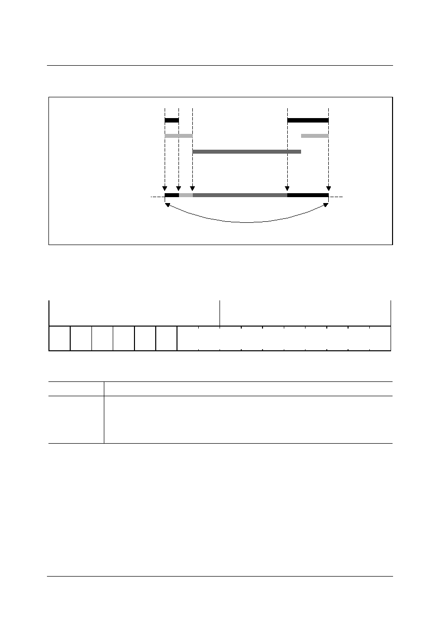
SDA 6000 / SDA 6001
PRELIMINARY DATA SHEET
Version 3.00
Sync System
9 - 15
Micronas
Figure 9-2
Priority of Clamp Phase, Screen Background and Pixel Layer Area
BVCR
Reset Value: 0000
H
Bit
Function
BVCR
(9 ... 0)
Beginning of Vertical Clamp Phase. (Master and slave mode).
This register defines the beginning of the vertical clamp phase from the
positive edge of the vertical sync impulse (at normal polarity) in line
count.
UED11169
Clamp Phase Area
Screen Background Area
Pixel Layer Area
Video
H Period - Frame n
H Pulse
rw
-
-
-
-
-
-
BVCR(9..0)
5
4
3
2
1
0
7
6
BVCR0
BVCR1
11
10
9
8
15
14
13
12

SDA 6000 / SDA 6001
PRELIMINARY DATA SHEET
Version 3.00
Sync System
9 - 16
Micronas
EVCR
Reset Value: 000A
H
Bit
Function
EVCR
(9 ... 0)
End of Vertical Clamp Phase. (Master and slave mode).
This register defines the end of the vertical clamp phase from the positive
edge of the vertical sync impulse (at normal polarity) in line count.
Note: It must be guaranteed that the value EVCR is always smaller than
the value of SDV.
rw
-
-
-
-
-
-
EVCR(9..0)
5
4
3
2
1
0
7
6
EVCR0
EVCR1
11
10
9
8
15
14
13
12

SDA 6000 / SDA 6001
PRELIMINARY DATA SHEET
Version 3.00
Sync System
9 - 17
Micronas
9.3
Double Resolution combined with interlaced video signals Ionly
SDA6001)
This chapter describes in which way the double resolution synchronisation for interlaced
video signals is implemented within SDA6001 since design step B11.
For this the different existing 50Hz/100Hz sync rasters and the different modes are
described.
Furthermore it's described which registers are of special interest for the double
resolution mode.
In a last chapter some details of the design are described.
9.3.1
Sync rasters
For interlaced sync rasters a original progressive frame is divided into two fields before
it is brought up to display - an odd field (odd lines of the original progressive frame) and
an even field (even lines of the original progressive frame). These fields are also called
fieldA and fieldB.
For all the different 50 Hz and 100Hz modes field A is always displayed in display raster
alpha and field B is always displayed in display raster beta.
Which raster (alpha or beta) shows up line by line on the screen depends on the phase
relationship of the HSyncs and the VSyncs. For this within the M2 redesign a field
detection will be implemented within the sync seperation circuit.
In principle the different modes (ABAB, AABB, AAAA) of 100Hz displays don't have any
impact on the hardware needed for the double resolution feature. Those modes were just
added to this document to have the complete view for all involved people and to avoid
missunderstandings.
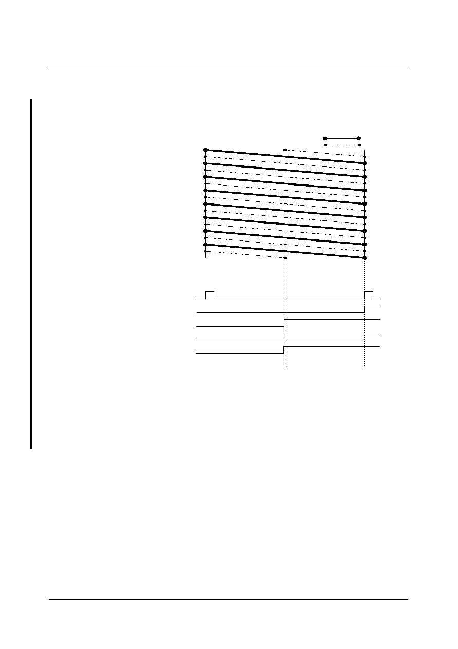
SDA 6000 / SDA 6001
PRELIMINARY DATA SHEET
Version 3.00
Sync System
9 - 18
Micronas
9.3.1.1
50Hz/100Hz Mode (ABAB)
Figure 9-3
50Hz/100Hz mode(ABAB)
Regarding the shape of the sync signals the 100Hz(ABAB) mode is directly comparable
with the 50Hz mode. The only difference of the 50Hz and the 100Hz mode (ABAB) is
the frequency itself. This mode drastically reduces the interline flickering by transfering
the flicker frequency from the human visible frequency of 25Hz to the human less visible
frequency of 50Hz.
H-Sync
alpha
beta
prog.
alpha
beta
0
0
1
0
2
1
3
1
4
2
5
2
6
3
7
3
8
4
9
4
10
5
11
5
12
6
13
6
14
7
.......
V-Sync 1st field
V-Sync 2nd field
V-Sync 3rd field
V-Sync 4th field
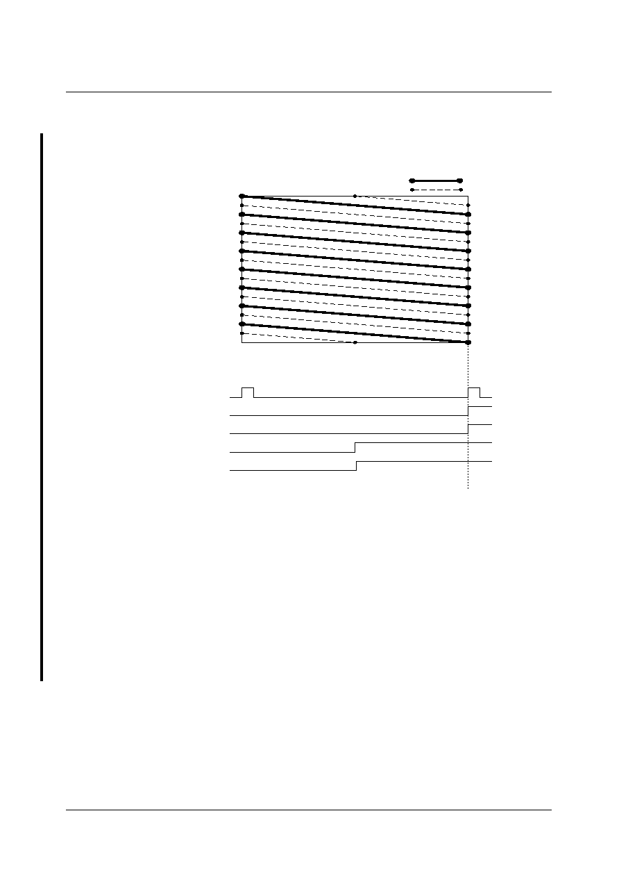
SDA 6000 / SDA 6001
PRELIMINARY DATA SHEET
Version 3.00
Sync System
9 - 19
Micronas
9.3.1.2
100 Hz Mode (AABB)
Figure 9-4
100 Hz Mode (AABB)
This mode shows on the screen still the interline flickering known from 50Hz modes.
Each single field is drawn within 20ms two times and afterwards the next field is drawn
two times.
ATTENTION: If OSD is displayed with double vertical resolution, the interline flickering
- wellknown from 50Hz systems - will appear in this mode. If the 100Hz up conversion
unit changes automatically between this mode and the mode "ABAB" flickering will
appear and disappear time by time.
alpha
beta
prog.
alpha
beta
0
0
1
0
2
1
3
1
4
2
5
2
6
3
7
3
8
4
9
4
10
5
11
5
12
6
13
6
14
7
.......
V-Sync 1st field
V-Sync 2nd field
V-Sync 4th field
V-Sync 3rd field
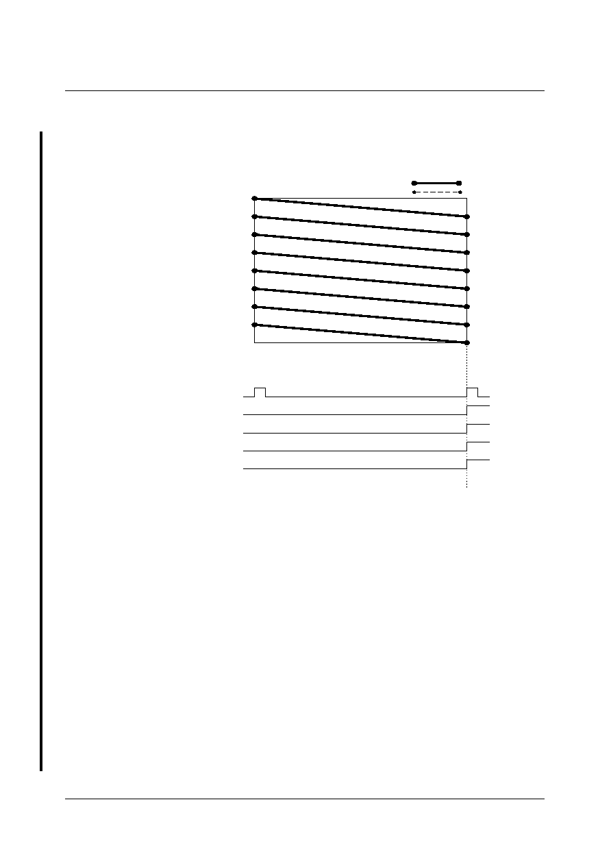
SDA 6000 / SDA 6001
PRELIMINARY DATA SHEET
Version 3.00
Sync System
9 - 20
Micronas
9.3.1.3
100 Hz Mode (AAAA)
Figure 9-5
100 Hz Mode (AAAA)
9.3.2
Registers important for double resolution
Herein those registers are shortly summarized which are important to control the double
resolution feature. This summary intends to put readers attention especially to those
registers. For a more detailed description of these registers please see Chapter 9.2.
� register SCR
position FINV
� register SCR
position DINT (only available in SDA6001)
� register SCR2
position VSU2
� register SCR2
position FPORT
� register SCR2
position FDETE
� register SCR2
position FOFF_ALPHA
� register SCR
position VSU
H-Sync
alpha
beta
prog.
alpha
beta
0
0
1
0
2
1
3
1
4
2
5
2
6
3
7
3
8
4
9
4
10
5
11
5
12
6
13
6
14
7
.......
V-Sync 1st field
V-Sync 2nd field
V-Sync 4th field
V-Sync 3rd field
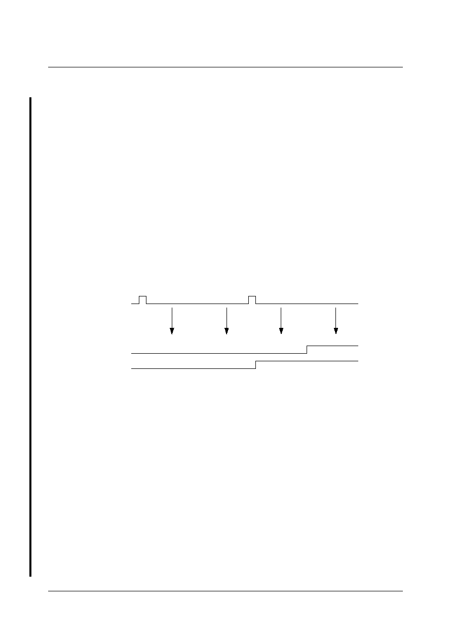
SDA 6000 / SDA 6001
PRELIMINARY DATA SHEET
Version 3.00
Sync System
9 - 21
Micronas
9.3.3
Implementation details
There are two functionalities implemented to allow the display of double resolution
graphics on a interlaced video signal:
1. field detection within sync seperation
2. fieldwise read sequence of the progressive frame from frame buffer.
9.3.3.1
Field detection
The Screen Refresh Unit of SDA6000 needs a signal which indiactes if the following field
is drawn in display raster alpha or display raster beta. Using this field information its
decided which field information of the progressive frame is read from the memory and
brought to display.
The fieldinformation is generated by use of the phase relationship of Vsync to Hsync. For
this within each single line the Vsync signal is sampled one time at the position VSU and
one time at the position VSU2.
Figure 9-6
Sampling of VSync for field detection
So the optimum sampling time for VSU2 is 48us(50Hz)/24us(100Hz) and for VSU the
optimum sampling time is 16us(50Hz)/8us(100Hz).
Practically there is a offset of t
delay
which make the Vsync appear after
32us(50Hz)/16us(100Hz) + t
delay
or
0us + t
delay
in relation to the Hsync.
t
delay
differs from one TV chassis to another TV chassis. Only the TV set manufacturer
itself knows this parameter. So each TV set manufacturer must be able to adapt the field
detection to his needs on one side, and also for the different settings for 50Hz and 100Hz
systems the sampling times VSU and VSU2 must be flexible on the other side.
For this, two registers VSU and VSU2 are used (see also 2.2). These registers allow to
setup the sample time in steps of 1.92us.
VSU2
VSU
VSU
VSU2
HSync
VSync (alpha)
VSync (beta)
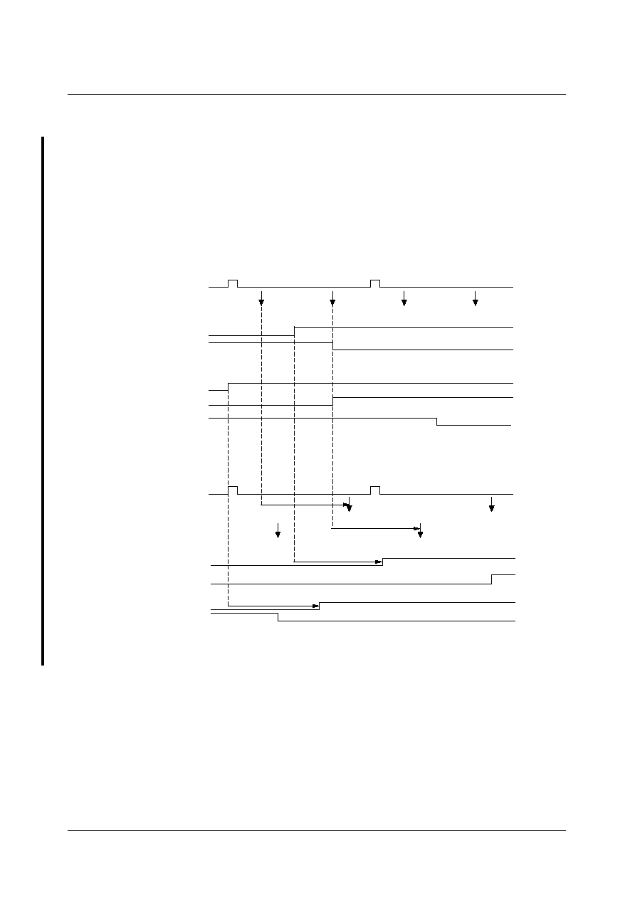
SDA 6000 / SDA 6001
PRELIMINARY DATA SHEET
Version 3.00
Sync System
9 - 22
Micronas
For t
delay
>32us another problem occures:
As shown in the figures below, for delays >32us the field signal becomes inverted. To
allow TV set manufacturers to compensate this inversion a additional register FINV is
implemented. If FINV is set to high the field signal is inverted before it is used for further
processing.
Figure 9-7
Sampling of VSync for field detection in case of delayed VSyncs
HSync
VSync (B)
VSync (A)
field-signal
field-signal
HSync
VSync (B)
VSync (A)
field-signal
field-signal
VSU2
VSU
t
delay
>32us
t
delay
>32us
Scenario1 t
delay
=0us:
Scenario1 t
delay
=32us:
VSU2
VSU
VSU2
VSU
t
delay
>32us
VSU
t
delay
>32us
VSU2

SDA 6000 / SDA 6001
PRELIMINARY DATA SHEET
Version 3.00
Sync System
9 - 23
Micronas
9.3.3.2
Splitting of the frames(Layer1/Layer2) within frame buffer to
display raster
The double resolution feature automatically splits the progressive frame inside the frame
buffer of SDA6000 into two different fields. In the register SDV[9..0] the vertical offset of
the layers is adjusted. Depending on the settings of SDV the two different fields (A/B) of
the progressive frame within the frame buffers belong one time to the alpha raster and
one time to the beta raster if SDV is decremented or incremented.
Figure 9-8
Position of Layer1/Layer2 within the display raster
The progressive frame of the Layer1 and Layer2 within frame buffer must be split to field
A and field B as follows. In the figure below field A is assigned to display raster alpha and
field B is assigned to display raster beta:
progr. raster
raster
(alpha) (beta)
0
0
1
0
2
1
3
1
4
2
5
2
6
3
7
3
8
4
0
4
10
5
11
5
12
6
13
6
14
7
15
7
16
8
17
8
18
9
19
9
20
10
21
10
22
11
23
11
24
12
25
12
26
13
27
13
28
14
29
14
30
15
31
15
display raster
alpha
display raster
beta
SDV
Layer 2
Layer 1

SDA 6000 / SDA 6001
PRELIMINARY DATA SHEET
Version 3.00
Sync System
9 - 24
Micronas
Figure 9-9
Splitting of the frames (Layer1/Layer2) to the display raster
If SDV is incremented by one, the following, different scenario appears. For this, the
assignment of fieldA and fieldB within the progressive frame in frame buffer must be
inverted, so that again fieldA can be displayed within display raster alpha and fieldB can
be displayed within display raster beta:
Figure 9-10 Position of Layer1/Layer2 within the display raster
Layer 2:
A
B
A
B
A
B
A
B
A
B
A
B
A
B
A
Layer 1:
B
A
B
A
B
A
B
A
B
A
B
A
B
A
B
A
B
A
B
A
B
progr. raster
raster
(alpha) (beta)
0
0
1
0
2
1
3
1
4
2
5
2
6
3
7
3
8
4
9
4
10
5
11
5
12
6
13
6
14
7
15
7
16
8
17
8
18
9
19
9
20
10
21
10
22
11
23
11
24
12
25
12
26
13
27
13
28
14
29
14
30
15
31
15
display raster
alpha
display raster
beta
SDV+1
Layer 2
Layer 1

SDA 6000 / SDA 6001
PRELIMINARY DATA SHEET
Version 3.00
Sync System
9 - 25
Micronas
Figure 9-11 Splitting of the frames (Layer1/Layer2) to the display raster
Layer 2:
B
A
B
A
B
A
B
A
B
A
B
A
B
A
B
Layer 1:
A
B
A
B
A
B
A
B
A
B
A
B
A
B
A
B
A
B
A
B
A

Display Generator

SDA 6000 / SDA 6001
PRELIMINARY DATA SHEET
Version 3.00
Display Generator
10 - 3
Micronas
10
Display Generator

SDA 6000 / SDA 6001
PRELIMINARY DATA SHEET
Version 3.00
Display Generator
10 - 4
Micronas
10.1
General Description
M2's display concept is based on frame buffer technology, which means that for each
pixel displayed on a screen appropriate information is stored in the memory of the so
called frame buffer. To relieve the controller from processing time consuming tasks like
writing this frame buffer pixel by pixel, a graphic accelerator machine is introduced (GA).
The GA reads e.g. bitmap information in various formats together with attributes which
define the final behavior of those bitmaps. Depending on these attributes these bitmaps
are processed and written into the frame buffer. Due to the processor like architecture of
the GA, it is controlled by so called GAIs (graphic accelerator instructions). The screen
refresh unit (SRU) reads out the pixel based information (various formats are also
available here) and hands them over via a look up table and a FIFO to the D/A converter.
The FIFO is used to adapt the variable pixel output frequency to the fixed memory bus
frequency. Up to two frame buffers are possible and supported by GA and SRU.

SDA 6000 / SDA 6001
PRELIMINARY DATA SHEET
Version 3.00
Display Generator
10 - 5
Micronas
10.2
Screen Alignments
Two HW-layers are supported: layer 1 and layer 2. Layer 2 can be positioned relative to
layer 1 (also in negative direction). If layer 2 exceeds the dimensions of layer 2 these
exceeding parts are not visible on the screen.
The alignment of the OSD on the screen depends on the configuration of layer 1.
The maximum amount of displayable pixels is 2047 pixels in horizontal direction and
1023 pixels in vertical direction.

SDA 6000 / SDA 6001
PRELIMINARY DATA SHEET
Version 3.00
Display Generator
10 - 6
Micronas
To adapt M2 to a wide range of displays in the market the sync-processing can be flexibly
configured.
Figure 10-1 Display Regions and Alignments
There are three registers in the synchronization unit which are necessary for OSD setup:
� SDH: used to setup the horizontal position of the top left pixel of layer 1.
� SDV: used to setup the vertical position of the top left pixel of layer 1.
� PFR: used to setup the pixel frequency.
For detailed description of these registers please refer to chapter `Display Sync System'
and `Clock System'.
In the area which is defined for layer 1 or layer 2 (layer area) each pixel is defined by the
attribute definition of the frame buffer. There is no pixel by pixel definition for the
blacklevel clamping area and the screen background area. For these areas the colour
and transparency is defined as follows:
Transparency level and colour of the screen background area is defined globally for the
whole screen by GA instruction SAR.
During the blacklevel clamping area, black value (RGB = `000') is delivered at RGB
output. Pin `Blank' is set to `1' and COR-pin is set to `0' (normal polarity is assumed).
UED11170
Horizontal Blacklevel Clamping
Vertical Blacklevel Clamping
Screen Background Area
Height
Variable
Variable Width
Layer 1
Area
Area
Non-Visible Part
of Layer 2
Layer 2
SDA 6000 / SDA 6001
PRELIMINARY DATA SHEET
Version 3.00
Display Generator
10 - 7
Micronas
10.3
Layer Concept
M2 supports two HW-layers. Frame buffers of layer 1 and layer 2 can be placed at any
word aligned position in external memory.
Two different layer modes can be chosen:
� Overlapped layers. Layer 1 and layer 2 are processed in parallel by the screen refresh
unit.
� Embedded layers. Layer 1 and layer 2 are alternatively processed.
If the area of layer 2 exceeds the area of layer 1, these parts are not visible on the screen.
Mixing of layer 1 and layer 2 is performed by the display generator. As a result of the
RGB output of M2, there is only one RGB stream which contains the information of layer
1 and layer 2. This RGB stream is externally mixed with a video source. For this external
mixing there are two output signals (COR and BLANK) available.
Meshed areas:
A special mesh mode is defined to mix the external video with the RGB information from
M2 in a chess-pattern-shape. From frame to frame this chess-pattern is inverted.
Inverted means, that pixels which have been displayed as video in the previous frame,
are displayed as RGB in the following frame.
Figure 10-2 Behavior of Blank Pin for Consecutive Frames in `Meshed' Regions
UEA11171
t
t
+1
+2
t
Blank = 1; External Video
Blank = 0; RGB of M2
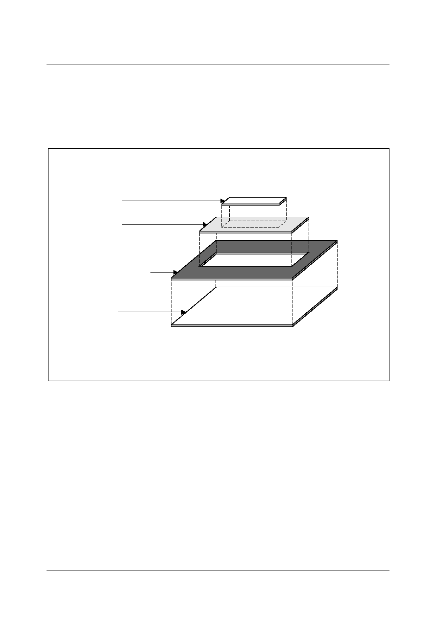
SDA 6000 / SDA 6001
PRELIMINARY DATA SHEET
Version 3.00
Display Generator
10 - 8
Micronas
10.3.1
Overlapped Layers
In overlapped layer mode the pixel information of both layers (layer 1, layer 2) is read in
parallel to the RAM. This means that for each pixel the individual decision can be made
which pixel source (layer 1, layer 2, screen background or video) has the highest priority.
Figure 10-3 Priority of Layers in Overlapped Layer Mode
The transparency between layers is supported. Below layer 2 there is layer 1, below
layer 1 there is the screen background colour and below screen background there is
video. In overlapped layer mode a transparency hierarchy is defined for layer 2, layer 1,
screen background and video. The transparency hierarchy is controlled, for each pixel,
by two bits (TR1 ... 0) which are defined in the pixel format of the framebuffer and bit
SBTL which is defined in instruction SAR. Thus each pixel position can be defined
individually as layer 1, layer 2, screen background, video or contrast reduced video.
Depending on the transparency bits of both layers, subsequent signals are switched to
the RGB, COR and BLANK (normal polarity assumed) outputs of M2. As a result one of
the two layers or the screen background will be visible on the screen. If layer 2 is not
available for a pixel, signals COR, BLANK and RGB output depends on layer 1 only.
UEA11172
Layer 2
Layer 1
Background Color
Video

SDA 6000 / SDA 6001
PRELIMINARY DATA SHEET
Version 3.00
Display Generator
10 - 9
Micronas
Table 10-1
Behavior of M2's Outputs in Overlapped Layer Mode
Layer 1
Layer 2
Screen
Background
BLANK
Pin
COR
Pin
RGB
Pins
RGB
Tube
TR1
TR0
TR1
TR0
SBTL
0
0
n.a.
*1)
n.a.
0
0
0
Layer 1
Layer 1
0
1
n.a.
n.a.
0
Meshed
0
Layer 1
Layer 1/
Video
1
0
n.a.
n.a.
0
0
0
Back-
ground
Back-
ground
1
1
n.a.
n.a.
0
0
0
Back-
ground
Back-
ground
X
*2)
X
0
0
0
0
0
Layer 2
Layer 2
X
X
0
1
0
Meshed
0
Layer 2
Layer 2/
Video
0
0
1
X
0
0
0
Layer 1
Layer 1
0
1
1
X
0
Meshed
0
Layer 1
Layer 1/
Video
1
0
1
X
0
0
0
Back-
ground
Back-
ground
1
1
1
X
0
0
0
Back-
ground
Back-
ground
0
0
n.a.
n.a.
1
0
0
Layer 1
Layer 1
0
1
n.a.
n.a.
1
Meshed
0
Layer 1
Layer 1/
Video
1
0
n.a.
n.a.
1
1
0
Back-
ground
Video
1
1
n.a.
n.a.
1
1
1
Back-
ground
Contrast
red. Video
X
X
0
0
1
0
0
Layer 2
Layer 2
X
X
0
1
1
Meshed
0
Layer 2
Layer 2/
Video
0
0
1
X
1
0
0
Layer 1
Layer 1
0
1
1
X
1
Meshed
0
Layer 1
Layer 1/
Video

SDA 6000 / SDA 6001
PRELIMINARY DATA SHEET
Version 3.00
Display Generator
10 - 10
Micronas
*1)
n.a. = not available
*2)
X = don't care
For transparency in `screen background area' please refer to Chapter 10.3.3.
10.3.2
Embedded Layers
Layer 1 and 2 are not read in parallel to the RAM. The SRU reads only one layer at a
time. During the area of layer 2 only pixels of layer 2 are read. Otherwise only layer 1 is
read. As a result in the area of layer 2, the pixel information for layer 1 is not available.
This is why layer 2 is transparent to video and not to layer 1. As a result, in embedded
layer mode, transparency between layers is only supported layer-wise not pixel-wise.
Also please refer to transparency using overlapped layers (Chapter 10.3.1).
1
0
1
X
1
1
0
Back-
ground
Video
1
1
1
X
1
1
1
Back-
ground
Contrast
red. Video
Table 10-1
Behavior of M2's Outputs in Overlapped Layer Mode (cont'd)
Layer 1
Layer 2
Screen
Background
BLANK
Pin
COR
Pin
RGB
Pins
RGB
Tube
TR1
TR0
TR1
TR0
SBTL
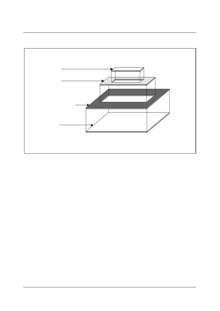
SDA 6000 / SDA 6001
PRELIMINARY DATA SHEET
Version 3.00
Display Generator
10 - 11
Micronas
.
Figure 10-4 Priority of Layers in Embedded Layer Mode
Depending on the transparency bits of both layers, the following signals are switched to
the RGB, COR and BLANK (normal polarity assumed) outputs of M2. As a result, one of
the two layers or the screen background will be visible on the screen. If layer 2 is not
available for a pixel, signals COR, BLANK and RGB output depends only on layer 1.
The transparency hierarchy is again controlled, for each pixel, by two bits (TR1 ... 0)
which are defined in the pixel format. On the RGB output of M2 there is a mix of layer 1
and layer 2 RGB stream with the screen background.
Depending on the transparency bits of one of the layers subsequent signals are switched
to RGB, COR and BLANK (normal polarity assumed).
The output signals of M2 (COR, BLANK, RGB) depend only on transparency bits of layer
1 or on layer 2 and never on both layers because there is no pixel position where both
layers are available in parallel.
10.3.3
Transparency in Screen Background Area
Depending on the height and width definition of layer 1 there is a remaining portion of
visible screen area without any pixel definition of layer 1 or layer 2. For this area the
transparency bits for layer 1 and layer 2 are not available. For this `Screen Background
Area' the colour attributes and transparency attributes are globally defined for the whole
screen. Also refer to instruction SAR described in Chapter 10.7.1.
UEA11173
Layer 2
Layer 1
Background Color
Video

SDA 6000 / SDA 6001
PRELIMINARY DATA SHEET
Version 3.00
Display Generator
10 - 12
Micronas
Table 10-2
Behavior of M2's Outputs in Embedded Layer Mode
Layer 1
Layer 2
Screen
Back-
ground
BLANK
Pin
COR
Pin
RGB
Pins
RGB
Tube
TR1
TR0
TR1
TR0
SBTL
0
0
n.a.
n.a.
0
0
0
Layer 1
Layer 1
0
1
n.a.
n.a.
0
Meshed
0
Layer 1
Layer 1 /
Video
1
0
n.a.
n.a.
0
0
0
Back-
ground
Back-
ground
1
1
n.a.
n.a.
0
0
0
Back-
ground
Back-
ground
n.a.
n.a.
0
0
0
0
0
Layer 2
Layer 2
n.a.
n.a.
0
1
0
Meshed
0
Layer 2
Layer 2 /
Video
n.a.
n.a.
1
0
0
0
0
Back-
ground
Back-
ground
n.a.
n.a.
1
1
0
0
0
Back-
ground
Back-
ground
0
0
n.a.
n.a.
1
0
0
Layer 1
Layer 1
0
1
n.a.
n.a.
1
Meshed
0
Layer 1
Layer 1 /
Video
1
0
n.a.
n.a.
1
1
0
Back-
ground
Video
1
1
n.a.
n.a.
1
1
1
Back-
ground
Contrast
red. Video
n.a.
n.a.
0
0
1
0
0
Layer 2
Layer 2
n.a.
n.a.
0
1
1
Meshed
0
Layer 2
Layer 2 /
Video
n.a.
n.a.
1
0
1
1
0
Back-
ground
Video
n.a.
n.a.
1
1
1
1
1
Back-
ground
Contrast
red. Video

SDA 6000 / SDA 6001
PRELIMINARY DATA SHEET
Version 3.00
Display Generator
10 - 13
Micronas
Table 10-3
Behavior of M2's Outputs in Background Area
Screen
Background
BLANK
Pin
COR
Pin
RGB Pins
RGB Tube
STR1
STR0
0
0
0
0
RGB values
defined in SAR
RGB values defined
in SAR
0
1
Meshed
0
RGB values
defined in SAR
RGB values defined
in SAR/Video
1
0
1
0
RGB values
defined in SAR
Video
1
1
1
1
RGB values
defined in SAR
Contrast red. Video

SDA 6000 / SDA 6001
PRELIMINARY DATA SHEET
Version 3.00
Display Generator
10 - 14
Micronas
10.4
Input and Output Formats
The transfer of one memory area to another is executed by the graphic accelerator (GA).
Transfer means reading data from a source memory area in a given input format,
modifying the data and writing it in a defined output format to the destination memory
area. Different input and output formats are supported:
Note:
1)
The 2-bit format is defined as a format for the frame buffer but not supported by
the GA.
Table 10-4
Overview on Formats
Input Formats
Output Formats
1-bit bitmap
2-bit format CLUT2 vector
1)
2-bit bitmap
8-bit format CLUT2 vector
4-bit bitmap
16-bit format (4:4:4:2) RGB
8-bit bitmap
16-bit format (TTX) CLUT2 vector
8-bit data (for direct data transfer)
16-bit format (5:6:5) RGB
CLUT1 input
8-bit data (for direct data transfer)
16-bit format (4:4:4:2)
�
SDA 6000 / SDA 6001
PRELIMINARY DATA SHEET
Version 3.00
Display Generator
10 - 15
Micronas
10.4.1
Input Formats
The following figures describe how bitmaps for different input bit map formats are stored
in the source memory area . The 16-bit format is described in Figure 10-12.
Figure 10-5 Format of 1-bitplane Bitmap
Note: The 1-bitplane format is used to address vectors 1 ... 0 of CLUT1.
Figure 10-6 Format of 2-bitplane Bitmap
Note: The 2-bitplane format is used to address vectors 3 ... 0 of CLUT1.
Figure 10-7 Format of 4-bitplane Bitmap
Note: The 4-bitplane format is used to address vectors 15 ... 0 of CLUT1.
UED11174
Memory Addr. = n
Memory Addr. = n+2
bit_1
bit_5
bit_7 bit_6
bit_3
Byte Address n+1
bit_4
bit_2
bit_1
bit_5
Byte Address n
bit_7
bit_0
bit_6
bit_3
bit_4
bit_2
bit_0
Byte Address n+3
Byte Address n+2
14
Pixel
10
Pixel
8
Pixel
9
Pixel
12
Pixel
11
Pixel
13
Pixel
6
Pixel
2
Pixel
0
Pixel
15
Pixel
1
Pixel
4
Pixel
3
Pixel
5
Pixel
7
Pixel
30
Pixel
Pixel
26
24
Pixel
25
Pixel
28
Pixel
Pixel
27
Pixel
29
22
Pixel
18
Pixel
16
Pixel
Pixel
31
17
Pixel
20
Pixel
19
Pixel
21
Pixel
23
Pixel
UED11175
Memory Addr. = n+2
Memory Addr. = n
13/Bit1
Pixel/
Pixel
12/Bit0
Pixel
12/Bit1
Pixel/
13/Bit0
Pixel
14/Bit1
Pixel
14/Bit0
Pixel
15/Bit1
Pixel
15/Bit0
Pixel
8/Bit1
Pixel
8/Bit0
Pixel
9/Bit1
Pixel
9/Bit0
Pixel
10/Bit1
Pixel
10/Bit0
Pixel
11/Bit1
Pixel
11/Bit0
3/Bit1
Pixel
1/Bit1
Pixel
0/Bit1
Pixel
0/Bit0
Pixel
2/Bit1
Pixel
1/Bit0
Pixel
2/Bit0
Pixel
3/Bit0
Pixel
7/Bit1
Pixel
Pixel
5/Bit1
4/Bit1
Pixel
4/Bit0
Pixel
6/Bit1
Pixel
Pixel
5/Bit0
Pixel
6/Bit0
Pixel
7/Bit0
Byte Address n+1
Byte Address n+3
Byte Address n+2
Byte Address n
bit_7 bit_6 bit_5 bit_4 bit_3 bit_2 bit_1 bit_0 bit_7 bit_6 bit_5 bit_4 bit_3 bit_2 bit_1 bit_0
UED11176
Memory Addr. = n+2
Memory Addr. = n
6/Bit1
Pixel
Pixel
6/Bit2
Pixel
6/Bit3
Pixel
6/Bit0
Pixel
7/Bit3
Pixel
7/Bit2
Pixel
7/Bit1
Pixel
7/Bit0
Pixel
4/Bit3
Pixel
4/Bit2
Pixel
4/Bit1
Pixel
4/Bit0
Pixel
5/Bit3
Pixel
5/Bit2
Pixel
5/Bit1
Pixel
5/Bit0
1/Bit1
Pixel
0/Bit1
Pixel
0/Bit3
Pixel
0/Bit2
Pixel
1/Bit3
Pixel
0/Bit0
Pixel
1/Bit2
Pixel
1/Bit0
Pixel
3/Bit1
Pixel
Pixel
2/Bit1
2/Bit3
Pixel
2/Bit2
Pixel
3/Bit3
Pixel
Pixel
2/Bit0
Pixel
3/Bit2
Pixel
3/Bit0
Byte Address n+1
Byte Address n+3
Byte Address n+2
Byte Address n
bit_7 bit_6 bit_5 bit_4 bit_3 bit_2 bit_1 bit_0 bit_7 bit_6 bit_5 bit_4 bit_3 bit_2 bit_1 bit_0
SDA 6000 / SDA 6001
PRELIMINARY DATA SHEET
Version 3.00
Display Generator
10 - 16
Micronas
Figure 10-8 Format of 8-bitplane Bitmap
Note: The 8-bitplane format is used to address vectors 255 ... 0 of CLUT1.
10.4.2
Output Formats
The output of the GA is the input of the SRU. The SRU contains a 256
�
14-bit colour
look up table (CLUT2). This CLUT2 contains 256 different RGB values with 4 bits for
each colour (4:4:4) and 2-bit transparency information.
2-bit formats, 8-bit formats and the TTX format are using this CLUT2. For 16-bit formats
(TTX or 4:4:4:2) it depends on bit `M' (mode), if the 16-bit information is used as colour
look up vectors or the 16-bit information is bypassing CLUT2. The 5:6:5 format always
bypasses CLUT2.
Figure 10-9 Overview on SRU
UED11177
Memory Addr. = n+2
Memory Addr. = n
3/Bit5
Pixel
Pixel
3/Bit6
Pixel
3/Bit7
Pixel
3/Bit4
Pixel
3/Bit3
Pixel
3/Bit2
Pixel
3/Bit1
Pixel
3/Bit0
Pixel
2/Bit7
Pixel
2/Bit6
Pixel
2/Bit5
Pixel
2/Bit4
Pixel
2/Bit3
Pixel
2/Bit2
Pixel
2/Bit1
Pixel
2/Bit0
0/Bit1
Pixel
0/Bit5
Pixel
0/Bit7
Pixel
0/Bit6
Pixel
0/Bit3
Pixel
0/Bit4
Pixel
0/Bit2
Pixel
0/Bit0
Pixel
1/Bit1
Pixel
Pixel
1/Bit5
1/Bit7
Pixel
1/Bit6
Pixel
1/Bit3
Pixel
Pixel
1/Bit4
Pixel
1/Bit2
Pixel
1/Bit0
Byte Address n+1
Byte Address n+3
Byte Address n+2
Byte Address n
bit_7 bit_6 bit_5 bit_4 bit_3 bit_2 bit_1 bit_0 bit_7 bit_6 bit_5 bit_4 bit_3 bit_2 bit_1 bit_0
UED11178
Display Generator Interface (DGI)
Memory
GA
DG
(256 x 14)
CLUT2
SRU
FIFO
RGB
SDA 6000 / SDA 6001
PRELIMINARY DATA SHEET
Version 3.00
Display Generator
10 - 17
Micronas
The different formats of pixels stored in a frame buffer which are used by the SRU are
described in the following paragraphs:
Frame Buffer in 2-bit Pixel Format
Using this format, the frame buffer contains colour vectors. These 2-bitplane colour
vectors will be converted into 4:4:4:2 format (R:G:B: transparency value) by addressing
vector 252 ... 255 of CLUT2.
Figure 10-10 2-bit Pixel Format for Use in Frame Buffer
Frame Buffer in 8-bit Pixel Format
Using this format, the frame buffer contains colour vectors. These 8-bitplane colour
vectors will be converted into 4:4:4:2 format (R:G:B: transparency value) by CLUT2.
Figure 10-11 8-bit Pixel Format for Use in Frame Buffer
Frame Buffer in 16-bit Pixel Format (4:4:4:2 or TTX)
This 16-bit format supports an RGB mode (4:4:4:2) and a TTX mode. Which of these
modes is in use can be decided pixel by pixel with bit `M':
� TTX format (M = `0')
� 12-bitplanes RGB (4:4:4:2) format (M = `1') with 2 transparency bits TR(1 ... 0).
Note: The meaning of transparency bits is described in more detail in Chapter 10.3.1
and Chapter 10.3.2.
UED11179
Pixel0
1
0
1
0
1
0
1
0
7
6
3
5
4
2
1
0
Pixel1
Pixel2
Pixel3
UED11180
7
6
3
5
4
2
1
0
Pixel (7...0)
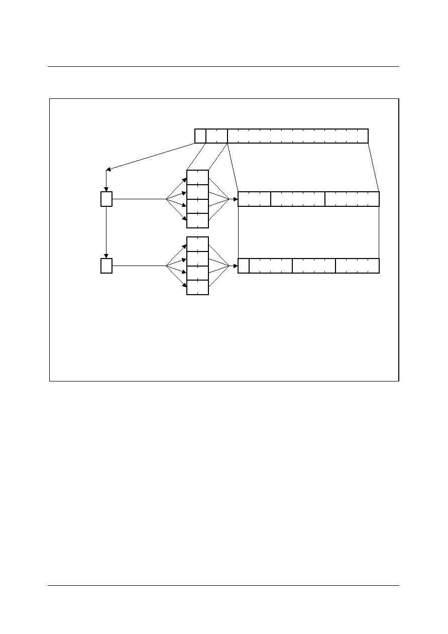
SDA 6000 / SDA 6001
PRELIMINARY DATA SHEET
Version 3.00
Display Generator
10 - 18
Micronas
Figure 10-12 16-bit Pixel Format (4:4:4:2/TTX) for Use in Frame Buffer
Pixels in 16-bit format which are stored in TTX format contain two 5-bit colour look up
vectors and two flash mode indicator bits. The flash mode indicator bits are used to
choose the flash rate and the flash phase. The meaning of flash is: The colour alternates
between two 5-bit colour vectors (FlashC and Pixel) which are chosen within the format
definition.
� Non Flash: Flash can be disabled if both 5-bit colour vectors point to the same CLUT2
location.
� Inverted Flash: Inverted flash is supported by exchanging the `FlashC' vector with the
`Pixel' vector.
UED11181
M TR(1..0)
Pixel(12..0)
FlashC(4..0)
3)
Pixel(4..0)
4)
(2..0)
C
2)
Blue(3..0)
Green(3..0)
5)
5)
Red(3..0)
5)
I
1)
1
1
1
0
0
0
1
0
0
1
1
1
1
0
0
0
2 Hz Flash, Phase 3
2 Hz Flash, Phase 2
2 Hz Flash, Phase 1
1 Hz Flash
0
Transparency Level 1
Transparency Level 2
Transparency Level 3
Transparency Level 4
1
Format
16-Bit TTX
Format
16-Bit 4:4:4:2
1)
I - Italic Subpixel
C - CLUT2 Selector in TTX mode
2)
FlashC - CLUT2 Vector for Flash Colour in TTX mode
3)
Pixel - CLUT2 Vector for Pixel in TTX mode
4)
Red Green Blue - Pixel RGB Colour in 4:4:4:2 mode
5)

SDA 6000 / SDA 6001
PRELIMINARY DATA SHEET
Version 3.00
Display Generator
10 - 19
Micronas
Figure 10-13 Internally Generated Flash Signals in Different Flash Phases
5-bit colour look up vectors are converted into a 12-bit RGB value and a 2-bit
transparency level by CLUT2 during display. To do this, the input side of CLUT2 the 5-
bit look up value is used for Bit0 to Bit4, the C
2
-values are used as Bit7 to Bit5. The 12-
bit RGB value is fed to the D/A converter and the 2-bit transparency information to the
BLANK/COR pins.
16-bit format pixels which are stored in the 12-bit RGB format are not passing the
CLUT2. The 12-bit RGB value and the 2-bit transparency information is directly fed into
the D/A converter and the BLANK/COR pins.
Frame Buffer in 16-bit Pixel Format (5:6:5)
In this mode the frame buffer contains RGB values with 5 bits for red colour components,
6 bits for green colour components and 5 bits for blue colour components:
Figure 10-14 16-bit Pixel Format (5:6:5) for Use in Frame Buffer
Transparency between layers is not supported if this mode is in use. The 5:6:5 format is
directly transferred to the D/A converter. CLUT2 is out of use in this mode.
UED11182
Fast Rate Flash. Phase 3. Normal Flash
Fast Rate Flash. Phase 2. Normal Flash
Fast Rate Flash. Phase 1. Normal Flash
Slow Rate Flash. Normal Flash
UED11183
Blue
Green
Red
Green
4
3
2
1
0
5
4
3
2
1
0
4
3
2
1
0
15 14
11
13 12
10
9
7
8
6
4
5
3
0
2
1
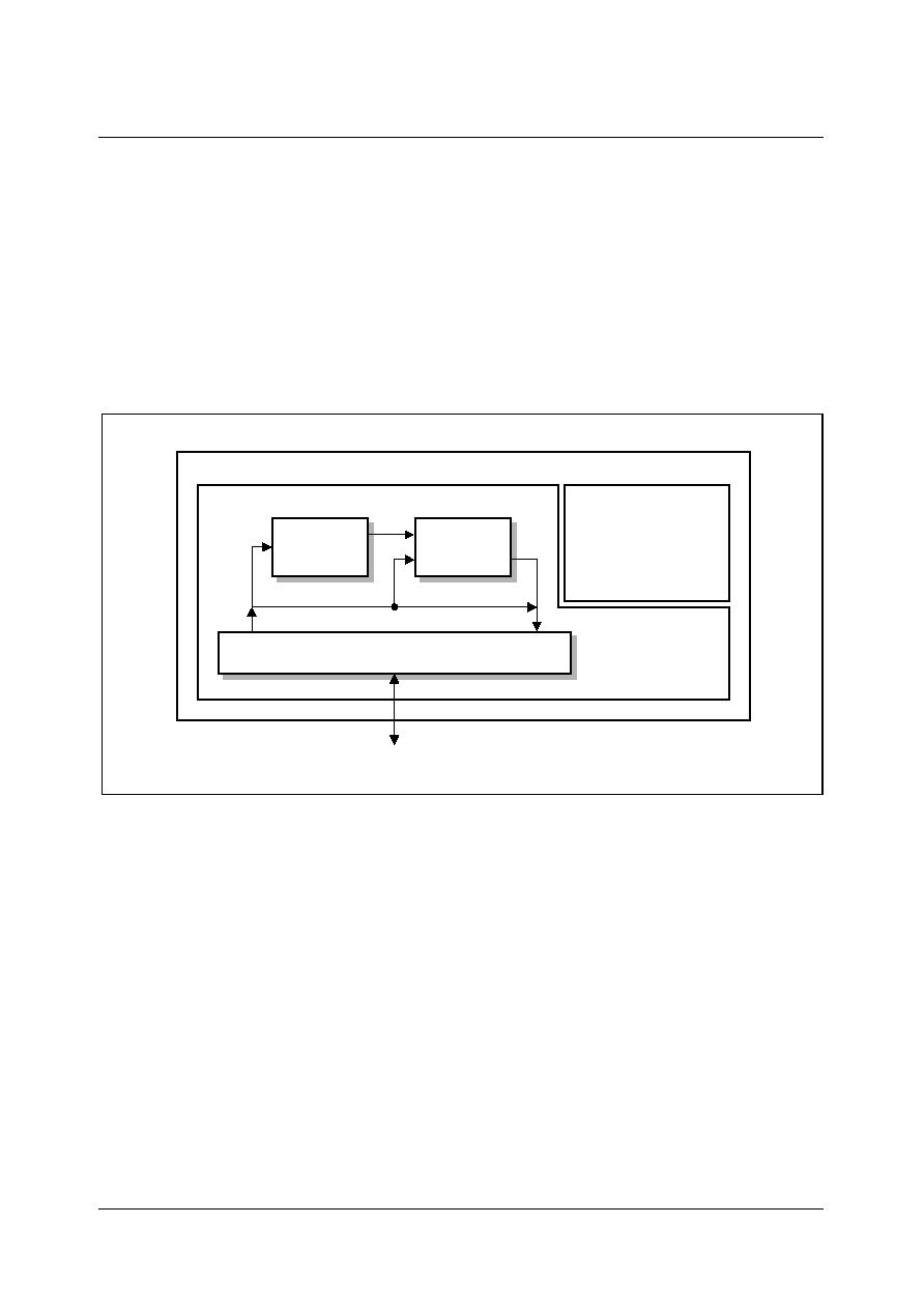
SDA 6000 / SDA 6001
PRELIMINARY DATA SHEET
Version 3.00
Display Generator
10 - 20
Micronas
10.5
Initialization of Memory Transfers
Transferring an input format of the source area to an output format in the destination area
is supported by different transfer modes. For this, a pixel modification unit and CLUT1 of
the GA is used. CLUT1 has a size of 256
�
16 bit.
Next to the transfer mode the transfer areas (source and destination) must be defined by
GA instructions. Source is either an address in the external memory or a constant value
coming from CLUT1. Destination is always an address in the external memory. Constant
values coming from CLUT1 are used to draw lines or fill parallelograms.
Figure 10-15 Overview of GA
10.5.1
Transfer Modes
Different transfer modes are available. The table below shows all possible combinations
of input and output formats.
`Transparency available' means that if transparency mode is chosen (see also GAI-
instruction `TAR' (Bit: TRM)) and Bit TR1 of the output word is set to `0' (refer also to
Figure 10-12) this pixel is written to the destination, otherwise this pixel is not written to
the destination.
`Modification' describes in which way the output information is generated by using the
input information, CLUT1 and the settings of the `TAR'-instruction. Using 16-bit TTX
output two bits are replaced by another 2 bits (Flash) which are also defined by graphic
accelerator instruction `TAR'. The table below shows all possible combinations of input
and output formats:
Display Generator Interface (DGI)
UED11184
Memory
GA
DG
(256 x 16)
Pixel
Modification
CLUT1
SRU

SDA 6000 / SDA 6001
PRELIMINARY DATA SHEET
Version 3.00
Display Generator
10 - 21
Micronas
Table 10-5
Supported Transfer Modes
TMOD
(4 ... 0)
Input
Format
Output
Format
Transparency
Available
Modification
00000
1-bit
bitmap
16-bit
(TTX)
No
OUT(15) = `0'
OUT(14 ... 13) = FLA(1 ... 0)
OUT(12 ... 0) = CLUT1(`0000000' &
IN(0))(12 ... 0)
00001
1-bit
bitmap
16-bit
(4:4:4:2)
Yes
OUT(15) = `1'
OUT(14 ... 13) = CLUT1(`0000000' &
IN(0))(14 ... 13))
OUT(12) = IT
OUT(11 ... 0) = CLUT1(`0000000' &
IN(0))(11 ... 0))
00010
1-bit
bitmap
8-bit
No
OUT(7 ... 0) = CLUT1(`0000000' &
IN(0))(7 ... 0)
00011
1-bit
bitmap
16-bit
(5:6:5)
No
OUT(15 ... 0) = CLUT1(`0000000' &
IN(1 ... 0))(15 ... 0))
00100
2-bit
bitmap
16-bit
(TTX)
No
OUT(15) = `0'
OUT(14 ... 13) = FLA(1 ... 0)
OUT(12 ... 0) = CLUT1(`000000' &
IN(1 ... 0))(12 ... 0)
00101
2-bit
bitmap
16-bit
(4:4:4:2)
Yes
OUT(15) = `1'
OUT(14 ... 13) = CLUT1(`0000000' &
IN(1 ... 0))(14 ... 13))
OUT(12) = IT
OUT(11 ... 0) = CLUT1(`0000000' &
IN(1 ... 0))(11 ... 0))
00110
2-bit
bitmap
8-bit
No
OUT(7 ... 0) = CLUT1(`000000' &
IN(1 ... 0))(7 ... 0)
00111
2-bit
bitmap
16-bit
(5:6:5)
No
OUT(15 ... 0) = CLUT1(`000000' &
IN(1 ... 0))(15 ... 0))
01000
4-bit
bitmap
16-bit
(TTX)
No
OUT(15) = `0'
OUT(14 ... 13) = FLA(1 ... 0)
OUT(12 ... 0) = CLUT1(`0000' &
IN(3 ... 0))(12 ... 0)

SDA 6000 / SDA 6001
PRELIMINARY DATA SHEET
Version 3.00
Display Generator
10 - 22
Micronas
01001
4-bit
bitmap
16-bit
(4:4:4:2)
Yes
OUT(15) = `1'
OUT(14 ... 13) = CLUT1(`0000000' &
IN(3 ... 0))(14 ... 13))
OUT(12) = IT
OUT(11 ... 0) = CLUT1(`0000000' &
IN(3 ... 0))(11 ... 0))
01010
4-bit
bitmap
8-bit
No
OUT(7 ... 0) = CLUT1(`0000' &
IN(3 ... 0))(7 ... 0)
01011
4-bit
bitmap
16-bit
(5:6:5)
No
OUT(15 ... 0) = CLUT1(`0000' &
IN(3 ... 0))(15 ... 0))
01100
8-bit
bitmap
16-bit
(TTX)
No
OUT(15) = `0'
OUT(14 ... 13) = FLA(1 ... 0)
OUT(12 ... 0) =
CLUT1(IN(7 ... 0))(12 ... 0)
01101
8-bit
bitmap
16-bit
(4:4:4:2)
Yes
OUT(15) = `1'
OUT(14 ... 13) = CLUT1(`0000000' &
IN(7 ... 0))(14 ... 13))
OUT(12) = IT
OUT(11 ... 0) = CLUT1(`0000000' &
IN(7 ... 0))(11 ... 0))
01110
8-bit
bitmap
8-bit
No
OUT(7 ... 0) =
CLUT1(IN(7 ... 0))(7 ... 0)
01111
8-bit
bitmap
16-bit
(5:6:5)
No
OUT(15 ... 0) =
CLUT1(IN(7 ... 0))(15 ... 0))
10000
CLUT1
input
8-bit
No
OUT(7 ... 0) = CLUT1(0)(7 ... 0)
10001
CLUT1
input
16-bit
(TTX)
No
OUT(15) = `0'
OUT(14 ... 13) = FLA(1 ... 0)
OUT(12 ... 0) = CLUT1(0)(12 ... 0)
10010
CLUT1
input
16-bit
(4:4:4:2)
Yes
OUT(15) = `1'
OUT(14 ... 0) = CLUT1(0)(14 ... 0))
10011
16-bit
(TTX or
4:4:4:2)
16-bit
(TTX or
4:4:4:2)
Only In 4:4:4:2
Mode
OUT(15 ... 0) = IN(15 ... 0)
Table 10-5
Supported Transfer Modes (cont'd)
TMOD
(4 ... 0)
Input
Format
Output
Format
Transparency
Available
Modification

SDA 6000 / SDA 6001
PRELIMINARY DATA SHEET
Version 3.00
Display Generator
10 - 23
Micronas
Note: There is no transfer mode defined which uses the 2-bit format as an output format,
because in this case layer 2 is restricted to a width of 64 pixels. If the 2-bit format
is required, the direct byte by byte transfer can be used.
10.5.2
Transfer Areas
Next to the transfer mode the transfer area has to be defined by graphic accelerator
instructions (GAI). For source and destination, `linear' and `rectangle' areas can be
defined.
`Linear' means that data is accessed byte by byte without any irregularity in the
addressing of the memory.
`Rectangle' means that after the access of n bytes defined by a parameter `width' an
`offset' to the last address is automatically added. This feature can be used if an array of
data has to be copied from one memory location into another (bigger) array at any other
memory location. The linear addressing is a subset of the rectangle addressing scheme
if `offset' is set to `0'.
Source Area
There are different settings necessary to define the source area. These settings are
done by using the graphic accelerator instruction set. The table below describes the
necessary settings and corresponding GAIs with the affected bit position inside the GAI:
10100
8-bit
data
8-bit data No
OUT(7 ... 0) = IN(7 ... 0)
Others
Reserved
Used GAI
Bit Position Inside
GAI
Description
SDR
S_ADDR
Start address of source area
TSR
WIDTH_IN
Width of source area
TOR
S_OFFSET
Offset to describe rectangular source
areas
Table 10-5
Supported Transfer Modes (cont'd)
TMOD
(4 ... 0)
Input
Format
Output
Format
Transparency
Available
Modification

SDA 6000 / SDA 6001
PRELIMINARY DATA SHEET
Version 3.00
Display Generator
10 - 24
Micronas
As described before, there are seven different formats on the input side of the transfer:
� 1-bit bitmap
� 2-bit bitmap
� 4-bit bitmap
� 8-bit bitmap
� 8-bit data (used for direct data transfer)
� CLUT1 input (used for drawing of filled parallelograms, rectangles, lines)
� 16-bit (4:4:4:2) RGB
CLUT1 input does not need any more detailed area description. The input value comes
directly from the address `0' of CLUT1 and not from the RAM. This mode can be used
for drawing lines, filling rectangles or parallelograms. For the other input modes a more
detailed description is given below:
From the point of view of the register settings, which are used to define the source area,
the different input formats can be divided in three groups which are handled in different
ways.
Group 1:
Group 2:
Group3:
1-bit bitmap8-bit data16-bit pixel format (4:4:4:2)
2-bit bitmap8-bit bitmap
4-bit bitmap
Formats of group 1 are formats which define each pixel with less than a byte. Group 2
formats are formats which define each pixel by 8 bits, and group 3 formats are formats
which define each pixel by 16 bits.
Group 1:
In 1-bit bitmap, 2-bit bitmap and 4-bit bitmap input mode it is expected, that the bitmaps
are stored linearly in the memory as described in Chapter 10.4.1. Therefore the settings
of WIDTH_IN as well as S_OFFSET are ignored. Only the 24-bit source address pointer
S_ADDR is used. The amount of pixels which are read from the source and written to
the destination is only defined by the destination settings. The user has to take care that
the destination settings fit with the bitmap inherent alignments.
Group 2:
In this mode WIDTH_IN and S_OFFSET are also taken into account. The amount of
memory which is described by WIDTH_IN and S_OFFSET is described by numbers of
bytes.
Group 3:
In this mode WIDTH_IN and S_OFFSET are also taken into account. The amount of
memory which is described by WIDTH_IN and S_OFFSET is described by numbers of
words.
Note: The number of bytes to be read from the source area is defined by the destination
area (see below) and the transfer mode. This is why no explicit definition of height
is needed for the source.
SDA 6000 / SDA 6001
PRELIMINARY DATA SHEET
Version 3.00
Display Generator
10 - 25
Micronas
Figure 10-16 Use of Register Settings to Specify Source Area
Destination Area
There are additional settings necessary to define the destination area. The table below
describes the settings and the corresponding GAIs with the affected bit position inside
the GAI:
Next to the destination area itself a clipping area can be defined. The clipping area needs
to be defined within the destination area. During a memory transfer these `clipped'
memory areas are excluded from the transfer. The table below describes the settings
and the corresponding GAIs with the affected bit positions inside the GAI:
Used GAI
Bit Position Inside GAI
Description
DDR
D_ADDR
Start address of destination area
TDR
HEIGHT_OUT,
WIDTH_OUT
Height and width of destination
area
TOR
D_OFFSET
Offset to describe rectangular
destination areas
Used GAI
Bit Position Inside GAI
Description
CUR
C_ADDR
Start address of clipping area
CBR
HEIGHT_CLIP,
WIDTH_CLIP
Height and width of clipping area
CBR, CUR
C_OFFSET
Offset to describe rectangular
clipping areas
UED11185
S_ADDR
S_OFFSET (TOR)
MEMORY
WIDTH_IN (TSR)
Source Area

SDA 6000 / SDA 6001
PRELIMINARY DATA SHEET
Version 3.00
Display Generator
10 - 26
Micronas
As described before, there are five different formats on the output side of the transfer:
(Also please refer to Chapter 10.4.2)
� 8-bit format CLUT2 vector
� 16-bit format (4:4:4:2) RGB
� 16-bit format (TTX) CLUT2 vector
� 16-bit format (5:6:5) RGB
� Direct data transfer (byte by byte)
From the point of view of the register settings which are used to define the alignment of
the destination area, these formats can be divided in two groups. Each group is handled
in a different way.
Group 1:
Group 2:
16-bit format (4:4:4:2) RGB
8-bit format CLUT2 vector
16-bit format (TTX) CLUT2 vector
8-bit data (byte by byte transfer)
16-bit format (5:6:5) RGB
Formats of group 1 are formats which define each pixel by 16 bits. Group 2 formats are
formats which define each pixel by 8 bits.
Note: Bit fields HEIGHT_CLIP, HEIGHT_OUT and WIDTH_CLIP, WIDTH_OUT
describe the height and width of the destination in count of pixels and not in bytes.
So for output formats of group 1 the memory area which is described by a
HEIGHT_OUT value and a WIDTH_OUT value needs the double amount of
memory, than output formats which are described by the same HEIGHT_OUT
value and WIDTH_OUT value for output formats of group 2. Also, the OFFSET
values are pixels and not bytes or words.
C_ADDR and D_ADDR are real byte addresses in memory.
Note: For a rectangle destination area the sum of WIDTH and D_OFFSET of the
destination area must be equal to the width of the frame buffer (WIDTH_L1(2)).
Otherwise the shape of the copied frame will be a parallelogram and not a
rectangle.
Note: For a rectangle clipping area inside the destination area the sum of the clipping
offset and the clipping width must be the same as the sum of the destination area
width and the destination offset. Otherwise the clipping area will be a
parallelogram and not a rectangle.
Note: Source area and destination area should not overlap. Otherwise it may appear
that a pixel is overwritten as a destination pixel, and afterwards used as a source
pixel.
SDA 6000 / SDA 6001
PRELIMINARY DATA SHEET
Version 3.00
Display Generator
10 - 27
Micronas
Meaning of Double Width and Double Height during Transfer
The destination area can be stretched horizontally and vertically by using GA instruction
TAR.
If double width (TDW) is set to `1', the graphic accelerator writes each pixel twice
horizontally to the destination area.
If double height (TDH) is set to `1' in the destination output side each pixel in vertical
direction is repeated twice.
For example: If double width is set to `1' and quadruple height is set to `1' each pixel of
the source area needs 8 pixels of the destination area.
Note: Parameters like WIDTH_OUT, WIDTH_CLIP, HEIGHT_OUT and HEIGHT_CLIP
are still pixel related. WIDTH_OUT, HEIGHT_OUT and D_OFFSET have to be
adapted by the software to get a complete character. Clipping is not affected by
TDH and TDW.
The following table is an example of a 1-bit bitmap (30
�
50) which should be transferred
either in normal size or in double size to an 8 bit output format in a frame buffer with a
size of 100
�
200 pixels.
Note: In case of double width transfer WIDTH_OUT has to be an even number. In case
of double/quad height transfer HEIGHT_OUT has to be an even/divisable by 4
number.
TQH
TDH
Meaning
0
0
Normal transfer
0
1
If double height (TDH) is set to `1' and quadruple height (TQH) is set
to `0' in the destination output side each pixel in vertical direction is
repeated twice.
1
X
If quadruple height (TQH) is set to `1' on the destination output side
each pixel in vertical direction is repeated four times.
Parameters
TDW = 0; TDH = 0; TQH = 0
TDW = 1; TDH = 1; TQH = 0
WIDTH_L1
100
HEIGHT_L1
200
WIDTH_IN
30
WIDTH_OUT
30
60
D_OFFSET
70
40
HEIGHT_OUT
50
100
SDA 6000 / SDA 6001
PRELIMINARY DATA SHEET
Version 3.00
Display Generator
10 - 28
Micronas
Figure 10-17 gives a graphical overview of how to specify the different areas.
Figure 10-17 Use of Register Settings to Specify Destination and Clipping Area
10.5.3
Italic Mode
For transfer modes with 16-bit (4:4:4:2) format as an output, an automatic italic transfer
option is available. If italic mode is chosen only the destination area (not the source area)
is affected. The following two figures explain the different representation of pixels in the
frame buffer in non-italic and italic mode.
Figure 10-18 Result for a Non-italic Transferred Memory Area in Frame Buffer
UED11186
D_ADDR
D_OFFSET (TOR)
Frame Buffer
WIDTH_OUT (TDR)
Destination Area
WIDTH_L1(2) (FSR)
HEIGHT_OUT (TDR)
C_ADDR
FB_ADDR
HEIGHT_CLIP (CBR)
WIDTH_CLIP (CBR)
C_OFFSET (CUR, CBR)
C_OFFSET (CUR, CBR)
HEIGHT_L1(2) (FSR)
Clipping Area
UED11187
HEIGHT_OUT
D_ADDR
D_OFFSET
WIDTH_OUT
D_OFFSET
0
0
0
0
0
0
0
0
0
0
Bit 'I' of
4:4:4:2 format
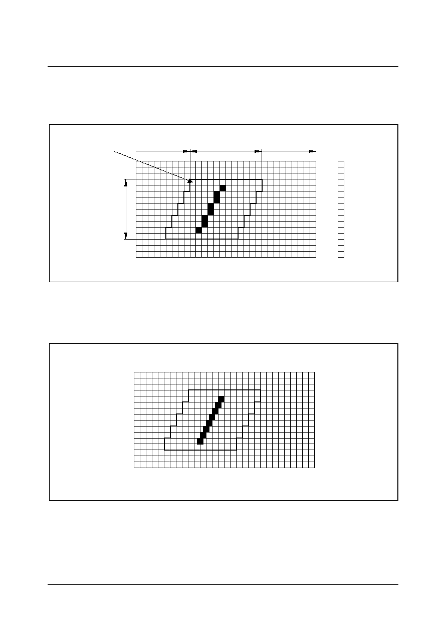
SDA 6000 / SDA 6001
PRELIMINARY DATA SHEET
Version 3.00
Display Generator
10 - 29
Micronas
If this transfer is executed with the same register settings but in italic mode instead of
non italic mode, the subsequent destination area is used inside the frame buffer:
Figure 10-19 Result for a Italic Transferred Memory Area in Frame Buffer
Next to the destination pixel offset from line to line, the italic bit (`I') alternates from line
to line. This italic bit is used to control the D/A converter to realize a horizontal line
alternating half pixel shift on RGB output.
Figure 10-20 Result for an Italic Transferred Memory Area at D/A Converter Output
Note: Italic can not be used together with double width and double/quad height transfers.
UED11188
HEIGHT_OUT
D_ADDR
D_OFFSET
WIDTH_OUT
D_OFFSET
0
1
0
1
0
1
0
1
0
1
Bit 'I' of
4:4:4:2 format
UED11189

SDA 6000 / SDA 6001
PRELIMINARY DATA SHEET
Version 3.00
Display Generator
10 - 30
Micronas
10.6
Register Description
10.6.1
Special Function Registers
The display generator is controlled by 3 special function registers and a list of accelerator
instructions. Two of the registers define the position and the length of the instruction list,
and one register is used for general control of the DG. After the list of instructions (GAIs)
is written to the memory, the start address and the length of this list must be written to
special function registers GPRGCRH and GPRGCRL. Then the controller commands
the GA to execute these instructions (see SFR DGCON). After the GA has finished
executing all GAIs, the GA gives the controller an interrupt (GAFIR).
Note: GPRGCRH, GPRGCRL and DGCON are the only special function registers to
control the display generator. GAIs described in the next paragraph are stored in
the RAM and not defined after power on.
GPRGCRH
Reset Value: 0000
H
GPRGCRL Reset
Value:
0000
H
DGCON is for general control of the DG.
Bit
Function
GCR
(8 ... 0)
Defines the amount of GAIs in the instruction list.
GCR
�
4 is the length of the GAI area in count of bytes.
Note: After the last instruction is executed an interrupt is given to the
controller
GPR
(23 ... 17)
Define the MSBs of the 23-bit address pointer to the start of the GAI
area.
Bit
Function
GPR
(16 ... 1)
Define the LSBs of the 23-bit address pointer to the start of the GAI
area.
5
4
3
2
1
0
11
10
9
8
7
6
15
14
13
12
rw
rw
GCR (8..0)
GPR (23..17)
5
4
3
2
1
0
11
10
9
8
7
6
15
14
13
12
rw
GPR (16..1)

SDA 6000 / SDA 6001
PRELIMINARY DATA SHEET
Version 3.00
Display Generator
10 - 31
Micronas
DGCON
Reset Value: 0000
H
Bit
Function
EADG
Enables access from DG to SDRAM.
0:
All requests from DG (SRU and GA) to the memory are disabled.
1:
The DG has normal access to the memory.
Note: The running memory access is finalized before this bit becomes
active.
EODG
Enables output of DG.
0:
All outputs of the DG are disabled (RGB outputs are switched to
black level, COR = 0 and BLANK = 1) (`Normal' pin polarity
assumed. Please refer also to register SCR).
1:
The outputs have the function according to the specifications
described in the following paragraphs.
Note: The SRU registers FBR and DBR have to be programmed with a
valid memory address before enabling display output.
STGA
Starts processing of the instruction list by the GA
0:
STGA has to be reset by SW before the GA can be started again.
1:
The GA starts the execution of the instruction list at address GPR.
It ends after the specified number of instructions (see bit field
GCR) is executed. After that an interrupt (GAFIR) is given to the
controller.
BSYGA
0:
GA is idle, waiting for GAI sequence.
1:
GA is busy, GAI sequence is processed.
5
4
3
2
1
0
11
10
9
8
7
6
15
14
13
12
rw
rw
-
-
-
-
-
-
-
-
-
-
-
-
BSY
GA
ST
GA
EO
DG
EA
DG
rw
r

SDA 6000 / SDA 6001
PRELIMINARY DATA SHEET
Version 3.00
Display Generator
10 - 32
Micronas
The register PXDEL controls an individual delay of 0 ... 2 clock cycles of the SRU
outputs. Each output (R, G, B, Italic, blank, cor) is contolled by 2 bits in the PXDEL
register.
PXDEL
Reset Value: 0000
H
Bits set to
"00" - no delay
"01" - delay of 1 pixel clock cycle
"10" - delay of 2 pixel clock cycles
"11" - reserved
The reset value of PXDEL is set to 0000
H
, which means no dely of the SRU outputs after
reset.
Bits
1 ... 0
delay for red
3 ... 2
delay for green
5 ... 4
delay for blue
7 ... 6
delay for italic
9 ... 8
delay for blank
11 ... 10
delay for cor
15 ... 12
reserved
5
4
3
2
1
0
11
10
9
8
7
6
15
14
13
12
res
res
res
res
Tcor
Tblank
Titalic
Tblu
Tgreen
Tred
w
w
w
w
w
w
w
w
w
w
w
w
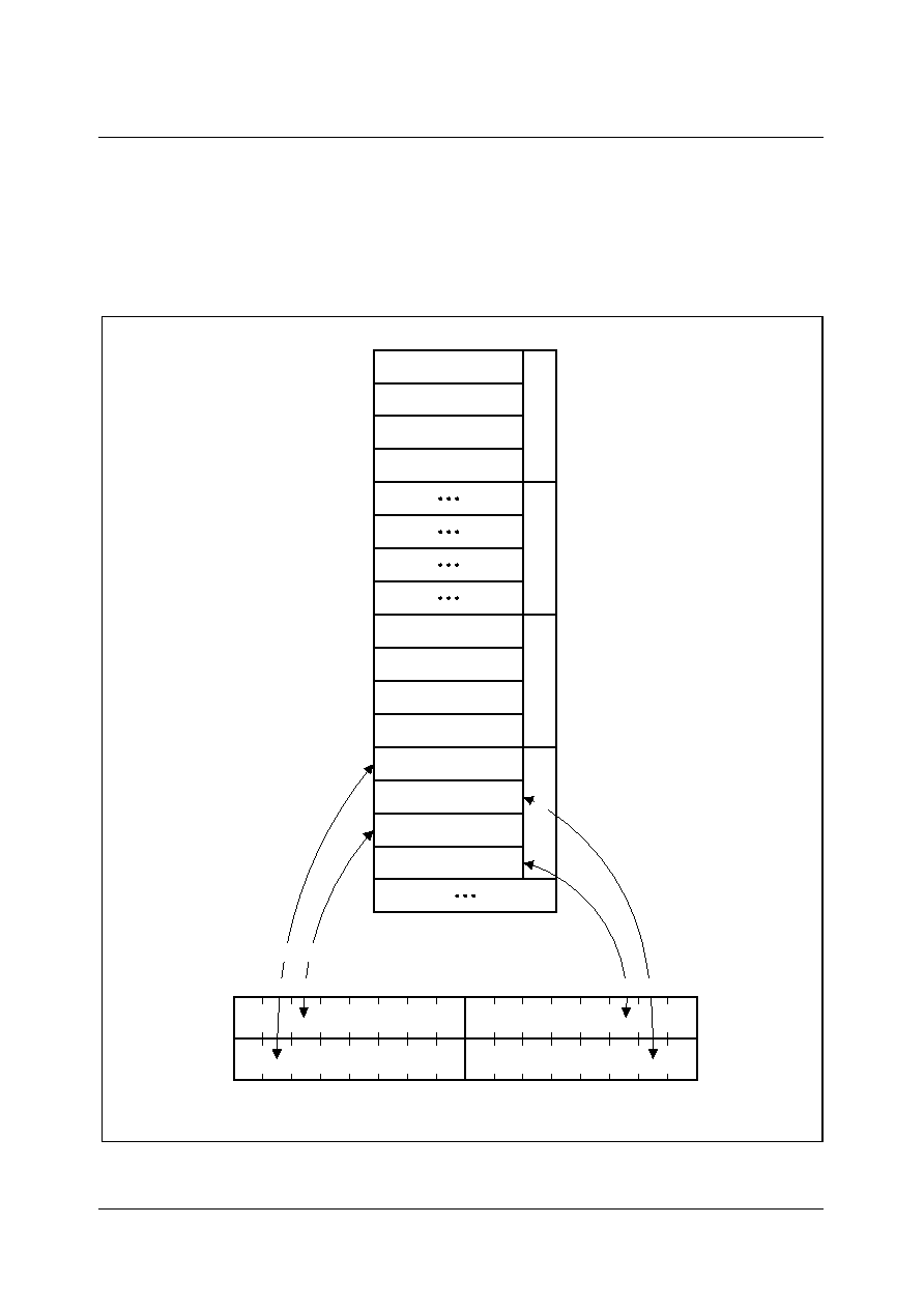
SDA 6000 / SDA 6001
PRELIMINARY DATA SHEET
Version 3.00
Display Generator
10 - 33
Micronas
10.7
Description of Graphic Accelerator Instructions
GAIs are 32-bit instructions which are used as an interface from
�
C to DG. They are
written sequentially to the SDRAM by the controller in form of an instruction list.
Figure 10-21 shows the organization of GAIs in the memory.
Figure 10-21 Organization of GAIs in the External SDRAM
UED11190
Byte Address n+3+k
Byte Address n+2+k
Byte Address n+1+k
Byte Address n+k
GAI-No. k
GAI-No. ...
GAI-No. 1
Byte Address n+4
Byte Address n+5
Byte Address n+6
Byte Address n+7
GAI-No. 0
Byte Address n
Byte Address n+1
Byte Address n+2
Byte Address n+3
24
8
9
25
10
26
11
27
12
28
13
29
14
30
15
31
GAI_BYTE 1
GAI_BYTE 3
GAI_BYTE 2
GAI_BYTE 0
6
22
7
23
5
4
21 20
3
2
19
18
1
0
16
17
Standard Format for GAIs:
x
4
4
x
4
x
4
x
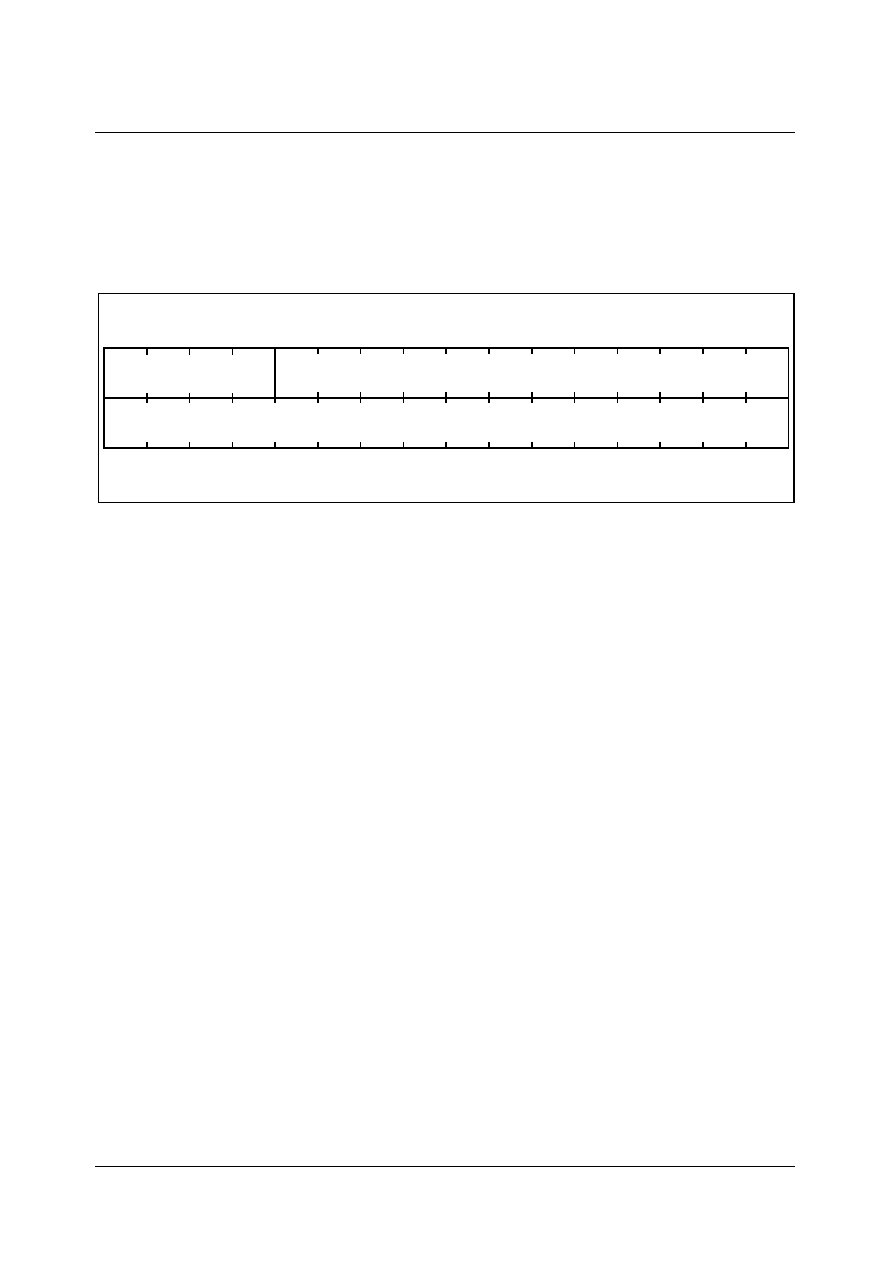
SDA 6000 / SDA 6001
PRELIMINARY DATA SHEET
Version 3.00
Display Generator
10 - 34
Micronas
In the following GAI description, `�' means that these bits are reserved for future use and
have to be set to `0'. The meaning of an instruction is not given by the physical location
(address) of the instruction but by its opcode which is represented by bits 31 ... 28. Bits
27 ... 0 are equivalent to an operand.
Figure 10-22 GAI Instruction Format
There are two types of GAIs. One type is used to setup global parameters for SRU and
GA, like SRU setup, frame buffer setup or CLUT setup. The second type of GAI is used
to setup the transfer parameters for DMA functions.
Global Parameters
The following global instructions are only executed by the GA during the vertical sync
area. If such a GA-instruction is read by the GA outside the V-sync area, it waits until the
next V-sync appears.
Note: The V-sync area is defined for that purpose as the first 4 lines of a field.
� SRU setup
SAR (opcode = 1111) - set screen attributes
� Frame buffer 1 (layer 1) and frame buffer 2 (layer 2) setup
FBR (opcode = 1000) - set address of the beginning of frame buffer 1
FSR (opcode = 1001) - set size of frame buffer 1
DBR (opcode = 1010) - set address of the beginning of frame buffer 2
DSR (opcode = 1011) - set size of frame buffer 2
DCR (opcode = 1100) - set frame buffer 2 reference coordinates
� CLUT Setup
CLR (opcode = 1101) - set contents of the CLUT1 or CLUT2
Note: If CLUT2 should be loaded the GA waits until the next V-sync appears.
� No operation
NOP (opcode = 1110) - no operation
31
30
29
28
27
26
25
24
23
22
21
20
19
18
17
16
15
14
13
12
11
10
9
8
7
6
5
4
3
2
1
0
Operand(s)
Operand(s)
Opcode
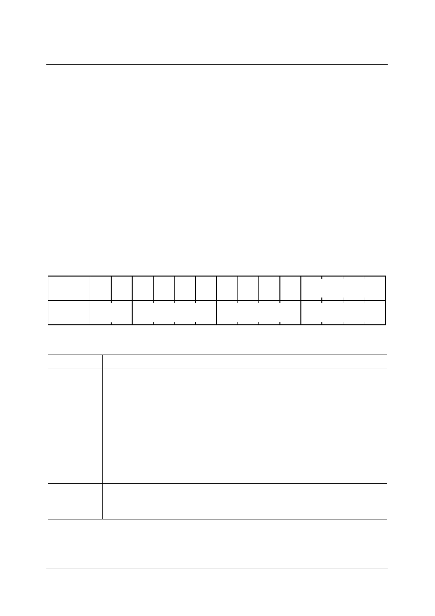
SDA 6000 / SDA 6001
PRELIMINARY DATA SHEET
Version 3.00
Display Generator
10 - 35
Micronas
Transfer Parameters
These instructions are immediately executed by the GA.
� CUR (opcode = 0000) - set clipping coordinates
� CBR (opcode = 0001) - set clipping coordinates
� SDR (opcode = 0010) - set source descriptor for data transfer
� DDR (opcode = 0011) - set destination descriptor for data transfer
� TSR (opcode = 0100) - set definitions for source memory area
� TDR (opcode = 0101) - set definitions for destination memory area
� TOR (opcode = 0110) - set offset definitions for transferred area
� TAR (opcode = 0111) - set attributes for transfer
10.7.1
Screen Attributes (SAR)
This instruction controls different screen attributes.
SAR
Bit
Function
SBTL
Screen Background Transparency under Layer Area
Defines whether the screen background area is transparent under a
layer 1 (2) area or not.
0:
The screen background within a layer area is not transparent.
Under transparent layer pixels the background colour can be seen.
1:
The screen background within a layer area is transparent. Under
transparent layer pixels the video can be seen.
Note: Transparency definitions for the screen background outside a
layer area are made with bits STR. Also please refer to
Chapter 10.3.3.
DMODE
(3 ... 0)
Display Mode Bits
Defines the possible combinations of both layers with the available pixel
formats. Please see table `Display Modes' below.
31
30
29
28
27
26
25
24
23
22
21
20
19
18
17
16
15
14
13
12
11
10
9
8
7
6
5
4
3
2
1
0
STR(1..0)
GREEN(3..0)
BLUE(3..0)
DDW
DDH
RED(3..0)
1
-
-
-
-
-
-
SB
TL
DMODE(3..0)
1
1
1
-

SDA 6000 / SDA 6001
PRELIMINARY DATA SHEET
Version 3.00
Display Generator
10 - 36
Micronas
DDW
Double Width Display
0: Normal
width
1:
Double width. The contents of the screen are stretched in
horizontal direction. The SRU repeats the same pixel information
twice in horizontal direction.
Note: DDW = `1' the frame buffer width (WIDTH_L1(L2) has to be
divided by two to get the same area displayed on the screen.
DDH
Double Height Display
0: Normal
height
1:
Double height. The contents of the screen are stretched in vertical
direction. The SRU repeats the same pixel information twice in
vertical direction.
Note: DDH = `1' the frame buffer height (HEIGHT_L1(L2) has to be
divided by two to get the same area displayed on the screen.
STR
(1 ... 0)
Screen Background Transparency Level
Define the transparency of the screen background area outside the layer
area. Please refer to Chapter 10.3.3.
RED
(3 ... 0)
Screen Background Red Colour
4-bit red component
GREEN
(3 ... 0)
Screen Background Green Colour
4-bit green component
BLUE
(3 ... 0)
Screen Background Blue Colour
4-bit blue component
Bit
Function

SDA 6000 / SDA 6001
PRELIMINARY DATA SHEET
Version 3.00
Display Generator
10 - 37
Micronas
Table 10-6
Display Modes
DMODE
(3 ... 0)
Layer Formats
Layer Mode
Layer 1
Layer 2
0000
16-bit (4:4:4:2 or TTX)
�
Layer 2 switched off
0001
8-bit
�
Layer 2 switched off
0010
16-bit (5:6:5)
�
Layer 2 switched off
0011
�
�
Layer 1 & 2 switched off
0100
reserved
�
�
0101
reserved
0110
16-bit (4:4:4:2 or TTX)
2-bit
overlapped
0111
reserved
1000
16-bit (4:4:4:2 or TTX)
16-bit (4:4:4:2 or TTX)
embedded
1001
8-bit
8-bit
embedded
1010
16-bit (4:4:4:2 or TTX)
8-bit
embedded
1011
8-bit
16-bit (4:4:4:2 or TTX)
embedded
1100
16-bit (5:6:5)
16-bit (5:6:5)
embedded
1101
reserved
1110
1111

SDA 6000 / SDA 6001
PRELIMINARY DATA SHEET
Version 3.00
Display Generator
10 - 38
Micronas
10.7.2
Startaddress of Layer 1 (FBR)
The start address of frame buffer 1 in the memory must be set by the controller.
FBR
10.7.3
Size of Layer 1 (FSR)
FSR
Bit
Function
FB_ADDR
(23 ... 0)
Startaddress of frame buffer 1
Bit 23 ... 0 of a byte address.
Bit
Function
HEIGHT_L1
(9 ... 0)
Height of Frame Buffer 1
The height of the frame buffer can vary between 0 (HEIGHT_L1 = `0'
d
)
and 1023 pixels (HEIGHT_L1 = `1023'
d
).
WIDTH_L1
(10 ... 0)
Width of Frame Buffer 1
The width of the frame buffer can vary between 0 (WIDTH_L1 = `0'
d
) and
2046 pixels (WIDTH_L1 = `2046'
d
).
31
30
29 28
27
26
25
24
23
22
21
20
19
18
17
16
15
14
13
12
11
10
9
8
7
6
5
4
3
2
1
0
FB_ADDR(15..0)
0
-
-
-
FB_ADDR(23..16)
1
0
0
-
31
30
29
28
27 26
25
24
23
22
21
20
19
18
17
16
15
14
13
12
11
10
9
8
7
6
5
4
3
2
1
0
-
WIDTH_L1(10..0)
-
-
-
-
0
-
HEIGHT_L1(9..0)
1
0
1
-
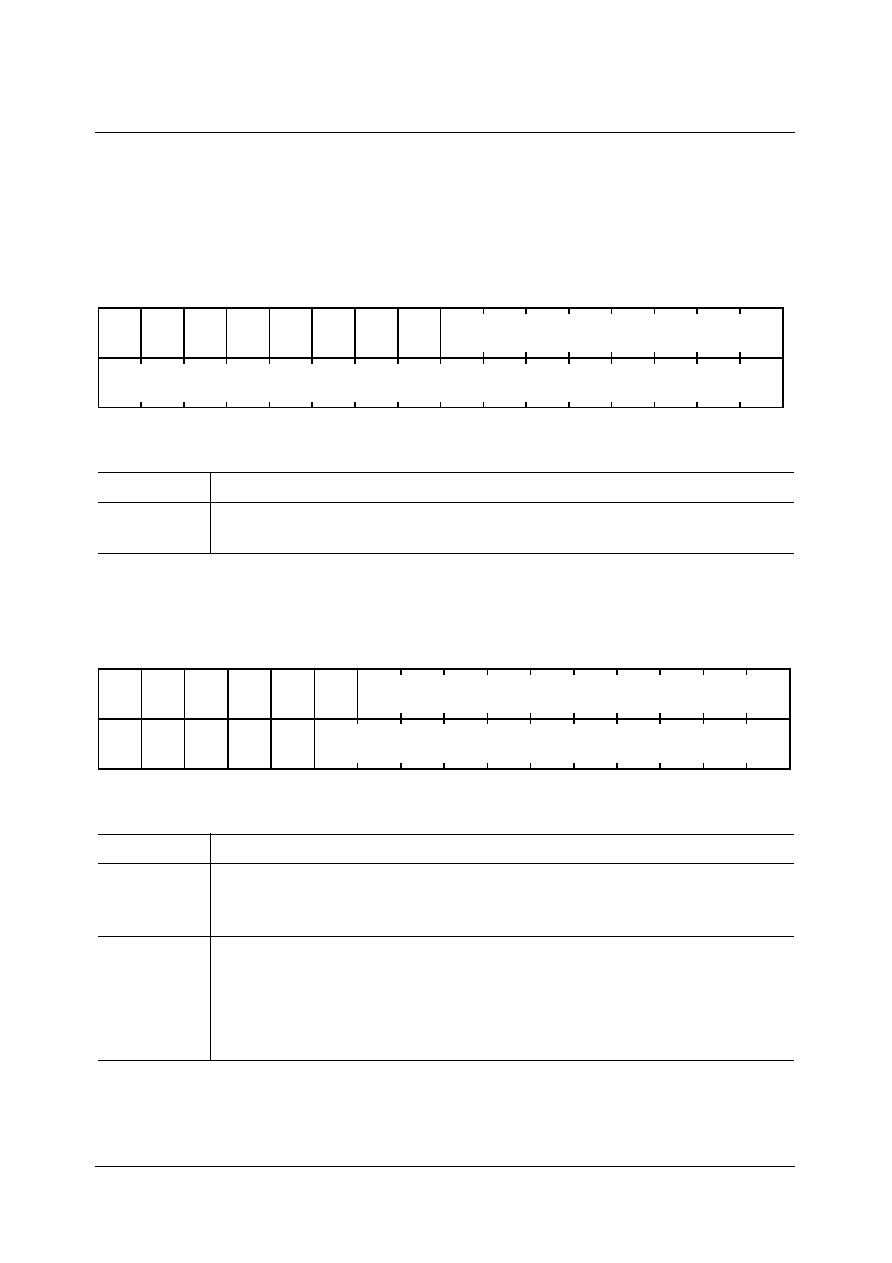
SDA 6000 / SDA 6001
PRELIMINARY DATA SHEET
Version 3.00
Display Generator
10 - 39
Micronas
10.7.4
Startaddress of Layer 2 (DBR)
The start address of frame buffer 2 in the memory must be set by the controller.
DBR
10.7.5
Size of Layer 2 (DSR)
DSR
Bit
Function
DB_ADDR
(23 ... 0)
Startaddress of Frame Buffer 2
Bit 23 ... 0 of a byte address.
Bit
Function
HEIGHT_L2
(9 ... 0)
Height of Layer 2
The height of layer 2 can vary between 0 (HEIGHT_L2 = `0'
d
) and 1023
pixels (HEIGHT_L2 = `1023'
d
).
WIDTH_L2
(10 ... 0)
Width of Layer 2
The width of the layer 2 can vary between 0 (WIDTH_L2 = `0'
d
) and
2046 pixels (WIDTH_L2 = `2046'
d
).
Note: Width_L2 is ignored, if layer 2 is displayed in 2-bit CLUT2 vector
format. In this case width_L2 is set to 64.
31
30
29
28
27
26
25
24
23
22
21
20
19
18
17
16
15
14
13
12
11
10
9
8
7
6
5
4
3
2
1
0
DB_ADDR(15..0)
1
-
-
-
DB_ADDR(23..16)
1
0
0
-
31
30
29
28
27
26
25
24
23
22
21
20
19
18
17
16
15
14
13
12
11
10
9
8
7
6
5
4
3
2
1
0
-
WIDTH_L2
-
-
-
-
1
-
HEIGHT_L2
1
0
1
-
SDA 6000 / SDA 6001
PRELIMINARY DATA SHEET
Version 3.00
Display Generator
10 - 40
Micronas
10.7.6
Display Coordinates of Layer 2 (DCR)
This instruction is used to place layer 2 in layer 1. By these coordinates the left top corner
of layer 2 is placed in relation to the top left corner of layer 1. In this sense the coordinate
ULY = 0/ULX = 0 is identical to the top left corner of layer 1. Negative coordinates are
also supported so it is also possible to move a layer 2 window from the top or left side of
a layer 1 window.
DCR
Bit
Function
ULY
(10 ... 0)
Upper left corner Y-coordinate
in one's complement representation:
`11111111111' = `� 1023
D
'
...
`10000000000' = `� 0
D
'
`00000000000' = `+ 0
D
'
...
`01111111111' = `+ 1023
D
'
ULX
(11 ... 0)
Upper left corner X-coordinate
in one's complement representation:
`111111111111' = `� 2046
D
'
...
`100000000000' = `� 0
D
'
`000000000000' = `+ 0
D
'
...
`011111111111' = `+ 2046
D
'
31
30
29
28
27
26
25
24
23
22
21
20
19
18
17
16
15
14
13
12
11
10
9
8
7
6
5
4
3
2
1
0
-
-
-
-
ULX(11..0)
0
1
1
0
-
ULY(10..0)

SDA 6000 / SDA 6001
PRELIMINARY DATA SHEET
Version 3.00
Display Generator
10 - 41
Micronas
10.7.7
Contents of CLUT (CLR)
CLR instruction allows the contents of the CLUT1 and CLUT2 to be set.
CLR
10.7.8
Clipping Coordinates (CUR and CBR)
These GAIs are used to set clipping coordinates for memory transfers. The clipping
coordinates describe a rectangle area in the destination memory area. During a memory
transfer these `clipped' memory areas are excluded from the transfer. The CUR
instruction is used to set the clipping start address. The CBR instruction is used to set
the width and height of the clipping area in amounts of pixels. A width of `0' means that
no clipping is processed, a width of `1' means the clipping area has the width of 1
pixel, .... A height of `0' means, that no clipping is processed, a height of `1' means the
clipping area has the height of 1 line, ... . Next to the start address, height and width a
clipping offset must be given for clipping. For a rectangle clipping area the sum of this
clipping offset and the clipping width must be the same as the sum of the destination area
width and the destination offset. Otherwise the clipping area will be a parallelogram, not
a rectangle.
Within instruction TAR it is decided whether the clipping area is inverted or non inverted.
Thus the outside region of the defined rectangle can be used for clipping as well as the
inside region. Please also refer to Chapter 10.5.2.
Bit
Function
CLUT_
ADDR
(8 ... 0)
CLUT address
Bits 7 ... 0 are CLUT vectors of either CLUT1 or CLUT2. Bit 8 selects the
CLUT:
0:
CLUT1 (256
�
16 bit)
1:
CLUT2 (256
�
14 bit)
CLUT_
CONTENT
(15 ... 0)
Contents to be written
to one of the look up tables addressed by the CLUT vector defined
above. For CLUT1 all the 16 bits are used, for CLUT2 only bits 13 ... 0
are used.
31
30
29
28
27
26
25
24
23
22
21
20
19
18
17
16
15
14
13
12
11
10
9
8
7
6
5
4
3
2
1
0
CLUT_CONTENT(15..0)
0
-
-
CLUT_ADDR(8..0)
1
1
1
-
SDA 6000 / SDA 6001
PRELIMINARY DATA SHEET
Version 3.00
Display Generator
10 - 42
Micronas
CUR
CBR
Bit
Function
C_OFFSET
(3 ... 0)
Clipping Offset (Bit3 ... 0)
The MSBs of C_OFFSET are defined by instruction CBR
CLIPPING
_ADDR
(23 ... 0)
Beginning of the clipping area
Bit 23 ... 0 of a byte address.
Bit
Function
HEIGHT_
CLIP
(9 ... 0)
Height of the clipping area
The height of the clipping area can vary between 0 (HEIGHT_CLIP = `0
d
')
and 1023 pixels (HEIGHT_CLIP = `1023
d
').
C_OFFSET
(10 ... 4)
Clipping Offset (Bit 10 ... 4)
The LSBs of C_OFFSET are defined by instruction CUR.
WIDTH_
CLIP
(10 ... 0)
Width of the clipping area
The width of the clipping area can vary between 0 (WIDTH_CLIP = `0
d
')
and 2046 pixels (WIDTH_CLIP = `2046
d
').
31
30
29
28
27
26
25
24
23
22
21 20
19
18
17
16
15
14
13
12
11
10
9
8
7
6
5
4
3
2
1
0
CLIPPING_ADDR(15..0)
0
CLIPPING_ADDR(23..16)
0
0
0
C_OFFSET(3..0)
31
30
29
28
27
26
25
24
23
22
21
20
19
18
17
16
15
14
13
12
11
10
9
8
7
6
5
4
3
2
1
0
WIDTH_CLIP(10..0)
C_OFFSET(8..4)
0
C_OFFSET
(10..9)
0
0
1
HEIGHT_CLIP(9..0)
SDA 6000 / SDA 6001
PRELIMINARY DATA SHEET
Version 3.00
Display Generator
10 - 43
Micronas
10.7.9
Source Descriptor for Data Transfer (SDR)
This instruction defines the beginning of the memory area to be read and transferred.
SDR
This instruction defines the beginning of the destination memory area.
DDR
Bit
Function
GO
Must be set to `1' if GA is to start memory transfer after executing this
GA-instruction. Otherwise this bit must be set to `0'.
S_ADDR
(23 ... 0)
Start address of memory area to be transferred.
Bit 23 ... 0 of a byte address.
Bit
Function
GO
Must be set to `1' if GA is to start memory transfer after executing this
GA-instruction. Otherwise this bit must be set to `0'.
D_ADDR
(23 ... 0)
Beginning of the destination memory area
Bit 23 ... 0 of a byte address.
31
30
29 28
27
26
25
24
23
22
21
20
19
18
17
16
15
14
13
12
11
10
9
8
7
6
5
4
3
2
1
0
S_ADDR(15..0)
1
-
-
-
S_ADDR(23..16)
0
0
0
GO
31
30
29
28
27
26
25
24
23
22
21
20
19
18
17
16
15
14
13
12
11
10
9
8
7
6
5
4
3
2
1
0
D_ADDR(15..0)
1
-
-
-
D_ADDR(23..16)
0
0
1
GO
SDA 6000 / SDA 6001
PRELIMINARY DATA SHEET
Version 3.00
Display Generator
10 - 44
Micronas
10.7.10
Source Size of Transferred Memory Area (TSR)
This register contains different information depending on transfer mode. The size of
transferred memory is described by width and height of the source of the transfer area.
Please also refer to Chapter 10.5.2.
TSR
Bit
Function
GO
Must be set to `1' if GA is to start memory transfer after executing this
GA-instruction. Otherwise this bit must be set to `0'.
WIDTH_IN
(10 ... 0)
Width of the transferred area in count of pixels.
WIDTH_IN = `0': No transfer will be executed.
31
30
29
28
27
26
25
24
23 22
21 20
19
18
17
16
15
14
13
12
11
10
9
8
7
6
5
4
3
2
1
0
-
WIDTH_IN(10..0)
-
-
-
-
0
-
-
-
-
-
-
-
-
-
-
-
0
1
0
GO
SDA 6000 / SDA 6001
PRELIMINARY DATA SHEET
Version 3.00
Display Generator
10 - 45
Micronas
10.7.11
Destination Size of Transferred Memory Area (TDR)
TDR
Bit
Function
GO
Must be set to `1' if GA is to start memory transfer after executing this
GA-instruction. Otherwise this bit must be set to `0'.
HEIGHT_
OUT
(9 ... 0)
Height of the transferred area in count of pixels
HEIGHT_OUT = `0': No transfer will be executed.
WIDTH_
OUT
(10 ... 0)
Width of the transferred area in count of pixels
WIDTH_OUT = `0': No transfer will be executed.
31
30
29
28
27
26
25
24
23
22
21
20
19
18
17 16
15
14
13
12
11
10
9
8
7
6
5
4
3
2
1
0
-
WIDTH_OUT(10..0)
-
-
-
-
0
-
HEIGHT_OUT(9..0)
0
1
1
GO
SDA 6000 / SDA 6001
PRELIMINARY DATA SHEET
Version 3.00
Display Generator
10 - 46
Micronas
10.7.12
Offset of Transferred Memory Area (TOR)
This instruction defines the offset value for rectangle memory transfers.
TOR
Bit
Function
GO
Must be set to `1' if GA is to start memory transfer after executing this
GA-instruction. Otherwise this bit must be set to `0'.
S_OFFSET
(10 ... 0)
Source offset value for non linear transfer
For more information about S_OFFSET refer to Chapter 10.5.2.
D_OFFSET
(10 ... 0)
Destination offset value for non linear transfer
For more information about D_OFFSET refer to Chapter 10.5.2.
31
30
29
28
27
26
25
24
23
22
21
20
19
18 17
16
15
14
13
12
11
10
9
8
7
6
5
4
3
2
1
0
-
S_OFFSET(10..0)
-
-
-
-
1
D_OFFSET(10..0)
0
1
0
GO

SDA 6000 / SDA 6001
PRELIMINARY DATA SHEET
Version 3.00
Display Generator
10 - 47
Micronas
10.7.13
Attributes of Transfer (TAR)
This instruction defines the transfer mode.
TAR
Table 10-7
Bit
Function
GO
Must be set to `1' if GA is to start memory transfer after executing this
GA-instruction. Otherwise this bit must be set to `0'.
TQH
Quadruple Height during Transfer
`0':
Normal height is selected.
`1'
The memory transfer is stretched in vertical direction on the output
side.
UN
Underline on/off
0:
Underline is switched off.
1:
The last line (independent from `TDH') in the destination area is
filled with a constant CLUT1 input (vector 0 of CLUT1) instead of
the source bitmap input.
CL
(1 ... 0)
Clipping on/off
00: Clipping is switched off.
01: Reserved.
10: Clipping is switched on. Pixels within the clipping area will be
affected.
11: Clipping is switched on. Pixels outside the clipping area will be
affected.
TRM
Transparency Mode for Transfer
`0':
The complete area defined by instruction SDR and TDR is written
to the destination.
`1':
Only these (4:4:4:2) pixels are written to the destination area, for
which Bit TR1 = `0'.
Note: This bit is only relevant for 16-bit (4:4:4:2) RGB output formats
Please also refer to Chapter 10.5.1.
31
30
29
28
27
26
25
24
23
22
21
20
19
18
17
16
15
14
13
12
11
10
9
8
7
6
5
4
3
2
1
0
UN
TRM
TMODE(4..0)
IT
TDW
TDH
FLA(1..0)
-
TQH
CL(1..0)
1
-
-
-
-
-
-
-
-
-
-
-
0
1
1
GO

SDA 6000 / SDA 6001
PRELIMINARY DATA SHEET
Version 3.00
Display Generator
10 - 48
Micronas
TMODE
(4 ... 0)
Transfer Mode
This mode is used to decide which transfer mode should be used. With
this bit it is decided which input and which output format is used for
transformation. For detailed information of the register settings please
refer to Chapter 10.5.1
IT
Italic
This bit is used in transfer modes if 16-bit (4:4:4:2) RGB output mode is
selected.
`0':
Italic is switched off.
`1':
Italic mode is enabled.
TDW
Double Width during Transfer
`0':
Normal width is selected.
`1':
The memory transfer is stretched in horizontal direction on the
output side.
TDH
Double Height during Transfer
`0':
Normal height is selected.
`1'
The memory transfer is stretched in vertical direction on the output
side. TQH must be set to `0'.
FLA(1 ... 0)
Flash Definition
This bit is used in transfer modes if output mode is in 16-bit (4:4:4:2)
format for TTX. This bit is used to replace one of the 16 output bits.
Please refer to Chapter 10.5.1. Bits Flash (1 ... 0) describe the flash
phase for memory transfer modes:
`00': slow rate (1 Hz)
`01': Fast rate flash (2 Hz) Phase 1
`10': Fast rate flash (2 Hz) Phase 2
`11': Fast rate flash (2 Hz) Phase 3
Table 10-7
(cont'd)
Bit
Function

SDA 6000 / SDA 6001
PRELIMINARY DATA SHEET
Version 3.00
Display Generator
10 - 49
Micronas
10.8
Digital RGB interface
10.8.1
General
The digital RGB color components generated by the display generator are converted to
analog voltage values by D/A converters on silicon.
However there are peripherals and display units in the market which are not capable to
process those analog RGB components. To interconnect with these devices SDA6000
provides the flexibility to use different ports as a output of digital RGB components. After
reset the digital RGB interface is disabled and must be enabled for each single pin. If
enabled, the secondary function and the original function of the pin are completly
overruled by the digital RGB interface function. For more information regarding the
secondary and original function of the pins (refer also to Chapter 6.10).
Depending on the display mode, for the red and the blue component maximum 5 bits
(bit1 to bit5 of internal D/A converter input) are available. For the green component
maximum 6 bits (bit0 to bit5 of internal D/A converter input) are avilable.
Furthermore SDA6000 is flexible enough to work
� with a external pixel clock
or
� to generate the pixel clock internally and provide this clock to external devices
For the pixel clock input and output functionality Pin77 is used.

SDA 6000 / SDA 6001
PRELIMINARY DATA SHEET
Version 3.00
Display Generator
10 - 50
Micronas
10.8.2
Ports used for digital RGB Interface
Following ports are used for the digital interface:
Table 10-8
Pin Definition for digital RGB interface
Pin
No.
Pin Name
Second
Function
digital RGB interface function
77
P3.3
T3OUT
pixel clock input and output clk_px_i/clk_px_o
78
P3.4
T3EUD
bit 1 of internal D/A-input for red r_o1
79
P3.5
T4IN
bit 2 of internal D/A-input for red r_o2
80
P3.6
T3IN
bit 3 of internal D/A-input for red r_o3
81
P3.7
T2IN
bit 4 of internal D/A-input for red r_o4
90
P3.12
-
bit 5 of internal D/A-input for red r_o5
92
P3.15
-
bit 0 of internal D/A-input for green g_o0
93
P5.14
T4EUD
bit 1 of internal D/A-input for green g_o1
94
P5.15
T2EUD
bit 2 of internal D/A-input for green g_o2
95
P6.0
TRIG_IN
bit 3 of internal D/A-input for green g_o3
96
P6.1
TRIG_OUT bit 4 of internal D/A-input for green g_o4
97
P6.2
FIELD
(only B11)
bit 5 of internal D/A-input for green g_o5
6
P2.9
EX1IN
bit 1 of internal D/A-input for blue b_o1
7
P2.10
EX2IN
bit 2 of internal D/A-input for blue b_o2
8
P2.11
EX3IN
bit 3 of internal D/A-input for blue b_o3
9
P2.12
EX4IN
bit 4 of internal D/A-input for blue b_o4
10
P2.13
EX5IN
bit 5 of internal D/A-input for blue b_o5

SDA 6000 / SDA 6001
PRELIMINARY DATA SHEET
Version 3.00
Display Generator
10 - 51
Micronas
10.8.3
Registers used for the digital RGB interface
RGBINTFC_EN
Reset Value: 0000
H
Bit
Function
R_EN1
RED component bit 1 enable of digital RGB interface
0: original/secondary function of pin 78 enabled (refer also to
Chapter 6.10)
1: digital RGB interface function of pin 78 enabled
R_EN2
RED component bit 2 enable of digital RGB interface
0: original/secondary function of pin 79 enabled (see also 6.10)
1: digital RGB interface function of pin 79 enabled
R_EN3
RED component bit 3 enable of digital RGB interface
0: original/secondary function of pin 80 enabled (refer also to
Chapter 6.10)
1: digital RGB interface function of pin 80 enabled
R_EN4
RED component bit 4 enable of digital RGB interface
0: original/secondary function of pin 81 enabled (refer also to
Chapter 6.10)
1: digital RGB interface function of pin 81 enabled
R_EN5
RED component bit 5 enable of digital RGB interface
0: original/secondary function of pin 90 enabled (refer also to
Chapter 6.10)
1: digital RGB interface function of pin 90 enabled
G_EN0
GREEN component bit 0 enable of digital RGB interface
0: original/secondary function of pin 92 enabled (refer also to
Chapter 6.10)
1: digital RGB interface function of pin 92 enabled
G_EN1
GREEN component bit 1 enable of digital RGB interface
0: original/secondary function of pin 93 enabled (refer also to
Chapter 6.10)
1: digital RGB interface function of pin 93 enabled
5
4
3
2
1
0
11
10
9
8
7
6
15
14
13
12
B_EN
2
B_EN
1
B_EN
3
B_EN
4
B_EN
5
G_EN
5
G_EN
4
G_EN
3
R_EN
3
R_EN
2
R_EN
1
G_EN
2
G_EN
1
G_EN
0
R_EN
5
R_EN
4
rw
rw
rw
rw
rw
rw
rw
rw
rw
rw
rw
rw
rw
rw
rw
rw

SDA 6000 / SDA 6001
PRELIMINARY DATA SHEET
Version 3.00
Display Generator
10 - 52
Micronas
G_EN2
GREEN component bit 2 enable of digital RGB interface
0: original/secondary function of pin 94 enabled (refer also to
Chapter 6.10)
1: digital RGB interface function of pin 94 enabled
G_EN3
GREEN component bit 3 enable of digital RGB interface
0: original/secondary function of pin 95 enabled (refer also to
Chapter 6.10)
1: digital RGB interface function of pin 95 enabled
G_EN4
GREEN component bit 4 enable of digital RGB interface
0: original/secondary function of pin 96 enabled (refer also to
Chapter 6.10)
1: digital RGB interface function of pin 96 enabled
G_EN5
GREEN component bit 5 enable of digital RGB interface
0: original/secondary function of pin 97 enabled (refer also to
Chapter 6.10)
1: digital RGB interface function of pin 97 enabled
B_EN1
BLUE component bit 1 enable of digital RGB interface
0: original/secondary function of pin 6 enabled (refer also to
Chapter 6.10)
1: digital RGB interface function of pin 6 enabled
B_EN2
BLUE component bit 2 enable of digital RGB interface
0: original/secondary function of pin 7 enabled (refer also to
Chapter 6.10)
1: digital RGB interface function of pin 7 enabled
B_EN3
BLUE component bit 3 enable of digital RGB interface
0: original/secondary function of pin 8 enabled (refer also to
Chapter 6.10)
1: digital RGB interface function of pin 8 enabled
B_EN4
BLUE component bit 4 enable of digital RGB interface
0: original/secondary function of pin 9 enabled (refer also to
Chapter 6.10)
1: digital RGB interface function of pin 9 enabled
B_EN5
BLUE component bit 5 enable of digital RGB interface
0: original/secondary function of pin 10 enabled (refer also to
Chapter 6.10)
1: digital RGB interface function of pin 10 enabled
Bit
Function

SDA 6000 / SDA 6001
PRELIMINARY DATA SHEET
Version 3.00
Display Generator
10 - 53
Micronas
CLKINTFC_EN
Reset Value: 0000
H
Bit
Function
CLK_EN
Pixel clock input/output enable
This bit is used to enable the clock input/output functionality of pin 77
0: original/secondary function of pin 77 enabled (refer also to
Chapter 6.10)
1: pixel clock input/output of pin 77 enabled
CLK_IO
Switching pixel clock input/output
Used to decide if pin77 is used for pixel clock input or for pixel clock out-
put.
This bit is only used if pixel clock input/output is enabled by bit CLK_EN.
0: Pin 77 used as output (if enabled by CLK_EN)
1: Pin 77 used as input (if enabled by CLK_EN)
5
4
3
2
1
0
11
10
9
8
7
6
15
14
13
12
-
-
-
-
-
-
-
CLK_
IO
CLK_
EN
-
-
-
-
-
rw
rw
-
-

D/A Converter

SDA 6000 / SDA 6001
PRELIMINARY DATA SHEET
Version 3.00
D/A Converter
11 - 3
Micronas
11
D/A Converter
M2 uses a 3
�
6-bit voltage D/A converter to generate analog RGB output signals with a
nominal amplitude of 0.7 V (also available: 0.5 V, 1.0 V and 1.2 V) peak to peak. Two
different modes are available in order to allow the reduction of power consumption for
applications which require a lower RGB bandwidth.

SDA 6000 / SDA 6001
PRELIMINARY DATA SHEET
Version 3.00
D/A Converter
11 - 4
Micronas
11.1
Register Description
DACCON
Reset Value: 0005
H
Bit
Function
RGBGAIN
(1 ... 0)
Gain Adjustment of RGB Converter.
The user can change the output gain of the DAC.
00:
0.5 V
01:
0.7 V
10:
1.0 V
11:
1.2 V
BWC
Bandwidth Control
0:
The effective bandwidth of the DAC is set to 50 MHz
1:
The effective bandwidth of the DAC is set to 32 MHz. This reduces
the current consumption of analog supply.
5
4
3
2
1
0
11
10
9
8
7
6
15
14
13
12
rw
rw
-
-
-
-
-
-
-
-
-
-
-
-
-
BWC
RGBGAIN
(1..0)

Slicer and Acquisition

SDA 6000 / SDA 6001
PRELIMINARY DATA SHEET
Version 3.00
Slicer and Acquisition
12 - 3
Micronas
12
Slicer and Acquisition

SDA 6000 / SDA 6001
PRELIMINARY DATA SHEET
Version 3.00
Slicer and Acquisition
12 - 4
Micronas
12.1
General Function
M2 provides a full digital slicer including digital H- and V-sync separation and digital sync
processing. The acquisition interface is capable to process on all known data services
starting from line 6 to line 23 for TV (Teletext, VPS, CC, G+, WSS) as well as any full
channel services. Four different framing codes (two of them programmable from field to
field) are available for each field. Digital signal processing algorithms are applied to
compensate various disturbance mechanisms. These are:
� Noise measurement and compensation.
� Attenuation measurement and compensation.
� Group delay measurement and compensation.
Note: Thus, M2 is optimized for precise data clock recovery and error free reception of
data widely unaffected from noise and the currently valid channel characteristics.
Two slicers with separated A/D converters and separated CVBS inputs are
implemented. The first one is a full service slicer. The second one is a slicer which
supports only the capturing of WSS data. Both CVBS inputs contain an on-chip clamping
circuit. The integrated A/D converters are 7 bit video converters running at the internal
frequency of 33.33 MHz.
The sliced data is synchronized to the frequency of the clock-run-in of the actual data
service and to the framing code of the data stream, framing code checked and written to
a programmable VBI buffer in the external memory. After line 23 is received an interrupt
can be given to the microcontroller. The microcontroller starts to process the data of this
buffer. That means, the data is error checked by software and stored in the memory in
the appropriate data base format.
To improve the signal quality the slicer control logic generates horizontal and vertical
windows in which the reception of the framing code is allowed. The framing code can be
programmed for each line individually, so that in each line a different service can be
received. For VPS and WSS the framing code is hardwired. In a special mode the
framing code can be bypassed, so that all incoming data will be stored in the VBI buffer.
The framing code check can then be made by software. All following acquisition tasks
are performed by the internal controller, so in principal the data of every data service can
be acquired.

SDA 6000 / SDA 6001
PRELIMINARY DATA SHEET
Version 3.00
Slicer and Acquisition
12 - 5
Micronas
12.2
Slicer Architecture
The slicer is composed of five main blocks:
� The full service slicer (Slicer 1)
� The WSS only slicer (Slicer 2)
� The H/V synchronization for full service slicer (Sync 1)
� The H/V synchronization for WSS only slicer (Sync 2)
� The acquisition interface
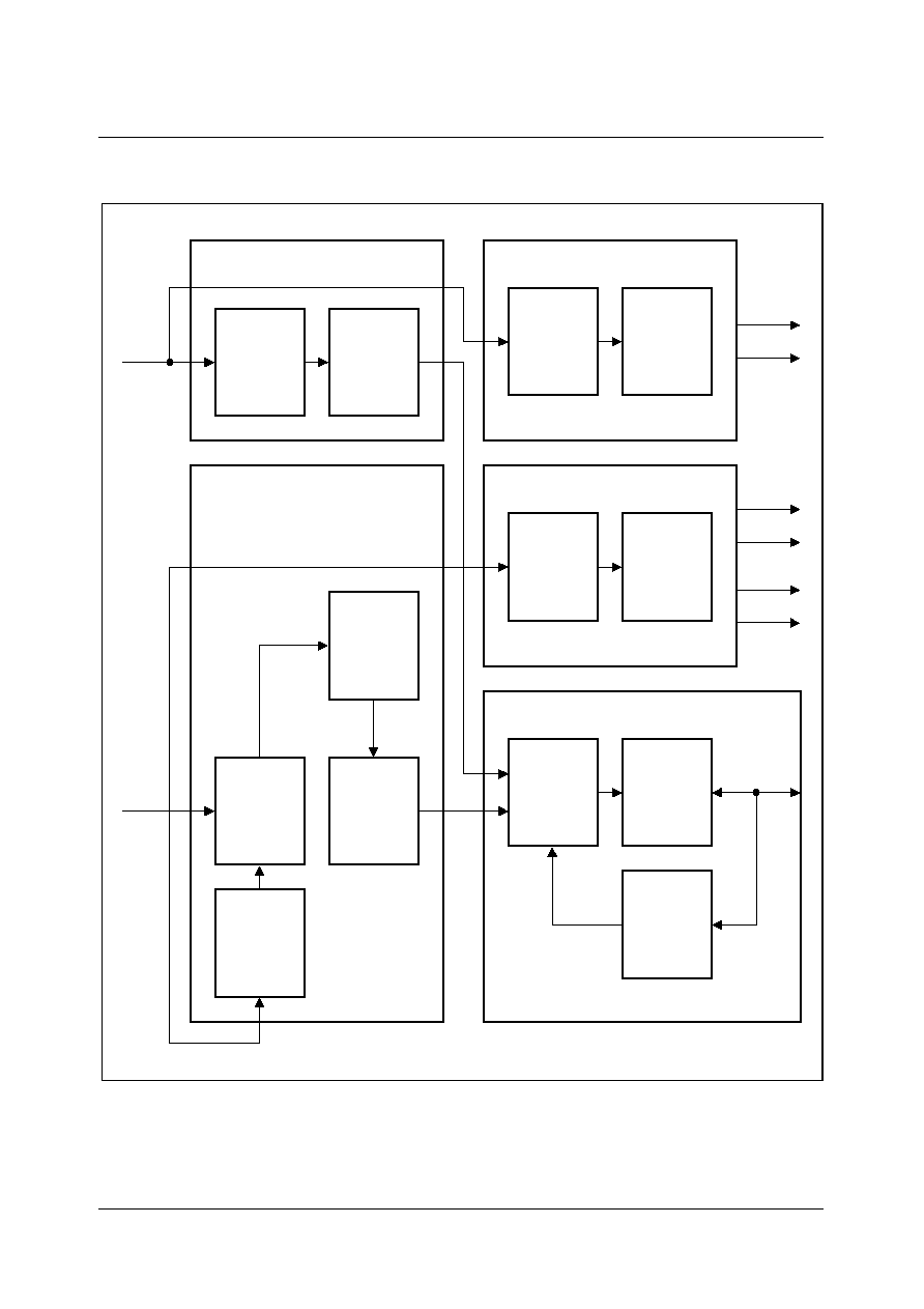
SDA 6000 / SDA 6001
PRELIMINARY DATA SHEET
Version 3.00
Slicer and Acquisition
12 - 6
Micronas
Figure 12-1 Block Diagram of Digital Slicer and Acquisition Interface
UEB11191
D-PLL
Separation
Data
Slicer 2
(WSS only Slicer)
Sync 2
H-PLL
Timing
Sync
H/V
+
Sep.
CVBS2
HS2_IR
VS2_IR
Sync 1
Sync
Timing
Sep.
+
H/V
H-PLL
CC_IR
L23_IR
HS1_IR
VS1_IR
Acquisition Interface
(Full Service Slicer)
Slicer 1
&
S/P
Converter
FC-Check
Address
Generation
Buffer
Parameter
To/from
Memory
D-PLL
Separation
Data
Compen.
Noise
Group-D.
Attenua.
Measur.
Group-D.
Attenua.
Noise
CVBS1

SDA 6000 / SDA 6001
PRELIMINARY DATA SHEET
Version 3.00
Slicer and Acquisition
12 - 7
Micronas
12.2.1
Distortion Processing
For the full service slicer the digital bit stream is applied to a circuitry which corrects
transmission distortion. In order to apply the correct counter-measures, a signal
evaluation is done in parallel. This measurement device can detect and compensate the
following distortions:
- noise
- frequency attenuation
- group delay

SDA 6000 / SDA 6001
PRELIMINARY DATA SHEET
Version 3.00
Slicer and Acquisition
12 - 8
Micronas
12.3
H/V-Synchronization
Slicer and acquisition interface need many signals synchronized to the incoming CVBS
(e.g. line number, field or line start). Therefore a sync slicing level is calculated and the
sync signal is sliced from the filtered digital CVBS signal. Using digital integration vertical
and horizontal sync pulses are separated. The horizontal pulses are fed into a digital H-
PLL which has flywheel functionality. The H-PLL includes a counter which is used to
generate all the necessary horizontal control signals. The vertical sync is used to
synchronize the line counter from which the vertical control signals are derived.
The synchronization block includes a watchdog which keeps control of the actual lock
condition of the H-PLL.The watchdog can produce an interrupt (CC_IR) if
synchronization has been lost. It could therefore be an indication for a channel change
or missing input signal.
Note: This H/V synchronization for the slicer 2 uses the same algorithms as described
above.

SDA 6000 / SDA 6001
PRELIMINARY DATA SHEET
Version 3.00
Slicer and Acquisition
12 - 9
Micronas
12.4
Acquisition Interface
The acquisition interface manages the data transfer between both slicers and memory.
First of all a byte synchronization is performed (FC-check). Following this, the data is
paralleled and shifted into memory as 16 bit words. In the other direction parameters are
loaded from memory to the slicer. After every vertical sync, parameters needed for the
field are downloaded and after every horizontal sync line parameters are downloaded.
The parameters are used for slicer configuration.
The data acquisition supports several features. The FC-checker is able to handle four
different framing codes for one field. Two of these framing codes are programmable and
could therefore be changed from field to field. The acquisition can be switched from
normal mode (line 6 to 23) to full channel mode (line 6 to end of field).
12.4.1
FC-Check
There are four FC's which are compared to the incoming signal. The first one is 8-bit wide
and is loaded down with the field parameters. The second one is 16-bit wide and fixed
to the FC of VPS. The third one is also 16-bit wide, but can be loaded with the field
parameters. If the third one is used, the user can specify not only the FC but also a don't-
care mask. The fourth FC is reserved for WSS. The actual FC can be changed line by
line.
FC1
This FC should be used for all services with 8-bit framing codes (e.g. for TTX). The actual
framing code is loaded down each field. The check can be done without any error
tolerance or with a one bit error tolerance.
Note: If FC1 = E4
H
this pattern is used as a reference for group delay measurement.
FCVPS
This FC is fixed to that of VPS. Only an error free signal will enable the reception of the
VPS data line.
Note: If VPS should be sliced in field 1 and TTX in field 2 the appropriate line parameters
for line 16 have to be dynamically changed from field to field.
FC3
This 16-bit framing code is loaded with the field parameters as well as a don't care mask.
The incoming signal is compared to both, framing code and don't care mask. Further
reception is enabled if all bits, which are not don't care, match the incoming data stream.

SDA 6000 / SDA 6001
PRELIMINARY DATA SHEET
Version 3.00
Slicer and Acquisition
12 - 10
Micronas
FCWSS
This FC is fixed to that of WSS. A special algorithm makes sure that the WSS-FC is
detected even if the CVBS signal is coming from a video tape.
No FC-check
If FC-check is disabled, the data recording is triggered by the data start recognition. In
this case the software needs to do the byte synchronization.
FC-Check Select
There is a two bit line parameter called FCSEL. With this parameter the user will be able
to select which FC-Check is used for the actual line. If NORM is set to WSS the WSS
FCcheck is used independently of FCSEL.
12.4.2
Interrupts
Some events which occur inside the slicer, the sync separation or the acquisition
interface can be used to trigger an interrupt. They are summarized in register ACQISN.
The hardware sets the associated interrupt flag which must be manually reset by SW
before the next interrupt can be accepted. All ACQ interrupts are bundled into one
interrupt which is fed to the ACQ-interrupt node (ACQIC) of the controller.
12.4.3
VBI Buffer and Memory Organization
Slicer and acquisition interface need parameters for configuration and they produce
status information for the CPU.
Some of these parameters and status bits are constant for a field. Those parameters are
called field parameters. They are downloaded after the vertical sync of slicer 1. If the
synchronization of slicer 1 is missing the vertical sync from slicer 2 is used to initialize
the parameter download.
Other parameters and status bits may change from line to line (e.g. data service
dependent values). Those parameters are called line parameters. They are downloaded
after each horizontal sync.
The start address of the VBI (VBI = vertical blanking interval) buffer can be configured
with special function register `STRVBI'. 32 16-bit words have to be reserved for every
sliced data line. If 18 (in full channel mode 350) lines of data have been sent to memory
no further acquisition takes place until the next vertical pulse appears and the H-PLL is
still locked. That means if at least 1176 Bytes (22424 Bytes in full channel mode) are
reserved for the VBI buffer no VBI overflow is possible. The acquisition can be started
and stopped by the controller using bit `ACQON' of register STRVBI. The acquisition is
stopped as soon as this bit changed to `0'. If the bit is changed back to `1' switching on
of the acquisition is synchronized to the next V-pulse. The start address (Bit 13 ... 0 of

SDA 6000 / SDA 6001
PRELIMINARY DATA SHEET
Version 3.00
Slicer and Acquisition
12 - 11
Micronas
register STRVBI) of the VBI buffer should only be changed if the acquisition is switched
off.
SDA 6000 / SDA 6001
PRELIMINARY DATA SHEET
Version 3.00
Slicer and Acquisition
12 - 12
Micronas
Figure 12-2 VBI Buffer: General Structure
15
Byte 0
Byte 1
ACQFP0
ACQFP1
ACQFP2
ACQFP3
ACQFP4
ACQFP5
send to slicer
after V-Sync
write to memory
after V-Sync
STRVBI
Line Status
ACQLP0
ACQLP1
send to slicer
after H-Sync
send to memory
after detecting
a FC
additional line
status information
VBI start line 6
send to slicer
after H-Sync
VBI start line 7
ACQLP0
ACQLP1
Line Status
and so on
32
16bit
words
databyte 1
databyte 0
databyte 2
databyte 3
databyte 4
data
data
data
data
data
data
data
data
data
data
data
data
ACQLP4
ACQLP4
ACQFP6
0
databyte 5
Field Status Information from both Slicers
Sliced WSS Data (Slicer 2)
Sliced WSS Data (Slicer 2)
Sliced WSS Data (Slicer 2)
Sliced WSS Data (Slicer 2)
Sliced WSS Data (Slicer 2)
Field Status Information from both Slicers
Line Parameters for Slicer 1
Line Parameters for Slicer 1
Line Parameters for Slicer 1
Line Parameters for Slicer 1
ACQFP7
ACQFP8
ACQFP9
Field Parameters
Field Parameters
Field Parameters
Sliced WSS Data (Slicer 2)
ACQFP10
send to memory
after detecting
a FC
ACQFP2b
Field Parameters
Line Parameters for Slicer 1
Line Parameters for Slicer 1
ACQLP2
ACQLP3
ACQLP5
Line Status
ACQLP2
ACQLP3
Line Parameters for Slicer 1
Line Parameters for Slicer 1

SDA 6000 / SDA 6001
PRELIMINARY DATA SHEET
Version 3.00
Slicer and Acquisition
12 - 13
Micronas
12.5
Register Description
The acquisition interface has the following SFR Registers. The line and field parameters
are stored in the RAM (RAM Registers). They have to be initialized by software before
starting the acquisition.
Special Function Registers:
STRVBI
Reset Value: 0400
H
HSGL_WIN
Reset Value: 0000
H
Bit
Function
ACQON
Enable Acquisition
0:
The ACQ interface does not access memory (immediately
inactive)
1:
The ACQ interface is active and writes data to memory (switching
on is synchronous to V)
VBIADR
(23 ... 10)
Define the 14 MSB's of the start address of the VBI buffer.
The VBI buffer location can be aligned with any 1 KByte memory
segment.
5
4
3
2
1
0
11
10
9
8
7
6
15
14
13
12
VBIADR(23..10)
ACQ
ON
0
rw
rw
rw
rw
rw
rw
rw
rw
rw
rw
rw
rw
rw
rw
rw
5
4
3
2
1
0
11
10
9
8
7
6
15
14
13
12
0
0
0
0
0
0
0
0
0
0
0
0
HSGL_WIN
rw
rw
rw
rw
SDA 6000 / SDA 6001
PRELIMINARY DATA SHEET
Version 3.00
Slicer and Acquisition
12 - 14
Micronas
EN_ACQPARAM
Reset Value: 0000
H
ACQISN
Reset Value: 0000
H
Bit
Function
HSGL_WIN
(3 ... 0)
Defines the width of the window for the acceptance of incoming H-sync
pulses
0000: +/- 1.92us
0001: +/- 3.84us
1111: +/- 30.072us
This parameter only effects the H-window if EN_HSGL_WIN = 1.
Bit
Function
EN_HSGL_
WIN
Enables the parameter HSGL_WIN.
0:parameter setting for HSGL_WIN irrelevant
1:parameter HSGL_WIN enabled
EN_GD_ME
AS
Enables the parameters GD_MEASP and GD_MEASN.
0:parameter settings for GD_MEASP and GD_MEASN irrelevant
1:parameters GD_MEASP and GD_MEASN enabled
EN_DATA_
STL
Switches between internal and external data-start-threshold
0:internal data start thresholds are used for both slicers
1:external (S1_dstl_sel and S2_dstl_sel) data start thresholds are used
EN_GD_CO
MP
Enables the parameter GD_COMP.
0:parameter setting for GD_COMP irrelevant
1:parameter GD_COMP enabled
5
4
3
2
1
0
11
10
9
8
7
6
15
14
13
12
0
0
0
0
0
0
0
EN_H
SGL_
WIN
EN_G
D_ME
AS
EN_D
ATA_
STL
EN_G
D_CO
MP
0
0
0
0
0
rw
rw
rw
rw
5
4
3
2
1
0
11
10
9
8
7
6
15
14
13
12
rw
rw
rw
rw
rw
rw
rw
rw
rw
rw
rw
rw
0
0
0
CC_IE
0
CC_IR L23_
IE
L23_
IR
HS2_
IE
HS2_
IR
VS2_
IE
VS2_
IR
HS1_
IE
HS1_
IR
VS1_
IE
VS1_
IR

SDA 6000 / SDA 6001
PRELIMINARY DATA SHEET
Version 3.00
Slicer and Acquisition
12 - 15
Micronas
Bit
Function
VS1_IR
VS interrupt. The vertical sync impulse can be used to have field
synchronization for the software. (VS of slicer 1 is used).
0: No
request
pending.
1:
This source has raised an interrupt request.
VS1_IE
Interrupt Enable Bit
0:
Disables the interrupt.
1:
Enables the interrupt.
HS1_IR
HS interrupt. The horizontal sync impulse can be used to implement a
software line counter. (HS of slicer 1 is used).
0: No
request
pending.
1:
This source has raised an interrupt request.
HS1_IE
Interrupt Enable Bit
0:
Disables the interrupt.
1:
Enables the interrupt.
VS2_IR
VS interrupt. The vertical sync impulse can be used to have field
synchronization for the software. (VS of slicer 2 is used).
0: No
request
pending.
1:
This source has raised an interrupt request.
VS2_IE
Interrupt Enable Bit
0:
Disables the interrupt.
1:
Enables the interrupt.
HS2_IR
HS interrupt. The horizontal sync impulse can be used to implement a
software line counter. (HS of slicer 2 is used).
0: No
request
pending.
1:
This source has raised an interrupt request.
HS2_IE
Interrupt Enable Bit
0:
Disables the interrupt.
1:
Enables the interrupt.
L23_IR
Line 23 Interrupt.Tells the controller that line 23 of the VBI is sliced
(Slicer 1 is used).
0: No
request
pending.
1:
This source has raised an interrupt request.
L23_IE
Interrupt Enable Bit
0:
Disables the interrupt.
1:
Enables the interrupt.
SDA 6000 / SDA 6001
PRELIMINARY DATA SHEET
Version 3.00
Slicer and Acquisition
12 - 16
Micronas
Note: The interrupt request flags of the ACQ interrupt subnode have to be cleared by
software within the interrupt service routine.
12.5.1
RAM Registers
Field Parameters
All field parameters are updated once in a field. This means that the status information
written from the acquisition interface to the memory at that time only represents a
snapshot of the status. Hardware ensures that field parameters are updated even if only
one of the two CVBS signals has a valid sync timing. So it is assured that even if CVBS1
is not available data of CVBS2 still can be sliced.
ACQFP0
Reset Value: XXXX
H
ACQFP1
Reset Value: XXXX
H
CC_IR
Channel Change Indicator
The H-PLL has lost the synchronization. (Slicer 1 is used).
0: No
request
pending.
1:
This source has raised an interrupt request.
Note: Also refer to status bits STAB1 or VDOK1
CC_IE
Interrupt Enable Bit
0:
Disables the interrupt.
1:
Enables the interrupt.
Bit
Function
FC3
(15 ... 0)
Framing code 3
Bit 15: First received bit of FC.
Bit 0: Last received bit of FC.
Bit
Function
5
4
3
2
1
0
11
10
9
8
7
6
15
14
13
12
FC3(15..0)

SDA 6000 / SDA 6001
PRELIMINARY DATA SHEET
Version 3.00
Slicer and Acquisition
12 - 17
Micronas
Bit
Function
FC3MASK
(15 ... 0)
Mask for Framing code 3
Bit 15:Mask for first received bit of FC.
Bit 0: Mask for last received bit of FC.
5
4
3
2
1
0
11
10
9
8
7
6
15
14
13
12
FC3MASK(15..0)

SDA 6000 / SDA 6001
PRELIMINARY DATA SHEET
Version 3.00
Slicer and Acquisition
12 - 18
Micronas
ACQFP2
Reset Value: XXXX
H
ACQFP2b
Reset Value: XXXX
H
Bit
Function
FC1
(7 ... 0)
Framing code 1
Bit 7: First received bit of FC
Bit 0: Last received bit of FC
AGDON
Automatic group delay compensation
0: Automatic
compensation
Off
1:
Automatic compensation On
(Automatic: Measurement Depending Compensation)
AFRON
Automatic frequency depending attenuation compensation
0:
Automatic compensation Off
1: Automatic
compensation
On
(Automatic: measurement depending compensation)
ANOON
Automatic noise compensation
0:
Automatic compensation Off
1:
Automatic compensation On
(Automatic: measurement depending compensation)
WSSPRE
(3 ... 0)
Precision Control for WSS-FC-Check
The value of WSSPRE determines how many exact values around
edges inside the WSS-Framing-Code are accepted. The maximum
useful value is 12, allowing no error at all. A value of 11 would allow 1
error around an edge inside the Framing code. WSSPRE=0 allows a
FC-detection even if all the values around the edges are wrong.
FULL
0:
Full channel mode off
1:
Full channel mode on
Note: Don't forget to reserve enough memory for the VBI buffer and to
initialized the appropriate line parameters.
5
4
3
2
1
0
11
10
9
8
7
6
15
14
13
12
FC1(7..0)
AGD
ON
AFR
ON
ANO
ON
WSSPRE
FULL

SDA 6000 / SDA 6001
PRELIMINARY DATA SHEET
Version 3.00
Slicer and Acquisition
12 - 19
Micronas
Bit
Function
S2_DATA_S
TL
(6 ... 0)
Data start level, slicer 2
The value is used as threshold for the data-start-comparator of slicer2.
Useful values are between black and maximum of data.
This parameter takes effect only if EN_DATA_STL = 1.
GD_MUX
CVBS-Input mux for group delay measurement
0:
cvbs from adc is used
1:
cvbs after group delay compensation is used
GD_MEASN
(3 ... 0)
Detection threshold for negative group delay measurement
000: a small negative group delay activates detection
.
.
.
111: strong negative group delay is needed to activate detection
This parameter takes effect only if EN_GD_MEAS = 1.
GD_MEASP
(3 ... 0)
Detection threshold for positive group delay measurement
000: a small positive group delay activates detection
.
.
.
111: strong positive group delay is needed to activate detection
This parameter takes effect only if EN_GD_MEAS = 1.
5
4
3
2
1
0
11
10
9
8
7
6
15
14
13
12
0
S2_DATA_STL
0
GD_M
UX
GD_MEASN
GD_MEASP

SDA 6000 / SDA 6001
PRELIMINARY DATA SHEET
Version 3.00
Slicer and Acquisition
12 - 20
Micronas
ACQFP3
Reset Value: XXXX
H
ACQFP4
Reset Value: XXXX
H
Bit
Function
WSS2OK
0:
No new WSS data from slicer 2 is available
1:
New WSS data from slicer 2 is available
(written to memory by ACQ-interface)
WSS2_ACK 0:
WSS data from slicer 2 are the same as in last slicer 1 field
1:
New WSS data from slicer 2 received
WSS2_
DATA
(83 ... 80)
4 bits of sliced data of slicer 2 (WWS2_DATA(83) = first received bit)
(written to memory by ACQ-interface)
Note: See also ACQFP4 t0 ACQFP8
Bit
Function
WSS2_
DATA
(79 ... 64)
16 bits of sliced data of slicer 2
(written to memory by ACQ-interface).
Note: See also ACQFP3 and ACQFP5 to ACQFP8
5
4
3
2
1
0
11
10
9
8
7
6
15
14
13
12
WSS2
OK
WSS2
_ACK
0
0
0
0
0
0
WSS2_DATA(83..80)
0
0
0
0
5
4
3
2
1
0
11
10
9
8
7
6
15
14
13
12
WSS2_DATA(79..64)
SDA 6000 / SDA 6001
PRELIMINARY DATA SHEET
Version 3.00
Slicer and Acquisition
12 - 21
Micronas
ACQFP5
Reset Value: XXXX
H
ACQFP6
Reset Value: XXXX
H
b
ACQFP7
Reset Value: XXXX
H
Bit
Function
WSS2_
DATA
(63 ... 48)
16 bits of sliced data of slicer 2
(written to memory by ACQ-interface).
Note: See also ACQFP3, ACQFP4, ACQFP6 to ACQFP8
Bit
Function
WSS2_
DATA
(47 ... 32)
16 bits of sliced data of slicer 2
(written to memory by ACQ-interface).
Note: See also ACQFP3 to ACQFP5 and ACQFP7 to ACQFP8
Bit
Function
WSS2_
DATA
(31 ... 16)
16 bits of sliced data of slicer 2
(written to memory by ACQ-interface).
Note: See also ACQFP3 to ACQFP6 and ACQFP8
5
4
3
2
1
0
11
10
9
8
7
6
15
14
13
12
WSS2_DATA(63..48)
5
4
3
2
1
0
11
10
9
8
7
6
15
14
13
12
WSS2_DATA(47..32)
5
4
3
2
1
0
11
10
9
8
7
6
15
14
13
12
WSS2_DATA(31..16)
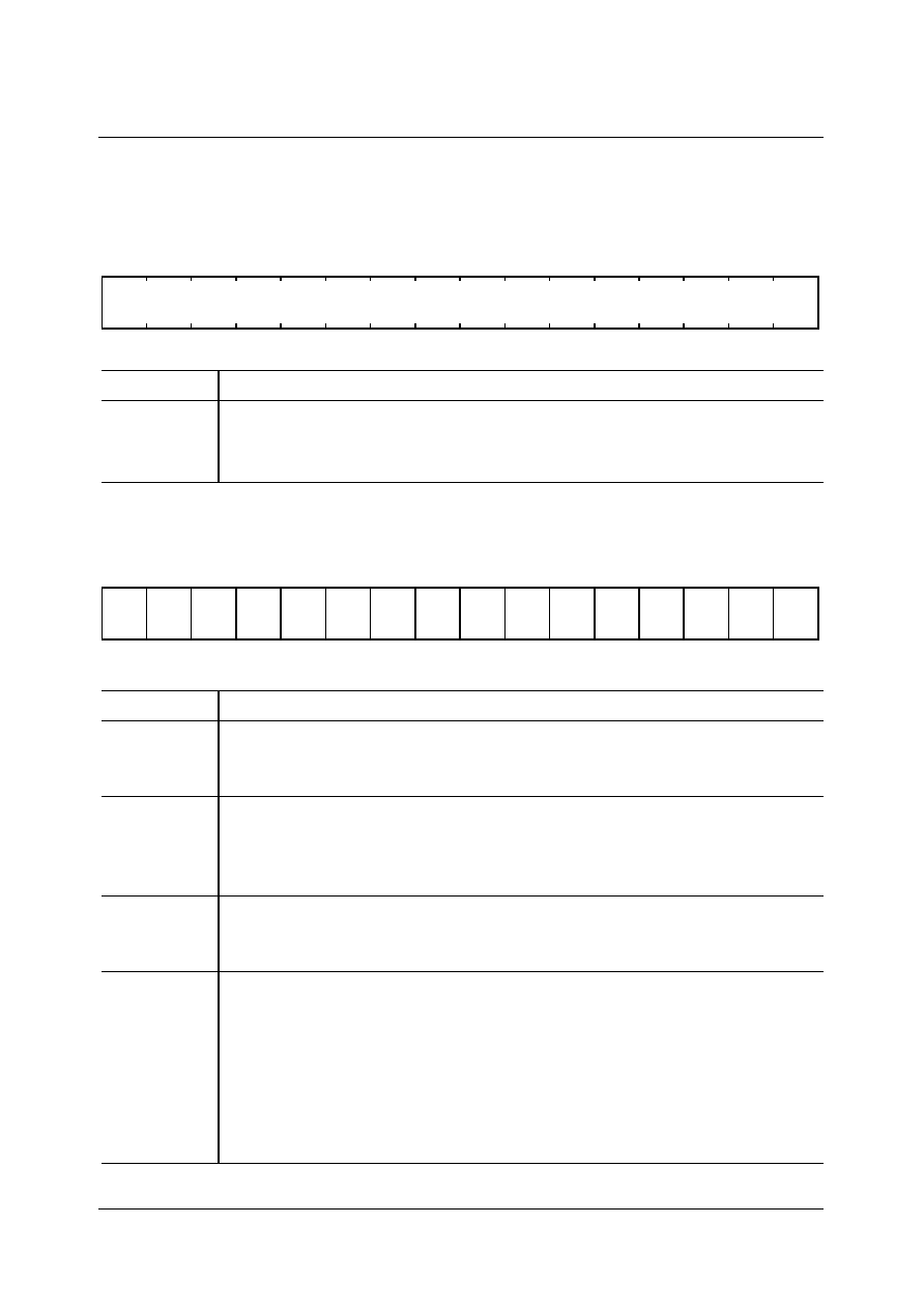
SDA 6000 / SDA 6001
PRELIMINARY DATA SHEET
Version 3.00
Slicer and Acquisition
12 - 22
Micronas
ACQFP8
Reset Value: XXXX
H
ACQFP9
Reset Value: XXXX
H
Bit
Function
WSS2_
DATA
(15 ... 0)
16 bits of sliced data of slicer 2 (WWS2_DATA(0) = last received bit)
(written to memory by ACQ-interface).
Note: See also ACQFP3 to ACQFP7
Bit
Function
STAB1
(status bit)
0:
H-PLL of slicer 1 not locked
1:
H-PLL of slicer 1 locked
(Written to memory by ACQ-interface)
VOK1
(status bit)
Vertical sync watchdog of slicer 1
0:
V-sync of slicer 1 not stable
1:
V-sync of slicer 1 stable
(Written to memory by ACQ-interface)
FIELD1
(status bit)
0:
Actual field of slicer 1 is field 1
1:
Actual field of slicer 1 is field 2
(Written to memory by ACQ-interface)
FREATTF
(status bit)
Frequency depending attenuation measurement (Field indicator)
High frequency CVBS1components (around 3.5 MHz) are strongly
damped (6 to 9 dB) compared to lower frequency CVBS1 components
0:
no frequency depending attenuation has been detected during the
last field
1:
for at least one text line during the last field frequency depending
attenuation has been detected.
(Written to memory by ACQ-interface)
5
4
3
2
1
0
11
10
9
8
7
6
15
14
13
12
WSS2_DATA(15..0)
5
4
3
2
1
0
11
10
9
8
7
6
15
14
13
12
0
0
0
STAB
1
0
0
VOK
1
FIELD
1
FREA
TTF
NOIS
E(1)
NOIS
E(0)
STAB
2
GRD
ON
GRD
SIGN
VOK
2
FIELD
2

SDA 6000 / SDA 6001
PRELIMINARY DATA SHEET
Version 3.00
Slicer and Acquisition
12 - 23
Micronas
ACQFP10
Reset Value: XXXX
H
NOISE
(1 ... 0)
(status bit)
Noise and co-channel detector of slicer 1
00: No noise and no co-channel-distortion has been detected.
01: No noise but co-channel-distortion has been detected.
10: Noise but no co-channel-distortion has been detected.
11:
Strong noise has been detected.
(Written to memory by ACQ-interface)
GRDON
(status bit)
Group delay detector of slicer 1
0:
No group delay distortion detected
1:
Group delay distortion detected
(Written to memory by ACQ-interface)
GRDSIGN
(status bit)
0:
If group delay distortion has been detected it was positive
1:
If group delay distortion has been detected it was negative
(Written to memory by ACQ-interface, CVBS input of slicer 1 is used)
STAB2
(status bit)
0:
H-PLL of slicer 2 not locked
1:
H-PLL of slicer 2 locked
(Written to memory by ACQ-interface)
VOK2
(status bit)
Vertical sync watchdog of slicer 2
0:
V-sync of slicer 2 not stable
1:
V-sync of slicer 2 stable
(Written to memory by ACQ-interface)
FIELD2
(status bit)
0:
Actual field of slicer 2 is field 1
1:
Actual field of slicer 2 is field 2
(Written to memory by ACQ-interface)
Bit
Function
LEOFLI
(11 ... 0)
This value is the output of the filter of the H-PLL of slicer 1 and
represents the actual horizontal period of CVBS1 in 33.33 MHz clock
cycles. This information can be used to measure the actual line
frequency of the CVBS signal.
Bit
Function
5
4
3
2
1
0
11
10
9
8
7
6
15
14
13
12
0
0
0
0
LEOFL(11.0)
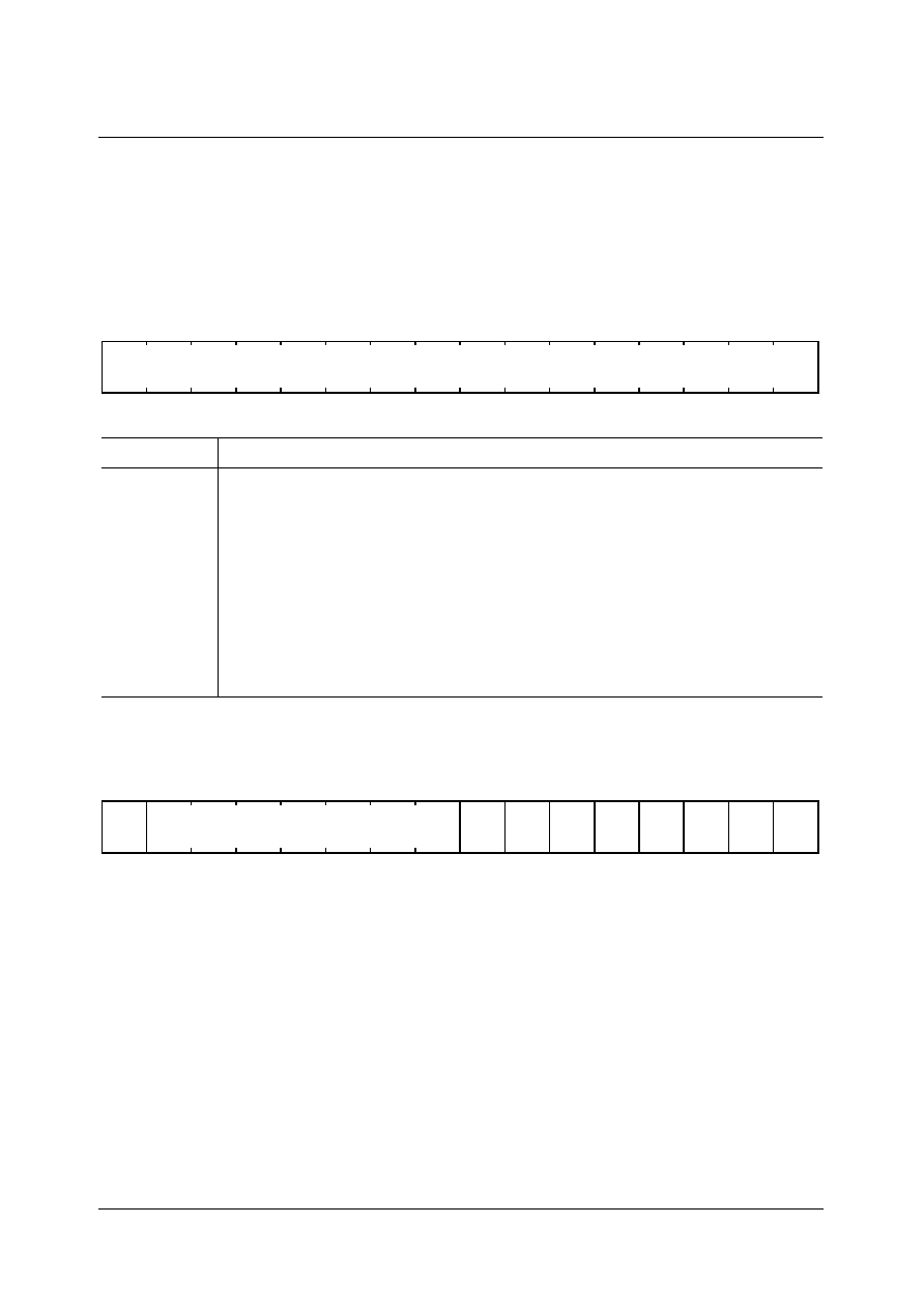
SDA 6000 / SDA 6001
PRELIMINARY DATA SHEET
Version 3.00
Slicer and Acquisition
12 - 24
Micronas
Line Parameters
Note: Line parameters only work on slicer 1 and have no influence on slicer 2.
ACQLP0
Reset Value: XXXX
H
ACQLP1
Reset Value: XXXX
H
Bit
Function
DINCR
(15 ... 0)
Specifies the frequency of the D-PLL of slicer 1. This parameter is used
to configure the D-PLL output frequency according to the service used.
DINCR =
f
data
�
2
18
/ 33.33 MHz
f
data
[MHz]
DINCR
6.9375
54559
5.7273
45041
5.0
39321
1.006993
7920
5
4
3
2
1
0
11
10
9
8
7
6
15
14
13
12
DINCR(15..0)
5
4
3
2
1
0
11
10
9
8
7
6
15
14
13
12
0
S1_DATA_STL
ACCU
ON
PLLT
ON
LOWP
ON
GDNO
N
PFIL
ON
GDPO
N
FRE
ON
NOI
ON

SDA 6000 / SDA 6001
PRELIMINARY DATA SHEET
Version 3.00
Slicer and Acquisition
12 - 25
Micronas
Bit
Function
S1_DATA_
STL
(6 ... 0)
Data start level, slicer 1
The value is used as threshold for the data-start-comparator of slicer1 if
S1_dstl_sel =1. Useful values are between black and maximum of
data.
This parameter takes effect only if EN_DATA_STL = 1.
ACCUON
Accumulator on
Improves slicing level calculation under noisy conditions.
If noise has been detected during automatic mode or if the bit NOION
has been set the internal slicing level calculation can be improved by
setting this bit.
0:
Standard slicing level calculation
1:
Improved slicing level calculation (improvement depends also on
parameter ALENGTH)
PLLLON
PLL tune on
If noise has been detected during automatic mode or if the bit NOION
has been set the data clock recovery PLL can be tuned throughout the
line by setting this bit.
0:
PLL is frozen after clock run in
1:
PLL is tuned throughout the line
LOWPON
Low Pass On
If noise has been detected during automatic mode or if the bit NOION
has been set a special low pass can be switched into the signal pass by
setting this bit (useful if mainly high frequency noise above 3.5 MHz is
present).
0:
Low pass is not used
1:
Low pass is used
PFILLON
Pre Filter On
If noise has been detected during automatic mode or if the bit NOION
has been set a second filter can be switched into the signal pass by
setting this bit (also useful if mainly high frequency noise above 3.5 MHz
is present).
0:
Low pass is not used.
1:
Low pass is used.
GDPON
0: Group
delay
compensation depends on AGDON
1:
Positive group delay compensation is always on
GDNON
0:
Group delay compensation depends on AGDON
1:
Negative group delay compensation is always on

SDA 6000 / SDA 6001
PRELIMINARY DATA SHEET
Version 3.00
Slicer and Acquisition
12 - 26
Micronas
ACQLP2
Reset Value: XXXX
H
FREON
0:
Frequency depending attenuation compensation depends on
AFRON
1:
Frequency depending attenuation compensation is always on
NOION
0:
Noise compensation depends on ANOON
1:
Noise compensation is always on
Bit
Function
FC1ER
Error tolerance of FC1 check
0:
No error allowed
1:
One error allowed
MLENGTH
(2 ... 0)
For noise suppression reasons a median filter has been introduced after
the actual data separation because of oversampling successive samples
could be averaged. Therefore an odd number of sliced successive
samples is taken and if the majority are `1' a `1' is sliced otherwise a `0'.
MLENGTH specifies how many samples are taken.
MLENGTH
Number of samples
000
1
001
3
010
5
011
7
100
9
101
11
110
13
111
15
Bit
Function
5
4
3
2
1
0
11
10
9
8
7
6
15
14
13
12
FC1
ER
MLENGTH(2..0)
ALENGTH
(1..0)
FCSEL(1..0)
CLKDIV(2..0)
NORM(2..0)
VCR
0

SDA 6000 / SDA 6001
PRELIMINARY DATA SHEET
Version 3.00
Slicer and Acquisition
12 - 27
Micronas
ALENGTH
(1 ... 0)
If noise has been detected or if NOISEON = 1, the output of the slicing
level filter is further averaged by means of an accumulation (arithmetic
averaging). ALENGTH specifies the number of slicing level filter output
values used for averaging. The accumulation clock depends on CLKDIV.
ALENGTH
Number of Slicing Level Output Values
used for Averaging
00
2
01
4
10
8
11
16
CLKDIV
The slicing level filter needs to find the DC value of the CVBS during CRI.
In order to do this it should suppress at least the CRI frequency. As
different services use different data frequencies the CRI frequency will
be different as well. Therefore the filter characteristic needs to be shifted.
This can be done by using different clocks for the filter. The filter itself
shows sufficient suppression for frequencies between 0.0757
�
SL
CLK
and 0.13
�
SL
CLK
(SL
CLK
is the actual filter clock and corresponds to
slicer 1)
CLKDIV
SL
CLK
000
1
�
f
s
001
1/2
�
f
s
010
1/3
�
f
s
011
1/4
�
f
s
100
1/5
�
f
s
101
1/6
�
f
s
110
1/7
�
f
s
111
1/8
�
f
s
Note:
f
s
= 33.33 MHz
NORM
Most timing signals are closely related to the actual data service used.
Therefore 3 bits specify the service received in the actual line.
NORM
Service
000
TXT
001
NABTS
010
VPS
011
WSS
100
CC
101
G+
110
reserved
111
US-WSS
Bit
Function
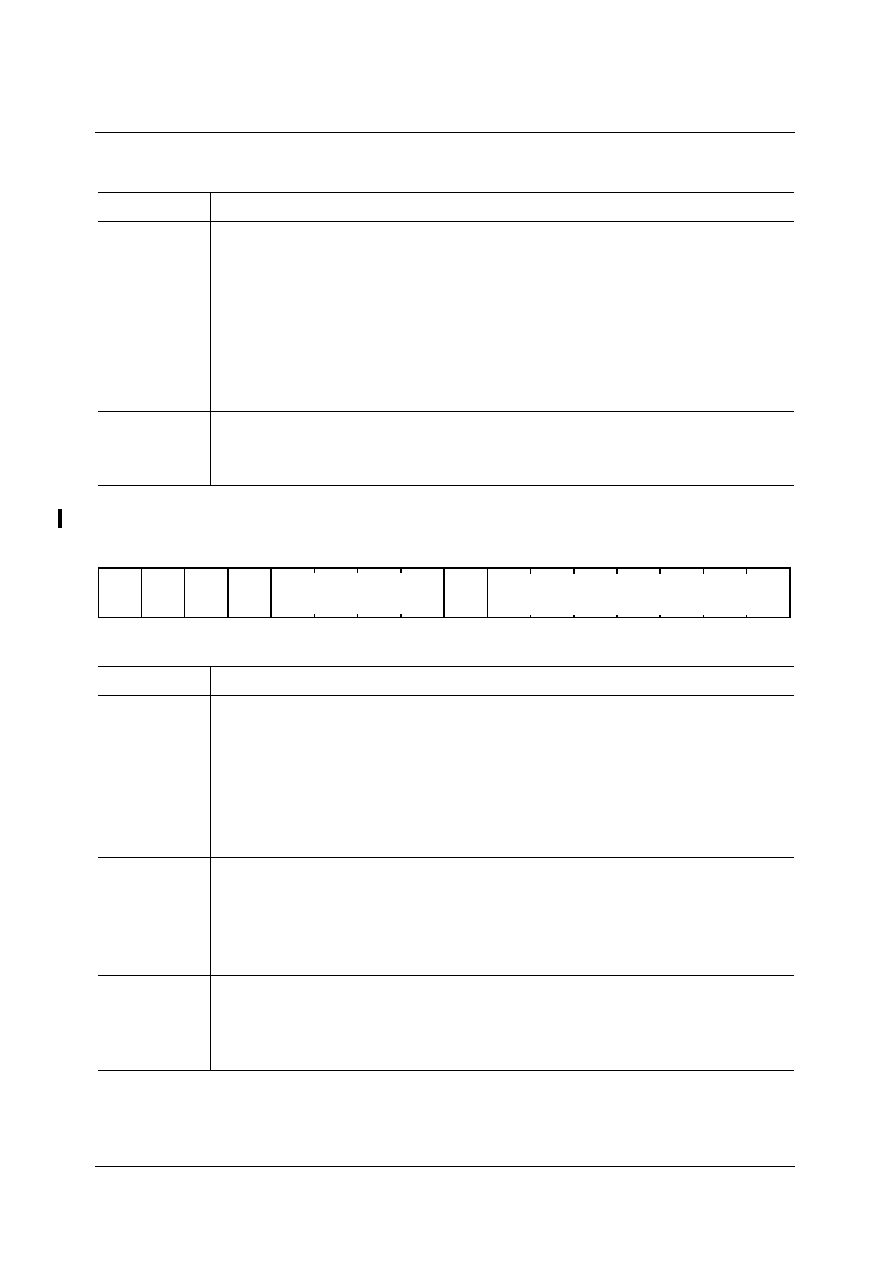
SDA 6000 / SDA 6001
PRELIMINARY DATA SHEET
Version 3.00
Slicer and Acquisition
12 - 28
Micronas
ACQLP3
Reset Value: XXXX
H
FCSEL
There are three different framing codes which can be used for each field.
The framing code used for the actual line is selected with FCSEL
(corresponds to slicer 1).
FCSEL
FC
00
FC1
01
FC2
10
FC3
11
No FC-check (all data are dumped to the VBI buffer)
VCR
This bit is used to change the behavior of the D-PLL and H-PLL.
0:
D-PLL tuning is stopped after CRI; H-PLL -> slow time constant
1:
D-PLL is tuned throughout the line; H-PLL -> fast time constant
Bit
Function
GD_COMP
(3 ... 0)
Group delay compensation
0000: small group delay can be compensated
.
.
.
0000: strong group delay can be compensated
This parameter takes effect only if EN_GD_COMP = 1.
SLSS
Slicing Level Source Selector
The slicer allows the use of an internal calculated slicing level or an
external set slicing level.
0:
Internal calculated slicing level is used.
1:
External set slicing level is used.
SSL(6 ... 0)
Set Slicing Level
If the bit SLSS is set the slicer is using the value of SSL as slicing level
instead of the internal calculated slicing level. The slicing level output in
parameter MSL is never the less the internal calculated value.
Bit
Function
5
4
3
2
1
0
11
10
9
8
7
6
15
14
13
12
GD_COMP
SLSS
SSL(6..0)

SDA 6000 / SDA 6001
PRELIMINARY DATA SHEET
Version 3.00
Slicer and Acquisition
12 - 29
Micronas
ACQLP4
Reset Value: XXXX
H
Bit
Function
FREATTL
Frequency Depending Attenuation Measurement (Line indicator)
High frequency-CVBS1-components (around 3.5 MHz) are strongly
damped (6 to 9 dB) compared to lower frequency-CVBS1-components
0:
no frequency depending attenuation has been detected for the
following line
1:
strong frequency depending attenuation has been detected for the
following line
(Written to memory by ACQ-interface)
MSL(6 ... 0) Measured Slicing Level
The value represents the slicing level which has been measured for the
current data line. The value can be used to calculate a better slicing level
especially for noisy signals by means of software averaging algorithms.
The improved slicing level can be set for the following fields by writing to
parameter SSL.
PERRP
(5 ... 0)
Phase Error Watch Dog Preliminary
(detection of test line CCIR331a or b)
The value shows how often in a line the internal PLL found strong phase
deviations between PLL and sliced data. The value can be used to detect
test line CCIR331a or b. This value is only preliminary as an exact result
is only available at the end of each line. For the exact value see PERR
at ACQLP5.
PERRP < 32? No test line.
PERRP > 31? Test line CCIR331a or b detected
TLDE
Test Line Detected (CCIR17 or CCIR18 or CCIR330)
0:
No test line of the above mentioned test lines has been detected
1:
The following data has most likely be sliced from a test line and
should therefor be ignored.
FCOK
Framing Code Received
0:
No framing code has been detected (no new data has been written
to memory)
1:
The selected framing code has been detected (new data has been
written to memory
5
4
3
2
1
0
11
10
9
8
7
6
15
14
13
12
FREA
TTL
MSL(6..0)
PERRP(5..0)
TLDE FCOK

SDA 6000 / SDA 6001
PRELIMINARY DATA SHEET
Version 3.00
Slicer and Acquisition
12 - 30
Micronas
ACQLP5
Reset Value: XXXX
H
Bit
Function
BLACK
(6 ... 0)
Measured black level of slicer 1
PERR
(5 ... 0)
Phase Error Watch Dog
(detection of test line CCIR331a or b)
This is the exact phase error watch dog output for the current line. The
value shows how often in a line the internal PLL found strong phase
deviations between PLL and sliced data. The value can be used to detect
test line CCIR331a or b.
PERR < 32? No test line.
PERR > 31? Test line CCIR331a or b detected
5
4
3
2
1
0
11
10
9
8
7
6
15
14
13
12
0
0
0
BLACK
PERR(5..0)

SDA 6000 / SDA 6001
PRELIMINARY DATA SHEET
Version 3.00
Slicer and Acquisition
12 - 31
Micronas
12.5.2
Recommended Parameter Settings
TTX
VPS
WSS
CC
G+
AGDON
1
0
0
0
0
AFRON
1
0
0
0
0
ANOON
1
1
1
1
1
GDPON
0
0
0
0
0
GDNON
0
0
0
0
0
FREON
0
0
0
0
0
PFILON
0
1
1
1
1
LOWPON
0
1
1
1
1
PLLTON
0
1
1
1
1
ACCUON
0
1
1
1
1
NOION
0
0
0
0
0
FULL
0
0
0
0
0
DINCR
54559
45041
39321
7864
7920
FC1ER
0
0
0
0
0
MLENGTH
1
2
7
7
7
ALENGTH
2
2
2
2
2
CLKDIV
0
0
2
5
5
NORM
0
2
3
4
5
FCSEL
0
1
2
2
2
VCR
0
0
0
0
0
FC1
228
don't care
don't care
don't care
don't care
FC3
don't care
don't care
don't care
3
1261
FC3MASK
don't care
don't care
don't care
65472
63488

Register Overview

SDA 6000 / SDA 6001
PRELIMINARY DATA SHEET
Version 3.00
Register Overview
13 - 3
Micronas
13
Register Overview
This section summarizes all SFR and ESFR registers, which are implemented in M2 and
explains the description format which is used in the previous chapters to describe the
functionality of the SFRs. Display generators and slicers are mainly programmed via
RAM registers which are not mentioned in this chapter, due to their variable position in
the RAM. RAM registers are principally undefined after reset.
For easy reference the registers are ordered according to two different keys:
� Ordered by their functional context
� Ordered by register address, to find the location of a specific register.
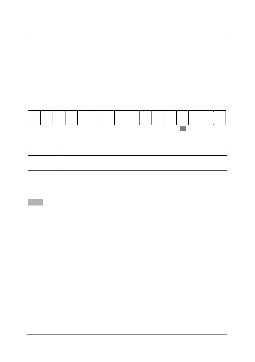
SDA 6000 / SDA 6001
PRELIMINARY DATA SHEET
Version 3.00
Register Overview
13 - 4
Micronas
13.1
Register Description Format
In the respective chapters the function and the layout of the SFRs is described in a
specific format which provides a number of details about the described special function
register. The example below shows how to interpret these details.
A register looks like this:
REG_NAME
Reset Value: ****
H
REG_NAME Name of this register.
* * * *
Register contents after reset.
0/1: defined value, `X': undefined after power up.
Bits that are set/cleared by hardware are marked with a shaded access
box.
r
Read only register.
rw
Register can be read and written.
-
Reserved register bit. Reading such bits delivers an undefined value. If
such a bit is written then only `0' is allowed.
Bit
Function
bit(field)
name
Explanation of bit(field)name
Description of the functions controlled by this bit(field).
5
4
3
2
1
0
11
10
9
8
7
6
15
14
13
12
w
r
rw
rw
rw
-
-
-
-
-
-
-
-
-
write
only
read
only
std
bit
hw
bit
bitfield(2:0)
rw

SDA 6000 / SDA 6001
PRELIMINARY DATA SHEET
Version 3.00
Register Overview
13 - 5
Micronas
13.2
CPU General Purpose Registers (GPRs)
The GPRs form the register bank with which the CPU works. This register bank may be
located anywhere within the internal RAM via the Context Pointer (CP). Due to the
addressing mechanism, GPR banks can only reside within the internal RAM. All GPRs
are bit-addressable.
The first 8 GPRs (R7 ... R0) may also be accessed via the byte. Other than with SFRs,
writing to a GPR byte does not affect the other byte of the respective GPR.
The respective half of the byte-accessible registers receive special names:
Name
Physical
Address
8-Bit
Address
Description
Reset
Value
R0
(CP) + 0
F0
H
CPU General Purpose (Word) Register R0
XXXX
H
R1
(CP) + 2
F1
H
CPU General Purpose (Word) Register R1
XXXX
H
R2
(CP) + 4
F2
H
CPU General Purpose (Word) Register R2
XXXX
H
R3
(CP) + 6
F3
H
CPU General Purpose (Word) Register R3
XXXX
H
R4
(CP) + 8
F4
H
CPU General Purpose (Word) Register R4
XXXX
H
R5
(CP) + 10 F5
H
CPU General Purpose (Word) Register R5
XXXX
H
R6
(CP) + 12 F6
H
CPU General Purpose (Word) Register R6
XXXX
H
R7
(CP) + 14 F7
H
CPU General Purpose (Word) Register R7
XXXX
H
R8
(CP) + 16 F8
H
CPU General Purpose (Word) Register R8
XXXX
H
R9
(CP) + 18 F9
H
CPU General Purpose (Word) Register R9
XXXX
H
R10
(CP) + 20 FA
H
CPU General Purpose (Word) Register R10
XXXX
H
R11
(CP) + 22 FB
H
CPU General Purpose (Word) Register R11
XXXX
H
R12
(CP) + 24 FC
H
CPU General Purpose (Word) Register R12
XXXX
H
R13
(CP) + 26 FD
H
CPU General Purpose (Word) Register R13
XXXX
H
R14
(CP) + 28 FE
H
CPU General Purpose (Word) Register R14
XXXX
H
R15
(CP) + 30 FF
H
CPU General Purpose (Word) Register R15
XXXX
H

SDA 6000 / SDA 6001
PRELIMINARY DATA SHEET
Version 3.00
Register Overview
13 - 6
Micronas
Name
Physical
Address
8-Bit
Address
Description
Reset
Value
RL0
(CP) + 0
F0
H
CPU General Purpose (Byte) Register RL0
XX
H
RH0
(CP) + 1
F1
H
CPU General Purpose (Byte) Register RH0
XX
H
RL1
(CP) + 2
F2
H
CPU General Purpose (Byte) Register RL1
XX
H
RH1
(CP) + 3
F3
H
CPU General Purpose (Byte) Register RH1
XX
H
RL2
(CP) + 4
F4
H
CPU General Purpose (Byte) Register RL2
XX
H
RH2
(CP) + 5
F5
H
CPU General Purpose (Byte) Register RH2
XX
H
RL3
(CP) + 6
F6
H
CPU General Purpose (Byte) Register RL3
XX
H
RH3
(CP) + 7
F7
H
CPU General Purpose (Byte) Register RH3
XX
H
RL4
(CP) + 8
F8
H
CPU General Purpose (Byte) Register RL4
XX
H
RH4
(CP) + 9
F9
H
CPU General Purpose (Byte) Register RH4
XX
H
RL5
(CP) + 10 FA
H
CPU General Purpose (Byte) Register RL5
XX
H
RH5
(CP) + 11 FB
H
CPU General Purpose (Byte) Register RH5
XX
H
RL6
(CP) + 12 FC
H
CPU General Purpose (Byte) Register RL6
XX
H
RH6
(CP) + 13 FD
H
CPU General Purpose (Byte) Register RH6
XX
H
RL7
(CP) + 14 FE
H
CPU General Purpose (Byte) Register RL7
XX
H
RH7
(CP) + 15 FF
H
CPU General Purpose (Byte) Register RH7
XX
H
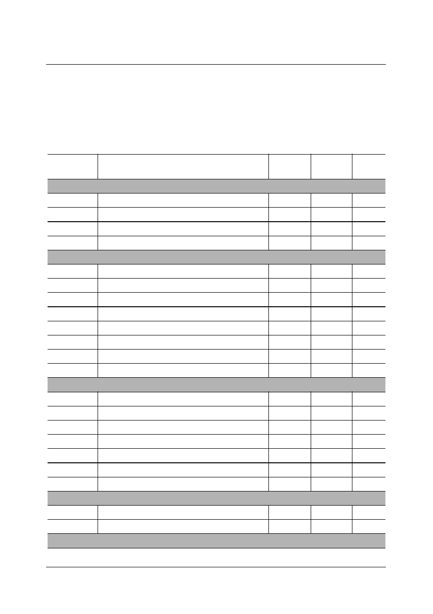
SDA 6000 / SDA 6001
PRELIMINARY DATA SHEET
Version 3.00
Register Overview
13 - 7
Micronas
13.3
Registers Ordered by Context
The following table lists all SFRs which are implemented in the M2 grouped by their
context. Their actual address can be seen in the next chapter.
Table 13-1
Name
Description
Physical
Address
8-Bit
Address
Reset
Value
SSC Registers
SSCCON
Control Register
FFB2
H
D9
H
0000
H
SSCBR
Baud Rate Timer Reload Register
F0B4
H
5A
H
0000
H
SSCTB
Transmit Buffer Register
F0B0
H
58
H
0000
H
SSCRB
Receive Buffer Register
F0B2
H
59
H
0000
H
ASC Registers
S0CON
Control Register
FFB0
H
D8
H
0000
H
S0ABSTAT Autobaud Status Register
F0B8
H
5C
H
0000
H
S0ABCON
Autobaud Control Register
F1B8
H
DC
H
0000
H
S0BG
Baud Rate Timer Reload Register
FEB4
H
5A
H
0000
H
S0FDV
Fractional Divider Register
FEB6
H
5B
H
0000
H
S0PMW
IrDA Pulse Mode and Width Register
FEAA
H
55
H
0000
H
S0TBUF
Transmit Buffer Register
FEB0
H
58
H
0000
H
S0RBUF
Receive Buffer Register
FEB2
H
59
H
0000
H
I
2
C Registers
ICCFG
2)
I
2
C Configuration Register
E810
H
-/-
0000
H
ICCON
2)
I
2
C Control Register
E812
H
-/-
0000
H
ICST
2)
I
2
C Status Register
E814
H
-/-
0000
H
ICADR
2)
I
2
C Address Register
E816
H
-/-
0000
H
ICRTBL
2)
I
2
C Receive/Transmit Buffer (Low Word)
E818
H
-/-
0000
H
ICRTBH
2)
I
2
C Receive/Transmit Buffer (High Word)
E81A
H
-/-
0000
H
IICPISEL
2)
I
2
C Port Input Selection Register
E804
H
-/-
0000
H
Watchdog Timer Registers
WDTCON
Control Register
FFAE
H
D7
H
000X
H
WDT
Timer Register
FEAE
H
57
H
0000
H
Realtime Clock Registers

SDA 6000 / SDA 6001
PRELIMINARY DATA SHEET
Version 3.00
Register Overview
13 - 8
Micronas
RTCCON
Control Register
F1CC
H
E6
H
0003
H
T14REL
Prescaler Timer Reload
F0D0
H
68
H
0000
H
T14
Prescaler Timer T14
F0D2
H
69
H
0000
H
RTCL
Count Register Low Word
F0D4
H
6A
H
0000
H
RTCH
Count Register High Word
F0D6
H
6B
H
0000
H
RTCRELL
Reload Register Low Word
F0CC
H
66
H
0000
H
RTCRELH
Reload Register High Word
F0CE
H
67
H
0000
H
RTCISNC
RTC Interrupt Subnode Control (1st Level) F1C8
H
E4
H
0000
H
ISNC
RTC Interrupt Subnode Control (2nd Level) F1DE
H
EF
H
0000
H
Table 13-1
(cont'd)
Name
Description
Physical
Address
8-Bit
Address
Reset
Value
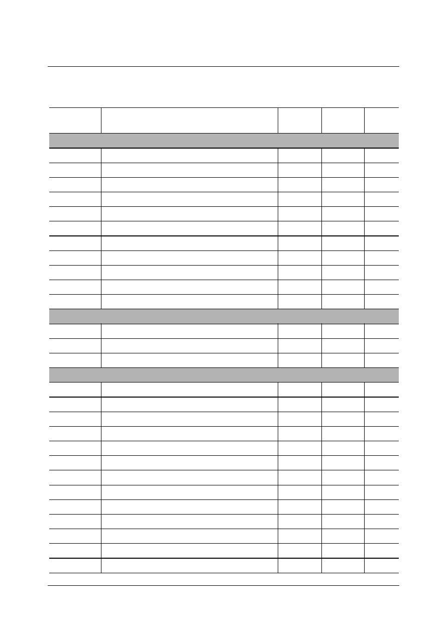
SDA 6000 / SDA 6001
PRELIMINARY DATA SHEET
Version 3.00
Register Overview
13 - 9
Micronas
General Purpose Timer Registers (GPT1/2)
T2CON
GPT1 Timer 2 Control Register
FF40
H
A0
H
0000
H
T3CON
GPT1 Timer 3 Control Register
FF42
H
A1
H
0000
H
T4CON
GPT1 Timer 4 Control Register
FF44
H
A2
H
0000
H
T5CON
GPT2 Timer 5 Control Register
FF46
H
A3
H
0000
H
T6CON
GPT2 Timer 6 Control Register
FF48
H
A4
H
0000
H
T2
GPT1 Timer 2 Register
FE40
H
20
H
0000
H
T3
GPT1 Timer 3 Register
FE42
H
21
H
0000
H
T4
GPT1 Timer 4 Register
FE44
H
22
H
0000
H
T5
GPT2 Timer 5 Register
FE46
H
23
H
0000
H
T6
GPT6 Timer 2 Register
FE48
H
24
H
0000
H
CAPREL
GPT1 Capture Reload Register
FE4A
H
25
H
0000
H
ADC Registers
ADDAT1
ADC Data Register for Channel 1 and 2
FEA0
H
50
H
0000
H
ADDAT2
ADC Data Register for Channel 3 and 4
FEA2
H
51
H
0000
H
ADCCON
ADC Control Register
FEA4
H
52
H
0000
H
Interrupt Control Registers
T2IC
Timer 2 Interrupt Control Register
FF60
H
B0
H
0000
H
T3IC
Timer 3 Interrupt Control Register
FF62
H
B1
H
0000
H
T4IC
Timer 4 Interrupt Control Register
FF64
H
B2
H
0000
H
T5IC
Timer 5 Interrupt Control Register
FF66
H
B3
H
0000
H
T6IC
Timer 6 Interrupt Control Register
FF68
H
B4
H
0000
H
CRIC
CAPREL Interrupt Control Register
FF6A
H
B5
H
0000
H
EX0IC
External Interrupt Control Register 0
FF88
H
C4
H
0000
H
EX1IC
External Interrupt Control Register 1
FF8A
H
C5
H
0000
H
EX2IC
External Interrupt Control Register 2
FF8C
H
C6
H
0000
H
EX3IC
External Interrupt Control Register 3
FF8E
H
C7
H
0000
H
EX4IC
External Interrupt Control Register 4
FF90
H
C8
H
0000
H
EX5IC
External Interrupt Control Register 5
FF92
H
C9
H
0000
H
EX6IC
External Interrupt Control Register 6
FF94
H
CA
H
0000
H
Table 13-1
(cont'd)
Name
Description
Physical
Address
8-Bit
Address
Reset
Value

SDA 6000 / SDA 6001
PRELIMINARY DATA SHEET
Version 3.00
Register Overview
13 - 10
Micronas
EX7IC
External Interrupt Control Register 7
FF96
H
CB
H
0000
H
ADC1IC
A/D Conversion Interrupt Control
(Channel 1 + 2)
FF98
H
CC
H
0000
H
ADC2IC
A/D Conversion Interrupt Control
(Channel 3 + 4)
FF9A
H
CD
H
0000
H
ADWIC
A/D Wake Up Interrupt
F178
H
BC
H
0000
H
SSCEIC
SSC Error Interrupt Control
FF76
H
BB
H
0000
H
SSCRIC
SSC Receive Interrupt Control
FF74
H
BA
H
0000
H
SSCTIC
SSC Transmit Interrupt Control
FF72
H
B9
H
0000
H
S0EIC
ASC Error Interrupt Control
FF70
H
B8
H
0000
H
S0RIC
ASC Receive Interrupt Control
FF6E
H
B7
H
0000
H
S0TIC
ASC Transmit Interrupt Control
FF6C
H
B6
H
0000
H
S0TBIC
ASC Transmit Buffer Interrupt Control
F19C
H
CE
H
0000
H
ABSTOIC
ASC Autobaud Stop Interrupt Control
F17A
H
BD
H
0000
H
ABSTAIC
ASC Autobaud Start Interrupt Control
FF9E
H
CF
H
0000
H
I
2
CTIC
I
2
C Transfer Interrupt Control
F194
H
CA
H
0000
H
I
2
CPIC
I
2
C Protocol Interrupt Control
F18C
H
C6
H
0000
H
I
2
CTEIC
I
2
C Transmission End Interrupt Control
F184
H
C2
H
0000
H
ACQIC
Acquisition-Interrupt Control
F176
H
BB
H
0000
H
VSDISIC
Display-Vertical-Sync Interrupt Control
F174
H
BA
H
0000
H
HSDISIC
Display-Horizontal-Sync Interrupt Control
F172
H
B9
H
0000
H
GAFIC
Graphic Accelerator Interrupt Control
FF9C
H
CE
H
0000
H
RTCIC
Realtime Clock Interrupt Control
F19E
H
CF
H
0000
H
PECCLIC
PEC Link Interrupt Control
F180
H
C0
H
0000
H
PEC Interrupt Control Registers
PECC0
PEC Channel 0 Control Register
FEC0
H
60
H
0000
H
PECC1
PEC Channel 1 Control Register
FEC2
H
61
H
0000
H
PECC2
PEC Channel 2 Control Register
FEC4
H
62
H
0000
H
PECC3
PEC Channel 3 Control Register
FEC6
H
63
H
0000
H
PECC4
PEC Channel 4 Control Register
FEC8
H
64
H
0000
H
Table 13-1
(cont'd)
Name
Description
Physical
Address
8-Bit
Address
Reset
Value
SDA 6000 / SDA 6001
PRELIMINARY DATA SHEET
Version 3.00
Register Overview
13 - 11
Micronas
PECC5
PEC Channel 5 Control Register
FECA
H
65
H
0000
H
PECC6
PEC Channel 6 Control Register
FECC
H
66
H
0000
H
PECC7
PEC Channel 7 Control Register
FECE
H
67
H
0000
H
PECSN0
PEC Segment Number Channel 0 Register FED0
H
68
H
0000
H
PECSN1
PEC Segment Number Channel 1 Register FED2
H
69
H
0000
H
PECSN2
PEC Segment Number Channel 2 Register FED4
H
6A
H
0000
H
PECSN3
PEC Segment Number Channel 3 Register FED6
H
6B
H
0000
H
PECSN4
PEC Segment Number Channel 4 Register FED8
H
6C
H
0000
H
PECSN5
PEC Segment Number Channel 5 Register FEDA
H
6D
H
0000
H
PECSN6
PEC Segment Number Channel 6 Register FEDC
H
6E
H
0000
H
PECSN7
PEC Segment Number Channel 7 Register FEDE
H
6F
H
0000
H
CLISNC
PEC Channel Link Interrupt Subnode
Register
FFA8
H
D4
H
0000
H
Port Registers
RP0H
Reset Configuration at Port 4 (read only)
F108
H
85
H
XX
H
P2
Port 2 Register
FFC0
H
E0
H
0000
H
P3
Port 3 Register
FFC4
H
E2
H
0000
H
P4
Port 4 Register
FFC8
H
E4
H
0000
H
P5
Port 5 Register
FFA2
H
D1
H
0000
H
P6
Port 6 Register
FFCC
H
E6
H
0000
H
DP2
Direction Control Register Port 2
FFC2
H
E1
H
0000
H
DP3
Direction Control Register Port 3
FFC6
H
E3
H
0000
H
DP6
Direction Control Register Port 6
FFCE
H
E7
H
0000
H
ODP3
Open Drain Control Register Port 3
F1C6
H
E3
H
0000
H
ODP6
Open Drain Control Register Port 6
F1CE
H
E7
H
0000
H
P5BEN
Analog/Digital Input Enable Register Port 5 F1C2
H
E1
H
0000
H
ALTSEL0P6 Alternate Function Enable Register Port 6 F12C
H
96
H
0000
H
Specific Control Registers
HSGL_WIN Slicer Control Register
FF4C
H
A6
H
0000
H
Table 13-1
(cont'd)
Name
Description
Physical
Address
8-Bit
Address
Reset
Value

SDA 6000 / SDA 6001
PRELIMINARY DATA SHEET
Version 3.00
Register Overview
13 - 12
Micronas
EN_ACQ_P
ARAM
Slicer Control Register
FF4A
H
A5
H
0000
H
STRVBI
VBI Buffer Start Register
F1A0
H
D0
H
0000
H
FSMOBSA
Registers for Micronas internal evaluation
of graphic-accelerator
Must be kept in reset state.
F020
H
10
H
0000
H
FRXCON
F026
H
13
H
0000
H
DGWDCON
F0C4
H
62
H
0000
H
DGWDSNT
F0C6
H
63
H
0000
H
TOXDGI
F120
H
90
H
FFFF
H
TOXGAA
F122
H
91
H
FFFF
H
TOXGAB
F124
H
92
H
FFFF
H
TOXSRU
F126
H
93
H
FFFF
H
AMIWDCON
F128
H
94
H
0000
H
AMIWDSNT
F12A
H
95
H
0000
H
TOXAMI
F130
H
98
H
FFFF
H
TOXICACHE
F132
H
99
H
FFFF
H
TOXDCACHE
F134
H
9A
H
FFFF
H
TOXACI
F136
H
9B
H
FFFF
H
FRXDGI
F140
H
A0
H
0000
H
FRXGAA
F142
H
A1
H
0000
H
FRXGAB
F144
H
A2
H
0000
H
FRXSRU
F146
H
A3
H
0000
H
FRXAMI
F150
H
A8
H
0000
H
FRXICACHE
F152
H
A9
H
0000
H
FRXDCACHE
F154
H
AA
H
0000
H
FRXACI
F156
H
AB
H
0000
H
DGFSM
FE38
H
1C
H
xxxx
H
DGXTF
FE3A
H
1D
H
xxxx
H
AMIFSM
FE58
H
2C
H
xxxx
H
AMIXTF
FE5A
H
2D
H
xxxx
H
Table 13-1
(cont'd)
Name
Description
Physical
Address
8-Bit
Address
Reset
Value
SDA 6000 / SDA 6001
PRELIMINARY DATA SHEET
Version 3.00
Register Overview
13 - 13
Micronas
PXDEL
Pixel Delay Register
F198
H
CC
H
0000
H
ACQISN
Acquisition Interrupt Subnode Register
F1A2
H
D1
H
0000
H
GPRGCRL GAI Instruction Start Register (Low Word) F1A4
H
D2
H
0000
H
GPRGCRH GAI Instruction Start Register (High Word) F1A6
H
D3
H
0000
H
DGCON
Display Generator Control
FEFA
H
7D
H
0000
H
SCR
Sync Control Register
F1A8
H
D4
H
0000
H
SCR2
Sync Control Register2
F148
H
A4
H
0011
H
VLR
Vertical Line Register
F1AA
H
D5
H
0271
H
BVCR
Begin of Vertical Clamping
FEF6
H
7B
H
0001
H
EVCR
End of Vertical Clamping
FEF8
H
7C
H
0005
H
HPR
Horizontal Period Register
F1AC
H
D6
H
0855
H
SDV
Vertical Sync Delay Register
F1AE
H
D7
H
0020
H
SDH
Horizontal Sync Delay Register
F1B0
H
D8
H
0020
H
HCR
Horizontal Clamping Register
F1B2
H
D9
H
1400
H
PFR
Pixel Frequency Register
F1B6
H
DB
H
00A4
H
DACCON
RGB - DAC Control Register
F1B4
H
DA
H
0005
H
RGBINTFC_EN
Digital RGB Interface Enable
F0A0
H
50
H
0000
H
CLKINTFC_EN
External Pixel Clock Enable
F0A2
H
51
H
0000
H
External Bus Interface Control Registers
REDIR
Memory Map Redirection Register
F1BA
H
DD
H
0000
H
REDIR1
Memory Map Redirection Register 1
F1CA
H
E5
H
00FF
H
EBICON
Control Register for EBI
F1BC
H
DE
H
0000
H
EBIDIR
Direct Access Register for EBI
F1BE
H
DF
H
0000
H
EBIREF
SDRAM Auto Refresh Cycle Control
F100
H
80
H
03E8
H
OCDS Registers
COMDATA Communication Mode Data Register
F068
H
34
H
0000
H
RWDATA
Read/Write Mode Data Register
F06A
H
35
H
0000
H
IOSR
Communication Mode Status Register
F06C
H
36
H
0000
H
DCMPLL
Hardware Trigger Range Comparison
Lower Bound
F0DC
H
6E
H
0000
H
1)
Table 13-1
(cont'd)
Name
Description
Physical
Address
8-Bit
Address
Reset
Value
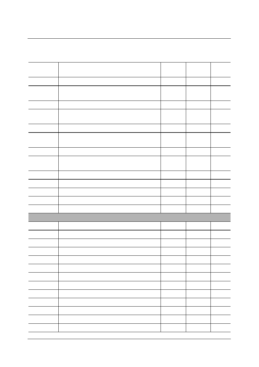
SDA 6000 / SDA 6001
PRELIMINARY DATA SHEET
Version 3.00
Register Overview
13 - 14
Micronas
DCMPLH
Extension of Register DCMPLL
F0DE
H
6F
H
0000
H
1)
DCMPGL
Hardware Trigger Range Comparison
Upper Bound
F0E0
H
70
H
0000
H
1)
DCMPGH
Extension of Register DCMPGL
F0E2
H
71
H
0000
H
1)
DCMP0L
Hardware Trigger Equal Comparison
Register 0
F0E4
H
72
H
0000
H
1)
DCMP0H
Extension of Register DCMP0L
F0E6
H
73
H
0000
H
1)
DCMP1L
Hardware Trigger Equal Comparison
Register 1
F0E8
H
74
H
0000
H
1)
DCMP1H
Extension of Register DCMP1L
F0EA
H
75
H
0000
H
1)
DCMP2L
Hardware Trigger Equal Comparison
Register 2
F0EC
H
76
H
0000
H
1)
DCMP2H
Extension of Register DCMP2L
F0EE
H
77
H
0000
H
1)
DTREVT
Hardware Trigger Event Control
F0F0
H
78
H
0000
H
1)
DSWEVT
Software Trigger Event Control
F0F4
H
7A
H
0000
H
1)
DEXEVT
External Trigger Event Control
F0F8
H
7C
H
0000
H
1)
DBGSR
Debug Status Register
F0FC
H
7E
H
0000
H
1)
System & CPU Registers
TFR
Trap Flag Register
FFAC
H
D6
H
0000
H
ADDRSEL1 Address Select Register 1
FE18
H
0C
H
0000
H
ADDRSEL2 Address Select Register 2
FE1A
H
0D
H
0000
H
ADDRSEL3 Address Select Register 3
FE1C
H
0E
H
0000
H
ADDRSEL4 Address Select Register 4
FE1E
H
0F
H
0000
H
BUSCON0
Bus Configuration Register 0
FF0C
H
86
H
0000
H
BUSCON1
Bus Configuration Register 1
FF14
H
8A
H
0000
H
BUSCON2
Bus Configuration Register 2
FF16
H
8B
H
0000
H
BUSCON3
Bus Configuration Register 3
FF18
H
8C
H
0000
H
BUSCON4
Bus Configuration Register 4
FF1A
H
8D
H
0000
H
SYSCON
CPU System Configuration Register
FF12
H
89
H
0400
H
SYSCON1
CPU System Configuration Register 1
F1DC
H
EE
H
0000
H
SYSCON2
CPU System Configuration Register 2
F1D0
H
E8
H
0000
H
Table 13-1
(cont'd)
Name
Description
Physical
Address
8-Bit
Address
Reset
Value

SDA 6000 / SDA 6001
PRELIMINARY DATA SHEET
Version 3.00
Register Overview
13 - 15
Micronas
XADRS1
External Address Select Register 1
F014
H
0A
H
0000
H
XADRS2
External Address Select Register 2
F016
H
0B
H
0000
H
XADRS3
External Address Select Register 3
F018
H
0C
H
0000
H
XADRS4
External Address Select Register 4
F01A
H
0D
H
0000
H
XADRS5
External Address Select Register 5
F01C
H
0E
H
0000
H
XADRS6
External Address Select Register 6
F01E
H
0F
H
0000
H
XBCON1
XBUS Control Register 1
F114
H
8A
H
0000
H
XBCON2
XBUS Control Register 2
F116
H
8B
H
0000
H
XBCON3
XBUS Control Register 3
F118
H
8C
H
0000
H
XBCON4
XBUS Control Register 4
F11A
H
8D
H
0000
H
XBCON5
XBUS Control Register 5
F11C
H
8E
H
0000
H
XBCON6
XBUS Control Register 6
F11E
H
8F
H
0000
H
DPP0
CPU Data Page Pointer 0 (10bits)
FE00
H
00
H
0000
H
DPP1
CPU Data Page Pointer 1 (10bits)
FE02
H
01
H
0001
H
DPP2
CPU Data Page Pointer 2 (10bits)
FE04
H
02
H
0002
H
DPP3
CPU Data Page Pointer 3 (10bits)
FE06
H
03
H
0003
H
MDH
CPU Multiply Divide Control Register High
Word
FE0C
H
06
H
0000
H
MDL
CPU Multiply Divide Control Register Low
Word
FE0E
H
07
H
0000
H
MDC
CPU Multiply Divide Control Register
FF0E
H
87
H
0000
H
PSW
CPU Program Status Word
FF10
H
88
H
0000
H
STKUN
CPU Stack Underflow Pointer Register
FE16
H
0B
H
0000
H
STKOV
CPU Stack Overflow Pointer Register
FE14
H
0A
H
0000
H
SP
CPU System Stack Pointer
FE12
H
09
H
FC00
H
CP
CPU Context Pointer
FE10
H
08
H
FC00
H
CSP
CPU Code Segment Control Register
FE08
H
04
H
0000
H
SCUSLC
Security Level Command Register
F0C0
H
60
H
0000
H
SCUSLS
Security Level Status Register
F0C2
H
61
H
0000
H
ZEROS
Constant Value 0's Register (read only)
FF1C
H
8E
H
0000
H
Table 13-1
(cont'd)
Name
Description
Physical
Address
8-Bit
Address
Reset
Value

SDA 6000 / SDA 6001
PRELIMINARY DATA SHEET
Version 3.00
Register Overview
13 - 16
Micronas
ONES
Constant Value 1's Register (read only)
FF1E
H
8F
H
FFFF
H
XPERCON X-Peripheral Control Register
F024
H
12
H
0000
H
EXISEL
Alternative External Interrupt Selection
F1DA
H
ED
H
0000
H
EXICON
External Interrupt Control
F1C0
H
E0
H
0000
H
OSCCON
Oscillator Pad Control Register
F1C4
H
E2
H
0001
H
IDMANUF
Manufacture ID
F07E
H
3F
H
XXXX
H
IDCHIP
Chip ID
F07C
H
3E
H
XXXX
H
CPUID
Identifies the core of CPU
F00C
H
06
H
0061
H
TM_LO
Hardware Testmode Register Low
FEFC
H
7E
H
0000
H
TM_HI
Hardware Testmode Register High
FEFE
H
7F
H
0000
H
FOCON
SCU Register (no Function within M2)
FFAA
H
D5
H
0000
H
SYSCON3
SCU Register (no Function within M2)
F1D4
H
EA
H
0000
H
1)
OCDS related registers that are not reset during a controller reset.
2)
No 8-bit addresses provided for XBUS registers.
Table 13-1
(cont'd)
Name
Description
Physical
Address
8-Bit
Address
Reset
Value

SDA 6000 / SDA 6001
PRELIMINARY DATA SHEET
Version 3.00
Register Overview
13 - 17
Micronas
13.4
Registers Ordered by Address
The following tables summarize the register symbols and their "short addresses". The
physical address can be calculated by multiplying the short address by 2 and adding that
value to FE00
H
for the SFR register area and adding F000
H
for the extended SFR area.
Bit-addressable registers are highlighted in gray.

SDA 6000 / SDA 6001
PRELIMINARY DATA SHEET
Version 3.00
Register Overview
13 - 18
Micronas
13.4.1
Registers in SFR Area
Address
+ 00
H
+ 01
H
+ 02
H
+ 03
H
+ 04
H
+ 05
H
+ 06
H
+ 07
H
00
H
DPP0
DPP1
DPP2
DPP3
CSP
reserved
MDH
MDL
08
H
CP
SP
STKOV
STKUN
ADDRSEL1
ADDRSEL2
ADDRSEL3
ADDRSEL4
10
H
-
-
-
-
-
-
-
-
18
H
-
-
-
-
DGFSM
DGXTF
-
-
20
H
T2
T3
T4
T5
T6
CAPREL
reserved
-
28
H
-
-
-
-
AMIFSM
AMIXTF
-
-
30
H
-
-
-
-
-
-
-
-
38
H
-
-
-
-
-
-
-
-
40
H
-
-
-
-
-
-
-
-
48
H
-
-
-
-
-
-
-
-
50
H
ADDAT1
ADDAT2
ADCCON
-
-
S0PMW
-
WDT
58
H
SOTBUF
SORBUF
S0BG
S0FDV
-
-
-
-
60
H
PECC0
PECC1
PECC2
PECC3
PECC4
PECC5
PECC6
PECC7
68
H
PECSN0
PECSN1
PECSN2
PECSN3
PECSN4
PECSN5
PECSN6
PECSN7
70
H
-
-
-
-
-
-
-
-
78
H
-
-
-
BVCR
EVCR
DGCON
TM_LO
TM_HI
80
H
-
-
-
-
-
-
BUSCON0
MDC
88
H
PSW
SYSCON
BUSCON1
BUSCON2
BUSCON3
BUSCON4
ZEROS
ONES
90
H
-
-
-
-
-
-
-
-
98
H
-
-
-
-
-
-
-
-
A0
H
T2CON
T3CON
T4CON
T5CON
T6CON
EN_ACQP
ARAM
HSGL_WIN
-
A8
H
-
-
-
-
-
-
-
-
B0
H
T2IC
T3IC
T4IC
T5IC
T6IC
CRIC
S0TIC
S0RIC
B8
H
S0EIC
SSCTIC
SSCRIC
SSCEIC
-
-
-
-
C0
H
-
-
-
-
EX0IC
EX1IC
EX2IC
EX3IC
C8
H
EX4IC
EX5IC
EX6IC
EX7IC
ADC1IC
ADC2IC
GAFIC
ABSTAIC
D0
H
-
P5
-
-
CLISNC
FOCON
TFR
WDTCON
D8
H
S0CON
SSCCON
-
-
-
reserved
-
-
E0
H
P2
DP2
P3
DP3
P4
-
P6
DP6
E8
H
-
-
-
-
-
-
-
-
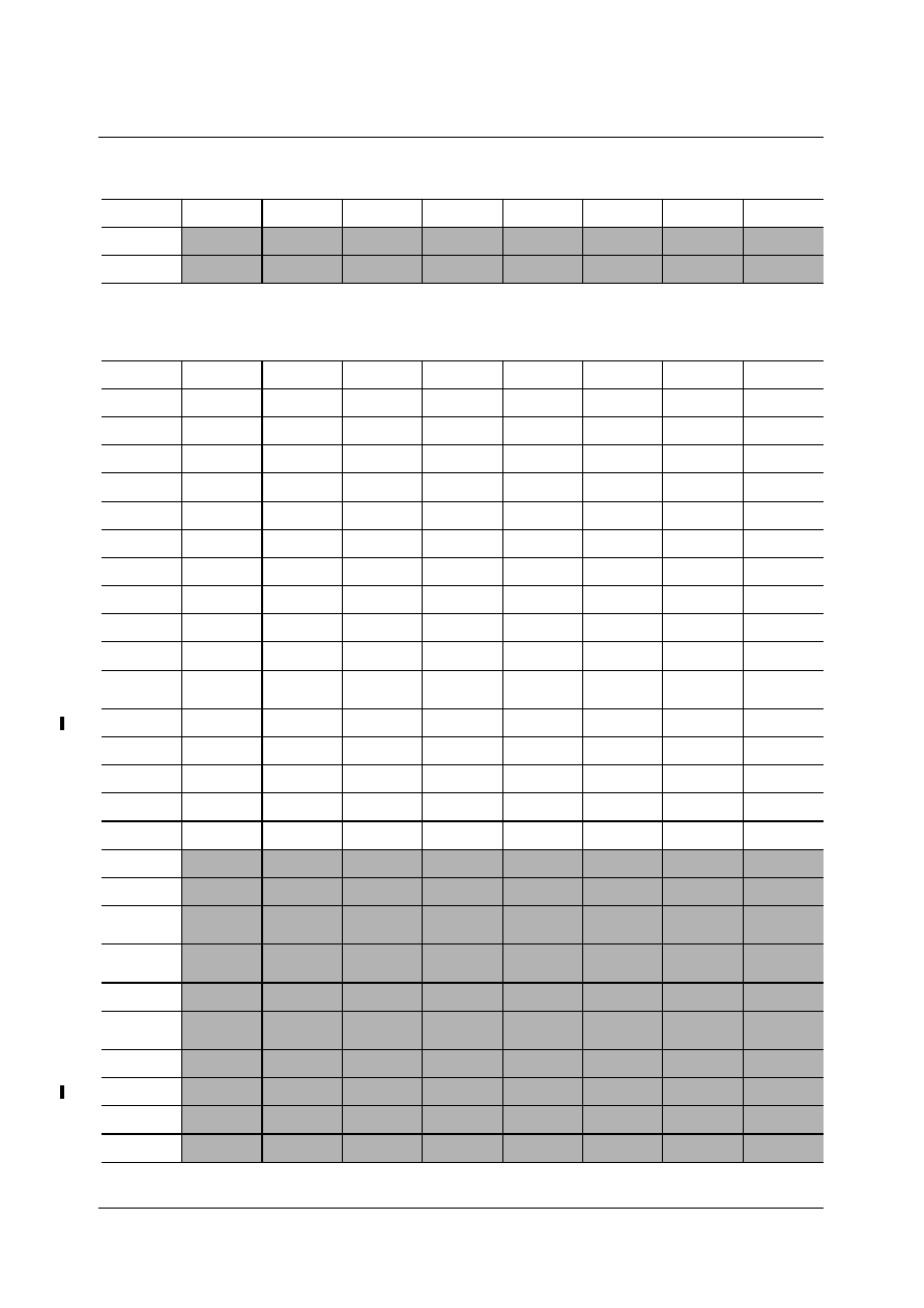
SDA 6000 / SDA 6001
PRELIMINARY DATA SHEET
Version 3.00
Register Overview
13 - 19
Micronas
13.4.2
Registers in ESFR Area
F0
H
R0
R1
R2
R3
R4
R5
R6
R7
F8
H
R8
R9
R10
R11
R12
R13
R14
R15
Address
+ 00
H
+ 01
H
+ 02
H
+ 03
H
+ 04
H
+ 05
H
+ 06
H
+ 07
H
00
H
-
-
-
-
-
-
CPUID
-
08
H
-
-
XADRS1
XADRS2
XADRS3
XADRS4
XADRS5
XADRS6
10
H
FSMOBSA
-
XPERCON
FRXCON
-
-
-
-
18
H
-
-
-
-
-
-
reserved
reserved
20
H
reserved
reserved
reserved
-
-
-
-
-
28
H
-
-
-
-
-
-
-
-
30
H
-
-
-
-
COMDATA
RWDATA
IOSR
-
38
H
IDRT
IDSCU
-
IDMEM2
IDPROG
IDMEM
IDCHIP
IDMANUF
40
H
-
-
-
-
-
-
-
-
48
H
-
-
-
-
-
-
-
-
50
H
RGBINTFC
_EN
CLKINTFC
_EN
-
-
-
-
-
-
58
H
SSCTB
SSCRB
SSCBR
reserved
S0ABSTAT
-
-
-
60
H
SCUSLC
SCUSLS
DGWDCON
DGWDSNT
reserved
-
RTCRELL
RTCRELH
68
H
T14REL
T14
RTCL
RTCH
reserved
reserved
DCMPLL
DCMPLH
70
H
DCMPGL
DCMPGH
DCMP0L
DCMP0H
DCMP1L
DCMP1H
DCMP2L
DCMP2H
78
H
DTREVT
-
DSWEVT
-
DEXEVT
-
DBGSR
-
80
H
EBIREF
-
-
-
RP0H
-
-
-
88
H
-
-
XBCON1
XBCON2
XBCON3
XBCON4
XBCON5
XBCON6
90
H
TOXDGI
TOXGAA
TOXGAB
TOXSRU
AMIWDCO
N
AMIWDSN
T
ALTSEL0P
6
-
98
H
TOXAMI
TOXICACH
E
TOXDCAC
HE
TOXACI
-
-
-
-
A0
H
FRXDGI
FRXGAA
FRXGAB
FRXSRU
SCR2
-
-
-
A8
H
FRXAMI
FRXICACH
E
FRXDCAC
HE
FRXACI
-
-
-
-
B0
H
-
-
-
-
-
-
-
-
B8
H
-
HSDISIC
VSDISIC
ACQIC
ADWIC
ABSTOIC
-
-
C0
H
PECCLIC
-
I
2
CTEIC
-
-
-
I
2
CPIC
-
C8
H
-
-
I
2
CTIC
-
PXDEL
-
S0TBIC
RTCIC
Address
+ 00
H
+ 01
H
+ 02
H
+ 03
H
+ 04
H
+ 05
H
+ 06
H
+ 07
H
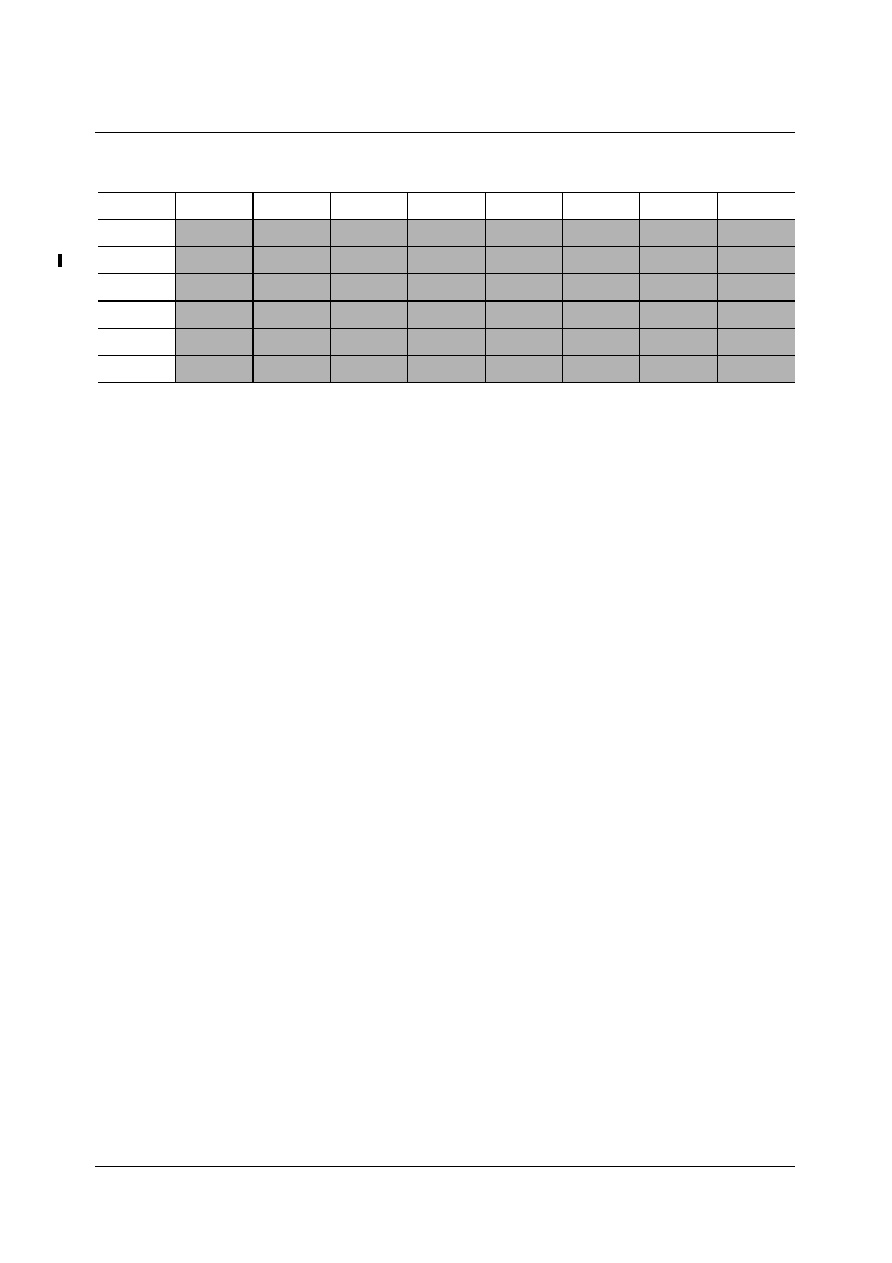
SDA 6000 / SDA 6001
PRELIMINARY DATA SHEET
Version 3.00
Register Overview
13 - 20
Micronas
D0
H
STRVBI
ACQISN
GPRGCRL
GPRGCRH
SCR
VLR
HPR
SDV
D8
H
SDH
HCR
DACCON
PFR
S0ABCON
REDIR
EBICON
EBIDIR
E0
H
EXICON
P5BEN
OSCCON
ODP3
RTCISNC
REDIR1
RTCCON
ODP6
E8
H
SYSCON2
-
SYSCON3
-
-
EXISEL
SYSCON1
ISNC
F0
H
R0
R1
R2
R3
R4
R5
R6
R7
F8
H
R8
R9
R10
R11
R12
R13
R14
R15
Address
+ 00
H
+ 01
H
+ 02
H
+ 03
H
+ 04
H
+ 05
H
+ 06
H
+ 07
H

Elelctrical Characteristics

SDA 6000 / SDA 6001
PRELIMINARY DATA SHEET
Version 3.00
Electrical Characteristics
14 - 3
Micronas
14
Electrical Characteristics
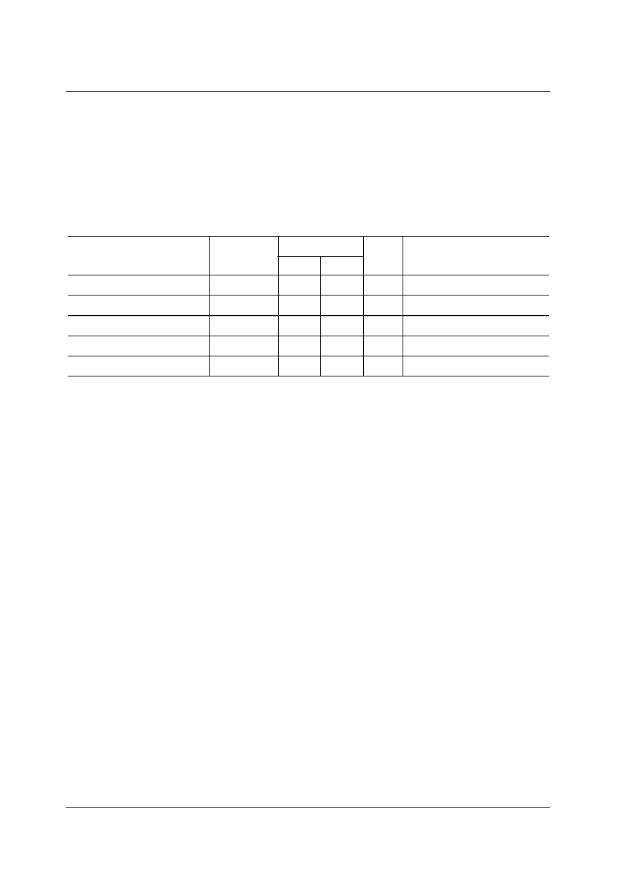
SDA 6000 / SDA 6001
PRELIMINARY DATA SHEET
Version 3.00
Electrical Characteristics
14 - 4
Micronas
14.1
Absolute Maximum Ratings
Note: The maximum ratings may not be exceeded under any circumstances, not even
momentarily and individually, as permanent damage to the IC will result.
Table 14-1
Ambient Temperature
T
A
= 0
�
C ... + 70
�
C
Parameter
Symbol
Limit Values Unit
Test Condition
min.
max.
Supply voltage 3.3 V
V
DD33 1-7
�
4.0
V
�
Supply voltage 2.5 V
V
DD25 1-2
�
3.0
V
�
Analog supply voltage
V
DDA 1-4
�
3.0
V
�
Storage temperature
T
stg
� 20
125
�
C
�
Electrostatic discharge
�
2000
�
V
100 pF, 1.5 k
HBM
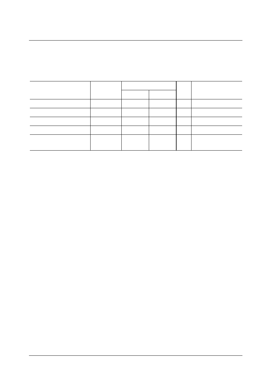
SDA 6000 / SDA 6001
PRELIMINARY DATA SHEET
Version 3.00
Electrical Characteristics
14 - 5
Micronas
14.2
Operating Range
Note: In the operating range, the functions given in the circuit description are fulfilled.
Table 14-2 Operating Range
Parameter
Symbol
Limit Values
Unit Test Condition
min.
max.
Ambient temperature
T
A
0
70
�
C
�
Supply voltage 3.3 V
V
DD33 1-7
3.1
3.6
V
�
Supply voltage 2.5 V
V
DD25 1-2
2.25
2.75
V
�
Analog supply voltage
V
DDA 1-4
2.25
2.75
V
�
Total Power
Consumption
P
total
�
1.5
W
�
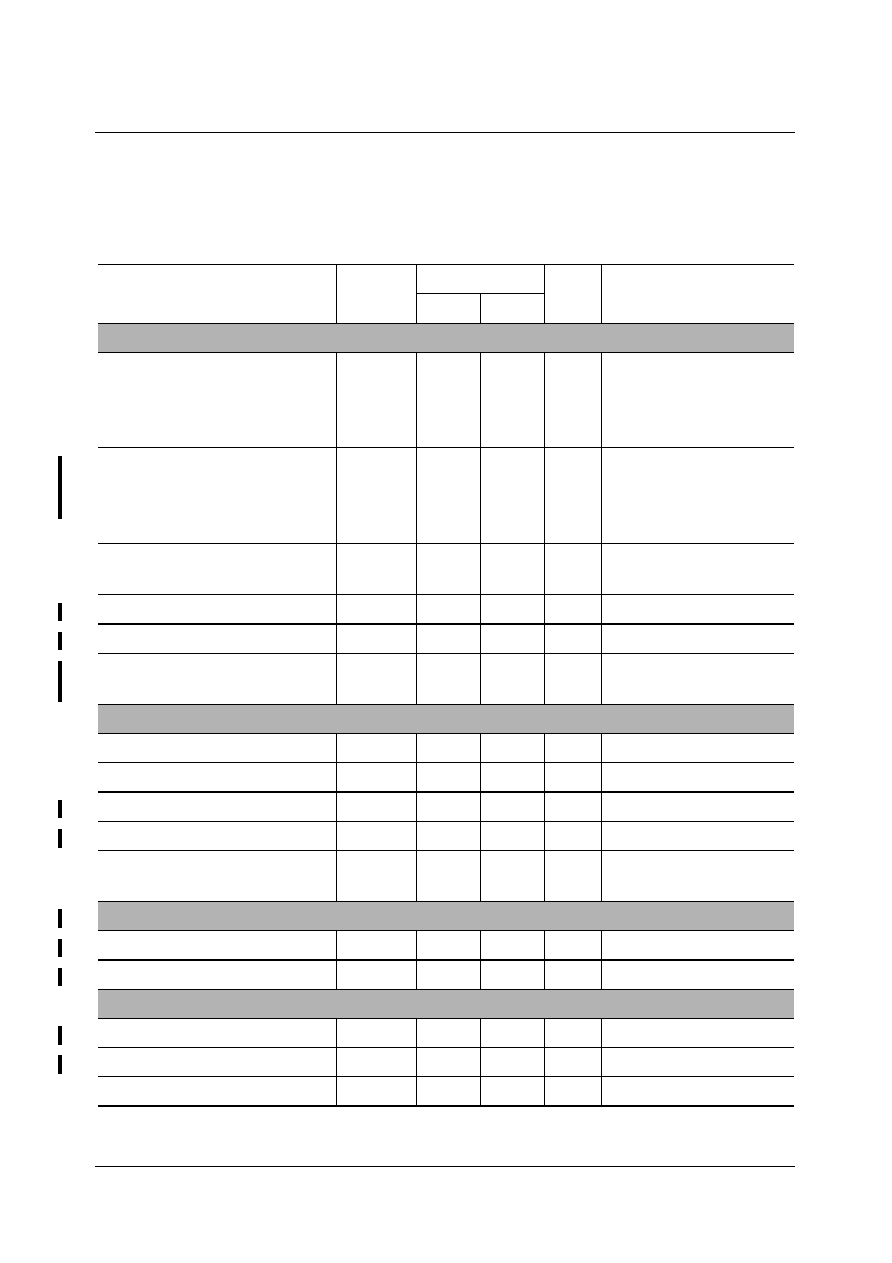
SDA 6000 / SDA 6001
PRELIMINARY DATA SHEET
Version 3.00
Electrical Characteristics
14 - 6
Micronas
14.3
DC Characteristics
Table 14-3
DC Characteristics
Parameter
Symbol Limit Values
Unit
Test Condition
min.
max.
Supply Currents
Supply current (digital) for
3.3 V domain
I
3.3 V
�
150
mA
all ports as inputs,
f
pixel
= 50 MHz,
100 MHz bus
configuration
Supply current (digital +
analog) for 2.5 V domain
I
2.5 V
�
190
expec
ted
(t.b.d)
mA
f
pixel
= 50 MHz,
100 MHz bus
configuration
Analog Power Supply
Current
I
ANA
�
100
mA
�
Idle mode supply current
I
IDLE
�
12
mA
2.5V supply domain
Sleep mode supply current
I
SLEEP
�
1.2
mA
2.5V supply domain
Power down mode supply
current
I
PWDN
�
0.7
mA
2.5V supply domain
I/O Voltages (valid for any pin unless otherwise stated)
Input low voltage
V
IL
� 0.4
0.8
V
�
Input high voltage
V
IH
2.0
3.6
V
�
Output low voltage
V
OL
�
0.45
V
@ I=-6mA
Output high voltage
V
OH
2.5
�
V
@ I= 8mA
Leakage current
I
IL
�
0.2
�
A
@ 0.5 V <
V
in
< (
V
IHNOM
� 0.5 V)
I/O Voltages (valid for all I�C pins: P6.3, P6.4, P6.6, P3.0, P3.1)
Input low voltage
V
IL
� 0.4
1.2
V
�
Input high voltage
V
IH
2.4
3.6
V
�
Crystal Oscillator: XTAL1(input), XTAL2(output)
XTAL1 input low voltage
V
IL
-0.4
0.8
V
XTAL1 input high voltage
V
IH
2.0
3.6
V
Amplifier Transconductance �
�
4.2
mS
�

SDA 6000 / SDA 6001
PRELIMINARY DATA SHEET
Version 3.00
Electrical Characteristics
14 - 7
Micronas
Oscillation Frequency
C
FB
6.0 �
50
ppm
6.0 +
50
ppm
MHz �
Duty Cycle
�
45
55
%
�
High time
t
H
50
�
ns
�
Pin capacitance (XTAL1)
C
I
�
3.5
pF
�
CVBS-Input: CVBS1A (ADC_DIFF = 0; differential CVBS Input)
Pin capacitance
C
P
�
�
pF
�
Input impedance
Z
P
�
�
1/M
�
Ext. coupling capacitance
C
CPL1,2
10
100
nF
�
Source impedance
�
�
< 500
�
Overall CVBS amplitude
V
CVBS
0.75
1.3
V
�
CVBS sync amplitude
V
SYNC
0.18
0.6
V
�
TXT data amplitude
V
DATA
0.3
0.7
V
�
De-coupling Capacitors to
V
DDA
at Pins CVBSi
C
Dec_CPL
�
�
nF
�
CVBS-Input: CVBS1A (ADC_DIFF = 1; non-differential CVBS Input)
Pin capacitance
C
P
�
�
pF
�
Input impedance
Z
P
�
�
1/M
�
Ext. coupling capacitance
C
CPL1
10
100
nF
�
Source impedance
�
< 500
�
Overall CVBS amplitude
V
CVBS
0.75
1.3
V
�
CVBS sync amplitude
V
SYNC
0.18
0.6
V
�
TXT data amplitude
V
DATA
0.3
0.7
V
�
De-coupling Capacitors to
V
DDA
at Pins CVBSi
C
Dec_CPL
�
�
nF
�
CVBS-Input: CVBS2
Pin capacitance
C
P
�
�
pF
�
Input impedance
Z
P
�
�
1/M
�
Ext. coupling capacitance
C
CPL
10
100
nF
�
Table 14-3
DC Characteristics
(cont'd)
Parameter
Symbol Limit Values
Unit
Test Condition
min.
max.
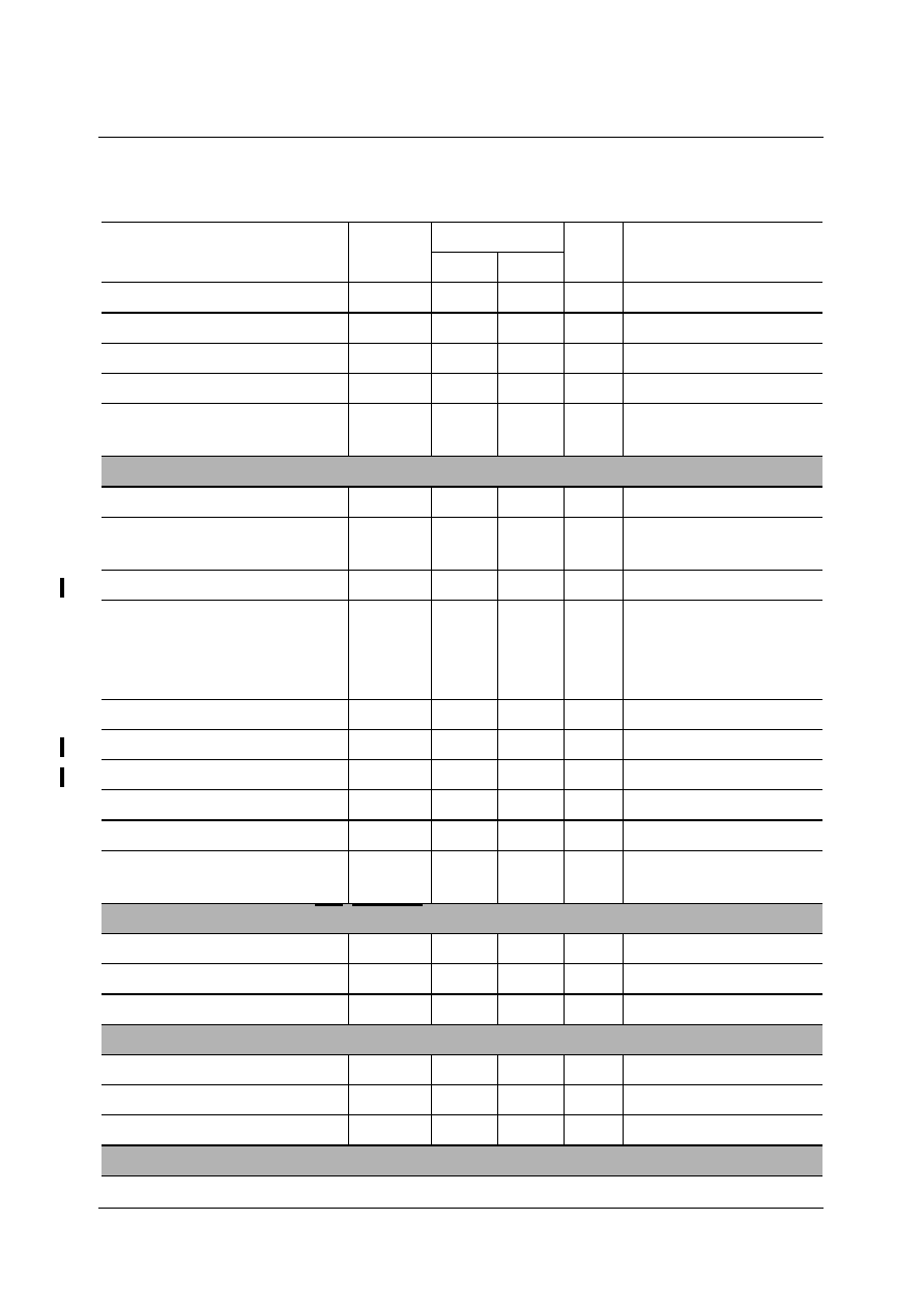
SDA 6000 / SDA 6001
PRELIMINARY DATA SHEET
Version 3.00
Electrical Characteristics
14 - 8
Micronas
Source impedance
�
�
< 500
�
Overall CVBS amplitude
V
CVBS
0.75
1.3
V
�
CVBS sync amplitude
V
SYNC
0.18
0.6
V
�
TXT data amplitude
V
DATA
0.3
0.7
V
�
De-coupling Capacitors to
V
DDA
at Pins CVBSi
C
Dec_CPL
�
�
nF
�
RGB-Outputs
Load capacitance
C
P
�
20
pF
�
Output voltage swing
V
outpp
0.5
1.2
V
available: 0.5 V; 0.7 V;
1.0 V; 1.2 V
RGB offset
U
offset
0.175 0.375 V
�
Rise/Fall Times
t
RF
8.0
12.5
ns
8.0 ns (50 MHz output
BW)
12.5 ns (32 MHz
output BW)
Load resistance
R
L
10
�
k
�
Diff. non-linearity
�
� 0.7
0.7
LSB
�
Int. non-linearity
�
� 0.7
0.7
LSB
�
Output current tracking
�
�
3
%
�
Skew to COR, Blank
t
skew
� 5
5
ns
�
Jitter to Horizontal Sync
Reference
t
Jit
�
4
ns
�
Address Bits: A0 to A9, RD, CSROM
Output Rise Time
t
r
�
16
ns
(10% - 90%)
Output Fall Time
t
f
�
16
ns
(10% - 90%)
Load Capacitance
C
L
�
35
pF
�
Address Bits: A10 to A15
Output Rise Time
t
r
�
6
ns
(10% - 90%)
Output Fall Time
t
f
�
6
ns
(10% - 90%)
Load Capacitance
C
L
�
35
pF
�
P4.(0 .. 5)
Table 14-3
DC Characteristics
(cont'd)
Parameter
Symbol Limit Values
Unit
Test Condition
min.
max.

SDA 6000 / SDA 6001
PRELIMINARY DATA SHEET
Version 3.00
Electrical Characteristics
14 - 9
Micronas
Output Rise Time
t
r
�
16
ns
(10% - 90%)
Output Fall Time
t
f
�
16
ns
(10% - 90%)
Load Capacitance
C
L
�
35
pF
�
Output Current
I
o
�
8
mA
�
Table 14-3
DC Characteristics
(cont'd)
Parameter
Symbol Limit Values
Unit
Test Condition
min.
max.

SDA 6000 / SDA 6001
PRELIMINARY DATA SHEET
Version 3.00
Electrical Characteristics
14 - 10
Micronas
Data Bits: D0 to D15
Output Rise Time
t
r
�
6
ns
(10% - 90%)
Output Fall Time
t
f
�
6
ns
(10% - 90%)
Load Capacitance
C
L
�
35
pF
�
Pin capacitance
C
I
�
5
pF
�
WR, CSSDRAM, CLKEN, LDQM, UDQM
Output Rise Time
t
r
�
6
ns
(10% - 90%)
Output Fall Time
t
f
�
6
ns
(10% - 90%)
Load Capacitance
C
L
�
35
pF
�
Pin capacitance
C
I
�
5
pF
�
MEMCLK
Output Rise Time
t
r
�
2
ns
(10% - 90%)
Output Fall Time
t
f
�
2
ns
(10% - 90%)
Load Capacitance
C
L
�
20
pF
�
BLANK/CORBLA
Output Rise Time
t
r
8
12.5
ns
(10% - 90%)
Output Fall Time
t
f
8
12.5
ns
(10% - 90%)
Load Capacitance
C
L
�
20
pF
�
BLANK/CORBLA (Control bit CORBL = 0; BLANK only)
Output voltage no data
insertion (Video)
V
i-n
0
0.5
V
�
Output voltage for data
insertion
V
i-y
0.9
�
V
�
BLANK/CORBLA (Control bit CORBL = 1; BLANK and COR)
Output voltage no data
insertion no contrast
reduction
V
ic-n
0
0.5
V
�
Output voltage for contrast
reduction and no data
insertion
V
c-y
0.9
1.2
V
�
Table 14-3
DC Characteristics
(cont'd)
Parameter
Symbol Limit Values
Unit
Test Condition
min.
max.
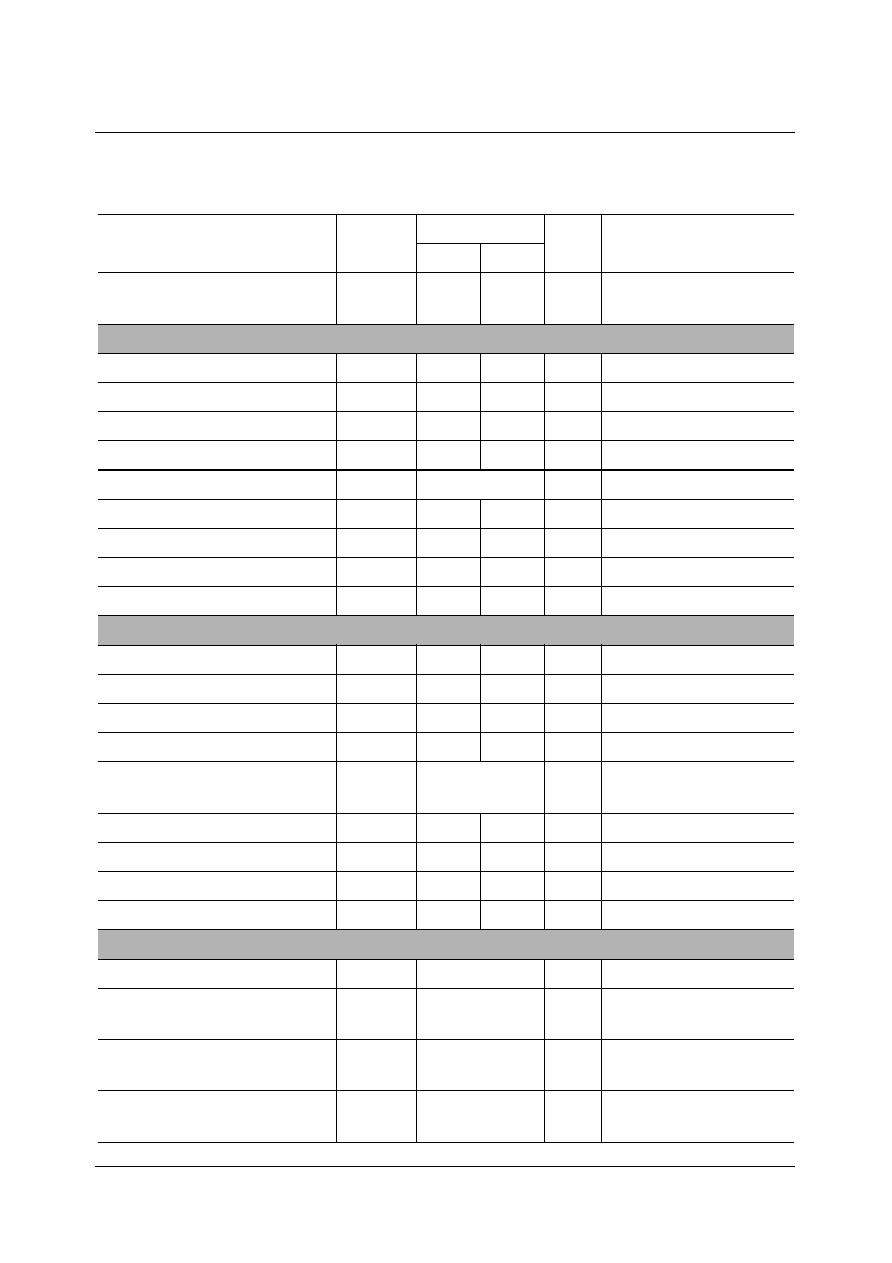
SDA 6000 / SDA 6001
PRELIMINARY DATA SHEET
Version 3.00
Electrical Characteristics
14 - 11
Micronas
Output voltage for data
insertion
V
i-y
1.8
�
V
�
HSYNC
Input Rise Time
t
r
�
100 ns
(10%
-
90%)
Input Fall Time
t
f
�
100
ns
(10% - 90%)
Input Hysteresis
V
HYST
300
600
mV
�
Input Pulse Width
T
IPWH
100
�
ns
�
Output Pulse Width
T
OPWH
1
us
�
Output Rise Time
t
r
�
100
ns
(10% - 90%)
Output Fall Time
t
f
�
100
ns
(10% - 90%)
Load Capacitance
C
L
�
50
pF
�
Pin capacitance
C
I
�
5
pF
�
VSYNC
Input Rise Time
t
r
�
200
ns
(10% - 90%)
Input Fall Time
t
f
�
200
ns
(10% - 90%)
Input Hysteresis
V
HYST
300
600
mV
�
Input Pulse Width
T
IPWV
2/fh
�
�
�
Output Pulse Width
T
IPWV
1/
f
H
�
Depends on Register
HPR
Output Rise Time
t
r
�
100
ns
(10% - 90%)
Output Fall Time
t
f
�
100
ns
(10% - 90%)
Load Capacitance
C
L
�
50
pF
�
Pin capacitance
C
I
�
5
pF
�
VCS Timing (Master mode)
Pulse width of H-Sync
t
HPVCS
4.59
�
s
�
Distance between
Equalizing Impulses
t
DEP
31.98
�
s
�
Pulse Width of Equalizing
Impulses
t
EP
2.31
�
s
�
Pulse Width of Field Sync
Impulses
t
FSP
27.39
�
s
�
Table 14-3
DC Characteristics
(cont'd)
Parameter
Symbol Limit Values
Unit
Test Condition
min.
max.
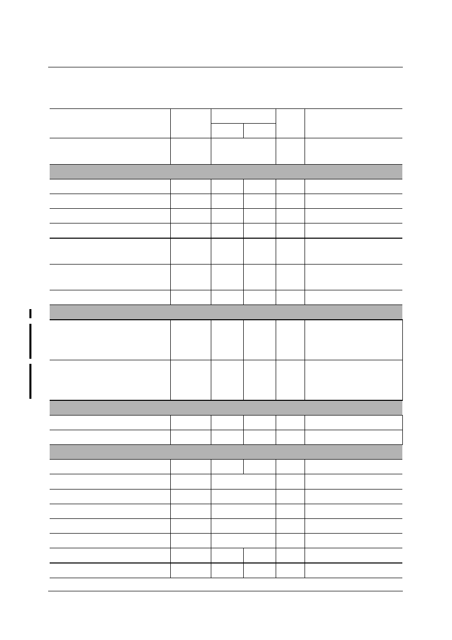
SDA 6000 / SDA 6001
PRELIMINARY DATA SHEET
Version 3.00
Electrical Characteristics
14 - 12
Micronas
Horizontal Period
t
HPR
�
�
s
Depends on Register
HPR
P2.x, P3.x, P5.x, P6.x
Output Rise Time
t
r
�
25
ns
(10% - 90%)
Output Fall Time
t
f
�
25
ns
(10% - 90%)
Load Capacitance
C
L
�
100
pF
�
Pin capacitance
C
I
�
10
pF
�
Input Impedance
(Analog Ports)
Z
P
�
�
1/M
�
Input Sample Frequency
(General Purpose Ports)
F
S
�
33
MHz �
Output Current
I
o
�
8
mA
�
P4.x
Pull up low current
I
IL
11.6
(2.9 in
A23
version)
33
(8.2 in
A23
version)
uA
@V
IL MAX
Pull up high current
I
IH
8.7
(2.2 in
A23
version)
28
(7.1 in
A23
version)
uA
@V
IH MIN
P6.x
Pull up low current
I
Il
2.9
8.2
uA
@V
IL MAX
Pull up high current
I
IH
2.2
7.1
uA
@V
IH MIN
A/D Converter Characteristics (Port 5.0 to P5.3)
Input Voltage Range
V
ain
0
2.5
V
�
ADC Resolution
RES
8
BIT
binary
Output during Underflow
�
0
�
�
Output during Overflow
�
255
�
�
Bandwidth
�
10.5
kHz
�
Sampling Time
t
S
2
�
s
�
Sampling Frequency
f
SAM
21
�
kHz
�
Input Source Resistance
R
S
�
100
k
�
Table 14-3
DC Characteristics
(cont'd)
Parameter
Symbol Limit Values
Unit
Test Condition
min.
max.

SDA 6000 / SDA 6001
PRELIMINARY DATA SHEET
Version 3.00
Electrical Characteristics
14 - 13
Micronas
Pin capacitance
(Analog Ports)
C
P
�
40
pF
�
Reset RSTIN
Pin capacitance
C
I
�
5
pF
�
Reset In Pull Up Resistor
R
pullup
47
100
k
�
Input High Voltage
U
IH
2.0
3.6
V
�
Input Low Voltage
U
IL
-0.4
0.8
V
�
Table 14-3
DC Characteristics
(cont'd)
Parameter
Symbol Limit Values
Unit
Test Condition
min.
max.
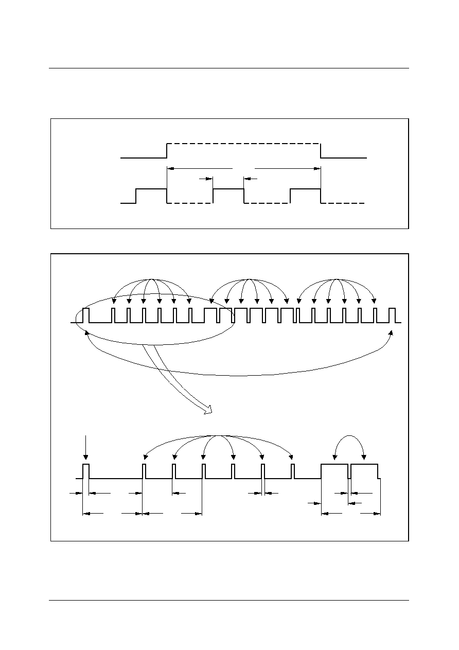
SDA 6000 / SDA 6001
PRELIMINARY DATA SHEET
Version 3.00
Electrical Characteristics
14 - 14
Micronas
14.4
Timings
Figure 14-1 H/V - Sync-Timing (Sync-master mode)
Figure 14-2 VCS -Timing (Sync-master mode)
UET11193
HSYNC
VSYNC
OPWH
t
OPWV
t
Line i
Line i+1
Line i+2
UET11194
CS
V
Equalizing Pulses
Field Sync Pulses
Equalizing Pulses
Horizontal Pulses
Equalizing Pulses
Horizontal Pulse
Field Sync Pulses
V
CS
HPVCS
t
t
HPR
t
HPR
DEP
t
EP
t
t
t
FSP
HPR
t
HPVCS

SDA 6000 / SDA 6001
PRELIMINARY DATA SHEET
Version 3.00
Electrical Characteristics
14 - 15
Micronas
14.5
Package Outlines
P-MQFP-128-2
(Plastic Metric Quad Flat Package)
GP
M0
92
33
Sorts of Packing
Package outlines for tubes, trays etc. are contained in our
Data Book "Package Information".
Dimensions in mm
SMD = Surface Mounted Device

All information and data contained in this data sheet are without any
commitment, are not to be considered as an offer for conclusion of a
contract, nor shall they be construed as to create any liability. Any new
issue of this data sheet invalidates previous issues. Product availability
and delivery are exclusively subject to our respective order confirmation
form; the same applies to orders based on development samples deliv-
ered. By this publication, Micronas GmbH does not assume responsibil-
ity for patent infringements or other rights of third parties which may
result from its use.
Further, Micronas GmbH reserves the right to revise this publication and
to make changes to its content, at any time, without obligation to notify
any person or entity of such revisions or changes.
No part of this publication may be reproduced, photocopied, stored on a
retrieval system, or transmitted without the express written consent of
Micronas GmbH.
SDA 6000, SDA 6001
PRELIMINARY DATA SHEET
433
Micronas
Micronas GmbH
Hans-Bunte-Strasse 19
D-79108 Freiburg (Germany)
P.O. Box 840
D-79008 Freiburg (Germany)
Tel. +49-761-517-0
Fax +49-761-517-2174
E-mail: docservice@micronas.com
Internet: www.micronas.com
Printed in Germany
Order No. 6251-557-2PD