LX3055
P
RODUCTION
D
ATA
S
HEET
Microsemi
Integrated Products Division
11861 Western Avenue, Garden Grove, CA. 92841, 714-898-8121, Fax: 714-893-2570
Page 1
Copyright
© 2004
Rev. 1.0, 2004-07-26
WWW
.
Microse
m
i
.
CO
M
Coplanar InGaAs/InP PIN Photo Diode
TM
Æ
D E S C R I P T I O N
Microsemi's InGaAs/InP PIN
Photo Diode chips are ideal for high
bandwidth 1310nm and 1550nm
optical networking applications.
The device series offers high
responsivity, low dark current, and
high bandwidth for high performance
and low sensitivity receiver design.
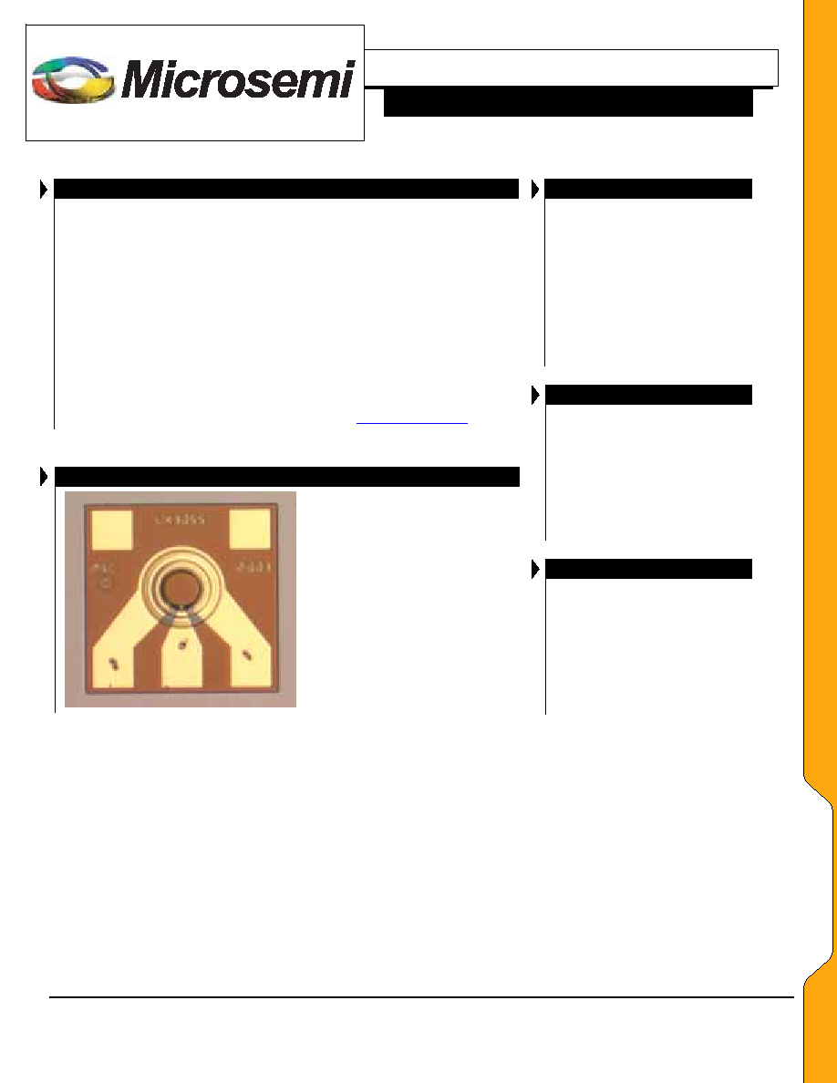
The LX3055 4 Gbps coplanar
waveguide photodiode is currently
offered in die form allowing
manufacturers the versatility of
custom assembly configurations
including traditional wirebond or flip
chip assembly
This device is ideal for
manufacturers of optical receivers,
transponders, optical transmission
modules and combination PIN photo
diode ≠ transimpedance amplifier.
IMPORTANT:
For the most current data, consult
MICROSEMI
's website:
http://www.microsemi.com
P R O D U C T H I G H L I G H T
Coplanar Design (gnd-signal-
gnd) 50 characteristic
impedance
125µm standard pad pitch for
ease of test
Large 75µm x 75µm pad size for
ease of packaging
Wire bond or Flip Chip capability
K E Y F E A T U R E S
LX3055 single die
Coplanar Waveguide , 50
High Responsivity
Low Dark Current
High Bandwidth
Anode/Cathode on
Illuminated Side
125µm Pad pitch
Die good for bond wire or
flip chip applications
A P P L I C A T I O N S
4 Gigabit Fiber Channel
1310nm CATV Optical
Applications
SONET/SDH OC-48, ATM
2.5Gb/s or 3.125Gb/s
Ethernet
1310nm VCSEL receivers
Optical Backplane
B E N E F I T S
Large wire bond contact
pads
Low contact resistance
Wire bond or flip chip
applications
Ground- Signal-Ground pad
configuration for standard
RF test probes
L
L
X
X
3
3
0
0
5
5
5
5

LX3055
P
RODUCTION
D
ATA
S
HEET
Microsemi
Integrated Products Division
11861 Western Avenue, Garden Grove, CA. 92841, 714-898-8121, Fax: 714-893-2570
Page 2
Copyright
© 2004
Rev. 1.0, 2004-07-26
WWW
.
Microse
m
i
.
CO
M
Coplanar InGaAs/InP PIN Photo Diode
TM
Æ
A B S O L U T E M A X I M U M R A T I N G S
Operating Junction Temperature.....................................................................-20 to +85 ∞C
Storage Temperature Range..........................................................................-55 to +125 ∞C
Maximum Soldering Temperature (10 seconds maximum) ...................................... 260 ∞C
Note: Exceeding these ratings could cause damage to the device.
P A C K A G E P I N O U T
p Conta
c
t
n Conta
c
t
(C
a
t
h
o
de
)
n Conta
c
t
LX3055
E L E C T R I C A L C H A R A C T E R I S T I C S
Test conditions: T
A
= 25∞C, V
R
= 2V
LX3055
Parameter Symbol
Test
Conditions
Min Typ Max
Units
ELECTRICAL CHARACTERISTICS
Active Area Diameter
60
µm
VR = 2V,
= 1550nm
0.85 1.0
Responsivity
1
R
VR = 2V,
= 1310nm
0.80 0.90
A/W
Dark
Current
I
D
VR = 5V
0.6
6
nA
Breakdown
Voltage
BV
R
IR = 10µA
30
44
V
Capacitance
C
VR = 2V
0.35
0.40
pF
Bandwidth
2
BW
VR = 2V,
= 1550nm @ - 3dB
6.5 8 GHz
Note: 1. Antireflective coating is º wavelength @ 1430nm covering 1310 and 1550nm applications
2. Bandwidth is measured @ -3dB electrical power (photocurrent drops to 71% of DC value)
A P P L I C A T I O N C I R C U I T S
R
DIODE
C
SHUNT
L
SER1
R
SER
C
DIODE
L
SER2
CPW
Pads
Figure x ≠
Typical VRM Application
Results
RSET (Ohm)
LSER1 (pH)
LSER2 (pH)
CSHUNT (fF)
CDIODE (fF)
RDIODE (M Ohm)
LX3055 20.1
1.6
1.5
7.1
311
730
P
P
A
A
C
C
K
K
A
A
G
G
E
E
D
D
A
A
T
T
A
A

LX3055
P
RODUCTION
D
ATA
S
HEET
Microsemi
Integrated Products Division
11861 Western Avenue, Garden Grove, CA. 92841, 714-898-8121, Fax: 714-893-2570
Page 3
Copyright
© 2004
Rev. 1.0, 2004-07-26
WWW
.
Microse
m
i
.
CO
M
Coplanar InGaAs/InP PIN Photo Diode
TM
Æ
S P A R E T A B L E
12.5um
A
n
contact
(cathode)
p
contact
n
contact
125.0
250.0
325.0
450um
50um
145um
75um
75um
Y
p
w
v
X
Die Dimension, µm
Pad Dimension,
µm
Active Area,
µm (A)
Y X w v
Pad Pitch, µm (p)
Die thickness, µm
60 450
450
75
75 125
152
N O T E S
P R E C A U T I O N S F O R U S E
ESD protection is important. Standard ESD protection procedures should be employed whenever handling InGaAs PIN photo
diode.
PRODUCTION DATA ≠ Information contained in this document is proprietary to
Microsemi and is current as of publication date. This document may not be modified in
any way without the express written consent of Microsemi. Product processing does not
necessarily include testing of all parameters. Microsemi reserves the right to change the
configuration and performance of the product and to discontinue product at any time.
M
M
E
E
C
C
H
H
A
A
N
N
I
I
C
C
A
A
L
L
S
S
LX3055
P
RODUCTION
D
ATA
S
HEET
Microsemi
Integrated Products Division
11861 Western Avenue, Garden Grove, CA. 92841, 714-898-8121, Fax: 714-893-2570
Page 4
Copyright
© 2004
Rev. 1.0, 2004-07-26
WWW
.
Microse
m
i
.
CO
M
Coplanar InGaAs/InP PIN Photo Diode
TM
Æ
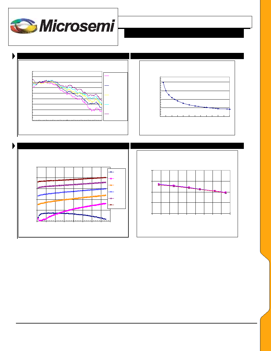
LX3055 Bandwidth (Vr = 1.0V~ 5.0V, at 1550 nm )
3
4
5
6
7
8
9
10
11
12
0
1
2
3
4
5
6
7
8
9
10
Frequency
GHz
R
e
la
t
i
v
e
S
2
1 (
d
B
)
Vr=1.0V:
BW=7.15GHz
Vr=1.5V:
BW=7.50GHz
Vr=2V:
BW=8.00GHz
Vr=3V:
BW=9.55GHz
Vr=5V:
BW=9.95GHz
C-V of LX3055
0.25
0.3
0.35
0.4
0.45
0
5
10
Reverse Bias (V)
C
a
pa
c
i
t
a
nc
e
(
p
F
)
Dark Current vs Voltage over Temperature
1.E-02
1.E-01
1.E+00
1.E+01
1.E+02
1.E+03
0
2
4
6
8
10
12
14
16
Reverse Bias Voltage (V)
Da
r
k
Cu
r
r
e
n
t
(
n
A)
-45 Deg C
-10 Deg C
25 Deg C
50 Deg C
85 Deg C
110 Deg C
Breakdown Voltage vs. Temperature
35
40
45
50
55
-60 -40 -20
0
20
40
60
80 100 120
Temperature ( Deg C)
B
r
eak
d
o
w
n
Vo
l
t
ag
e (
V
)
C
C
H
H
A
A
R
R
T
T
S
S