 | –≠–ª–µ–∫—Ç—Ä–æ–Ω–Ω—ã–π –∫–æ–º–ø–æ–Ω–µ–Ω—Ç: CX29503 | –°–∫–∞—á–∞—Ç—å:  PDF PDF  ZIP ZIP |
500238B
Mindspeed TechnologiesTM
November
Advance Information
2002
Advance Information
This document contains information on a product under development. The parametric information
contains target parameters that are subject to change.
CX29503
Broadband Access Multiplexer (BAM)
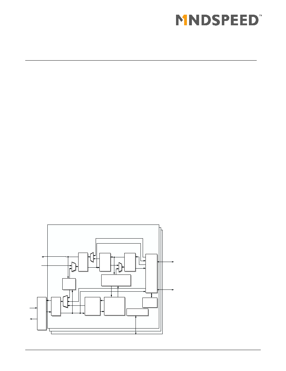
The CX29503 Broadband Access Multiplexer (BAM) is a highly integrated, cost-effective,
monolithic device which performs the mapping, multiplexing, demultiplexing, and framing
of three STS-1, AU-3, DS3, E3, or one AU-4 inputs to any valid combination of 84 DS1 or
63 E1 signals. The CX29503 may be used as a SONET/SDH-to-PDH mapper supporting all
standard mappings at 51 Mbps, 2 Mbps, and 1.5 Mbps rates, or it may be used as a PDH
muldem only. It generates and terminates all Virtual Tributary (VT) and Virtual Container
(VC) path overhead. It includes three embedded DS3/E3 framers, three M13/E13
MUX/DEMUX blocks with G.747 support, and 84 embedded DS1 framers and 63
embedded E1 framers. Other features include standards-compliant alarm indicators,
status monitoring and error counters for all supported tributaries, and an embedded
Command and Status Processor (CSP) that offloads major network maintenance activities
from the host processor.
The CX29503, in conjunction with Mindspeed's 1,024-channel HDLC Controller device
(CX28500) and the STS-12/STM-4 SONET/SDH Framer/Multiplexer device (CX29610),
allows equipment suppliers to develop single, high-density, software-configurable system
solutions for datacom and IP path terminating applications supporting both North
American and European transmission standards. The high level of integration drives down
per-port framer cost and dramatically reduces board space requirements. A complete
STS-12/STM-4 system channelized down to DS1/E1 for an IP HDLC packet processing
solution requires only seven devices from Mindspeed.
The CX29503 supports current ANSI, ETSI, ITU, and Telcordia standards with embedded,
enhanced network alarming and maintenance features that reduce real-time requirements
on the host processor. Physical layer support is provided for alarm generation and
detection, error monitoring, and data link maintenance.
Functional Block Diagram
100702_010a
DS1/VT1.5, E1/VT2.0,
DS1/VC-11, and E1/VC-12
Tributary Mapper
STS-1 to
VT1.5/2.0
TUG-2/3 to
VC-11/VC-12
MUX
Time Slot
Bus
Interface
Module
Command
and Status
Processor
E-Bus
Processor Interface
28xVT1.5/VC-11
21xVT2.0/VC-12
Overhead
Termination/
Generation
SLICE 2
SLICE 3
Payload
TSB
Overhead
TSB
E-Bus Interface
To Host Processor
(Optional)
SI-Bus
Interface
DS3/E3 Serial
Interface
Unchannelized DS3/E3
Unchannelized STS-1
SI-Bus
I/F
Top-
Level
SI-Bus
MUX
STS-1 to
DS3/E3
Mapper
DS3/E3
Framer
M13/E13
MUX
DEMUX
28xDS1
21xE1
Framers
SLICE 1
Distinguishing Features
∑
Capacity
≠ Three STS-1 or TUG-3 or DS3 or
E3 line-side inputs
∑
Supports two types of line interfaces:
≠ SONET Interleave Bus (SI-Bus)
interfaces for a parallel data bus
connection to the SONET/SDH
multiplexer devices at the
STS-1/TUG-3 data rates
≠ DS3/E3 serial interfaces for a
connection to Line Interface Units
(LIU)
∑
System Interface
≠ Supports three serial Time Slot
Bus (TSB) interfaces for a
connection to high-density HDLC
controller devices. Time slots can
be configured to transmit DS3/E3,
DS1/E1/J1, STS-1, or VT1.5
payloads
∑
Supports the following multiplexing
modes:
≠ PDH
∑
M13
∑
E13
∑
G.747
≠ SONET/SDH
∑
STS-1/VT1.5
∑
STS-1/VT2.0
∑
TUG-3/VC-11
∑
TUG-3/VC-12
∑
Supports the following mapping
modes:
≠ SONET/PDH
∑
DS3 to STS-1
∑
E3 to STS-1
∑
DS1 to VT1.5
∑
J1 to VT1.5
∑
E1 to VT2.0
≠ SDH/PDH
≠ DS3 to VC-3
∑
E3 to VC-3
∑
DS1 to VC-11
∑
J1 to VC-11
∑
E1 to VC-12
∑
Embedded PDH framers including:
≠ 3 x DS3/E3 framers
≠ 21 x DS2/E2 framers
≠ 84 x DS1/E1/J1 framers

© 2002,
Mindspeed TechnologiesTM, A Conexant Business
All rights reserved.
Information in this document is provided in connection with Mindspeed Technologies ("Mindspeed") products. These materials are
provided by Mindspeed as a service to its customers and may be used for informational purposes only. Mindspeed assumes no
responsibility for errors or omissions in these materials. Mindspeed may make changes to specifications and product descriptions at
any time, without notice. Mindspeed makes no commitment to update the information and shall have no responsibility whatsoever for
conflicts or incompatibilities arising from future changes to its specifications and product descriptions.
No license, express or implied, by estoppel or otherwise, to any intellectual property rights is granted by this document. Except as
provided in Mindspeed's Terms and Conditions of Sale for such products, Mindspeed assumes no liability whatsoever.
THESE MATERIALS ARE PROVIDED "AS IS" WITHOUT WARRANTY OF ANY KIND, EITHER EXPRESS OR IMPLIED, RELATING
TO SALE AND/OR USE OF MINDSPEED PRODUCTS INCLUDING LIABILITY OR WARRANTIES RELATING TO FITNESS FOR A
PARTICULAR PURPOSE, CONSEQUENTIAL OR INCIDENTAL DAMAGES, MERCHANTABILITY, OR INFRINGEMENT OF ANY
PATENT, COPYRIGHT OR OTHER INTELLECTUAL PROPERTY RIGHT. MINDSPEED FURTHER DOES NOT WARRANT THE
ACCURACY OR COMPLETENESS OF THE INFORMATION, TEXT, GRAPHICS OR OTHER ITEMS CONTAINED WITHIN THESE
MATERIALS. MINDSPEED SHALL NOT BE LIABLE FOR ANY SPECIAL, INDIRECT, INCIDENTAL, OR CONSEQUENTIAL
DAMAGES, INCLUDING WITHOUT LIMITATION, LOST REVENUES OR LOST PROFITS, WHICH MAY RESULT FROM THE USE
OF THESE MATERIALS.
Mindspeed products are not intended for use in medical, lifesaving or life sustaining applications. Mindspeed customers using or
selling Mindspeed products for use in such applications do so at their own risk and agree to fully indemnify Mindspeed for any
damages resulting from such improper use or sale.
The following are trademarks of Conexant Systems, Inc.: Mindspeed TechnologiesTM, the MindspeedTM logo, and "Build It First"TM.
Product names or services listed in this publication are for identification purposes only, and may be trademarks of third parties.
Third-party brands and names are the property of their respective owners.
For additional disclaimer information, please consult Mindspeed Technologies Legal Information posted at
www.mindspeed.com
which is incorporated by reference.
ii
Mindspeed TechnologiesTM
500238B
Advance Information
Ordering Information
Model Number
Package
Operating Temperature
CX29503
TBGA
-40
∞C to 85 ∞C

500238B
Mindspeed TechnologiesTM
iii
Advance Information
∑
Receive and mapping operation
using built-in digital jitter
attenuators; external PLL not
required.
∑
Standards-compliant Performance
Monitoring (PM) at the DS3/E3,
DS1/E1, VT1.5/VT2.0 levels.
STS-1-level PM is performed in the
accompanying SONET/SDH
multiplexer device (CX29610).
∑
Standards-compliant network alarm
detection and insertion for both
SONET/SDH and PDH signals.
∑
Dual edge network alarm indicators
reporting start and end of an alarm
condition with corresponding
maskable interrupts.
∑
Detects and counts errors for
SONET/SDH and PDH signals. Error
counter sizes are sufficient to count
one second of errors without counter
saturation in the presence of up to a
10
-3
error rate.
≠ Error counters operate in two
modes:
∑
one-second mode-counter
values are latched on a
one-second boundary
∑
count to saturation mode
∑
Embedded CSP state machine
∑
Performs device access
activities by communicating
with the host processor via
HDLC command/response
packets.
∑
Automates device activities by
internally responding to
network events, reducing
real-time requirements on the
host processor.
∑
Full data link support at the SONET
STS-1/VT1.5/VT2.0. SDH VC-11,
VC12, and PDH DS3/E3, DS1/E1/J1
levels.
∑
Full line and system side loopback
support:
≠ Line loopbacks: STS-1/TUG-3,
DS3/E3, DS2/E2, DS1/E1/J1
≠ System loopbacks: STS-1,
DS3/E3
∑
Complies with GR 253-CORE,
TR-TSY-000009, T1.105, T1.231, T1.403,
T1.404, G.707, G.742, G.743, G.747,
G.751, G.752, G.781, G.783, ETS300.147,
ETS300.417-1-1
≠ Power Supplies/Power
Consumption
≠ Requires 3.3 V and 1.8 V power
supplies
∑
3.3 V input/output
∑
1.8 V core
∑
Optional 5 V power supply for
5 V input tolerance
∑
Power consumption
≠ under 2 Watts
∑
Package: 31 mm, 324 ball TPBGA
with a heat spreader.
∑
Operating temperature: ≠40 to 85 ∞C
∑
Testing: JTAG boundary scan
support
Applications
∑
Routers
∑
Access Concentrators
∑
Multiservice Switches
∑
T1/T3 Frame Relay Switches

500238B
Mindspeed TechnologiesTM
iv
Advance Information

500238B
Mindspeed TechnologiesTM
i
Advance Information
Contents
Figures
. . . . . . . . . . . . . . . . . . . . . . . . . . . . . . . . . . . . . . . . . . . . . . . . . . . . . . . .xvii
Tables
. . . . . . . . . . . . . . . . . . . . . . . . . . . . . . . . . . . . . . . . . . . . . . . . . . . . . . . . xix
1.0 Product Description. . . . . . . . . . . . . . . . . . . . . . . . . . . . . . . . . . . . . . . . . . . . . . 1-1
1.1
Overview . . . . . . . . . . . . . . . . . . . . . . . . . . . . . . . . . . . . . . . . . . . . . . . . . . . . . . . . . . . . . . . . . . . . . . . 1-1
1.2
Line Side Interfaces . . . . . . . . . . . . . . . . . . . . . . . . . . . . . . . . . . . . . . . . . . . . . . . . . . . . . . . . . . . . . . . 1-2
1.2.1
Line Side Serial Interface . . . . . . . . . . . . . . . . . . . . . . . . . . . . . . . . . . . . . . . . . . . . . . . . . . . . 1-2
1.2.2
SONET Interleave Bus (SI-Bus) Interface . . . . . . . . . . . . . . . . . . . . . . . . . . . . . . . . . . . . . . . . 1-2
1.3
System Side Interfaces≠Time Slot Bus (TSB) . . . . . . . . . . . . . . . . . . . . . . . . . . . . . . . . . . . . . . . . . . . 1-3
1.4
Supported Multiplexing . . . . . . . . . . . . . . . . . . . . . . . . . . . . . . . . . . . . . . . . . . . . . . . . . . . . . . . . . . . . 1-3
1.5
Supported Mapping. . . . . . . . . . . . . . . . . . . . . . . . . . . . . . . . . . . . . . . . . . . . . . . . . . . . . . . . . . . . . . . 1-4
1.6
Embedded Framers . . . . . . . . . . . . . . . . . . . . . . . . . . . . . . . . . . . . . . . . . . . . . . . . . . . . . . . . . . . . . . . 1-5
1.7
Supported Through-Paths . . . . . . . . . . . . . . . . . . . . . . . . . . . . . . . . . . . . . . . . . . . . . . . . . . . . . . . . . . 1-6
1.7.1
Commonly Used Through-Paths . . . . . . . . . . . . . . . . . . . . . . . . . . . . . . . . . . . . . . . . . . . . . . . 1-8
1.7.2
Other Supported Through-Paths . . . . . . . . . . . . . . . . . . . . . . . . . . . . . . . . . . . . . . . . . . . . . . . 1-9
1.8
Applications. . . . . . . . . . . . . . . . . . . . . . . . . . . . . . . . . . . . . . . . . . . . . . . . . . . . . . . . . . . . . . . . . . . . 1-10
1.8.1
OC-12/STM-4 Path Termination for HDLC Application . . . . . . . . . . . . . . . . . . . . . . . . . . . . . 1-10
1.8.2
OC-3/STM-1 Path Termination for HDLC Application . . . . . . . . . . . . . . . . . . . . . . . . . . . . . . 1-11
1.8.3
DS3/E3 Path Termination for HDLC Application . . . . . . . . . . . . . . . . . . . . . . . . . . . . . . . . . . 1-11
1.9
Pin Assignments . . . . . . . . . . . . . . . . . . . . . . . . . . . . . . . . . . . . . . . . . . . . . . . . . . . . . . . . . . . . . . . . 1-12
2.0 Functional Description. . . . . . . . . . . . . . . . . . . . . . . . . . . . . . . . . . . . . . . . . . . . 2-1
2.1
CX29503 Block Diagram . . . . . . . . . . . . . . . . . . . . . . . . . . . . . . . . . . . . . . . . . . . . . . . . . . . . . . . . . . . 2-1
2.2
CX29503 Detailed Block Diagram . . . . . . . . . . . . . . . . . . . . . . . . . . . . . . . . . . . . . . . . . . . . . . . . . . . . 2-3
2.3
Top-Level MUX . . . . . . . . . . . . . . . . . . . . . . . . . . . . . . . . . . . . . . . . . . . . . . . . . . . . . . . . . . . . . . . . . . 2-4
2.4
Global Control and Status Block . . . . . . . . . . . . . . . . . . . . . . . . . . . . . . . . . . . . . . . . . . . . . . . . . . . . . 2-4
2.5
SONET Interleave Bus (SI-Bus) . . . . . . . . . . . . . . . . . . . . . . . . . . . . . . . . . . . . . . . . . . . . . . . . . . . . . . 2-5
2.5.1
SI-Bus Operation. . . . . . . . . . . . . . . . . . . . . . . . . . . . . . . . . . . . . . . . . . . . . . . . . . . . . . . . . . . 2-6
2.5.1.1 Transmit Interface . . . . . . . . . . . . . . . . . . . . . . . . . . . . . . . . . . . . . . . . . . . . . . . 2-7
2.5.1.2 Receive Interface . . . . . . . . . . . . . . . . . . . . . . . . . . . . . . . . . . . . . . . . . . . . . . . . 2-8
2.5.2
CX29503 Connection to CX29610 . . . . . . . . . . . . . . . . . . . . . . . . . . . . . . . . . . . . . . . . . . . . . . 2-9
2.6
SONET/SDH Mapper/Multiplexer (MUX) Block . . . . . . . . . . . . . . . . . . . . . . . . . . . . . . . . . . . . . . . . . 2-10
2.6.1
SONET/SDH Mapper/MUX Receiver . . . . . . . . . . . . . . . . . . . . . . . . . . . . . . . . . . . . . . . . . . . 2-12
2.6.1.1 SI-Bus Receiver Interface . . . . . . . . . . . . . . . . . . . . . . . . . . . . . . . . . . . . . . . . 2-12
2.6.1.2 STS-1/TUG-3 SPE Extraction Control . . . . . . . . . . . . . . . . . . . . . . . . . . . . . . . 2-12

Contents
CX29503 Data Sheet
ii
Mindspeed TechnologiesTM
500238B
Advance Information
l
2.6.1.3 DS3/E3 Demapping Function. . . . . . . . . . . . . . . . . . . . . . . . . . . . . . . . . . . . . . 2-12
2.6.1.4 DS3/E3 Smoothing Function . . . . . . . . . . . . . . . . . . . . . . . . . . . . . . . . . . . . . . 2-13
2.6.1.5 VT Extraction Control. . . . . . . . . . . . . . . . . . . . . . . . . . . . . . . . . . . . . . . . . . . . 2-13
2.6.1.6 VT Performance Monitoring . . . . . . . . . . . . . . . . . . . . . . . . . . . . . . . . . . . . . . 2-14
2.6.1.7 VT Path Conditioning. . . . . . . . . . . . . . . . . . . . . . . . . . . . . . . . . . . . . . . . . . . . 2-15
2.6.1.8 DS1/E1 Demapping Function. . . . . . . . . . . . . . . . . . . . . . . . . . . . . . . . . . . . . . 2-15
2.6.1.9 Receive Time Slot Bus Interface . . . . . . . . . . . . . . . . . . . . . . . . . . . . . . . . . . . 2-15
2.6.2
SONET/SDH Mapper/MUX Transmitter . . . . . . . . . . . . . . . . . . . . . . . . . . . . . . . . . . . . . . . . . 2-16
2.6.2.1 SI-Bus Transmitter Interface . . . . . . . . . . . . . . . . . . . . . . . . . . . . . . . . . . . . . . 2-16
2.6.2.2 STS-1/TUG-3 Overhead Insertion . . . . . . . . . . . . . . . . . . . . . . . . . . . . . . . . . . 2-16
2.6.2.3 VT Build and VT Overhead Insertion . . . . . . . . . . . . . . . . . . . . . . . . . . . . . . . . 2-16
2.6.2.4 DS3/E3 Mapping Function . . . . . . . . . . . . . . . . . . . . . . . . . . . . . . . . . . . . . . . . 2-17
2.6.2.5 DS1/E1 Mapping Function . . . . . . . . . . . . . . . . . . . . . . . . . . . . . . . . . . . . . . . . 2-17
2.6.2.6 Transmit Time Slot Bus (TSB) Interface . . . . . . . . . . . . . . . . . . . . . . . . . . . . . 2-18
2.6.3
SONET/SDH Transmitter to Receiver Loopback Control . . . . . . . . . . . . . . . . . . . . . . . . . . . . 2-18
2.7
DS3/E3 Framer Block. . . . . . . . . . . . . . . . . . . . . . . . . . . . . . . . . . . . . . . . . . . . . . . . . . . . . . . . . . . . . 2-19
2.8
DS1/E1 Framer Block. . . . . . . . . . . . . . . . . . . . . . . . . . . . . . . . . . . . . . . . . . . . . . . . . . . . . . . . . . . . . 2-23
2.8.1
Module Functions . . . . . . . . . . . . . . . . . . . . . . . . . . . . . . . . . . . . . . . . . . . . . . . . . . . . . . . . . 2-24
2.9
M13/E13 Multiplexer (MUX) Block . . . . . . . . . . . . . . . . . . . . . . . . . . . . . . . . . . . . . . . . . . . . . . . . . . 2-28
2.9.1
Operational Features Specification . . . . . . . . . . . . . . . . . . . . . . . . . . . . . . . . . . . . . . . . . . . . 2-30
2.10
Time Slot Bus (TSB) Interface . . . . . . . . . . . . . . . . . . . . . . . . . . . . . . . . . . . . . . . . . . . . . . . . . . . . . . 2-31
2.10.1
Summary of Payload TSB . . . . . . . . . . . . . . . . . . . . . . . . . . . . . . . . . . . . . . . . . . . . . . . . . . . 2-33
2.10.2
Summary of Overhead TSB. . . . . . . . . . . . . . . . . . . . . . . . . . . . . . . . . . . . . . . . . . . . . . . . . . 2-34
2.10.3
TSB Signals. . . . . . . . . . . . . . . . . . . . . . . . . . . . . . . . . . . . . . . . . . . . . . . . . . . . . . . . . . . . . . 2-35
2.10.4
Details of Payload TSB . . . . . . . . . . . . . . . . . . . . . . . . . . . . . . . . . . . . . . . . . . . . . . . . . . . . . 2-36
2.10.4.1 Data Path Signals . . . . . . . . . . . . . . . . . . . . . . . . . . . . . . . . . . . . . . . . . . . . . . 2-36
2.10.4.2 Stuff Byte Compensation . . . . . . . . . . . . . . . . . . . . . . . . . . . . . . . . . . . . . . . . . 2-36
2.10.4.3 Mapping of Payload to TSB Payload Time Slots . . . . . . . . . . . . . . . . . . . . . . . 2-37
2.10.5
Details of Overhead TSB . . . . . . . . . . . . . . . . . . . . . . . . . . . . . . . . . . . . . . . . . . . . . . . . . . . . 2-41
2.10.5.1 Overhead Data Path . . . . . . . . . . . . . . . . . . . . . . . . . . . . . . . . . . . . . . . . . . . . . 2-41
2.10.5.2 Overhead TSB Frame Stuff Byte Compensation. . . . . . . . . . . . . . . . . . . . . . . . 2-41
2.10.5.3 Mapping of Overhead Data to Overhead TSB Time Slots . . . . . . . . . . . . . . . . . 2-42
2.10.5.4 SONET Overhead Communication Channels . . . . . . . . . . . . . . . . . . . . . . . . . . 2-44
2.10.5.5 SDH Overhead Communication Channels . . . . . . . . . . . . . . . . . . . . . . . . . . . . 2-45
2.10.5.6 Electrical DS3 Serial Port Overhead Communication Channels . . . . . . . . . . . . 2-45
2.10.5.7 Electrical E3 Serial Port Overhead Communication Channels . . . . . . . . . . . . . 2-45
2.10.6
Timing Details . . . . . . . . . . . . . . . . . . . . . . . . . . . . . . . . . . . . . . . . . . . . . . . . . . . . . . . . . . . . 2-46
2.10.6.1 Payload Bus, AC Characteristics . . . . . . . . . . . . . . . . . . . . . . . . . . . . . . . . . . . 2-46
2.10.6.2 Overhead Bus, AC Characteristics . . . . . . . . . . . . . . . . . . . . . . . . . . . . . . . . . . 2-51
3.0 Parallel Microprocessor Interface . . . . . . . . . . . . . . . . . . . . . . . . . . . . . . . . . . . . 3-1
3.1
Address/Data Bus . . . . . . . . . . . . . . . . . . . . . . . . . . . . . . . . . . . . . . . . . . . . . . . . . . . . . . . . . . . . . . . . 3-1
3.2
Bus Control Signals . . . . . . . . . . . . . . . . . . . . . . . . . . . . . . . . . . . . . . . . . . . . . . . . . . . . . . . . . . . . . . . 3-1

500238B
Mindspeed TechnologiesTM
iii
Advance Information
CX29503 Data Sheet
Contents
3.3
Interrupt and Control Signals . . . . . . . . . . . . . . . . . . . . . . . . . . . . . . . . . . . . . . . . . . . . . . . . . . . . . . . 3-2
3.4
Command and Status Processor (CSP). . . . . . . . . . . . . . . . . . . . . . . . . . . . . . . . . . . . . . . . . . . . . . . . 3-3
4.0 Clock Sources and Clock Configurations. . . . . . . . . . . . . . . . . . . . . . . . . . . . . . . . 4-1
4.1
DS3/E3 Framer Clock and Data Options on the Line Side . . . . . . . . . . . . . . . . . . . . . . . . . . . . . . . . . . 4-1
4.2
DS1/E1 Clock and Data Options. . . . . . . . . . . . . . . . . . . . . . . . . . . . . . . . . . . . . . . . . . . . . . . . . . . . . . 4-3
4.3
SI-Bus Interface Mode. . . . . . . . . . . . . . . . . . . . . . . . . . . . . . . . . . . . . . . . . . . . . . . . . . . . . . . . . . . . . 4-4
4.3.1
DS3/E3 Clock and Data Configurations (SI-Bus Interface Mode) . . . . . . . . . . . . . . . . . . . . . . 4-4
4.3.2
DS1/E1 Clock and Data Configurations (SI-Bus Interface Mode) . . . . . . . . . . . . . . . . . . . . . . 4-5
4.4
Serial DS3 Interface Mode. . . . . . . . . . . . . . . . . . . . . . . . . . . . . . . . . . . . . . . . . . . . . . . . . . . . . . . . . . 4-7
4.5
Serial E3 Interface Mode . . . . . . . . . . . . . . . . . . . . . . . . . . . . . . . . . . . . . . . . . . . . . . . . . . . . . . . . . . . 4-8
4.6
Payload TSB and Overhead TSB Clocks. . . . . . . . . . . . . . . . . . . . . . . . . . . . . . . . . . . . . . . . . . . . . . . . 4-9
4.7
Command and Status Processor (CSP) and Microprocessor Clocks. . . . . . . . . . . . . . . . . . . . . . . . . 4-10
4.8
DS1/E1 System and Microprocessor Clocks . . . . . . . . . . . . . . . . . . . . . . . . . . . . . . . . . . . . . . . . . . . 4-12
4.9
One Hertz Clock . . . . . . . . . . . . . . . . . . . . . . . . . . . . . . . . . . . . . . . . . . . . . . . . . . . . . . . . . . . . . . . . . 4-13
5.0 Loopbacks . . . . . . . . . . . . . . . . . . . . . . . . . . . . . . . . . . . . . . . . . . . . . . . . . . . . 5-1
5.1
DS3/E3 Framer and M13 MUX Loopbacks . . . . . . . . . . . . . . . . . . . . . . . . . . . . . . . . . . . . . . . . . . . . . 5-1
5.2
DS1/E1 Framer Loopbacks . . . . . . . . . . . . . . . . . . . . . . . . . . . . . . . . . . . . . . . . . . . . . . . . . . . . . . . . . 5-3
5.3
SI-Bus System Side Loopback . . . . . . . . . . . . . . . . . . . . . . . . . . . . . . . . . . . . . . . . . . . . . . . . . . . . . . 5-4
6.0 Path Conditioning . . . . . . . . . . . . . . . . . . . . . . . . . . . . . . . . . . . . . . . . . . . . . . . 6-1
6.1
STS-1 Path Conditioning . . . . . . . . . . . . . . . . . . . . . . . . . . . . . . . . . . . . . . . . . . . . . . . . . . . . . . . . . . . 6-1
6.2
DS3 Path Conditioning . . . . . . . . . . . . . . . . . . . . . . . . . . . . . . . . . . . . . . . . . . . . . . . . . . . . . . . . . . . . 6-2
6.3
E3 Path Conditioning . . . . . . . . . . . . . . . . . . . . . . . . . . . . . . . . . . . . . . . . . . . . . . . . . . . . . . . . . . . . . . 6-2
6.4
DS2 Path Conditioning . . . . . . . . . . . . . . . . . . . . . . . . . . . . . . . . . . . . . . . . . . . . . . . . . . . . . . . . . . . . 6-3
6.5
E2 Path Conditioning . . . . . . . . . . . . . . . . . . . . . . . . . . . . . . . . . . . . . . . . . . . . . . . . . . . . . . . . . . . . . . 6-3
6.6
VT Path Conditioning. . . . . . . . . . . . . . . . . . . . . . . . . . . . . . . . . . . . . . . . . . . . . . . . . . . . . . . . . . . . . . 6-4
6.7
DS1/E1 Path Conditioning . . . . . . . . . . . . . . . . . . . . . . . . . . . . . . . . . . . . . . . . . . . . . . . . . . . . . . . . . . 6-4
7.0 Register Map . . . . . . . . . . . . . . . . . . . . . . . . . . . . . . . . . . . . . . . . . . . . . . . . . . 7-1
7.1
Top Level--CX29503 Register Map. . . . . . . . . . . . . . . . . . . . . . . . . . . . . . . . . . . . . . . . . . . . . . . . . . . 7-1
7.2
Single Mapper/MUX Block Register Map. . . . . . . . . . . . . . . . . . . . . . . . . . . . . . . . . . . . . . . . . . . . . . . 7-2
8.0 Register Description . . . . . . . . . . . . . . . . . . . . . . . . . . . . . . . . . . . . . . . . . . . . . 8-1
8.1
Global Control and Status . . . . . . . . . . . . . . . . . . . . . . . . . . . . . . . . . . . . . . . . . . . . . . . . . . . . . . . . . . 8-1
0x0000--Device Identification Register (DEV_ID) . . . . . . . . . . . . . . . . . . . . . . . . . . . . . . . . . 8-2

Contents
CX29503 Data Sheet
iv
Mindspeed TechnologiesTM
500238B
Advance Information
l
0x0001--Top Level Control Register (TOP_CTL_REG). . . . . . . . . . . . . . . . . . . . . . . . . . . . . . 8-2
0x0002--Top Level Interrupt Status Register (TOP_IRQ_STAT). . . . . . . . . . . . . . . . . . . . . . . 8-2
0x0003--Top Level Interrupt Enable Register (TOP_IRQ_ENB) . . . . . . . . . . . . . . . . . . . . . . . 8-3
0x0004--DS1/E1 Framer Interrupt Request Register 1 (FR_IRR1) . . . . . . . . . . . . . . . . . . . . 8-3
0x0005--DS1/E1 Framer Interrupt Status Register 2 (FR_IRR2) . . . . . . . . . . . . . . . . . . . . . . 8-4
0x0006--DS1/E1 Framer Interrupt Request Register 3 (FR_IRR3) . . . . . . . . . . . . . . . . . . . . 8-4
0x0007--DS1/E1 Framer Interrupt Request Register 4 (FR_IRR4) . . . . . . . . . . . . . . . . . . . . 8-5
0x0008--DS1/E1 Framer Interrupt Enable Register 1 (FR_IE1) . . . . . . . . . . . . . . . . . . . . . . . 8-5
0x0009--DS1/E1 Framer Interrupt Enable Register 2 (FR_IE2) . . . . . . . . . . . . . . . . . . . . . . . 8-6
0x000A--DS1/E1 Framer Interrupt Enable Register 3 (FR_IE3) . . . . . . . . . . . . . . . . . . . . . . . 8-6
0x000B--DS1/E1 Framer Interrupt Enable Register 4 (FR_IE4) . . . . . . . . . . . . . . . . . . . . . . . 8-7
0x000C--Watchdog Interrupt Status Register 4 (WD_INT_STAT) . . . . . . . . . . . . . . . . . . . . . 8-7
0x000D--Watchdog Interrupt Enable Register (WD_INT_ENB). . . . . . . . . . . . . . . . . . . . . . . 8-7
0x000E--Watchdog Control Register (WD_CTL) . . . . . . . . . . . . . . . . . . . . . . . . . . . . . . . . . . 8-7
8.2
Time Slot Bus (TSB) Interface . . . . . . . . . . . . . . . . . . . . . . . . . . . . . . . . . . . . . . . . . . . . . . . . . . . . . . . 8-8
0x0100 to 0x01EC--Test Registers. . . . . . . . . . . . . . . . . . . . . . . . . . . . . . . . . . . . . . . . . . . . . 8-8
0x01ED ≠ Unframed Link Control Register 1. . . . . . . . . . . . . . . . . . . . . . . . . . . . . . . . . . . . . . 8-8
0x01EE ≠ Unframed Link Control Register 2 . . . . . . . . . . . . . . . . . . . . . . . . . . . . . . . . . . . . . . 8-9
0x01EF ≠ Unframed Link Control Register 3 . . . . . . . . . . . . . . . . . . . . . . . . . . . . . . . . . . . . . . 8-9
0x01F0 ≠ Unframed Link Control Register 4 . . . . . . . . . . . . . . . . . . . . . . . . . . . . . . . . . . . . . . 8-9
0x01F1--Flush FIFO Register . . . . . . . . . . . . . . . . . . . . . . . . . . . . . . . . . . . . . . . . . . . . . . . . 8-10
0x01F2--TSB FIFO Interrupt Status Register (Used for Diagnostics) . . . . . . . . . . . . . . . . . . 8-10
0x01F3--TSB FIFO Interrupt Enable Register (Used for DS1 Diagnostics) . . . . . . . . . . . . . . 8-11
0x01F4--Overflow Tx Payload FIFO Number Status Register (Used for Diagnostics) . . . . . 8-11
0x01F5--Underflow Tx Payload FIFO Number Status Register (Used for Diagnostics) . . . . 8-12
0x01F6--Overflow Rx Payload FIFO Number Status Register (Used for Diagnostics) . . . . . 8-12
0x01F7--Underflow Rx Payload FIFO Number Status Register (Used for Diagnostics) . . . . 8-12
0x01F8--Overflow Tx Overhead FIFO Number Status Register (Used for Diagnostics) . . . . 8-12
0x01F9--Underflow Tx Overhead FIFO Number Status Register (Used for Diagnostics) . . . 8-13
0x01FA--Overflow Rx Overhead FIFO Number Status Register (Used for Diagnostics) . . . . 8-13
0x01FB--Underflow Rx Overhead FIFO Number Status Register (Used for Diagnostics) . . . 8-13
0x01FC--TSB Module Operation . . . . . . . . . . . . . . . . . . . . . . . . . . . . . . . . . . . . . . . . . . . . . 8-14
0x01FE--Framer Set (FS) Configuration Register 1 . . . . . . . . . . . . . . . . . . . . . . . . . . . . . . . 8-14
0x01FF--Framer Set (FS) Configuration Register 2 . . . . . . . . . . . . . . . . . . . . . . . . . . . . . . . 8-15
8.3
DS1/E1 Framers . . . . . . . . . . . . . . . . . . . . . . . . . . . . . . . . . . . . . . . . . . . . . . . . . . . . . . . . . . . . . . . . 8-16
8.3.1
DS1/E1 Framer Set Global Control and Status Register . . . . . . . . . . . . . . . . . . . . . . . . . . . . 8-16
0x00--Framer Control Register 1 (FCR0) . . . . . . . . . . . . . . . . . . . . . . . . . . . . . . . . . . . . . . . 8-16
0x01--Framer Control Register 2 (FCR1) . . . . . . . . . . . . . . . . . . . . . . . . . . . . . . . . . . . . . . . 8-16
8.3.2
DS1/E1 Framer Control and Status Registers . . . . . . . . . . . . . . . . . . . . . . . . . . . . . . . . . . . . 8-17
8.3.2.1 Primary Control Registers . . . . . . . . . . . . . . . . . . . . . . . . . . . . . . . . . . . . . . . . 8-21
0x01--Primary Control Register (CR0) . . . . . . . . . . . . . . . . . . . . . . . . . . . . . . . . . . . . . . . . 8-21
0x03--Interrupt Request Register (IRR) . . . . . . . . . . . . . . . . . . . . . . . . . . . . . . . . . . . . . . . 8-25

500238B
Mindspeed TechnologiesTM
v
Advance Information
CX29503 Data Sheet
Contents
8.3.2.2 Interrupt Status Registers . . . . . . . . . . . . . . . . . . . . . . . . . . . . . . . . . . . . . . . . 8-27
0x04--Alarm 1 Interrupt Status (ISR7) . . . . . . . . . . . . . . . . . . . . . . . . . . . . . . . . . . . . . . . . 8-28
0x05--Alarm 2 Interrupt Status (ISR6) . . . . . . . . . . . . . . . . . . . . . . . . . . . . . . . . . . . . . . . . 8-29
0x06--Error Interrupt Status (ISR5). . . . . . . . . . . . . . . . . . . . . . . . . . . . . . . . . . . . . . . . . . . 8-29
0x07--Counter Overflow Interrupt Status (ISR4) . . . . . . . . . . . . . . . . . . . . . . . . . . . . . . . . . 8-30
0x08--Timer Interrupt Status (ISR3) . . . . . . . . . . . . . . . . . . . . . . . . . . . . . . . . . . . . . . . . . . 8-30
0x09--Data Link 1 Interrupt Status (ISR2) . . . . . . . . . . . . . . . . . . . . . . . . . . . . . . . . . . . . . . 8-31
0x0A--Data Link 2 Interrupt Status (ISR1). . . . . . . . . . . . . . . . . . . . . . . . . . . . . . . . . . . . . . 8-31
0x0B--Pattern Interrupt Status (ISR0) . . . . . . . . . . . . . . . . . . . . . . . . . . . . . . . . . . . . . . . . . 8-32
8.3.2.3 Interrupt Enable Registers (IER) . . . . . . . . . . . . . . . . . . . . . . . . . . . . . . . . . . . 8-32
0x0C--Alarm 1 Interrupt Enable Register (IER7) . . . . . . . . . . . . . . . . . . . . . . . . . . . . . . . . . 8-32
0x0D--Alarm 2 Interrupt Enable Register (IER6) . . . . . . . . . . . . . . . . . . . . . . . . . . . . . . . . . 8-33
0x0E--Error Interrupt Enable Register (IER5) . . . . . . . . . . . . . . . . . . . . . . . . . . . . . . . . . . . 8-33
0x0F--Count Overflow Interrupt Enable Register (IER4) . . . . . . . . . . . . . . . . . . . . . . . . . . . 8-33
0x10--Timer Interrupt Enable Register (IER3) . . . . . . . . . . . . . . . . . . . . . . . . . . . . . . . . . . . 8-34
0x11--Data Link 1 Interrupt Enable Register (IER2). . . . . . . . . . . . . . . . . . . . . . . . . . . . . . . 8-34
0x13--Pattern Interrupt Enable Register (IER0) . . . . . . . . . . . . . . . . . . . . . . . . . . . . . . . . . . 8-35
8.3.2.4 Configuration Registers. . . . . . . . . . . . . . . . . . . . . . . . . . . . . . . . . . . . . . . . . . 8-36
0x14--Loopback Configuration Register (LOOP) . . . . . . . . . . . . . . . . . . . . . . . . . . . . . . . . . 8-36
0x15--External Data Link Time Slot (DL3_TS) . . . . . . . . . . . . . . . . . . . . . . . . . . . . . . . . . . . 8-37
0x16--External Data Link Bit (DL3_BIT). . . . . . . . . . . . . . . . . . . . . . . . . . . . . . . . . . . . . . . . 8-38
0x17--Offline Framer Status (FSTAT) . . . . . . . . . . . . . . . . . . . . . . . . . . . . . . . . . . . . . . . . . . 8-39
0x18--Programmable Input/Output (PIO) . . . . . . . . . . . . . . . . . . . . . . . . . . . . . . . . . . . . . . 8-40
0x19--Programmable Output Enable (POE) . . . . . . . . . . . . . . . . . . . . . . . . . . . . . . . . . . . . . 8-40
8.3.2.5 Digital Receiver Registers . . . . . . . . . . . . . . . . . . . . . . . . . . . . . . . . . . . . . . . . 8-41
0x40--Receiver Configuration (RCR0) . . . . . . . . . . . . . . . . . . . . . . . . . . . . . . . . . . . . . . . . . 8-41
0x41--Receive Test Pattern Configuration (RPATT) . . . . . . . . . . . . . . . . . . . . . . . . . . . . . . . 8-42
0x42--Receive Loopback Code Detector Configuration (RLB) . . . . . . . . . . . . . . . . . . . . . . . 8-43
0x43--Loopback Activate Code Pattern (LBA) . . . . . . . . . . . . . . . . . . . . . . . . . . . . . . . . . . . 8-44
0x44--Loopback Deactivate Code Pattern (LBD) . . . . . . . . . . . . . . . . . . . . . . . . . . . . . . . . . 8-44
0x45--Receive Alarm Signal Configuration (RALM). . . . . . . . . . . . . . . . . . . . . . . . . . . . . . . 8-45
0x46--Alarm/Error/Counter Latch Configuration (LATCH) . . . . . . . . . . . . . . . . . . . . . . . . . . 8-47
0x47--Alarm 1 Status (ALM1) . . . . . . . . . . . . . . . . . . . . . . . . . . . . . . . . . . . . . . . . . . . . . . . 8-48
0x48--Alarm 2 Status (ALM2) . . . . . . . . . . . . . . . . . . . . . . . . . . . . . . . . . . . . . . . . . . . . . . . 8-49
0x49--Alarm 3 Status (ALM3) . . . . . . . . . . . . . . . . . . . . . . . . . . . . . . . . . . . . . . . . . . . . . . . 8-50
8.3.2.6 Performance Monitoring Registers . . . . . . . . . . . . . . . . . . . . . . . . . . . . . . . . . 8-51
0x50--Framing Bit Error Counter LSB (FERR) . . . . . . . . . . . . . . . . . . . . . . . . . . . . . . . . . . . 8-51
0x51--Framing Bit Error Counter MSB (FERR) . . . . . . . . . . . . . . . . . . . . . . . . . . . . . . . . . . 8-51
0x52--CRC Error Counter LSB (CERR) . . . . . . . . . . . . . . . . . . . . . . . . . . . . . . . . . . . . . . . . 8-51
0x53--vCRC Error Counter MSB (CERR) . . . . . . . . . . . . . . . . . . . . . . . . . . . . . . . . . . . . . . . 8-51
0x56--Far End Block Error Counter LSB (FEBE). . . . . . . . . . . . . . . . . . . . . . . . . . . . . . . . . . 8-52
0x57--Far End Block Error Counter MSB (FEBE) . . . . . . . . . . . . . . . . . . . . . . . . . . . . . . . . . 8-52
0x58--PRBS Bit Error Counter LSB (BERR) . . . . . . . . . . . . . . . . . . . . . . . . . . . . . . . . . . . . . 8-52
0x59--PRBS Bit Error Counter MSB (BERR) . . . . . . . . . . . . . . . . . . . . . . . . . . . . . . . . . . . . 8-52
0x5A--SEF/FRED/COFA Alarm Counter (AERR) . . . . . . . . . . . . . . . . . . . . . . . . . . . . . . . . . . 8-53

Contents
CX29503 Data Sheet
vi
Mindspeed TechnologiesTM
500238B
Advance Information
l
8.3.2.7 Receive Sa-Byte Buffers . . . . . . . . . . . . . . . . . . . . . . . . . . . . . . . . . . . . . . . . . 8-54
0x5B--Receive Sa4 Byte Buffer (RSA4) . . . . . . . . . . . . . . . . . . . . . . . . . . . . . . . . . . . . . . . . 8-54
0x5C--Receive Sa5 Byte Buffer (RSA5) . . . . . . . . . . . . . . . . . . . . . . . . . . . . . . . . . . . . . . . . 8-54
0x5D--Receive Sa6 Byte Buffer (RSA6) . . . . . . . . . . . . . . . . . . . . . . . . . . . . . . . . . . . . . . . . 8-55
0x5E--Receive Sa7 Byte Buffer (RSA7) . . . . . . . . . . . . . . . . . . . . . . . . . . . . . . . . . . . . . . . . 8-55
0x5F--Receive Sa8 Byte Buffer (RSA8) . . . . . . . . . . . . . . . . . . . . . . . . . . . . . . . . . . . . . . . . 8-56
8.3.2.8 Digital Transmitter Registers . . . . . . . . . . . . . . . . . . . . . . . . . . . . . . . . . . . . . . 8-57
0x70--Transmit Framer Configuration (TCR0) . . . . . . . . . . . . . . . . . . . . . . . . . . . . . . . . . . . 8-57
0x71--Transmitter Configuration (TCR1) . . . . . . . . . . . . . . . . . . . . . . . . . . . . . . . . . . . . . . . 8-58
0x72--Transmit Frame Format (TFRM) . . . . . . . . . . . . . . . . . . . . . . . . . . . . . . . . . . . . . . . . 8-58
0x73--Transmit Error Insert (TERROR) . . . . . . . . . . . . . . . . . . . . . . . . . . . . . . . . . . . . . . . . 8-60
0x74--Transmit Manual Sa-Byte/FEBE Configuration (TMAN) . . . . . . . . . . . . . . . . . . . . . . . 8-60
0x75--Transmit Alarm Signal Configuration (TALM) . . . . . . . . . . . . . . . . . . . . . . . . . . . . . . 8-62
0x76--Transmit Test Pattern Configuration (TPATT) . . . . . . . . . . . . . . . . . . . . . . . . . . . . . . 8-63
0x77--Transmit Inband Loopback Code Configuration (TLB). . . . . . . . . . . . . . . . . . . . . . . . 8-64
0x78--Transmit Inband Loopback Code Pattern (LBP). . . . . . . . . . . . . . . . . . . . . . . . . . . . . 8-64
8.3.2.9 Transmit Sa-Byte Buffers. . . . . . . . . . . . . . . . . . . . . . . . . . . . . . . . . . . . . . . . . 8-65
0x7B--Transmit Sa4 Byte Buffer (TSA4) . . . . . . . . . . . . . . . . . . . . . . . . . . . . . . . . . . . . . . . 8-65
0x7C--Transmit Sa5 Byte Buffer (TSA5) . . . . . . . . . . . . . . . . . . . . . . . . . . . . . . . . . . . . . . . 8-65
0x7D--Transmit Sa6 Byte Buffer (TSA6) . . . . . . . . . . . . . . . . . . . . . . . . . . . . . . . . . . . . . . . 8-66
0x7E--Transmit Sa7 Byte Buffer (TSA7). . . . . . . . . . . . . . . . . . . . . . . . . . . . . . . . . . . . . . . . 8-66
0x7F--Transmit Sa8 Byte Buffer (TSA8). . . . . . . . . . . . . . . . . . . . . . . . . . . . . . . . . . . . . . . . 8-67
8.3.2.10 Bit-Oriented Protocol (BOP) Registers . . . . . . . . . . . . . . . . . . . . . . . . . . . . . . 8-68
0xA0--Bit-Oriented Protocol (BOP) Transceiver . . . . . . . . . . . . . . . . . . . . . . . . . . . . . . . . . . 8-68
0xA1--Transmit BOP Code Word (TBOP) . . . . . . . . . . . . . . . . . . . . . . . . . . . . . . . . . . . . . . . 8-70
0xA2--Receive BOP code word (RBOP) . . . . . . . . . . . . . . . . . . . . . . . . . . . . . . . . . . . . . . . . 8-70
0xA3--BOP Status (BOP_STAT) . . . . . . . . . . . . . . . . . . . . . . . . . . . . . . . . . . . . . . . . . . . . . . 8-71
8.3.2.11 Data Link Registers . . . . . . . . . . . . . . . . . . . . . . . . . . . . . . . . . . . . . . . . . . . . . 8-72
0xA4--DL1 Time Slot Enable (DL1_TS) . . . . . . . . . . . . . . . . . . . . . . . . . . . . . . . . . . . . . . . . 8-72
0xA5--DL1 Bit Enable (DL1_BIT) . . . . . . . . . . . . . . . . . . . . . . . . . . . . . . . . . . . . . . . . . . . . . 8-73
0xA6--DL1 Control (DL1_CTL) . . . . . . . . . . . . . . . . . . . . . . . . . . . . . . . . . . . . . . . . . . . . . . 8-73
0xA7--RDL 1 FIFO Fill Control (RDL1_FFC) . . . . . . . . . . . . . . . . . . . . . . . . . . . . . . . . . . . . . 8-75
0xA8--Receive Data Link FIFO 1 (RDL1) . . . . . . . . . . . . . . . . . . . . . . . . . . . . . . . . . . . . . . . 8-76
0xA9--RDL 1 Status (RDL1_STAT) . . . . . . . . . . . . . . . . . . . . . . . . . . . . . . . . . . . . . . . . . . . 8-78
0xAA--Performance Report Message (PRM) . . . . . . . . . . . . . . . . . . . . . . . . . . . . . . . . . . . . 8-79
0xAB--TDL 1 FIFO Empty Control (TDL1_FEC) . . . . . . . . . . . . . . . . . . . . . . . . . . . . . . . . . . 8-81
0xAC--TDL 1 End Of Message Control (TDL1_EOM) . . . . . . . . . . . . . . . . . . . . . . . . . . . . . . 8-82
0AD--Transmit Data Link FIFO 1 (TDL1) . . . . . . . . . . . . . . . . . . . . . . . . . . . . . . . . . . . . . . . 8-82
0xAE--TDL 1 Status (TDL1_STAT) . . . . . . . . . . . . . . . . . . . . . . . . . . . . . . . . . . . . . . . . . . . . 8-83
8.3.2.12 Data Link Test Registers . . . . . . . . . . . . . . . . . . . . . . . . . . . . . . . . . . . . . . . . . 8-84
0xBA--DLINK Test Configuration (DL_TEST1) . . . . . . . . . . . . . . . . . . . . . . . . . . . . . . . . . . . 8-84
0xBB--DLINK Test Status (DL_TEST2). . . . . . . . . . . . . . . . . . . . . . . . . . . . . . . . . . . . . . . . . 8-84
0xBC--DLINK Test Status (DL_TEST3). . . . . . . . . . . . . . . . . . . . . . . . . . . . . . . . . . . . . . . . . 8-84
0xBD--DLINK Test Control 1 or Configuration 1 (DL_TEST4) . . . . . . . . . . . . . . . . . . . . . . . 8-84
8.3.2.13 Payload Loopback Status Register . . . . . . . . . . . . . . . . . . . . . . . . . . . . . . . . . 8-85
0xD9--Payload Loopback Status Register (PLB_STAT) . . . . . . . . . . . . . . . . . . . . . . . . . . . . 8-85

500238B
Mindspeed TechnologiesTM
vii
Advance Information
CX29503 Data Sheet
Contents
8.4
M13/E13 Multiplexer/Demultiplexer (MUX/DEMUX) . . . . . . . . . . . . . . . . . . . . . . . . . . . . . . . . . . . . . 8-86
8.4.1
M13/E13 Global Status and Control Registers . . . . . . . . . . . . . . . . . . . . . . . . . . . . . . . . . . 8-100
0x5000--M13/E13 System Control Register . . . . . . . . . . . . . . . . . . . . . . . . . . . . . . . . . . . 8-100
0x5006--DS3/E3 Framer Control Register . . . . . . . . . . . . . . . . . . . . . . . . . . . . . . . . . . . . . 8-100
0x5007--M13 Interrupt Source Status Register. . . . . . . . . . . . . . . . . . . . . . . . . . . . . . . . . 8-101
0x500A--DS2/E2 Channel 2 Framer Control Register . . . . . . . . . . . . . . . . . . . . . . . . . . . . 8-105
0x500B--DS2/E2 Channel 3 Framer Control Register . . . . . . . . . . . . . . . . . . . . . . . . . . . . 8-105
0x500C--DS2/E2 Channel 4 Framer Control Register . . . . . . . . . . . . . . . . . . . . . . . . . . . . 8-105
0x500D--DS2/E2 Channel 5 Framer Control Register . . . . . . . . . . . . . . . . . . . . . . . . . . . . 8-105
0x500E--DS2/E2 Channel 6 Framer Control Register. . . . . . . . . . . . . . . . . . . . . . . . . . . . . 8-105
0x500F--DS2/E2 Channel 7 Framer Control Register . . . . . . . . . . . . . . . . . . . . . . . . . . . . . 8-105
0x5010--DS2/E2 Channel 1 Loopback Control Register . . . . . . . . . . . . . . . . . . . . . . . . . . 8-105
0x5011--DS2/E2 Channel 2 Loopback Control Register . . . . . . . . . . . . . . . . . . . . . . . . . . 8-105
0x5012--DS2/E2 Channel 3 Loopback Control Register . . . . . . . . . . . . . . . . . . . . . . . . . . 8-105
0x5013--DS2/E2 Channel 4 Loopback Control Register . . . . . . . . . . . . . . . . . . . . . . . . . . 8-105
0x5014--DS2/E2 Channel 5 Loopback Control Register . . . . . . . . . . . . . . . . . . . . . . . . . . 8-105
0x5015--DS2/E2 Channel 6 Loopback Control Register . . . . . . . . . . . . . . . . . . . . . . . . . . 8-105
0x5016 --DS2/E2 Channel 7 Loopback Control Register
(Loopback Type 2 Control Registers) . . . . . . . . . . . . . . . . . . . . . . . . . . . . . . . . . . . . . . . . . 8-106
0x5017--M13/E13 Group 1 Interrupt Enable . . . . . . . . . . . . . . . . . . . . . . . . . . . . . . . . . . . 8-106
0x5018--M13/E13 Group 2 Interrupt Enable . . . . . . . . . . . . . . . . . . . . . . . . . . . . . . . . . . . 8-107
0x5019--M13/E13 Group 3 Interrupt Enable . . . . . . . . . . . . . . . . . . . . . . . . . . . . . . . . . . . 8-107
0x501A--M13/E13 Group 4 Interrupt Enable . . . . . . . . . . . . . . . . . . . . . . . . . . . . . . . . . . . 8-108
0x501B to 0x5036--M13/E13 Channel 1≠28 Control Registers . . . . . . . . . . . . . . . . . . . . . 8-108
0x5037 to 0x5052--M13/E13 Channel 1≠28 Line Loopback Control Registers
(Loopback Type 4 Control Registers) . . . . . . . . . . . . . . . . . . . . . . . . . . . . . . . . . . . . . . . . . 8-108
8.4.2
DS3/E3 Framer Registers . . . . . . . . . . . . . . . . . . . . . . . . . . . . . . . . . . . . . . . . . . . . . . . . . . 8-109
0x5220--Mode Control Register . . . . . . . . . . . . . . . . . . . . . . . . . . . . . . . . . . . . . . . . . . . . 8-109
0x5221--Counter Interrupt Enable Register . . . . . . . . . . . . . . . . . . . . . . . . . . . . . . . . . . . . 8-110
0x5222--Alarm Start Interrupt Enable Register . . . . . . . . . . . . . . . . . . . . . . . . . . . . . . . . . 8-111
0x5223--Alarm End Interrupt Enable Register . . . . . . . . . . . . . . . . . . . . . . . . . . . . . . . . . . 8-112
0x5224--Feature1 Control Register . . . . . . . . . . . . . . . . . . . . . . . . . . . . . . . . . . . . . . . . . . 8-113
0x5225--Feature2 Control Register . . . . . . . . . . . . . . . . . . . . . . . . . . . . . . . . . . . . . . . . . . 8-114
0x5226--Feature3 Control Register . . . . . . . . . . . . . . . . . . . . . . . . . . . . . . . . . . . . . . . . . . 8-115
0x5227--Feature4 Control Register . . . . . . . . . . . . . . . . . . . . . . . . . . . . . . . . . . . . . . . . . . 8-116
0x5228--Feature5 Control Register . . . . . . . . . . . . . . . . . . . . . . . . . . . . . . . . . . . . . . . . . . 8-116
0x5229--Transmit Overhead Insertion1 Control Register. . . . . . . . . . . . . . . . . . . . . . . . . . 8-118
0x522A--Transmit Overhead Insertion2 Control Register . . . . . . . . . . . . . . . . . . . . . . . . . 8-120
0x522B--REXTCK Control Register . . . . . . . . . . . . . . . . . . . . . . . . . . . . . . . . . . . . . . . . . . 8-122
0x522C--Receive Overhead Control Register . . . . . . . . . . . . . . . . . . . . . . . . . . . . . . . . . . . 8-123
0x522D--Transmit Data Link Control Register . . . . . . . . . . . . . . . . . . . . . . . . . . . . . . . . . . 8-124
0x522E--Transmit Data Link Threshold Control Register . . . . . . . . . . . . . . . . . . . . . . . . . . 8-124
0x522F and 0x5230--Transmit Data Link Message Byte
(Lower Address and Higher Address) . . . . . . . . . . . . . . . . . . . . . . . . . . . . . . . . . . . . . . . . . 8-125
0x5231--Receive Data Link Control Register . . . . . . . . . . . . . . . . . . . . . . . . . . . . . . . . . . . 8-125
0x5232--Receive Data Link Threshold Control Register . . . . . . . . . . . . . . . . . . . . . . . . . . 8-126
0x5233--Transmit FEAC Channel Byte . . . . . . . . . . . . . . . . . . . . . . . . . . . . . . . . . . . . . . . . 8-126

Contents
CX29503 Data Sheet
viii
Mindspeed TechnologiesTM
500238B
Advance Information
l
0x5240--DS3/E3 Maintenance Status Register . . . . . . . . . . . . . . . . . . . . . . . . . . . . . . . . . 8-127
0x5241--Interrupt Request Register (IRR) . . . . . . . . . . . . . . . . . . . . . . . . . . . . . . . . . . . . 8-127
0x5242--Counter Interrupt Status Register . . . . . . . . . . . . . . . . . . . . . . . . . . . . . . . . . . . . 8-129
0x5243--Alarm Start Interrupt Status Register . . . . . . . . . . . . . . . . . . . . . . . . . . . . . . . . . 8-130
0x5244--Alarm End Interrupt Status Register . . . . . . . . . . . . . . . . . . . . . . . . . . . . . . . . . . 8-131
0x5246--E3-G.832 MA Fields Status Register . . . . . . . . . . . . . . . . . . . . . . . . . . . . . . . . . . 8-131
0x5247--E3-G.832 SSM Field Status Register . . . . . . . . . . . . . . . . . . . . . . . . . . . . . . . . . . 8-131
0x5248--Transmit Data Link FEAC Interrupt Status Register (ISR) . . . . . . . . . . . . . . . . . . 8-132
0x524B--Receive Data Link Interrupt Status Register (ISR) . . . . . . . . . . . . . . . . . . . . . . . 8-133
0x524C--Receive Data Link Message Byte. . . . . . . . . . . . . . . . . . . . . . . . . . . . . . . . . . . . . 8-134
0x524F--Receive FEAC Byte. . . . . . . . . . . . . . . . . . . . . . . . . . . . . . . . . . . . . . . . . . . . . . . . 8-135
0x5250--Receive FEAC Stack Byte . . . . . . . . . . . . . . . . . . . . . . . . . . . . . . . . . . . . . . . . . . . 8-135
0x5251--Receive FEAC Interrupt Status Register (SR17i) . . . . . . . . . . . . . . . . . . . . . . . . . 8-136
0x5252--Receive AIC Byte . . . . . . . . . . . . . . . . . . . . . . . . . . . . . . . . . . . . . . . . . . . . . . . . . 8-137
0x5260 and 0x5261--DS3/E3 Parity (P bits) Error Counter . . . . . . . . . . . . . . . . . . . . . . . . 8-138
0x5262 and 0x5263--DS3 Parity Disagreement Counter . . . . . . . . . . . . . . . . . . . . . . . . . . 8-138
0x5264 and 0x5265--DS3 X-Bit Disagreement Counter. . . . . . . . . . . . . . . . . . . . . . . . . . . 8-139
0x5266 and 0x5267--DS3/E3 Frame Error Counter . . . . . . . . . . . . . . . . . . . . . . . . . . . . . . 8-139
0x5268 and 0x5269--DS3 Path Parity (CP bits) Error Counter . . . . . . . . . . . . . . . . . . . . . 8-140
0x526A and 0x526B--DS3/E3 FEBE Event Counter . . . . . . . . . . . . . . . . . . . . . . . . . . . . . . 8-140
0x526C and 0x526D--DS3/E3 Excessive Zeros Counter (Ctr06i) . . . . . . . . . . . . . . . . . . . . 8-141
0x526E, 0x526F, and 0x5270--DS3/E3 LCV Counter . . . . . . . . . . . . . . . . . . . . . . . . . . . . . 8-141
8.4.3
DS2/E2 Framer/MUX Registers . . . . . . . . . . . . . . . . . . . . . . . . . . . . . . . . . . . . . . . . . . . . . . 8-142
0x5400--DS2/E2 Receiver Interrupt Enable . . . . . . . . . . . . . . . . . . . . . . . . . . . . . . . . . . . . 8-142
0x5401--DS2/E2 Interrupt Status . . . . . . . . . . . . . . . . . . . . . . . . . . . . . . . . . . . . . . . . . . . 8-142
0x5402--DS2/E2 Framer Status . . . . . . . . . . . . . . . . . . . . . . . . . . . . . . . . . . . . . . . . . . . . . 8-143
0x5403--DS2/E2 Framer 1 Transmit Control Register . . . . . . . . . . . . . . . . . . . . . . . . . . . . 8-143
0x5423--DS2/E2 Framer 2 Transmit Control Register . . . . . . . . . . . . . . . . . . . . . . . . . . . . 8-143
0x5443--DS2/E2 Framer 3 Transmit Control Register . . . . . . . . . . . . . . . . . . . . . . . . . . . . 8-143
0x5463--DS2/E2 Framer 4 Transmit Control Register . . . . . . . . . . . . . . . . . . . . . . . . . . . . 8-143
0x5483--DS2/E2 Framer 5 Transmit Control Register . . . . . . . . . . . . . . . . . . . . . . . . . . . . 8-143
0x54A3--DS2/E2 Framer 6 Transmit Control Register . . . . . . . . . . . . . . . . . . . . . . . . . . . . 8-143
0x54C3--DS2/E2 Framer 7 Transmit Control Register . . . . . . . . . . . . . . . . . . . . . . . . . . . . 8-144
0x5404--DS2/E2 Framer 1 Receive Control Register . . . . . . . . . . . . . . . . . . . . . . . . . . . . . 8-144
0x5424--DS2/E2 Framer 2 Receive Control Register . . . . . . . . . . . . . . . . . . . . . . . . . . . . . 8-144
0x5444--DS2/E2 Framer 3 Receive Control Register . . . . . . . . . . . . . . . . . . . . . . . . . . . . . 8-144
0x5464--DS2/E2 Framer 4 Receive Control Register . . . . . . . . . . . . . . . . . . . . . . . . . . . . . 8-144
0x5484--DS2/E2 Framer 5 Receive Control Register . . . . . . . . . . . . . . . . . . . . . . . . . . . . . 8-144
0x54A4--DS2/E2 Framer 6 Receive Control Register . . . . . . . . . . . . . . . . . . . . . . . . . . . . . 8-144
0x54C4--DS2/E2 Framer 7 Receive Control Register . . . . . . . . . . . . . . . . . . . . . . . . . . . . . 8-144
0x5405--DS2/E2 Framer 1 Counter/Loopback Interrupt Enable . . . . . . . . . . . . . . . . . . . . . 8-145
0x5425--DS2/E2 Framer 2 Counter/Loopback Interrupt Enable . . . . . . . . . . . . . . . . . . . . . 8-145
0x5445--DS2/E2 Framer 3 Counter/Loopback Interrupt Enable . . . . . . . . . . . . . . . . . . . . . 8-145
0x5465--DS2/E2 Framer 4 Counter/Loopback Interrupt Enable . . . . . . . . . . . . . . . . . . . . . 8-145
0x5485--DS2/E2 Framer 5 Counter/Loopback Interrupt Enable . . . . . . . . . . . . . . . . . . . . . 8-145
0x54A5--DS2/E2 Framer 6 Counter/Loopback Interrupt Enable. . . . . . . . . . . . . . . . . . . . . 8-145

500238B
Mindspeed TechnologiesTM
ix
Advance Information
CX29503 Data Sheet
Contents
0x54C5--DS2/E2 Framer 7 Counter/Loopback Interrupt Enable. . . . . . . . . . . . . . . . . . . . . 8-146
0x5406--DS2/E2 Framer 1 Alarm Start Interrupt Enable . . . . . . . . . . . . . . . . . . . . . . . . . . 8-146
0x5426--DS2/E2 Framer 2 Alarm Start Interrupt Enable . . . . . . . . . . . . . . . . . . . . . . . . . . 8-146
0x5446--DS2/E2 Framer 3 Alarm Start Interrupt Enable . . . . . . . . . . . . . . . . . . . . . . . . . . 8-146
0x5466--DS2/E2 Framer 4 Alarm Start Interrupt Enable . . . . . . . . . . . . . . . . . . . . . . . . . . 8-146
0x5486--DS2/E2 Framer 5 Alarm Start Interrupt Enable . . . . . . . . . . . . . . . . . . . . . . . . . . 8-146
0x54A6--DS2/E2 Framer 6 Alarm Start Interrupt Enable . . . . . . . . . . . . . . . . . . . . . . . . . . 8-146
0x54C6--DS2/E2 Framer 7 Alarm Start Interrupt Enable . . . . . . . . . . . . . . . . . . . . . . . . . . 8-147
0x5407--DS2/E2 Framer 1 Alarm End Interrupt Enable . . . . . . . . . . . . . . . . . . . . . . . . . . . 8-147
0x5427--DS2/E2 Framer 2 Alarm End Interrupt Enable . . . . . . . . . . . . . . . . . . . . . . . . . . . 8-147
0x5447--DS2/E2 Framer 3 Alarm End Interrupt Enable . . . . . . . . . . . . . . . . . . . . . . . . . . . 8-147
0x5467--DS2/E2 Framer 4 Alarm End Interrupt Enable . . . . . . . . . . . . . . . . . . . . . . . . . . . 8-147
0x5487--DS2/E2 Framer 5 Alarm End Interrupt Enable . . . . . . . . . . . . . . . . . . . . . . . . . . . 8-147
0x54A7--DS2/E2 Framer 6 Alarm End Interrupt Enable . . . . . . . . . . . . . . . . . . . . . . . . . . . 8-147
0x54C7--DS2/E2 Framer 7 Alarm End Interrupt Enable . . . . . . . . . . . . . . . . . . . . . . . . . . . 8-148
0x5408--DS2/E2 Framer 1 Transmit FIFO Status . . . . . . . . . . . . . . . . . . . . . . . . . . . . . . . . 8-148
0x5428--DS2/E2 Framer 2 Transmit FIFO Status . . . . . . . . . . . . . . . . . . . . . . . . . . . . . . . . 8-148
0x5448--DS2/E2 Framer 3 Transmit FIFO Status . . . . . . . . . . . . . . . . . . . . . . . . . . . . . . . . 8-148
0x5468--DS2/E2 Framer 4 Transmit FIFO Status . . . . . . . . . . . . . . . . . . . . . . . . . . . . . . . . 8-148
0x5488--DS2/E2 Framer 5 Transmit FIFO Status . . . . . . . . . . . . . . . . . . . . . . . . . . . . . . . . 8-148
0x54A8--DS2/E2 Framer 6 Transmit FIFO Status . . . . . . . . . . . . . . . . . . . . . . . . . . . . . . . . 8-148
0x54C8--DS2/E2 Framer 7 Transmit FIFO Status . . . . . . . . . . . . . . . . . . . . . . . . . . . . . . . . 8-149
0x5409--DS2/E2 Framer 1 Counter/Loopback Interrupt Status . . . . . . . . . . . . . . . . . . . . . 8-149
0x5429--DS2/E2 Framer 2 Counter/Loopback Interrupt Status . . . . . . . . . . . . . . . . . . . . . 8-149
0x5449--DS2/E2 Framer 3 Counter/Loopback Interrupt Status . . . . . . . . . . . . . . . . . . . . . 8-149
0x5469--DS2/E2 Framer 4 Counter/Loopback Interrupt Status . . . . . . . . . . . . . . . . . . . . . 8-149
0x5489--DS2/E2 Framer 5 Counter/Loopback Interrupt Status . . . . . . . . . . . . . . . . . . . . . 8-149
0x54A9--DS2/E2 Framer 6 Counter/Loopback Interrupt Status . . . . . . . . . . . . . . . . . . . . . 8-149
0x54C9--DS2/E2 Framer 7 Counter/Loopback Interrupt Status . . . . . . . . . . . . . . . . . . . . . 8-150
0x540A--DS2/E2 Framer 1 Alarm Start Interrupt Status . . . . . . . . . . . . . . . . . . . . . . . . . . 8-150
0x542A--DS2/E2 Framer 2 Alarm Start Interrupt Status . . . . . . . . . . . . . . . . . . . . . . . . . . 8-150
0x544A--DS2/E2 Framer 3 Alarm Start Interrupt Status . . . . . . . . . . . . . . . . . . . . . . . . . . 8-150
0x546A--DS2/E2 Framer 4 Alarm Start Interrupt Status . . . . . . . . . . . . . . . . . . . . . . . . . . 8-150
0x548A--DS2/E2 Framer 5 Alarm Start Interrupt Status . . . . . . . . . . . . . . . . . . . . . . . . . . 8-150
0x54AA--DS2/E2 Framer 6 Alarm Start Interrupt Status . . . . . . . . . . . . . . . . . . . . . . . . . . 8-150
0x54CA--DS2/E2 Framer 7 Alarm Start Interrupt Status . . . . . . . . . . . . . . . . . . . . . . . . . . 8-151
0x540B--DS2/E2 Framer 1 Alarm End Interrupt Status . . . . . . . . . . . . . . . . . . . . . . . . . . . 8-151
0x542B--DS2/E2 Framer 2 Alarm End Interrupt Status . . . . . . . . . . . . . . . . . . . . . . . . . . . 8-151
0x544B--DS2/E2 Framer 3 Alarm End Interrupt Status . . . . . . . . . . . . . . . . . . . . . . . . . . . 8-151
0x546B--DS2/E2 Framer 4 Alarm End Interrupt Status . . . . . . . . . . . . . . . . . . . . . . . . . . . 8-151
0x548B--DS2/E2 Framer 5 Alarm End Interrupt Status . . . . . . . . . . . . . . . . . . . . . . . . . . . 8-151
0x54AB--DS2/E2 Framer 6 Alarm End Interrupt Status . . . . . . . . . . . . . . . . . . . . . . . . . . . 8-151
0x54CB--DS2/E2 Framer 7 Alarm End Interrupt Status . . . . . . . . . . . . . . . . . . . . . . . . . . . 8-152
0x540C--DS2/E2 Framer 1 Receive Frame Error Counter . . . . . . . . . . . . . . . . . . . . . . . . . 8-152
0x542C--DS2/E2 Framer 2 Receive Frame Error Counter . . . . . . . . . . . . . . . . . . . . . . . . . 8-152
0x544C--DS2/E2 Framer 3 Receive Frame Error Counter . . . . . . . . . . . . . . . . . . . . . . . . . 8-152

Contents
CX29503 Data Sheet
x
Mindspeed TechnologiesTM
500238B
Advance Information
l
0x546C--DS2/E2 Framer 4 Receive Frame Error Counter . . . . . . . . . . . . . . . . . . . . . . . . . 8-152
0x548C--DS2/E2 Framer 5 Receive Frame Error Counter . . . . . . . . . . . . . . . . . . . . . . . . . 8-152
0x54AC--DS2/E2 Framer 6 Receive Frame Error Counter . . . . . . . . . . . . . . . . . . . . . . . . . 8-152
0x54CC--DS2/E2 Framer 7 Receive Frame Error Counter . . . . . . . . . . . . . . . . . . . . . . . . . 8-153
0x540D--DS2/E2 Framer 1 Receive M-Bit Error Counter . . . . . . . . . . . . . . . . . . . . . . . . . . 8-153
0x542D--DS2/E2 Framer 2 Receive M-Bit Error Counter . . . . . . . . . . . . . . . . . . . . . . . . . . 8-153
0x544D--DS2/E2 Framer 3 Receive M-Bit Error Counter . . . . . . . . . . . . . . . . . . . . . . . . . . 8-153
0x546D--DS2/E2 Framer 4 Receive M-Bit Error Counter . . . . . . . . . . . . . . . . . . . . . . . . . . 8-153
0x548D--DS2/E2 Framer 5 Receive M-Bit Error Counter . . . . . . . . . . . . . . . . . . . . . . . . . . 8-153
0x54AD--DS2/E2 Framer 6 Receive M-Bit Error Counter . . . . . . . . . . . . . . . . . . . . . . . . . . 8-153
0x54CD--DS2/E2 Framer 7 Receive M-Bit Error Counter . . . . . . . . . . . . . . . . . . . . . . . . . . 8-154
0x540E--DS2/E2 Framer 1≠7 Receive LOS Counter. . . . . . . . . . . . . . . . . . . . . . . . . . . . . . 8-154
0x542E--DS2/E2 Framer 1≠7 Receive LOS Counter. . . . . . . . . . . . . . . . . . . . . . . . . . . . . . 8-154
0x544E--DS2/E2 Framer 1≠7 Receive LOS Counter. . . . . . . . . . . . . . . . . . . . . . . . . . . . . . 8-154
0x546E--DS2/E2 Framer 1≠7 Receive LOS Counter. . . . . . . . . . . . . . . . . . . . . . . . . . . . . . 8-154
0x548E--DS2/E2 Framer 1≠7 Receive LOS Counter. . . . . . . . . . . . . . . . . . . . . . . . . . . . . . 8-154
0x54AE--DS2/E2 Framer 1≠7 Receive LOS Counter . . . . . . . . . . . . . . . . . . . . . . . . . . . . . 8-154
0x54CE--DS2/E2 Framer 1≠7 Receive LOS Counter . . . . . . . . . . . . . . . . . . . . . . . . . . . . . 8-154
0x540F--DS2/E2 Framer 1 Receive Parity Error Counter (Lower Byte) . . . . . . . . . . . . . . . 8-155
0x542F--DS2/E2 Framer 2 Receive Parity Error Counter (Lower Byte) . . . . . . . . . . . . . . . 8-155
0x544F--DS2/E2 Framer 3 Receive Parity Error Counter (Lower Byte) . . . . . . . . . . . . . . . 8-155
0x546F--DS2/E2 Framer 4 Receive Parity Error Counter (Lower Byte) . . . . . . . . . . . . . . . 8-155
0x548F--DS2/E2 Framer 5 Receive Parity Error Counter (Lower Byte) . . . . . . . . . . . . . . . 8-155
0x54AF--DS2/E2 Framer 6 Receive Parity Error Counter (Lower Byte) . . . . . . . . . . . . . . . 8-155
0x54CF--DS2/E2 Framer 7 Receive Parity Error Counter (Lower Byte) . . . . . . . . . . . . . . . 8-155
0x5410--DS2/E2 Framer 1 Receive Parity Error Counter (Upper Byte) . . . . . . . . . . . . . . . 8-155
0x5430--DS2/E2 Framer 2 Receive Parity Error Counter (Upper Byte) . . . . . . . . . . . . . . . 8-155
0x5450--DS2/E2 Framer 3 Receive Parity Error Counter (Upper Byte) . . . . . . . . . . . . . . . 8-155
0x5470--DS2/E2 Framer 4 Receive Parity Error Counter (Upper Byte) . . . . . . . . . . . . . . . 8-155
0x5490--DS2/E2 Framer 5 Receive Parity Error Counter (Upper Byte) . . . . . . . . . . . . . . . 8-155
0x54B0--DS2/E2 Framer 6 Receive Parity Error Counter (Upper Byte) . . . . . . . . . . . . . . . 8-155
0x54D0--DS2/E2 Framer 7 Receive Parity Error Counter (Upper Byte) . . . . . . . . . . . . . . . 8-156
0x5411--DS2/E2 Framer 1 National Use Bit Status . . . . . . . . . . . . . . . . . . . . . . . . . . . . . . 8-156
0x5431--DS2/E2 Framer 2 National Use Bit Status . . . . . . . . . . . . . . . . . . . . . . . . . . . . . . 8-156
0x5451--DS2/E2 Framer 3 National Use Bit Status . . . . . . . . . . . . . . . . . . . . . . . . . . . . . . 8-156
0x5471--DS2/E2 Framer 4 National Use Bit Status . . . . . . . . . . . . . . . . . . . . . . . . . . . . . . 8-156
8.4.4
M13/E13 Control Registers . . . . . . . . . . . . . . . . . . . . . . . . . . . . . . . . . . . . . . . . . . . . . . . . . 8-157
0x5500≠ M13/E13 Interrupt Status Register 1 . . . . . . . . . . . . . . . . . . . . . . . . . . . . . . . . . . 8-157
0x5501--DS1/E1 MUX Interrupt Status Register 2 . . . . . . . . . . . . . . . . . . . . . . . . . . . . . . 8-158
0x5502--DS1/E1 MUX Interrupt Status Register 3 . . . . . . . . . . . . . . . . . . . . . . . . . . . . . . 8-159
0x5503--DS1/E1 MUX Interrupt Status Register 4 . . . . . . . . . . . . . . . . . . . . . . . . . . . . . . 8-159
8.4.4.1 DS1/E1 MUX Channel 1≠28 Receive Interrupt Enable . . . . . . . . . . . . . . . . . . 8-160
8.4.4.2 DS1/E1 MUX Channel 1≠28 Transmit FIFO Status . . . . . . . . . . . . . . . . . . . . . 8-161
8.4.4.3 DS1/E1 MUX Channel 1≠28 Receive Interrupt Status . . . . . . . . . . . . . . . . . . 8-162
8.5
SONET/SDH Block . . . . . . . . . . . . . . . . . . . . . . . . . . . . . . . . . . . . . . . . . . . . . . . . . . . . . . . . . . . . . . 8-163
8.5.1
Initialization. . . . . . . . . . . . . . . . . . . . . . . . . . . . . . . . . . . . . . . . . . . . . . . . . . . . . . . . . . . . . 8-163
8.5.2
Software Configuration/Setup . . . . . . . . . . . . . . . . . . . . . . . . . . . . . . . . . . . . . . . . . . . . . . . 8-163

500238B
Mindspeed TechnologiesTM
xi
Advance Information
CX29503 Data Sheet
Contents
8.5.2.1 DS3 and E3 Modes . . . . . . . . . . . . . . . . . . . . . . . . . . . . . . . . . . . . . . . . . . . . 8-163
8.5.2.2 Unchannelized STS-1/AU-3 or TUG-3 Mode . . . . . . . . . . . . . . . . . . . . . . . . . 8-164
8.5.2.3 DS1 or E1 Mode . . . . . . . . . . . . . . . . . . . . . . . . . . . . . . . . . . . . . . . . . . . . . . 8-164
8.5.3
Interrupt Structures . . . . . . . . . . . . . . . . . . . . . . . . . . . . . . . . . . . . . . . . . . . . . . . . . . . . . . 8-165
8.5.4
General Control and Status Registers . . . . . . . . . . . . . . . . . . . . . . . . . . . . . . . . . . . . . . . . . 8-167
8.5.4.1 SONET/SDH Top Level Transmitter Control . . . . . . . . . . . . . . . . . . . . . . . . . . 8-169
0x6000--Transmit SI-Bus Interrupt Enable . . . . . . . . . . . . . . . . . . . . . . . . . . . . . . . . . . . . 8-169
0x6001--Transmit SI-Bus Status . . . . . . . . . . . . . . . . . . . . . . . . . . . . . . . . . . . . . . . . . . . . 8-169
0x6004--BIP2 Error Pattern (Used for Diagnostics) . . . . . . . . . . . . . . . . . . . . . . . . . . . . . 8-169
0x6005--Transmit Microprocessor Interface Fast Access Control . . . . . . . . . . . . . . . . . . . 8-170
0x6007--SI-Bus Transmit to Receive Loopback Control . . . . . . . . . . . . . . . . . . . . . . . . . . 8-170
8.5.4.2 SONET/SDH Level 3 Transmitter Interrupts . . . . . . . . . . . . . . . . . . . . . . . . . . 8-171
0x6008--Transmit Channel Interrupt Enable (Channels 1≠8) . . . . . . . . . . . . . . . . . . . . . . . 8-171
0x6009--Transmit Channel Interrupt Enable (Channels 9≠16) . . . . . . . . . . . . . . . . . . . . . . 8-171
0x600A--Transmit Channel Interrupt Enable (Channels 17≠24) . . . . . . . . . . . . . . . . . . . . . 8-172
0x600B--Transmit Channel Interrupt Enable (Channels 17≠24, STS, General). . . . . . . . . . 8-172
0x600C--Transmit Channel Status (Channels 1≠8) . . . . . . . . . . . . . . . . . . . . . . . . . . . . . . 8-173
0x600D--Transmit Channel Status (Channels 9≠16) . . . . . . . . . . . . . . . . . . . . . . . . . . . . . 8-173
0x600E--Transmit Channel Status (Channels 17≠24) . . . . . . . . . . . . . . . . . . . . . . . . . . . . 8-174
0x600F--Transmit Channel Status (Channels 17≠24, STS, General) . . . . . . . . . . . . . . . . . 8-174
8.5.4.3 SONET/SDH Top Level Receiver Control . . . . . . . . . . . . . . . . . . . . . . . . . . . . 8-175
0x6080--Receive SI-Bus Interrupt Enable . . . . . . . . . . . . . . . . . . . . . . . . . . . . . . . . . . . . . 8-175
0x6081--Receive SI-Bus Status . . . . . . . . . . . . . . . . . . . . . . . . . . . . . . . . . . . . . . . . . . . . . 8-175
0x6082--SI-Bus Phase Identifier . . . . . . . . . . . . . . . . . . . . . . . . . . . . . . . . . . . . . . . . . . . . 8-175
0x6084--Receive Status/Counter Latching Control . . . . . . . . . . . . . . . . . . . . . . . . . . . . . . 8-176
0x6085--Receive Microprocessor Interface Fast Access Control. . . . . . . . . . . . . . . . . . . . 8-176
8.5.4.4 SONET/SDH Level 3 Receiver Interrupts . . . . . . . . . . . . . . . . . . . . . . . . . . . . 8-177
0x6088--Receive Channel Interrupt Enable (Channels 1≠8). . . . . . . . . . . . . . . . . . . . . . . . 8-177
0x6089--Receive Channel Interrupt Enable (Channels 9≠16). . . . . . . . . . . . . . . . . . . . . . . 8-177
0x608A--Receive Channel Interrupt Enable (Channels 17≠24) . . . . . . . . . . . . . . . . . . . . . 8-178
0x608B--Receive Channel Interrupt Enable (Channels 25≠28, STS, General) . . . . . . . . . . 8-178
0x608C--Receive Channel Status (Channels 1≠8) . . . . . . . . . . . . . . . . . . . . . . . . . . . . . . . 8-179
0x608D--Receive Channel Status (Channels 9≠16) . . . . . . . . . . . . . . . . . . . . . . . . . . . . . . 8-179
0x608E--Receive Channel Status (Channels 17≠24) . . . . . . . . . . . . . . . . . . . . . . . . . . . . . 8-180
0x608F--Receive Channel Status (Channels 25≠28, STS, General) . . . . . . . . . . . . . . . . . . 8-180
8.5.5
STS-1 Framer Section/Line Control/Status . . . . . . . . . . . . . . . . . . . . . . . . . . . . . . . . . . . . . 8-181
0x6100--Transmit Transport Overhead Byte Insertion Control (TXTOHINS) . . . . . . . . . . . 8-181
0x6180--Receive Transport Overhead Byte Drop Control (RXTOHDROP) . . . . . . . . . . . . . 8-181
8.5.6
STS-1/AU≠4/AU-3 and TU-3 Path Control/Status Registers . . . . . . . . . . . . . . . . . . . . . . . . 8-182
8.5.6.1 Transmit STS-1/AU≠4/AU-3 Overhead. . . . . . . . . . . . . . . . . . . . . . . . . . . . . . 8-186
0x6200--Transmit Path Overhead Control . . . . . . . . . . . . . . . . . . . . . . . . . . . . . . . . . . . . . 8-186

Contents
CX29503 Data Sheet
xii
Mindspeed TechnologiesTM
500238B
Advance Information
l
0x6202--Transmit Path Overhead Byte Insertion Control (TXPOHINS) . . . . . . . . . . . . . . . 8-186
0x6207--Transmit Path F2 Overhead Byte (TXF2) . . . . . . . . . . . . . . . . . . . . . . . . . . . . . . . 8-186
0x6209--Transmit Path Z3/F3 Overhead Byte (TXF3). . . . . . . . . . . . . . . . . . . . . . . . . . . . . 8-187
0x620A--Transmit Path Z4/K3 Overhead Byte (TXK3) . . . . . . . . . . . . . . . . . . . . . . . . . . . . 8-187
0x620B--Transmit Path Z5/N1 Overhead Byte (TXN1) . . . . . . . . . . . . . . . . . . . . . . . . . . . . 8-187
8.5.6.2 Transmit DS3/E3 Mapping FIFO. . . . . . . . . . . . . . . . . . . . . . . . . . . . . . . . . . . 8-188
0x620E--Transmit DS3/E3 Mapping FIFO Minimum Level (TXL3MAPMIN) . . . . . . . . . . . . 8-188
0x620F--Transmit DS3/E3 Mapping FIFO Reset (TXL3MAPRST). . . . . . . . . . . . . . . . . . . . 8-188
0x6237--Transmit DS3/E3 Mapping FIFO Interrupt Enable . . . . . . . . . . . . . . . . . . . . . . . . 8-188
0x623F--Transmit DS3/E3 Mapping FIFO Status, Diagnostic Only . . . . . . . . . . . . . . . . . . . 8-188
8.5.6.3 Transmit TU-3 Overhead . . . . . . . . . . . . . . . . . . . . . . . . . . . . . . . . . . . . . . . . 8-189
0x6240--Transmit TU-3 Overhead Control . . . . . . . . . . . . . . . . . . . . . . . . . . . . . . . . . . . . . 8-189
0x6242--Transmit TU-3 Overhead Byte Insertion Control (TXTU3INS) . . . . . . . . . . . . . . . 8-189
0x6247--Transmit TU-3 F2 Overhead Byte (TXTRF2). . . . . . . . . . . . . . . . . . . . . . . . . . . . . 8-189
0x6249--Transmit TU-3 Z3/F3 Overhead Byte (TXTRF3) . . . . . . . . . . . . . . . . . . . . . . . . . . 8-190
0x624A--Transmit TU-3 Z4/K3 Overhead Byte (TXTRK3). . . . . . . . . . . . . . . . . . . . . . . . . . 8-190
0x624B--Transmit TU-3 Z5/N1 Overhead Byte (TXTRN1) . . . . . . . . . . . . . . . . . . . . . . . . . 8-190
8.5.6.4 Receive STS-1/AU-4/AU-3 Overhead . . . . . . . . . . . . . . . . . . . . . . . . . . . . . . . 8-191
0x6282--Receive Path Overhead Byte Drop Control . . . . . . . . . . . . . . . . . . . . . . . . . . . . . 8-191
8.5.6.5 Receive DS3/E3 Demapping FIFO . . . . . . . . . . . . . . . . . . . . . . . . . . . . . . . . . 8-191
0x628E--Receive DS3/E3 Demapping FIFO Minimum Level (RXL3DEMMIN) . . . . . . . . . . 8-191
0x628F--Receive DS3/E3 Demap FIFO Reset (RXL3DEMRST) . . . . . . . . . . . . . . . . . . . . . 8-191
8.5.6.6 STS-1/AU-4/AU-3 Pointer Processing . . . . . . . . . . . . . . . . . . . . . . . . . . . . . . 8-192
0x6294--Receive STS-1/AU-4/AU-3 Pointer Value (8 LSBits) . . . . . . . . . . . . . . . . . . . . . . 8-192
0x6295--Receive STS-1/AU-4/AU-3 Pointer Status . . . . . . . . . . . . . . . . . . . . . . . . . . . . . . 8-192
0x6296--Receive STS-1/AU-4/AU-3 Pointer Increment Counter LSB . . . . . . . . . . . . . . . . 8-192
0x6297--Receive STS-1/AU-4/AU-3 Pointer Increment Counter MSB . . . . . . . . . . . . . . . . 8-193
0x6298--Receive STS-1/AU-4/AU-3 Pointer Decrement Counter LSB . . . . . . . . . . . . . . . . 8-193
0x6299--Receive STS-1/AU-4/AU-3 Pointer Decrement Counter MSB . . . . . . . . . . . . . . . 8-193
8.5.6.7 STS Path Level 2 Interrupts. . . . . . . . . . . . . . . . . . . . . . . . . . . . . . . . . . . . . . 8-194
0x62B0--Receive STS Path Interrupt Source . . . . . . . . . . . . . . . . . . . . . . . . . . . . . . . . . . . 8-194
8.5.6.8 STS Path Level 1 Interrupts--STS-1/AU≠4/AU-3 . . . . . . . . . . . . . . . . . . . . . 8-195
0x62B3--Receive Path Start of Status Interrupt Enable 1 . . . . . . . . . . . . . . . . . . . . . . . . . 8-195
0x62B4--Receive Path Start of Status Interrupt Enable 2 . . . . . . . . . . . . . . . . . . . . . . . . . 8-195
0x62B5--Receive Path End of Status Interrupt Enable 1 . . . . . . . . . . . . . . . . . . . . . . . . . . 8-195
0x62B6--Receive Path End of Status Interrupt Enable 2 . . . . . . . . . . . . . . . . . . . . . . . . . . 8-195
0x62B7--Receive Path Event Status Interrupt Enable . . . . . . . . . . . . . . . . . . . . . . . . . . . . 8-196
0x62B9--Receive Path Current Status 1. . . . . . . . . . . . . . . . . . . . . . . . . . . . . . . . . . . . . . . 8-196
0x62BA--Receive Path Current Status 2 . . . . . . . . . . . . . . . . . . . . . . . . . . . . . . . . . . . . . . 8-196
0x62BB--Receive Path Start of Status 1 (RXPSSTAT1) . . . . . . . . . . . . . . . . . . . . . . . . . . . 8-196
0x62BC--Receive Path Start of Status 2 (RXPSSTAT2) . . . . . . . . . . . . . . . . . . . . . . . . . . . 8-197
0x62BD--Receive Path End of Status 1 (RXPESTAT1) . . . . . . . . . . . . . . . . . . . . . . . . . . . . 8-197
0x62BE--Receive Path End of Status 2 (RXPESTAT2) . . . . . . . . . . . . . . . . . . . . . . . . . . . . 8-197
0x62BF--Receive Path Event Status (RXPEVSTAT) . . . . . . . . . . . . . . . . . . . . . . . . . . . . . . 8-197
8.5.6.9 Receive TU-3 Overhead . . . . . . . . . . . . . . . . . . . . . . . . . . . . . . . . . . . . . . . . . 8-198
0x62C2--Receive TU-3 Overhead Byte Drop Control . . . . . . . . . . . . . . . . . . . . . . . . . . . . . 8-198
8.5.6.10 Receive TU-3 Pointer Processing . . . . . . . . . . . . . . . . . . . . . . . . . . . . . . . . . 8-199

500238B
Mindspeed TechnologiesTM
xiii
Advance Information
CX29503 Data Sheet
Contents
0x62D4--Receive TU-3 Pointer Value (8 LSBits) . . . . . . . . . . . . . . . . . . . . . . . . . . . . . . . . 8-199
0x62D5--Receive TU-3 Pointer Status . . . . . . . . . . . . . . . . . . . . . . . . . . . . . . . . . . . . . . . . 8-199
0x62D6--Receive TU-3 Pointer Increment Counter LSB . . . . . . . . . . . . . . . . . . . . . . . . . . 8-199
0x62D7--Receive TU-3 Pointer Increment Counter MSB . . . . . . . . . . . . . . . . . . . . . . . . . . 8-200
0x62D8--Receive TU-3 Pointer Decrement Counter LSB . . . . . . . . . . . . . . . . . . . . . . . . . . 8-200
0x62D9--Receive TU-3 Pointer Decrement Counter MSB . . . . . . . . . . . . . . . . . . . . . . . . . 8-200
8.5.6.11 STS Path Level 1 Interrupts--TU-3 . . . . . . . . . . . . . . . . . . . . . . . . . . . . . . . . 8-201
0x62F3--Receive TU-3 Start of Status Interrupt Enable . . . . . . . . . . . . . . . . . . . . . . . . . . . 8-201
0x62F5--Receive TU-3 End of Status Interrupt Enable. . . . . . . . . . . . . . . . . . . . . . . . . . . . 8-201
0x62F7--Receive TU-3 Event Status Interrupt Enable . . . . . . . . . . . . . . . . . . . . . . . . . . . . 8-201
0x62F9--Receive TU-3 Current Status . . . . . . . . . . . . . . . . . . . . . . . . . . . . . . . . . . . . . . . . 8-201
0x62FB--Receive TU-3 Start of Status (RXTSSTAT). . . . . . . . . . . . . . . . . . . . . . . . . . . . . . 8-202
0x62FD--Receive TU-3 End of Status (RXTESTAT) . . . . . . . . . . . . . . . . . . . . . . . . . . . . . . 8-202
0x62FF--Receive TU-3 Event Status (RXTEVSTAT) . . . . . . . . . . . . . . . . . . . . . . . . . . . . . . 8-202
8.5.7
Mapping Control/Status Registers . . . . . . . . . . . . . . . . . . . . . . . . . . . . . . . . . . . . . . . . . . . 8-203
0x6380--Level 3 Mapping Control . . . . . . . . . . . . . . . . . . . . . . . . . . . . . . . . . . . . . . . . . . . 8-203
0x6388, 0x6389, 0x638A, 0x638B, 0x638C, 0x638D, and 0x638E--Group n Mapping Control 8-
205
8.6
VT/VC Mapper Control and Status . . . . . . . . . . . . . . . . . . . . . . . . . . . . . . . . . . . . . . . . . . . . . . . . . . 8-206
8.6.1
Transmit Tributary Processing . . . . . . . . . . . . . . . . . . . . . . . . . . . . . . . . . . . . . . . . . . . . . . 8-208
0x00--VT#n Transmit Overhead Control 1 (TXVTCTL1) . . . . . . . . . . . . . . . . . . . . . . . . . . . 8-208
0x01--VT#n Transmit Overhead Control 2 (TXVTCTL2) . . . . . . . . . . . . . . . . . . . . . . . . . . . 8-209
0x02--VT#n Transmit Signal Label Control (TXVTLAB) . . . . . . . . . . . . . . . . . . . . . . . . . . . 8-209
0x03--VT#n Transmit J2 Trace Circular Buffer Address (TXJ2ADD) . . . . . . . . . . . . . . . . . 8-209
0x04--VT#n Transmit J2 Trace Circular Buffer Data (TXJ2DAT) . . . . . . . . . . . . . . . . . . . . . 8-209
0x05--VT#n Transmit Z6/N2 Overhead Byte (TXN2) . . . . . . . . . . . . . . . . . . . . . . . . . . . . . 8-210
0x06--VT#n Transmit Z7/K4 Overhead Byte (TXK4). . . . . . . . . . . . . . . . . . . . . . . . . . . . . . 8-210
0x0E--VT#n Transmit Mapping FIFO Minimum Level (TXL1MAPMIN). . . . . . . . . . . . . . . . 8-210
0x0F--VT#n Transmit Mapping FIFO Reset (TXL1MAPRST) . . . . . . . . . . . . . . . . . . . . . . . 8-210
0x37--VT#n Transmit Mapping FIFO Interrupt Enable (TXL1MAPINTEN) . . . . . . . . . . . . . 8-211
0x3F--VT#n Transmit Mapping FIFO Status (TXL1MAPINTEN), Diagnostic Only . . . . . . . . 8-211
8.6.2
Receive Tributary Processing . . . . . . . . . . . . . . . . . . . . . . . . . . . . . . . . . . . . . . . . . . . . . . . 8-212
0x80--VT#n Receive Control (RXVTCTL) . . . . . . . . . . . . . . . . . . . . . . . . . . . . . . . . . . . . . . 8-212
0x82--VT#n Receive Signal Label Status (RXVTLAB) . . . . . . . . . . . . . . . . . . . . . . . . . . . . 8-212
0x83--VT#n Receive J2 Trace Circular Buffer Address (RXJ2ADD. . . . . . . . . . . . . . . . . . . 8-212
0x84--VT#n Receive J2 Trace Circular Buffer Data (RXJ2DAT) . . . . . . . . . . . . . . . . . . . . . 8-212
0x85--VT#n Receive Z6/N2 Overhead Status (RXN2) . . . . . . . . . . . . . . . . . . . . . . . . . . . . 8-213
0x86--VT#n Receive Z7/K4 Overhead Status (RXK4). . . . . . . . . . . . . . . . . . . . . . . . . . . . . 8-213
0x90--VT#n BIP2 Error Counter LSB (BIP2CNTL) . . . . . . . . . . . . . . . . . . . . . . . . . . . . . . . 8-213
0x91--VT#n BIP2 Error Counter MSB (BIP2CNTH) . . . . . . . . . . . . . . . . . . . . . . . . . . . . . . 8-213
0x92--VT#n REI Error Counter LSB (REIVL) . . . . . . . . . . . . . . . . . . . . . . . . . . . . . . . . . . . 8-214
0x93--VT#n REI Error Counter MSB (REIVH) . . . . . . . . . . . . . . . . . . . . . . . . . . . . . . . . . . 8-214
0x94--VT#n Receive Pointer Value, 8 LSBits (VTPTRL). . . . . . . . . . . . . . . . . . . . . . . . . . . 8-214
0x95--VT#n Receive Pointer Status (VTPTRSTAT). . . . . . . . . . . . . . . . . . . . . . . . . . . . . . . 8-214
0x96--VT#n Receive Pointer Increment Counter LSB (VTPJCNTL) . . . . . . . . . . . . . . . . . . 8-215
0x97--VT#n Receive Pointer Increment Counter MSB (VTPJCNTH) . . . . . . . . . . . . . . . . . 8-215
0x98--VT#n Receive Pointer Decrement Counter LSB (VTNJCNTL) . . . . . . . . . . . . . . . . . 8-215

Contents
CX29503 Data Sheet
xiv
Mindspeed TechnologiesTM
500238B
Advance Information
l
0x99--VT#n Receive Pointer Decrement Counter MSB (VTNJCNTH). . . . . . . . . . . . . . . . . 8-215
0xB0--VT#n Receive VT Interrupt Source (RXVINTSRC) . . . . . . . . . . . . . . . . . . . . . . . . . . 8-216
0xB3--VT#n Receive VT Start of Status Interrupt Enable 1 (RXVSINTEN1) . . . . . . . . . . . . 8-216
0xB4--VT#n Receive VT Start of Status Interrupt Enable 2 (RXVSINTEN2) . . . . . . . . . . . . 8-216
0xB5--VT#n Receive VT End of Status Interrupt Enable 1 (RXVEINTEN1) . . . . . . . . . . . . . 8-217
0xB6--VT#n Receive VT End of Status Interrupt Enable 2 (RXEINTEN2) . . . . . . . . . . . . . . 8-217
0xB7--VT#n Receive VT Event Status Interrupt Enable (RXEVINTEN) . . . . . . . . . . . . . . . . 8-217
0xB9--VT#n Receive VT Current Status 1 (RXVCSTAT1) . . . . . . . . . . . . . . . . . . . . . . . . . . 8-218
0xBA--VT#n Receive VT Current Status 2 (RXVCSTAT2) . . . . . . . . . . . . . . . . . . . . . . . . . . 8-218
0xBB--VT#n Receive VT Start of Status 1 (RXVSSTAT1) . . . . . . . . . . . . . . . . . . . . . . . . . . 8-218
0xBC--VT#n Receive VT Start of Status 2 (RXVSSTAT2) . . . . . . . . . . . . . . . . . . . . . . . . . . 8-219
0xBD--VT#n Receive VT End of Status 1 (RXVESTAT1) . . . . . . . . . . . . . . . . . . . . . . . . . . . 8-219
0xBE--VT#n Receive VT End of Status 2 (RXVESTAT2) . . . . . . . . . . . . . . . . . . . . . . . . . . . 8-219
0xBF--VT#n Receive VT Event Status (RXVEVSTAT) . . . . . . . . . . . . . . . . . . . . . . . . . . . . . 8-220
8.7
Command and Status Processor (CSP). . . . . . . . . . . . . . . . . . . . . . . . . . . . . . . . . . . . . . . . . . . . . . 8-221
0x8000--General Purpose Register R0 (GEN_REG0). . . . . . . . . . . . . . . . . . . . . . . . . . . . . 8-223
0x8001--General Purpose Register R1 (GEN_REG1). . . . . . . . . . . . . . . . . . . . . . . . . . . . . 8-223
0x8002--General Purpose Register R2 (GEN_REG2). . . . . . . . . . . . . . . . . . . . . . . . . . . . . 8-223
0x8003--General Purpose Register R3 (GEN_REG3). . . . . . . . . . . . . . . . . . . . . . . . . . . . . 8-223
0x8004--Accumulator Register (ACC_REG). . . . . . . . . . . . . . . . . . . . . . . . . . . . . . . . . . . . 8-223
0x8005--Zero and Carry Flag Register (CTL_FLAGS) . . . . . . . . . . . . . . . . . . . . . . . . . . . . 8-224
0x8006--Run and Download Configuration Register (RUN_CONFIG) . . . . . . . . . . . . . . . . 8-224
0x8007--Instruction Address Low Byte (INS_ADDRL) . . . . . . . . . . . . . . . . . . . . . . . . . . . 8-224
0x8008--Instruction Address High Byte (INS_ADDRH) . . . . . . . . . . . . . . . . . . . . . . . . . . . 8-225
0x8009--Break 0 Address Low Byte (BRK0_ADDRL) . . . . . . . . . . . . . . . . . . . . . . . . . . . . 8-225
0x800A--Break 0 Address High Byte (BRK0_ADDRH) . . . . . . . . . . . . . . . . . . . . . . . . . . . . 8-225
0x800B--Break 1 Address Low Byte (BRK1_ADDRL) . . . . . . . . . . . . . . . . . . . . . . . . . . . . 8-225
0x800C--Break 1 Address High Byte (BRK1_ADDRH) . . . . . . . . . . . . . . . . . . . . . . . . . . . . 8-225
0x800D--Comm. Block Access Base Address Low Byte (CBLK_ADDRL) . . . . . . . . . . . . . 8-226
0x800E--Comm. Block Access Base Address High Byte (CBLK_ADDRH) . . . . . . . . . . . . . 8-226
0x800F--Comm. Block Access Offset Byte (N-Bit Counter) (CBLK_OFST). . . . . . . . . . . . . 8-226
0x8010--Interrupt Control Register (INT_CTLR) . . . . . . . . . . . . . . . . . . . . . . . . . . . . . . . . 8-226
0x8011--Real-Time Counter Period Detect Register (RT_CNTR) . . . . . . . . . . . . . . . . . . . . 8-227
0x8012--Tx FIFO Status Register (TX_FIFO_STAT) . . . . . . . . . . . . . . . . . . . . . . . . . . . . . . 8-227
0x8013--Rx FIFO Status Register (RX_FIFO_STAT) . . . . . . . . . . . . . . . . . . . . . . . . . . . . . . 8-227
0x8014--CSP Device ID Byte (CSP_DEVID). . . . . . . . . . . . . . . . . . . . . . . . . . . . . . . . . . . . 8-227
0x8015--Interrupt 0 (One-Second) Source Priority Level (INTR0_PLVL). . . . . . . . . . . . . . 8-227
0x8016--Interrupt 1 (SMX-Rx) Source Priority Level (INTR1_PLVL). . . . . . . . . . . . . . . . . 8-228
0x8017--Interrupt 2 (SMX-Tx) Source Priority Level (INTR2_PLVL) . . . . . . . . . . . . . . . . . 8-228
0x8018--Interrupt 3 (FR1) Source Priority Level (INTR3_PLVL) . . . . . . . . . . . . . . . . . . . . 8-228
0x8019--Interrupt 4 (M13-MUX) Source Priority Level (INTR4_PLVL) . . . . . . . . . . . . . . . 8-228
0x801A--Interrupt 5 (M13-L3) Source Priority Level (INTR5_PLVL) . . . . . . . . . . . . . . . . . 8-228
0x801B--Interrupt 6 (TSB) Source Priority Level (INTR6_PLVL) . . . . . . . . . . . . . . . . . . . . 8-228
0x801C--Period Compare Register Low Byte (PER_CMP_LO) . . . . . . . . . . . . . . . . . . . . . 8-229
0x801D--Period Compare Register Mid-Low Byte (PER_CMP_ML) . . . . . . . . . . . . . . . . . 8-229
0x801E--Period Compare Register Mid-High Byte (PER_CMP_MH) . . . . . . . . . . . . . . . . . 8-229

500238B
Mindspeed TechnologiesTM
xv
Advance Information
CX29503 Data Sheet
Contents
0x801F--Period Compare Register High Byte (PER_CMP_HI) . . . . . . . . . . . . . . . . . . . . . . 8-229
0x8020--HDLC Controller Status (HDLC_STAT) . . . . . . . . . . . . . . . . . . . . . . . . . . . . . . . . 8-230
0x8021--HDLC Transmit Message Length (HDLC_TX_LEN) . . . . . . . . . . . . . . . . . . . . . . . 8-230
0x8022--HDLC Received Message Length (HDLC_RX_LEN). . . . . . . . . . . . . . . . . . . . . . . 8-230
0x8023--Parallel Interface Control (PAR_IF_CTL) . . . . . . . . . . . . . . . . . . . . . . . . . . . . . . . 8-230
0x8024--CSP Memory Offset (CSP_MM_OFST) . . . . . . . . . . . . . . . . . . . . . . . . . . . . . . . . 8-231
0x8025--Watchdog Tickle Pattern (Low Byte) (TCKL_LO_ADDR) . . . . . . . . . . . . . . . . . . . 8-231
0x8026--Watchdog Tickle Pattern (High Byte) (TCKL_HI_ADDR) . . . . . . . . . . . . . . . . . . . 8-231
0x8027--Watchdog Time-Out Period (TIMO_LO_ADDR). . . . . . . . . . . . . . . . . . . . . . . . . . 8-231
0x8028--Watchdog Time-Out Period (TIMO_ML_ADDR) . . . . . . . . . . . . . . . . . . . . . . . . . 8-231
0x8029--Watchdog Time-Out Period (TIMO_MH_ADDR) . . . . . . . . . . . . . . . . . . . . . . . . . 8-232
0x802A--Watchdog Time-Out Period (TIMO_HI_ADDR) . . . . . . . . . . . . . . . . . . . . . . . . . . 8-232
8.8
Clock and Test . . . . . . . . . . . . . . . . . . . . . . . . . . . . . . . . . . . . . . . . . . . . . . . . . . . . . . . . . . . . . . . . . 8-233
0xA000--Clock Configuration. . . . . . . . . . . . . . . . . . . . . . . . . . . . . . . . . . . . . . . . . . . . . . . 8-233
0xA001--Test Bus Configuration (Used for Diagnostics) . . . . . . . . . . . . . . . . . . . . . . . . . . 8-233
9.0 Electrical and Mechanical
Specifications . . . . . . . . . . . . . . . . . . . . . . . . . . . . . . . . . . . . . . . . . . . . . . . . . 9-1
9.1
Electrical Specification. . . . . . . . . . . . . . . . . . . . . . . . . . . . . . . . . . . . . . . . . . . . . . . . . . . . . . . . . . . . . 9-1
9.1.1
DC Characteristics. . . . . . . . . . . . . . . . . . . . . . . . . . . . . . . . . . . . . . . . . . . . . . . . . . . . . . . . . . 9-1
9.1.2
AC Characteristics . . . . . . . . . . . . . . . . . . . . . . . . . . . . . . . . . . . . . . . . . . . . . . . . . . . . . . . . . . 9-3
9.2
Mechanical Specification . . . . . . . . . . . . . . . . . . . . . . . . . . . . . . . . . . . . . . . . . . . . . . . . . . . . . . . . . . 9-10
A.
References . . . . . . . . . . . . . . . . . . . . . . . . . . . . . . . . . . . . . . . . . . . . . . . . . . . A-1
B.
Acronyms and Abbreviations . . . . . . . . . . . . . . . . . . . . . . . . . . . . . . . . . . . . . . . . B-1
C.
Revision History . . . . . . . . . . . . . . . . . . . . . . . . . . . . . . . . . . . . . . . . . . . . . . . . . C-1

Contents
CX29503 Data Sheet
xvi
Mindspeed TechnologiesTM
500238B
Advance Information
l

500238B
Mindspeed TechnologiesTM
xvii
Advance Information
Figures
Figure 1-1.
Supported SDH Mappings . . . . . . . . . . . . . . . . . . . . . . . . . . . . . . . . . . . . . . . . . . . . . . . . . . 1-6
Figure 1-2.
Supported SONET Mappings . . . . . . . . . . . . . . . . . . . . . . . . . . . . . . . . . . . . . . . . . . . . . . . . 1-6
Figure 1-3.
Device Partitioning of SONET/SDH Path Overhead Bytes . . . . . . . . . . . . . . . . . . . . . . . . . . 1-7
Figure 1-4.
OC-12/STM-4 Application . . . . . . . . . . . . . . . . . . . . . . . . . . . . . . . . . . . . . . . . . . . . . . . . . 1-10
Figure 1-5.
OC-3/STM-1 Application . . . . . . . . . . . . . . . . . . . . . . . . . . . . . . . . . . . . . . . . . . . . . . . . . . 1-11
Figure 1-6.
DS3/E3 Application . . . . . . . . . . . . . . . . . . . . . . . . . . . . . . . . . . . . . . . . . . . . . . . . . . . . . . 1-11
Figure 1-7.
CX29503 324-pin TBGA Pinout Diagram . . . . . . . . . . . . . . . . . . . . . . . . . . . . . . . . . . . . . . 1-12
Figure 2-1.
CX29503 Top-Level Block Diagram . . . . . . . . . . . . . . . . . . . . . . . . . . . . . . . . . . . . . . . . . . . 2-2
Figure 2-2.
Mapper/Multiplexer (MUX) Block Diagram . . . . . . . . . . . . . . . . . . . . . . . . . . . . . . . . . . . . . 2-3
Figure 2-3.
SI-Bus Reference Model . . . . . . . . . . . . . . . . . . . . . . . . . . . . . . . . . . . . . . . . . . . . . . . . . . . 2-5
Figure 2-4.
SI-Bus Unit of Transfer (3 Interleaved STS-1 Frames) . . . . . . . . . . . . . . . . . . . . . . . . . . . . 2-6
Figure 2-5.
SI-Bus Transmit Signal Relationship . . . . . . . . . . . . . . . . . . . . . . . . . . . . . . . . . . . . . . . . . . 2-7
Figure 2-6.
SI-Bus Receive Signal Relationship . . . . . . . . . . . . . . . . . . . . . . . . . . . . . . . . . . . . . . . . . . . 2-8
Figure 2-7.
Interconnection Between CX29503 and CX29610 . . . . . . . . . . . . . . . . . . . . . . . . . . . . . . . . 2-9
Figure 2-8.
SONET/SDH Mapper/MUX Functional Block Diagram . . . . . . . . . . . . . . . . . . . . . . . . . . . . 2-11
Figure 2-9.
DS3/E3 Framer Block Diagram . . . . . . . . . . . . . . . . . . . . . . . . . . . . . . . . . . . . . . . . . . . . . 2-20
Figure 2-10.
DS1/E1 Framer Core Block Diagram . . . . . . . . . . . . . . . . . . . . . . . . . . . . . . . . . . . . . . . . . 2-23
Figure 2-11.
M13/E13 Functional Block Diagram . . . . . . . . . . . . . . . . . . . . . . . . . . . . . . . . . . . . . . . . . 2-29
Figure 2-12.
CX29503 Time Slot Bus Interface . . . . . . . . . . . . . . . . . . . . . . . . . . . . . . . . . . . . . . . . . . . 2-31
Figure 2-13.
TSB Interface Block Diagram . . . . . . . . . . . . . . . . . . . . . . . . . . . . . . . . . . . . . . . . . . . . . . . 2-32
Figure 2-14.
TSB Payload Time Slot Diagram . . . . . . . . . . . . . . . . . . . . . . . . . . . . . . . . . . . . . . . . . . . . 2-33
Figure 2-15.
TSB Overhead Time Slot Diagram . . . . . . . . . . . . . . . . . . . . . . . . . . . . . . . . . . . . . . . . . . . 2-34
Figure 2-16.
TSB Interface Pins . . . . . . . . . . . . . . . . . . . . . . . . . . . . . . . . . . . . . . . . . . . . . . . . . . . . . . . 2-35
Figure 2-17.
Framing Strobe TSB_STB Relation to Time Slot N . . . . . . . . . . . . . . . . . . . . . . . . . . . . . . 2-46
Figure 2-18.
Payload TSB Transmit Data (TSB_TDAT) . . . . . . . . . . . . . . . . . . . . . . . . . . . . . . . . . . . . . 2-47
Figure 2-19.
Payload TSB Transmit Stuff Indicator (TSB_TSTUFF) . . . . . . . . . . . . . . . . . . . . . . . . . . . . 2-47
Figure 2-20.
TS Bus Interface to HDLC Controller Transmit Sync Timing . . . . . . . . . . . . . . . . . . . . . . . 2-48
Figure 2-21.
Payload TSB Receive Data (TSB_RDAT) . . . . . . . . . . . . . . . . . . . . . . . . . . . . . . . . . . . . . . 2-49
Figure 2-22.
Payload TSB Receive Stuff Indicator (TSB_RSTUFF) . . . . . . . . . . . . . . . . . . . . . . . . . . . . 2-49
Figure 2-23.
TS Bus Interface to HDLC Controller Receive Sync Timing . . . . . . . . . . . . . . . . . . . . . . . . 2-50
Figure 3-1.
Top-Level Interrupt Structure . . . . . . . . . . . . . . . . . . . . . . . . . . . . . . . . . . . . . . . . . . . . . . . 3-2
Figure 3-2.
Command and Status Processor (CSP) Block Diagram . . . . . . . . . . . . . . . . . . . . . . . . . . . 3-4
Figure 4-1.
DS3/E3 Framer Clock and Data Paths on Line Side . . . . . . . . . . . . . . . . . . . . . . . . . . . . . . . 4-2
Figure 4-2.
DS1/E1 Framer Clock and Data Paths . . . . . . . . . . . . . . . . . . . . . . . . . . . . . . . . . . . . . . . . . 4-3
Figure 4-3.
TSB Payload Clock and TSB Overhead Clock Sources . . . . . . . . . . . . . . . . . . . . . . . . . . . . . 4-9
Figure 4-4.
CSP and Microprocessor Clock Sources . . . . . . . . . . . . . . . . . . . . . . . . . . . . . . . . . . . . . . 4-11

Figures
CX29503 Data Sheet
xviii
Mindspeed TechnologiesTM
500238B
Advance Information
Figure 4-5.
DS1/E1 System Clock and Microprocessor Clock Sources . . . . . . . . . . . . . . . . . . . . . . . . 4-12
Figure 5-1.
DS3/E3 Loopback Definitions . . . . . . . . . . . . . . . . . . . . . . . . . . . . . . . . . . . . . . . . . . . . . . . 5-1
Figure 5-2.
DS1/E1 Framer Loopbacks . . . . . . . . . . . . . . . . . . . . . . . . . . . . . . . . . . . . . . . . . . . . . . . . . 5-3
Figure 5-3.
SI-Bus System Side Loopback . . . . . . . . . . . . . . . . . . . . . . . . . . . . . . . . . . . . . . . . . . . . . . 5-4
Figure 8-1.
DS1/E1 Framer Interrupt Structure . . . . . . . . . . . . . . . . . . . . . . . . . . . . . . . . . . . . . . . . . . 8-25
Figure 8-2.
M13 MUX/DEMUX Interrupt Structure . . . . . . . . . . . . . . . . . . . . . . . . . . . . . . . . . . . . . . 8-102
Figure 8-3.
M29503 Level 3 to Level 1 Multiplexing . . . . . . . . . . . . . . . . . . . . . . . . . . . . . . . . . . . . . 8-103
Figure 8-4.
TSB Module to DS3/E3 Module Interface . . . . . . . . . . . . . . . . . . . . . . . . . . . . . . . . . . . . 8-120
Figure 8-5.
DS3/E3 Framer Interrupt Structure . . . . . . . . . . . . . . . . . . . . . . . . . . . . . . . . . . . . . . . . . 8-128
Figure 8-6.
SONET/SDH Interrupt Structure--Transmit Path . . . . . . . . . . . . . . . . . . . . . . . . . . . . . . 8-165
Figure 8-7.
SONET/SDH Interrupt Structure--Receive Path . . . . . . . . . . . . . . . . . . . . . . . . . . . . . . . 8-166
Figure 8-8.
SONET Data Path Control . . . . . . . . . . . . . . . . . . . . . . . . . . . . . . . . . . . . . . . . . . . . . . . . 8-204
Figure 9-1.
General Interface Timing Characteristics . . . . . . . . . . . . . . . . . . . . . . . . . . . . . . . . . . . . . . . 9-3
Figure 9-2.
SI-Bus Interface Timing Characteristics . . . . . . . . . . . . . . . . . . . . . . . . . . . . . . . . . . . . . . . 9-4
Figure 9-3.
TSB Interface Timing Characteristics . . . . . . . . . . . . . . . . . . . . . . . . . . . . . . . . . . . . . . . . . 9-5
Figure 9-4.
E-Bus Read Timing . . . . . . . . . . . . . . . . . . . . . . . . . . . . . . . . . . . . . . . . . . . . . . . . . . . . . . . 9-7
Figure 9-5.
E-Bus Write Timing . . . . . . . . . . . . . . . . . . . . . . . . . . . . . . . . . . . . . . . . . . . . . . . . . . . . . . . 9-8
Figure 9-6.
Serial DS3/E3 Interface Timing . . . . . . . . . . . . . . . . . . . . . . . . . . . . . . . . . . . . . . . . . . . . . . 9-9
Figure 9-7.
CX29503 Tape Ball Grid Array (TBGA), 324-Pin, 31 x 31 mm, 1.0 mm Ball Pitch . . . . . . . 9-11

500238B
Mindspeed TechnologiesTM
xix
Advance Information
Tables
Table 1-1.
Number of Framer Blocks . . . . . . . . . . . . . . . . . . . . . . . . . . . . . . . . . . . . . . . . . . . . . . . . . . 1-5
Table 1-2.
SI-Bus Line Interface Supported Through-Paths . . . . . . . . . . . . . . . . . . . . . . . . . . . . . . . . . 1-8
Table 1-3.
Serial Line Interface Supported Through-Paths . . . . . . . . . . . . . . . . . . . . . . . . . . . . . . . . . . 1-8
Table 1-4.
SI-Bus Line Interface Supported Through-Paths . . . . . . . . . . . . . . . . . . . . . . . . . . . . . . . . . 1-9
Table 1-5.
Serial Line Interface Supported Through-Paths . . . . . . . . . . . . . . . . . . . . . . . . . . . . . . . . . . 1-9
Table 1-6.
Pin Assignments (1 of 4) . . . . . . . . . . . . . . . . . . . . . . . . . . . . . . . . . . . . . . . . . . . . . . . . . . 1-13
Table 1-7.
Pin Type Definitions . . . . . . . . . . . . . . . . . . . . . . . . . . . . . . . . . . . . . . . . . . . . . . . . . . . . . . 1-17
Table 1-8.
Pin Definitions . . . . . . . . . . . . . . . . . . . . . . . . . . . . . . . . . . . . . . . . . . . . . . . . . . . . . . . . . . 1-17
Table 2-1.
VT Overhead Bytes and Associated Registers . . . . . . . . . . . . . . . . . . . . . . . . . . . . . . . . . . 2-14
Table 2-2.
VT Start/End Events and Associated Registers. . . . . . . . . . . . . . . . . . . . . . . . . . . . . . . . . . 2-14
Table 2-3.
VT One "Shot Events" and Associated Registers . . . . . . . . . . . . . . . . . . . . . . . . . . . . . . . . 2-15
Table 2-4.
DS1 Mode In-Frame and Out-of-Frame Criteria . . . . . . . . . . . . . . . . . . . . . . . . . . . . . . . . . 2-24
Table 2-5.
E1 Mode In-Frame and Out-of-Frame Criteria . . . . . . . . . . . . . . . . . . . . . . . . . . . . . . . . . . 2-24
Table 2-6.
TSB Bandwidths . . . . . . . . . . . . . . . . . . . . . . . . . . . . . . . . . . . . . . . . . . . . . . . . . . . . . . . . . 2-33
Table 2-7.
TSB Data Paths and Bus Rates. . . . . . . . . . . . . . . . . . . . . . . . . . . . . . . . . . . . . . . . . . . . . . 2-36
Table 2-8.
Mapping of CX29503 Data Paths To and From TSB Time Slots . . . . . . . . . . . . . . . . . . . . . 2-38
Table 2-9.
Mapping of Unchannelized STS-1 To and From TSB Time Slots . . . . . . . . . . . . . . . . . . . . 2-39
Table 2-10.
Mapping of Unchannelized DS3 To and From TSB Time Slots in SI-Bus Mode . . . . . . . . . 2-39
Table 2-11.
Mapping of Unchannelized E3 To and From TSB Time Slots in SI-Bus Mode. . . . . . . . . . . 2-40
Table 2-12.
Mapping of Data To and From Overhead TSB Time Slots . . . . . . . . . . . . . . . . . . . . . . . . . . 2-43
Table 4-1.
SI-Bus Clock Sources in SI-Bus Interface Mode . . . . . . . . . . . . . . . . . . . . . . . . . . . . . . . . . 4-4
Table 4-2.
DS3 Clock Sources and Configuration Bits in SI-Bus Interface Mode . . . . . . . . . . . . . . . . . 4-4
Table 4-3.
E3 Clock Sources and Configuration Bits in SI-Bus Interface Mode . . . . . . . . . . . . . . . . . . . 4-5
Table 4-4.
DS1 Clock Sources and Configuration Bits in SI-Bus Interface Mode . . . . . . . . . . . . . . . . . 4-5
Table 4-5.
E1 Clock Sources and Configuration Bits in SI-Bus Interface Mode . . . . . . . . . . . . . . . . . . . 4-6
Table 4-6.
DS3 Clock Sources and Configuration Bits in Serial DS3 Interface Mode . . . . . . . . . . . . . . 4-7
Table 4-7.
DS1 Clock Sources and Configuration Bits in Serial DS3 Interface Mode . . . . . . . . . . . . . . 4-7
Table 4-8.
E3 Clock Sources and Configuration Bits in Serial E3 Interface Mode . . . . . . . . . . . . . . . . . 4-8
Table 4-9.
E1 Clock Sources and Configuration Bits in Serial E3 Interface Mode . . . . . . . . . . . . . . . . . 4-8
Table 4-10.
Payload TSB Clock Configurations . . . . . . . . . . . . . . . . . . . . . . . . . . . . . . . . . . . . . . . . . . . 4-10
Table 4-11.
Overhead TSB Clock Configurations. . . . . . . . . . . . . . . . . . . . . . . . . . . . . . . . . . . . . . . . . . 4-10
Table 4-12.
CSP and Microprocessor Clock Configurations . . . . . . . . . . . . . . . . . . . . . . . . . . . . . . . . . 4-11
Table 4-13.
DS1/E1 System and DS1/E1 Microprocessor Clock Configurations . . . . . . . . . . . . . . . . . . 4-12
Table 4-14.
Selections for the One Hertz Clock Source and CLK_1HZ Pin . . . . . . . . . . . . . . . . . . . . . . 4-13
Table 5-1.
Clock Sources for DS1/E1 Loopback Modes . . . . . . . . . . . . . . . . . . . . . . . . . . . . . . . . . . . . 5-3
Table 6-1.
STS-1 Path Conditioning . . . . . . . . . . . . . . . . . . . . . . . . . . . . . . . . . . . . . . . . . . . . . . . . . . . 6-1

Tables
CX29503 Data Sheet
xx
Mindspeed TechnologiesTM
500238B
Advance Information
Table 6-2.
DS3 Path Conditioning . . . . . . . . . . . . . . . . . . . . . . . . . . . . . . . . . . . . . . . . . . . . . . . . . . . . . 6-2
Table 6-3.
E3 Path Conditioning . . . . . . . . . . . . . . . . . . . . . . . . . . . . . . . . . . . . . . . . . . . . . . . . . . . . . . 6-2
Table 6-4.
DS2 Path Conditioning . . . . . . . . . . . . . . . . . . . . . . . . . . . . . . . . . . . . . . . . . . . . . . . . . . . . . 6-3
Table 6-5.
E2 Path Conditioning . . . . . . . . . . . . . . . . . . . . . . . . . . . . . . . . . . . . . . . . . . . . . . . . . . . . . . 6-3
Table 6-6.
VT Path Conditioning . . . . . . . . . . . . . . . . . . . . . . . . . . . . . . . . . . . . . . . . . . . . . . . . . . . . . . 6-4
Table 6-7.
DS1/E1 Path Conditioning . . . . . . . . . . . . . . . . . . . . . . . . . . . . . . . . . . . . . . . . . . . . . . . . . . 6-4
Table 7-1.
Top Level--CX29503 Register Map . . . . . . . . . . . . . . . . . . . . . . . . . . . . . . . . . . . . . . . . . . . 7-1
Table 7-2.
Single Mapper/MUX Register Map . . . . . . . . . . . . . . . . . . . . . . . . . . . . . . . . . . . . . . . . . . . . 7-2
Table 8-1.
Global Control and Status Block Register Map. . . . . . . . . . . . . . . . . . . . . . . . . . . . . . . . . . . 8-1
Table 8-2.
Top Level--TSB Module Register Map. . . . . . . . . . . . . . . . . . . . . . . . . . . . . . . . . . . . . . . . . 8-8
Table 8-3.
Summary of Global Control and Status Registers . . . . . . . . . . . . . . . . . . . . . . . . . . . . . . . 8-16
Table 8-4.
DS1/E1 Framer Block Register Map . . . . . . . . . . . . . . . . . . . . . . . . . . . . . . . . . . . . . . . . . . 8-17
Table 8-5.
Receiver Framer Modes . . . . . . . . . . . . . . . . . . . . . . . . . . . . . . . . . . . . . . . . . . . . . . . . . . . 8-22
Table 8-6.
Criteria for Loss/Recovery of Receive Framer Alignment . . . . . . . . . . . . . . . . . . . . . . . . . . 8-23
Table 8-7.
Interrupt Status Register (ISR) Summary . . . . . . . . . . . . . . . . . . . . . . . . . . . . . . . . . . . . . 8-27
Table 8-8.
Counter Overflow Behavior . . . . . . . . . . . . . . . . . . . . . . . . . . . . . . . . . . . . . . . . . . . . . . . . 8-34
Table 8-9.
Odd/Even Frame Selection . . . . . . . . . . . . . . . . . . . . . . . . . . . . . . . . . . . . . . . . . . . . . . . . . 8-37
Table 8-10.
External Data Link Time Slot Selection . . . . . . . . . . . . . . . . . . . . . . . . . . . . . . . . . . . . . . . . 8-37
Table 8-11.
External Data Link Sa Byte Selection . . . . . . . . . . . . . . . . . . . . . . . . . . . . . . . . . . . . . . . . . 8-38
Table 8-12.
Maximum Average Reframe Time (MART) and Framer Time-Out. . . . . . . . . . . . . . . . . . . . 8-40
Table 8-13.
Reframe Criteria . . . . . . . . . . . . . . . . . . . . . . . . . . . . . . . . . . . . . . . . . . . . . . . . . . . . . . . . . 8-41
Table 8-14.
Receive PRBS Test Pattern Measurements . . . . . . . . . . . . . . . . . . . . . . . . . . . . . . . . . . . . 8-42
Table 8-15.
Receive Yellow Alarm Set and Clear Criteria. . . . . . . . . . . . . . . . . . . . . . . . . . . . . . . . . . . . 8-45
Table 8-16.
Latch Counter intervals . . . . . . . . . . . . . . . . . . . . . . . . . . . . . . . . . . . . . . . . . . . . . . . . . . . 8-47
Table 8-17.
Error Latching Options . . . . . . . . . . . . . . . . . . . . . . . . . . . . . . . . . . . . . . . . . . . . . . . . . . . . 8-47
Table 8-18.
Alarm Latching Options . . . . . . . . . . . . . . . . . . . . . . . . . . . . . . . . . . . . . . . . . . . . . . . . . . . 8-48
Table 8-19.
Receive Yellow Alarm . . . . . . . . . . . . . . . . . . . . . . . . . . . . . . . . . . . . . . . . . . . . . . . . . . . . . 8-48
Table 8-20.
Receive Alarm Indication Signal (RAIS) . . . . . . . . . . . . . . . . . . . . . . . . . . . . . . . . . . . . . . . 8-49
Table 8-21.
SEF Criteria . . . . . . . . . . . . . . . . . . . . . . . . . . . . . . . . . . . . . . . . . . . . . . . . . . . . . . . . . . . . 8-50
Table 8-22.
Loss Of Frame Alignment Criteria. . . . . . . . . . . . . . . . . . . . . . . . . . . . . . . . . . . . . . . . . . . . 8-50
Table 8-23.
E1 Transmit Framer Modes (T1/E1N = 0) . . . . . . . . . . . . . . . . . . . . . . . . . . . . . . . . . . . . . . 8-57
Table 8-24.
T1 Transmit Framer Modes (T1/E1N = 1) . . . . . . . . . . . . . . . . . . . . . . . . . . . . . . . . . . . . . . 8-58
Table 8-25.
Transmit COFA Injection Options . . . . . . . . . . . . . . . . . . . . . . . . . . . . . . . . . . . . . . . . . . . . 8-60
Table 8-26.
Manual Transmit FEBE Options . . . . . . . . . . . . . . . . . . . . . . . . . . . . . . . . . . . . . . . . . . . . . 8-61
Table 8-27.
Transmit Multiframe Yellow Alarm Options . . . . . . . . . . . . . . . . . . . . . . . . . . . . . . . . . . . . 8-62
Table 8-28.
Transmit Upstream Alarm Indication Signal . . . . . . . . . . . . . . . . . . . . . . . . . . . . . . . . . . . . 8-62
Table 8-29.
Transmit PRBS Test Pattern Measurements . . . . . . . . . . . . . . . . . . . . . . . . . . . . . . . . . . . . 8-63
Table 8-30.
RBOP Message Length. . . . . . . . . . . . . . . . . . . . . . . . . . . . . . . . . . . . . . . . . . . . . . . . . . . . 8-68
Table 8-31.
TBOP Message Length . . . . . . . . . . . . . . . . . . . . . . . . . . . . . . . . . . . . . . . . . . . . . . . . . . . . 8-69
Table 8-32.
TBOP Mode Description . . . . . . . . . . . . . . . . . . . . . . . . . . . . . . . . . . . . . . . . . . . . . . . . . . . 8-69
Table 8-33.
Data Link 1 Time Slot Selection . . . . . . . . . . . . . . . . . . . . . . . . . . . . . . . . . . . . . . . . . . . . . 8-72
Table 8-34.
Message Fill Limits. . . . . . . . . . . . . . . . . . . . . . . . . . . . . . . . . . . . . . . . . . . . . . . . . . . . . . . 8-75
Table 8-35.
Receive FIFO Threshold Selections . . . . . . . . . . . . . . . . . . . . . . . . . . . . . . . . . . . . . . . . . . 8-76
Table 8-36.
Performance Report Message (PRM) Structure. . . . . . . . . . . . . . . . . . . . . . . . . . . . . . . . . 8-80
Table 8-37.
TNEAR Interrupt Threshold . . . . . . . . . . . . . . . . . . . . . . . . . . . . . . . . . . . . . . . . . . . . . . . . 8-81
Table 8-38.
M13/E13 MUX/DEMUX Block Register Map. . . . . . . . . . . . . . . . . . . . . . . . . . . . . . . . . . . . 8-86

500238B
Mindspeed TechnologiesTM
xxi
Advance Information
CX29503 Data Sheet
Tables
Table 8-39.
DS3/E3 Framer Register Map . . . . . . . . . . . . . . . . . . . . . . . . . . . . . . . . . . . . . . . . . . . . . . . 8-89
Table 8-40.
DS2/E2 Framer/MUX Registers Map . . . . . . . . . . . . . . . . . . . . . . . . . . . . . . . . . . . . . . . . . 8-91
Table 8-41.
M13/E13 Control Registers Map . . . . . . . . . . . . . . . . . . . . . . . . . . . . . . . . . . . . . . . . . . . . 8-95
Table 8-42.
Cross-Reference: M13 Channel Number to
DS1/E1 Framer Number . . . . . . . . . . . . . . . . . . . . . . . . . . . . . . . . . . . . . . . . . . . . . . . . . . 8-104
Table 8-43.
Transmit Alarm Controls . . . . . . . . . . . . . . . . . . . . . . . . . . . . . . . . . . . . . . . . . . . . . . . . . 8-109
Table 8-44.
DS3/E3 Framing Mode Selection . . . . . . . . . . . . . . . . . . . . . . . . . . . . . . . . . . . . . . . . . . . 8-110
Table 8-45.
DS3/E3 Framer Line Side Configurations . . . . . . . . . . . . . . . . . . . . . . . . . . . . . . . . . . . . . 8-113
Table 8-46.
DS3-C Bit Parity/E3-G.751 Mode Field Interpretation. . . . . . . . . . . . . . . . . . . . . . . . . . . . 8-118
Table 8-47.
Summary of RXGAPCK Options . . . . . . . . . . . . . . . . . . . . . . . . . . . . . . . . . . . . . . . . . . . . 8-123
Table 8-48.
Register Definitions (RxGoodBlk Set) . . . . . . . . . . . . . . . . . . . . . . . . . . . . . . . . . . . . . . . 8-134
Table 8-49.
Register Definition (RxGoodBlk Cleared) . . . . . . . . . . . . . . . . . . . . . . . . . . . . . . . . . . . . . 8-134
Table 8-50.
Register Offsets--DS1/E1 MUX Channel 1≠28 Receive Interrupt Enable . . . . . . . . . . . . . 8-160
Table 8-51.
Register Offsets--DS1/E1 MUX Channel 1≠28 Transmit FIFO Status. . . . . . . . . . . . . . . . 8-161
Table 8-52.
Register Offsets--DS1/E1 MUX Channel 1≠28 Receive Interrupt Status . . . . . . . . . . . . . 8-162
Table 8-53.
SONET/SDH Block Memory Map . . . . . . . . . . . . . . . . . . . . . . . . . . . . . . . . . . . . . . . . . . . 8-163
Table 8-54.
SONET/SDH General Control and Status Register . . . . . . . . . . . . . . . . . . . . . . . . . . . . . . 8-167
Table 8-55.
STS-1 Framer Section/Line Control/Status Registers. . . . . . . . . . . . . . . . . . . . . . . . . . . . 8-181
Table 8-56.
STS-1/AU-4/AU-3 and TU-3 Path Control/Status Registers . . . . . . . . . . . . . . . . . . . . . . . 8-182
Table 8-57.
Mapping Control/Status Registers . . . . . . . . . . . . . . . . . . . . . . . . . . . . . . . . . . . . . . . . . . 8-203
Table 8-58.
Register Offsets--Group n Mapping Control . . . . . . . . . . . . . . . . . . . . . . . . . . . . . . . . . . 8-205
Table 8-59.
Tributary Control/Status Registers . . . . . . . . . . . . . . . . . . . . . . . . . . . . . . . . . . . . . . . . . . 8-206
Table 8-60.
Effect of TrigRDI-V and RDIVMode on Trigger-Initiated Actions. . . . . . . . . . . . . . . . . . . . 8-208
Table 8-61.
CSP Control Registers . . . . . . . . . . . . . . . . . . . . . . . . . . . . . . . . . . . . . . . . . . . . . . . . . . . 8-221
Table 8-62.
CLT Register Map. . . . . . . . . . . . . . . . . . . . . . . . . . . . . . . . . . . . . . . . . . . . . . . . . . . . . . . 8-233
Table 9-1.
Absolute Maximum Ratings Over Operating Free-Air Temperature Range . . . . . . . . . . . . . . 9-1
Table 9-2.
Recommended DC Operating Conditions . . . . . . . . . . . . . . . . . . . . . . . . . . . . . . . . . . . . . . . 9-2
Table 9-3.
DC Characteristics Over Recommended Operating Conditions . . . . . . . . . . . . . . . . . . . . . . 9-2
Table 9-4.
General Interface Timing Characteristics . . . . . . . . . . . . . . . . . . . . . . . . . . . . . . . . . . . . . . . 9-3
Table 9-5.
SI-Bus Interface Timing Characteristics . . . . . . . . . . . . . . . . . . . . . . . . . . . . . . . . . . . . . . . . 9-4
Table 9-6.
TSB Interface Timing Characteristics . . . . . . . . . . . . . . . . . . . . . . . . . . . . . . . . . . . . . . . . . . 9-6
Table 9-7.
E-Bus Interface Read Timing Characteristics . . . . . . . . . . . . . . . . . . . . . . . . . . . . . . . . . . . . 9-7
Table 9-8.
E-Bus Interface Write Timing Characteristics . . . . . . . . . . . . . . . . . . . . . . . . . . . . . . . . . . . . 9-8
Table 9-9.
Serial DS3/E3 Interface Characteristics . . . . . . . . . . . . . . . . . . . . . . . . . . . . . . . . . . . . . . . . 9-9

Tables
CX29503 Data Sheet
xxii
Mindspeed TechnologiesTM
500238B
Advance Information

500238B
Mindspeed TechnologiesTM
1
-
1
Advance Information
1.0 Product Description
1.1
Overview
The CX29503 Broadband Access Multiplexer (CX29503) device is targeted for
network edge application systems, such as routers, access concentrators, and
multiservice switches, where systems terminate SONET/SDH or PDH traffic at the
DS3/E3/STS-1 rates or higher. Typically, the CX29503 family will be used either with
DS3/E3 Line Interface Units (LIU) connected to the serial line DS3/E3 input, or a
SONET/SDH demultiplexer connected to the parallel STS-1/TUG-3 line input.
The CX29503 family can demultiplex and demap most commonly used tributary
signal rates down to the 1.5 or 2 Mbps levels. The demultiplexed streams may be
routed to a companion HDLC controller device via the Time Slot Bus (TSB) or serial
system side interfaces.
The CX29503 family supports standards-compliant network alarming and
performance monitoring at both SONET/Synchronous Digital Hierarchy (SDH) and
Plesiochronous Digital Hierarchy (PDH). Details of this support are provided in
appropriate framing sections in the data sheet.
The CX29503 device contains three identical, separate multiplexing/mapping slices
on a single die. The three slices have separate line and systems interfaces, but share
one common microprocessor interface. Each multiplexing/mapping slice can be
configured separately and independently from the others.
On the system side, the CX29503 supports three TSB interfaces. This device does not
support serial 1.5 and 2.0 Mbps interfaces on the system side due to pinout
limitations.

1-2
Mindspeed TechnologiesTM
500238B
Advance Information
Product Description
CX29503 Data Sheet
1.2
Line Side Interfaces
Two types of line side interfaces are provided: a serial DS3/E3 interface typically used
for a connection to an LIU device, and a parallel STS-1/TUG-3 interface used for a
connection to a SONET/SDH multiplexer device.
1.2.1
Line Side Serial Interface
Serial line side interface allows the CX29503 to be connected to a LIU such as
Mindspeed's CX28332 or CX28333 device. The interface allows for a full duplex
operation at the DS3 (44.736 MHz) and E3 (34.368 MHz) rates.
A receiver 16-bit FIFO buffer for reducing jitter on the incoming data is provided.
Each one of the three CX29503 line interfaces can be separately configured for an
independent DS3 or E3 operation.
1.2.2
SONET Interleave Bus (SI-Bus) Interface
A parallel STS-1/TUG-3 interface (SI-Bus) is provided for interfacing to a SONET/
SDH multiplexer device such as the CX29610. The interface consists of an 8-bit
parallel data bus in the transmit and receive directions, allowing for a full duplex
operation at the 19.44 MHz rate.
Section 2.5
describes in detail the SONET Interleave
Bus (SI-Bus) operation and interface.

500238B
Mindspeed TechnologiesTM
1
-
3
Advance Information
CX29503 Data Sheet
Product Description
1.3
System Side Interfaces≠Time Slot Bus (TSB)
The TSB allows for mapping of all tributary signals to time slots for a transmission to
external devices, such as an HDLC controller. The TSB Interface consists of 2 serial
interfaces: a 51.84 MHz maximum speed payload interface and a 12.96 MHz
maximum speed
overhead interface. The payload of tributary signals is mapped to
time slots on the payload bus, allowing for transmission of the following signals'
payload:
!
28 ◊ DS1
!
21 ◊ E1 (G.747 multiplexing)
!
16 ◊ E1 (E13 multiplexing)
!
1 ◊ DS3, E3, or STS-1 signal
Overhead information, including SONET/SDH/PDH overhead and Command and
Status Processor (CSP) information, is transmitted in time slots on the overhead TSB
Interface. The TSB is described in
Section 2.10
the CSP is described in
Section 3.4
.
1.4
Supported Multiplexing
The CX29503 supports the most common multiplexing modes in the SONET, SDH,
and PDH hierarchies. These include the following:
!
M13 for DS3-to-DS1 multiplexing
!
G.747 for DS3-to-E1 multiplexing
!
E13 for E3-to-E1 multiplexing
!
SONET STS-1-to-VT1.5 and STS-1-to-VT2.0 multiplexing
!
SDH TUG-3-to-VC-11 and TUG-3-to-VC-12 multiplexing

1-4
Mindspeed TechnologiesTM
500238B
Advance Information
Product Description
CX29503 Data Sheet
1.5
Supported Mapping
The CX29503 supports the most common SONET/SDH-to-PDH mappings, including
the following:
!
SONET
!
STS-1-to-DS3
!
STS-1-to-E3
!
VT1.5-to-DS1
!
VT2.0-to-E1
!
SDH
!
VC-3-to-DS3
!
VC-3-to-E3
!
VC-11-to-DS1
!
VC-12-to-E1
Embedded FIFOs are provided for jitter attenuation of the mapping functions. The
FIFOs support jitter attenuation for the path-terminating equipment only.

500238B
Mindspeed TechnologiesTM
1
-
5
Advance Information
CX29503 Data Sheet
Product Description
1.6
Embedded Framers
The CX29503 contains DS3/E3, DS2/E2, and DS1/E1/J1 PDH framers. In this
document, DS1 refers to both DS1 and J1 formats unless specified. The J1 format is
enabled by setting the RINCF bit in the DS1/E1 Primary Control register (DS1/E1
Framer block, addr: 0x001).
See
Table 1-1
for the number of embedded framers.
The framers support full Performance Monitoring (PM) and network alarm detection
in the receive direction and network alarm insertion in the transmit direction.
Equivalent functionality is provided in the SONET/SDH domain at the VT1.5/VT2.0
and VC-11/VC-12 levels. At the STS-1/TUG-3 levels, the companion SONET/SDH
multiplexer device performs the network alarming and PM functions, although the
CX29503 performs a subset of this functionality.
Framing and SONET/SDH operation details are provided later in the data sheet.
Table 1-1. Number of Framer Blocks
Framer Type
CX29503
DS3/E3
3
DS2
21
E2
16
DS1/J1
84
E1 (G.747 mode)
63
E1 (E13 mode)
48
STS-1
none

1-6
Mindspeed TechnologiesTM
500238B
Advance Information
Product Description
CX29503 Data Sheet
1.7
Supported Through-Paths
The CX29503 supports a number of through-paths for the data traffic. Each path may
involve a number of multiplexing, mapping, and framing stages.
Figure 1-1
illustrates the SDH mappings that the CX29503 supports.
Figure 1-2
illustrates the SONET mappings that the CX29503 supports.
Figure 1-1. Supported SDH Mappings
◊ 1
◊ 1
◊ 3
◊ 3
◊ 1
◊ 1
◊ 3
◊ 4
◊ 7
◊ 7
STM-1
AUG
AU-4
VC-4
AU-3
VC-3
C-4
C-3
C-2
C-12
C-11
VC-3
VC-2
VC-12
VC-11
TU-3
TU-2
TU-12
TU-11
TUG-2
TUG-3
139,264 kbps
44,736 kbps
34,368 kbps
6,312 kbps
2,048 kbps
Pointer processing
Multiplexing
Aligning
Mapping
C-
n
Container -
n
1,544 kbps
Not Supported by CX29503
LEGEND
100702_002
Figure 1-2. Supported SONET Mappings
◊ 1
◊ 3
◊ 3
◊ 4
◊ 7
STS-3
STS-1
VT-6
VT-2
VT-1.5
VT Group
44,736 kbps
34,368 kbps
6,312 kbps
2,048 kbps
1,544 kbps
Not Supported by CX29503
LEGEND
100702_003
500238B
Mindspeed TechnologiesTM
1
-
7
Advance Information
CX29503 Data Sheet
Product Description
The CX29610 and CX29503 perform separate termination of path overhead bytes (see
Figure 1-3
).
Within the CX29503, the SDH and SONET mappings are available with different
combinations of line side and system side interfaces.
Tables 1-2
and
1-4
show the
supported through-paths that interface through the SI-Bus line side interface;
Tables 1-3
and
1-5
show the serial line side interface. The data path entries in the
tables start with the line interface, show the major intermediate mapping and
multiplexing steps, and end with the TSB Interface.
Figure 1-3. Device Partitioning of SONET/SDH Path Overhead Bytes
100702_004
J1
B3
C2
G1
F2
H4
F3
K3
N1
J1/J1
B3/B3
C2/C2
G1/G1
F2/F2
H4/H4
Z3/F3
Z4/K3
Z5/N1
SPE POH,
AU-3 to VC-3 POH,
or VC-4 POH
Terminated
by CX29610
Terminated
by CX29503
Processed but not
register accessible
Terminated
by CX29503
SONET byte/SDH byte
AU-4 to VC-3 POH
Terminated
by CX29610
Terminated
by CX29503
Not processed
Terminated
by CX29503

1-8
Mindspeed TechnologiesTM
500238B
Advance Information
Product Description
CX29503 Data Sheet
1.7.1
Commonly Used Through-Paths
Tables 1-2
and
1-3
list the commonly used through paths from the SI-bus and serial
line side interfaces to the system side interfaces, respectively.
Table 1-2. SI-Bus Line Interface Supported Through-Paths
Through-Path
CX29503 Support
Unchannelized STS-1
TSB
Yes
STS-1
DS3
TSB
Yes
STS-1
DS3
DS2
DS1
TSB
(1)
Yes
STS-1
DS3
DS2
E1
TSB
Yes
STS-1
VTG
VT1.5
DS1
TSB
(2)
Yes
STS-1
VTG
VT2.0
E1
TSB
Yes
AU-4
TUG-3
VC-3
DS3
TSB
Yes
AU-4
TUG-3
VC-3
DS3
DS2
DS1
TSB
(1)
Yes
AU-4
TUG-3
VC-3
DS3
DS2
E1
TSB
Yes
AU-4
TUG-3
TUG-2
VC-11
DS1
TSB
(3)
Yes
AU-4
TUG-3
TUG-2
VC-12
E1
TSB
Yes
AU-3
DS3
TSB
Yes
AU-3
DS3
DS2
DS1
TSB
(1)
Yes
AU-3
DS3
DS2
E1
TSB
Yes
AU-3
TUG-2
VC-11
DS1
TSB
(3)
Yes
AU-3
TUG-2
VC-12
E1
TSB
Yes
FOOTNOTE:
(1)
Mixed-mode DS2s are supported where some DS2s can be DS1-mapped and the remaining
ones E1-mapped in the G.747 mode.
(2)
Mixed-mode VTGs are supported where some VTGs can be VT1.5-mapped and remaining
ones VT2.0-mapped.
(3)
Mixed-mode TUG-2s are supported where some TUG-2s can be VC-11-mapped and the
remaining ones VC-12-mapped.
Table 1-3. Serial Line Interface Supported Through-Paths <tableContinuation>(1 of 2)
Through-Path
CX29503 Support
Unchannelized DS3
TSB
Yes
DS3
DS2
DS1
TSB
(1)
Yes
DS3
DS2
E1
TSB
Yes
STS-1
TSB
No

500238B
Mindspeed TechnologiesTM
1
-
9
Advance Information
CX29503 Data Sheet
Product Description
1.7.2
Other Supported Through-Paths
Tables 1-4
and
1-5
show the other supported through-paths, which are not commonly
used in the network.
STS-1
DS3
TSB
No
STS-1
DS3
DS2
DS1
TSB
No
STS-1
DS3
DS2
E1
TSB
No
FOOTNOTE:
(1)
Mixed-mode DS2s are supported where some DS2s can be DS1-mapped and the remaining
ones E1-mapped in the G.747 mode.
Table 1-3. Serial Line Interface Supported Through-Paths <tableContinuation>(2 of 2)
Through-Path
CX29503 Support
Table 1-4. SI-Bus Line Interface Supported Through-Paths
Through-Path
CX29503 Support
TUG-3
E3
TSB
Yes
TUG-3
E3
E2
E1
TSB
Yes
Table 1-5. Serial Line Interface Supported Through-Paths
Through-Path
CX29503 Support
Unchannelized E3
TSB
Yes
E3
E2
E1
TSB
Yes

1-10
Mindspeed TechnologiesTM
500238B
Advance Information
Product Description
CX29503 Data Sheet
1.8
Applications
The CX29503 is targeted for a network edge application where SONET/SDH or PDH
traffic is terminated for HDLC payload processing. The CX29503 is targeted for
interfacing to Mindspeed's OC-12/OC-3 SONET/SDH multiplexer on the line side
and Mindspeed's 1,024-Channel HDLC controller (CX28500) on the system side.
Typical applications of the CX29503 in SONET/SDH and PDH applications are
illustrated in
Figures 1-4
through
1-6
.
1.8.1
OC-12/STM-4 Path Termination for HDLC Application
In the OC-12/STM-4 application, four CX29503s are used along with a single OC-12
SONET/SDH multiplexer device and two 1,024-Channel HDLC controllers. This
application allows for a termination of tributary signals down to DS1/E1.
Figure 1-4. OC-12/STM-4 Application
100702_005
System Bus
66 MHz PCI Bus
TS-Bus
SI-Bus
Other Connections
E-Bus
OPTICS
OC-12/
STM-4
Multiplexer
with
CDR
(CX29610)
BAM
CX29503
BAM
CX29503
BAM
CX29503
BAM
CX29503
HDLC
CX28500
HDLC
CX28500
Fiber
PCI
Bridge
PCI
Bridge
RAM
HOST
PROCESSOR
Optional
Optional
Optional
Optional
500238B
Mindspeed TechnologiesTM
1
-
11
Advance Information
CX29503 Data Sheet
Product Description
1.8.2
OC-3/STM-1 Path Termination for HDLC Application
In the OC-3/STM-1 application, one CX29503 is used along with a single OC-3
SONET/SDH multiplexer device and one 1,024-Channel HDLC controller. This
application allows for a termination of tributary signals down to DS1/E1.
1.8.3
DS3/E3 Path Termination for HDLC Application
In the DS3/E3 application, one CX29503 is used along with a single T3/E3 LIU and a
single 1,024-Channel HDLC Controller. This application allows for a termination of
tributary signals down to the DS1/E1 levels.
Figure 1-5. OC-3/STM-1 Application
100702_006
OPTICS
(Optional)
Fiber
66 MHz PCI Bus
TSB
System Bus
SI-Bus
E-Bus
Other Connections
BAM
CX29503
HDLC
CX28500
PCI
Bridge
RAM
Host
Processor
OC-3/STM-1
Multiplexer
with CDR
CX29610
Figure 1-6. DS3/E3 Application
100702_007
(Optional)
T3/E3
66 MHz PCI Bus
Up to 28 Serial Interfaces
System Bus
Serial DS3/E3-Bus
E-Bus
BAM
CX29503
HDLC
CX28500
PCI
Bridge
RAM
Host
Processor
DS3/E3 LIU
CX28333
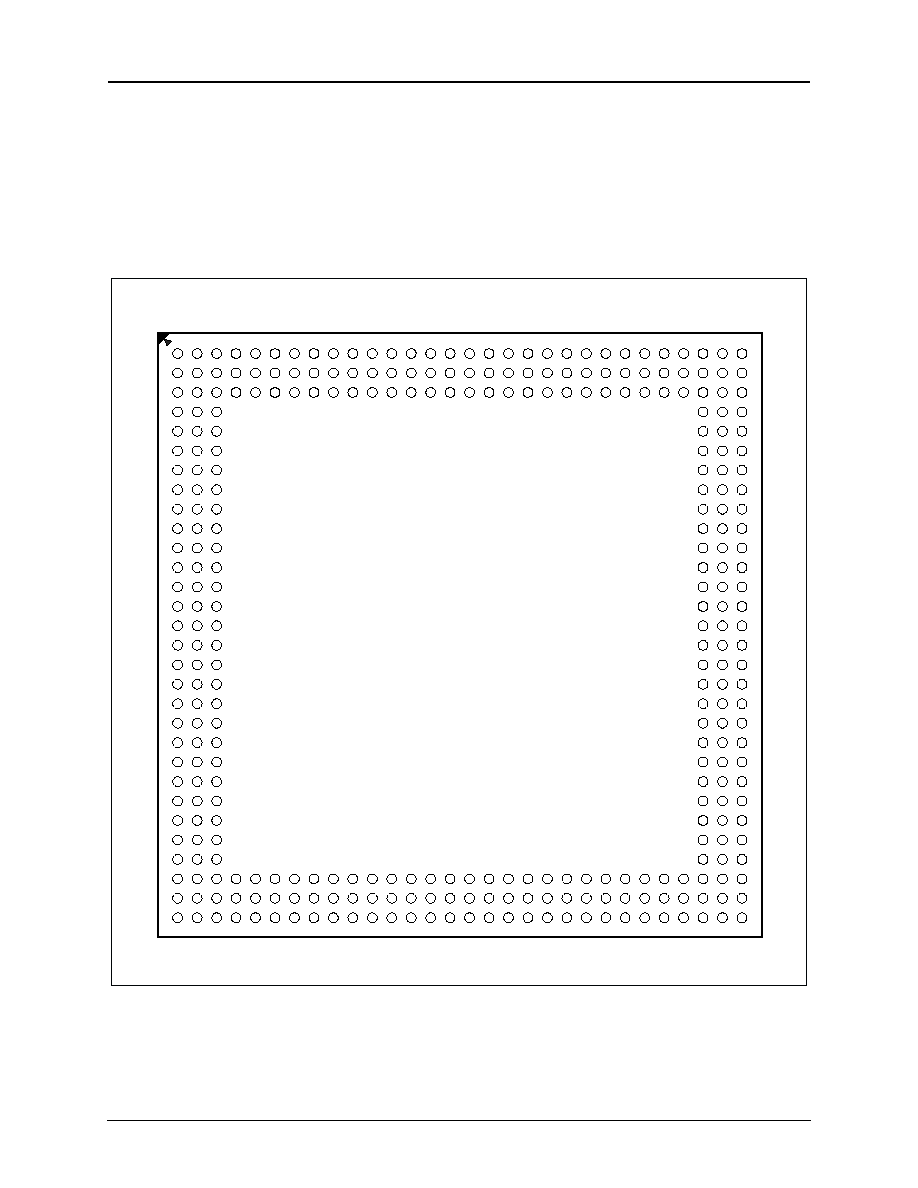
1-12
Mindspeed TechnologiesTM
500238B
Advance Information
Product Description
CX29503 Data Sheet
1.9
Pin Assignments
The CX29503 is packaged in a 324-pin Tape Ball Grid Array (TBGA). A pinout
diagram is provided in
Figure 1-7
. See
Table 1-6
for pin assignments,
Table 1-7
for
pin type definitions, and
Table 1-8
for pin definitions.
Figure 1-7. CX29503 324-pin TBGA Pinout Diagram
10
2
3
4
5
6
7
8
9
1
2
3
4
5
6
7
8
9
1
30
29
28
27
26
25
24
23
22
21
20
19
18
17
16
15
14
13
12
11
10
30
29
28
27
26
25
24
23
22
21
20
19
18
17
16
15
14
13
12
11
A
R
P
N
M
L
K
J
H
G
F
E
D
C
B
AK
AJ
AH
AG
AF
AE
AD
AC
AB
AA
Y
W
V
U
T
A
R
P
N
M
L
K
J
H
G
F
E
D
C
B
AK
AJ
AH
AG
AF
AE
AD
AC
AB
AA
Y
W
V
U
T
CX29503
Top View
100702_008

1-13
Mindspeed TechnologiesTM
500238B
Advance Information
Product Description
CX29503 Data Sheet
Ball
Signal
A1
VGG[0]
A2
VSSC[0]
A3
VSSC[1]
A4
CLK_TXDS3
A5
RESET_N
A6
UNUSED
A7
CK_SRC[0]
A8
TLINECLK[0]
A9
TLINECLK[1]
A10
TLINECLK[2]
A11
TXPOS[0]
A12
TXPOS[1]
A13
TXPOS[2]
A14
TXNEG[0]
A15
TXNEG[1]
A16
TXNEG[2]
A17
VCO[0]
A18
VCO[1]
A19
VCO[2]
A20
UNUSED
A21
CLK_TEST[15]
A22
CLK_TEST[13]
A23
CLK_TEST[11]
A24
CLK_TEST[9]
A25
CLK_TEST[7]
A26
CLK_TEST[5]
A27
CLK_TEST[3]
A28
VSSC[2]
A29
VSSC[3]
A30
VGG[1]
B1
VSSC[4]
B2
VSSC[5]
B3
VSSC[6]
B4
CLK_TXDS1
B5
TRISTATE
B6
SCAN_EN
B7
CK_SRC[1]
B8
RLINECLK[0]
B9
RLINECLK[1]
B10
RLINECLK[2]
B11
RXPOS[0]
B12
RXPOS[1]
B13
RXPOS[2]
B14
RXNEG[0]
B15
RXNEG[1]
B16
RXNEG[2]
B17
RXCKI[0]
B18
RXCKI[1]
B19
RXCKI[2]
B20
CLK_TEST[16]
B21
CLK_TEST[14]
B22
CLK_TEST[12]
B23
CLK_TEST[10]
B24
CLK_TEST[8]
Ball
Signal
B25
CLK_TEST[6]
B26
CLK_TEST[4]
B27
CLK_TEST[2]
B28
VSSC[7]
B29
VSSC[8]
B30
VSSC[9]
C1
VSSC[10]
C2
VSSC[11]
C3
VDDIO[0]
C4
VSSIO[0]
C5
VDDC[0]
C6
VSSC[12]
C7
VDDIO[1]
C8
VSSIO[1]
C9
VDDC[1]
C10
VSSC[13]
C11
VDDIO[2]
C12
VSSIO[2]
C13
VDDC[2]
C14
VSSC[14]
C15
VDDIO[3]
C16
VSSIO[3]
C17
VDDC[3]
C18
VSSC[15]
C19
VDDIO[4]
C20
VSSIO[4]
C21
VDDC[4]
Ball
Signal
Table 1-6. Pin Assignments (1 of 4)

1-14
Mindspeed TechnologiesTM
500238B
Advance Information
Product Description
CX29503 Data Sheet
C22
VSSC[16]
C23
VDDIO[5]
C24
VSSIO[5]
C25
VDDC[5]
C26
VSSC[17]
C27
VDDIO[6]
C28
VSSIO[6]
C29
VSSC[18]
C30
VSSC[19]
D1
CLK_TXE3
D2
CLK_TXE1
D3
VSSC[20]
D28
VDDC[6]
D29
CLK_TEST[0]
D30
CLK_TEST[1]
E1
TDO
E2
TDI
E3
VDDC[7]
E28
VSSC[21]
E29
UNUSED
E30
TSB_CLK[0]
F1
TCK
F2
TMS
F3
VSSIO[8]
F28
VDDIO[7]
F29
TSB_ORSTUFF[0]
F30
TSB_TDAT[0]
Ball
Signal
G1
TRST_N
G2
CLK_1HZ
G3
VDDIO[8]
G28
VSSIO[7]
G29
TSB_ORDAT[0]
G30
TSB_STB[0]
H1
SIB_TXDAT[5]
H2
SIB_TXDAT[6]
H3
VSSC[22]
H28
VDDC[8]
H29
TSB_OTDAT[0]
H30
TSB_TSTUFF[0]
J1
SIB_TXDAT[2]
J2
SIB_TXDAT[7]
J3
VDDC[9]
J28
VSSC[23]
J29
TSB_OTSTUFF[0]
J30
TSB_RDAT[0]
K1
SIB_TXDAT[1]
K2
SIB_TXDAT[4]
K3
VSSIO[10]
K28
VDDIO[9]
K29
TSB_OSTB[0]
K30
TSB_RSTUFF[0]
L1
SIB_RXSTRT[0]
L2
SIB_TXDAT[3]
L3
VDDIO[10]
Ball
Signal
L28
VSSIO[9]
L29
TSB_OCLK[0]
L30
TSB_RSYNC[0]
M1
SIB_TXDAT[0]
M2
SIB_TXPRTY
M3
VSSC[24]
M28
VDDC[10]
M29
TSB_TSYNCO[0]
M30
TSB_TSYNCI[0]
N1
SIB_TXHSCLK
N2
SIB_TXCLK
N3
VDDC[11]
N28
VSSC[25]
N29
TSB_CLK[1]
N30
TSB_ORDAT[1]
P1
SIB_RXSTRT[1]
P2
SIB_TXSTRT
P3
VSSIO[12]
P28
VDDIO[11]
P29
TSB_RDAT[1]
P30
TSB_ORSTUFF[1]
R1
SIB_RXCLK
R2
SIB_RXHSCLK
R3
VDDIO[12]
R28
VSSIO[11]
R29
TSB_TDAT[1]
R30
TSB_OCLK[1]
Ball
Signal
Table 1-6 Pin Assignment (2 of 4)

500238B
Mindspeed TechnologiesTM
1
-
15
Advance Information
CX29503 Data Sheet
T1
SIB_RXDAT[7]
T2
SIB_RXDAT[6]
T3
VSSC[26]
T28
VDDC[12]
T29
TSB_TSTUFF[1]
T30
TSB_OTSTUFF[1]
U1
SIB_RXSTRT[2]
U2
SIB_RXDAT[3]
U3
VDDC[13]
U28
VSSC[27]
U29
TSB_RSTUFF[1]
U30
TSB_OTDAT[1]
V1
SIB_RXDAT[5]
V2
SIB_RXDAT[4]
V3
VSSIO[14]
V28
VDDIO[13]
V29
TSB_STB[1]
V30
TSB_OSTB[1]
W1
SIB_RXPRTY
W2
SIB_RXDAT[0]
W3
VDDIO[14]
W28
VSSIO[13]
W29
TSB_RSYNC[1]
W30
TSB_TSYNCO[1]
Y1
SIB_RXDAT[1]
Y2
SIB_RXDAT[2]
Y3
VSSC[28]
Ball
Signal
Y28
VDDC[14]
Y29
TSB_TSYNCI[1]
Y30
TSB_CLK[2]
AA1
UNUSED
AA2
UNUSED
AA3
VDDC[15]
AA28
VSSC[29]
AA29
TSB_ORDAT[2]
AA30
TSB_RSTUFF[2]
AB1
TSTBUS[0]
AB2
TSTBUS[1]
AB3
VSSIO[16]
AB28
VDDIO[15]
AB29
TSB_ORSTUFF[2]
AB30
TSB_STB[2]
AC1
TSTBUS[2]
AC2
TSTBUS[3]
AC3
VDDIO[16]
AC28
VSSIO[15]
AC29
TSB_OSTB[2]
AC30
TSB_RDAT[2]
AD1
TSTBUS[4]
AD2
TSTBUS[5]
AD3
VSSC[30]
AD28
VDDC[16]
AD29
TSB_OTDAT[2]
AD30
TSB_TDAT[2]
Ball
Signal
AE1
TSTBUS[6]
AE2
TSTBUS[7]
AE3
VDDC[17]
AE28
VSSC[31]
AE29
TSB_OCLK[2]
AE30
TSB_TSTUFF[2]
AF1
TSTBUS[8]
AF2
TSTBUS[9]
AF3
VSSIO[18]
AF28
VDDIO[17]
AF29
TSB_OTSTUFF[2]
AF30
TSB_RSYNC[2]
AG1
TSTBUS[10]
AG2
TSTBUS[11]
AG3
VDDIO[18]
AG28
VSSIO[17]
AG29
TSB_TSYNCO[2]
AG30
TSB_TSYNCI[2]
AH1
VSSC[32]
AH2
VSSC[33]
AH3
VSSC[34]
AH4
VDDC[18]
AH5
VSSC[35]
AH6
VDDIO[19]
AH7
VSSIO[19]
AH8
VDDC[19]
AH9
VSSC[36]
Ball
Signal
Table 1-6 Pin Assignment (3 of 4)

1-16
Mindspeed TechnologiesTM
500238B
Advance Information
Product Description
CX29503 Data Sheet
AH10
VDDIO[20]
AH11
VSSIO[20]
AH12
VDDC[20]
AH13
VSSC[37]
AH14
VDDIO[21]
AH15
VSSIO[21]
AH16
VDDC[21]
AH17
VSSC[38]
AH18
VDDIO[22]
AH19
VSSIO[22]
AH20
VDDC[22]
AH21
VSSC[39]
AH22
VDDIO[23]
AH23
VSSIO[23]
AH24
VDDC[23]
AH25
VSSC[40]
AH26
VDDIO[24]
AH27
VSSIO[24]
AH28
VDDC[24]
AH29
VSSC[41]
AH30
VSSC[42]
AJ1
VSSC[43]
AJ2
VSSC[44]
AJ3
VSSC[45]
AJ4
TSTBUS[13]
AJ5
TSTBUS[15]
AJ6
TSTBUS[17]
Ball
Signal
AJ7
TMODE[1]
AJ8
TMODE[3]
AJ9
DTACK_N
AJ10
CS_N
AJ11
AS_N
AJ12
A[1]
AJ13
A[3]
AJ14
A[5]
AJ15
A[7]
AJ16
A[9]
AJ17
A[11]
AJ18
A[13]
AJ19
A[15]
AJ20
A[17]
AJ21
AD[1]
AJ22
AD[3]
AJ23
AD[5]
AJ24
AD[7]
AJ25
BUS_FMT[1]
AJ26
UNUSED
AJ27
VDDIO[26]
AJ28
VSSC[46]
AJ29
VSSC[47]
AJ30
VSSC[48]
AK1
VGG[2]
AK2
VSSC[49]
AK3
VSSC[50]
Ball
Signal
AK4
TSTBUS[12]
AK5
TSTBUS[14]
AK6
TSTBUS[16]
AK7
TMODE[0]
AK8
TMODE[2]
AK9
INTR_N
AK10
RW_N
AK11
DS_N
AK12
A[0]
AK13
A[2]
AK14
A[4]
AK15
A[6]
AK16
A[8]
AK17
A[10]
AK18
A[12]
AK19
A[14]
AK20
A[16]
AK21
AD[0]
AK22
AD[2]
AK23
AD[4]
AK24
AD[6]
AK25
BUS_FMT[0]
AK26
CLK_860
AK27
VDDIO[25]
AK28
VSSC[51]
AK29
VSSC[52]
AK30
VGG[3]
Ball
Signal
Table 1-6 Pin Assignment (4 of 4)

500238B
Mindspeed TechnologiesTM
1
-
17
Advance Information
CX29503 Data Sheet
Table 1-7. Pin Type Definitions
Symbol
Name and Function
I
Input pin, CMOS levels, no internal termination
IPU
Input pin, CMOS levels, 75 k
internal pull-up
O2
Three-state-capable CMOS output pin; 2 mA drive, 120
equivalent drive impedance
O12
Three-state-capable CMOS output pin; 12 mA drive, 32
equivalent drive impedance
IO12
Three-state-capable CMOS bidirectional pin; 12 mA drive, 32
equivalent drive impedance
ODO
Open drain output; no internal pull up; 12 mA current sink
PC
Digital power pin for core circuits
PI
Digital power pin for I/O pads
PI5
Digital power pin for internal ESD circuits
GC
Digital ground pin for core circuits
GI
Digital ground pin for I/O pads
GENERAL NOTE:
Inputs or Bidirectional pins that act as inputs upon power up must be externally driven to either V
il
or V
ih
levels for correct device
functionality and integrity unless they have internal terminations as indicated in this table.
Table 1-8. Pin Definitions(1 of 6)
Symbol
Reset
(1)
Type
(2)
Signal
Name
Name and Function
JTAG/Scan and Test Access
TCK
--
IPU
--
JTAG Clock--Used to clock-in the TDI and TMS signals and
as a clock-out for the TDO signal.
TRST_N
--
IPU
--
JTAG Reset--An active-low input used to reset the JTAG
logic. IEEE 1149.1 recommends this pin be pulled low in
normal system operation.
TDI
--
IPU
--
JTAG Data Input--The test signal used to receive serial test
instructions and test data.
TMS
--
IPU
--
JTAG Mode Select--The test signal input decoded by the
Test Access Port (TAP) controller to control test operations.
TDO
low
O2
--
JTAG Data Output--The test signal used to transmit serial
test instructions and test data.
TMODE[3:0]
--
I
--
Test Mode--Reserved.
TSTBUS[17:0]
low
O12
--
Test Bus--Reserved.
CLK_TEST[16:0]
--
I
--
Test Port--Test inputs used by Mindspeed for internal test
modes. These inputs should be tied to VSSIO.
SCAN_EN
--
I
--
Scan Enable--Reserved for manufacturing and debug.
Must be connected to ground for normal operation.

1-18
Mindspeed TechnologiesTM
500238B
Advance Information
Product Description
CX29503 Data Sheet
Clock and Control
RESET_N
--
IPU
--
Reset--This is the active-low, system reset signal. This
signal is used as power-up reset.
TRISTATE
--
I
--
Output Three-State Control--When driven high, all output
pins are driven into high impedance state.
CLK_TXDS3
--
I
--
DS3 Transmit Reference Clock-- Reference clock for the
transmit direction. This should be 44.736 MHz ± 20 ppm,
50% ± 5% duty cycle clock. Must be greater than 43.1 MHz
in E3 line side mode to drive the TSB clock (see
Figure 4-3
).
CLK_TXE3
--
I
--
E3 Transmit Reference Clock--Reference clock for the
transmit direction. This should be 34.368 MHz ± 20 ppm,
50% ± 5% duty cycle clock.
CLK_TXDS1
--
I
--
DS1 Transmit Reference Clock--DS1 reference clock for
the transmit direction. This should be a jitter-free clock at
1.544 MHz.
CLK_TXE1
--
I
--
E1 Transmit Reference Clock--E1 reference clock for the
transmit direction. This should be a jitter-free clock at
2.048 MHz.
CLK_1HZ
Z
IO12
--
One-second Timer--If configured as input, this 1 Hz signal
is used to latch error counter values. If configured as
output, the internal 1 Hz time base is brought out on this
pin. This pin is configured as an input by default.
CK_SRC [1:0]
low
I
--
System Interface Select--External pins required to select a
valid system interface (SI-Bus or DS3/E3 Serial) for
CX29503 data and clock operations. A 0x0 or 0x1 signal
selects the SI-Bus as the system interface. A 0x2 or 0x3
selects the DS3/E3 Serial interface as the data source and
allows selection between CLK_TXE3 and CLK_TXDS3 as
the clock source using TXE3_CLKSEL in the Clock
Configuration Register (see
Section 8.8
).
Serial Line Side Interface
TLINECLK[2:0]
low
O2
--
Transmit Line Clock--Provides external indication of the
transmit clock. It is used to clock out the line data signals.
TXPOS[2:0]
low
O2
--
D3/E3 TX Positive Line Data or NRZ Line Data--In Bipolar
mode, positive data is transmitted on this line. For NRZ
mode, NRZ data is transmitted on this line. This signal can
be aligned to either the positive or negative edge of
TLINECK.
TXNEG[2:0]
low
O2
--
D3/E3 TX Negative Line Data or Unused--In Bipolar mode,
negative data is transmitted on this line. In NRZ mode, this
pin is unused and driven low. This signal can be aligned to
either the positive or negative edge of TLINECK.
Table 1-8. Pin Definitions(2 of 6)
Symbol
Reset
(1)
Type
(2)
Signal
Name
Name and Function

500238B
Mindspeed TechnologiesTM
1
-
19
Advance Information
CX29503 Data Sheet
RLINECLK[2:0]
--
I
--
DS3/E3 Line Clock--Clock signal derived from received
data. This should be 44.736 MHz for DS3, 34.368 MHz for
E3, and 51.840 MHz for STS-1.
RXCKI[2:0]
--
I
--
DS3/E3 Dejittered Clock--This signal is to be used in DS3/
E3/STS-1 Line Interface mode. It is used to clock output of
the internal DS3/E3/STS-1 dejitter FIFO. If unused, tie to
ground.
VCO[2:0]
low
O2
--
DS3/E3 Phase Difference Signal--This signal is used by an
external VCO to dejitter the derived line clock.
RXPOS[2:0]
--
I
--
DS3/E3 Positive Data or NRZ Data--In Bipolar mode,
positive data is received via this pin. In NRZ mode, NRZ
data in input on this pin. Inputs are sampled on the
programmable edge of RLINECLK.
RXNEG[2:0]
--
I
--
DS3/E3 Negative Data or LCV Data--In Bipolar mode,
negative data is received via this pin. In NRZ mode, line
code violations are input on this pin. Inputs are sampled on
the programmable edge of RLINECLK.
SI-Bus Interface
SIB_TXHSCLK
--
I
--
SI-Bus High-Speed Transmit Clock--Internal DS3/VT
payload clocks are generated based on this 51.84 MHz
clock.
SIB_TXCLK
--
I
--
SI-Bus Transmit Clock--This clock is used to time all
transmit signals from each mapper/MUX block to the
SONET/SDH MUX device. The nominal clock frequency is
19.44 MHz.
SIB_TXSTRT
--
I
--
SI-Bus Transmit Frame/SPE Alignment signal--This signal
is provided by the SONET/SDH MUX device. It indicates
start of frame or start of SPE depending on the mode of
operation of the SI-Bus. This signal is sampled on the
falling edge of SIBTXCLK.
SIB_TXDAT[7:0]
low
O2
--
SI-Bus Transmit Data--This bus carries the transmit data
from mapper/MUX blocks to the SONET/SDH MUX device.
The data is aligned to the falling edge of SIBTXCLK.
SIB_TXPRTY
low
O2
--
SI-Bus Transmit Data Parity Bit--This bit serves as the odd
parity bit calculated over SIBTXDAT[7:0]. The bit is aligned
to the falling edge of SIBTXCLK.
SIB_RXHSCLK
--
I
--
SI-Bus High Speed Receive Clock--Internal DS3/VT
payload clocks are generated based on this 51.84 MHz
clock.
SIB_RXCLK
--
I
--
SI-Bus Receive Clock--This clock is used to time all receive
signals from the SONET/SDH MUX to the mapper/MUX
blocks. The nominal clock frequency is 19.44 MHz.
Table 1-8. Pin Definitions(3 of 6)
Symbol
Reset
(1)
Type
(2)
Signal
Name
Name and Function

1-20
Mindspeed TechnologiesTM
500238B
Advance Information
Product Description
CX29503 Data Sheet
SIB_RXSTRT [2:0]
--
I
--
SI-Bus Receive Frame/SPE Alignment signal--This signal
is provided by the SONET/SDH MUX. It indicates start of
frame or start of SPE depending on the mode of operation
of the SI-Bus. This signal is sampled on the falling edge of
SIBRXCLK.
SIB_RXDAT[7:0]
--
I
--
SI-Bus Receive Data--This bus carries the receive data
from the SONET/SDH MUX to the mapper/MUX blocks. The
data is sampled on the falling edge of SIBRXCLK.
SIB_RXPRTY
--
I
--
SI-Bus Parity Bit--This bit serves as the odd parity bit
calculated over SIBRXDAT[7:0]. The bit is sampled on the
falling edge of SIBRXCLK.
System Side Interface, Time Slot Bus
TSB_CLK[2:0]
low
OI2
--
Payload Time Slot Bus Clock--This clock is based on
SIB_TXHSCLK or CLK_DS3. It is used for all timing on the
Payload Time Slot bus.
TSB_OCLK[2:0]
low
O2
--
Overhead Time Slot Bus Clock--This clock is a divide-by-4
version of TSB_CLK. It is used for all timing on the
Overhead Time Slot bus.
TSB_TSTUFF [2:0]
low
O2
--
Payload Time Slot Bus Transmit Stuff Indication--When
high, indicates data is not needed eight time slots later.
TSB_OTSTUFF
[2:0]
low
O2
--
Overhead Time Slot Bus Stuff Indication--When high,
indicates data is not needed eight time slots later.
TSB_TSYNC0
[2:0]
low
O2
--
Payload Bus Transmit DS0 Location Indicator from System
Side--When high, this indicates that the first byte of the
first DS0/E0 within the corresponding DS1 is expected on
the transmit payload bus.
TSB_TSYNCI[2:0]
--
I
--
Payload Bus Transmit DS0 Location Indicator to System
Side--When high, this indicates that the current slot
carries the first byte of the first DS0 within the
corresponding DS1 on the transmit payload bus.
TSB_TDAT[2:0]
--
IPU
--
Payload Time Slot Bus Transmit Data--This is the serial
payload data to be transmitted. This signal is sampled in
the rising edge of TSB_TSCLK.
TSB_OTDAT [2:0]
--
IPU
--
Overhead Time Slot Bus Transmit Data--This is the serial
overhead data to be transmitted. This signal is sampled in
the rising edge of TSB_OTSCLK.
TSB_STB[2:0]
low
O2
--
Payload Time Slot Bus Strobe--A strobe signal that
indicates the start of an N time slot frame for payload data,
where N corresponds to the number of Virtual Serial Ports.
TSB_OSTB[2:0]
low
O2
--
Overhead Time Slot Bus Strobe--A strobe signal that
indicates the start of an 84 time slot frame for overhead
data.
Table 1-8. Pin Definitions(4 of 6)
Symbol
Reset
(1)
Type
(2)
Signal
Name
Name and Function

500238B
Mindspeed TechnologiesTM
1
-
21
Advance Information
CX29503 Data Sheet
TSB_RSTUFF [2:0]
low
O2
--
Payload Time Slot Bus Receive Stuff Indication--When
high, indicates that data on TSB_RDAT is not valid data.
Also used in the DS3/E3 Serial Bus mode.
TSB_ORSTUFF
[2:0]
low
O2
--
Overhead Time Slot Bus Receive Stuff Indication--When
high, indicates that data on TSB_ORDAT is not valid data.
TSB_RSYNC[2:0]
low
O2
--
Payload Bus Receive DS0 Location Indicator--When high,
this indicates that the current slot carries the first byte from
the first DS0 in the corresponding DS1
TSB_RDAT[2:0]
low
O2
--
Payload Time Slot Bus Receive Data--This is the received
serial payload data. Also used in the DS3/E3 Serial Bus
mode.
TSB_ORDAT[2:0]
low
02
--
Overhead Time Slot Bus Receive Data--This is the received
serial overhead data.
Microprocessor Interface
BUS_FMT[1:0]
--
I
--
Bus Format Select--In the CX29503, BUS_FMT[1:0] must
be 00 for EBUS bus format.
CS_N
--
I
--
Chip Select--Activates CX29503, and enables MPU read
and write cycles.
AS_N
--
I
--
Address Strobe--Enables the address bus.
The falling edge of AS_N latches the address in CX29503.
DS_N
--
I
--
Read Strobe--Active-low read strobe for read cycles.
RW_N
--
I
--
Write Strobe--Active-low write strobe for write cycles.
DTACK_N
--
ODO
--
Data Transfer Acknowledge--This signal is not used, may
be left unconnected.
INTR_N
--
O
--
Interrupt Request--Open-drain output, which provides a
common interrupt request for all of the interrupt sources in
CX29503.
CLK_860
--
I
--
MPC 860 Clock--This pin should be tied to ground.
AD[7:0]
--
IO12
--
Address/Data Bus--The 8-bit data bus.
A[17:0]
--
I
--
Address Bus--The 18-bit address bus. The AD[7:0] signals
must be externally tied to the A[7:0] signals.
Supply Power
VDDC[24:0]
--
PC
--
Core Logic Power Supply--Voltages for these pins must
conform to the VDD specification in
Table 9-2
.
VDDIO[26:0]
--
PI
--
I/O Pad Power Supply--Voltages for these pins must
conform to the VDDIO specification in
Table 9-2
.
Table 1-8. Pin Definitions(5 of 6)
Symbol
Reset
(1)
Type
(2)
Signal
Name
Name and Function

1-22
Mindspeed TechnologiesTM
500238B
Advance Information
Product Description
CX29503 Data Sheet
VGG[3:0]
--
PI5
--
5 V I/O Pad Power Supply--Voltages for these pins must
conform to the VGG specification in
Table 9-2
.
VSSC[52:0]
--
GC
--
Core Logic Ground--VSSIO and VSSC are shorted together
inside the package via the ground plane. They are shown as
separate pins to identify the corresponding pads on the die.
VSSIO[24:0]
--
GI
--
I/O Pad Ground--VSSIO and VSSC are shorted together
inside the package via the ground plane. They are shown as
separate pins to identify the corresponding pads on the die.
FOOTNOTE:
(1)
Default value after reset.
(2)
See
Table 1-7
for definitions of each type.
Table 1-8. Pin Definitions(6 of 6)
Symbol
Reset
(1)
Type
(2)
Signal
Name
Name and Function

500238B
Mindspeed TechnologiesTM
2
-
1
Advance Information
2.0 Functional Description
2.1
CX29503 Block Diagram
The CX29503 consists of three identical Mapper/Multiplexer (MUX) modules and a
single common interface to the microprocessor, the SI-Bus, and the JTAG test port.
These blocks are laid out on common silicon.
See
Figure 2-1
for a top-level CX29503 block diagram. See
Figure 2-2
for a detailed
block diagram for the Mapper/MUX blocks.

2-2
Mindspeed TechnologiesTM
500238B
Advance Information
Functional Description
CX29503 Data Sheet
Figure 2-1. CX29503 Top-Level Block Diagram
100702_009
MUX/Mapper Block 1
JTAG
LIU #1
LIU #2
STS-12/STS-3
SONET/SDH
Multiplexer
HDLC
Controller Port
HDLC
Controller Port
HDLC
Controller Port
Microcontroller
Complex
SI Bus IN
SI Bus OUT
Serial I/F
CP I/F IN
CP I/F OUT
TSB I/F
MUX/Mapper Block 2
SI Bus IN
SI Bus OUT
Serial I/F
CP I/F IN
CP I/F OUT
TSB I/F
LIU #3
MUX/Mapper Block 3
SI Bus IN
SI Bus OUT
Serial I/F
CP I/F IN
CP I/F OUT
TSB I/F
Top Level MUX (TMX)
SI Bus IN
SI Bus OUT
CP I/F IN
CP I/F OUT
Pad Ring (RNG)
SI Bus I/O
NOTE(S):
1. SI-BUS--SONET Interleaved Bus STS-1 line side interface.
2. TSB--Time Slot Bus system side interface.
3. CP--Control/Microprocessor interface.
4. Serial I/F--Serial line side DS3/E3 interface.
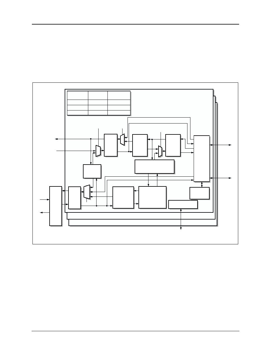
500238B
Mindspeed TechnologiesTM
2
-
3
Advance Information
CX29503 Data Sheet
Functional Description
2.2
CX29503 Detailed Block Diagram
Figure 2-2
illustrates a detailed block diagram. There are three identical Mapper/
MUX blocks within the CX29503.
Figure 2-2
illustrates the major mapping,
MUXing, and framing blocks, and the data paths through them.
Figure 2-2. Mapper/Multiplexer (MUX) Block Diagram
100702_010
DS1/VT1.5, E1/VT2.0,
DS1/VC-11, and E1/VC-12
Tributary Mapper
STS-1 to
VT1.5/2.0
TUG-2/3 to
VC-11/VC-12
MUX
Time Slot
Bus
Interface
Module
Command
and Status
Processor
E-Bus
Processor Interface
28xVT1.5/VC-11
21xVT2.0/VC-12
Overhead
Termination/
Generation
SLICE 2
SLICE 3
Payload
TS-Bus
Overhead
TS-Bus
E-Bus Interface
To Host Processor
(Optional)
SI-Bus
Interface
DS3/E3 Serial
Interface
Unchannelized DS3/E3
Note: CK_SRC[1:0] are hardware pins
Unchannelized STS-1
SI-Bus
I/F
Top-
Level
SI-Bus
MUX
STS-1 to
DS3/E3
Mapper
DS3/E3
Framer
M13 Mode
L3Map[1:0]
CK_SRC[1:0]
RCVR_SEL
2,3
0,1
2,3
0
1
1
0
0
1
M13/E13
MUX
DEMUX
28xDS1
21xE1
Framers
SLICE 1
MUX
Register
Address
Register
Block
M13 Mode
RCVR_SEL
L3Map[1:0]
0x5000
0x01
0x6380
M13/E13
DS1/E1
SONET/SDH

2-4
Mindspeed TechnologiesTM
500238B
Advance Information
Functional Description
CX29503 Data Sheet
2.3
Top-Level MUX
There is one Top-Level MUX block in the CX29503 device. Its function is to provide
a hardware interface between the internal Mapper/MUX blocks and external devices.
This block does not contain any software accessible registers. Its main functions are as
follows:
!
A microprocessor interface
!
A SI-Bus transmit and receive bus interface
!
A JTAG test port interface
2.4
Global Control and Status Block
There are three Global Control and Status blocks for the CX29503, one for each
internal Mapper/MUX block. The main function is to provide top-level status and
control registers for each Mapper/MUX block, mainly the top-level interrupt status
and masking functionality. When an interrupt event from one of the sub-blocks is
reported, the registers in this block allow software to determine the source of the
interrupt. Also, interrupts from individual blocks can be masked at this level.

500238B
Mindspeed TechnologiesTM
2
-
5
Advance Information
CX29503 Data Sheet
Functional Description
2.5
SONET Interleave Bus (SI-Bus)
The SI-Bus interface is capable of full-duplex bidirectional transmission of SONET/
SDH data between a master device and several slave devices.
Figure 2-3
illustrates the basic reference model for the SI-Bus interface and the
information streams between the master and slave devices. The receive data flows
from the master to the slave, and the transmit data flows from the slave to the master.
The clock and marker controls flow from the master to the slave for both transmit and
receive directions.
Figure 2-3. SI-Bus Reference Model
100702_011
Tx Clk
TX
RX
TX
RX
Tx Marker
Tx Data
Rx Clk
Rx Markers
Rx Data
Master
Slave
2-6
Mindspeed TechnologiesTM
500238B
Advance Information
Functional Description
CX29503 Data Sheet
2.5.1
SI-Bus Operation
The SI-Bus operation can be between 3 slave devices (or a multichannel slave device)
and the master and involves the transfer of 3 interleaved STS-1 frames across the data
bus. The Start signals indicate the beginning of the STS-1 frame (A1 octet) and are 1
octet clock in duration. An STS-1 frame is shown in
Figure 2-4
.
Figure 2-4. SI-Bus Unit of Transfer (3 Interleaved STS-1 Frames)
100702_012
270 Columns
125 µs
9 Columns
9
Rows
3 Interleaved
STS-1 Envelopes
Transport
Overhead

500238B
Mindspeed TechnologiesTM
2
-
7
Advance Information
CX29503 Data Sheet
Functional Description
2.5.1.1 Transmit
Interface
The master device generates TxHSClk, TxClk, and TxStart signals to control the slave
devices. The slave devices respond with TxData and TxPrty in their appropriate time
slots. The master device samples TxData and TxPrty on the rising edge of TxClk. The
master device provides TxStart synchronously with the rising edge of TxClk. The data
relationships are shown below in
Figure 2-5
. The master device expects to sample the
A1 octet position (the first octet of the STS frame) on clock edge 2 after the TxStart
signal is provided (edge 1). The master device samples data on every TxClk edge,
with 2,430 clock edges defining the 3 interleaved STS-1 frames. Each slave device
responds on every third TxClk edge and is three-stated during the intervening 2 TxClk
cycles. Each slave has a predetermined time slot in which it is expected to respond
relative to the rising edge of the TxStart signal. The slave device does not have to
generate the correct Transport Overhead, but needs to insert dummy data on these
clock edges. The master device generates the correct Transport Overhead. The content
of the Path Overhead positions is dependent on the master/slave implementations. The
TxPrty signal is not shown but should follow the same relationship as TxData. A
multichannel capable slave does not have to three-state the data bus between channels
and can drive interleaved data continuously onto the bus.
Figure 2-5. SI-Bus Transmit Signal Relationship
100702_013
TxClk
TxStart
TxData[7:0]
from Slave1
TxData[7:0]
from Slave2
TxData[7:0]
from Slave3
1
Payld
756
Payld
756
2
A1
A2
A1
A2
A1
A2
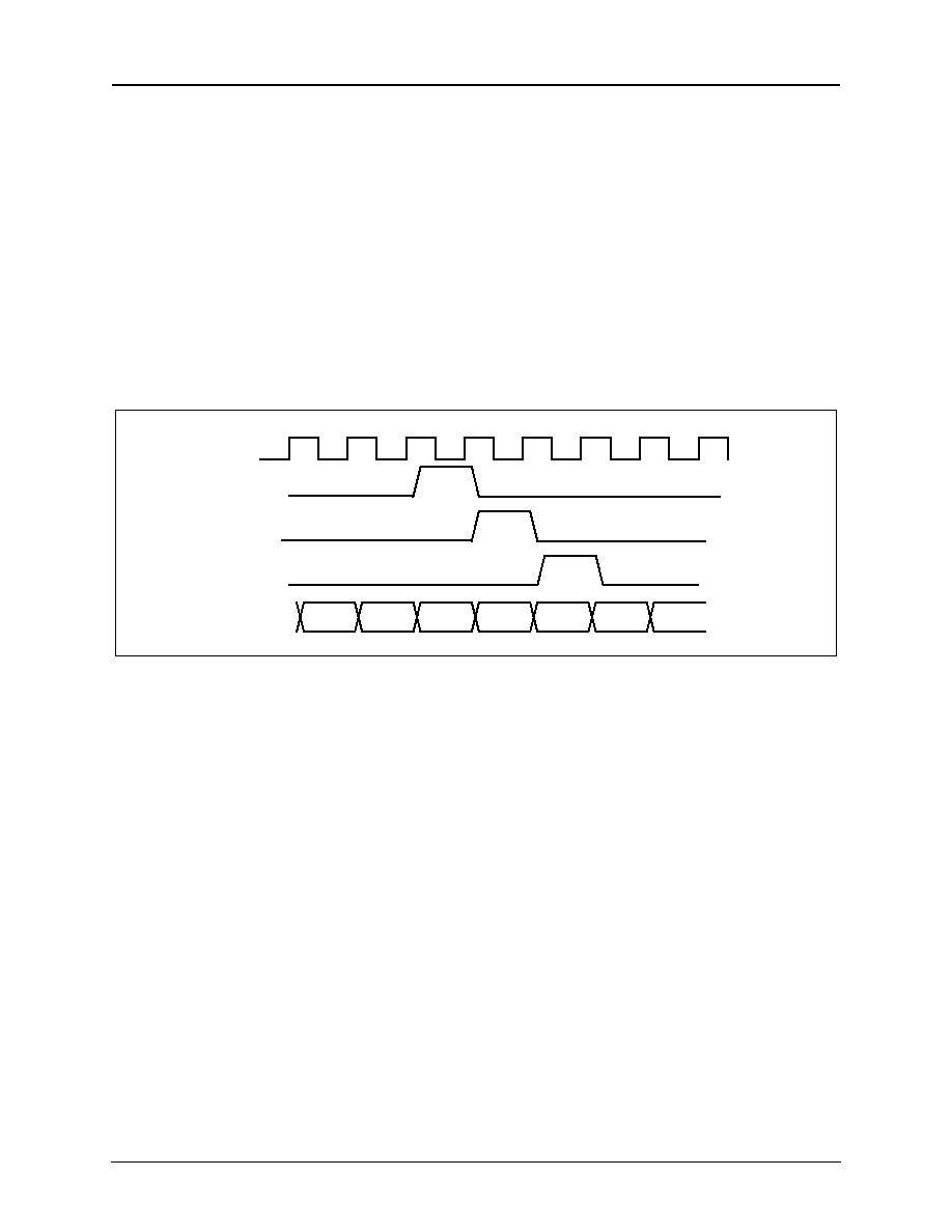
2-8
Mindspeed TechnologiesTM
500238B
Advance Information
Functional Description
CX29503 Data Sheet
2.5.1.2 Receive
Interface
The master device generates RxHSClk, RxClk, RxStart[3:1], and RxData signals to
control the slave devices. The RxStart[3:1] and RxData signals are provided
synchronously with the rising edge of RxClk. The data relationships are shown below
in
Figure 2-6
. Each RxStart signal indicates the position of the A1 octet in the STS-1
frame that corresponds to its number. RxStart[1] indicates the A1 position in STS-1
Frame 1, RxStart[2] indicates the A1 position in STS-1 Frame 2, and RxStart[3]
indicates the A1 position in STS-1 Frame 3. Each slave device samples data on the
falling edge of every third clock relative to the rising edge of its RxStart signal. One
RxClk edge is present for each of the 2,430 octets in the 3 interleaved STS-1 frames.
The RxPrty signal is not shown but has the same relationship as RxData.
Figure 2-6. SI-Bus Receive Signal Relationship
100702_014
RxClk
RxStart[1]
RxStart[2]
RxStart[3]
RxData[7:0]
Payld
756 B
Payld
756 C
A1 A
A1 B
A1 C
A2 A
A2 B

500238B
Mindspeed TechnologiesTM
2
-
9
Advance Information
CX29503 Data Sheet
Functional Description
2.5.2
CX29503 Connection to CX29610
Figure 2-7
illustrates the STS-12/STM-3 connection between 4 CX29503 devices and
1 CX29610 device. The "n" suffixes on the CX29610 signal names range from 1≠4
and indicate the 4 SI-Bus interfaces on the CX29610. The set of signals for each SI-
Bus interface must connect to the same CX29503 device. For example, STxHSClk_1,
STxClk_1, etc. must connect to the same CX29503 device.
Figure 2-7. Interconnection Between CX29503 and CX29610
100702_015
STxHSClk_n
STxClk_n
STxData[7:0]_n
STxPrty_n
STxStart_n
SRxHSClk_n
SRxClk_n
SRxStart[3]_n
SRxStart[2]_n
SRxStart[1]_n
SRxPrty_n
SRxData[7:0]_n
SIB_TXHSCLK
SIB_TXCLK
SIB_TXDAT[7:0]
SIB_TXPRTY
SIB_TXSTRT
SIB_RXHSCLK
SIB_RXCLK
SIB_RXSTRT[2]
SIB_RXSTRT[1]
SIB_RXSTRT[0]
SIB_RXPRTY
SIB_RXDAT[7:0]
CX29610
CX29503

2-10
Mindspeed TechnologiesTM
500238B
Advance Information
Functional Description
CX29503 Data Sheet
2.6
SONET/SDH Mapper/Multiplexer (MUX) Block
The SONET/SDH Mapper/MUX block performs the following functions:
!
Interfacing to the SI-Bus on the line side
!
Interfacing to the DS3/E3 Framer and DS1/E1 framers
!
Interfacing to the TSB block on the system side
!
STS-1 to VT1.5/VT2.0 and VC-3 to VC-11/VC12 multiplexing
!
STS-1 to DS3/E3 mapping and VC-3 to DS3/E3 mapping
!
VT1.5 to DS1 and VT2.0 to E2 mapping; VC-11 to DS1 and VC-12 to E1
mapping
The block is partitioned into the receiver and transmitter sub-blocks. The description
in the following sections emulate that partitioning.

500238B
Mindspeed TechnologiesTM
2
-
11
Advance Information
CX29503 Data Sheet
Functional Description
Figure 2-8. SONET/SDH Mapper/MUX Functional Block Diagram
100702_016
Sync
Sync
VT Overhead
Insertion (x28)
Transmitter
DS1/E1 Mapping
Function (x28)
DS1/E1 Data
DS1/E1 Clock
Tx STS-3 Data
Tx STS-3 Par
Tx Start
Tx Control
Tx Read Data
Tx Intrp/Ctl
Address
Receiver
SI-Bus
Interface
SI-Bus
Interface
STS-1
Frame
Counter
STS-1
Frame
Counter
STS-1 SPE
Extraction
Control
Micro-
Processor
Control/
Status
Micro-
Processor
Control/
Status
VT Extraction
Control
and PM (x28)
DS1/E1 Demapping
Function (x28)
Rx STS-3 Data
Rx STS-3 Par
Rx Start
STS-1 Data Bus
DS1/E1 Data
(Gapped)
DS1/E1 Clock
VT PM Status
Rx Control
Rx Read Data
Rx Intrp/Ctl
Write Data
STS-1
Overhead
Insertion
Time Slot Bus
Interface
Control
Address
Data
DS3/E3
Demapping
Function
DS3/E3
Smoothing
Function
DS3/E3 Data
(Smoothed)
DS3/E3 Clock
DS3/E3 Mapping
Function
DS3/E3 Data
DS3/E3 Clock
Time Slot Bus
Interface
Control
Address
Data

2-12
Mindspeed TechnologiesTM
500238B
Advance Information
Functional Description
CX29503 Data Sheet
2.6.1
SONET/SDH Mapper/MUX Receiver
This section describes the functionality of the SONET/SDH Mapper/MUX receiver.
The receiver terminology relates to the line side.
2.6.1.1
SI-Bus Receiver Interface
SONET/SDH Mapper/MUX receiver interfaces to the line side via the SI-Bus. STS-1
or TUG-3 frames are transported over the SI-Bus from the higher-level MUX device.
The SI-Bus Receiver Interface block is the receiver's physical interface to the SI-Bus.
It strobes receiver control/data from the SI-Bus and generates the internal control and
byte-wide data bus to be used by the receive side. Control and data are strobed on the
falling edge of the 19.44 MHz SI-Bus receiver clock.
2.6.1.2
STS-1/TUG-3 SPE Extraction Control
The STS-1/TUG-3 Synchronous Payload Envelope (SPE) extraction control performs
pointer interpretation which locates and processes the H1/H2 pointer bytes and locates
the first byte in the SPE envelope. It counts the SPE bytes and columns so that it
provides a point of reference to the DS3/E3 Demapping function, VT extraction
control, and TSB Interface blocks. In cases where there is a TU-3 in the SPE payload,
this block provides the additional pointer interpretation required for this level. This
block detects AIS-P, New Data Flags (NDFs), new pointers without NDFs, and count
positive and negative pointer justification operations as well as provide the current
pointer value.
2.6.1.3
DS3/E3 Demapping Function
The DS3/E3 Demapping function demaps an asynchronously mapped DS3/E3 signal
from the payload capacity of an L3 signal residing on the receive side byte-wide data
bus.
The DS3/E3 Demapping function writes 8 bytes of data and 8 bytes of I-bit mask to an
8
◊
16 barrier FIFO at a 6.48 MHz rate. The DS3/E3 demapper reads from the FIFO
and serializes the data and I-bit mask to two 51.84 MHz bit streams where DS3/E3
bits are identified by the I-bit mask stream. This I-bit mask stream is the data enable
used by the DS3/E3 smoothing block.
The DS3/E3 Demapping function is implemented with a barrier FIFO so that the data
transfer between the enabled 19.44 MHz clock domain and the 51.84 MHz clock
domain does not rely on a known phase relationship between the 2 domains. The
FIFO's read/write pointers have a stride of 4 address locations. This stride of 4 is
established through a hardware reset or a software control bit (soft reset).

500238B
Mindspeed TechnologiesTM
2
-
13
Advance Information
CX29503 Data Sheet
Functional Description
2.6.1.4
DS3/E3 Smoothing Function
The DS3/E3 Smoothing function takes a 51.84 MHz bit stream with data enable that
corresponds to a DS3 or an E3 rate. This 51.84 MHz bit stream contains DS3/E3 data
based on their asynchronous mappings in a SONET/SDH signal. The DS3/E3
smoother generates a 51.84 MHz bit stream of redistributed (smoothed) DS3 or E3
data with a gapped data enable.
The data enable stream is used to gap the 51.84 MHz clock to generate a gapped
51.84 MHz clock for the DS3/E3 framers. The gapping requirement is such that
consecutive gaps are not allowed. The gapped 51.84 MHz clock and smoothed data
interface to the embedded DS3/E3 framers.
The DS3/E3 Smoothing function is implemented with a 256
◊
1 FIFO. 128 bits are
allocated due to the maximum number of consecutive non-DS3 or non-E3 bits that
can be encountered and another 128 bits are allocated for pointer adjustments. The
FIFO is initialized at the half-full position.
For the DS3 case, the FIFO is read with the fast gapping sequence until the minimum
threshold is crossed at the end of the sequence. Once the minimum threshold is
crossed, the FIFO is read with the slow gapping sequence until the minimum threshold
is achieved at the end of the sequence. Thereafter, the fast sequence is again be used.
For the E3 case, the FIFO is read with 1 of 3 gapping sequences, according to the
FIFO fill level based on the following at the end of the preceding sequence:
!
fill level has increased (fast sequence)
!
fill level has stayed constant (nominal sequence)
!
fill level has decreased (slow sequence)
An increment/decrement counter tracks the FIFO fill level.
FIFO overflows and underflows are detected. When detected, the overflow/underflow
status is latched for software read, and the FIFO is reset at the half-full position.
2.6.1.5
VT Extraction Control
The VT extraction control performs VT level pointer interpretations on each VT
present in the SPE envelope, which locates and processes the V1/V2 pointer bytes and
locates the first byte in the VT superframe. VT bytes and columns are counted so that
a point of reference is provided to the VT PM, DS1/E1 Demapping functions, and the
TSB Interface blocks.
This block detects new pointers without NDFs, and counts positive and negative
pointer justification operations as well as provides the current pointer value. The
CX29610 device also tracks these pointer operations.
2-14
Mindspeed TechnologiesTM
500238B
Advance Information
Functional Description
CX29503 Data Sheet
2.6.1.6
VT Performance Monitoring
The VT Performance Monitoring (PM) block implements performance monitoring on
the received V5, J2, Z6/N2, and Z7/K4 VT overhead bytes as defined in GR-253 and
G.707. These bytes are reported in the registers listed in
Table 2-1
.
The start and end of the VT-level events are reported in the
Table 2-2
status registers.
An interrupt can be enabled based on the start or end of the event. RFI-V is only
defined for byte-sync DS1 applications that the CX29503 does not support.
Table 2-1. VT Overhead Bytes and Associated Registers
VT Overhead Byte
Register
Signal level field of V5
TXVTLAB
J2 trace buffer--address
TXJ2ADD
J2 trace buffer--data
TXJ2DAT
Z6/N2 byte
TXN2
Z7/K4 byte
TXK4
Table 2-2. VT Start/End Events and Associated Registers
VT Start/End Event
Status Registers
Interrupt Enable Registers
Start
End
Start
End
ERDI-V Payload
RXVSSTAT1
RXVESTAT1
RXVSINTEN1
RXVEINTEN1
ERDI-V Connectivity
RXVSSTAT1
RXVESTAT1
RXVSINTEN1
RXVEINTEN1
ERDI-V Server
RXVSSTAT1
RXVESTAT1
RXVSINTEN1
RXVEINTEN1
RDI-V
RXVSSTAT1
RXVESTAT1
RXVSINTEN1
RXVEINTEN1
PLM-V
RXVSSTAT1
RXVESTAT1
RXVSINTEN1
RXVEINTEN1
UNEQ-V
RXVSSTAT1
RXVESTAT1
RXVSINTEN1
RXVEINTEN1
LOP-V
RXVSSTAT1
RXVESTAT1
RXVSINTEN1
RXVEINTEN1
AIS-V
RXVSSTAT1
RXVESTAT1
RXVSINTEN1
RXVEINTEN1
VT Size Error
RXVSSTAT2
RXVESTAT2
RXVSINTEN2
RXVEINTEN2
RFI-V
RXVSSTAT2
RXVESTAT2
RXVSINTEN2
RXVEINTEN2

500238B
Mindspeed TechnologiesTM
2
-
15
Advance Information
CX29503 Data Sheet
Functional Description
The occurrence of VT "one shot" events are counted in registers and reported in the
Table 2-3
event register. An interrupt can be enabled based on the occurrence of this
event.
2.6.1.7
VT Path Conditioning
This block automatically inserts AIS-V on the downstream VT when AIS-P, AIS-L,
LOP-P or LOF is detected (see
Table 6-1
).
The received BIP2 errors received per frame, AIS-V, LOP-V, UNEQ-V, and PLM-V
are supplied to the transmitter side so that the proper VT overhead generation of REI-
V and RDI-V automatically occurs when enabled (see
Table 6-6
).
2.6.1.8
DS1/E1 Demapping Function
The DS1/E1 Demapping function demaps a bit-asynchronously mapped DS1/E1
signal from the payload capacity of an L1 signal residing on the receive side byte-
wide data bus. The demapping is such that the extracted DS1/E1 is not
desynchronized or smoothed.
The DS1/E1 Demapping function buffers 1 byte of data approximately every 28,
6.48 MHz cycles for a DS1 or approximately every 21, 6.48 MHz cycles for an E1.
The data byte is serialized to an instantaneous rate of 3.24 MHz (8-bits serialized over
16, 6.48 MHz cycles). A gapped 3.24 MHz clock is generated due to bit gapping from
the I-bit mask and byte gapping between the serialized 8-bit data burst.
The gapped 3.24 MHz clock and serialized data interface to the DS1/E1 framers. The
clock/data relationship is such that the data is transmitted on the falling edge of the
clock.
2.6.1.9
Receive Time Slot Bus Interface
The Receive TSB Interface controls clear STS-1 data transfer to the TSB module. See
the TSB description in
Section 2.10.4.3
for details of SONET/SDH channels to TSB
mappings.
Table 2-3. VT One "Shot Events" and Associated Registers
VT "One Shot" Event
Counter Register
Event Register
Interrupt Enable
Register
Low Byte
High Byte
BIP 2 error
BIP2CNTL
BIP2CNTH
RXVEVSTAT
RXVEVINTEN
REI-V error
REIVL
REIVH
RXVEVSTAT
RXVEVINTEN
VT new pointer with or without NDF
--
--
RXVEVSTAT
RXVEVINTEN
Change in J2 trace buffer contents
--
--
RXVEVSTAT
RXVEVINTEN

2-16
Mindspeed TechnologiesTM
500238B
Advance Information
Functional Description
CX29503 Data Sheet
2.6.2
SONET/SDH Mapper/MUX Transmitter
This section describes the SONET/SDH Mapper/MUX block's transmit side
2.6.2.1
SI-Bus Transmitter Interface
The SI-Bus Transmitter interface is the TX physical interface to the SI-Bus. It strobes
TX control from the SI-Bus and generates the internal control to be used by the
transmit side and drives the byte-wide data bus with parity from the transmit side onto
the SI-Bus. Control is strobed on the falling edge and data is driven on the rising edge
of the 19.44 MHz SI-Bus transmitter clock.
2.6.2.2
STS-1/TUG-3 Overhead Insertion
The STS-1/TUG-3 Overhead Insertion block inserts various STS Path Overhead into
either the DS3/E3 Mapped STS-1, VT Mapped STS-1, or Unchannelized STS-1 data
from the TSB interface. This includes a pointer value of 522 (0
◊
20A) into the H1/H2
bytes as well as section and line DCC data bytes, path overhead user channels, and
tandem data link from the TSB. If the TSB interface is the source of the
unchannelized STS-1 data, the necessary stuffing is inserted in the STS-1 frame
structure.
2.6.2.3
VT Build and VT Overhead Insertion
The VT build and VT overhead insertion takes a DS1/E1-mapped VT from the DS1/
E1 Mapping function from the TSB interface and inserts the proper VT overhead in
each VT in the superframe. It generates the proper H4 path overhead byte value. This
VT overhead includes fixed VT pointers, and automatically generates BIP2, REI-V,
and RDI-V when enabled. Other overhead is taken from provisioned registers for the
Signal Label and RFI-V fields in the V5 byte, 16-byte J2 trace, Z6 byte, and Z7 byte.
Various modes of inserting errors on Bit Interleaved Parity-2 bits (BIP-2s) and
Remote Error Indications (REIs) are provided for diagnostic purposes.

500238B
Mindspeed TechnologiesTM
2
-
17
Advance Information
CX29503 Data Sheet
Functional Description
2.6.2.4
DS3/E3 Mapping Function
The DS3/E3 Mapping function asynchronously maps a DS3/E3 signal into the
payload capacity of an L3 signal residing on the transmit-side, byte-wide data bus.
The DS3/E3 Mapping function implements a 96-bit mapping FIFO that is written at a
DS3/E3 rate and read at a gapped STS-1 rate. The FIFO is initialized at the half-full
position.
For the DS3 case, because there is 1 stuff opportunity per frame row, the read
sequence for every row is such that stuffing occurs in that row when the FIFO's fill
level drops below the half-full level at the end of the preceding row. For the E3 case,
because there are 2 stuff opportunities every 3 frame rows, the read sequence for
every 3 rows is because that stuffing occurs in those 3 rows based on the following
after reading the previous three rows:
!
0 bit stuffing: fill level has increased
!
1 bit stuffing: fill level has stayed constant
!
2 bit stuffing: fill level has decreased
Because the write address in the DS3/E3 clock domain needs to be compared to the
read address in the STS-1 clock domain to determine the FIFO fill level, a
synchronization of these addresses needs to occur. A 2-bit counter in the DS3/E3
clock domain generates a 2/3 duty cycle signal (high 2 cycles, low 1 cycle) that is
sampled by the STS-1 clock to indicate that the write address has been incremented
by 3. An increment/decrement counter in the STS-1 clock domain then tracks the
FIFO fill level.
When overflows and underflows are detected, the overflow/underflow status is latched
and the FIFO is reset at the half-full position.
2.6.2.5
DS1/E1 Mapping Function
The DS1/E1 Mapping function asynchronously maps a DS1/E1 signal into the
payload capacity of an L1 signal residing on the transmit-side, byte-wide data bus.
The DS1/E1 Mapping function implements a 112-bit mapping FIFO that is written at
a DS1/E1 rate and read at a 19.44 MHz rate. The FIFO is initialized at the half-full
position. Because there are 2 stuff opportunities per VT/VC superframe, the read
sequence for every superframe is such that stuffing will occur in that superframe
based on the following at the end of the preceding superframe:
!
0 bit stuffing: fill level has increased
!
1 bit stuffing: fill level has stayed constant
!
2 bit stuffing: fill level has decreased
Because the write address in the DS1/E1 clock domain needs to be compared to the
read address in the 19.44 MHz clock domain to determine the FIFO fill level, a
synchronization of these addresses occurs. The DS1/E1 clock is sampled by the
19.44 MHz clock to indicate that the write address has incremented. An increment/
decrement counter in the 19.44 MHz clock domain then tracks the FIFO fill level.
When overflows and underflows are detected, the overflow/underflow status is latched
and the FIFO is reset at the half-full position.

2-18
Mindspeed TechnologiesTM
500238B
Advance Information
Functional Description
CX29503 Data Sheet
2.6.2.6
Transmit Time Slot Bus (TSB) Interface
The Transmit TSB interface controls clear STS-1 data transfer to the TSB module.
See the TSB description in
Section 2.10
for details of SONET/SDH channels to TSB
mappings.
2.6.3
SONET/SDH Transmitter to Receiver Loopback Control
The SONET/SDH Transmitter is looped back to the receiver via the Loopback control
and is provided for diagnostic purposes. When enabled, this block controls the
Receive Start and Transmit Start signals so that the receiver section is in step with the
transmitter section. The transmitter SI-Bus data and parity can then be directly looped
to the receiver SI-Bus data and parity.

500238B
Mindspeed TechnologiesTM
2
-
19
Advance Information
CX29503 Data Sheet
Functional Description
2.7
DS3/E3 Framer Block
The DS3/E3 framing function operates in DS3-mapped STS-1, DS3/E3-mapped VC-
3, or external DS3/E3 access mode. In this operating mode, either the embedded DS1/
E1 can be derived from M13 block or the entire DS3/E3 payload data is terminated at
the TSB module. The DS3/E3 framing detection/insertion, performance monitoring,
alarm generation, overhead bit drop/insert function, and loopback capability are
supported within this block. Additionally, the embedded Terminal Data Link (TDL) is
also terminated at the embedded HDLC controller.
A framer core block diagram is shown in
Figure 2-9
The CX29503 has three DS3/E3 Framer Blocks, one per multiplexing /mapping
module. The DS3/E3 framers operate when the device is configured to one of the
following modes:
!
channelized DS3/E3 where the output is routed to the M13/E13 block
!
unchannelized DS3/E3
!
DS3/E3 mapped STS-1/VC-3
The DS3/E3 framing detection/insertion, performance monitoring, alarm generation,
overhead bit processing, and loopback capability are supported within this block. An
internal HDLC controller terminates the embedded TDL.
A DS3/E3 framer core is compatible with Mindspeed's CX28342/3/4/6/8 DS3/E3
framer device, and software and functionality compatibility is maintained.
The following functions are provided within this block:
Access Control:
!
Selection of receiver data/clock path either from STS/SDH desynchronizer or
external I/O. STS/SDH desynchronizer data path is selected in the default mode.
!
Selection of transmit data path either from M13 or TSB Module. M13 data path is
selected in the default mode.
Dual Rail and NRZ Interface:
!
Dual-rail mode supports B3ZS, HDB3 and AMI line code.
!
In the NRZ mode, negative rail I/O can be used to carry the Line Code Violation
(LCV) information.
!
E3--G.751 framing is supported, G.832 framing is not.
!
The maximum frame-up time for DS3 is 1.5 ms.
!
The maximum frame-up time for E3 is 1.0 ms.
!
Supports Auto-reframe and Forced-reframe modes.
!
Supports the following in frame criteria:
"
DS3--Frame error-free for 3 consecutive frames
"
E3--Frame word error-free for 3 consecutive frames

2-20
Mindspeed TechnologiesTM
500238B
Advance Information
Functional Description
CX29503 Data Sheet
Figure 2-9. DS3/E3 Framer Block Diagram
Encoder
100702_017
RXPOS
RXNEG
LINECK
Decoder
Unipolar
Data
VCO
RXCKI
RX
Dejitter
FIFO
MUX
MUX
{RXFIFEN}
RXDAT
RXMSY
RXGAPCK
REXT
REXTCK
Frame
RECOVERY
Frame/Overhead/
Payload Bit
Check
Status/Event
Indications to
µP Interface
Status Registers
and Counters
FEBE/RAI
Generation
Indication
To Message
Buffer and Status
Register in µP
Interface
RX
Data
Link
RX
FEAC
Channel
To Message Byte
and Status Register
in µP Interface
FEBE/RAI
Generator
{TXALM}
MUX
Payload
Pattern
Generator
TXDATI
TEXT
From Message Buffer
in µP Interface
To Status Register
in µP Interface
From Message Byte
in µP Interface
To Status Register
in µP Interface
TX
Data
Link
TX
FEAC
Channel
TXCKI
TXCLK
Framing
and
Overhead
Insertion
Unipolar
Data
TXPOS
Source
Loopback
Remote Line
Loopback
Shallow
Line
Loopback
TXNEG
TCLKO
Receiver and Transmitter
Performance Monitoring
Status Register End Counters
Microprocessor Interface
TEXTCK
TXSY
TXGAPCK
NOTE(S)
1. { } indicates a programmable control bit.
MUX
MUX
OneSec AD
A ALE RD WR
es DTAOL Intr.
Control
and Status

500238B
Mindspeed TechnologiesTM
2
-
21
Advance Information
CX29503 Data Sheet
Functional Description
DS3/E3 Framer Functionality:
!
DS3/E3 frame format support
"
DS3--M13, M23, and C-parity
!
Supports the following out-of-frame criteria.
"
DS3 mode--3 or more frame bit errors in 16 consecutive F-bits, or at least 1
M-bit error in 2 out of 4 consecutive frames
"
E3 G.751 mode--At least 1 frame word error in 4 consecutive frames.
Performance Monitor:
!
Alarm Detection
"
Loss Of Signal (LOS) detection in the dual-rail interface mode
"
IDLE signal detection in the DS3 mode
"
AIS detection
"
RAI/Remote Defect Indication (RDI) detection
"
Out-Of-Frame (OOF) detection
"
Severely Errored Frame (SEF) detection in the DS3 mode
"
All alarms, except the start of an SEF interrupt event, provide separate
maskable interrupt status for alarm state transition in- and out-state.
!
Performance Monitor Counter Functionality
"
LCV counter
"
Excess 0 counts in the dual-rail interface mode
"
Frame error counts
"
Parity error counts in the DS3 frame format
"
Parity bit disagreement counts in the DS3 frame format
"
Path parity error counts in the DS3 C-Parity frame format
"
FEBE error counts in DS3 C-Parity frame format
"
X-bit disagreement counts in DS3 M13, C-Parity frame format
"
All counters except the LCV counter are 16-bits long and are able to hold 1-
second counts in the presence of a 10
-3
error rate without an overflow. The
LCV counter is 24-bits long and is able to hold every LCV in a 1-second period
without an overflow
"
All counters operate in Real-Time Updating mode and 1-Second Latched mode
"
All counters provide counter overflow status with maskable interrupt capability
Alarm and Error Insertion:
!
AIS signal insertion toward the line side
!
IDLE signal insertion to the line side in the DS3 frame format
!
Supports automatic (in the receiver frame and CP-parity error condition) FEBE
insertion in the DS3 C-parity frame format
!
Supports manual RAI insertion in both DS3 and E3 G.751 frame format. The auto
RAI insertion is also supported in the E3 G.751 frame format during the receiver
OOF or LOS condition
!
Supports single error insertion for LCV (including BPV and illegal substitution),
frame, parity, C-Path Parity bit and RAI/RDI, parity-disagreement, X-bit
disagreement, FEBE event
!
Under software control, supports auto unchannelized all-1s insertion toward the
system side during receiver OOF, LOS, AIS, or DS3 IDLE condition

2-22
Mindspeed TechnologiesTM
500238B
Advance Information
Functional Description
CX29503 Data Sheet
Loopback Functionality:
!
Shallow Line Loopback--The entire line side receiver DS3/E3 data stream (before
the line decoder) is looped back to the transmitter.
!
Remote Line Loopback--The entire line side receiver DS3/E3 data stream (after
the line decoder) is looped back to the transmitter.
!
Source Loopback--The system-side transmitter data is looped back to the
receiver.
Overhead Handler:
!
Supports full-duplex HDLC operation for 28.2 Kbps TDL in DS3 C-Parity frame
format, 22.375 Kbps N-bit in E3 G.751 frame format
"
A separate 128-byte FIFO is used in transmitting and receiving directions to
buffer the message
"
Each FIFO is capable of holding multiple messages
"
The Receiver FIFO near-full threshold can be configured in single byte
granularity
"
The Transmit FIFO near-empty threshold can be configured in single byte
granularity
"
The Receive FIFO provides message received status and FIFO near full and
overrun status
"
Transmit FIFO provides message transmitted status and FIFO underrun, empty,
near empty and full status
"
Maskable interrupts are available for the transmitter FIFO near-empty, FIFO
underrun, message transmitted event and receiver FIFO near-full, and FIFO
overrun and message received event
!
Far-End Alarm Control (FEAC) handler
"
Programmable code word transmission operates in single and repetitive code
word mode
"
Single code word mode--interrupt is generated on each 16-bit code word
transmits (1.7 ms)
"
Repetitive code word mode--interrupt is generated on every 10 repetitive code
word transmits
"
Code word detection supports single and 9 out of 10 repetitions modes; under
the worst-case condition, buffer overrun occurs in 1.7 ms for single detection
or 17 ms for the repetitive detection mode
"
A 3-byte deep FEAC stack is also provided for holding the detected code
words; the worst-case takes approximately 68 ms to cause the stack overrun in
9 out of 10 repetitive detection modes.
!
Supports transmitting and receiving of Application Identification Channel (AIC)
messages in DS3 C-parity and DS3-M13 frame format

500238B
Mindspeed TechnologiesTM
2
-
23
Advance Information
CX29503 Data Sheet
Functional Description
2.8
DS1/E1 Framer Block
The CX29503 has 84 DS1/E1 Framer blocks; there are 28 DS1/E1 Framer blocks per
Mapping/MUXing module. DS1/E1 framers operate when the device is configured to
one of the following modes:
!
Channelized DS3/E3
!
DS1/E1 mapped VT/VC
In these modes, 28 DS1 or up to 21 E1 payloads and overhead data can be terminated
at the TSB Interface module for transmission to an external HDLC controller. DS1/E1
framing detection/insertion, performance monitoring, alarm generation, overhead bit
processing, loopback capability, and unchannelized DS1/E1 testing are supported
within this block.
The DS1/E1 framer core is shown in
Figure 2-10
. Because the core is compatible with
Mindspeed's CN8398 DS1/E1 framer device, software and functional compatibility is
maintained.
Figure 2-10. DS1/E1 Framer Core Block Diagram
RDATAO
RDLO
TDLI
RDLCKO
TDLCKO
TXCAT1
RFSYNC
EXT_DSICLK
EXT_E1CLK
TXCLKO
TFSYNC
RPOS
Line
Loopback
Path
Local
Frame
Loopback
Path
RCLKI
TPOS
100702_018
Off-Line
Framer
Framing
Insertion
Alarm
Insertion
BOP
Transmitter
MOP/BOP
Arbitration
AIS
Insertion
Loop Code
PRBS
Detection
Loop Code
PRBS
Detection
Transmitter
Data Link
Controller
Overhead
Data
Insertion
Receiver
BOP
Handler
Receiver
Data LInk
Controller
Overhead
Data
Extraction
Payload
Loopback
FIFO
Performance
Monitor
Receiver
Time Base
Transmitter
Time Base

2-24
Mindspeed TechnologiesTM
500238B
Advance Information
Functional Description
CX29503 Data Sheet
2.8.1
Module Functions
The following functions are provided within the DS1/E1 Framer block:
Access Control:
!
Global selection of line side receiving data along with its clock from the M13 or
VT/VC block. The VT/VC path is selected in the default mode.
!
Drop and insert of any DS1/E1 data, including ESF FDL or E1 Sa4 bits to and
from the TSB module.
DS1/E1 Receive Framer:
!
The framing function is supported using both off-line and on-line framers. The off-
line framer recovers frame alignment. The on-line framer monitors frame error and
OOF conditions.
!
Configurable through software to support auto-reframe and forced reframe mode.
!
Supports the in-frame and out-of-frame criteria listed in
Tables 2-4
and
2-5
.
!
The maximum reframe time is less than 50 ms.
Table 2-4. DS1 Mode In-Frame and Out-of-Frame Criteria
Frame Mode
In-Frame Criteria
Out-of-Frame Criteria
Ft
12 consecutive 1010 patterns are found in an alternate
F-bit location
2 out of 4, 2 out of 5, or 2 out of 6 Ft errors
SF
Valid Ft patterns and 001110 are found in Fs bit
locations
2 out of 4, 2 out of 5, or 2 out of 6 Ft or Fs errors
SF with JYEL
Valid Ft patterns and 00111x are found in Fs bit
locations
2 out of 4, 2 out of 5, or 2 out of 6 Ft or Fs errors
ESF
No CRC mode: valid FPS pattern
CRC mode: valid FPS with correct CRC
2 out of 4, 2 out of 5, or 2 out of 6 FPS errors
Table 2-5. E1 Mode In-Frame and Out-of-Frame Criteria
Frame Mode
In-Frame Criteria
Out-of-Frame Criteria
FAS-only
Valid FAS pattern present only in every other frame
3 consecutive FAS in error
FAS + CRC
2 consecutive valid MFAS patterns (001011xx
sequence within bit 1 of NFAS frame) within 8 ms of
the FAS frame have been located
3 consecutive FAS in error or 915 out of 1,000 CRC
errors

500238B
Mindspeed TechnologiesTM
2
-
25
Advance Information
CX29503 Data Sheet
Functional Description
DS1/E1 Transmit Framer:
!
Supports the following framing pattern:
"
E1 modes supported--FAS-only and FAS + MFAS (CRC4) mode.
Channel Associated Signaling (CAS) mode is not supported.
"
DS1 modes supported--SF and ESF.
SLC-96 and T1DM frame formats are not supported.
Performance Monitoring:
!
RLOF detection--LOF failure detection is supported in the DS1 mode
!
AIS detection
!
RAI detection--Support both yellow alarm (RYEL) and multiframe yellow alarm
(RMYEL) in the real-time and integration modes
"
PM Counters function
≠ Support Frame, CRC, FEBE, LOF, SEF, and COFA error counts
≠ All error counters operate in real-time updating mode and 1-second latched
mode
≠ Frame, CRC, and FEBE counters are capable of holding over 1 second of
errors without overflow
"
All alarms and PM counter overflow events provide maskable interrupt
capability
Alarm and Error Insertion:
!
Supports manual AIS insertion toward the line side
!
Supports manual and automatic (in the Receiver CRC error condition) FEBE
insertion toward the line side
!
Supports manual and automatic (in the RLOF condition) insertion of RAI toward
the line side
"
In the Extended Superframe (ESF) auto-RAI mode, the yellow alarm code
word can be transmitted through the embedded FDL channel
!
Supports auto-AIS insertion to the system side, under software control, during an
OOF condition
!
Supports the insertion of a single frame, COFA, or CRC error
Loopback Capability:
!
Supports programmable 4- to 7-bit in-band loop code transmission and detection
!
Supports out-of-band ESF loop code transmission and detection via the Bit-
Oriented Protocol handler
!
Loopback modes supported
"
Remote Line loopback--The entire line-side receiving data is looped back to
the transmitter. In this mode, the receive clock is used to drive the transmitter.
"
Payload loopback--Only the line-side receiving payload data is looped back to
the transmitter, overhead data is continuously sourced from the transmitter.
Because the transmitted data is driven by the transmit clock, the received
payload data passes through a 64-bit FIFO to accommodate the receiver jitter
(mainly introduced from the VT/VC mapper). The slip status is provided to
indicate a FIFO underflow or overflow condition. This status operates in reset-
on-read modes.
"
Local Framer loopback--The entire transmitted data is looped back to the
receiver.

2-26
Mindspeed TechnologiesTM
500238B
Advance Information
Functional Description
CX29503 Data Sheet
Data Link Channel Handler:
!
Supports the full duplex data link layer operation for the ESF Facility Data Link
(FDL) and E1 Sa4 data link
"
Two separate 64-byte FIFOs are used for the transmit and receive directions for
buffering the messages
"
Each FIFO is capable of holding multiple messages
"
The Receiver FIFO near full threshold can be configured in single byte
granularity
"
The Transmit FIFO near empty threshold can be configured in single byte
granularity
"
The Receive FIFO provides message receiving status, message length and
FIFO empty, near full, and full status
"
The Transmit FIFO provides message transmitting status, and FIFO empty,
near empty, and full status
"
All transmit and receive FIFO statuses have maskable interrupt capability
"
Supports auto-PRM transmission for every 1 second with programmable CR,
R, U1, U2, and SL control bits
"
Both transmit and receive FIFOs are configurable to operate in HDLC mode,
and 6- and 8-bit transparent mode
"
In the transparent mode, the transmit FIFO can be configured as a circular
buffer to allow data to be sent repetitively
!
Bit-Oriented Protocol Handler
"
Supports ESF bit-patterned message transmitting and receiving through the
embedded FDL channel. Includes the following:
≠ Programmable code word transmission with single, 10 repetition, 25
repetition, or continuous modes
≠ Code word detection supports single, 10 repetition, and 25 repetition mode.
"
In the E1 mode, Sa4, Sa5, Sa6, Sa7, and Sa8 can be transmitted and received
through its dedicated 8-bit buffer
!
External Data Link Interface
"
Drop and insert of ESF FDL and E1 Sa4 data link to/from external HDLC
controller
"
Arbitration between external Message-Oriented Protocol (MOP) insertion
(from HDLC controller) and internal Bit-Oriented Protocol (BOP) insertion
(within the Framer)
≠ The Transmitting of MOP has a higher priority
≠ The Framer core is responsible for inserting 27 bytes of the opening flag
and 1 the byte of closing flag for each MOP message
≠ The Transmitting of BOP during data link channel idle or inactive states
!
Processing is performed by hardware; no processing by the CSP or host processor
is required

500238B
Mindspeed TechnologiesTM
2
-
27
Advance Information
CX29503 Data Sheet
Functional Description
DS1/E1 Testing Capability:
!
Programmable pseudo-random pattern generator including 2
11
≠1, 2
15
≠1, 2
20
≠1, and
2
23
≠1 patterns with the option of 7 or 14 zero limit, and data inversion capabilities
!
Single bit error insertion through software control
!
The Error counter is capable of holding up to 4,095 bit errors (> 10
-2
BER) in a 1-
second period
Clock Distribution:
!
Transmit clock selection between external DS1 reference timing source, external
E1 reference timing source, and receiver loop timing
!
Instead of using the system clock as the timing reference, the transmitter and
receiver blocks can use their own clock sources.

2-28
Mindspeed TechnologiesTM
500238B
Advance Information
Functional Description
CX29503 Data Sheet
2.9
M13/E13 Multiplexer (MUX) Block
The M13/E13 MUX block is used to multiplex and demultiplex 28 DS1signals to a
DS3 signal in the North American digital telephony hierarchy and 16 E1 signals to an
E3 signal in the European digital telephony hierarchy. Also, the multiplexing of 21 E1
signals into a DS3 signal is supported per the G.747 standard. A combination of DS1
and E1 signals can be multiplexed into a DS3 as long as the same type of lower rate
(DS1/E1) signals are multiplexed into a single DS2.
Figure 2-11
illustrates the M13/
E13 MUX block.
The M13/E13 block interfaces to the DS3/E3 framer on its line side and to the DS1/
E1 Framer block on its system side. Also, a mode is provided where the
unchannelized DS3/E3 interfaces directly to the TSB on the system side.
The M13/E13 block is capable of operating in 3 different modes. Mode selection is
controlled by the software register setting. Each mode is distinct and mutually
exclusive, i.e, the block can operate in only 1 mode at any given time. The 3 modes are
as follows:
1. M13--Two-stage multiplexing/demultiplexing is implemented. Four DS1 or 3
E1 signals are multiplexed/demultiplexed into 1 DS2 signal. Seven such DS2
signals are multiplexed into/from 1 DS3 signal.
2. E13--Two-stage multiplexing/demultiplexing is implemented. Sixteen E1
signals are multiplexed/demultiplexed into/from 4 E2 signals which are then
multiplexed into/from 1 E3 signal.
3. Unchannelized bypass--In this mode, the multiplexer is bypassed and an
Unchannelized DS3/E3 from the framer is forwarded to the TSB.
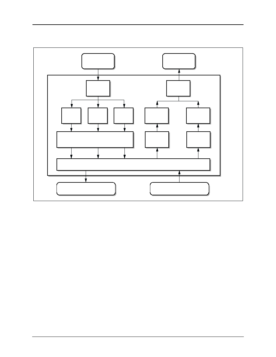
500238B
Mindspeed TechnologiesTM
2
-
29
Advance Information
CX29503 Data Sheet
Functional Description
Figure 2-11. M13/E13 Functional Block Diagram
E23/M23
DEMUX
4 x E2/E1
Framers
7 x DS2/
DS1
Framers
M12/E12 DEMUX
Signal MUX
16 E1 Signals
28 DS1 Signals
4 E2 Signals
7 DS2 Signals
E23/M23
MUX
4 x E2
Framer
7 x DS2
Framer
E12 MUX +
12-Bit/Ch
FIFO
M12/
G.747
MUX + 12-
Bit/Ch FIFO
16 E1 Signals
28 DS1 or 21
E1 Signals
4 E2 Signals
7 DS2 Signals
DS3/E3
from Framer
DS3/E3
to Framer
28 DS1 or 21 E1 or 16 E1 signals
or combination of DS1/E1 signals
28 DS1 or 21 E1 or 16 E1 signals
or combination of DS1/E1 signals
7 x DS2/
E1
Framers
7 DS2 Signals
21 E1 Signals
100702_019

2-30
Mindspeed TechnologiesTM
500238B
Advance Information
Functional Description
CX29503 Data Sheet
2.9.1
Operational Features Specification
The M13/E13 block provides the following features:
Framing:
!
Interfaces to the internal DS3/E3 framer block on the system side
!
Includes seven DS2 and four E2 framers
"
Supports forced reframe for DS2/E2 framers.
"
DS2 average reframe time less than 6 ms for DS1-mapped DS2 and less than 1
ms for E1-mapped DS2 at a Bit Error Rate (BER) of 10
-3
.
"
E2 average reframe time per G.742, section 4.2.
"
DS2 OOF indication algorithm is software selectable between the F-bit only
and the F- and M-bits combined.
"
Software controlled inversion of the second and the fourth DS1 streams per
ANSI T1.107.
"
DS2/E2 AIS detection at a BER of 10
-3
.
"
DS2/E2 OOF, RAI, Loss Of Signal (LOS) and framing error detection and
reporting.
"
DS2 extraction of the DS2 X-bit or G.747 Remote Alarm bit and indication of
far-end receive failure.
"
DS2 performance monitor counters with 1-second latch capability. The
counters are wide enough to accommodate 1 second of data without saturation
at BER levels less than 10
-3
. The counters include: M-bit errors (8-bit), F-bit
errors (8-bit), Loss of Frame (LOF)(8-bit), G.747 Framing Byte (8-bit), G.747
Parity errors (13-bit).
"
E2 reporting of Alarm Indication Bit (AIB) (bit-11), and National Use bit (bit-
12).
"
E2 performance monitor counters with 1-second latch capability. The counters
are wide enough to accommodate 1 second of data without saturation at BER
levels less than 10
-3
. The counters include: Frame Alignment error (8-bit),
LOF (8-bit).
!
Interfaces to the internal DS1/E1 framer blocks on the line side.
Multiplex/Demultiplex Features:
!
Two stage, plesiosynchronous multiplexing of DS1s into a DS2
"
28 DS1s multiplexed into 7 DS2s (4 DS1s into a 1 DS2)
"
Seven DS2s multiplexed into a DS3
!
Two stage, plesiosynchronous multiplexing of E1s into an E3
"
Sixteen E1s multiplexed into 4 E2s (4 E1s into a 1 E2)
"
Four E2s multiplexed into an E3
!
Two stage, plesiosynchronous multiplexing of E1s into a DS3 per G.747 standard
"
Up to 21 E1s multiplexed into 7 DS2s (3 E1s into a 1 DS2)
"
Seven DS2s multiplexed into a DS3
≠ A combination of E1- or DS1-multiplexed DS2s can be multiplexed into a
DS3, but a single DS2 must contain only DS1s or E1s.

500238B
Mindspeed TechnologiesTM
2
-
31
Advance Information
CX29503 Data Sheet
Functional Description
2.10
Time Slot Bus (TSB) Interface
The CX29503 has three TSB Interfaces (see
Figure 2-12
).
The TSB interface provides for full duplex communication with external devices,
such as Mindspeed's CX28500 HDLC controller, over two serial (1-bit wide) buses.
One bus, called the Payload TSB, carries payload data to and from the PDH framers
and SONET/SDH block. The other bus, called the Overhead TSB, carries overhead
data communication channels to and from the PDH framers and SONET/SDH block,
and it carries a device's register content and command data passed between the
Command and Status Processor (CSP) and the local host processor.
Figure 2-12. CX29503 Time Slot Bus Interface
Mapper/MUX
Block 3
CX29503
External Device
TS-Bus
Mapper/MUX
Block 1
Mapper/MUX
Block 2
Payload TS-Bus
Overhead TS-Bus
Payload TS-Bus
Overhead TS-Bus
Payload TS-Bus
Overhead TS-Bus
TS-Bus
TS-Bus
100702_020

2-32
Mindspeed TechnologiesTM
500238B
Advance Information
Functional Description
CX29503 Data Sheet
Figure 2-13
shows the TSB Interface block diagram.
Figure 2-13. TSB Interface Block Diagram
1
Command and Status
Processor (CSP)
TS Bus
SONET/SDH 12.96 Mbps
Serial DS3 11.184 Mbps
PAYLOAD DATA PATHS
OVERHEAD
COMMUNICATION
CHANNELS
OVERHEAD
Unchannelized
STS-1
MUX
DS1
28x
DS1/E1
FRAMERS
E1
28 x RXFIFO
28 x TXFIFO
TDM
MUX
TDM
MUX
DS3/E3
TDL
DCCM
F2
DS1(FDL)/
E1(Sa)
Time Slot Bus
Module
DCCR
F3
K3
N1
SONET
SDH
Mappers
PAYLOAD
38 x RXFIFO
38 x TXFIFO
K4
28
1
1
1
1
1
1
SONET/SDH
Parallel
Payload/OH
Interface
DS1/E1 Serial
Interface
21/16
28
Unchannelized
DS3/E3
1x
DS3/E3
FRAMER
1
1
1 x RXFIFO
1 x TXFIFO
S
T
S
-
1
/
V
C
-
4
VC-11
VC-12
F2
F3
K3
N1
1
1
1
1
V
C
-
3
28
Number of
Channels
28 x RXFIFO
28 xTXFIFO
28
STS-1 to
DS3/E3
Mapper
DS3/E3
Serial
Interface
TS Bus
SONET/SDH 51.84 Mbps
Serial DS3 44.736 Mbps
500238B
Mindspeed TechnologiesTM
2
-
33
Advance Information
CX29503 Data Sheet
Functional Description
The CX29503 serves as the timing master for the TSB Interface and provides clocks
and alignment/marker signals (strobes) to the external device connected via this
interface. The external device provides and accepts data to and from the CX29503
under direction of the clock and control signals provided by the CX29503.
See
Table 2-6
the TSB bandwidths for different line rates. The CX29503 derives the
Payload TSB transmit and receive clocks from the same clock source. The clock
source for the TSB is listed in
Table 4-10
.
2.10.1
Summary of Payload TSB
The Payload TSB provides full duplex operation at one of the three data rates listed in
Table 2-6
. The data on the Payload TSB is framed and consists of 84 time slots per
frame structured as shown in
Figure 2-14
. The CX29503 generates transmit and
receive strobes to mark the first bit of each transmit and receive TSB frame.
Table 2-6. TSB Bandwidths
Line Interface
Payload
TSB Bandwidth
(Mbps ± 20 ppm)
Overhead
TSB Bandwidth
(Mbps ± 20 ppm)
SONET/SDH 51.840
12.960
Serial DS3
44.736
11.184
Serial E3
34.368
8.592
Figure 2-14. TSB Payload Time Slot Diagram
1
2
3
4
1
2
3
5
6
7
8
4
5
6
. . .
79 80 81 82 83 84
1 Byte per Time Slot
Payload TSB Frame = 84 Time Slots
Time Slot No. 1 is first byte of
Payload TSB Frame
Time Slot No. 84 is last byte of
Payload TSB Frame
100702_022
2-34
Mindspeed TechnologiesTM
500238B
Advance Information
Functional Description
CX29503 Data Sheet
2.10.2
Summary of Overhead TSB
The Overhead TSB provides full duplex operation at one-fourth the speed of the
Payload TSB where the same clock source is used to drive both the Transmit and
Receive Overhead TSB clocks.
The data on the Overhead TSB is framed and consists of 84 time slots per frame
structured as shown in
Figure 2-15
. The CX29503 generates transmit and receive
strobes to mark the first bit of each Transmit and Receive TSB frame.
Figure 2-15. TSB Overhead Time Slot Diagram
100702_023
1
2
3
4
5
6
7
8
. . .
1 Time Slot = 1 Byte
Overhead TSB Frame = 84 Time Slots
84
83
82
3
2
1
4
5
Time Slot No. 1 is the 1st byte of
the Overhead TSB Frame
Time Slot No. 84 is the last byte of
the Overhead TSB Frame

500238B
Mindspeed TechnologiesTM
2
-
35
Advance Information
CX29503 Data Sheet
Functional Description
2.10.3
TSB Signals
Figure 2-16
illustrates the TSB connections between the CX29503 and an external
device. The Payload and Overhead buses each have separate Transmit and Receive
paths. The Receive path is defined from the CX29503 to an external device, and the
Transmit path is defined from an external device to the CX29503. The CX29503, as
the bus master, supplies the bus strobes, clocks, and stuff signals.
The requirement for stuffed data is explained in
Section 2.10.4.2
and
Section 2.10.5.2
.
See
Figures 2-18
and
2-21
for the timing diagrams for the stuffing signals,
TSB_TSTUFF and TSB_RSTUFF.
The three sync signals, TSB_TSYNCO, TSB_TSYNCI, and TSB_RSYNC, mark the
first DS0 byte of every DS1 frame. The DS0 byte for TSB_TDAT can either be
marked by the CX29503 using the sync output signal, TSB_TSYNCO, or marked by
the external device using the sync input signal, TSB_TSYNCI. Timing diagrams for
the sync signals, TSB_TSYNCO, TSB_TSYNCI, and TSB_RSYNC are given in
Chapter 1.0
.
Figure 2-16. TSB Interface Pins
CX29503
CX28560
TSB_CLK
TSB_TSTUFF
TSB_TDAT
TSB_RSTUFF
TSB_RDAT
TSB_STB
TSB_OTSTUFF
TSB_OTDAT
TSB_OSTB
TSB_ORSTUFF
TSB_ORDAT
TSB_TSTUFF
TSB_TDAT
TSB_STB
TSB_RSTUFF
TSB_RDAT
TSB_TCLK
TSB_RCLK
TSB_TSTUFF
TSB_TDAT
TSB_STB
TSB_RSTUFF
TSB_RDAT
TSB_TCLK
TSB_RCLK
TSB_OCLK
51.84/44.736/34.368 MHz
12.96/11.184/8.592 MHz
TSB_TSYNCO
TGSYNC
TSB_TSYNCI
TSB_RSYNC
RGSYNC
Diagnostic
Overhead
Payload
Overhead
Payload
NOTE(S):
CX28560 requires pull-up resistors (10 k
on TSB_TDAT and TSB_OTDAT.
100702_024

2-36
Mindspeed TechnologiesTM
500238B
Advance Information
Functional Description
CX29503 Data Sheet
2.10.4
Details of Payload TSB
2.10.4.1
Data Path Signals
The Payload TSB frame can be configured to transport payload data for any of the
following signal types: DS1, E1, unchannelized DS3, unchannelized E3, and
unchannelized STS-1. The Payload TSB can also be configured to carry the payload
from a mix of DS1 and E1 signals.
2.10.4.2 S
tuff Byte Compensation
Stuff bytes are inserted into the Payload TSB to compensate for differences in the data
rate of the TSB and the data rate of the data carried on the bus in both the transmit and
receive directions.
In general, the CX29503 asserts the transmit and the receive stuff signals to initiate or
mark the insertion of stuff bytes into Payload TSB frames to compensate for data rate
offsets that exist between the TSB bandwidth and the bandwidth of the payload
carried on the bus.
Table 2-7
summarizes the bus rates for each type of transport signal format. The TSB
bus rate is based on either the DS3, E3, or SONET line rates. When running at the
TSB bus rate of 51.840 Mbps, stuff bytes are added to the TSB Interface.
Section 2.10.6.1
gives timing diagrams for the transmit stuffing signal,
TSB_TSTUFF, and the receive stuffing signal, TSB_RSTUFF, respectively.
Table 2-7. TSB Data Paths and Bus Rates
(1)
Line Interface
TSB Signal Type
Payload TSB
Bus Rate
(Mbps)
Overhead TSB
Bus Rate
(Mbps)
1
Serial DS3
unchannelized DS3
44.736
11.184
2
Serial DS3
28
◊
DS1
44.736
11.184
3
Serial DS3
21
◊
E1
44.736
11.184
4
Serial DS3
mixed DS1/E1
44.736
11.184
5
Serial E3
unchannelized E3
44.736
11.184
6
Serial E3
16
◊
E1
44.736
11.184
7
SONET/SDH
Note
(2)
51.840
12.96
FOOTNOTE:
(1)
The numbers in this column are used for reference purposes (see
Table 4-10
).
(2)
Unchannelized STS-1, unchannelized DS3, unchannelized E3, 28 x DS1, 21 x E1, 16 x E1, mixed DS1/E1.

500238B
Mindspeed TechnologiesTM
2
-
37
Advance Information
CX29503 Data Sheet
Functional Description
2.10.4.3
Mapping of Payload to TSB Payload Time Slots
The Payload TSB transports up to 28 independent data paths. Each data path in both
the transmit and receive directions is transported over a set of multiple time slots
within each Payload TSB frame. At either end of the Payload TSB, each multiple set
of time slots is concatenated into a Virtual Serial Port (VSP) that corresponds to its
respective data path. This provides full-duplex communication for each data path
across the bus.
Mapping of Digital Level 1 Signals
In general, data passed through each digital level 1 framer/mapper is mapped to/from
a unique set of 3 or 4 time slots on the Payload TSB.
Table 2-8
defines for both the transmit and receive direction the mapping of
channelized DS1/E1 (level 1) signals between the CX29503 framers/mappers and the
concatenated Payload TSB Frame time slots. The table also defines the CX28500
HDLC controller logical channels that correspond to the concatenated TSB time slots.
Column 1 in
Table 2-8
lists the 7 tributary groups within the CX29503. The tributary
groups are at digital level 2 and they contain 3 or 4 DS1/E1 tributaries. The tributaries
are numbered up to 4 as shown in Column 2.
Table 2-8
lists the assigned time slots based on the Multiplexing mode. For example,
if the multiplexing mode is M13 for DS2 Tributary Group 1, the DS2 Tributary group
contains 4 DS1 tributaries (numbered 1, 2, 3 and 4 in Column 2). The DS1 tributaries
occupy the time slots listed in column 3 (1, 29, and 57 for tributary 1; 8, 36, and 64 for
tributary 2; etc.).
As indicated by the note in
Table 2-8
, a tributary group cannot contain a mix of DS1
and E1 signals. Except for the E13 multiplexing mode, different tributary groups can
contain different level 1 signals. For example, if tributary group 1 contains DS1
signals, then tributary group 2 can contain DS1 or E1 signals. If the E13 multiplexing
mode is selected, then all tributaries for all tributary groups are configured as 16
◊
E1
signals and the time slots are assigned as shown in Column 5.

2-38
Mindspeed TechnologiesTM
500238B
Advance Information
Functional Description
CX29503 Data Sheet
The host software selects the tributary type for each tributary group by programming
the 7 framer sets specified in the Frame Set Mode register [TSB block, addr: 0xFE].
Table 2-8. Mapping of CX29503 Data Paths To and From TSB Time Slots
Level 2 Tributary
Group: VTG
(SONET), TUG
(SDH) or DS2/E2
(PDH)
DS1/E1 Tributary
No.
Assigned Time Slots based on Multiplexing Mode
HDLC Logical
Channel No.
28xDS1 Signals
(M13 mode)
21xE1 Signals
(G.747 mode)
16xE1 Signals
(E13 Mode)
1
1
1, 29, 57
1, 22, 43, 64
1, 22, 43, 64
1
2
1
2, 30, 58
2, 23, 44, 65
2, 23, 44, 65
2
3
1
3, 31, 59
3, 24, 45, 66
3, 24, 45, 66
3
4
1
4, 32, 60
4, 25, 46, 67
4, 25, 46, 67
4
5
1
5, 33, 61
5, 26, 47, 68
NA
5
6
1
6, 34, 62
6, 27, 48, 69
NA
6
7
1
7, 35, 63
7, 28, 49, 70
NA
7
1
2
8, 36, 64
8, 29, 50, 71
5, 26, 47, 68
8
2
2
9, 37, 65
9, 30, 51, 72
6, 27, 48, 69
9
3
2
10, 38, 66
10, 31, 52, 73
7, 28, 49, 70
10
4
2
11, 39, 67
11, 32, 53, 74
8, 29, 50, 71
11
5
2
12, 40, 68
12, 33, 54, 75
NA
12
6
2
13, 41, 69
13, 34, 55, 76
NA
13
7
2
14, 42, 70
14, 35, 56, 77
NA
14
1
3
15, 43, 71
15, 36, 57, 78
9, 30, 51, 72
15
2
3
16, 44, 72
16, 37, 58, 79
10, 31, 52, 73
16
3
3
17, 45, 73
17, 38, 59, 80
11, 32, 53, 74
17
4
3
18, 46, 74
18, 39, 60, 81
12, 33, 54, 75
18
5
3
19, 47, 75
19, 40, 61, 82
NA
19
6
3
20, 48, 76
20, 41, 62, 83
NA
20
7
3
21, 49, 77
21, 42, 63, 84
NA
21
1
4
22, 50, 78
NA
13, 34, 55, 76
22
2
4
23, 51, 79
NA
14, 35, 56, 77
23
3
4
24, 52, 80
NA
15, 36, 57, 78
24
4
4
25, 53, 81
NA
16, 37, 58, 79
25
5
4
26, 54, 82
NA
NA
26
6
4
27, 55, 83
NA
NA
27
7
4
28, 56, 84
NA
NA
28
GENERAL NOTE:
Framers with the same Tributary Group must be configured for the same data signal (e.g., all framers within a
tributary group must be configured for DS1 or E1 signals, but not both).

500238B
Mindspeed TechnologiesTM
2
-
39
Advance Information
CX29503 Data Sheet
Functional Description
Unframed DS1/E1 Mode
In unframed DS1/E1 mode, the DS1/E1 framer is configured to operate in
'transparent' mode. The frame sync signal and overhead data link clocks from the
framer are disabled.
For unframed DS1/E1 link mode in the Rx direction, TSB receives DS1/E1 clocks and
unframed DS1/E1 data streams from the DS1/E1 framer. Any DS1/E1 Frame Sync
signals received from the DS1/E1 framer are ignored by TSB. An unframed DS1/E1
data stream contains only payload data. TSB does not pass any overhead data, so
overhead TSBUS timeslots corresponding to Unframed DS1/E1 links are filled with
the value 0xFF.
For unframed DS1/E1 link mode in the Tx direction, TSB receives DS1/E1 clocks and
transmits unframed DS1/E1 data streams to the DS1/E1 framer. The data link clocks
from the DS1/E1 framer are disabled. When a link is configured for unframed DS1/
E1, TSB does not transmit a frame sync pulse to the DS1/E1 framer, nor receives a
DS1/E1 frame sync from a system side device.
Unframed DS1/E1 Mode is selected by setting bits at the Unframed Link Control
Registers 1-4, at addresses 0x1ED-0x1F0.
Mapping of Unchannelized STS-1 Signals
Table 2-9
defines the mapping of the unchannelized STS-1 data path. The
unchannelized STS-1 is a single data path. All of the unchannelized STS-1 bytes (756
bytes) are mapped into VSP 1, which is comprised of 84 concatenated TSB time slots.
For a given data path, the transmit direction and the receive direction use all 84 time
slots and VSP 1. The host software selects the unchannelized STS-1 operation by
setting the CLEAR_STS-1 bit in the TSB Module Operation register [TSB block,
addr: 0xFC].
Mapping of Unchannelized DS3 Signals
Table 2-10
defines the mapping of the unchannelized DS3 data path when the line
interface on the CX29503 is configured as a DS3 serial channel. The unchannelized
DS3 is a single data path. All of the unchannelized DS3 bytes are mapped sequentially
into VSP 1, which is comprised of 84 concatenated TSB time slots. For a given data
path, the transmit receive directions use all 84 time slots and VSP 1.
Table 2-9. Mapping of Unchannelized STS-1 To and From TSB Time Slots
Synchronous Payload Envelope (SPE)
Byte Numbers
Concatenated
Time Slot Numbers
VSP No.
1≠756
1≠84
1
Table 2-10. Mapping of Unchannelized DS3 To and From TSB Time Slots in SI-Bus Mode
Unchannelized DS3 Data Rate
Mapped One Byte at a Time
(Approximate)
Concatenated
Time Slot Nos.
VSP No.
44.210 Mbps
1≠84
1

2-40
Mindspeed TechnologiesTM
500238B
Advance Information
Functional Description
CX29503 Data Sheet
Mapping of Unchannelized E3 Signals
Table 2-11
defines the mapping of the unchannelized E3 data path when the line
interface on the CX29503 is configured as a E3 serial channel. The unchannelized E3
is a single data path. All of the unchannelized E3 bytes are mapped sequentially into
VSP 1, which comprised of 84 concatenated TSB time slots. For a given data path, the
transmit receive directions use all 84 time slots and VSP 1.
Table 2-11. Mapping of Unchannelized E3 To and From TSB Time Slots in SI-Bus Mode
Unchannelized E3 Data Rate
Mapped One Byte at a Time
(Approximate)
Concatenated
Time Slot Nos.
VSP No.
33.831 Mbps
1≠84
1

500238B
Mindspeed TechnologiesTM
2
-
41
Advance Information
CX29503 Data Sheet
Functional Description
2.10.5
Details of Overhead TSB
2.10.5.1
Overhead Data Path
The overhead TSB frame transports PDH, SONET, or SDH overhead communication
channels and data for monitoring and configuring the CX29503 registers.
2.10.5.2
Overhead TSB Frame Stuff Byte Compensation
Stuff bytes are inserted into the overhead TSB to compensate for differences in the
data rate of the TSB and the data rate of the data carried on the bus in both the
transmit and receive directions.
In general, the CX29503 asserts the transmit and the receive stuff signals to initiate or
mark the insertion of stuff bytes into overhead TSB frames to compensate for data rate
offsets that exist between the TSB bandwidth and the bandwidth of the data carried on
the bus. For example, when the overhead TSB operates at a data rate of 12.96 Mbps,
the bandwidth allocated to each of the 84 time slots is approximately 154.29 kbps.
Time slots are assigned to each overhead data path to ensure that the TSB bandwidth
exceeds the bandwidth of the data path.
To compensate for this bandwidth difference, the CX29503 asserts stuff signals to
mark the insertion of stuff bytes into overhead TSB frames. The overhead TSB
bandwidth is also configured to exceed the required bandwidth for the other overhead
TSB data rates of 11.184 Mbps and 8.592 Mbps.

2-42
Mindspeed TechnologiesTM
500238B
Advance Information
Functional Description
CX29503 Data Sheet
2.10.5.3
Mapping of Overhead Data to Overhead TSB Time Slots
The CX29503 sends "receive overhead data" to the line side of the HDLC controller
(CX28500) via the overhead TSB in frames of 84 time slots (bytes).
The CX29503 accepts "CX29503 transmit overhead data" from the line side of the
HDLC controller (CX28500) via the overhead TSB in frames of 84 time slots. The
CX29503 sends and receives data to and from the overhead TSB at a rate of 12.96
Mbps when in SI-Bus mode, 11.184 Mbps when in Electrical DS3 Serial Port mode,
and 8.592 Mbps when in Electrical E3 Serial Port mode.
The Overhead Communication channels use 84 overhead TSB time slots that are
allocated as listed in
Table 2-12
. The CX29503 CSP is allocated 13 TSB time slots if
the Z7/K4 byte is carried over the bus. It optionally uses 41 time slots if the Z7/K4
byte is not carried over the bus by clearing the CSP bandwidth bit in the TSB Module
Operation register [addr: 0x01FC].
Table 2-12
defines the mapping of data paths to and from concatenated time slots on
the overhead TSB time slots. It also defines the mapping of concatenated time slots to
and from CX28500 Logical Channels (LCs). The data in the transmit and receive
directions are mapped to concatenated time slot numbers and LC numbers.
The first column of
Table 2-12
lists the line side source destination of data passed
over the overhead TSB. The next two columns describe the overhead communication
channels passed over the overhead TSB and the maximum data rate for those
channels, respectively. The fourth column from the left specifies which time slots are
assigned to the overhead communication channels. The fifth column from the left
specifies which time slots, if any, are concatenated to carry one channel. The last
column (sixth column from the left) lists the CX28500 logical channel number that
corresponds to the time slots specified for each separate communications channel.

500238B
Mindspeed TechnologiesTM
2
-
43
Advance Information
CX29503 Data Sheet
Functional Description
For example,
Table 2-12
shows that each of the 21 E1 framers is the source/destination
of the Sa4≠Sa8 overhead communications channel bits. These bits have a maximum
required data rate of 20 kbps if all 5 Sa bits are used for the communications channel.
Because each overhead TSB time slot has a minimum data rate capacity of 102 kbps,
only 1 time slot per E1 framer is required to carry the 5 Sa bit communications
channel. Therefore, no time slots are concatenated. Each time slot carrying the Sa bits
is mapped to one LC in CX28500. The table shows that overhead TSB time slot
numbers 1≠21 (when 21 E1 signals are carried by a DS2 signal) are used to carry the
Sa bits and that these bits are mapped to LC numbers 1≠21. The combined maximum
data rate for all 21 E1 framers carrying the 5 Sa4≠Sa8 bits is 420 kbps.
Table 2-12. Mapping of Data To and From Overhead TSB Time Slots <tableContinuation>(1 of 2)
TS Bus
Source/Destination
Overhead Data Communication Channel
Mapped to Logical Channels (LCs)
Time
Slot
Nos.
Concatenated
Time Slots
(Min 102 Kbps
per Time Slot)
HDLC Controller
Logical Channel (LC) No.
Description
Max Data
Rate
DS1/E1 Framer
No. 1≠28
FDL Data Link Bit (4 Kbps) or
Sa4 through Sa8 Data Link Bits
(4≠20 Kbps)
420 Kbps
1≠28
None
One Time Slot (TS)
per LC No.:
LC # i = TS # i
for i = 1 to 28 (DS1);
for i = 1 to 21/16 (E1)
DS3/E3 Framer
DS3 TDL Bits (28.2 Kbps) or
E3 G.751 Mbits (22.375 Kbps)
or E3 G.832 NR/GC Byte
(64 Kbps)
64 Kbps
29
None
29
SONET: STS-3
SDH: STM-1
Mapper
Regenerator Section Data
Communication Channel
(DCCR) POH Bytes 1≠3
192 Kbps
30≠31
30≠31
30
SONET: STS-3
SDH: STM-1
Mapper
Multiplex Section (Line) Data
Communication Channel
(DCCM) POH Bytes 1≠9
576 Kbps
32≠35
32≠35 31
SONET: STS-3 or
STS-3c SDH: STM-1
(VC-4 or AU-3 with
VC-3) Mapper
Sonet: Path User Channel
(STS-3) or DQDB Mgmt Info
(STS-3c per GR-253) SDH:
Path User Channel: F2 POH
Byte
64 Kbps
36
None
32
SONET: STS-3 or
STS-3c
SDH: STM-1
(VC-4 or AU-3 with
VC-3) Mapper
Sonet: Path User Channel
(STS-3) or DQDB Mgmt Info
(STS-3c per GR-253) SDH:
Path User Channel: F3 POH
Byte
64 Kbps
37
None
33
SONET: STS-3
SDH: STM-1
(VC-4 or AU-3 with
VC-3) Mapper
Sonet: Spare Byte SDH: APS (4
MS bits) and Spare Bits (4 LS
bits) K3 POH Byte
64 Kbps
38
None
34
VC (VC-11 POH)
Mapper
No.1≠28 or
CSP
APS (8 Kbps per Mapper) K4
POH (4 MS bits) or BAM
Register Access
224 Kbps
39≠66
None
One Time Slot (TS)
per LC No. 35≠62

2-44
Mindspeed TechnologiesTM
500238B
Advance Information
Functional Description
CX29503 Data Sheet
2.10.5.4
SONET Overhead Communication Channels
If four CX29503 devices are connected to the SI-Buses which are processing SONET
signals, at least one of the four devices will pass the following overhead data
communication channels across the Overhead TSB: DCCR, DCCM, F2, F3, and Z5
(N1).
If the SONET payload includes DS3 signals, then the DS3 TDL communications
channel will be carried on the overhead TSB. If that DS3 signal contains DS1 or E1
signals, then 28 DS1 FDL channels or 21 E1 Sa channels will also be carried on the
overhead TSB.
Sonet: STS-3
SDH: STM-1
(VC-4 or AU-3 with
VC-3) Mapper
Sonet: Path Data Channel SDH:
Tandem Connection: LAPD
Data Link or Bit Oriented Link
N1 POH (4 LS bits)
32 Kbps
67
None
63
SDH: AU-4 with
VC-3 Mapper
Path User Channel: F2 POH
Byte
64 Kbps
68
None
64
SDH: AU-4 with
VC-3 Mapper
Path User Channel: F3 POH
Byte
64 Kbps
69
None
65
SDH: AU-4 with
VC-3 Mapper
APS (4 MS bits) and Spare Bits
(4 LS bits) K3 POH Byte
64 Kbps
70
None
66
SDH: AU-4 with
VC-3 Mapper
SDH: Tandem Connection:
LAPD Data Link or Bit Oriented
Link N1 POH (4 LS bits)
32 Kbps
71
None
67
CSP
BAM Register Access
832 Kbps
72≠84
72≠84
68
Table 2-12. Mapping of Data To and From Overhead TSB Time Slots <tableContinuation>(2 of 2)
TS Bus
Source/Destination
Overhead Data Communication Channel
Mapped to Logical Channels (LCs)
Time
Slot
Nos.
Concatenated
Time Slots
(Min 102 Kbps
per Time Slot)
HDLC Controller
Logical Channel (LC) No.
Description
Max Data
Rate

500238B
Mindspeed TechnologiesTM
2
-
45
Advance Information
CX29503 Data Sheet
Functional Description
2.10.5.5
SDH Overhead Communication Channels
If 4 CX29503 devices are connected to the SI-Bus and they are processing SDH signals,
at least one of the four devices will pass the following overhead data communication
channels across the overhead TSB: DCCR, DCCM, F2, F3, K3, and N1.
In addition, each CX29503 that transfers the content of tributary (VC-11 and VC-12)
signals directly to and from the TSB module can optionally transfer 28 channels of K4
bits across the overhead TSB. In this case, no PDH overhead communication channels
(DS3 TDL, E3 TDL, DS1 FDL, E1 Sa) are carried on the overhead TSB.
If the SDH payload does not contain tributaries, but rather DS3 signals, then the DS3
TDL communications channel are carried on the overhead TSB. If that DS3 signal
contains DS1 or E1 signals, then 28 DS1 FDL channels or 21 E1 Sa channels are also
be carried on the overhead TSB.
If the SDH payload includes E3 signals, then the E3 overhead communications
channel are carried on the overhead TSB. If that E3 signal contains E1 signals, then 16
E1 Sa channels are also be carried on the overhead TSB.
2.10.5.6
Electrical DS3 Serial Port Overhead Communication Channels
When the CX29503 is connected to an electrical DS3/E3 serial port, the DS3 TDL
communications channel is carried on the overhead TSB. If that DS3 signal contains
DS1 or E1 signals, then 28 DS1 FDL channels or 21 E1 Sa channels are also carried on
the overhead TSB. In this mode, there are no SONET/SDH overhead communication
channels carried on the overhead TSB.
2.10.5.7
Electrical E3 Serial Port Overhead Communication Channels
When the CX29503 is connected to an electrical DS3/E3 serial port, the E3 overhead
communications channel is carried on the overhead TSB. In addition, the 16 E1 Sa
channels are also carried on the overhead TSB. In this mode, there are no SONET/
SDH overhead communication channels carried on the overhead TSB.

2-46
Mindspeed TechnologiesTM
500238B
Advance Information
Functional Description
CX29503 Data Sheet
2.10.6
Timing Details
2.10.6.1
Payload Bus, AC Characteristics
The CX29503 operates as the master of the TSB and the external device (e.g, the
HDLC Controller) responds as a slave. The CX29503 generates TSB clocks and
control signals and the external device responds by transmitting TSB data to or
receiving TSB data from the CX29503.
The CX29503 generates a TSB frame strobe (TSB_STB) on the rising edge of
TSB_CLK as seen in
Figure 2-17
. The TSB frame strobe TSB_STB indicates the start
of an 84 time slot frame carrying payload data.
The TSB exchanges data over 2 I/O chip boundaries so care must be taken in ensuring
that the data is enxchanged on the right phase of the master TSB clock, TSB_CLK. A
possible solution for ensuring correct data exchange is for the slave (external device)
to transmit data on the rising edge of TSB_CLK, and sample the received data on the
falling edge of TSB_CLK.
There is only 1 Time Slot Frame strobe used (TSB_STB) for transmit and receive
directions. There is also only 1 clock (TSB_CLK) used in the definition of bit
boundaries for transmit and receive directions. This results in the Time Slot Frame
alignment of the receive and transmit payload. See
Figure 2-17
. Each time slot in the
TSB consists of 8 serial data bits. The first bit (the MSB) shifted into a time slot is the
first bit transmitted.
Figure 2-17. Framing Strobe TSB_STB Relation to Time Slot N
TSB_STB
TSB_CLK
TS #84
TS #2
TS #1
TS #3
TS #5
TS #4
TS #1
TS #2
TS #3
TSB_TDAT
TS #84
TS #2
TS #1
TS #3
TS #5
TS #4
TS #1
TS #2
TS #3
TSB_RDAT
Time Slot 1 occurs at the
same location for receive
and transmit data
TSB_STB
TSB_CLK
100702_025

500238B
Mindspeed TechnologiesTM
2
-
47
Advance Information
CX29503 Data Sheet
Functional Description
Transmit Timing
Figure 2-18. Payload TSB Transmit Data (TSB_TDAT)
Tper
Ts
Th
Tpwh
Tpwl
TSB_TDAT
TSB_CLK
Transmit Bit n
Transmit Bit n+1
Transmit Bit n+2
100702_026
Figure 2-19. Payload TSB Transmit Stuff Indicator (TSB_TSTUFF)
Byte 1
Byte 2
Byte 4
Byte 3
Byte 5
Byte 7
Byte 6
Byte 8
Time Slot N (8 bits of Serial Data)
MSB
LSB
Bit
7
Bit
0
Bit
1
Bit
2
Bit
3
Bit
4
Bit
5
Bit
6
The byte arriving 8 time slots (bytes)
after TSB_STUFF is expected to be Stuffed
Stuffed
Time
Slot
TSB_TSTUFF
TSB_CLK
TSB_TDAT
TSB_TSTUFF
TSB_CLK
TSB_TDAT

2-48
Mindspeed TechnologiesTM
500238B
Advance Information
Functional Description
CX29503 Data Sheet
Figure 2-20. TS Bus Interface to HDLC Controller Transmit Sync Timing
TSB_STB
TSB _TDAT
TSB _TSYNC I
TS #2
....
TS #30
TS #29
TS #3
....
TS #58
TS #57
TS #56
TS Bus Interface to HDLC
Controller Transmit SYNC
Timing (TSB_TSYNCI)
TS #28
......
TSB_CL K
TS #1
TS #1
TS #84
TS #2
frame
#1
DS0_1
frame
#1
DS0_2
frame
#1
DS0_3
frame
#1
DS0_4
frame
#3
DS0_1
frame
#2
DS0_1
frame
#2
DS0_2
frame
#2
DS0_3
First DS0 byte of DS1
frame #1
First DS0 byte of DS1
frame #3
First DS0 byte of DS1
frame #2
1
TDL
3
2
4
TDL
7
6
5
8
...
....
TDL
2
1
....
TSB_TSYN CI
TSB_TD AT
Tim e Slot #1 ( 8 bits of Serial Data)
with Firs t DS0 byte of DS1 Fram e #1
TSB_STB
* When TSB_TSYNCI is us ed, TSB_TSYNCO s tays low

500238B
Mindspeed TechnologiesTM
2
-
49
Advance Information
CX29503 Data Sheet
Functional Description
Receive Timing
Figure 2-21. Payload TSB Receive Data (TSB_RDAT)
Tper
Tpwh
Tpwl
TSB_RDAT
Receive Bit n
Receive Bit n + 1
Receive Bit n + 2
TSB_CLK
100702_028
Figure 2-22. Payload TSB Receive Stuff Indicator (TSB_RSTUFF)
100702_029
Time Slot N (8 bits of Serial Data)
MSB
LSB
Bit
7
Bit
0
Bit
1
Bit
2
Bit
3
Bit
4
Bit
5
Bit
6
Stuffed
Time
Slot
TSB_RSTUFF
TSB_RSTUFF
TSB_CLK
TSB_CLK
TSB_RDAT
TSB_RDAT

2-50
Mindspeed TechnologiesTM
500238B
Advance Information
Functional Description
CX29503 Data Sheet
Figure 2-23. TS Bus Interface to HDLC Controller Receive Sync Timing
TSB _RD AT
TS #2
....
TS #30
TS #29
TS #3
....
TS #58
TS #57
TS #56
TS Bus Interface to HDLC
Controller Receive SYNC
Timing (TSB_RSYNC)
TS #28
......
TS #1
TS #1
TS #84
TS #2
frame
#1
DS0_1
frame
#1
DS0_2
frame
#1
DS0_3
frame
#1
DS0_4
frame
#3
DS0_1
frame
#2
DS0_1
frame
#2
DS0_2
frame
#2
DS0_3
First DS0 byte of DS1
frame #1
First DS0 byte of DS1
frame #3
First DS0 byte of DS1
frame #2
1
TDL
3
2
4
TDL
7
6
5
8
...
....
TDL
2
1
....
TSB_RD AT
Tim e Slot #1 ( 8 bits of Serial Data)
with Firs t DS0 byte of DS1 Fram e #1
TSB_STB
TSB _RSYN C
TSB_CLK
TSB _R SYNC
TSB_STB

500238B
Mindspeed TechnologiesTM
2
-
51
Advance Information
CX29503 Data Sheet
Functional Description
2.10.6.2
Overhead Bus, AC Characteristics
This is the same operation as the Payload TSB; the only difference is that the
TSB_OCLK rate is one-fourth the Payload TSB clock. For example, in SI-Bus mode,
the overhead TSB clock is 12.96 Mbps compared to the Payload rate of 51.84 Mbps.
Transmit Timing
See timing for Payload Transmit Bus,
Figure 2-17
.
Receive Timing
See timing for Payload Receiver Bus,
Figure 2-19
.

2-52
Mindspeed TechnologiesTM
500238B
Advance Information
Functional Description
CX29503 Data Sheet

500238B
Mindspeed TechnologiesTM
3
-
1
Advance Information
3.0 Parallel Microprocessor
Interface
The Parallel Microprocessor interface defines an asynchronous 8-bit data bus
connection between the device and an external microprocessor. It provides the
capability of configuring the device, reading status registers and counters, and
responding to interrupts.
3.1
Address/Data Bus
The address lines A[15:0] provide the address for register access. The data bytes flow
over the bidirectional, byte-wide bus, AD[7:0]. Note that when connecting to a bus
master which generates multiplexed addresses and data (like the CX28500 HDLC
controller), the AD[7:0] signals must be externally tied to the A[7:0] signals.
3.2
Bus Control Signals
Four signals control the operation of the interface port. The control signals are AS_N,
CS_N, DS_N, and R/W_N. Please look at
Figures 9-4
and
9-5
, respectively, for EBUS
read and write timing diagrams.
3-2
Mindspeed TechnologiesTM
500238B
Advance Information
Parallel Microprocessor Interface
CX29503 Data Sheet
3.3
Interrupt and Control Signals
The INTR_N output pin is an active-low, open-drain output which provides a common
interrupt request for all of the interrupt sources in the device.
Figure 3-1
shows the top-level interrupt structure within the CX29503. Interrupts are
controlled by 2 interface registers:
!
Top-Level Interrupt Enable register--a 1 in a given bit of this register enables the
corresponding interrupt, a 0 (initial condition) disables it.
!
Top-Level Interrupt Status register--events are latched into this register whether
the corresponding interrupt enable bit is enabled or not. The processor must read
this register to clear all the latched bits.
The CSP off-loads the host processor and performs the majority, if not all, of the
interrupt processing. The details depend on the software functional partitioning
between the CSP and the host processor.
Figure 3-1. Top-Level Interrupt Structure
100702_030
CSP
Rx
SONET/
SDH
Mapper
DS1/E1
Framers
(28)
DS3/E3
Framer
M13
MUX/DEMUX
28
1
Tx
1-Second
Timer
Top-Level Interrupt Status
Register (0x000A)
Interrupt
Source
Priority
Level
(0≠15)
TS Bus
ISR
Vector
Table
MCSM Jump
to ISR Routine
INT_3
INT_1
INTR_N pin
Int_Gen
Int_Enb
Top-Level Interrupt Enable
Register (0x0003)
Interrupt Control Reg. (0x8010)
INT_2
DS1/E1 Framer Interrupt
Enable Registers
(0x0008≠0x000B)
DS1/E1 Framer Interrupt
Status Registers
(0x0004≠0x0007)
. .
. .
. .
. .
. .

500238B
Mindspeed TechnologiesTM
3
-
3
Advance Information
CX29503 Data Sheet
Parallel Microprocessor Interface
3.4
Command and Status Processor (CSP)
The CSP is a module in the CX29503 device which internally automates functions
typically handled by the host processor. Typical functions automated include device
status retrieval, device configuration, performance monitoring of all DS1, M13/E13,
DS3, and SONET/SDH blocks, and automatic response to network events and alarms.
Figure 3-2
shows a block diagram of the CSP.
The CSP acts as an interface between the internal registers and the host processor via
the TSB Interface block. The CSP communicates with the host processor via HDLC-
type packets containing commands, responses, and status information. For testing and
development purposes, a local host can access the CSP using the Parallel
Microprocessor interface. The CSP communicates with the internal registers by using
the communication block that is also used by the parallel microprocessor interface.
Because it processes network events internally to the device, the CSP significantly
reduces real-time requirements of the host processor. The CSP consists of an interrupt
controller, a Micro-Coded State Machine (MCSM), microcode RAM, MCSM control
registers, transmit and receive FIFO buffers, an HDLC controller, and an external
microprocessor override interface. Each of the internal blocks interface with the CSP
via the interrupt controller and a microprocessor-style address and data link. The CSP
monitors interrupts from each of the internal blocks and processes requests as
necessary using either a round-robin or priority-based scheduling mechanism as
defined by the microcode and MCSM control registers. When a block has been
selected for processing, the CSP either generates a message and transmits it to the host
processor via the transmit FIFO, or it reads the appropriate registers from the selected
block and makes a decision of the correct action to take.
Applications that use the EBUS interface must disable the CSP with these 3 steps:
1.
Request a CSP halt by setting HALT_REQ in register RUN_CONFIG on each
slice.
2.
Within 5 seconds, disable the watch dog timer by writing 0 to register WD_CTL.
3.
Check the RUN_CONFIG register. If HALT_REQ and HALT_ACTIVE are
cleared, then repeat step 1. If HALT_REQ and HALT_ACTIVE are set, then
continue normal processing.
NOTE:
Because both the CSP and a local host processor access the common set of internal
registers, software should configure the device such that only one of the processors
is responsible for reading clear-on-read registers such as interrupt status registers.
NOTE:
Because the CSP uses a free running 5-second timer, steps 1 and 2 can occur
anywhere in that 5-second window. Therefore, step 3 is required to guarantee that
steps 1 and 2 worked.

3-4
Mindspeed TechnologiesTM
500238B
Advance Information
Parallel Microprocessor Interface
CX29503 Data Sheet
Figure 3-2. Command and Status Processor (CSP) Block Diagram
Micro-Coded
State Machine
(MCSM)
Communication
Block Address
Decoder
High-Level Data
Link Controller
(HDLC)
Download
Control Logic
Microcode
RAM
Receive First-in
First-out Buffer
(RX FIFO)
Transmit First-In
First-Out Buffer
(TX FIFO)
Microprocessor
Interface
(UPI)
Interrupt
Controller
Data
and
Control
Interrupts
CSP Control Registers
and
Scratchpad RAM
Parallel
Microprocessor
Interface
TS Bus
BAM
Registers
100702_031

500238B
Mindspeed TechnologiesTM
4
-
1
Advance Information
4.0 Clock Sources and Clock
Configurations
The CX29503 operates in multiple timing domains, including SONET/SDH and PDH
domains. Depending on the line side interface mode of operation, different external
clocking sources are required. The CX29503 internally generates other internal clock
sources from the external sources, as required. After discussing the options that are
available for configuring the DS3/E3 and DS1/E1 framers, this section identifies
clock sources (both external and internal) and clock configurations required for each
supported mode.
4.1
DS3/E3 Framer Clock and Data Options on the Line
Side
The line side of each DS3/E3 framer interfaces to the DS3/E3 serial interface and to
the SI-Bus interface. The MUXes that control clock and data paths to the line side of
the DS3/E3 transmit and receive framers are shown in
Figure 4-1
. See
Figure 2-2
for
the location of the M13 Mode MUX that controls the data path to the system side of
the DS3/E3 Tx framer.
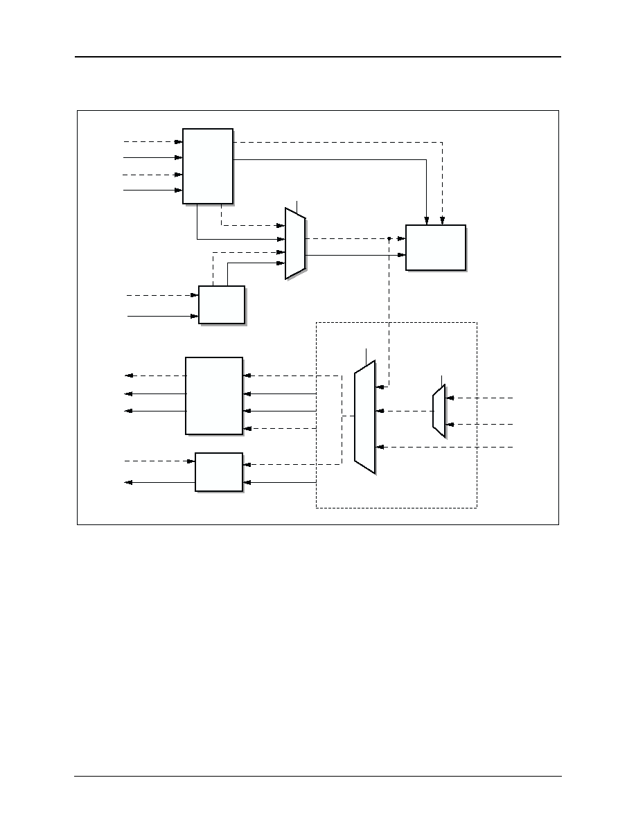
4-2
Mindspeed TechnologiesTM
500238B
Advance Information
Clock Sources and Clock Configurations
CX29503 Data Sheet
Figure 4-1. DS3/E3 Framer Clock and Data Paths on Line Side
0
1
CLK_TXDS3
CLK_TXE3
TXE3_CLKSEL
(default: 0)
RLINECLK
2, 3
0, 1
SI-Bus Rx
Interface
SIB_RXHSCLK
CK_SRC[0:1]
RXCLKI
1
2, 3
0
upl3trclkset[0:1]
(default: 0)
DS3/E3
Rx Framer
(line side)
clt_clk_l3txcki
SIB_RXDAT
RXPOS
RXCLKI
LINECK
RXPOS/RXNRZ
RXNEG
SI-Bus Tx
Interface
SIB_TXHSCLK
SIB_TXDAT
TXPOS
DS3/E3
Tx Serial
Interface
TLINECLK
DS3/E3 Tx Framer (line side)
TXNEG
RLINECLK
RXPOS
DS3/E3
Rx Serial
Interface
RXNEG
RXCLKI
m13_clk_txlinext
m13_txneg
m13_txpos
VCO
m13_vco
m13_clk_txlineo
m13_txnrz
100702_032

500238B
Mindspeed TechnologiesTM
4
-
3
Advance Information
CX29503 Data Sheet
Clock Sources and Clock Configurations
4.2
DS1/E1 Clock and Data Options
The line side of each DS1/E1 framer interfaces to the M13 MUX/DEMUX and to the
SONET tributary mapper. The system side of each DS1/E1 framer interfaces to the
TSB. The MUXes that control clock and data paths to 28 of the DS1/E1 transmit and
receive framers are shown in
Figure 4-2
. See
Figure 2-2
for the top level view of the
interfaces shown in
Figure 4-2
.
If the default value of a MUX is not desired, a clock must still be provided to the
default input to allow the MUX to be changed by a register that is in a downstream
block. In addition, the desired clock must be active before the MUX is switched to that
clock.
Figure 4-2. DS1/E1 Framer Clock and Data Paths
smx_dat_rx
m13_rxdat_fr1
XMTR_SEL_n
m13_rxclk_fr1
smx_clk_rx
RCVR_SEL
FLOOP
RCKI
fr1_rxclk_tsb
fr1_txclk_tsb
fr1_clk_tx
fr1_txclk_m13
CLK_TXDS1 CLK_TXE1
2, 3
0
1
M13/E13
MUX
DEMUX
1
0
28xDS1/E1
Receivers
TSB
Rx
28xDS1/E1
Transmitters
DS1/VT1.5, E1/VT2.0,
DS1/VC-11, and E1/VC-12
Tributary Mapper
0
1
RPOSI
RPCMO
TSB
Tx
TSBCKI
TPCMI
M13/E13
MUX
DEMUX
DS1/VT1.5, E1/VT2.0,
DS1/VC-11, and E1/VC-12
Tributary Mapper
TPOSO
fr1_txdat_m13
TDLCKO
RDLCKO,
RFSYNC
TFSYNC
fr1_dat_tx
100702_033

4-4
Mindspeed TechnologiesTM
500238B
Advance Information
Clock Sources and Clock Configurations
CX29503 Data Sheet
4.3
SI-Bus Interface Mode
In the SI-Bus Interface mode, the line side of the device is connected to an external
SONET/SDH MUX device via the SI-Bus.
Table 4-1
shows the clocking sources
required in this mode. This mode is enabled by setting the CK_SRC[1:0] pins to 0
◊
0
or 0
◊
1.
4.3.1
DS3/E3 Clock and Data Configurations (SI-Bus Interface Mode)
The MUXes shown in
Figure 4-1
are configured based on the Timing (system or loop
timing) and DS3/E3 modes (DS3 or E3).
Tables 4-2
and
4-3
show the configuration
settings for the DS3 and E3 modes, respectively.
Tables 4-2
and
4-3
assume the
CK_SRC[1:0] pins are set to 0
◊
0 or 0
◊
1.
If the data path is unchannelized STS-1, then the line clocks (m13_clk_txtlineo and
LINECLK) listed in
Tables 4-2
and
4-3
are not needed. Furthermore, the complete
DS3/E3 framer can be disabled by clearing the FrEnable bit in the DS3/E3 Framer
Control register (See
Section 8.4.1
).
Table 4-1. SI-Bus Clock Sources in SI-Bus Interface Mode
Pin Description
Freq. (MHz)
Timing Mode
Clock Source
SIB_RXHSCLK
51.84
System or Looped
External SONET/SDH MUX
(CX29610)
SIB_TXHSCLK
51.84
System or Looped
External SONET/SDH MUX
(CX29610)
SIB_RXCLK
19.44
System or Looped
External SONET/SDH MUX
(CX29610)
SIB_TXCLK
19.44
System or Looped
External SONET/SDH MUX
(CX29610)
Table 4-2. DS3 Clock Sources and Configuration Bits in SI-Bus Interface Mode
Description
Freq.
(MHz)
Timing Mode
Clock
Source
Configuration Bits
(1)
DS3 Receive Framer Line
Clock (LINECLK)
44.736
System or Looped
SONET Block
--
DS3 Transmit Framer Line
Clock (m13_clk_txlineo)
44.736
System
CLK_TXDS3
upl3txclkset[1:0] = 0
◊
1
TXE3_CLKSEL = 0
◊
0
Looped
LINECLK
upl3txclkset[1:0] = 0
◊
0
TXE3_CLKSEL = Don't Care
FOOTNOTE:
(1)
upl3txclkset[1:0] is located in the M13/E13 System Control register (
Section 8.4.1
).
TXE3_CLKSEL is located in the Clock Configuration register (
Section 8.8
).

500238B
Mindspeed TechnologiesTM
4
-
5
Advance Information
CX29503 Data Sheet
Clock Sources and Clock Configurations
4.3.2
DS1/E1 Clock and Data Configurations (SI-Bus Interface Mode)
The MUXes shown in
Figure 4-2
are configured based on the Timing (system or loop
timing) and DS1/E1 modes (DS1 or E1).
Tables 4-4
and
4-5
list the configuration
settings for the DS1 and E1 modes, respectively.
Tables 4-4
and
4-4
assume the
CK_SRC[1:0] pins are set to 0
◊
0 or 0
◊
1.
If the data path is unchannelized STS-1 or unchannelized DS3/E3, then the line and
system clocks listed in
Tables 4-4
and
4-4
are not needed. Furthermore, the DS1/E1
framers can be disabled by setting RABORT in the Receiver Configuration register
(
Section 8.3.2.5
).
Table 4-3. E3 Clock Sources and Configuration Bits in SI-Bus Interface Mode
Description
Freq.
(MHz)
Timing Mode
Clock
Source
Configuration Bits
(1)
E3 Receive Framer Line Clock
(LINECLK)
34.368
System or Looped
SONET Block
--
E3 Transmit Framer Line
Clock (m13_clk_txlineo)
34.368
System
CLK_TXE3
upl3txclkset[1:0] = 0
◊
1
TXE3_CLKSEL = 0
◊
1
Looped
LINECLK
upl3txclkset[1:0] = 0
◊
0
TXE3_CLKSEL = Don't Care
FOOTNOTE:
(1)
upl3txclkset[1:0] is located in the M13/E13 System Control register (
Section 8.4.1
).
TXE3_CLKSEL is located in the Clock Configuration register (
Section 8.8
).
Table 4-4. DS1 Clock Sources and Configuration Bits in SI-Bus Interface Mode
Description
Freq.
(MHz)
Timing Mode
Clock Source
Configuration Bits
(1)
DS1 Receive Framer Line
Clock (RCKI)
1.544
System or Looped
M13/E13 Block
RCVR_SEL = 0
◊
0
FLOOP = 0
◊
0
SONET Tributary
Mapper
RCVR_SEL = 0
◊
1
FLOOP = 0
◊
0
DS1 Transmit Framer System
Clock (TSBCKI) and Line
Clocks (fr1_txclk_m13 and
fr1_clk_tx)
1.544 System
CLK_TXDS1
XMTR_SEL_n[1:0]
=
0
◊
00
Looped
Receive DS1 Clock
XMTR_SEL_n[1:0] = 0
◊
2 or
0
◊
3
FOOTNOTE:
(1)
XMTR_SEL_n[1:0] is located in Framer Control Registers 1 and 2 (
Section 8.3.1
).
RCVR_SEL is located in Framer Control Register 1 (
Section 8.3.1
).
FLOOP is located in the Rollback Configuration Register (
Section 8.3.2.4
).

4-6
Mindspeed TechnologiesTM
500238B
Advance Information
Clock Sources and Clock Configurations
CX29503 Data Sheet
Table 4-5. E1 Clock Sources and Configuration Bits in SI-Bus Interface Mode
Description
Freq.
(MHz)
Timing Mode
Clock Source
Configuration Bits
(1)
E1 Receive Framer Line Clock
(RCKI)
2.048
System or Looped
M13/E13 Block
RCVR_SEL = 0
◊
0
FLOOP = 0
◊
0
SONET Block
RCVR_SEL = 0
◊
1
FLOOP = 0
◊
0
E1 Transmit Framer System
(TSBCKI) and Line Clocks
(fr1_txclk_m13 and
fr1_clk_tx)
2.048
System CLK_TXE1
XMTR_SEL_n[1:0]
=
0
◊
01
Looped
Receive E1 Clock
XMTR_SEL_n[1:0] = 0
◊
2
or 0
◊
3
FOOTNOTE:
(1)
XMTR_SEL_n[1:0] is located in Framer Control register 1 and 2 (
Section 8.3.1
).
RCVR_SEL is located in Framer Control register 1 (
Section 8.3.1
).
FLOOP is located in the Loopback Configuration register (
Section 8.3.2.4
).

500238B
Mindspeed TechnologiesTM
4
-
7
Advance Information
CX29503 Data Sheet
Clock Sources and Clock Configurations
4.4
Serial DS3 Interface Mode
In the serial DS3 interface mode, typically, the line side of the device is connected to
an external LIU.
Table 4-6
lists the external clocking required in this mode. This mode
is enabled by setting the CK_SRC[1:0] pins to 0
◊
2 or 0
◊
3.
Table 4-7
lists the configuration settings depending on the timing mode. If the data
path is unchannelized DS3, then all DS1 framers can be disabled by setting RABORT
in the Receiver Configuration register (
Section 8.3.2.5
).
Table 4-6. DS3 Clock Sources and Configuration Bits in Serial DS3 Interface Mode
Description
Freq.
(MHz)
Timing Mode
Clock Source
Configuration Bits
(1)
DS3 Receive Framer Line
Clock
(LINECLK)
44.736
System or Looped
RLINECLK
--
DS3 Transmit Framer Line
Clock (m13_clk_txlineo)
44.736
System
CLK_TXDS3
upl3txclkset[1:0] = 0
◊
1
TXE3_CLKSEL = 0
◊
0
Looped
LINECLK
upl3txclkset[1:0] = 0
◊
0
TXE3_CLKSEL = Don't Care
RXCKI
upl3txclkset[1:0] = 0
◊
2 or
0
◊
3
TXE3_CLKSEL = Don't Care
FOOTNOTE:
(1)
upl3txclkset[1:0] is located in the M13/E13 System Control register (
Section 8.4.1
).
TXE3_CLKSEL is located in the Clock Configuration register (
Section 8.8
).
Table 4-7. DS1 Clock Sources and Configuration Bits in Serial DS3 Interface Mode
Description
Freq.
(MHz)
Timing Mode
Clock Source
Configuration Bits
(1)
DS1 Receive Framer Line
Clock (RCKI)
1.544
System or Looped
M13/E13 Block
RCVR_SEL = 0
◊
0
FLOOP = 0
◊
0
DS1 Transmit Framer System
Clock (TSBCKI) and Line
Clocks (fr1_txclk_m13 and
fr1_clk_tx)
1.544
System CLK_TXDS1
XMTR_SEL_n[1:0]
=
0
◊
00
Looped
Receive DS1 Clock
XMTR_SEL_n[1:0] = 0
◊
1X
FOOTNOTE:
(1)
XMTR_SEL_n[1:0] is located in Framer Control Registers 1 and 2 (
Section 8.3.1
).
RCVR_SEL is located in Framer Control Register 1 (
Section 8.3.1
).
FLOOP is located in the Loopback Configuration register (
Section 8.3.2.4
).

4-8
Mindspeed TechnologiesTM
500238B
Advance Information
Clock Sources and Clock Configurations
CX29503 Data Sheet
4.5
Serial E3 Interface Mode
In the serial E3 Interface mode, typically the line side of the device is connected to an
external LIU.
Table 4-8
lists the external clocking required in this mode. This mode is
enabled by setting the CK_SRC[1:0] pins to 0
◊
2 or 0
◊
3 and setting the
TXE3_CLKSEL in the Clock Configuration register in the Clock and Test (CLT)
block to 1.
Table 4-9
lists the configuration settings depending on the timing mode. If the data
path is an unchannelized E3, then all E1 framers can be disabled by setting RABORT
in the Receiver Configuration register (
Section 8.3.2.5
).
Table 4-8. E3 Clock Sources and Configuration Bits in Serial E3 Interface Mode
Description
Freq.
(MHz)
Timing Mode
Clock Source
Configuration Bits
(1)
Receive E3 and M13
Reference Clocks
34.368
System or Looped
RLINECLK
from LIU
--
Transmit E3 and E13
Reference Clocks
34.368
System
CLK_TXE3
upl3txclkset[1:0] = 0
◊
1
TXE3_CLKSEL = 0
◊
1
Looped RLINECLK
from LIU
upl3txclkset[1:0] = 0
◊
0
TXE3_CLKSEL = Don't Care
RXCKI
upl3txclkset[1:0] = 0
◊
2 or
0
◊
3
TXE3_CLKSEL = Don't Care
FOOTNOTE:
(1)
upl3txclkset[1:0] is located in the M13/E13 System Control registers (
Section 8.4.1
).
TXE3_CLKSEL is located in the Clock Configuration register (
Section 8.8
).
L3Map[1:0] is located in SONET Level 3 Mapping Control (
Section 8.5.7
).
Table 4-9. E1 Clock Sources and Configuration Bits in Serial E3 Interface Mode
Description
Freq.
(MHz)
Timing Mode
Clock Source
Configuration Bits
(1)
E1 Receive Framer Line Clock
(RCKI)
2.048
System or Looped
M13/E13 Block
RCVR_SEL = 0
◊
0
FLOOP = 0
◊
0
E1 Transmit Framer System
Clock (TSBCKI) and Line
Clocks (fr1_txclk_m13 and
fr1_clk_tx)
2.048 System
CLK_TXE1
XMTR_SEL_n[1:0]
=
0
◊
00
Looped
Receive E1 Clock
XMTR_SEL_n[1:0] = 0
◊
1X
FOOTNOTE:
(1)
XMTR_SEL_n[1:0] is located in Framer Control Registers 1 and 2 (
Section 8.3.1
).
RCVR_SEL is located in Framer Control Register 1 (
Section 8.3.1
).
FLOOP is located in the Loopback Configuration register (
Section 8.3.2.4
).
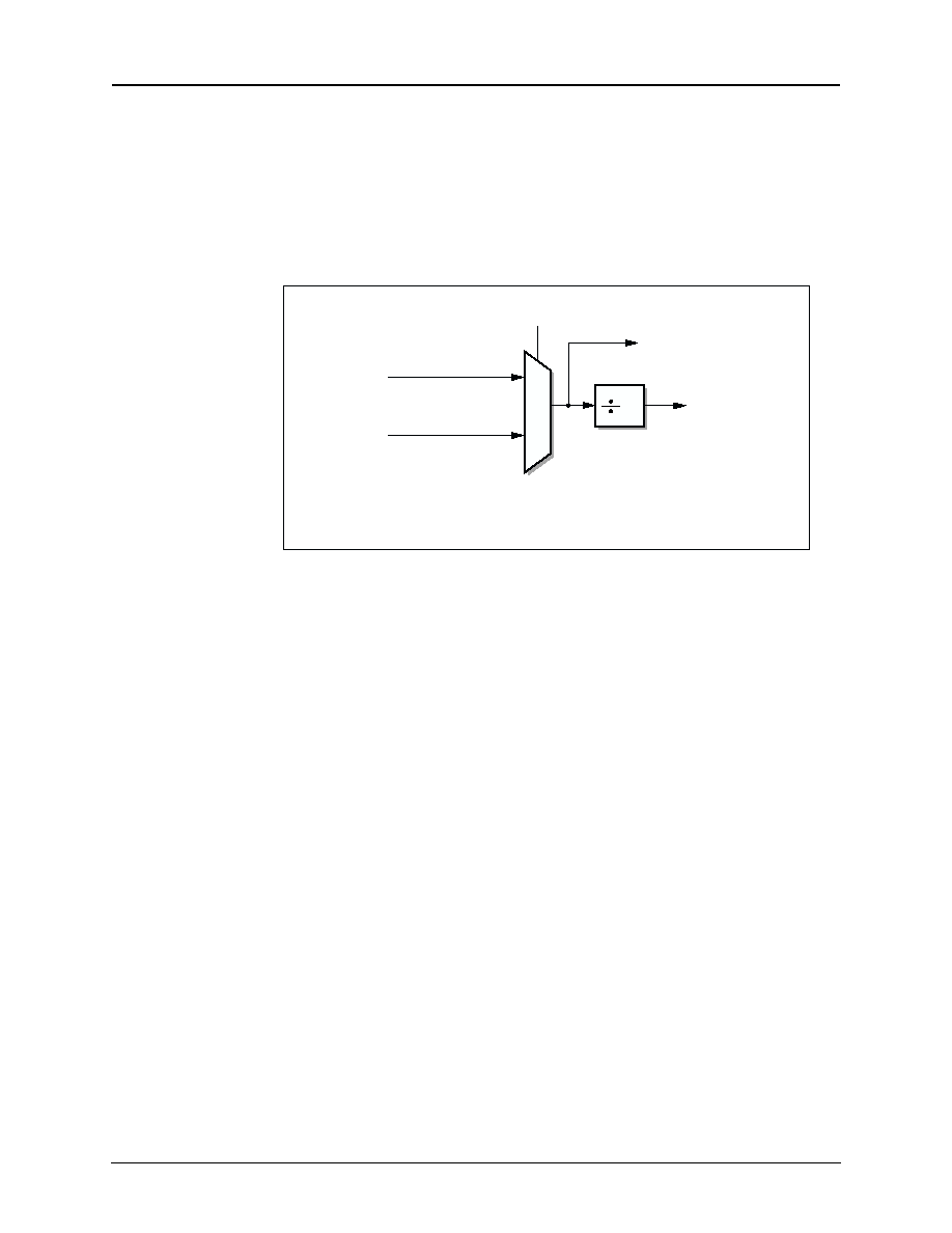
500238B
Mindspeed TechnologiesTM
4
-
9
Advance Information
CX29503 Data Sheet
Clock Sources and Clock Configurations
4.6
Payload TSB and Overhead TSB Clocks
The Payload TSB (TSB_CLK) and Overhead TSB clocks (TSB_OCLK) are derived
as shown in
Figure 4-3
. The clock frequencies depend on the configurations as listed
in
Table 4-10
for TSB_CLK and
Table 4-11
for TSB_OCLK.
Figure 4-3. TSB Payload Clock and TSB Overhead Clock Sources
CLK_TXDS3
CLK_SRC[0:1]
2, 3
0, 1
TXHSCLK
4
TSB_CLK
TSB_OCLK
100702_034

4-10
Mindspeed TechnologiesTM
500238B
Advance Information
Clock Sources and Clock Configurations
CX29503 Data Sheet
4.7
Command and Status Processor (CSP) and
Microprocessor Clocks
The clocks for the CSP and Microprocessor Interface blocks are derived as shown in
Figure 4-4
. The CSP block utilizes line transmit clock sources for its internal
operation. From the external point of view, the CSP operates in an asynchronous mode.
Table 4-10. Payload TSB Clock Configurations
Description
Freq.MHz
Line
Interface
Table 2-7
Row Number
(TSB Signal Type)
Clock Source
Configuration Bits
(1)
Payload Clock
(TSB_CLK) in TSB
Mode (TSBUS =
0
◊
1
(1)
)
51.84
SI-Bus
7
(
Table 2-7
(1)
)
SIB_TXHSCLK
CK_SRC[1:0] pins = 0
◊
0 or 0
◊
1
44.736
Serial DS3
2, 3, and 4
(28
◊
DS1, 21
◊
E1,
or mixed DS1/E1)
CLK_TXDS3
CK_SRC[1:0] pins = 0
◊
2
or 0
◊
3
CLEAR_DS3 = 0
◊
0
34.368 Serial
E3
6
(16
◊
E1)
CLK_TXDS3
CK_SRC[1:0] pins = 0
◊
2
or 0
◊
3
CLEAR__E3 = 0
◊
0
44.736 Serial
DS3
1
(unchannelized DS3)
CLK_TXDS3
CK_SRC[1:0] pins = 0
◊
2
or 0
◊
3
CLEAR_DS3 = 0
◊
1
34.368 Serial
E3
5
(unchannelized E3)
CLK_TXDS3
CK_SRC[1:0] pins = 0
◊
2
or 0
◊
3
CLEAR_E3 = 0
◊
1
FOOTNOTE:
(1)
TXE3_CLKSEL is located in the Clock Configuration register (
Section 8.8
).
TSBUS, CLEAR_DS3, and CLEAR_E3 are located in the TSB Module Operation (
Section 8.8
).
Table 4-11. Overhead TSB Clock Configurations
Description
Freq. MHz
TSB Data Path
Clock Source
Configuration Bits
(1)
Overhead TSB Clock
(TSB_OCLK)
12.96
--
SIB_TXHSCLK / 4
CK_SRC[1:0] pins = 0
◊
0
or 0
◊
1
11.184
--
CLK_TXDS3 / 4
CK_SRC[1:0] pins = 0
◊
2
or 0
◊
3
TXE3_CLKSEL = 0
◊
0
8.592
--
CLK_TXE3 / 4
CK_SRC[1:0] pins = 0
◊
2
or 0
◊
3
TXE3_CLKSEL = 0
◊
1
FOOTNOTE:
(1)
TXE3_CLKSEL is located in the Clock Configuration register (
Section 8.8
).
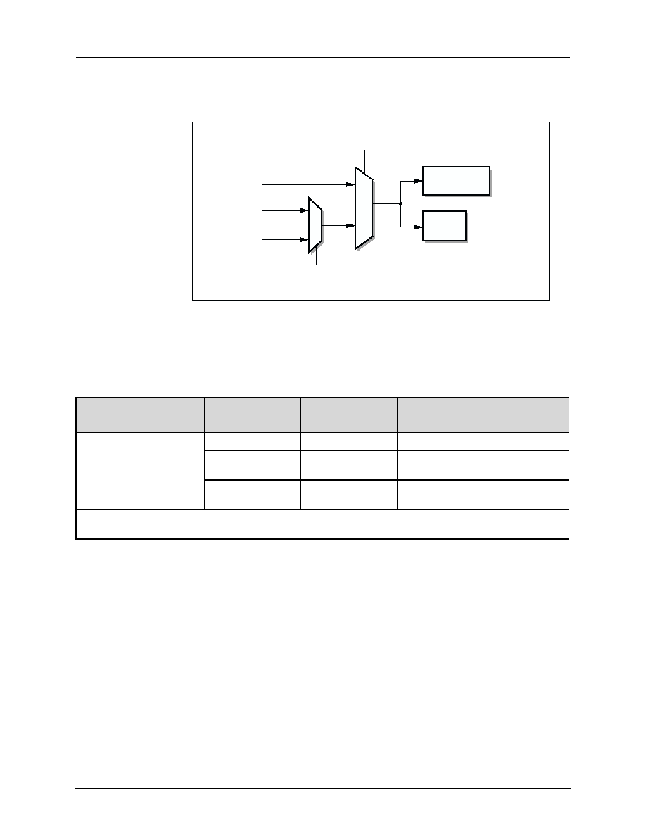
500238B
Mindspeed TechnologiesTM
4
-
11
Advance Information
CX29503 Data Sheet
Clock Sources and Clock Configurations
Depending on the line side interfaces, the CSP operates internally at different
frequencies as shown in
Table 4-12
. The CSP clock is an internal clock only, and it is
not provided on any external pins.
Figure 4-4. CSP and Microprocessor Clock Sources
CLK_TXDS3
CLK_TXE3
0
1
TXE3_CLKSEL
(default = 0)
Microprocessor
Block
CSP
Block
CK_SRC[0:1]
2, 3
0, 1
TXHSCLK
100702_035
Table 4-12. CSP and Microprocessor Clock Configurations
Description
Freq.
(MHz)
Clock Source
Configuration Bits
(1)
CSP and Microprocessor
Clocks
51.84
SIB_TXHSCLK
CK_SRC[1:0] pins = 0
◊
0 or 0
◊
1
44.736
CLK_TXDS3
CK_SRC[1:0] pins = 0
◊
2 or 0
◊
3
TXE3_CLKSEL = 0
◊
0
34.368
CLK_TXE3
CK_SRC[1:0] pins = 0
◊
2 or 0
◊
3
TXE3_CLKSEL = 0
◊
1
FOOTNOTE:
(1)
TXE3_CLKSEL is located in the Clock Configuration register (
Section 8.8
).

4-12
Mindspeed TechnologiesTM
500238B
Advance Information
Clock Sources and Clock Configurations
CX29503 Data Sheet
4.8
DS1/E1 System and Microprocessor Clocks
The clocks for the DS1/E1 system and microprocessor clocks are derived as shown in
Figure 4-5
. The clock frequencies depend on the configurations as listed in
Table 4-13
.
Figure 4-5. DS1/E1 System Clock and Microprocessor Clock Sources
CLK_TXDS3
CLK_TXE3
0
1
TXE3_CLKSEL
(default = 0)
Divide
Down
SYSCI
MCLK
DS1/E1
Framers
CK_SRC[0:1]
2, 3
0, 1
TXHSCLK
100702_036
Table 4-13. DS1/E1 System and DS1/E1 Microprocessor Clock Configurations
Description
Freq.
(MHz)
Clock Source
Configuration Bits
(1)
DS1/E1 System Clock
(SYSCKI)
25.92
SIB_TXHSCLK / 2
CK_SRC[1:0] pins = 0
◊
0 or 0
◊
1
22.368
CLK_TXDS3 / 2
CK_SRC[1:0] pins = 0
◊
2 or 0
◊
3
TXE3_CLKSEL = 0
◊
0
17.184
CLK_TXE3 / 2
CK_SRC[1:0] pins = 0
◊
2 or 0
◊
3
TXE3_CLKSEL = 0
◊
1
DS1/E1 Microprocessor
Clock (MCLK)
25.92
SIB_TXHSCLK / 2
CK_SRC[1:0] pins = 0
◊
0 or 0
◊
1
22.368
CLK_TXDS3 / 2
CK_SRC[1:0] pins = 0
◊
2 or 0
◊
3
TXE3_CLKSEL = 0
◊
0
34.368
CLK_TXE3
CK_SRC[1:0] pins = 0
◊
2 or 0
◊
3
TXE3_CLKSEL = 0
◊
1
FOOTNOTE:
(1)
TXE3_CLKSEL is located in Clock Configuration register (
Section 8.8
).

500238B
Mindspeed TechnologiesTM
4
-
13
Advance Information
CX29503 Data Sheet
Clock Sources and Clock Configurations
4.9
One Hertz Clock
The 1 Hz clock latches performance counters throughout the CX29503. The source of
this clock depends on the configuration of the CK_SRC[1:0] pins, the
ONE_HZ_OEN and TXE3_CLKSEL configuration bits as listed in
Table 4-14
. The
ONE_HZ_OEN bit controls whether the CLK_1HZ pin is an input or an output.
Table 4-14. Selections for the One Hertz Clock Source and CLK_1HZ Pin
Selections
Outcomes
ONE_HZ_OEN
(1)
CK_SRC[1:0] Pins
TXE3_CLKSEL
(1)
One Hz Clock
Source
CLK_1HZ Pin
1
Don't Care
Don't Care
Sourced from
CLK_1HZ pin
1 Hz input
0
0
◊
0 or 0
◊
1
Don't Care
Divided down from
SIB_TXHSCLK
Output divided down from
SIB_TXHSCLK
0
0
◊
2 or 0
◊
3
0
Divided down from
CLK_TXDS3
Output divided down from
CLK_TXDS3
0
0
◊
2 or 0
◊
3
1
Divided down from
CLK_TXE3
Output divided down from
CLK_TXE3
(1)
(1)
ONE_HZ_OEN and TXE3_CLKSEL are located in the Clock Configuration register (
Section 8.8
).

4-14
Mindspeed TechnologiesTM
500238B
Advance Information
Clock Sources and Clock Configurations
CX29503 Data Sheet

500238B
Mindspeed TechnologiesTM
5
-
1
Advance Information
5.0 Loopbacks
The CX29503 supports a full set of line and system side loopbacks.
5.1
DS3/E3 Framer and M13 MUX Loopbacks
The loopbacks available in the DS3/DS2/DS1 block are shown in
Table 5-1
. All
loopbacks operate on a per tributary basis. All line loopback features defined for DS3/
DS2/DS1 will also apply for E3/E2/E1 signals.
!
Type 1 Loopback (DS3 Payload Loopback)--Supports the DS3 FEAC-based DS3
loopback. FEAC patterns are reported in status registers. The software is capable
of activating/deactivating the DS3 loopback based on this status bit and optionally
inserting Alarm Indication Signals (AIS) to downstream components. The
software is capable of inserting this code into transmitted DS3 overhead bits.
!
Type 2 Loopback (DS3-Activated DS2 Line Loopback)--DS3-C bit stream is
examined for a DS2 loopback sequence. The software is capable of enabling/
disabling this feature and optionally inserting AISs to downstream components. If
this feature is enabled by the software, the hardware shall autonomously enable
loopback when a loopback command is received.
If the software has requested AIS insertion, the hardware inserts the AIS to the
downstream components for the duration of the loopback. The hardware will
indicate via a status bit that a loopback is in process. The hardware will
autonomously terminate the loopback after receiving the appropriate command in
the C-bit stream and update the status register. The software is capable of inserting
this DS2 loopback code into transmitted DS3 overhead bits.
This loopback requires M13 multiplexing and, therefore, is not applicable in C-bit
parity mode.
Figure 5-1. DS3/E3 Loopback Definitions
100702_037
B3ZS/
HDB3
M23/E23
DS3/E3
DS2/E2
M12/E12
Rx
Tx
Framer
Type 5
Type 2
Type 4
Type 1
Type 8
Type 6
Framer
MUX
MUX

5-2
Mindspeed TechnologiesTM
500238B
Advance Information
Loopbacks
CX29503 Data Sheet
!
Type 4 Loopback (DS2-Activated DS1 Line Loopback)--The DS2-C bit stream is
examined for a DS1 loopback sequence. The software is capable of enabling/
disabling this feature and optionally inserting AISs to downstream components. If
this feature is enabled by the software, the hardware will autonomously enable
loopback when a loopback command is received.
If the software has requested AIS insertion, the hardware will insert an AIS to
downstream components for the duration of the loopback. The hardware will
indicate, via a status bit, that a loopback is in process. The hardware will
autonomously terminate the loopback after receiving the appropriate command in
the C-bit stream and update the status register. The software is capable of inserting
this DS1 loopback code into transmitted DS2 overhead bits.
!
Type 5 Loopback (DS3 Source Loopback)--DS3 TX-to-RX loopback is
implemented. This loopback feature is activated/deactivated under software
control. The transmitted signal stream is fed into the receive path. DS3 input
signals at the RPOS and RNEG pins are ignored. The Receive clock is substituted
by the Transmit clock. The software may choose to issue an AIS or LOS indication
on the DS3 transmit pins, TPOS and TNEG.
!
Type 6 Loopback (DS3 Shallow Line Loopback)--The DS3 RX-to-TX loopback is
implemented. This loopback feature is activated/deactivated under software
control. The received signal is echoed on the transmit pins TPOS and TNEG. The
Transmit clock is substituted with the Receive clock. Signals on RNEG and RPOS
are fed to the DS3 framer. The software will have the option of inserting an AIS at
the DS3 framer output instead of demultiplexed signals.
!
Type 8 Loopback (DS3 Remote Line Loopback)--The DS3 remote line loopback
is implemented. This loopback feature is activated/deactivated under software
control. The received signal after B3ZS/HDB3 decoding is looped back to the
transmitter B3ZS/HDB3 encoder.

500238B
Mindspeed TechnologiesTM
5
-
3
Advance Information
CX29503 Data Sheet
Loopbacks
5.2
DS1/E1 Framer Loopbacks
The loopbacks available in the DS1/E1 Framer block are shown in
Figure 5-2
. The
drawing shows clock MUXes but not data MUXes to minimize clutter. The clock
source for each mode is listed in
Table 5-1
.
!
Framer Loopback--All transmitted data is looped back to the receiver. This
loopback is activated by setting the Local Framer Loopback (FLOOP) bit in the
Loopback Configuration register [DS1/E1 Framer block, addr: 014].
!
Line Loopback--The line loopback loops the Receiver inputs to the Transmitter
outputs. The loopback provides BPV transparency and the ability to override the
looped data with AIS. The Receiver data path is not affected by the activation of
this loopback. The remote Line Loopback (LLOOP) is activated by setting the
Remote Line Loopback bit in the Loopback Configuration register [DS1/E1
Framer Block, addr: 014]. It is possible to operate the remote line loopback
simultaneously with Local Framer loopback.
!
Payload Loopback--This loopback only loops the received payload data back to the
transmitter. The overhead data is a continuous source from the transmitter. Because
the transmitting data is driven by the transmit clock, the received payload data
passes through a 64-bit a FIFO to accommodate receiver jitter (mainly introduced
by the VT mapper). This loopback is activated by setting the Unchannelized
Payload Loopback (UPLOOP) bit in the Loopback Configuration register [DS1/E1
Framer Block, addr: 014].
Figure 5-2. DS1/E1 Framer Loopbacks
100702_038
Receiver
Transmitter
M13 Rx Data
SONET Rx Data
M13 Rx clock
SONET Rx clock
M13 Tx Data
SONET Tx Data
DS1 Reference Clock
E1 Reference Clock
TSB Tx Data
TSB Rx Data
DS1/E1 Framer
Framer
Loopback
Line
Loopback
Payload
Loopback
64-bit
FIFO
Table 5-1. Clock Sources for DS1/E1 Loopback Modes
Loopback
Receiver Clock Source
Transmitter Clock Source
Framer
DS1 or E1 reference clock
DS1 or E1 reference clock
Line
M13 or SONET Rx clock
M13 or SONET Rx clock
Payload
M13 or SONET Rx clock
DS1 or E1 reference clock

5-4
Mindspeed TechnologiesTM
500238B
Advance Information
Loopbacks
CX29503 Data Sheet
5.3
SI-Bus System Side Loopback
The transmitter is looped back to the receiver via the Loopback control and is
provided for diagnostic purposes, as shown in
Figure 5-3
. When enabled, this block
controls the RxStart and TxStart signals so that the Receiver is synchronized with the
Transmitter. The Transmitter SI-Bus data and parity can then be directly looped to the
Receiver SI-Bus data and parity. The clocks required for this function are the 51.84
and 19.44 MHz SI-Bus Transmit clocks. This loopback is activated by setting the
TxRxLoopBk bit in the SI-Bus Transmit to Receive Loopback Control register
[SONET/SDH General Control/Status Block, addr: 0x6007,
page 8-170
].
Figure 5-3. SI-Bus System Side Loopback
CX29503, One Slice
100702_055
SI-BUS
TX DATA

500238B
Mindspeed TechnologiesTM
6
-
1
Advance Information
6.0 Path Conditioning
This section discusses the path conditioning (also called alarm generation) required
on the receive (downstream) and transmit (upstream) data paths. Path conditioning is
dictated by international standards. The detection is based on the monitoring of the
receive data. The path conditioning consists of both software processing by the CSP
and automatic processing within the logic of the CX29503 and CX29610.
In the CX29503, all defects are detected by the hardware and all failures are
integrated by the CSP.
6.1
STS-1 Path Conditioning
Table 6-1
lists the STS-1 Path Conditioning. The upstream path conditioning is
performed by the CX29610. The CX29610 can be programmed to automatically
perform the upstream path conditioning. On the CX29503, an auto-insertion function
is provided for downstream path conditioning.
Table 6-1. STS-1 Path Conditioning
Defect
CX29610 Processing
CX29503 Processing
Action to Upstream
Action to Downstream (DS3)
Action to Downstream
(VT with DS1/E1)
Path
Conditioning
Latency
Path
Conditioning
Latency
Path
Conditioning
Latency
AIS-P
RDI-P
N/A
AIS
375 µs
AIS-V
500 µs
AIS-L
RDI-P and RDI-L
N/A
AIS
375 µs
AIS-V
500 µs
LOP-P
RDI-P
N/A
AIS
375 µs
ASI-V
500 µs
LOF
RDI-P and RDI-L
N/A
AIS
375 µs
AIS-V
500 µs
UNEQ-P
RDI-P
N/A
N/A
(1)
N/A
N/A
(1)
N/A
PLM-P
RDI-P
N/A
N/A
(1)
N/A
N/A
(1)
N/A
TIM-P
Reported in register
N/A
N/A
(2)
N/A
N/A
(2)
N/A
LOS
RDI-P and RDI-L
N/A
N/A
125 µs
AIS-V
500 µs
LOM
None
N/A
Reported in
register
(3)
N/A
Reported in
register
(3)
N/A
FOOTNOTE:
(1)
If an UNEQ-P or PLM-P defect occurs, the CX29610 automatically generates AIS-P, and the CX29503 detects the AIS-P and
performs the processing indicated for AIS-P.
(2)
If a TIM-P defect occurs, the CX29610 reports the defect in a register and the CX29610 driver software enables AIS-P.
(3)
If an LOM defect (i.e., 5 consecutive H4 values are not in the correct sequence) occurs, the CX29503 reports the defect in a
register.

6-2
Mindspeed TechnologiesTM
500238B
Advance Information
Path Conditioning
CX29503 Data Sheet
6.2
DS3 Path Conditioning
DS3 path conditioning is shown in
Table 6-2
. The RAI insertion is performed by the
CSP through integration of event conditions. A software configurable auto-insertion
function is provided for downstream path conditioning.
Instead of the typical DS3 AIS pattern of an alternating pattern of 1s and 0s, the
CX29503 implements the DS3 AIS pattern as unchannelized all 1s to force the
CX28500 device to abort the message transaction.
6.3
E3 Path Conditioning
E3 path conditioning is shown in
Table 6-3
. A software configurable auto-insertion
function is provided for downstream path conditioning.
Table 6-2. DS3 Path Conditioning
Defect
Action to
Upstream
Latency
Action to Downstream
Latency
AIS
RAI
AIS-fail:
AIS alarm condition persists for 2.0 s
Unchannelized all 1s
Immediately
LOS
RAI
LOS-fail:
LOS alarm condition persists for 2.0 s
Unchannelized all 1s
Immediately
LOF
RAI
LOF-fail:
OOF condition persists for 2.0 s
Unchannelized all 1s
Immediately
IDLE
N/A
N/A
Unchannelized all 1s
Immediately
Table 6-3. E3 Path Conditioning
Defect
Action toUpstream
Latency
Action to
Downstream
Latency
LOS
RAI
1 ms
AIS
1 ms
OOF
RAI
1 ms
AIS
1 ms
GENERAL NOTE:
1. E3 AIS is an unchannelized all 1s signal.

500238B
Mindspeed TechnologiesTM
6
-
3
Advance Information
CX29503 Data Sheet
Path Conditioning
6.4
DS2 Path Conditioning
DS2 path conditioning is shown in
Table 6-4
. Because the path condition latency at
this level is not defined in the ANSI T1.213 specification, a software configurable
auto-insertion function is provided for upstream path conditioning.
6.5
E2 Path Conditioning
DS2 path conditioning is shown in
Table 6-5
. At the E2 level, a software configurable
auto-insertion function is provided for both directions.
Table 6-4. DS2 Path Conditioning
Defect
Action to Upstream
Latency
Action to
Downstream
Latency
AIS
RAI
Not defined
AIS
Immediately
OOF
RAI
Not defined
AIS
Immediately
LOS
RAI
Not defined
AIS
Immediately
Table 6-5. E2 Path Conditioning
Defect
Action toUpstream
Latency
Action to
Downstream
Latency
LOS
RAI
1 ms
AIS
1 ms
OOF
RAI
1 ms
AIS
1 ms

6-4
Mindspeed TechnologiesTM
500238B
Advance Information
Path Conditioning
CX29503 Data Sheet
6.6
VT Path Conditioning
Path conditioning for the VT group is shown in
Table 6-6
. As specified in GR253, the
RDI and ERDI should respond to the incoming defect within 100 ms for at least 10
superframes (5 ms). The auto-insertion capability is designed to provide at least a 5
ms trigger delay. A software configurable auto-insertion function is provided for
downstream path conditioning.
6.7
DS1/E1 Path Conditioning
DS2 path conditioning is shown in
Table 6-7
. Path conditioning at DS1 level operates
in a software configurable auto-insertion fashion.
Table 6-6. VT Path Conditioning
Defect
Action to Upstream
Action to Downstream
Path Condition
Latency
DS1/E1 Framer
Path Cond.
Latency
LOP-V
RDI-V
ERDI-V (101)
< 100 ms
AIS
125 µs
AIS-V
RDI-V
ERDI-V (101)
< 100 ms
AIS
125 µs
UNEQ-V
RDI-V
ERDI-V (110)
< 100 ms
AIS
125 µs
PLM-V
RDI-V
ERDI-V (010)
< 100 ms
AIS
125 µs
Unsupported VT
N/A
N/A
AIS
125 µs
Table 6-7. DS1/E1 Path Conditioning
Defect
Action to
Upstream
Latency
Action to
Downstream
Latency
AIS (DS1 Mode)
RAI
AIS failure: 2.5 s AIS defect or RLOF
and AIS
AIS
Immediately
LOF (DS1 Mode)
RAI
2.5 s OOF defect
AIS
Immediately after OOF defect
OOF (E1 mode)
RAI
Immediately
AIS
Immediately
LOS
N/A
N/A
N/A
N/A

500238B
Mindspeed TechnologiesTM
7
-
1
Advance Information
7.0 Register Map
See
Table 7-1
for the CX29503 register map. There are three identical Mapper/MUX
blocks in the CX29503 device.
Table 7-1
illustrates the top level register map showing
the start and end address of each MUX/DEMUX block, followed by identification of
a start and end address of each functional subclock within a MUX/DEMUX block,
and finally followed by a detailed register description for each sub-block.
7.1
Top Level--CX29503 Register Map
The CX29503 contains three identical Mapper/MUX blocks. Each block is separately
addressable via a common microprocessor interface.
Table 7-1. Top Level--CX29503 Register Map
Start Address (Hex)
End Address
(Hex)Mapper/MUX
Register Block Function
00000
0FFFF
Mapper/MUX 1
10000
1FFFF
Mapper/MUX 2
20000
2FFFF
Mapper/MUX 3

7-2
Mindspeed TechnologiesTM
500238B
Advance Information
Register Map
CX29503 Data Sheet
7.2
Single Mapper/MUX Block Register Map
The CX29503 contains three identical Mapper/MUX blocks. Each block contains
functional sub-blocks addressable as shown in
Table 7-2
.
Sections 8.1
through
8.8
provide detailed register descriptions for each block. The
registers in blocks that have only one instance within each Mapper/MUX block are
prefixed with 4-digit relative addresses (e.g., 0x4010). The DS1/E1 Framer block
(
Section 8.3
) and the VT/VC Mapper block (
Section 8.6
) have multiple instances in
each Mapper/MUX block. The register names in those blocks are prefixed with 2-
digit relative addresses (e.g., 0x4A).
In this document, MSB and LSB refer to Most Significant Byte and Least Significant
Byte, respectively. This document explicitly states bits in references such as 4 MS
Bits.
Table 7-2. Single Mapper/MUX Register Map <tableContinuation>(1 of 3)
Start
Address
(Hex)
End Address
(Hex)
Register Block Function
Section
Page
Number
0000
00FF
General Control and Status
8.1
8-1
0100
01FF
Time Slot Bus (TSB) Interface
8.2
8-8
0200
03FF
DS1/E1 Framer Set 1 (Framers 1
≠
7)
Group Control and Status
8.3.1
8-16
0400
05FF
DS1/E1 Framer 1 Control and Status
8.3.1
8-168-16
0600
06FF
DS1/E1 Framer 2 Control and Status
8.3.2
8-17
0800
08FF
DS1/E1 Framer 3 Control and Status
8.3.2
8-17
0A00
0DFF
DS1/E1 Framer 4 Control and Status
8.3.2
8-17
0C00
0DFF
DS1/E1 Framer 5 Control and Status
8.3.2
8-17
0E00
0FFF
DS1/E1 Framer 6 Control and Status
8.3.2
8-17
1000
11FF
DS1/E1 Framer 7 Control and Status
8.3.2
8-17
1200
13FF
DS1/E1 Framer Set 2 (Framers 8
≠
14)
Group Control and Status
8.3.1
8-16
1400
15FF
DS1/E1 Framer 8 Control and Status
8.3.2
8-17
1600
17FF
DS1/E1 Framer 9 Control and Status
8.3.2
8-17
1800
19FF
DS1/E1 Framer 10 Control and Status
8.3.2
8-17
1A00
1BFF
DS1/E1 Framer 11 Control and Status
8.3.2
8-17
1C00
1DFF
DS1/E1 Framer 12 Control and Status
8.3.2
8-17
1E00
1FFF
DS1/E1 Framer 13 Control and Status
8.3.2
8-17
2000
21FF
DS1/E1 Framer 14 Control and Status
8.3.2
8-17
2200
23FF
DS1/E1 Framer Set 3 (Framers 15
≠
21)
Group Control and Status
8.3.1
8-16

500238B
Mindspeed TechnologiesTM
7
-
3
Advance Information
CX29503 Data Sheet
Register Map
2400
25FF
DS1/E1 Framer 15 Control and Status
8.3.2
8-17
2600
27FF
DS1/E1 Framer 16 Control and Status
8.3.2
8-17
2800
29FF
DS1/E1 Framer 17 Control and Status
8.3.2
8-17
2A00
2BFF
DS1/E1 Framer 18 Control and Status
8.3.2
8-17
2C00
2DFF
DS1/E1 Framer 19 Control and Status
8.3.2
8-17
2E00
2FFF
DS1/E1 Framer 20 Control and Status
8.3.2
8-17
3000
31FF
DS1/E1 Framer 21 Control and Status
8.3.2
8-17
3200
33FF
DS1/E1 Framer Set 4 (Framers 22
≠
28)
Group Control and Status
8.3.1
8-16
3400
35FF
DS1 Framer 22 Control and Status
8.3.2
8-17
3600
37FF
DS1 Framer 23 Control and Status
8.3.2
8-17
3800
39FF
DS1 Framer 24 Control and Status
8.3.2
8-17
3A00
3BFF
DS1 Framer 25 Control and Status
8.3.2
8-17
3C00
3DFF
DS1 Framer 26 Control and Status
8.3.2
8-17
3E00
3FFF
DS1 Framer 27 Control and Status
8.3.2
8-17
4000
41FF
DS1 Framer 28 Control and Status
8.3.2
8-17
5000
5FFF
M13/E13 MUX/DEMUX and DS3/E3 Framer Control and Status
8.4
8-86
6000
63FF
SONET/SDH Block Control and Status
8.5
8-163
6400
64FF
VT/VC Mapper 1 Control and Status
8.6
8-206
6500
65FF
VT/VC Mapper 2 Control and Status
8.6
8-206
6600
66FF
VT/VC Mapper 3 Control and Status
8.6
8-206
6700
67FF
VT/VC Mapper 4 Control and Status
8.6
8-206
6800
68FF
VT/VC Mapper 5 Control and Status
8.6
8-206
6900
69FF
VT/VC Mapper 6 Control and Status
8.6
8-206
6A00
6AFF
VT/VC Mapper 7 Control and Status
8.6
8-206
6B00
6BFF
VT/VC Mapper 8 Control and Status
8.6
8-206
6C00
6CFF
VT/VC Mapper 9 Control and Status
8.6
8-206
6D00
6DFF
VT/VC Mapper 10 Control and Status
8.6
8-206
6E00
6EFF
VT/VC Mapper 11 Control and Status
8.6
8-206
6F00
6FFF
VT/VC Mapper 12 Control and Status
8.6
8-206
7000
70FF
VT/VC Mapper 13 Control and Status
8.6
8-206
7100
71FF
VT/VC Mapper 14 Control and Status
8.6
8-206
Table 7-2. Single Mapper/MUX Register Map <tableContinuation>(2 of 3)
Start
Address
(Hex)
End Address
(Hex)
Register Block Function
Section
Page
Number

7-4
Mindspeed TechnologiesTM
500238B
Advance Information
Register Map
CX29503 Data Sheet
7200
72FF
VT/VC Mapper 15 Control and Status
8.6
8-206
7300
73FF
VT/VC Mapper 16 Control and Status
8.6
8-206
7400
74FF
VT/VC Mapper 17 Control and Status
8.6
8-206
7500
75FF
VT/VC Mapper 18 Control and Status
8.6
8-206
7600
76FF
VT/VC Mapper 19 Control and Status
8.6
8-206
7700
77FF
VT/VC Mapper 20 Control and Status
8.6
8-206
7800
78FF
VT/VC Mapper 21 Control and Status
8.6
8-206
7900
79FF
VT/VC Mapper 22 Control and Status
8.6
8-206
7A00
7AFF
VT/VC Mapper 23 Control and Status
8.6
8-206
7B00
7BFF
VT/VC Mapper 24 Control and Status
8.6
8-206
7C00
7CFF
VT/VC Mapper 25 Control and Status
8.6
8-206
7D00
7DFF
VT/VC Mapper 26 Control and Status
8.6
8-206
7E00
7EFF
VT/VC Mapper 27 Control and Status
8.6
8-206
7F00
7FFF
VT/VC Mapper 28 Control and Status
8.6
8-206
8000
8040
CSP Control Registers
8.7
8-221
8800
8FFF
Data RAM
8.7
8-221
9000
9FFF
Program RAM
8.7
8-221
A000
A1FF
Clock and Test Internal Registers
8.8
8-233
A200
FFFF
Reserved
--
--
Table 7-2. Single Mapper/MUX Register Map <tableContinuation>(3 of 3)
Start
Address
(Hex)
End Address
(Hex)
Register Block Function
Section
Page
Number

500238B
Mindspeed TechnologiesTM
8
-
1
Advance Information
8.0 Register Description
This section describes all the registers for each sub-block identified in
Chapter 7.0
.
Some of the registers have either reserved or undefined fields associated with them. A reserved field indicates
that space is defined and reserved for functions to be implemented in follow-on versions of the device. An
undefined field indicates that nothing has been defined or reserved and is available for further definition if
necessary. An undefined field may also be identified by an em dash "--". Reading reserved and undefined
fields results in undefined values to be returned (in most cases a value of 0 will be returned).
8.1
Global Control and Status
This section describes all registers within the General Control and Status block. The address of each register is
the offset from the start of the block.
Table 8-1. Global Control and Status Block Register Map
Offset (Hex)
Type
Clear on
Read
Register Name
Value After Reset
(Hex)
0000
R
No
Device Identification
0x30
0001
R/W
No
Top Level Control
0x00
0002
R
Partial
Top Level Interrupt Status
0x00
0003
R/W
No
Top Level Interrupt Enable
0x00
0004
R
No
DS1/E1 Interrupt Status [0≠7]
0x00
0005
R
No
DS1/E1 Interrupt Status [8≠15]
0x00
0006
R
No
DS1/E1 Interrupt Status [16≠23]
0x00
0007
R
No
DS1/E1 Interrupt Status [24≠27]
0x00
0008
R/W
No
DS1/E1 Interrupt Enable [0≠7]
0x00
0009
R/W
No
DS1/E1 Interrupt Enable [8≠15]
0x00
000A
R/W
No
DS1/E1 Interrupt Enable [16≠23]
0x00
000B
R/W
No
DS1/E1 Interrupt Enable [24≠28]
0x00
000C
R
No
Watchdog Interrupt Status
0x00
000D
R/W
No
Watchdog Interrupt Enable
0x01
000E
R/W
No
Watchdog Control
0x01

8-2
Mindspeed TechnologiesTM
500238B
Advance Information
Register Description
CX29503 Data Sheet
0x0000--Device Identification Register (DEV_ID)
DeviceID
A value of 0x3 indicates the CX29503
DeviceRev
A value of 0x0 indicates part numbers 11 and 12; a value of 0x3 indicates part number 13.
Reset State
00110011 or 00000011
0x0001--Top Level Control Register (TOP_CTL_REG)
SftwrReset
When set to 1, performs a hardware-level reset of the Mapper/MUX block.
This bit clears after reset. The reset process starts in less than 4 clock cycles after this bit is set.
During the reset process, the pins are held as shown in Table 1-8. The reset process completes
in less than 84 clock cycles.
Reset State
00000000
0x0002--Top Level Interrupt Status Register (TOP_IRQ_STAT)
Figure 1-3
shows the interrupt structure and processing at the top level.
The only status bit that is latched by the User Interface Program (UIP) block is the One-Second
Status bit; the other status bits are latched by other blocks (TSB, SONET/SDH, etc.). The
processor must read the Top-Level Status register to clear the One-Second Status bit. The One-
Second Status bit is latched whether the corresponding enable bit is set or not. For other status
bits, the processor must read the appropriate Interrupt Status register for the corresponding
block to clear the Interrupt Status bit in this register.
OneSec
One-Second Status bit. This bit is a clear-on-read type.
RXMAP
Interrupt status from the Receive STS/SDH Mapper block
TXMAP
Interrupt status from the Transmit STS/SDH Mapper block
DS1E1
Interrupt status from the DS1/E1 Framer block
M13E13
Interrupt status from the M13/E13 Framer block
DS3/E3
Interrupt status from the DS3/E3 Framer block
TSBus
Interrupt status from the TSB Interface block
CSP
Interrupt status from the Command and Status Processor block
Reset State
00000000
7
6
5
4
3
2
1
0
DeviceRev
DeviceID
7
6
5
4
3
2
1
0
--
--
--
--
--
--
SftwrRst
--
7
6
5
4
3
2
1
0
CSP
TSBus
DS3E3
M13E3
DS1E1
TXMAP
RXMAP
OneSec

500238B
Mindspeed TechnologiesTM
8
-
3
Advance Information
CX29503 Data Sheet
Register Description
0x0003--Top Level Interrupt Enable Register (TOP_IRQ_ENB)
Writing a one to a TOP_IRQ_ENB bit enables the INTR_N pin to be asserted upon the occurrence of an
interrupt. The bit does not affect the reporting of interrupts to the CSP. See
Figure 3-1
for more details.
OneSec
One-Second timer interrupt enable (1 = enable)
RXMAP
Receive the STS/SDH Mapper block interrupt enable (1 = enable)
TXMAP
Transmit the STS/SDH Mapper block interrupt enable (1 = enable)
DS1E1
DS1/E1 Frame1 block interrupt enable (1 = enable)
M13E13
M13/E13 Framer block interrupt enable (1 = enable)
DS3/E3
DS3/E3 Framer block interrupt enable (1 = enable)
TSBus
Time Slot Bus interface block interrupt enable (1 = enable)
CSP
Command and Status Processor State Machine interrupt enable (1 = enable)
Reset State
00000000
0x0004--DS1/E1 Framer Interrupt Request Register 1 (FR_IRR1)
The request bits are latched whether the corresponding enable bit is set or not. The processor must read the
appropriate Interrupt Status Register (ISR) in the DS1/E1 Framer module to clear the FR_IRR1 bit.
FR0
Interrupt from DS1/E1 Framer 0
FR1
Interrupt from DS1/E1 Framer 1
FR2
Interrupt from DS1/E1 Framer 2
FR3
Interrupt from DS1/E1 Framer 3
FR4
Interrupt from DS1/E1 Framer 4
FR5
Interrupt from DS1/E1 Framer 5
FR6
Interrupt from DS1/E1 Framer 6
FR7
Interrupt from DS1/E1 Framer 7
Reset State
00000000
7
6
5
4
3
2
1
0
CSP
TSBus
DS3E3
M13E3
DS1E1
TXMAP
RXMAP
OneSec
7
6
5
4
3
2
1
0
FR7
FR6
FR5
FR4
FR3
FR2
FR1
FR0
8-4
Mindspeed TechnologiesTM
500238B
Advance Information
Register Description
CX29503 Data Sheet
0x0005--DS1/E1 Framer Interrupt Status Register 2 (FR_IRR2)
The request bits are latched whether the corresponding enable bit is set or not. The processor must read the
appropriate ISR in the DS1/E1 Framer module to clear the FR_IRR2 bit.
FR8
Interrupt from DS1/E1 Framer 8
FR9
Interrupt from DS1/E1 Framer 9
FR10
Interrupt from DS1/E1 Framer 10
FR11
Interrupt from DS1/E1 Framer 11
FR12
Interrupt from DS1/E1 Framer 12
FR13
Interrupt from DS1/E1 Framer 13
FR14
Interrupt from DS1/E1 Framer 14
FR15
Interrupt from DS1/E1 Framer 15
Reset State
00000000
0x0006--DS1/E1 Framer Interrupt Request Register 3 (FR_IRR3)
The request bits are latched whether the corresponding enable bit is set or not. The processor must read the
appropriate ISR in the DS1/E1 Framer module to clear the FR_IRR3 bit.
FR16
Interrupt from DS1/E1 Framer 16
FR17
Interrupt from DS1/E1 Framer 17
FR18
Interrupt from DS1/E1 Framer 18
FR19
Interrupt from DS1/E1 Framer 19
FR20
Interrupt from DS1/E1 Framer 20
FR21
Interrupt from DS1/E1 Framer 21
FR22
Interrupt from DS1/E1 Framer 22
FR23
Interrupt from DS1/E1 Framer 23
Reset State
00000000
7
6
5
4
3
2
1
0
FR15
FR14
FR13
FR12
FR11
FR10
FR9
FR8
7
6
5
4
3
2
1
0
FR23
FR22
FR21
FR20
FR19
FR18
FR17
FR16

500238B
Mindspeed TechnologiesTM
8
-
5
Advance Information
CX29503 Data Sheet
Register Description
0x0007--DS1/E1 Framer Interrupt Request Register 4 (FR_IRR4)
The request bits are latched whether the corresponding enable bit is set or not. The processor must read the
appropriate ISR in the DS1/E1 Framer module to clear the FR_IRR4 bit.
FR24
Interrupt from DS1/E1 Framer 24
FR25
Interrupt from DS1/E1 Framer 25
FR26
Interrupt from DS1/E1 Framer 26
FR27
Interrupt from DS1/E1 Framer 27
Reset State
00000000
0x0008--DS1/E1 Framer Interrupt Enable Register 1 (FR_IE1)
FR0
Interrupt enable for DS1/E1 Framer 0
FR1
Interrupt enable for DS1/E1 Framer 1
FR2
Interrupt enable for DS1/E1 Framer 2
FR3
Interrupt enable for DS1/E1 Framer 3
FR4
Interrupt enable for DS1/E1 Framer 4
FR5
Interrupt enable for DS1/E1 Framer 5
FR6
Interrupt enable for DS1/E1 Framer 6
FR7
Interrupt enable for DS1/E1 Framer 7
Reset State
00000000
7
6
5
4
3
2
1
0
--
--
--
--
FR27
FR26
FR25
FR24
7
6
5
4
3
2
1
0
FR7
FR6
FR5
FR4
FR3
FR2
FR1
FR0

8-6
Mindspeed TechnologiesTM
500238B
Advance Information
Register Description
CX29503 Data Sheet
0x0009--DS1/E1 Framer Interrupt Enable Register 2 (FR_IE2)
FR8
Interrupt enable for DS1/E1 Framer 8
FR9
Interrupt enable for DS1/E1 Framer 9
FR10
Interrupt enable for DS1/E1 Framer 10
FR11
Interrupt enable for DS1/E1 Framer 11
FR12
Interrupt enable for DS1/E1 Framer 12
FR13
Interrupt enable for DS1/E1 Framer 13
FR14
Interrupt enable for DS1/E1 Framer 14
FR15
Interrupt enable for DS1/E1 Framer 15
Reset State
00000000
0x000A--DS1/E1 Framer Interrupt Enable Register 3 (FR_IE3)
FR16
Interrupt enable for DS1/E1 Framer 16
FR17
Interrupt enable for DS1/E1 Framer 17
FR18
Interrupt enable for DS1/E1 Framer 18
FR19
Interrupt enable for DS1/E1 Framer 19
FR20
Interrupt enable for DS1/E1 Framer 20
FR21
Interrupt enable for DS1/E1 Framer 21
FR22
Interrupt enable for DS1/E1 Framer 22
FR23
Interrupt enable for DS1/E1 Framer 23
Reset State
00000000
7
6
5
4
3
2
1
0
FR15
FR14
FR13
FR12
FR11
FR10
FR9
FR8
7
6
5
4
3
2
1
0
FR23
FR22
FR21
FR20
FR19
FR18
FR17
FR16

500238B
Mindspeed TechnologiesTM
8
-
7
Advance Information
CX29503 Data Sheet
Register Description
0x000B--DS1/E1 Framer Interrupt Enable Register 4 (FR_IE4)
FR24
Interrupt enable for DS1/E1 Framer 24
FR245
Interrupt enable for DS1/E1 Framer 25
FR26
Interrupt enable for DS1/E1 Framer 26
FR27
Interrupt enable for DS1/E1 Framer 27
Reset State
00000000
0x000C--Watchdog Interrupt Status Register 4 (WD_INT_STAT)
IntStat
Watchdog Timer Interrupt Status
Reset State
00000000
0x000D--Watchdog Interrupt Enable Register (WD_INT_ENB)
IntEnb
Interrupt enable for Watchdog Timer
Reset State
00000001
0x000E--Watchdog Control Register (WD_CTL)
WdEnb
Enable Watchdog Timer
Reset State
00000001
7
6
5
4
3
2
1
0
--
--
--
--
FR27
FR26
FR25
FR24
7
6
5
4
3
2
1
0
--
--
--
--
--
--
---
IntStat
7
6
5
4
3
2
1
0
--
--
--
--
--
--
---
IntEnb
7
6
5
4
3
2
1
0
--
--
--
--
--
--
---
WdEnb

8-8
Mindspeed TechnologiesTM
500238B
Advance Information
Register Description
CX29503 Data Sheet
8.2
Time Slot Bus (TSB) Interface
The TSB interface occupies offsets 0x100≠0x1FF within each mapper/multiplexer block.
Table 8-2
shows the
Top Level TSB register map. The address of each register is the offset from the start address of the block of
registers assigned to the TSB module.
0x0100 to 0x01EC--Test Registers
Reserved for TSB module testing.
0x01ED ≠ Unframed Link Control Register 1
Reset State: 0x00
Table 8-2. Top Level--TSB Module Register Map
Offset
Type
Clear on Read
Register Description
Default
0100≠01EC
--
--
Test Registers
0x00
01ED≠01FC
R/W
No
Unframed Link Control Registers
0x00
01F1
W
No
Flush FIFOs
0x00
01F2
R
Yes
TSB FIFO Interrupt Status Register
0x00
01F3
R/W
No
TSB FIFO Interrupt Enable Register
0x00
01F4
R
Yes
Overflow Transmit Payload FIFO Number Status Register
0x00
01F5
R
Yes
Underflow Transmit Payload FIFO Number Status Register
0x00
01F6
R
Yes
Overflow Receive Payload FIFO Number Status Register
0x00
01F7
R
Yes
Underflow Receive Payload FIFO Number Status Register
0x00
01F8
R
Yes
Overflow Transmit Overhead FIFO Number Status Register
0x00
01F9
R
Yes
Underflow Transmit Overhead FIFO Number Status Register
0x00
01FA
R
Yes
Overflow Receive Overhead FIFO Number Status Register
0x00
01FB
R
Yes
Underflow Receive Overhead FIFO Number Status Register
0x00
01FC
R/W
No
TSB Module Operation Control Register
0x40
01FD
R/W
No
Reserved
0x00
01FE
R/W
No
Framer Set Configuration Register 1
0x00
01FF
R/W
No
Framer Set Configuration Register 2
0x00
7
6
5
4
3
2
1
0
Reserved
Reserved
Reserved
Reserved
Reserved
Reserved
Reserved
Reserved
7
6
5
4
3
2
1
0
L8
L7
L6
L5
L4
L3
L2
L1

500238B
Mindspeed TechnologiesTM
8
-
9
Advance Information
CX29503 Data Sheet
Register Description
0x01EE ≠ Unframed Link Control Register 2
Reset State: 0x00
0x01EF ≠ Unframed Link Control Register 3
Reset State: 0x00
0x01F0 ≠ Unframed Link Control Register 4
Reset State: 0x00
L1 ≠ L28
If Ln is set (logic `1'), the corresponding link will operate in unframed T1 or E1 mode. T1 or
E1 mode is selected by setting the TSB Module Operation (0x01FC) and Frame Set Mode
(0x01FE ≠ 0x01FF) registers. In unframed mode, TSB does not transmit or receive
synchronization pulses to/from a system side device.
7
6
5
4
3
2
1
0
L16
L15
L14
L13
L12
L11
L10
L9
7
6
5
4
3
2
1
0
L24
L23
L22
L21
L20
L19
L18
L17
7
6
5
4
3
2
1
0
-
-
-
-
L28
L27
L26
L25

8-10
Mindspeed TechnologiesTM
500238B
Advance Information
Register Description
CX29503 Data Sheet
0x01F1--Flush FIFO Register
FLUSH TXPFIFO
Empty Transmit Payload FIFOs by setting FLUSH TXPFIFO to high.
The driver software must set this bit after the CX29503 is configured.
This bit is cleared after the FIFO is flushed.
FLUSH TXOFIFO
Empty Transmit Overhead FIFOs by setting FLUSH TXOFIFO to high.
The driver software must set this bit after the CX29503 is configured.
This bit is cleared after the FIFO is flushed.
FLUSH RXPFIFO
Empty Receive Payload FIFOs by setting FLUSH RXPFIFO to high.
The driver software can optionally set this bit after the CX29503 is configured.
This bit is cleared after the FIFO is flushed.
FLUSH RXOFIFO
Empty Receive Overhead FIFOs by setting FLUSH RXOFIFO to high.
The driver software can optionally set this bit after the CX29503 is configured.
This bit is cleared after the FIFO is flushed.
0x01F2--TSB FIFO Interrupt Status Register (Used for Diagnostics)
TXPFIFO OVRFL
Interrupt status for the Transmit Payload FIFO Overflow
TXPFIFO UNDRFL
Interrupt status for the Transmit Payload FIFO Underflow
RXPFIFO OVRFL
Interrupt status for the Receive Payload FIFO Overflow
RXPFIFO UNDRFL
Interrupt status for the Receive Payload FIFO Underflow
TXOFIFO OVRFL
Interrupt status for the Transmit Overhead FIFO Overflow
TXOFIFO UNDRFL
Interrupt status for the Transmit Overhead FIFO Underflow
RXOFIFO OVRFL
Interrupt status for the Receive Overhead FIFO Overflow
RXOFIFO UNDRFL
Interrupt status for the Receive Overhead FIFO Underflow
7
6
5
4
3
2
1
0
--
--
--
--
FLUSH
RXOFIFO
FLUSH
RXPFIFO
FLUSH
TXOFIFO
FLUSH
TXPFIFO
7
6
5
4
3
2
1
0
RXOFIFO
UNDRFL
RXOFIFO
OVRFL
TXOFIFO
UNDRFL
TXOFIFO
OVRFL
RXPFIFO
UNDRFL
RXPFIFO
OVRFL
TXPFIFO
UNDRFL
TXPFIFO
OVRFL

500238B
Mindspeed TechnologiesTM
8
-
11
Advance Information
CX29503 Data Sheet
Register Description
0x01F3--TSB FIFO Interrupt Enable Register (Used for DS1 Diagnostics)
These interrupts are only used for diagnostic testing. If the system clock driving the TSB interface fails, the
Transmit FIFOs will underflow and the Receive FIFOs will overflow. However, the TSB block will not respond
to reads of this register because of the failed system clock.
TXPFIFO OVRFL
Interrupt enable for Transmit Payload FIFO Overflow. Do not enable this interrupt because the
FIFO will tend to run full during normal operation.
TXPFIFO UNDRFL
Interrupt enable for Transmit Payload FIFO Underflow. This interrupt should only be enabled
for DS1 operation. In other modes of operation, unused payload transmit FIFOs will stay
empty and generate continuous interrupts.
RXPFIFO OVRFL
Interrupt enable for Receive Payload FIFO Overflow.
RXPFIFO UNDRFL
Interrupt enable for Receive Payload FIFO Underflow. Do not enable this interrupt because the
FIFO will tend to run empty during normal operation.
TXOFIFO OVRFL
Interrupt enable for Transmit Overhead FIFO Overflow. Do not enable this interrupt because
the FIFO will tend to run full during normal operation.
TXOFIFO UNDRFL
Interrupt enable for Transmit Overhead FIFO Underflow. This interrupt should only be
enabled for DS1 operation. In other modes of operation, unused overhead transmit FIFOs will
stay empty and generate continuous interrupts.
RXOFIFO OVRFL
Interrupt enable for Receive Overhead FIFO Overflow.
RXOFIFO UNDRFL
Interrupt enable for Receive Overhead FIFO Underflow. Do not enable this interrupt because
the FIFO will tend to run empty during normal operation.
0x01F4--Overflow Tx Payload FIFO Number Status Register (Used for Diagnostics)
Num[7:0]
A register value of 0x00 indicates no Transmit Payload Transmit FIFO Overflow errors.
Register values of 0x01≠0x1C indicate which one of the 28 Transmit Payload FIFOs
overflowed. This register only reports the first FIFO to overflow. The subsequent overflow of
another FIFO will not be reported until this register is cleared.
7
6
5
4
3
2
1
0
RXOFIFO
UNDRFL
RXOFIFO
OVRFL
TXOFIFO
UNDRFL
TXOFIFO
OVRFL
RXPFIFO
UNDRFL
RXPFIFO
OVRFL
TXPFIFO
UNDRFL
TXPFIFO
OVRFL
7
6
5
4
3
2
1
0
Num[7]
Num[6]
Num[5]
Num[4]
Num[3]
Num[2]
Num[1]
Num[0]

8-12
Mindspeed TechnologiesTM
500238B
Advance Information
Register Description
CX29503 Data Sheet
0x01F5--Underflow Tx Payload FIFO Number Status Register (Used for Diagnostics)
Num[7:0]
A register value of 0x00 indicates no Transmit Payload FIFO Underflow errors. Register
values of 0x01≠0x1C indicate which one of the 28 Transmit Payload FIFOs underflowed. This
register only reports the first FIFO to underflow. The subsequent underflow of another FIFO
will not be reported until this register is cleared.
0x01F6--Overflow Rx Payload FIFO Number Status Register (Used for Diagnostics)
Num[7:0]
A register value of 0x00 indicates no Payload Receive FIFO Overflow errors. Register values
of 0x01≠0x1C indicate which one of the 28 Receive Payload FIFOs overflowed. This register
only reports the first FIFO to overflow. The subsequent overflow of another FIFO will not be
reported until this register is cleared.
0x01F7--Underflow Rx Payload FIFO Number Status Register (Used for Diagnostics)
Num[7:0]
A register value of 0x00 indicates no Receive Payload FIFO Underflow errors. Register values
of 0x0≠0x1C indicate which one of the 28 Receive Payload FIFOs underflowed. This register
only reports the first FIFO to underflow. The subsequent underflow of another FIFO will not
be reported until this register is cleared.
0x01F8--Overflow Tx Overhead FIFO Number Status Register (Used for Diagnostics)
Num[7:0]
A register value of 0x00 indicates no transmit Overhead Transmit FIFO Overflow errors.
Register values of 0x01≠0x43 indicate which one of the 67 Transmit Overhead FIFOs
overflowed. This register only reports the first FIFO to overflow. The subsequent overflow of
another FIFO will not be reported until this register is cleared.
7
6
5
4
3
2
1
0
Num[7]
Num[6]
Num[5]
Num[4]
Num[3]
Num[2]
Num[1]
Num[0]
7
6
5
4
3
2
1
0
Num[7]
Num[6]
Num[5]
Num[4]
Num[3]
Num[2]
Num[1]
Num[0]
7
6
5
4
3
2
1
0
Num[7]
Num[6]
Num[5]
Num[4]
Num[3]
Num[2]
Num[1]
Num[0]
7
6
5
4
3
2
1
0
Num[7]
Num[6]
Num[5]
Num[4]
Num[3]
Num[2]
Num[1]
Num[0]

500238B
Mindspeed TechnologiesTM
8
-
13
Advance Information
CX29503 Data Sheet
Register Description
0x01F9--Underflow Tx Overhead FIFO Number Status Register (Used for Diagnostics)
Num[7:0]
A register value of 0x00 indicates no Transmit Overhead FIFO Underflow errors. Register
values of 0x01≠0x43 indicate which one of the 67 Transmit Overhead FIFOs underflowed.
This register only reports the first FIFO to underflow. The subsequent underflow of another
FIFO will not be reported until this register is cleared.
0x01FA--Overflow Rx Overhead FIFO Number Status Register (Used for Diagnostics)
Num[7:0]
A register value of 0x00 indicates no Overhead Receive FIFO Overflow errors. Register values
of 0x01≠0x43 indicate which one of the 67 Receive Overhead FIFOs overflowed. This register
only reports the first FIFO to overflow. The subsequent overflow of another FIFO will not be
reported until this register is cleared.
0x01FB--Underflow Rx Overhead FIFO Number Status Register (Used for Diagnostics)
Num[7:0]
A register value of 0x00 indicates no Receive Overhead FIFO Underflow errors. Register
values of 0x01≠0x43 indicate which one of the 67 Receive Overhead FIFOs underflowed. This
register only reports the first FIFO to underflow. The subsequent underflow of another FIFO
will not be reported until this register is cleared.
7
6
5
4
3
2
1
0
Num[7]
Num[6]
Num[5]
Num[4]
Num[3]
Num[2]
Num[1]
Num[0]
7
6
5
4
3
2
1
0
Num[7]
Num[6]
Num[5]
Num[4]
Num[3]
Num[2]
Num[1]
Num[0]
7
6
5
4
3
2
1
0
Num[7]
Num[6]
Num[5]
Num[4]
Num[3]
Num[2]
Num[1]
Num[0]

8-14
Mindspeed TechnologiesTM
500238B
Advance Information
Register Description
CX29503 Data Sheet
0x01FC--TSB Module Operation
Reset Value
0x40
(41 Overhead TSB time slots allocated for CSP and TSB_TSYNCI from a system-side
device.)
TSYNC_IO
Configures the choice of the Transmit Synchronization signal. When set, indicates TSB
provides TSB_TSYNCO to a system-side device. When cleared, indicates TSB receives
TSB_TSYNCI from a system-side device. The setting also determines if the internal sync
signal sent to the DS1/E1 framer is based on TSB_TSYNCO or TSB_TSYNCI.
16 x E1
Selects/deselects the DS1/E1 framers as the TSB module line-side source for mapping of 16
E1 signals. This bit overrides any selection in Framer Set Configuration Register 1 or 2.
CLEAR E3
Selects/deselects the DS3/E3 framer as the TSB module line-side source for mapping of an
unchannelized E3 signal. This bit overrides any selection in the Framer Set Configuration
Register 1 or 2.
CLEAR DS3
Selects/deselects the DS3/E3 framer as the TSB module line-side source for mapping of an
unchannelized DS3 signal. This bit overrides any selection in Framer Set Configuration
Register 1 or 2.
CLEAR STS-1
Selects/deselects SONET STS-1 mapper as TSB module line-side source for mapping an
unchannelized STS-1 signal. This bit overrides any selection in Framer Set Configuration
Register 1 or 2.
TSBUS
When set, configures the TSB system-side pins for TSB mode. This bit must always be set in
the CX29503.
CSPBW
When set, 13 Overhead TSB time slots are allocated for CSP messages. When cleared, 41
Overhead TSB time slots are allocated. The selection of 41 Overhead TSB time slots is valid
only if no SONET/SDH Z7/K4 bits are received from the SONET block or transmitted to the
SONET block. The DrpK4 bit in RXVTCTL (see
Section 8.6.2
) controls whether the TSB
receives the Z7/K4 bits from the SONET block. The InsK4 bit in TXVTCTL2 (see
Section 8.6.1
) controls whether the TSB transmits the Z7/K4 bits to the SONET block. The
DrpK4 and InsK4 bits must be disabled for all 28 tributaries to allocate 41 time slots for the
CSP (i.e., CSPBW = 0). The default value of CSPBW is 0 (use 41 for CSP).
0x01FE--Framer Set (FS) Configuration Register 1
7
6
5
4
3
2
1
0
CSPBW
TSBUS
CLEAR STS-1
CLEAR DS3
CLEAR E3
--
16 x E1
TSYNC_IO
7
6
5
4
3
2
1
0
FS4[1]
FS4[0]
FS3[1]
FS3[0]
FS2[1]
FS2[0]
FS1[1]
FS1[0]

500238B
Mindspeed TechnologiesTM
8
-
15
Advance Information
CX29503 Data Sheet
Register Description
0x01FF--Framer Set (FS) Configuration Register 2
In general, each of the seven Frame Sets (FS) configures one of the seven sets of framers. Specifically, each pair
of FS bits configures the TSB module to map the associated Framer Set for DS1 or E1 signals. This pair of bits
is set depending on whether the Framer set corresponds to a digital level 1 signal that contains DS1 or E1
signals. None of the FS selections take action if any of the 4 TSB Configuration bits (16xE1, CLEAR_E3,
CLEAR_STS, and CLEAR_DS3) in the TSB Module Operation register are set.
FS1
Configures Framer Set 1 for DS1 or E1 signals
FS2
Configures Framer Set 2 for DS1 or E1 signals
FS3
Configures Framer Set 3 for DS1 or E1 signals
FS4
Configures Framer Set 4 for DS1 or E1 signals
FS5
Configures Framer Set 5 for DS1 or E1 signals
FS6
Configures Framer Set 6 for DS1 or E1 signals
FS7
Configures Framer Set 7 for DS1 or E1 signals
FSi[1:0]
00 = Framer Set i configured for E1
01 = Framer Set i configured for DS1
10 = Framer Set i configured for VT2.0/VC-12
11 = Framer Set i configured for VT1.5/VC-11
7
6
5
4
3
2
1
0
--
--
FS7[1]
FS7[0]
FS6[1]
FS6[0]
FS5[1]
FS5[0]

8-16
Mindspeed TechnologiesTM
500238B
Advance Information
Register Description
CX29503 Data Sheet
8.3
DS1/E1 Framers
This section describes all registers within each DS1/E1 framer block. The address of each register is the offset
from the start of the applicable framer block. The DS1/E1 framers are derived from Mindspeed's CN8398 Octal
Framer device. Effort was made to maintain software compatibility with that device. Unlike the CN8398, the
CX29503 does not support CAS mode in E1, or SLC and T1DM modes in T1.
8.3.1
DS1/E1 Framer Set Global Control and Status Register
Global Control and Status registers (see
Table 8-3
) exist for each framer set. There are four framer sets in each
Mapper/MUX block.
0x00--Framer Control Register 1 (FCR0)
0x01--Framer Control Register 2 (FCR1)
XMTR_SEL_n
Transmitter clock select selection for framer n (see
Figure 4-2
)
00 = transmitter data/clock is at DS1 rates (1.544 MHz)
01 = transmitter data/clock is at E1 rates (2.048 MHz)
1x = transmitter data/clock is at receiver rates and is sourced by the receiver input
RCVR_SEL
Global line side receiver interface selection (see
Figures 2-2
and
4-2
).
0 = receiver data/clock is selected from M13
1 = receiver data/clock is selected from SONET/SDH Mapper
Table 8-3. Summary of Global Control and Status Registers
Offset
Acronym
Type
Clear on Read
Register Description
Value After Reset
(Hex)
0x00
FCR0
R/W
No
Framer Control Register 1
0x00
0x01
FCR1
R/W
No
Framer Control Register 2
0x00
7
6
5
4
3
2
1
0
XMTR_SEL_3[1]
XMTR_SEL_
3[0]
XMTR_SEL_2[1] XMTR_SEL_2[0] XMTR_SEL_1[1] XMTR_SEL_1[0]
--
RCVR_SEL
7
6
5
4
3
2
1
0
XMTR_SEL_7[1] XMTR_SEL_7[0] XMTR_SEL_6[1] XMTR_SEL_6[0] XMTR_SEL_5[1] XMTR_SEL_5[0] XMTR_SEL_4[1] XMTR_SEL_4[0]

500238B
Mindspeed TechnologiesTM
8
-
17
Advance Information
CX29503 Data Sheet
Register Description
8.3.2
DS1/E1 Framer Control and Status Registers
There are 84 DS1/E1 Framer blocks within the CX29503. The registers listed in
Table 8-4
exist for each of the
84 DS1/E1 framers.
Table 8-4. DS1/E1 Framer Block Register Map <tableContinuation>(1 of 4)
Offset
(Hex)
Acronym
Type
Clear on Read
Register Description
Value After
Reset (Hex or
Undefined)
Primary Control (
Section 8.3.2.1
)
01
CR0
R/W
No
Primary Control Register
0x1B
03
IRR
R
No
Interrupt Request Register
--
Interrupt Status (
Section 8.3.2.2
)
04
ISR7
R
Based on IER and
LATCH_ALM (0x46)
Alarm 1 Interrupt Status
--
05
ISR6
R
Based on IER and
LATCH_ALM (0x46)
Alarm 2 Interrupt Status
--
06
ISR5
R
Based on IER and
LATCH_ERR (0x46)
Error Interrupt Status
--
07
ISR4
R
No
Counter Overflow Interrupt Status
--
08
ISR3
R
No
Timer Interrupt Status
--
09
ISR2
R
No
Data Link 1 Interrupt Status
--
0A
ISR1
R
No
Data Link 2 Interrupt Status
--
0B
ISR0
R
Based on IER and
LATCH_ERR (0x46)
Pattern Interrupt Status
0x00
Interrupt Enable (
Section 8.3.2.3
)
0C
IER7
R/W
No
Alarm 1 Interrupt Enable Register
(IER)
0x00
0D
IER6
R/W
No
Alarm 2 Interrupt Enable Register
0x00
0E
IER5
R/W
No
Error Interrupt Enable Register
0x00
0F
IER4
R/W
No
Count Overflow Interrupt Enable
Register
0x00
10
IER3
R/W
No
Timer Interrupt Enable Register
0x00
11
IER2
R/W
No
Data Link Interrupt Enable Register
0x00
13
IER0
R/W
No
Pattern Interrupt Enable Register
0x00
Configuration (
Section 8.3.2.4
)
14
LOOP
R/W
No
Loopback Configuration Register
--
15
DL3_TS
R/W
No
External Data Link Channel
--
16
DL3_BIT
R/W
No
External Data Link Bit
--
17
FSTAT
R
No
Offline Framer Status
--

8-18
Mindspeed TechnologiesTM
500238B
Advance Information
Register Description
CX29503 Data Sheet
18
PIO
R/W
No
Programmable Input/Output
0x00
19
POE
R/W
No
Programmable Output Enable
0x3C
Digital Receiver (RCVR) (
Section 8.3.2.5
)
40
RCR0
R/W
No
Receiver Configuration
--
41
RPATT
R/W
No
Receive Test Pattern Configuration
--
42
RLB
R/W
No
Receive Loopback Code Detector
Configuration
--
43
LBA
R/W
No
Loopback Activate Code Pattern
--
44
LBD
R/W
No
Loopback Deactivate Code Pattern
--
45
RALM
R/W
No
Receive Alarm Signal Configuration
--
46
LATCH
R/W
No
Alarm/Error/Counter Latch
Configuration
--
47
ALM1
R
No
Alarm 1 Status
--
48
ALM2
R
No
Alarm 2 Status
--
49
ALM3
R
Partial
Alarm 3 Status
--
Error/Alarm Counters (
Section 8.3.2.6
)
50
FERR
R
Based on LATCH_CNT
(0x46)
Framing Bit Error Counter LSB
--
51
FERR
R
Based on LATCH_CNT
(0x46)
Framing Bit Error Counter MSB
--
52
CERR
R
Based on LATCH_CNT
(0x46)
CRC Error Counter LSB
--
53
CERR
R
Based on LATCH_CNT
(0x46)
CRC Error Counter MSB
--
56
FEBE
R
Based on LATCH_CNT
(0x46)
Far-End Block Error Counter LSB
--
57
FEBE
R
Based on LATCH_CNT
(0x46)
Far-End Block Error Counter MSB
--
58
BERR
R
Based on BSTART
(0x41)
PRBS Bit Error Counter LSB
--
59
BERR
R
Based on BSTART
(0x41)
PRBS Bit Error Counter MSB
--
Table 8-4. DS1/E1 Framer Block Register Map <tableContinuation>(2 of 4)
Offset
(Hex)
Acronym
Type
Clear on Read
Register Description
Value After
Reset (Hex or
Undefined)

500238B
Mindspeed TechnologiesTM
8
-
19
Advance Information
CX29503 Data Sheet
Register Description
5A
AERR
R
No
SEF/LOF/COFA Alarm Count
--
Receive Sa Byte (
Section 8.3.2.7
)
5B
RSA4
R
No
Receive Sa4 Byte Buffer
--
5C
RSA5
R
No
Receive Sa5 Byte Buffer
--
5D
RSA6
R
No
Receive Sa6 Byte Buffer
--
5E
RSA7
R
No
Receive Sa7 Byte Buffer
--
5F
RSA8
R
No
Receive Sa8 Byte Buffer
--
Digital Transmitter (XMTR) (
Section 8.3.2.8
)
70
TCR0
R/W
No
Transmit Framer Configuration
--
71
TCR1
R/W
No
Transmitter Configuration
--
72
TFRM
R/W
No
Transmit Frame Format
--
73
TERROR
R/W
No
Transmit Error Insert
0x00
74
TMAN
R/W
No
Transmit Manual Sa Byte/FEBE
Configuration
--
75
TALM
R/W
No
Transmit Alarm Signal Configuration
--
76
TPATT
R/W
No
Transmit Test Pattern Configuration
--
77
TLB
R/W
No
Transmit In-band Loopback Code
Configuration
--
78
LBP
R/W
No
Transmit In-Band Loopback Code
Pattern
--
Transmit Sa Byte (
Section 8.3.2.9
)
7B
TSA4
R/W
No
Transmit Sa4 Byte Buffer
--
7C
TSA5
R/W
No
Transmit Sa5 Byte Buffer
--
7D
TSA6
R/W
No
Transmit Sa6 Byte Buffer
--
7E
TSA7
R/W
No
Transmit Sa7 Byte Buffer
--
7F
TSA8
R/W
No
Transmit Sa8 Byte Buffer
--
BOP
(
Section 8.3.2.10)
A0
BOP R/W
No
Bit-Oriented
Protocol
(BOP)
Transceiver
0x00
A1
TBOP
R/W
No
Transmit BOP Code Word
0x00
A2
RBOP
R
No
Receive BOP Code Word
--
A3
BOP_STAT R
No
BOP
Status
--
Data Link 1 (
Section 8.3.2.11
)
A4
DL1_TS
R/W
No
DL1 Time Slot Enable
0x00
Table 8-4. DS1/E1 Framer Block Register Map <tableContinuation>(3 of 4)
Offset
(Hex)
Acronym
Type
Clear on Read
Register Description
Value After
Reset (Hex or
Undefined)

8-20
Mindspeed TechnologiesTM
500238B
Advance Information
Register Description
CX29503 Data Sheet
A5
DL1_BIT
R/W
No
DL1 Bit Enable
0x00
A6
DL1_CTL R/W
No
DL1
Control
0x00
A7
RDL1_FFC
R/W
No
RDL 1 FIFO Fill Control
0x00
A8
RDL1
R
No
Receive Data Link FIFO 1
--
A9
RDL1_STAT R
No
RDL
1
Status
--
AA
PRM
R/W
No
Performance Report Message
0x00
AB
TDL1_FEC
R/W
No
TDL 1 FIFO Empty Control
0x00
AC
TDL1_EOM
W
No
TDL 1 End Of Message Control
--
AD
TDL1
R/W
No
Transmit Data Link FIFO 1
--
AE
TDL1_STAT
R
No
TDL 1 Status
--
Test (
Section 8.3.2.12
)
BA
DL_TEST1
R/W
No
DLINK Test Configuration
0x00
BB
DL_TEST2
R
No
DLINK Test Status
0x00
BC
DL_TEST3
R
No
DLINK Test Status
0x00
BD
DL_TEST4
R/W
No
DLINK Test Control 1 or Configuration
1
0x00
Payload Loopback (
Section 8.3.2.13
)
D9
PLB_STAT
R
No
Payload Loopback Status Register
0x00
Table 8-4. DS1/E1 Framer Block Register Map <tableContinuation>(4 of 4)
Offset
(Hex)
Acronym
Type
Clear on Read
Register Description
Value After
Reset (Hex or
Undefined)

500238B
Mindspeed TechnologiesTM
8
-
21
Advance Information
CX29503 Data Sheet
Register Description
8.3.2.1
Primary Control Registers
0x01--Primary Control Register (CR0)
The receive data stream contains an offline framer followed by an online framer. The offline framer recovers
receive frame alignment; the online framer monitors frame alignment patterns and recovers multiframe
alignment in E1 modes.
Table 8-5
lists the supported Receiver Framing modes. Frame and multiframe
synchronization criteria used by the framers, and the monitoring criteria of the online framer, are selected in
RFRAME[3:0].
Table 8-6
details framing loss and recovery criteria.
Receive frame synchronization is initiated by the online framer's activation of the Receive Loss Of Frame
(RLOF) status bit in the Alarm 1 Status register [ALM1; addr: 047]. The RLOF criteria is set in the RLOFA,
RLOFB, RLOFC, and RLOFD bits of the Receiver Configuration register [RCR01; addr: 040]. The online
framer supports the following LOF criteria for T1: 2 out of 4, 2 out of 5, and 2 out of 6. For E1, the online
framer supports 3 out of 3, with or without 915 out of 1,000 CRC errors.
When RLOF is asserted, the offline framer automatically starts searching the receive data stream for a new
frame alignment, provided that receive framing is enabled [RABORT; addr: 040]. If receive framing is disabled,
the offline framer does not automatically search for the frame alignment, but waits for a reframe command
[RFORCE; addr: 040] to start a frame alignment search. If RLOF integration is enabled
[RLOF_INTEG; addr: 045] the RLOF status [ALM1; addr: 047] and RLOF interrupt status [ISR7; addr: 004] is
integrated for 2.0 to 2.5 seconds.
The online framer continuously monitors for loss of frame (RLOF) condition [ALM1; addr: 047] and searches
for E1 multiframe alignment after basic frame alignment is recovered by the offline framer. Receive multiframe
alignment is declared when multiframe alignment criteria are met. The receive online framer reports multiframe
errors, as well as frame errors and CRC errors in the Error Interrupt Status register [ISR5; addr: 006].
On the CX29503, the Transmit Offline framer is disabled by setting the TABORT bit of the Transmitter
Configuration register [TCR1; addr: 071]. On the CX29503, the Transmit Online framer is not implemented in
the device.
Unused and reserved bits should be written to 0.
RINCF
Receiver Framer CRC6 includes the F-bit--Determines if the F-bit is included in the CRC6
remainder calculation in T1 mode (T1/E1N = 1). This bit is ignored in E1 mode (T11/
E1N = 0).
0
= T1 ESF CRC6 calculation is performed on the receive data
including a 1 in place of the F-bit
1
= TI ESF CRC6 transmit calculation is performed on receive
data including the F-bit
RFRAME[3:0]
Receiver Framer Mode--Establishes the offline framer's search criteria for recovery of frame
alignment (reframe). Also works in conjunction with the RLOFA≠RLOFD bits [addr: 040] to
establish the online framer's criteria for loss of frame alignment. Mode descriptions are given
in
Table 8-5
. The online framer's SF and MFAS criteria for loss/recovery of multiframe
alignment are also selected by RFRAME[3:0].
7
6
5
4
3
2
1
0
RESERVED
--
RINCF
RFRAME[3]
RFRAME[2]
RFRAME[1]
RFRAME[0]
T1/E1N

8-22
Mindspeed TechnologiesTM
500238B
Advance Information
Register Description
CX29503 Data Sheet
In the CX28394/5/8 Data Sheet, refer to
Tables A-1
through
A-6
to find which frame bits are
monitored. See
Table 8-6
for frame alignment loss/recovery criteria during the selected mode.
Table 8-5. Receiver Framer Modes
RFRAME[3:0]
T1/E1N
Receive Framer Mode
000X
0
FAS Only
010X
0
FAS + CRC (also called MFAS)
0000
1
FT Only
0001
1
ESF + No CRC
0100
1
SF + No JYEL
0101
1
SF + JYEL
1100
1
ESF + Mimic CRC
1101
1
ESF + Force CRC

500238B
Mindspeed TechnologiesTM
8
-
23
Advance Information
CX29503 Data Sheet
Register Description
Table 8-6. Criteria for Loss/Recovery of Receive Framer Alignment <tableContinuation>(1 of 2)
Mode
Description
FAS
Basic Frame Alignment (BFA) is recovered when the following search criteria are satisfied:
"
The FAS pattern (0011011) is found in frame N.
"
Frame N + 1 contains bit 2 = 1.
"
Frame N + 2 also contains the FAS pattern (0011011).
During FAS-only modes, BFA is recovered when the following search criteria are satisfied:
"
The FAS pattern (0011011) is found in frame N.
"
No mimics of the FAS pattern are present in frame N + 1.
"
The FAS pattern (0011011) is found in frame N + 2.
Note: If the FAS pattern is not found in frame N + 2, or if the FAS mimic is found in frame N + 1, the search
restarts in frame N + 2.
Loss of FAS frame alignment (FRED) is declared when one of the following criteria is met:
"
Three consecutive FAS pattern errors are detected when the FAS pattern consists of a 7-bit (x0011011)
pattern in FAS frames and--if FS_NFAS is also active [addr: 045]--the FAS pattern includes bit 2 of NFAS
frames.
"
Loss of MFAS (MRED) is due to 915 or more CRC errors out of 1,000.
"
Failure to locate 2 valid MFAS patterns within 8 ms after BFA.
Note: In all cases, FRED causes the next search for FAS alignment to begin 1 bit after the current FAS location.
MFAS
CRC4 Multiframe alignment is recovered when the following search criteria are satisfied:
"
BFA is recovered, identifying FAS and NFAS frames.
"
Within 8 ms after BFA, bit 1 of the NFAS frames contains 2 MFAS patterns (001011xx). The second MFAS
must be aligned with respect to the first MFAS, but the second MFAS pattern is not necessarily received in
consecutive frames.
"
Within 8 ms after BFA, bit 1 of the NFAS frames contains the second MFAS pattern (001011xx) aligned to
the first MFAS.
Loss of MFAS alignment (MRED) is declared when one of the following criteria is met:
"
915 or more CRC4 errors out of 1,000 (sub-multiframe) blocks.
"
Loss of FAS (FRED).
Note: If the Disable 915 CRC Reframe is set [RLOFD; addr: 040], then MRED is activated only by FRED.
FT Only
Terminal frame alignment is recovered when the first valid Ft pattern (1010) is found in 12 alternate F-bit
locations (3 ms), where F-bits are separated by 193 bits.
During Ft-only mode, LOF alignment (FRED) is declared when the number of Ft bit errors detected meets
selected LOF criteria [RLOFA≠RLOFC; addr: 040].
SF
Superframe (SF) alignment is recovered when:
"
Terminal frame alignment is recovered, identifying Ft bits.
"
Depending on the SF submode:
≠
If JYEL, only Ft bits are used and Fs bits are ignored.
≠ If no JYEL, the SF pattern (001110) is found in Fs bits.
During any SF mode, LOF alignment (FRED) is declared when the number of frame errors detected--either Ft
or Fs bit errors--meets selected LOF criteria [RLOFA≠RLOFC; addr: 040]. FS_NFAS [addr: 045] determines
whether Fs bits are included in the error count.

8-24
Mindspeed TechnologiesTM
500238B
Advance Information
Register Description
CX29503 Data Sheet
T1/E1N
Global T1/E1 Select--Affects all functions by enabling receive and transmit circuits to operate
at either the T1 or E1 line rate. The processor should re initialize all control register settings
after changing the T1/E1N control bit. T1/E1N selects the nominal line rate (shown below)
while the exact receive and transmit line rate frequencies are independently determined by
their respective input clock or input data references. The actual receive and transmit line
frequency can vary within defined tolerances.
0 = 2.048 MHz line rate (E1)
1 = 1.544 MHz line rate (T1)
ESF
Extended Superframe alignment is recovered when a valid FPS candidate is located (001011). Candidate bits
are each separated by 772 digits and are received without pattern errors.
If there is only one valid FPS candidate and the mode is one of the following:
"
No CRC mode--then align to FPS, regardless of CRC6 comparison.
"
Mimic CRC mode--then align to FPS, regardless of CRC6 comparison.
"
Force CRC mode--then align to FPS, only if CRC6 is correct.
If there are two or more valid FPS candidates and the mode is one of the following:
"
No CRC mode--then do not align (INVALID status).
"
Mimic CRC mode--then align to the first FPS with correct CRC6.
"
Force CRC mode--then align to the first FPS with correct CRC6.
During any ESF mode, LOF alignment (FRED) is declared when the number of FPS pattern errors detected
meets selected loss of frame criteria [RLOFA≠RLOFC; addr: 040].
Table 8-6. Criteria for Loss/Recovery of Receive Framer Alignment <tableContinuation>(2 of 2)
Mode
Description

500238B
Mindspeed TechnologiesTM
8
-
25
Advance Information
CX29503 Data Sheet
Register Description
0x03--Interrupt Request Register (IRR)
An IRR bit is latched active (high) whenever an enabled interrupt source reports an interrupt event in the
corresponding Interrupt Status Register [ISR7≠ISR0; addr: 004≠00B]. The IRR is latched until the
corresponding ISR register is read by the processor. Reading ISR clears the respective IRR bit, independent of
clearing ISR bits. Therefore, persistently active ISR bits will not affect INTR* deactivation.
All IRR bits are logically ORed to activate a corresponding bit in the DS1/E1 Framer Interrupt Request registers
[FR_IRR1≠FR_IRR4 in the Global Control and Status block] so the processor must read IRR = 00 before
exiting its interrupt service routine to confirm that the DS1/E1 Framer Interrupt Request Register bit has been
deasserted.
The DS1/E1 Framer Interrupt structure is shown in
Figure 8-1
. It requires searching 3 levels to respond to an
interrupt request.
!
Top Level--Contains the interrupt request status from 28 DS1/E1 framers. Four register reads are required
in order to identify which framer is requesting service.
!
2
nd
Level--Contains the interrupt request from 7 functional blocks in each framer core. One register read is
required in order to determine which functional block is requesting service.
!
3
rd
Level--Contains the interrupt source within the particular functional block. One register read is required
before servicing the request.
Figure 8-1. DS1/E1 Framer Interrupt Structure
FR_IRR 1
Framers 1≠8
RMYEL
RYEL
RAIS
RLOS
RLOF
LOOPDN
LOOPUP
ONESEC
CERR
MERR
FERR
FRED
COFA
SEF
BERR
FEBE
CRC
FERR
TMF
TFRAME
RMF
RMFRAME
TBOP
RFULL
RNEAR
RMSG
TDLERR
TEMPTY
TNEAR
TMSG
PSYNC
ALARM 1
INTERRUPT
ALARM 2
INTERRUPT
ERROR
INTERRUPT
COUNT
INTERRUPT
TIMER
INTERRUPT
DL1
INTERRUPT
PATT
INTERRUPT
IRR
INTERRUPT
FR_IRR 2
Framers 9≠16
FR_IRR 3
Framers 17≠24
FR_IRR 4
Framers 25≠28
A Common Interrupt Request for All 28 Framers
Top
Level
2nd
Level
3rd
Level
Action
Taken
100702_040

8-26
Mindspeed TechnologiesTM
500238B
Advance Information
Register Description
CX29503 Data Sheet
ALARM1
Alarm 1 Interrupt Request--Indicates one or more receiver errors. The processor reads ISR7
[addr: 004] to locate the specific source.
0 = no event
1 = active interrupt request
ALARM2
Alarm 2 Interrupt Request--Indicates one-second timer expiration, detection of one or more
transmitter errors, or detection of an inband loopback code word. The processor reads ISR6
[addr: 005] to locate the specific source.
0 = no event
1 = active interrupt request
ERROR
Error Interrupt--Indicates one or more errors detected by the receive framer. The processor
reads ISR5 [addr: 006] to locate the specific source.
0 = no event
1 = active interrupt request
COUNT
Counter Overflow Interrupt--Indicates that one or more error counts [addr: 050≠05A] have
issued an overflow interrupt. The processor reads ISR4 [addr: 007] to locate the specific
source.
0 = no event
1 = active interrupt request
TIMER
Timer Interrupt Request--Indicates that the transmit or receive time base has reached a frame
count terminus or that the receive signaling stack [STACK; addr: 0DA] has been updated with
new signaling during the prior multiframe. The processor reads ISR3 [addr: 008] to locate the
specific source.
0 = no event
1 = active interrupt request
DL1
Data Link Controller 1 or BOP Transmit--Indicates that a transmit or receive interrupt issued
by the DL1 or BOP transceiver has begun transmitting a priority code word from TBOP
[addr: 0A1]. The processor reads ISR2 [addr: 009] to locate the specific source.
0 = no event
1 = active interrupt request
PATT
PRBS Pattern or Transmit Framer Error--Indicates detection of PRBS test pattern
synchronization or detection of one or more transmit frame alignment pattern errors. The
processor reads ISR0 [addr: 00B] to locate the specific source.
0 = no event
1 = active interrupt request
7
6
5
4
3
2
1
0
ALARM1
ALARM2
ERROR
COUNT
TIMER
DL1
RESERVED
PATT

500238B
Mindspeed TechnologiesTM
8
-
27
Advance Information
CX29503 Data Sheet
Register Description
8.3.2.2
Interrupt Status Registers
An ISR bit is latched active (high) whenever its corresponding interrupt source reports an interrupt event. The
processor reads the ISR to clear all latched ISR bits. If the corresponding interrupt enable is active (high), each
interrupt event forces the associated IRR bit active (high). Interrupt sources fall into the following two
categories:
!
The rising-edge source reports an interrupt event when the status changes from an inactive to active state.
Unless specifically noted otherwise, all ISR bits are rising-edge sources.
!
The dual-edge source reports an interrupt event when the status changes from inactive to active (rising edge),
or from active to inactive (falling edge). The processor must read the associated real-time status to determine
which edge occurred.
If the associated interrupt enable is active (high), an interrupt event is reported in real time to the Global Control
and Status block. If the associated interrupt enable is inactive (low), the interrupt event is not reported to the
Global Control and Status block and the event bit is not set in the IRR. The interrupt status is latched and held in
the ISR according to the selected latching mode [LATCH; addr: 046].
Table 8-7
summarizes the ISRs.
Table 8-7. Interrupt Status Register (ISR) Summary
Bit
004
ISR7
ALARM1
005
ISR6
ALARM2
006
ISR5
ERROR
007
ISR4
COUNT
008
ISR3
TIMER
009
ISR2
DL1
00A
ISR1
DL2
00B
ISR0
PATT
0
RESERVED
ONESEC
FERR
FERR[12]
RFRAME
TMSG
--
RESERVED
1
RLOF
RESERVED
MERR
CRC[10]
RMF
TNEAR
--
RESERVED
2
RLOS
RESERVED
RESERVED
RESERVED
RESERVED
TEMPTY
--
RESERVED
3
RESERVED
RESERVED
CERR
FEBE[10]
RESERVED
TDLERR
--
RESERVED
4
RAIS
--
--
BERR[12]
TFRAME
RMSG
--
PSYNC
5
RESERVED
RESERVED
RESERVED SEF[2]
TMF
RNEAR
--
--
6
RYEL
LOOPUP
RESERVED
COFA[2]
RESERVED
RFULL
--
--
7
RMYEL
LOOPDN
RESERVED
RLOF[4]
RESERVED
TBOP
RBOP
--
8-28
Mindspeed TechnologiesTM
500238B
Advance Information
Register Description
CX29503 Data Sheet
0x04--Alarm 1 Interrupt Status (ISR7)
All events reported in ISR7 are from dual-edge sources. Any transition of real-time status in the Alarm 1 Status
register [ALM1; addr: 047] forces the corresponding ISR7 status bit active (high). Active-high status is latched
and held according to the LATCH_ALM bit [addr: 046]. Each event triggers an interrupt if the corresponding
IER7 bit is enabled [addr: 00C].
Unused bits are reserved and should be written to 0.
RMYEL
Loss/Recovery of Multiframe Yellow Alarm--Reports any change in real-time status of the
Multiframe Yellow (E1) or ESF Yellow (T1) alarm detector.
0 = no event
1 = multiframe yellow alarm transition
RYEL
Loss/Recovery of Yellow Alarm--Reports any change in the real-time status of the Remote
Alarm Indication (RAI), also referred to as a yellow alarm.
0 = no event
1 = yellow alarm transition
RAIS
Loss/Recovery of AIS--Reports any change in the real-time status of the AIS detector.
0 = no event
1 = AIS transition
RLOS
Loss/Recovery of Receive Signal--Reports any change in the real-time status of the digital
receive signal detector.
0 = no event
1 = receive signal transition
RLOF
Loss/Recovery of Frame Alignment--Reports any change in the real-time or integrated status
of the receive Online Frame status monitor.
0 = no event
1 = receive frame status transition
7
6
5
4
3
2
1
0
RMYEL
RYEL
RESERVED
RAIS
RESERVED
RLOS
RLOF
RESERVED
500238B
Mindspeed TechnologiesTM
8
-
29
Advance Information
CX29503 Data Sheet
Register Description
0x05--Alarm 2 Interrupt Status (ISR6)
All events reported in ISR6 are from dual-edge sources except the one-second timer [OneSec]. Any transition of
real-time status in the Alarm 2 Status register [ALM2; addr: 048] forces the corresponding ISR6 status bit
active (high). Active-high status is latched and held according to the LATCH_ALM bit [addr: 046]. Each event
triggers an interrupt if the corresponding IER6 bit is enabled [addr: 00D].
Unused bits are reserved and should be written to 0.
LOOPDN
Loss/Recovery of Inband Loopback Deactivate Code--Reports any change in real-time status
of the inband loopback deactivate code detector.
0 = no event
1 = LOOPDN code transition
LOOPUP
Loss/Recovery of Inband Loopback Activate Code--Reports any change in real-time status of
the inband loopback activate code detector.
0 = no event
1 = LOOPUP code transition
OneSec
One-Second Timer Event--It is not recommended to use this timer for the CX29503 because
there would be too many interrupts to process. Use the One-Second interrupt in the Top Level
Interrupt Status register.
0 = no timer event
1 = OneSec timer expired or rising edge of OneSec input
0x06--Error Interrupt Status (ISR5)
All events in ISR5 are from rising edge sources. Each event is latched active (high), held according to the
LATCH_ERR bit [addr: 046], and triggers an interrupt if the corresponding IER5 bit is enabled [addr: 00E].
Unused bits are reserved and should be written to 0.
CERR
CRC6/CRC4 Block Error--Applicable to ESF and MFAS modes only, reads 0 in other modes.
CERR indicates one or more bit errors have been found in the received CRC-6 or CRC-4
checksum block pattern.
0 = no error
1 = CRC error
MERR
MFAS Pattern Error--Applicable only in E1 mode (reads 0 in T1 mode)--Indicates one or
more bit errors in the received MFAS alignment pattern.
0 = no error
1 = MFAS error
FERR
Frame Error--Ft/Fs/FPS/FAS Pattern Error--Indicates one or more Ft/Fs/FPS frame bit errors
or FAS pattern errors. In the CX28394/5/8 data sheet, see
Tables A-1
≠
A-6
for a description of
which frame bits are monitored according to the selected receive framer mode.
0 = no error
1 = frame error
7
6
5
4
3
2
1
0
LOOPDN
LOOPUP
RESERVED
--
RESERVED
--
RESERVED
OneSec
(SET TO 0)
7
6
5
4
3
2
1
0
RESERVED
RESERVED
--
--
CERR
RESERVED
MERR
FERR

8-30
Mindspeed TechnologiesTM
500238B
Advance Information
Register Description
CX29503 Data Sheet
0x07--Counter Overflow Interrupt Status (ISR4)
All count overflow events in ISR4 are from rising edge sources. Each event is latched active-high when the
respective error counter [addr: 050≠05A] reaches its maximum count value, but only while the respective IER4
[addr: 00F] Interrupt Enable bit is active. If the corresponding interrupt is masked, then no overflow status is
reported. Active Overflow Status bits are held until the processor read clears ISR4. Each event triggers an
interrupt if the corresponding IER4 bit is enabled.
Unused bits are reserved and should be written to 0.
FRED[4]
Out-of-Frame Error Count Overflow
COFA[2]
Change of Alignment Count Overflow
SEF[2]
Severely Errored Frame Count Overflow
BERR[12]
Test Pattern Bit Error Count Overflow
FEBE[10]
FEBE Error Count Overflow
CRC[10]
RC6/CRC4 Error Count Overflow
FERR[12]
Ft/Fs/FPS/FAS Error Count Overflow
0x08--Timer Interrupt Status (ISR3)
All events in ISR3 are from rising edge sources. Each event is latched active high and held until the processor
read clears ISR3. Each event triggers an interrupt if the corresponding IER3 bit is enabled [addr: 010].
Unused bits are reserved and should be written to 0.
TMF
Transmit Multiframe (TMF)--TMF is activated every 1.5 ms (SF), 3 ms (ESF), or 2 ms
(MFAS) coincident with the first bit of a TMF.
0 = no timer event
1 = transmit multiframe
TFRAME
Transmit Frame--Activated every 193 bits (T1) or 256 bits (E1) coincident with first bit of a
transmit frame.
0 = no timer event
1 = transmit frame
RMF
Receive Multiframe (RMF) Boundary--RMF is activated every 1.5 ms (SF), 3 ms (ESF), or 2
ms (MFAS) coincident with the first bit of a received multiframe. If MAS is not included in the
receive framer criteria, then RMF is activated at 2 ms interval.
0 = no timer event
1 = receive multiframe
RFRAME
Receive Frame Boundary--Activated every 193 bits (T1) or 256 bits (E1) coincident with the
first bit of a received frame.
0 = no timer event
1 = receive frame
7
6
5
4
3
2
1
0
FRED[4]
COFA[2]
SEF[2]
BERR[12]
FEBE[10]
RESERVED
CRC[10]
FERR[12]
7
6
5
4
3
2
1
0
RESERVED
RESERVED
TMF
TFRAME
RESERVED
RESERVED
RMF
RFRAME
500238B
Mindspeed TechnologiesTM
8
-
31
Advance Information
CX29503 Data Sheet
Register Description
0x09--Data Link 1 Interrupt Status (ISR2)
All events in ISR2 are from rising edge sources. Each event is latched active-high and held until the processor
read clears ISR2. Each event triggers an interrupt if the corresponding IER2 bit is enabled [addr: 011].
TBOP
BOP Code Word Transmitted--Set when a valid Bit-Oriented Code Word has been transmitted
and a new TBOP value can be written [TBOP; addr: 0A1].
RFULL1
Receive FIFO Full--In HDLC modes, RFULL is set when the data link receiver attempts to
write received data to a full FIFO, causing the receive data link FIFO to overrun. In
unformatted modes (Pack6 and Pack8), RFULL is set when the receive FIFO is filled to the
MSG_FILL limit selected in register RDL1_FFC [addr: 0A7].
RNEAR1
Receive FIFO Near Full--Set when the receive FIFO fill level reaches the near-full threshold
selected in register RDL1_FFC [addr: 0A7].
RMSG1
Message Received--Set when a complete message or a partial message is received and
available in the receiver FIFO.
TDLERR1
Transmit FIFO Error--Set when the FIFO underruns as a result of the internal logic emptying
the FIFO without encountering an end-of-message [TDL1_EOM; addr: 0AC]. The underrun
condition also forces transmission of an HDLC abort code.
TEMPTY1
Transmit FIFO Empty--Set when the FIFO overflows as a result of the processor attempting to
write to a full FIFO. Overflow data is ignored by the transmit FIFO.
TNEAR1
Transmit FIFO Near Empty --Set when the transmit FIFO level falls below the threshold
selected in register TDL1_FEC [addr: 0AB].
TMSG1
Message Transmitted--Set when a complete message has been transmitted and the closing
flag is beginning transmission.
0x0A--Data Link 2 Interrupt Status (ISR1)
All events in ISR1 are from rising edge sources. Each event is latched active-high and held until the processor
read clears ISR1. Each event triggers an interrupt if the corresponding IER1 bit is enabled [addr: 012].
RBOP
BOP Codeword Received--Set when a valid Bit Oriented Codeword is received and available
in the RBOP register [addr 0A2].
7
6
5
4
3
2
1
0
TBOP
RFULL1
RNEAR1
RMSG1
TDLERR1
TEMPTY1
TNEAR1
TMSG1
7
6
5
4
3
2
1
0
RBOP
RESERVED
RESERVED
RESERVED
RESERVED
RESERVED
RESERVED
RESERVED

8-32
Mindspeed TechnologiesTM
500238B
Advance Information
Register Description
CX29503 Data Sheet
0x0B--Pattern Interrupt Status (ISR0)
All events in ISR0 are from rising edge sources. Each event is latched active-high and held until the processor
read clears ISR0. Each event triggers an interrupt if the corresponding IER0 bit is enabled [addr: 013].
Unused bits are reserved and should be written to 0.
PSYNC
Receive Pseudo-Random Bit Sequence (PRBS) Test Pattern Synchronization--Forced to
inactive (low) status when the processor requests RESEED [addr: 041] of the PRBS sync
detector and remains low while the detector searches for test pattern synchronization. PRBS bit
errors [BERR; addr: 058, 059] are not counted while PSYNC is low. PSYNC remains low for a
minimum of 128 bits following RESEED and for as long as the received BER exceeds 10
-2
.
PSYNC is latched active (high) and the PRBS synchronization detector stops searching when no
bit errors are found for a period of 96 bits. The synchronization detector remains disabled until
the processor requests another RESEED. Therefore, any range of BER can be measured after the
initial pattern synchronization. The processor must determine criteria for loss of pattern sync
based on its accumulation of bit errors over the desired time interval.
0 = no synchronization
1 = PRBS test pattern synchronization
8.3.2.3
Interrupt Enable Registers (IER)
Writing a one to an IER bit allows that specific interrupt source to activate its respective ISR and IRR bits, and
report the interrupt to the Global Control and Status block. If cleared, each IER bit allows that source to activate
its respective ISR bit, but prevents activation of the IRR bit and reporting the interrupt to the Global Control and
Status block.
0x0C--Alarm 1 Interrupt Enable Register (IER7)
Reserved bits should be written to 0.
RMYEL
Enable RMYEL Interrupt
RYEL
Enable RYEL Interrupt
RAIS
Enable RAIS Interrupt
RLOS
Enable RLOS Interrupt
RLOF
Enable RLOF Interrupt
7
6
5
4
3
2
1
0
--
--
--
PSYNC
RESERVED
RESERVED
RESERVED
RESERVED
7
6
5
4
3
2
1
0
RMYEL
RYEL
RESERVED
RAIS
RESERVED
RLOS
RLOF
RESERVED

500238B
Mindspeed TechnologiesTM
8
-
33
Advance Information
CX29503 Data Sheet
Register Description
0x0D--Alarm 2 Interrupt Enable Register (IER6)
Unused and reserved bits should be written to 0.
LOOPDN
Enable LOOPDN Interrupt.
LOOPUP
Enable LOOPUP Interrupt.
OneSec
Enable OneSec Interrupt. For the CX29503, it is not recommended to use this interrupt
because there would be too many interrupts. Use the One-Second interrupt in the Top Level
Interrupt Enable register.
0x0E--Error Interrupt Enable Register (IER5)
Unused and reserved bits should be written to 0.
CERR
Enable CERR Interrupt
MERR
Enable MERR Interrupt
FERR
Enable FERR Interrupt
0x0F--Count Overflow Interrupt Enable Register (IER4)
Reserved bits should be written to 0.
FRED
Enable FRED Count Overflow Interrupt
COFA
Enable COFA Count Overflow Interrupt
SEF
Enable SEF Count Overflow Interrupt
BERR
Enable BERR Count Overflow Interrupt
FEBE
Enable FEBE Count Overflow Interrupt
CRC
Enable CRC Count Overflow Interrupt
FERR
Enable FERR Count Overflow Interrupt
7
6
5
4
3
2
1
0
LOOPDN
LOOPUP
RESERVED
--
RESERVED
RESERVED
RESERVED
OneSec
(SET TO 0)
7
6
5
4
3
2
1
0
RESERVED
RESERVED
RESERVED
--
CERR
RESERVED
MERR
FERR
7
6
5
4
3
2
1
0
FRED
COFA
SEF
BERR
FEBE
RESERVED
CRC
FERR

8-34
Mindspeed TechnologiesTM
500238B
Advance Information
Register Description
CX29503 Data Sheet
0x10--Timer Interrupt Enable Register (IER3)
Reserved bits should be written to 0.
TMF
Enable TMF Interrupt
TFRAME
Enable TFRAME Interrupt
RMF
Enable RMF Interrupt
RFRAME
Enable RFRAME Interrupt
0x11--Data Link 1 Interrupt Enable Register (IER2)
TBOP
Enable TBOP Interrupt
RFULL1
Enable RFULL Interrupt
RNEAR1
Enable RNEAR Interrupt
RMSG1
Enable RMSG Interrupt
TDLERR1
Enable TDLERR Interrupt
TEMPTY1
Enable TEMPTY Interrupt
TNEAR1
Enable TNEAR Interrupt
TMSG1
Enable TMSG Interrupt
Table 8-8. Counter Overflow Behavior
IER4
LATCH_CNT
Count (addr: 050≠05A)
Framer Interrupt
Addr 00F
Addr 046
Saturate
Latch
Clear
Active
0
0
Hold all 1s
High at rd_LSB
High at rd_MSB
None
1
0
Rollover
High at rd_LSB
High at rd_MSB
At rollover
0
1
Hold all 1s
OneSec
None
None
1
1
Rollover
OneSec
None
At rollover
7
6
5
4
3
2
1
0
RESERVED
RESERVED
TMF
TFRAME
RESERVED
RESERVED
RMF
RFRAME
7
6
5
4
3
2
1
0
TBOP
RFULL1
RNEAR1
RMSG1
TDLERR1
TEMPTY1
TNEAR1
TMSG1

500238B
Mindspeed TechnologiesTM
8
-
35
Advance Information
CX29503 Data Sheet
Register Description
0x13--Pattern Interrupt Enable Register (IER0)
Unused and reserved bits should be written to 0.
PSYNC
Enable PSYNC Interrupt
7
6
5
4
3
2
1
0
--
--
--
PSYNC
RESERVED
RESERVED
RESERVED
RESERVED

8-36
Mindspeed TechnologiesTM
500238B
Advance Information
Register Description
CX29503 Data Sheet
8.3.2.4 Configuration
Registers
0x14--Loopback Configuration Register (LOOP)
Unused and reserved bits should be written to 0.
UPLOOP
Enable Unchannelized Payload Loopback--This loopback only loops the received payload
data back to the transmitter. The overhead data is continuously sourced from the transmitter.
Because the transmitting data is driven by the transmit clock, the received payload data passes
through a 64-bit FIFO to accommodate receiver jitter (mainly introduced by the VT mapper).
0 = no loopback
1 = unchannelized payload loopback
LLOOP
Enable Line Loopback--Received data from the line side is internally connected to transmit
side. The receive clock (RCKI) is internally connected to the transmit clock output (TCKO).
LLOOP and FLOOP can be active simultaneously to support both line and network loopbacks
at the same time.
0 = no loopback
1 = unchannelized payload loopback
FLOOP
Enable Local Framer Loopback--Transmit line data is internally connected to the receive line
input. Clock switching is automatic during FLOOP Loopback mode.
0 = no loopback
1 = unchannelized payload loopback
7
6
5
4
3
2
1
0
--
--
--
--
UPLOOP
LLOOP
FLOOP
--

500238B
Mindspeed TechnologiesTM
8
-
37
Advance Information
CX29503 Data Sheet
Register Description
0x15--External Data Link Time Slot (DL3_TS)
DL3_TS works in conjunction with the DL3_BIT register [addr: 016] to access the overhead FDL/Sa4 data
from the TSB overhead channel. The data is configured using TS[0], ODD/EVEN, and DL3_BIT[4:0]. The data
link interface to the TSB is enabled with DL3EN.
Reserved bits should be written to 0.
DL3EN
Enable External Data Link--An active-high enables data insertion from the TSB overhead
channel.
0 = external data link to/from TSB overhead channel is inactive
1 = external data link to/from TSB overhead channel is active
ODD/EVEN
Odd/Even Frame Select--The external data link is programmed to source and sink data bits
during all frames, or odd or even frames only. In E1 mode, the CX29503 supports the passing
of Sa data that is contained in odd frames. In T1 mode, ODD/EVEN is ignored.
TS[0]
External Data Link Time Slot Select--If set, then Sa/FDL data is not passed to or from the
TSB overhead bus. If cleared, either Sa data (in E1 mode) or ESF FDL data (in T1 mode) is
passed to and from the TSB overhead bus. The Sa data (Sa 4, Sa5, Sa6, Sa7, or Sa8) selection
is made with DL3_BIT[4:0] in the DL3_BIT [addr: 0x16].
7
6
5
4
3
2
1
0
DL3EN
ODD
EVEN
RESERVED
RESERVED
RESERVED
RESERVED
TS[0]
Table 8-9. Odd/Even Frame Selection
ODD
EVEN
Frame Select
0
0
None; not supported on the CX29503
0
1
Even frames only, not supported on CX29503
1
0
Sa4, Sa5, Sa6, Sa7, or Sa8 data
1
1
All frames; not supported on the CX29503
Table 8-10. External Data Link Time Slot Selection
TS[0]
Data
0
Pass Sa or FDL data to and from the TSB overhead bus
1
Sa and FDL data not passed

8-38
Mindspeed TechnologiesTM
500238B
Advance Information
Register Description
CX29503 Data Sheet
0x16--External Data Link Bit (DL3_BIT)
The DL3_BIT works in conjunction with the DL3_TS register [addr: 0x15] to access the overhead Sa data from
the TSB overhead channel.
Reserved bits should be written to 0.
DL3_BIT[4:0]
External Data Link Sa Byte Select--In E1 mode, if DL3EN is set and TS[0] is cleared in the
DL3_TS [addr: 0x15], one or more Sa data bits are selected to be passed from and to the TSB
overhead bus. In T1 mode, DL3_BITS[4:0] has no effect.
7
6
5
4
3
2
1
0
RESERVED
RESERVED
RESERVED
DL3_BIT[4]
DL3_BIT[3]
DL3_BIT[2]
DL3_BIT[1]
DL3_BIT[0]
Table 8-11. External Data Link Sa Byte Selection
Mode
DL3_BIT[4]
DL3_BIT[3]
DL3_BIT[2]
DL3_BIT[1]
DL3_BIT[0]
Data
T1
x
x
x
x
x
ESF FDL data
E1
x
x
x
x
1
Sa 8 data selected
x
x
x
1
x
Sa 7 data selected
x
x
1
x
x
Sa 6 data selected
x
1
x
x
x
Sa 5 data selected
1
x
x
x
x
Sa 4 data selected
500238B
Mindspeed TechnologiesTM
8
-
39
Advance Information
CX29503 Data Sheet
Register Description
0x17--Offline Framer Status (FSTAT)
Each framer contains a single offline framer that acts as a shared resource for both receive and transmit
channels. Current alignment status for receive and transmit channels are reported separately in Alarm Status
registers [ALM1, ALM2; addr: 047, 048]. FSTAT is used primarily for diagnostic purposes to monitor the
progress of an alignment search or to verify the acknowledgment of a processor-generated forced reframe
request. These status bits may only be reported for a very short period of time (i.e., 1 clock cycle) because the
RLOF reframe request may immediately request another offline framer search.
INVALID
No Candidate--Active-high at the conclusion of a search during which no frame alignment
candidates were located.
0 = search active, aborted, timed out, or found
1 = alignment not found (no candidate)
FOUND
Frame Search Successful--Active-high indicates the offline framer located frame alignment
according to the selected receive or transmit framer mode. See
Table 8-12
for the Maximum
Average Reframe Time (MART). Upon detection of frame alignment, the following occurs:
∑ FOUND goes active high
∑ RLOF or TLOF is cleared by the online framer (depending on RX/TX direction)
∑ The offline framer goes inactive (if there are no pending reframe requests)
∑ The RX, TX, or TSB time base is realigned (depending on RX/TX's direction and the
embedded framing mode)
If the reframe pulse causes the receive time base to align to a position that differs from its
existing alignment, the change-of-frame alignment error counter [COFA; addr: 05A] will
increment. Changes of the transmit frame alignment are not detected.
0 = no candidate: search active, aborted, or timed-out
1 = frame alignment found (one and only one candidate)
TIMEOUT
Framer Search Time-Out--Cleared when the offline framer transitions to its ACTIVE state. If
multiple frame candidates exist over the entire mode-dependent time-out interval (see
Table 8-
12
), TIMEOUT is latched active-high. Processor-generated reframe requests (RFORCE or
TFORCE) initiate a single search that extends for up to 24 ms before TIMEOUT. After
reporting TIMEOUT, the offline framer starts another search if the reframe request (RLOF or
TLOF) is active.
0 = no candidate; search active, aborted, or found
1 = framer search time-out (multiple candidates)
7
6
5
4
3
2
1
0
--
--
--
INVALID
FOUND
TIMEOUT
ACTIVE
RX/TXN
NOTE:
In E1 Receive Framer modes, the offline framer also reports intermediate FRED and
MRED status [ALM3; addr: 049] while searching for FAS and MFAS alignment,
respectively.
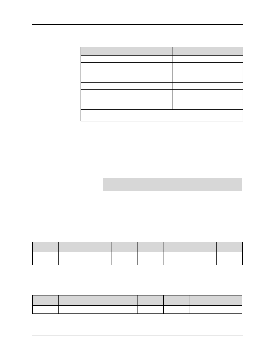
8-40
Mindspeed TechnologiesTM
500238B
Advance Information
Register Description
CX29503 Data Sheet
ACTIVE
Framer Active--The offline framer transitions to its ACTIVE state in response to an RFORCE
or TFORCE reframe request from the processor or in response to RLOF or TLOF reframe
request from an online framer. The offline framer remains ACTIVE until alignment is found
(FOUND), search is aborted [see RABORT, addr: 040; or TABORT, addr: 071], search
reaches its time-out interval (TIMEOUT), or all possible frame candidates are eliminated
(INVALID).
0 = offline framer inactive; search completed, aborted or timed-out
1 = offline framer actively searching for alignment
RX/TXN
RX/TX Reframe Operation--Indicates in which direction the offline framer is actively
searching or most recently searched for frame alignment. RX/TXN status is updated when the
offline framer transitions to its ACTIVE state in response to a reframe request.
0 = search data from the TSB interface
1 = search data from the Receive Line Interface unit
0x18--Programmable Input/Output (PIO)
This register must be written to 0x5A on initialization and maintained at that value.
0x19--Programmable Output Enable (POE)
This register must be written to 0x00 on initialization and maintained at that value.
Table 8-12. Maximum Average Reframe Time (MART) and Framer Time-Out
Framer Mode
MART
TIMEOUT (addr: 017)
Ft
3.5 ms
12 ms
±
1 bit
SF
3.5 ms
12 ms
±
1 bit
SF + JYEL
4.5 ms
12 ms
±
1 bit
ESF
10.0 ms
24 ms
±
1 bit
ESF + CRC
15.0 ms
24 ms
±
1 bit
ESF + MIMIC
15.0 ms
24 ms
±
1 bit
FAS
0.5 ms
8 ms
±
125
µ
s
MFAS
10.0 ms
8 ms
±
125
µ
s
GENERAL NOTE:
MART is defined (per Telcordia TA-TSY-000278) as the difference between the time that a
known good pseudo-random DS1 input is applied and the time that a valid DS0 signal is observed at the output.
NOTE:
RFORCE or TFORCE do not change current RLOF or TLOF status. RFORCE or TFORCE
is cleared by a framer transition to ACTIVE.
7
6
5
4
3
2
1
0
RMSYNC_EN
(set to 0)
RDL_IO
(set to 1)
TMSYNC_EN
(set to 0)
TDL_IO
(set to 1)
RFSYNC_IO
(set to 1)
RMSYNC_IO
(set to 0)
TFSYNC_IO
(set to 1)
TMSYNC_IO
(set to 0)
7
6
5
4
3
2
1
0
--
--
TDL_OE
RDL_OE
INDY_OE
TCKO_OE
--
--

500238B
Mindspeed TechnologiesTM
8
-
41
Advance Information
CX29503 Data Sheet
Register Description
8.3.2.5
Digital Receiver Registers
0x40--Receiver Configuration (RCR0)
RAMI
Receive AMI Encoded Input--Disables ZCS encoding/decoding for AMI formatted RTIP/
RRING receive signals. The CX29503 device does not include a ZCS encoder/decoder. This
bit must be set for CX29503.
0 = receive B8ZS/HDB3 line format
1 = receive AMI line format
RABORT
Abort/Disable RX Offline Framer--When set, the offline framer ignores reframe requests
from the online framer (RLOF) and aborts any in-progress RLOF reframe request. LOF status
[RLOF; addr: 047] is not affected. While RABORT remains set, the offline framer responds
only to processor-forced reframes (RFORCE). This allows the processor to manually control
reframe criteria and prevent changes in the current receive frame alignment. RABORT is
typically set only during unchannelized operation.
0 = normal framer operation
1 = framer disabled
RFORCE
Force RX Reframe--Forces the offline framer to perform a single reframe according to a
selected receive framer mode. RFORCE is automatically cleared when the offline framer
acknowledges the request [FSTAT; addr: 017]. The processor does not typically need to force
reframe since the online framer reframe request (RLOF) is active whenever reframe criteria
(RLOFD≠RLOFA) is met. However, the processor may force reframe if frame or CRC error
ratios indicate that the framer might have aligned to a duplicated frame alignment pattern.
0 = no effect
1 = force RX reframe
RLOFD≠RLOFA
RX Reframe Criteria--Determines the number of frame errors that the online framer must
detect before declaring LOS alignment [ALM1; addr: 047]. See Receive Framer mode
[RFRAME; addr: 001] and
Table 8-5
to find which frame bits are monitored.
7
6
5
4
3
2
1
0
RAMI
RABORT
RFORCE
RLOFD
RLOFC
RLOFB
RLOFA
RESERVED
Table 8-13. Reframe Criteria
T1/E1N
RLOFD≠RLOFA
Reframe Criteria
0
0100
3 consecutive FAS errors
0
1100
3 consecutive FAS or 915 CRC errors
1
0001
2 out of 4 F-bit errors
1
0010
2 out of 5 F-bit errors
1
0100
2 out of 6 F-bit errors
GENERAL NOTE:
Other RLOFD≠RLOFA combinations are invalid. RAIS and RLOF statuses are
disabled if RLOFD≠RLOFA equals all 0s.

8-42
Mindspeed TechnologiesTM
500238B
Advance Information
Register Description
CX29503 Data Sheet
0x41--Receive Test Pattern Configuration (RPATT)
RESEED
Reseed PRBS Sync Detector (auto-clear)--If BSTART is active-high, writing a 1 to RESEED
forces the PRBS sync detector to reseed and search for test pattern sync [PSYNC; addr: 00B].
The reseed and search algorithm remains active until test pattern sync is found.
0 = no effect
1 = reseed and search for test pattern sync
BSTART
Enable PRBS Detector and Start Counting PRBS Bit Errors--BERR [addr: 058, 059]
counting is enabled when BSTART is active-high, and pattern sync is found
[PSYNC = 1; addr: 00B]. Otherwise, BERR counter holds its present value until cleared by a
processor read.
0 = PRBS detector disabled and BERR stops counting
1 = enable PRBS detector and BERR counter
FRAMED
PRBS Framed--When set, PRBS test pattern bits are not checked during F-bit locations in T1
mode or TS0 locations in E1 mode. Otherwise, test patterns are checked in all T1/E1 bit
locations. FRAMED, ZLIMIT, and RPATT establish the test pattern measurement type as
listed in
Table 8-14
.
ZLIMIT
PRBS Zero Limit--Determines the number of consecutive 0s allowed within the selected
PRBS test pattern. See
Table 8-14
for test pattern measurement options.
7
6
5
4
3
2
1
0
--
--
RESEED
BSTART
FRAMED
ZLIMIT
RPATT[1]
RPATT[0]
Table 8-14. Receive PRBS Test Pattern Measurements
FRAMED
ZLIMIT
RPATT
Test Pattern Measurements
Inversion
0
0
00
Unchannelized 2
11
No
0
0
01
Unchannelized 2
15
Yes
0
0
10
Unchannelized 2
20
No
0
0
11
Unchannelized 2
23
Yes
0
1
00
Unchannelized 2
11
with 7 zero limit
No
0
1
01
Unchannelized 2
15
with 7 zero limit (nonstandard)
No
0
1
10
Unchannelized 2
20
with 14 zero limit (QRSS/QRS/QRTS)
No
0
1
11
Unchannelized 2
23
with 14 zero limit (nonstandard)
No
1
0
00
Framed 2
11
No
1
0
01
Framed 2
15
Yes
1
0
10
Framed 2
20
No
1
0
11
Framed 2
23
Yes
1
1
00
Framed 2
11
with 7 zero limit
No
1
1
01
Framed 2
15
with 7 zero limit (nonstandard)
No
1
1
10
Framed 2
20
with 14 zero limit (QRSS/QRS/QRTS)
No
1
1
11
Framed 2
23
with 14 zero limit (nonstandard)
No
500238B
Mindspeed TechnologiesTM
8
-
43
Advance Information
CX29503 Data Sheet
Register Description
RPATT[1:0]
PRBS Test Pattern--Selects one of four PRBS test pattern lengths used to measure the
received bit error ratio during out-of-service testing. See
Table 8-14
for test pattern
measurement options. PRBS test patterns used by RPATT [addr: 041] and TPATT [addr: 076]
are defined in ITU Standards O.151 and O.152 to use either inverted or non-inverted data.
Standard data inversion is used for selected PRBS test patterns unless ZLIMIT is enabled, in
which case the test pattern always uses non-inverted data.
0x42--Receive Loopback Code Detector Configuration (RLB)
Unused bits should be written to 0.
DN_LEN[1:0]
Loopback Deactivate Code Length--Selects the number of loopback pattern bits from LBD
[addr: 044] that are compared to received data. This is done to determine whether a Loopback
Deactivate Code [LOOPDN; addr: 048] has been detected. LOOPDN is recovered if the
received data pattern contains fewer than 63 bit errors in a 24-ms period, or lost if 64 or more
bit errors are detected in a subsequent 24-ms period. F-bits that overwrite or are inserted into
the loopback pattern are not counted as bit errors. Accurate code detection is provided on lines
with up to 1
-3
BER.
UP_LEN[1:0]
Loopback Activate Code Length--Selects the number of loopback pattern bits from LBA
[addr: 043] that are compared to received data. This is done to determine whether a Loopback
Activate Code [LOOPUP; addr: 048] has been detected. LOOPUP is recovered if the received
data pattern contains fewer than 63 bit errors in a 24-ms period, or lost if 64 or more bit errors
are detected in a subsequent 24-ms period. F-bits that overwrite or are inserted into the
loopback pattern are not counted as bit errors. Accurate code detection is provided on lines
with up to 1
-3
BER.
7
6
5
4
3
2
1
0
--
--
--
--
DN_LEN[1]
DN_LEN[0]
UP_LEN[1]
UP_LEN[0]
DN_LEN
LBD Length
00
4 bits
01
5 bits
10
6 bits
11
7 bits
UP_LEN
LBA Length
00
4 bits
01
5 bits
10
6 bits
11
7 bits

8-44
Mindspeed TechnologiesTM
500238B
Advance Information
Register Description
CX29503 Data Sheet
0x43--Loopback Activate Code Pattern (LBA)
Unused bits should be written to 0.
LBA[1]
First bit expected of LOOPUP pattern
LBA[2]
Second bit expected of LOOPUP pattern
LBA[3]
Third bit expected of LOOPUP pattern
LBA[4]
Fourth bit expected--Last bit if UP_LEN selects a 4-bit pattern
LBA[5]
Fifth bit expected--Last bit if UP_LEN selects a 5-bit pattern
LBA[6]
Sixth bit expected--Last bit if UP_LEN selects a 6-bit pattern
LBA[7]
Seventh bit expected--Last bit if UP_LEN selects a 7-bit pattern
0x44--Loopback Deactivate Code Pattern (LBD)
Unused bits should be written to 0.
LBD[1]
First bit expected of LOOPDN pattern
LBD[2]
Second bit expected of LOOPDN pattern
LBD[3]
Third bit expected of LOOPDN pattern
LBD[4]
Fourth bit expected--Last bit if DN_LEN selects a 4-bit pattern
LBD[5]
Fifth bit expected--Last bit if DN_LEN selects a 5-bit pattern
LBD[6]
Sixth bit expected--Last bit if DN_LEN selects a 6-bit pattern
LBD[7]
Seventh bit expected--Last bit if DN_LEN selects a 7-bit pattern
7
6
5
4
3
2
1
0
LBA[1]
LBA[2]
LBA[3]
LBA[4]
LBA[5]
LBA[6]
LBA[7]
--
7
6
5
4
3
2
1
0
LBD[1]
LBD[2]
LBD[3]
LBD[4]
LBD[5]
LBD[6]
LBD[7]
--

500238B
Mindspeed TechnologiesTM
8
-
45
Advance Information
CX29503 Data Sheet
Register Description
0x45--Receive Alarm Signal Configuration (RALM)
Unused or reserved bits should be written to 0.
AUTO_AIS
Automatically inserts an AIS toward the system when the line reports AIS or LOF in DS1
mode or OOF in E1 mode. This bit was added to the CX29503 DS1/E1 framer
implementation.
DIS_LCV
For the CX92503, this bit is not applicable and must be set to 1 to disable LCV indication and
counting.
FS_NFAS
Include FS/NFAS in FERR and FRED--Selects whether Fs bit errors (T1) or NFAS Bit 2
errors (E1) are counted as frame errors [FERR; addr: 050, 051]. Further selects whether LOF
alignment [FRED; addr: 049] includes Fs or NFAS bit errors as part of the detection criteria.
0 = FERR and FRED do not include FS/NFAS
1 = FERR and FRED include FS/NFAS
YEL_INTEG
Enable Yellow Alarm Integration--When set, both the Receive Frame and Multiframe Yellow
alarms [RYEL and RMYEL; addr: 047] are integrated, as described in
Table 8-15
(per the
selected framer mode). RYEL and RMYEL interrupt statuses [ISR7; addr: 004] are similarly
affected.
0 = normal RYEL and RMYEL status
1 = integrated RYEL and RMYEL status
7
6
5
4
3
2
1
0
AUTO_AIS
DIS_LCV
FS_NFAS
RESERVED
YEL_INTEG
RLOF_INTEG
RESERVED
RESERVED
NOTE:
The number of Fs bit locations checked also depends on the JYEL framer mode.
Table 8-15. Receive Yellow Alarm Set and Clear Criteria <tableContinuation>(1 of 2)
Mode
Set and Clear Criteria
Y0
Set for 4 frames (500
µ
s) if 2 consecutive NFAS frames each contain TS0 bit 3 = 1.
Cleared for 4 frames if 2 consecutive NFAS frames each contain TS0 bit 3 = 0.
Y0_INT
Set for 16 multiframes (24 ms) if every NFAS frame contains TS0 bit 3 = 1. Cleared
for 16 multiframes if 1 or more NFAS frames contain TS0 bit 3 = 0.
Y16
Set for 2 multiframes (4 ms) if frame 0 in 2 consecutive multiframes contains TS16
bit 6 = 1. Cleared for 2 multiframes if frame 0 in 2 consecutive multiframes
contains TS16 bit 6 = 0.
Y16_INT
Set for 16 multiframes (24 ms) if every frame 0 contains TS16 bit 6 = 1. Cleared for
16 multiframes if at least 1 frame 0 contains TS16 bit 6 = 0.
YB2
Set for 1 frame (125
µ
s) if all 24 time slots contain bit 2 = 0. Cleared for 1 frame if
1 or more time slots contain bit 2 = 1.
YB2_INT
Set for 192 frames (24 ms) if less than 15 time slots contain bit 2 = 0. Cleared for
192 frames if 15 or more time slots contain bit 2 = 1.
YJ
Set for 1 multiframe (1.5 ms) if frame 12 contains Fs bit = 1. Cleared for 1
multiframe if frame 12 contains Fs bit = 0.
YJ_INT
Set for 16 multiframes (24 ms) if every frame 12 contains Fs bit = 1. Cleared for 16
multiframes (24 ms) if at least 1 frame 12 contains Fs bit = 0.

8-46
Mindspeed TechnologiesTM
500238B
Advance Information
Register Description
CX29503 Data Sheet
RLOF_INTEG
Enable RLOF Integration--When set, the receive LOF status [RLOF; addr: 047] is integrated
for 2.0≠2.5 seconds during T1 framer modes (not applicable to E1 modes). RLOF interrupt
status [ISR7; addr: 004] is also integrated. However, receive framer status in ALM3
[addr: 049], LOF count [FRED[3:0]; addr: 05A], and RLOF counter overflow
[ISR4; addr: 007] are unaffected.
0 = normal RLOF status
1 = integrated RLOF [addr: 047] status
Y24
Set for 1 frame (125
µ
s) if TS24 contains bit 6 = 0. Cleared for 1 frame if TS24
contains bit 6 = 1.
Y24_INT
Set for 192 frames (24 ms) if every TS24 bit 6 = 0. Cleared for 192 frames if at
least 1 TS24 bit 6 = 1.
YF
Set for 32 frames (4 ms) if 16 FDL bits contain yellow alarm priority code word
pattern (00FFh). Cleared for 32 frames if 16 FDL bits do not contain a yellow alarm
priority code word pattern.
YF_INT
Set upon reception of 16 FDL bits matching yellow alarm priority code word and
remains set as long as the code word pattern is not interrupted for greater than 100
ms. Cleared when the yellow alarm priority code word is not present for more than
100 ms (26 missing code words = 104 ms).
Table 8-15. Receive Yellow Alarm Set and Clear Criteria <tableContinuation>(2 of 2)
Mode
Set and Clear Criteria

500238B
Mindspeed TechnologiesTM
8
-
47
Advance Information
CX29503 Data Sheet
Register Description
0x46--Alarm/Error/Counter Latch Configuration (LATCH)
Unused bits should be written to 0.
STOP_CNT
Stop Error Count during RLOF/RLOS/RAIS--If enabled, error count registers [addr: 050≠
057] are suspended at their present values during any receive LOF (RLOF), LOS (RLOS), or
all 1s (RAIS) alarm condition. STOP_CNT does not affect the counting of test pattern errors
[BERR; addr: 058, 059] or alarm events [AERR; addr: 05A]. The occurrence of a red or AIS
Carrier Group Alarm (CGA) will inhibit further processing of all other performance
parameters (i.e., BER, errored seconds, SLIPS, etc.). However, a CGA caused by a yellow
alarm will not inhibit further alarm or performance monitoring.
0 = continue error count during alarms
1 = stop error count during alarms
LATCH_CNT
Enable OneSec Latching of Counters--Determines the interval for which error counts remain
held in all count registers [addr: 050≠057]. LATCH_CNT must be active in T1 mode whenever
automatic one-second performance report messaging [AUTO_PRM; addr: 0AA] is enabled.
When LATCH_CNT is inactive, the processor read of the LSB register reports the current LSB
error count, it latches the current MSB error count to the MSB register, and it clears the LSB.
Subsequently, reading the MSB register reports the current latched MSB error count and then
clears the MSB.
LATCH_ERR
Enable OneSec Latching of Errors--Determines the interval for which latched active errors
are held in error interrupt [ISR5; addr: 006] and pattern interrupt [ISR0; addr: 00B] status.
7
6
5
4
3
2
1
0
--
--
--
--
STOP_CNT
LATCH_CNT
LATCH_ERR
LATCH_ALM
NOTE:
LATCH_CNT being active during E1 mode prevents the processor from using RLOF
counter overflow [addr: 007] as a 128 ms MFAS time-out.
Table 8-16. Latch Counter intervals
LATCH_CNT
Count Latched
Count Hold Time
0
Never
Until read clear
1
OneSec interval
OneSec interval
Table 8-17. Error Latching Options
IER
LATCH_ERR
ISR Latched
ISR Hold Time
0
0
Rising edge event
Until read clear
0
1
Rising edge event
OneSec interval
1
X
Rising edge event
Until read clear
8-48
Mindspeed TechnologiesTM
500238B
Advance Information
Register Description
CX29503 Data Sheet
LATCH_ALM
Enable OneSec Latching of Alarms--Determines the interval for which latched active alarms
remain held in alarm interrupt status [ISR7, ISR6; addr: 004, 005].
0x47--Alarm 1 Status (ALM1)
ALM1 reports the current status of receive alarms. Any change in the current status activates the corresponding
interrupt status bit [ISR7; addr: 004].
Unused bits are reserved and should be written to 0.
RMYEL
Receive Multiframe Yellow Alarm--Real-time or integrated RMYEL status depends on the
selected framer mode and the yellow alarm integration mode [YEL_INTEG; addr: 045].
See
Table 8-19
for information on the parameter reported by RMYEL. See
Table 8-5
for the
mode summary and
Table 8-15
for parameter definitions.
0 = no alarm
1 = receive multiframe yellow alarm
RYEL
Receive Yellow Alarm--Real-time or integrated RYEL status depends on selected receive
framer mode and yellow alarm integration mode [YEL_INTEG; addr: 045]. See
Table 8-19
for
information on the parameter reported by RYEL. See
Table 8-5
for the mode summary and
Table 8-15
for parameter definitions.
0 = no alarm
1 = receive yellow alarm
RAIS
Receive Alarm Indication Signal--Criteria for detection and clearance of RAIS per ITU G.775
and ANSI T1.231.
Table 8-18. Alarm Latching Options
IER
LATCH_ALM
ISR Latched
ISR Hold Time
0
0
Rising edge or transition
Until read clear
0
1
Rising edge or transition
OneSec interval
1
X
Rising edge or transition
Until read clear
GENERAL NOTE:
Interrupt type determines rising edge or transition event.
7
6
5
4
3
2
1
0
RMYEL
RYEL
--
RAIS
RESERVED
RESERVED
RLOF
RESERVED
Table 8-19. Receive Yellow Alarm
Receive Framer
Mode
YEL_INTEG = 0
YEL_INTEG = 1
RYEL
RMYEL
RYEL
RMYEL
FT/SF
YB2
--
YB2_INT
--
JYEL
YJ
--
YJ_INT
--
ESF
YB2
YF
YB2_INT
YF_INT
FAS
Y0
--
Y0_INT
--
GENERAL NOTE:
The last known frame alignment is used to locate and monitor yellow alarms.
Therefore, RYEL and RMYEL will not accurately report alarms during receive loss of frame
alignment [RLOF; addr: 047].
500238B
Mindspeed TechnologiesTM
8
-
49
Advance Information
CX29503 Data Sheet
Register Description
RLOF
Receive Loss of Frame Alignment--Real-time or integrated RLOF status depends on selected
receive framer mode, out-of-frame criteria [RLOFA≠RLOFD; addr: 040], and integration
mode [RLOF_INTEG; addr: 045]. In the CX28394/5/8 Data Sheet, see
Tables A-1
≠
A-6
in
Appendix A to find which frame bits are monitored. See
Table 8-6
for the loss/recovery
criteria for frame alignment loss/recovery criteria during the selected mode. During E1 mode,
RLOF indicates logically ORed status of FAS/MFAS alignment machines from which
individual alignment status is reported separately in FRED/MRED [addr: 049].
0 = no alarm
1 = receive loss of frame alignment
0x48--Alarm 2 Status (ALM2)
Reports the real-time status of transmit alarms and inband loopback code word detectors. Any change in the
current status activates the corresponding interrupt status bit [ISR6; addr: 005].
Unused and reserved bits should be written to 0.
LOOPDN
Inband Loopback Deactivate--Reports detection or loss of an inband loopback code which
matches the programmed LOOPDN code [LBD; addr: 044].
0 = no inband code (or lost)
1 = LOOPDN code detected
LOOPUP
Inband Loopback Activate--Reports detection or loss of an inband loopback code which
matches the programmed LOOPUP code [LBA; addr: 043].
0 = no inband code (or lost)
1 = LOOPUP code detected
Table 8-20. Receive Alarm Indication Signal (RAIS)
Mode
RAIS
Set/Clear Criteria
E1
0
Cleared if 2 consecutive double frames (500
µ
s) each contain 3 or more 0s
out of 512 bits or FAS alignment is recovered [FRED = 0; addr: 049].
E1
1
Set if 2 consecutive double frames each contain 2 or fewer 0s out of 512
bits and FAS alignment is lost [FRED = 1; addr: 049].
T1
0
Cleared if data received for a period of 3 ms contains 5 or more 0s out of
4,632 bits or frame alignment is recovered [FRED = 0; addr: 049].
T1
1
Set if data received for a period of 3 ms contains 4 or fewer 0s out of 4,632
bits and frame alignment is lost [FRED = 1; addr: 049].
7
6
5
4
3
2
1
0
LOOPDN
LOOPUP
--
--
RESERVED
--
RESERVED
--
8-50
Mindspeed TechnologiesTM
500238B
Advance Information
Register Description
CX29503 Data Sheet
0x49--Alarm 3 Status (ALM3)
Reports real-time status of the receive framer (not affected by OneSec latch mode), and miscellaneous latched
error status (SEF). Any change of the logical OR of FRED or MRED status activates the RLOF interrupt
[ISR7; addr: 004]. See
Table 8-6
, to find the criteria for loss/recovery of frame alignment.
Unused and reserved bits should be written to 0.
SEF
Severely Errored Frame (SEF)--SEF is latched active-high and cleared by a processor read.
Criteria for detection and clearance of SEF is per ANSI T1.231.
MRED
Loss of MFAS Alignment--Real-time status of MFAS alignment machine. MRED is
applicable if MFAS is enabled, otherwise MRED is 0.
0 = recovery of MFAS alignment
1 = loss of MFAS alignment
FRED
Loss of T1/FAS Alignment--Real-time status of basic frame alignment machine.The FRED
alarm counter [AERR; addr: 05A] increments for each low-to-high FRED transition.
0 = recovery of frame alignment
1 = loss of frame alignment
LOF[1:0]
Reason for Loss Of Frame Alignment--LOF status is latched whenever FRED reports a loss
of frame alignment and remains held at the latched value until the next loss of frame
alignment.
7
6
5
4
3
2
1
0
--
RESERVED
SEF
RESERVED
MRED
FRED
LOF[1]
LOF[0]
Table 8-21. SEF Criteria
Mode
SEF Criteria
E1
Set if 2 or more (FAS or NFAS) errors detected out of 6 frames (FAS + NFAS, or 2 FAS, or
2 NFAS errors, etc.)
FT/SF
Set if 2 or more Ft errors are detected out of 3 Ft bits
ESF
Set if 2 or more FPS errors detected out of 6 FPS bits
Table 8-22. Loss Of Frame Alignment Criteria
LOF[1:0]
LOF Criteria
00
Three consecutive FAS pattern errors
01
Three consecutive NFAS pattern errors
10
915 or more CRC4 errors out of 1,000 blocks checked
11
Eight ms timeout while searching for MFAS

500238B
Mindspeed TechnologiesTM
8
-
51
Advance Information
CX29503 Data Sheet
Register Description
8.3.2.6
Performance Monitoring Registers
If the counter overflow interrupt [IER4; addr: 00F] is enabled for the respective Performance Monitoring
counter, the counter is allowed to roll over after reaching its maximum count value. If the overflow interrupt is
disabled, the counter will hold its maximum value upon saturation. Refer also to LATCH [addr: 046] for a
description of one-second latched counter operation. The processor must read the LSB before reading the MSB
of each multibyte counter.
0x50--Framing Bit Error Counter LSB (FERR)
FERR[7:0]
Ft/Fs/FPS/FAS Error Count
0x51--Framing Bit Error Counter MSB (FERR)
If LATCH_CNT [addr: 046] is inactive, reading FERR [addr: 051] clears the entire FERR[11:0] count value.
FERR[11:8]
Ft/Fs/FPS/FAS Error Count
0x52--CRC Error Counter LSB (CERR)
CERR[7:0]
CRC6/CRC4 Error Count
0x53--vCRC Error Counter MSB (CERR)
If LATCH_CNT [addr: 046] is inactive, reading CERR [addr: 053] clears the entire CERR[9:0] count value.
CERR[9:8]
CRC6/CRC4 Error Count
7
6
5
4
3
2
1
0
FERR[7]
FERR[6]
FERR[5]
FERR[4]
FERR[3]
FERR[2]
FERR[1]
FERR[0]
15
14
13
12
11
10
9
8
0
0
0
0
FERR[11]
FERR[10]
FERR[9]
FERR[8]
7
6
5
4
3
2
1
0
CERR[7]
CERR[6]
CERR[5]
CERR[4]
CERR[3]
CERR[2]
CERR[1]
CERR[0]
15
14
13
12
11
10
9
8
0
0
0
0
0
0
CERR[9]
CERR[8]

8-52
Mindspeed TechnologiesTM
500238B
Advance Information
Register Description
CX29503 Data Sheet
0x56--Far End Block Error Counter LSB (FEBE)
FEBE[7:0]
FEBE Count (applicable only in E1 mode)
0x57--Far End Block Error Counter MSB (FEBE)
If LATCH_CNT [addr: 046] is inactive, reading FEBE [addr: 056, 057] clears the entire FEBE[9:0] count value.
FEBE[9:8]
FEBE Count (applicable only in E1 mode)
0x58--PRBS Bit Error Counter LSB (BERR)
Reading BERR transfers the most recent 12-bit count from the internal PRBS error counter to BERR[11:0],
then clears the internal error counter without affecting the reported BERR[11:0] value. Subsequent reads of
BERR MSB [addr: 059] report the BERR [11:8] count value latched when BERR LSB was last read.
BERR[7:0]
BERR Count (applicable only for test patterns)
0x59--PRBS Bit Error Counter MSB (BERR)
BERR[11:8]
BERR Count (suspended if BSTART = 0)
7
6
5
4
3
2
1
0
FEBE[7]
FEBE[6]
FEBE[5]
FEBE[4]
FEBE[3]
FEBE[2]
FEBE[1]
FEBE[0]
15
14
13
12
11
10
9
8
0
0
0
0
0
0
FEBE[9]
FEBE[8]
7
6
5
4
3
2
1
0
BERR[7]
BERR[6]
BERR[5]
BERR[4]
BERR[3]
BERR[2]
BERR[1]
BERR[0]
15
14
13
12
11
10
9
8
0
0
0
0
BERR[11]
BERR[10]
BERR[9]
BERR[8]

500238B
Mindspeed TechnologiesTM
8
-
53
Advance Information
CX29503 Data Sheet
Register Description
0x5A--SEF/FRED/COFA Alarm Counter (AERR)
Reading AERR clears the SEF[1:0], COFA[1:0], and FRED[3:0] count values.
FRED[3:0]
Receive Loss of Basic Frame Alignment Count--Increments for each occurrence of FRED
[ALM3; addr: 049]. The 4-bit count is large enough to count more than 100 ms worth of
MFAS time-out intervals (8 ms each) during E1 modes. The processor may therefore use the
FRED counter overflow interrupt to indicate that a receive MFAS alignment search has timed
out.
COFA[1:0]
Change of Frame Alignment Count--Increments each time the offline framer generates a
reframe pulse that aligns the receiver time base to a new bit position.
SEF[1:0]
Severely Errored Frame Count--Increments for each occurrence of SEF [ALM3; addr: 049].
7
6
5
4
3
2
1
0
FRED[3]
FRED[2]
FRED[1]
FRED[0]
COFA[1]
COFA[0]
SEF[1]
SEF[0]

8-54
Mindspeed TechnologiesTM
500238B
Advance Information
Register Description
CX29503 Data Sheet
8.3.2.7
Receive Sa-Byte Buffers
Five receive Sa-Byte buffers [RSA4≠RSA8] are double-buffered. All 5 registers are updated with the Sa bits
received in TS0 of odd frames at each receive multiframe interrupt [RMF; addr: 008]. Bit 0 of all RSA registers
contains data from Frame 1, Bit 1 contains data from Frame 3, Bit 2 contains data from Frame 5, etc. This gives
the processor a full 2 ms after RMF interrupt to read any Sa-Byte buffer before the buffer content changes. The
processor should ignore RSA buffer contents at all times during T1 mode and also when the receiver reports
loss-of-FAS alignment [FRED=1; addr: 049] in E1 mode.
0x5B--Receive Sa4 Byte Buffer (RSA4)
RSA4[7]
Sa4 bit received in Frame 15
RSA4[6]
Sa4 bit received in Frame 13
RSA4[5]
Sa4 bit received in Frame 11
RSA4[4]
Sa4 bit received in Frame 9
RSA4[3]
Sa4 bit received in Frame 7
RSA4[2]
Sa4 bit received in Frame 5
RSA4[1]
Sa4 bit received in Frame 3
RSA4[0]
Sa4 bit received in Frame 1
0x5C--Receive Sa5 Byte Buffer (RSA5)
RSA5[7]
Sa5 bit received in Frame 15
RSA5[6]
Sa5 bit received in Frame 13
RSA5[5]
Sa5 bit received in Frame 11
RSA5[4]
Sa5 bit received in Frame 9
RSA5[3]
Sa5 bit received in Frame 7
RSA5[2]
Sa5 bit received in Frame 5
RSA5[1]
Sa5 bit received in Frame 3
RSA5[0]
Sa5 bit received in Frame 1
7
6
5
4
3
2
1
0
RSA4[7]
RSA4[6]
RSA4[5]
RSA4[4]
RSA4[3]
RSA4[2]
RSA4[1]
RSA4[0]
7
6
5
4
3
2
1
0
RSA5[7]
RSA5[6]
RSA5[5]
RSA5[4]
RSA5[3]
RSA5[2]
RSA5[1]
RSA5[0]

500238B
Mindspeed TechnologiesTM
8
-
55
Advance Information
CX29503 Data Sheet
Register Description
0x5D--Receive Sa6 Byte Buffer (RSA6)
RSA6[7]
Sa6 bit received in Frame 15
RSA6[6]
Sa6 bit received in Frame 13
RSA6[5]
Sa6 bit received in Frame 11
RSA6[4]
Sa6 bit received in Frame 9
RSA6[3]
Sa6 bit received in Frame 7
RSA6[2]
Sa6 bit received in Frame 5
RSA6[1]
Sa6 bit received in Frame 3
RSA6[0]
Sa6 bit received in Frame 1
0x5E--Receive Sa7 Byte Buffer (RSA7)
RSA7[7]
Sa7 bit received in Frame 15
RSA7[6]
Sa7 bit received in Frame 13
RSA7[5]
Sa7 bit received in Frame 11
RSA7[4]
Sa7 bit received in Frame 9
RSA7[3]
Sa7 bit received in Frame 7
RSA7[2]
Sa7 bit received in Frame 5
RSA7[1]
Sa7 bit received in Frame 3
RSA7[0]
Sa7 bit received in Frame 1
7
6
5
4
3
2
1
0
RSA6[7]
RSA6[6]
RSA6[5]
RSA6[4]
RSA6[3]
RSA6[2]
RSA6[1]
RSA6[0]
7
6
5
4
3
2
1
0
RSA7[7]
RSA7[6]
RSA7[5]
RSA7[4]
RSA7[3]
RSA7[2]
RSA7[1]
RSA7[0]

8-56
Mindspeed TechnologiesTM
500238B
Advance Information
Register Description
CX29503 Data Sheet
0x5F--Receive Sa8 Byte Buffer (RSA8)
RSA8[7]
Sa8 bit received in Frame 15
RSA8[6]
Sa8 bit received in Frame 13
RSA8[5]
Sa8 bit received in Frame 11
RSA8[4]
Sa8 bit received in Frame 9
RSA8[3]
Sa8 bit received in Frame 7
RSA8[2]
Sa8 bit received in Frame 5
RSA8[1]
Sa8 bit received in Frame 3
RSA8[0]
Sa8 bit received in Frame 1
7
6
5
4
3
2
1
0
RSA8[7]
RSA8[6]
RSA8[5]
RSA8[4]
RSA8[3]
RSA8[2]
RSA8[1]
RSA8[0]

500238B
Mindspeed TechnologiesTM
8
-
57
Advance Information
CX29503 Data Sheet
Register Description
8.3.2.8
Digital Transmitter Registers
0x70--Transmit Framer Configuration (TCR0)
TCR0 selects the offline framer's criteria for recovery of transmit frame alignment and determines the output of
the transmit frame and alarm formatters overhead bits. In addition, TCR0 works in conjunction with TCR1
[addr: 071] and TFRM [addr: 072] to select the transmit online frame monitor's criteria for LOF alignment and
which overhead bits are supplied by the transmit frame and alarm formatters.
Unused bits are reserved and should be written to 0.
EXMOP_EN
Enable External MOP--Overwrites the currently active BOP data with the external MOP data.
TINCF
Transmit CRC6 includes F-bit--Determines if the F-bit is included in the CR6 remainder
calculation in T1 mode (T1/E1N = 1). This bit is ignored in E1 mode (T1/E1N = 0).
0 = T1 ESF CRC6 calculation is performed on the transmit data including a 1 in place
of the F-bit
1 = T1 ESF CRC6 calculation is performed on the transmit data including the F-bit
TFRAME[3:0]
The Frame formatter generates Ft, Fs, FPS, FAS, MFAS, and CRC bits. The Alarm formatter
generates YB2, YJ, Y0, and Y16 bits. Frame and alarm overhead formats are selected by
TFRAME[3:0] and T1/E1N settings as given in
Tables 8-23
and
8-24
. Each yellow alarm is
capable of being generated manually, automatically [TALM; addr: 075], or bypassed
[INS_MYEL; addr: 072].
The Frame formatter does not generate Sa-bit overhead. These bits are either supplied by
the Sa-Byte registers [addr: 07B≠07F] or the TSB interface. The Frame formatter does not
generate FDL overhead. To insert FDL, the processor does one of the following:
∑ configures TDL1 [addr: 0AD] to operate over the F-bit channel during odd frames
[DL1_TS; addr: 0A4] and Automatic Performance Report messages
[AUTO_PRM; addr: 0AA]
∑ manually programs TDL1 to send each message
∑ sets up the external data link [DL3_TS; addr: 015] to use the TSB interface
7
6
5
4
3
2
1
0
--
--
EXMOP_EN
TINCF
TFRAME[3]
TFRAME[2]
TFRAME[1]
TFRAME[0]
Table 8-23. E1 Transmit Framer Modes (T1/E1N = 0)
TFRAME
Framer Mode
TS0 Overhead Insertion
Yellow Alarms
MFAS
FEBE
CRC4
FAS
YEL
MYEL
00XX
FAS only
1s
1s
1s
Yes
Y0
--
01XX
FAS + CRC
Yes
Yes
Yes
Yes
Y0
--

8-58
Mindspeed TechnologiesTM
500238B
Advance Information
Register Description
CX29503 Data Sheet
0x71--Transmitter Configuration (TCR1)
Reserved bits should be written to 0.
TNRZ
For the CX92503, this bit is not applicable and must be set to 1 to disable encoding.
TABORT
For the CX92503, this bit is not applicable and must be set to 1 to disable the offline framer
from responding to disabled reframe requests (TLOF).
0x72--Transmit Frame Format (TFRM)
TFRM controls the insertion of overhead bits generated by transmit frame and alarm formatters.
Unused bits should be written to 0.
INS_MYEL
Insert Multiframe Yellow Alarm--Applicable to E1 modes only. Enables the alarm formatter
to output the Y16 Multiframe Yellow Alarm. Once enabled, TMYEL and AUTO_MYEL
[addr: 075] control the alarm output state. This bit must be set to 0 in T1 modes.
0 = do not insert multiframe yellow alarm
1 = insert multiframe yellow alarm
INS_YEL
The alarm formatter outputs yellow alarms YB2 or YJ during T1 modes, or Y0 during E1
modes. In ESF framed T1 mode, the YF Yellow Alarm is transmitted by programming the DL1
data link controller and by transmitting the appropriate Bit-Oriented Protocol (BOP) code
message. Once enabled, TYEL and AUTO_YEL [addr: 075] control the yellow alarm output
state. In E1 MFAS mode, this bit must be set to 1.
0 = do not insert yellow alarm
1 = insert yellow alarm
Table 8-24. T1 Transmit Framer Modes (T1/E1N = 1)
TFRAME
Framer Mode
F-bit Overhead Insertion
Yellow Alarms
Fs
FPS
CRC6
Ft
YEL
MYEL
0000
FT Only
1s
--
--
Yes
YB2
--
0100
SF
Yes
--
--
Yes
YB2
--
0101
SF + JYEL
Yes
--
--
Yes
YJ
--
0001
ESF + No CRC
--
Yes
1s
--
YB2
YF
1100
ESF + Mimic CRC
--
Yes
Yes
--
YB2
YF
1101
ESF + Force CRC
--
Yes
Yes
--
YB2
YF
7
6
5
4
3
2
1
0
TNRZ
(set to 1)
TABORT
(set to 1)
RESERVED
RESERVED
RESERVED
RESERVED
RESERVED
RESERVED
7
6
5
4
3
2
1
0
--
--
INS_MYEL
INS_YEL
INS_MF
INS_FE
INS_CRC
INS_FBIT

500238B
Mindspeed TechnologiesTM
8
-
59
Advance Information
CX29503 Data Sheet
Register Description
INS_MF
Insert Multiframe Alignment--The frame formatter outputs a 6-bit SF alignment pattern in T1
mode or a 6-bit MFAS alignment pattern in E1 mode. INS_MF should be set while TFRAME
(addr: 070) selects Fs (T1) or MFAS (E1) alignment.
0 = do not insert multiframe alignment
1 = insert multiframe alignment
INS_FE
Insert FEBE-- During E1 mode, the alarm formatter automatically outputs TS0 bit 1 of
Frame 13 (FEBE13) and Frame 15 (FEBE15) in response to received CRC4 errors. FEBE13 is
active-low for each received CRC4 error detected in SMF I. FEBE15 is active-low for each
received CRC4 error detected in SMF II. INS_FE should be set while TFRAME (addr: 070)
selects FEBE (E1) alignment.
0 = do not insert FEBE
1 = insert FEBE
INS_CRC
Insert Cyclic Redundancy Check--The frame formatter outputs the calculated CRC6 bits in
T1 mode or CRC4 bits in E1 mode.
0 = do not insert cyclic redundancy check
1 = insert cyclic redundancy check
INS_FBIT
Insert Terminal Framing--The frame formatter outputs a 2-bit Ft alignment pattern in
F-bits of odd frames (SF framing) or FPS framing pattern (ESF framing) during T1 modes--or
8-bit FAS/NFAS alignment pattern during E1 modes. INS_FBIT should be set while TFRAME
(addr: 070) selects Ft (T1, SF), FPS (T1, ESF), or FAS (E1) alignment.
0 = do not insert terminal framing
1 = insert terminal framing
8-60
Mindspeed TechnologiesTM
500238B
Advance Information
Register Description
CX29503 Data Sheet
0x73--Transmit Error Insert (TERROR)
Transmit error insertion capabilities are provided for system diagnostic, production test, and test equipment
applications. Writing a 1 to any TERROR bit injects a single occurrence of the respective error on the
transmitter output. Writing a 0 has no effect. Multiple transmit errors can be generated simultaneously. Injected
errors also affect data sent during a Framer Loopback [FLOOP; addr: 014].
Reserved bits should be written to 0.
TMERR
Inject Multiframe Error--Injects a single Fs (T1) or MFAS (E1) bit error. TMERR performs a
logical inversion of the next multiframe bit transmitted. The processor can pace writing to
TMERR to control which MFAS bit is errored.
0 = no effect
1 = inject multiframe error
TBERR
Inject PRBS Test Pattern Error--Injects a single PRBS error by logically inverting the next
PRBS generator output bit. The processor can pace writing to TBERR to create the desired bit
error ratio (up to 5
-3
if TBERR asserted 1/192 bits at every frame interrupt).
0 = no effect
1 = inject PRBS error
TCOFA
Inject Transmit COFA--Forces a 1-bit shift in the location of transmit frame alignment by
deleting 1 bit position from the transmit frame.
TCERR
Inject CRC Error--Injects a single CRC6 (T1) or CRC4 (E1) bit error. TCERR performs a
logical inversion of the next CRC bit transmitted. The processor can pace writing to TCERR to
control which CRC bit is errored.
0 = no effect
1 = inject CRC error
TFERR
Inject Frame Bit Error--Injects a single Ft, FPS, or FAS bit error depending on the selected
transmit framer mode. TFERR performs a logical inversion of the next frame bit transmitted.
The processor can pace writing to TFERR, to control which frame bit is errored.
0 = no effect
1 = inject frame error
0x74--Transmit Manual Sa-Byte/FEBE Configuration (TMAN)
7
6
5
4
3
2
1
0
RESERVED
TMERR
TBERR
Reserved
TCOFA
TCERR
TFERR
RESERVED
Table 8-25. Transmit COFA Injection Options
TCOFA
T1/E1N
Transmit COFA
0
X
No effect
1
0
Inhibit output of TS0 bit 1 for 1 frame
1
1
Inhibit output of F-bit for 1 frame
7
6
5
4
3
2
1
0
INS_SA[8]
INS_SA[7]
INS_SA[6]
INS_SA[5]
INS_SA[4]
FEBE_II
FEBE_I
TFEBE

500238B
Mindspeed TechnologiesTM
8
-
61
Advance Information
CX29503 Data Sheet
Register Description
INS_SA[8]
Manual Sa8-Byte Transmit (0-bypass)
INS_SA[7]
Manual Sa7-Byte Transmit (0-bypass)
INS_SA[6]
Manual Sa6-Byte Transmit (0-bypass)
INS_SA[5]
Manual Sa5-Byte Transmit (0-bypass)
INS_SA[4]
Manual Sa4-Byte Transmit (0-bypass)
FEBE_II
Transmit FEBE Frame 15
FEBE_I
Transmit FEBE Frame 13
TFEBE
Manual Transmit FEBE (Overrides INS_FE; addr: 072)--Provides a manual override for
FEBE bits that are normally sent by the alarm formatter [INS_FE; addr: 072]. When active,
FEBE_I controls the data output in TS0 bit 1 of Frame 13 (FEBE13) and FEBE_II controls the
data output in TS0 bit 1 of Frame 15 (FEBE15).
Table 8-26. Manual Transmit FEBE Options
INS_FE
TFEBE
FEBE[13]
FEBE[15]
Description
0
X
TPCMI
TPCMI
Bypass FEBE
1
0
SMF I
SMF II
Automatic FEBE
1
1
FEBE_I
FEBE_II Manual
FEBE
GENERAL NOTE:
Automatic FEBE insertion uses two separate CRC4 error signals from the receiver
to indicate SMF I and SMF II errors. Each error signal is latched and held for one full multiframe to
compensate for phase differences between receive and transmit multiframe timing.
8-62
Mindspeed TechnologiesTM
500238B
Advance Information
Register Description
CX29503 Data Sheet
0x75--Transmit Alarm Signal Configuration (TALM)
Unused and reserved bits should be written to 0.
AUTO_MYEL and
TMYEL
Manual and Automatic Transmit Multiframe Yellow Alarm--Manual mode sends the alarm
for as long as TMYEL is active. Automatic mode sends the alarm for the duration of a receive
loss of multiframe alignment [MRED; addr: 049].
AUTO_US_AIS and
US_TAIS
Manual and Automatic Upstream Transmit Alarm Indication Signal--When activated
manually (US_TAIS) or automatically (AUTO_US_AIS), the alarm formatter replaces all data
with an unchannelized, all-1s signal (AIS). This includes replacing data from the receiver
during Line Loopback [LLOOP; addr: 014]. Automatic mode sends the AIS for the duration of
Receive Loss Of Signal [RLOS; addr: 047].
Because the US_TAIS and AUTO_US_AIS bits effect the upstream data, these bits are only
applicable during a loopback condition. In normal operation, the AIS transmission is
automatically performed in the downstream direction using the AUTO_AIS bit in the Receive
Alarm Signal Condition register [addr: 045].
AIS transmission [TAIS, AUTO_AIS; addr: 075] does not affect transmit data that is looped
back to the receiver during Framer Loopback [FLOOP; addr: 014]. This allows both FLOOP
and LLOOP to be active simultaneously, during an LOS, without disrupting data in the framer
loopback path.
7
6
5
4
3
2
1
0
--
RESERVED
AUTO_MYEL
--
AUTO_US_AIS
TMYEL
--
US_TAIS
Table 8-27. Transmit Multiframe Yellow Alarm Options
INS_MYEL
TMYEL
AUTO_MYEL
Transmit Multiframe Yellow Alarm
0
X
X
Inactive
1
0
0
Inactive
1
0
1
Follows SRED status
1
1
X
Active
Table 8-28. Transmit Upstream Alarm Indication Signal
US_TAIS
US_AUTO_AIS
Transmit Data
0
0
Normal, no AIS
0
1
AIS during RLOS
1
X
Manual AIS
GENERAL NOTE:
Systems that transmit framed all 1s can utilize the inband loopback code generator
[TLB; addr: 077] to send all 1s in payload only.

500238B
Mindspeed TechnologiesTM
8
-
63
Advance Information
CX29503 Data Sheet
Register Description
0x76--Transmit Test Pattern Configuration (TPATT)
Unused bits should be written to 0.
TPSTART
Enable Test Pattern Transmission.
FRAMED
PRBS Framed--When set, the PRBS pattern does not overwrite framing bit positions and is
stopped during these bit periods. In T1 mode, the frame bit (every 193
rd
bit) is not overwritten.
If FRAMED is disabled, the test pattern is transmitted in all time slots.
ZLIMIT
Enable Zero Limit; 7/14 depending on pattern.
TPATT[1:0]
PRBS test patterns used by RPATT [addr: 041] and TPATT [addr: 076] are defined in the ITU
standards O.151 and O.152 to use either inverted or non-inverted data. Standard data inversion
is used for the selected PRBS test pattern unless ZLIMIT is enabled, in which case the test
pattern uses non-inverted data (see
Table 8-29
).
7
6
5
4
3
2
1
0
--
--
--
TPSTART
FRAMED
ZLIMIT
TPATT[1]
TPATT[0]
Table 8-29. Transmit PRBS Test Pattern Measurements
FRAMED
ZLIMIT
TPATT
Test Pattern Measurements
Inversion
0
0
00
Unframed 2
11
No
0
0
01
Unframed 2
15
Yes
0
0
10
Unframed 2
20
No
0
0
11
Unframed 2
23
Yes
0
1
00
Unframed 2
11
with 7 zero limit
No
0
1
01
Unframed 2
15
with 7 zero limit
No
0
1
10
Unframed 2
20
with 14 zero limit (QRSS/QRS/QRTS)
No
0
1
11
Unframed 2
23
with 14 zero limit (nonstandard)
No
1
0
00
Framed 2
11
No
1
0
01
Framed 2
15
Yes
1
0
10
Framed 2
20
No
1
0
11
Framed 2
23
Yes
1
1
00
Framed 2
11
with 7 zero limit
No
1
1
01
Framed 2
15
with 7 zero limit (nonstandard)
No
1
1
10
Framed 2
20
with 14 zero limit (QRSS/QRS/QRTS))
No
1
1
11
Framed 2
23
with 14 zero limit (nonstandard)
No
8-64
Mindspeed TechnologiesTM
500238B
Advance Information
Register Description
CX29503 Data Sheet
0x77--Transmit Inband Loopback Code Configuration (TLB)
Unused bits are reserved and should be written to 0.
LB_LEN[1:0]
Inband Loopback Code Length (from LBP):
00 = 4 bits
01 = 5 bits
10 = 6 bits
11 = 7 bits
UNCHANNELIZED
Loopback Code Overwrites Framing.
LBSTART
Start Inband Loopback Code Transmission.
0x78--Transmit Inband Loopback Code Pattern (LBP)
Unused bits should be written to 0.
LBP[1]
First bit transmitted
LBP[2]
Second bit transmitted
LBP[3]
Third bit transmitted
LBP[4]
Fourth bit transmitted
LBP[5]
Fifth bit transmitted
LBP[6]
Sixth bit transmitted
LBP[7]
Seventh bit transmitted
7
6
5
4
3
2
1
0
--
--
--
--
LB_LEN[1]
LB_LEN[0]
UNCHANNELI
ZED
LBSTART
7
6
5
4
3
2
1
0
LBP[1]
LBP[2]
LBP[3]
LBP[4]
LBP[5]
LBP[6]
LBP[7]
--

500238B
Mindspeed TechnologiesTM
8
-
65
Advance Information
CX29503 Data Sheet
Register Description
8.3.2.9
Transmit Sa-Byte Buffers
Five transmit Sa-Byte buffers (TSA4≠TSA8) are used to insert Sa-bits in TS0. The entire group of 40 bits is
sampled every 16 frames, coincident with the TMF interrupt boundary [addr: 008]. Bit 0 from each TSA
register is then inserted during Frame 1, Bit 1 during Frame 3, Bit 2 during Frame 5 and so on. This gives the
processor up to 2 ms after the TMF interrupt to write new Sa-Byte buffer values. Transmit Sa-bits maintain a
fixed relationship to the transmit CRC multiframe.
0x7B--Transmit Sa4 Byte Buffer (TSA4)
TSA4[7]
Sa4 bit transmitted in Frame 15
TSA4[6]
Sa4 bit transmitted in Frame 13
TSA4[5]
Sa4 bit transmitted in Frame 11
TSA4[4]
Sa4 bit transmitted in Frame 9
TSA4[3]
Sa4 bit transmitted in Frame 7
TSA4[2]
Sa4 bit transmitted in Frame 5
TSA4[1]
Sa4 bit transmitted in Frame 3
TSA4[0]
Sa4 bit transmitted in Frame 1
0x7C--Transmit Sa5 Byte Buffer (TSA5)
TSA5[7]
Sa5 bit transmitted in Frame 15
TSA5[6]
Sa5 bit transmitted in Frame 13
TSA5[5]
Sa5 bit transmitted in Frame 11
TSA5[4]
Sa5 bit transmitted in Frame 9
TSA5[3]
Sa5 bit transmitted in Frame 7
TSA5[2]
Sa5 bit transmitted in Frame 5
TSA5[1]
Sa5 bit transmitted in Frame 3
TSA5[0]
Sa5 bit transmitted in Frame 1
7
6
5
4
3
2
1
0
TSA4[7]
TSA4[6]
TSA4[5]
TSA4[4]
TSA4[3]
TSA4[2]
TSA4[1]
TSA4[0]
7
6
5
4
3
2
1
0
TSA5[7]
TSA5[6]
TSA5[5]
TSA5[4]
TSA5[3]
TSA5[2]
TSA5[1]
TSA5[0]

8-66
Mindspeed TechnologiesTM
500238B
Advance Information
Register Description
CX29503 Data Sheet
0x7D--Transmit Sa6 Byte Buffer (TSA6)
TSA6[7]
Sa6 bit transmitted in Frame 15
TSA6[6]
Sa6 bit transmitted in Frame 13
TSA6[5]
Sa6 bit transmitted in Frame 11
TSA6[4]
Sa6 bit transmitted in Frame 9
TSA6[3]
Sa6 bit transmitted in Frame 7
TSA6[2]
Sa6 bit transmitted in Frame 5
TSA6[1]
Sa6 bit transmitted in Frame 3
TSA6[0]
Sa6 bit transmitted in Frame 1
0x7E--Transmit Sa7 Byte Buffer (TSA7)
TSA7[7]
Sa7 bit transmitted in Frame 15
TSA7[6]
Sa7 bit transmitted in Frame 13
TSA7[5]
Sa7 bit transmitted in Frame 11
TSA7[4]
Sa7 bit transmitted in Frame 9
TSA7[3]
Sa7 bit transmitted in Frame 7
TSA7[2]
Sa7 bit transmitted in Frame 5
TSA7[1]
Sa7 bit transmitted in Frame 3
TSA7[0]
Sa7 bit transmitted in Frame 1
7
6
5
4
3
2
1
0
TSA6[7]
TSA6[6]
TSA6[5]
TSA6[4]
TSA6[3]
TSA6[2]
TSA6[1]
TSA6[0]
7
6
5
4
3
2
1
0
TSA7[7]
TSA7[6]
TSA7[5]
TSA7[4]
TSA7[3]
TSA7[2]
TSA7[1]
TSA7[0]

500238B
Mindspeed TechnologiesTM
8
-
67
Advance Information
CX29503 Data Sheet
Register Description
0x7F--Transmit Sa8 Byte Buffer (TSA8)
TSA8[7]
Sa8 bit transmitted in Frame 15
TSA8[6]
Sa8 bit transmitted in Frame 13
TSA8[5]
Sa8 bit transmitted in Frame 11
TSA8[4]
Sa8 bit transmitted in Frame 9
TSA8[3]
Sa8 bit transmitted in Frame 7
TSA8[2]
Sa8 bit transmitted in Frame 5
TSA8[1]
Sa8 bit transmitted in Frame 3
TSA8[0]
Sa8 bit transmitted in Frame 1
7
6
5
4
3
2
1
0
TSA8[7]
TSA8[6]
TSA8[5]
TSA8[4]
TSA8[3]
TSA8[2]
TSA8[1]
TSA8[0]
8-68
Mindspeed TechnologiesTM
500238B
Advance Information
Register Description
CX29503 Data Sheet
8.3.2.10
Bit-Oriented Protocol (BOP) Registers
The BOP transceiver sends and receives BOP messages, including ESF Yellow Alarm messages. These
messages consist of repeated 16-bit patterns with an embedded 6-bit code word. The BOP message channel is
configured to operate over the same channel selected by the DL1 Time Slot Enable register
[DL1_TS; addr: 0A4]. The channel must be configured to operate over the FDL channel in order for BOP
messages to convey Priority, Command, and Response code word messages according to ANSI T1.403, Section
9.4.1. The precedence of transmitted BOP messages with respect to current DL1 transmit activity is
configurable [TBOP_MODE; addr: 0A0]. BOP messages can also be transmitted during E1 mode, although the
16-bit code word pattern has not currently been adopted as an E1 standard. The BOP message format is as
follows:
!
0xxxxxx011111111 (transmitted right to left)
!
[543210] 6-bit code word
0xA0--Bit-Oriented Protocol (BOP) Transceiver
RBOP_START
BOP Receiver Enable--When active, the BOP receiver searches the FDL channel for data that
matches a 16-bit pattern in the form of 0xxxxxx011111111, where xxxxxx equals a 6-bit code
word. Otherwise, the BOP receiver is disabled.
0 = disabled
1 = BOP receiver enable
RBOP_INTEG
RBOP Integration--Requires receipt of 2 identical consecutive 16-bit patterns (without errors
or gaps between patterns) to validate a single code word. In this case, an errored code word
does not increment the pattern count. RBOP integration must be enabled to meet code word
detection criteria while receiving the 1E-3 or 10
-3
bit error ratio. RBOP_INTEG adds at least
one to the number of successive 16-bit patterns needed to qualify the receipt of BOP message
(2 in a row counts as 1 pattern, 11 in a row counts as 10, and 26 in a row counts as 25).
0 = no integration
1 = RBOP integration
RBOP_LEN[1:0]
RBOP Message Length--Selects the number of successive identical 16-bit patterns that are
needed to qualify receipt of a single BOP message and to update RBOP [addr: 0A2] with the
received code word. At this time, the RBOP interrupt [ISR1; addr: 00A] is also activated.
Successive patterns can be separated by any number of bits as long as they do not contain a
different valid code word.
7
6
5
4
3
2
1
0
RBOP_START
RBOP_INTEG
RBOP_LEN[1]
RBOP_LEN[0]
TBOP_LEN[1]
TBOP_LEN[0]
TBOP_MODE[1] TBOP_MODE[0]
Table 8-30. RBOP Message Length
RBOP_LEN
Successive Patterns
Notes
00
1
Single 16-bit pattern updates RBOP
01
10
Minimum command, response length
10
25
Preferred command, response length
11
Change
RBOP updates on receipt of each new pattern
500238B
Mindspeed TechnologiesTM
8
-
69
Advance Information
CX29503 Data Sheet
Register Description
TBOP_LEN[1:0]
TBOP Message Length--Selects the number of repeated 16-bit patterns sent as a single
message when a TBOP [addr: 0A1] code word is written. Another message, with the same or
different code word value, can be written to TBOP as soon as the prior message start is
acknowledged via activation of the TBOP interrupt [ISR2; addr: 009]. If no new message is
written, the FDL channel returns to the TDL1 output control upon completion of message
transmission. The processor changes TBOP_LEN to end transmission of a continuously
repeating message.
TBOP_MODE[1:0]
Transmit BOP Mode--Enables the BOP transmitter and establishes priority of TBOP
[addr: 0A1] output in relation to TDL1 [addr: 0AD] output. When TBOP messages are given
output priority, any write to TBOP aborts TDL1 output within the next 8 FDL bit times and
then suspends TDL1 data output until TBOP has completed transmission. The processor can
check TMSG1 status [addr: 0AE] before writing TBOP to determine if TDL1 output is idle.
TDL1 buffer can be written while TBOP is granted priority.
When TDL1 messages are given output priority, TBOP output is suspended when the TDL1
buffer becomes non-empty. In case of multiple pending messages, PRM messages have highest
priority, then BOP, and then TDL1. Furthermore, TBOP is forced to wait until the TDL1 buffer
is empty and the TDL1 output is in the idle state before TBOP output is granted priority. If
TBOP_LEN is continuous or controlled by TMYEL, and TDL1/PRM message output is
pending, then TBOP will be suspended at the next 16-bit pattern boundary. TDL1 priority is
used to transmit PRM, DS1 Idle (ISID), or optional path maintenance (PID, TSID) messages
separated by ESF Yellow Alarm code words as defined in Annex D of ANSI T1.403.
Table 8-31. TBOP Message Length
TBOP_LEN
Repeated
Patterns
Message
Length (ms)
Notes
00
1
4
Single message sends 16 FDL bits
01
10
40
Minimum command, response length
10
25
100
Preferred command
11
Continuous
Continuous
Required for ESF yellow alarm
Table 8-32. TBOP Mode Description
TBOP_MODE
Mode Description
0X
Disabled: TBOP writes are ignored
10
TBOP output priority
11
TDL1 output priority

8-70
Mindspeed TechnologiesTM
500238B
Advance Information
Register Description
CX29503 Data Sheet
0xA1--Transmit BOP Code Word (TBOP)
TBOP[5]
6th bit transmitted
TBOP[4]
5th bit transmitted
TBOP[3]
4th bit transmitted
TBOP[2]
3rd bit transmitted
TBOP[1]
2nd bit transmitted
TBOP[0]
Transmit BOP code word, 1st bit transmitted
0xA2--Receive BOP code word (RBOP)
RBOP_LOST
Previous Message Overwritten--Activated when RBOP is updated and RBOP_VALID is
already set, indicating that the previous code word was never read by the processor.
0 = no error
1 = prior code word lost
RBOP_VALID
RBOP Message Valid--Set each time RBOP[5:0] is updated with a code word value. Reading
from RBOP clears RBOP_VALID.
0 = no message or message read
1 = new RBOP message received
RBOP[5]
6th bit received
RBOP[4]
5th bit received
RBOP[3]
4th bit received
RBOP[2]
3rd bit received
RBOP[1]
2nd bit received
RBOP[0]
Receive BOP code word, 1st bit received
7
6
5
4
3
2
1
0
--
--
TBOP[5]
TBOP[4]
TBOP[3]
TBOP[2]
TBOP[1]
TBOP[0]
7
6
5
4
3
2
1
0
RBOP_LOST
RBOP_VALID
RBOP[5]
RBOP[4]
RBOP[3]
RBOP[2]
RBOP[1]
RBOP[0]

500238B
Mindspeed TechnologiesTM
8
-
71
Advance Information
CX29503 Data Sheet
Register Description
0xA3--BOP Status (BOP_STAT)
Real-time status of the BOP transmitter and receiver is reported primarily for diagnostic purposes.
Unused bits are reserved and should be written to 0.
TBOP_ACTIVE
TBOP Active--Remains set for the entire length of a message as defined by TBOP_LEN[1:0]
[addr: 0A0].
RBOP_ACTIVE
RBOP Active--Is set as soon as eight 1s are detected and remains set if subsequent 1st and 8th
bits are 0. For Pattern Length 1, RBOP_ACTIVE is a short pulse reported at the end of a
received 16-bit pattern. For longer lengths, the signal goes high at the end of the first pattern
and is held active until the desired number (or change) of patterns is detected. At this point, the
RBOP interrupt is generated. Consequently, this signal is usually high.
EXMOP_ACTIVE
External MOP Active--Indicates that the external MOP has been activated by setting the
EXMOP_EN bit [addr: 070].
7
6
5
4
3
2
1
0
TBOP_ACTIVE
RBOP_ACTIVE
EXMOP_ACTIVE
--
--
--
--
--

8-72
Mindspeed TechnologiesTM
500238B
Advance Information
Register Description
CX29503 Data Sheet
8.3.2.11
Data Link Registers
Each framer contains one independent Data Link controller (DL1) which is programmed to send and receive
HDLC formatted or unformatted serial data over any combination of bits within a selected time slot. The serial
data channel operates at a multiple of 4 kbps up to the full 64 kbps time slot rate by selecting a combination of
time slot bits from odd, even, or all frames. DL1 contains a 64-byte receive and a 64-byte transmit buffer which
function either as programmable length circular buffers or full-length data FIFOs.
0xA4--DL1 Time Slot Enable (DL1_TS)
DL1_TS[7]
Unchannelized--Test mode only, all time slots selected. Zero for normal operation.
DL1_TS[6, 5]
Frame Select--Transmit and Receive Data Link 1 operates on data only during the specified
T1/E1 frames. Frame select options give the processor access to different types of data link
channels and overhead channels.
00 = all frames
01 = even frames only
10 = odd frames only
11 = not valid
DL1_TS[4:0]
Time Slot Word Enable--Transmit and receive data link 1 operates on data only during the
specified time slot. During T1 mode, selecting time slot 0 enables data link operation on the F-
bit positions.
7
6
5
4
3
2
1
0
DL1_TS[7]
DL1_TS[6]
DL1_TS[5]
DL1_TS[4]
DL1_TS[3]
DL1_TS[2]
DL1_TS[1]
DL1_TS[0]
NOTE:
Overhead bit insertion is performed after TDL1, so internal transmitter overhead
insertion must be bypassed [TFRM; addr: 072] before processor-supplied overhead
can be output from TDL1.
Table 8-33. Data Link 1 Time Slot Selection
DL1_TS[4:0]
Time Slot Enable
00000
F-bit (T1) or TS0 (E1)
00001
TS1
.
.
.
.
.
.
--
--
11110
TS30
11111
TS31

500238B
Mindspeed TechnologiesTM
8
-
73
Advance Information
CX29503 Data Sheet
Register Description
0xA5--DL1 Bit Enable (DL1_BIT)
DL1_BIT[7:0]
DL1 Bit Select--Works in conjunction with DL1_TS [addr: 0A4] to select one or more time
slot bits for data link input and output. Any combination of bits may be enabled by writing the
corresponding DL1_BIT active (high). The LSB enables the first bit transmitted or received,
and the MSB enables the eighth bit transmitted or received. DL1_BIT has no effect when
DL1_TS selects T1 F-bits.
0 = disable data link bit
1 = enable data link bit
0xA6--DL1 Control (DL1_CTL)
Unused bits are reserved and should be written to 0.
TDL1_RPT
Circular Transmit Buffer Enable--the Processor can fill the transmit FIFO
[TDL1; addr: 0AD] with up to 64 bytes (Pack6 or Pack8 bits/byte) of unformatted data to be
sent repeatedly. While TDL1_RPT is active-high, data written to TDL1 is held until the
processor writes an End-Of-Message (EOM) [TDL1_EOM; addr: 0AC]. After TDL1_EOM is
written, the transmitter waits for the beginning of the next output multiframe (based on the
selected transmit framing mode) before sending the first byte of the circular buffer.
Subsequent bytes are output in the selected time slot and overhead bits, and will continue to
wrap around (recirculate) from the buffer until the processor writes new buffer data and
another TDL1_EOM. This allows the processor to send multiframe aligned data patterns in
ESF, SF, FAS, or MFAS overhead bits.
0 = normal transmit FIFO
1 = enable circular transmit buffer
7
6
5
4
3
2
1
0
DL1_BIT[7]
DL1_BIT[6]
DL1_BIT[5]
DL1_BIT[4]
DL1_BIT[3]
DL1_BIT[2]
DL1_BIT[1]
DL1_BIT[0]
7
6
5
4
3
2
1
0
--
--
--
TDL1_RPT
DL1[1]
DL1[0]
TDL1_EN
RDL1_EN

8-74
Mindspeed TechnologiesTM
500238B
Advance Information
Register Description
CX29503 Data Sheet
DL1[1: 0]
Data Link 1 Mode--Selects either HDLC-formatted Frame Check Sequence (FCS) or Non-
FCS transmit and receive data link message mode or unformatted (Pack8 or Pack6) message
mode. During HDLC modes, the transmit/receive circuits perform 0 insertion/removal after
each occurrence of 5 consecutive 1s contained in the message bits, Flag (0x7E) character
insertion/removal during idle channel conditions, and ABORT (0xFF) code insertion/detection
upon errored channel conditions. See ITU-T Recommendation Q.921 for complete details of
the HDLC link-layer protocol. FCS mode automatically generates, inserts, and checks the 16-
bit FCS without passing FCS bits through transmit and receive FIFOs.
Non-FCS mode passes all message bits that exist between the opening and closing Flag
characters through the FIFOs without generating or checking FCS bits. Non-FCS mode allows
the processor to generate and check the entire contents of each HDLC frame. Unformatted
data link modes provide transparent channel access in which every data link bit transmitted is
supplied by the processor through TDL1 and each bit received is passed to the processor
through RDL1 [addr: 0A8]. Pack8 and Pack6 unformatted mode options select the number of
bits per byte that are stored in transmit/receive FIFOs, 8 or 6 bits, respectively. The only data
processing performed during unformatted mode is the alignment of transmitted and received
data bits with respect to the transmit/receive multiframe.
00 = FCS
01 = No FCS
10 = Pack8
11 = Pack6
TDL1_EN
Transmit Data Link 1 Enable--When enabled, the transmitter begins to empty and format the
contents of the transmit data link FIFO for output during the selected time slot bits according
to the selected DL1[1:0] mode. Also enables generation of transmitter data link interrupt
events.
0 = disabled
1 = enable transmit data link
RDL1_EN
Receive Data Link 1 Enable--When enabled, the receiver begins to format data from the
selected time slot bits and to fill the receive data link FIFO according to the selected DL1[1:0]
mode. Also enables generation of receiver data link interrupt events.
0 = disabled
1 = enable receive data link
500238B
Mindspeed TechnologiesTM
8
-
75
Advance Information
CX29503 Data Sheet
Register Description
0xA7--RDL 1 FIFO Fill Control (RDL1_FFC)
MSG_FILL[1:0]
Unformatted Message Fill Limit--Applicable only for Pack8 and Pack6 modes, the message
fill limit selects the number of receive FIFO locations [RDL1; addr: 0A8] to be filled before
the receive data link generates an RFULL interrupt [ISR2; addr: 009] and a corresponding
RDL1 partial message status word entry. The Fill limit determines how many bytes constitute
an unformatted message. Fill limits give the processor an alternative to using RNEAR
interrupts to signal the end of a received unformatted message.
For example, SLC applications monitor Fs bits during even frames for a total of 36 bits
monitored out of 72 frames. Using Pack6 mode, that group of 36 Fs bits from each SLC
multiframe can be chosen to constitute one unformatted message by selecting a message fill
limit which equals 6 bytes (of 6 bits/byte). In the SLC example, an RFULL interrupt would
then be generated every 9 ms on each SLC multiframe boundary. Fill limits provided for T1
cases are multiples of 6 bytes (i.e., 6, 12, or 18 FIFO locations) to hold 1 or more multiframes'
worth of monitored data. In E1 mode, fill limits are multiples of 8 bytes to correspond with the
16-frame multiframe lengths (i.e., monitoring CRC4 in MFAS framing mode).
FFC[5:0]
Near-Full FIFO Threshold--Selects FIFO depth of near-full interrupt [RNEAR1; addr: 009]
and near-full level status [RNEAR1; addr: 0A9]. The RNEAR1 interrupt and RNEAR1
indicator are both activated when the number of empty FIFO locations equals the selected
threshold. The threshold controls how many data and/or status bytes (64 minus threshold
value) that the processor must read from RDL1 after RNEAR1 interrupt. This is done to clear
the RNEAR1 indicator as well as to determine how much time remains (in bytes) for the
processor to read RDL1 before the receive FIFO is full. If a receive message is in progress
when the near-full threshold is reached, the receiver issues a message interrupt
[RMSG; addr: 009] and places a partial message in the receive FIFO.
7
6
5
4
3
2
1
0
MSG_FILL[1]
MSG_FILL[0]
FFC[5]
FFC[4]
FFC[3]
FFC[2]
FFC[1]
FFC[0]
NOTE:
The number of bits per unformatted message must divide evenly by the number of
bits monitored per multiframe.
Table 8-34. Message Fill Limits
T1/E1N
MSG_FILL[1:0]
Message Fill Limit
X
00
Disabled
0
01
8 bytes
0
10
16 bytes
0
11
24 bytes
1
01
6 bytes
1
10
12 bytes
1
11
18 bytes

8-76
Mindspeed TechnologiesTM
500238B
Advance Information
Register Description
CX29503 Data Sheet
0xA8--Receive Data Link FIFO 1 (RDL1)
Two different read byte values are supplied: WORD0 equals message status, and WORD1 equals message data.
The processor determines which byte value is located in the FIFO by first reading the receiver data link status
[RDL1_STAT; addr: 0A9]. In some cases, multiple consecutive status bytes may be placed in the FIFO, so the
processor must always read RDL1_STAT before reading RDL1 to distinguish between WORD0 and WORD1
byte values. However, each time a non-zero byte count [RDL1_CNT] status is read, the processor is guaranteed
the next RDL1_CNT reads from RDL1 will equal message data [WORD1] and not message status.
Table 8-35. Receive FIFO Threshold Selections
FFC[5:0]
Empty at RNEAR
Filled at RNEAR
00 0000
None
64 = RFULL
00 0001
1 empty FIFO location
63 filled
00 0010
2 empty FIFO locations
62 filled
.
.
.
.
.
.
.
.
.
--
--
--
11 1110
62 empty FIFO locations
1 filled
11 1111
63 empty FIFO locations
0 filled = empty
NOTE:
A status byte occupies 1 byte of FIFO space, just the same as a message data byte
occupies 1 byte of FIFO space.
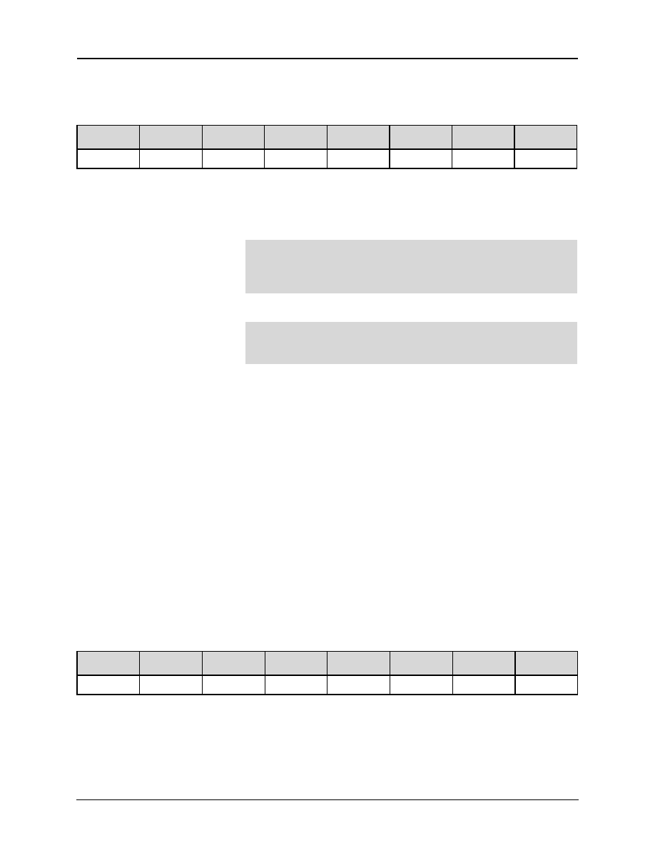
500238B
Mindspeed TechnologiesTM
8
-
77
Advance Information
CX29503 Data Sheet
Register Description
WORD0: Message Status
EOM[1, 0]
End Of Message (EOM)--Receive data link reports an EOM status for each occurrence of a
complete (Good), a continued (Partial), an errored (FCS/Non-integer), or an aborted (Abort)
message.
If an abort or error status with a 0 byte count is reported after the processor has already
buffered a prior HDLC Partial message, that partial buffered processor data should be
discarded. Abort status is reported if the receiver detects a string of 7 or more consecutive 1s
during an HDLC message. FCS error status is reported if the FCS mode is enabled, and the
checksum calculated over the received HDLC message does not match the received 16-bit
FCS. Non-integer error status is reported if the receiver detects a closing Flag character that
yields an HDLC message length which is not an integer number of 8-bit octets.
00 = Good
01 = FCS/Non-integer
10 = Abort
11 = Partial
RDL1_CNT[5:0]
Byte Count [5:0]--Indicates the number of Message Data [WORD1] bytes that are stored in
subsequent consecutive FIFO locations, constituting one received message. The reported byte
count is the actual number of bytes, in the range of 0≠63 bytes, where 0 indicates 0 bytes for
the processor to read. The processor can either read the specified number of message data
bytes consecutively from RDL1 or can poll RDL1_STAT after reading each data byte until
RDL1_STAT reports an EOM (i.e., RMPTY1 = 1 or RSTAT1 = 1).
WORD1: Message Data
RDL1[7:0]
Receive Message Data--Filled by the receiver data link, from LSB to MSB, with bits from the
selected channel. The processor reads 8-bit FIFO data during HDLC and Pack8 modes. During
Pack6 mode, only the 6 LSBs RDL1[5:0] are filled.
7
6
5
4
3
2
1
0
EOM[1]
EOM[0]
RDL1_CNT[5]
RDL1_CNT[4] RDL1_CNT[3]
RDL1_CNT[2] RDL1_CNT[1]
RDL1_CNT[0]
NOTE:
Properly received unformatted messages are reported with a Partial EOM status. The
processor responds to Good or Partial status by reading the indicated number of data
bytes [RDL1_CNT] from RDL1. For abort or error cases, RDL1_CNT = 0 to indicate
that all received data from that message was discarded.
NOTE:
A Good status with RDL1_CNT = 0 is reported if the processor reads RDL1 while the
receiver is in progress of filling the FIFO (in which case RDL1_STAT contains RSTAT1
= 1 and RMSG1 = 1).
7
6
5
4
3
2
1
0
RDL1[7]
RDL1[6]
RDL1[5]
RDL1[4]
RDL1[3]
RDL1[2]
RDL1[1]
RDL1[0]

8-78
Mindspeed TechnologiesTM
500238B
Advance Information
Register Description
CX29503 Data Sheet
0xA9--RDL 1 Status (RDL1_STAT)
Unused bits are reserved and should be written to 0.
RMSG1
In-Progress Receive Message--Real-time status of the Receive Message sequencer is provided
mostly for processor polled applications. During HDLC modes, RMSG1 is high for the
interval between opening and closing Flag characters to indicate the receiver is actively filling
FIFO locations (in which case RSTAT1 is also held high). RMSG1 is low while the channel
receives Flag or Abort characters. During unformatted modes, RMSG1 is high continuously.
0 = channel idle
1 = channel actively filling FIFO
RSTAT1
Next FIFO Read Equals Message Status--For non-empty FIFO conditions (RMPTY1 = 0),
RSTAT1 indicates that the next byte read from RDL1 returns WORD0 message status or
WORD1 message data.
The processor polls RSTAT1 before reading RDL1 to determine how to interpret the RDL1
read byte value or the processor checks RSTAT1 in response to RMSG interrupt
[ISR2; addr: 009].
0 = RDL1 byte equals Message Data (or empty FIFO, if RMTPY1 = 1)
1 = RDL1 byte equals Message Status (if RMPTY1 = 0)
RMPTY1
Receive FIFO Empty--Indicates no data or status bytes are present in the receive data link
FIFO.
0 = FIFO contains data or status as indicated by RSTAT1
1 = FIFO empty
RNEAR1
Receive FIFO Near Full--Indicates data link has filled receive FIFO to the near-full threshold
level specified in FFC[5:0]. Upon reaching the near-full level, the receiver updates the
message status byte [WORD0] placed on top of the FIFO and reports the current in progress
message with a partial EOM status. The processor must read those filled FIFO locations to
clear the RNEAR1 status indicator and to enable the next RNEAR interrupt.
0 = FIFO depth is below the near-full level
1 = FIFO has been filled to the near-full level
RFULL1
Receive FIFO Full--Indicates the data link has completely filled 64 byte locations in the
receive FIFO. In all cases, RFULL1 is an error, indicating the processor did not keep pace with
the receiver and indicates one or more received messages were discarded after the FIFO
became full. The FIFO may still contain one or more Good received messages, and the
processor may still process all receive FIFO contents as usual. However, any message that was
in progress when FIFO reached full is discarded and is also reported with partial EOM status
and a 0 byte count (which distinguishes a full EOM status from a normal abort or error
message status).
0 = FIFO is less than full
1 = FIFO has been completely filled
7
6
5
4
3
2
1
0
--
--
--
RMSG1
RSTAT1
RMPTY1
RNEAR1
RFULL1
NOTE:
RSTAT1 = 0 if the FIFO is empty and there is no message in progress.

500238B
Mindspeed TechnologiesTM
8
-
79
Advance Information
CX29503 Data Sheet
Register Description
0xAA--Performance Report Message (PRM)
Reserved bits should be written to 0.
AUTO_PRM
Automatic PRM Insertion--AUTO_PRM instructs the data link transmitter to format and send
a PRM on the selected transmit channel after each occurrence of the OneSec interrupt. To
meet PRM requirements specified in ANSI T1.403-1995, FCS mode [DL1_CTL; addr: 0A6]
and One-Second error count latching [LATCH_CNT; addr: 046] must both be enabled. In
addition, the data link channel must be selected to output on Facility Data Link (FDL) framing
bits [DL1_TS = 0x40; addr: 0A4]. Octets 1≠14 of the transmit PRM message contents are
automatically encoded (see
Table 8-36
). The encodings are based on the number of received
CRC, FPS, SEF, and FRED errors [addr: 050≠05A]. The remaining PRM message contents
typically remain fixed and are supplied by the processor from other bits that follow in the PRM
register.
0 = no automatic PRM
1 = send PRM automatically every OneSec
7
6
5
4
3
2
1
0
AUTO_PRM
PRM_CR
PRM_R
PRM_U1
PRM_U2
PRM_SL
RESERVED
SEND_PRM
NOTE:
BOP priority code word transmissions are interrupted by AUTO_PRM if TDL1 is
granted output priority [TBOP_MODE = 11; addr: 0A0].
NOTE:
The AUTO_PRM messages take up no space in the transmit data link FIFO, but are
inserted on the transmit channel only after the FIFO is empty. Therefore, if the
processor needs to transmit another type of FDL message between PRM messages,
the processor must write that message after AUTO_PRM has begun sending (i.e.,
after OneSec interrupt).

8-80
Mindspeed TechnologiesTM
500238B
Advance Information
Register Description
CX29503 Data Sheet
PRM_CR
Transmit CR Message Bit--The processor writes the selected C/R bit value to send in each
PRM.
PRM_R
Transmit R Message Bit--The processor writes the selected R bit value to send in each PRM.
PRM_U1
Transmit U1 Message Bit--The processor writes the selected U1 bit value to send in each
PRM.
PRM_U2
Transmit U2 Message Bit--The processor writes the selected U2 bit value to send in each
PRM.
PRM_SL
Transmit SL Message Bit--The processor writes the selected SL bit value to send in each
PRM.
SEND_PRM
Immediately Generate and Send PRM--Similar to AUTO_PRM mode, SEND_PRM instructs
the data link transmitter to format and send a PRM according to ANSI T1.403-1995. But
SEND_PRM executes immediately rather than waiting for the OneSec interrupt. Thus
SEND_PRM gives processor control over PRM transmit timing. This is easier for the
processor to manage if other FDL message types must also be transmitted.
Table 8-36. Performance Report Message (PRM) Structure
Octet No.
LSB
MSB
1
FLAG
2
SAPI
C/R
EA
3
TEI
EA
4
CONTROL
5
G3
LV
G4
U1
U2
G5
SL
G6
6
FE
SE
LB
G1
R
G2
Nm
NI
7
G3
LV
G4
U1
U2
G5
SL
G6
8
FE
SE
LB
G1
R
G2
Nm
NI
9
G3
LV
G4
U1
U2
G5
SL
G6
10
FE
SE
LB
G1
R
G2
Nm
NI
11
G3
LV
G4
U1
U2
G5
SL
G6
12
FE
SE
LB
G1
R
G2
Nm
NI
13
FCS (MSB)
14
FCS (LSB)
GENERAL NOTE:
1. The 1-second report consists of octets 5≠12.
2. R, U1, and U2 are reserved for future standardization and should be set to 0.

500238B
Mindspeed TechnologiesTM
8
-
81
Advance Information
CX29503 Data Sheet
Register Description
0xAB--TDL 1 FIFO Empty Control (TDL1_FEC)
Unused bits are reserved and should be written to 0.
FEC[5:0]
Near-Empty Transmit FIFO Threshold--Selects the FIFO depth of the near-empty interrupt
[TNEAR; addr: 009] and near-empty level status [TNEAR1; addr: 0AE]. The TNEAR
interrupt is activated when the number of data bytes remaining to be transmitted from the FIFO
falls below the selected threshold, see
Table 8-37
. The TNEAR1 indicator is active as long as
the number of processor-filled FIFO locations is below the selected threshold. TNEAR1 is
active-high when the transmit FIFO is completely empty and remains active until the processor
writes the selected threshold number of bytes to TDL1 [addr: 0AD].
Assuming the processor writes 64 bytes to completely fill an empty FIFO, then a TNEAR
interrupt occurs after the transmitter has sent the number of bytes required to bring the FIFO
level back down below the selected threshold. Hence, the processor can consecutively write
64≠FEC[5:0] number of bytes to the transmit FIFO in response to a TNEAR interrupt. The
interrupt also signifies how much time remains (in bytes) for the processor to write TDL1
before the transmit FIFO is emptied. Typically, FEC[5:0] is set to a small value (below the 10-
byte threshold) to minimize the number of TNEAR interrupts and maximize the time between
TNEAR interrupts.
7
6
5
4
3
2
1
0
--
--
FEC[5]
FEC[4]
FEC[3]
FEC[2]
FEC[1]
FEC[0]
Table 8-37. TNEAR Interrupt Threshold
FEC[5:0]
Byte threshold at TNEAR
Empty at TNEAR
00 0000
Disabled
Disabled
00 0001
1 byte threshold
63 empty
00 0010
2 byte threshold
62 empty
.
.
.
.
.
.
.
.
.
--
--
--
11 1110
62 byte threshold
2 empty
11 1111
63 byte threshold
1 empty

8-82
Mindspeed TechnologiesTM
500238B
Advance Information
Register Description
CX29503 Data Sheet
0xAC--TDL 1 End Of Message Control (TDL1_EOM)
Unused bits are reserved and should be written to 0.
TDL1_EOM
End-of-Transmit Message. Writing any data value to TDL1_EOM marks the last byte of data
written into the transmit FIFO as the end of an HDLC message (FCS or Non-FCS mode) or
marks the end of a transmit circular buffer. The processor must write TDL1_EOM after
writing a complete message or the last byte of a circular buffer into TDL1 [addr: 0AD]. The
written data value is ignored and cannot be read back. Multiple HDLC messages are allowed to
be queued in the transmit FIFO simultaneously. In addition, the transition from one circular
buffer to another occurs only after the EOM byte of the current circular buffer has been sent.
0AD--Transmit Data Link FIFO 1 (TDL1)
TDL1[7:0]
Transmit Message Data--Output by the transmitter data link, from LSB to MSB, and sent on
the selected time slot bits. The processor writes 8-bit FIFO data during HDLC and Pack8
modes. During Pack6 mode, only the 6 LSBits TDL1[5:0] are used.
7
6
5
4
3
2
1
0
--
--
--
--
--
--
--
--
7
6
5
4
3
2
1
0
TDL1[7]
TDL1[6]
TDL1[5]
TDL1[4]
TDL1[3]
TDL1[2]
TDL1[1]
TDL1[0]

500238B
Mindspeed TechnologiesTM
8
-
83
Advance Information
CX29503 Data Sheet
Register Description
0xAE--TDL 1 Status (TDL1_STAT)
Unused bits are reserved and should be written to 0.
TMSG1
In-Progress Transmit Message--The real-time status of the transmit message sequencer is
provided mostly for diagnostic purposes. During HDLC modes, TMSG1 is high for the
interval between opening and closing Flag characters. This indicates that the transmitter is
actively pulling data bytes from transmit FIFO locations. TMSG1 is low while the channel
transmits Flag or Abort characters. During unformatted and circular buffer modes, TMSG1 is
high continuously.
0 = channel idle
1 = channel actively emptying FIFO
TMPTY1
Transmit FIFO Empty--Indicates no message data is present in the transmit data link FIFO.
This is typically checked by the processor in response to a TMSG or TNEAR interrupt. If this
is a TMSG interrupt, the processor checks TMPTY1 to determine that all queued messages
were sent (TMPTY1 = 1) or more queued messages remain to be sent (TMPTY1 = 0). If this is
a TNEAR interrupt, the processor confirms TMPTY1 = 0 to verify the partial transmit
message was not aborted by a FIFO underrun.
0 = FIFO contains data to be transmitted
1 = FIFO empty
TNEAR1
Transmit FIFO-Near Empty--Indicates the data link has emptied the transmit FIFO to below
the near-empty threshold specified in FEC[5:0]. After sending the byte that occupied the near-
empty FIFO threshold level, TNEAR1 goes active-high, which generates a TNEAR interrupt.
The processor must write data to TDL1 to fill the transmit FIFO beyond the near-empty
threshold to clear TNEAR1 status and enable the next TNEAR interrupt event.
0 = FIFO depth is below the near-empty level
1 = FIFO has been emptied past the near-empty level
TFULL1
Transmit FIFO Full--Indicates the processor has completely filled 64 byte locations in the
transmit FIFO. While TFULL1 remains active, any subsequent processor writes to TDL1 are
ignored. If the processor should inadvertently write to TDL1 while TFULL1 is active, the
processor must allow FIFO to become completely empty without writing to TDL1_EOM to
force the transmitter to send an Abort character.
0 = FIFO is less than full
1 = FIFO has been completely filled
7
6
5
4
3
2
1
0
--
--
--
--
TMSG1
TMPTY1
TNEAR1
TFULL1

8-84
Mindspeed TechnologiesTM
500238B
Advance Information
Register Description
CX29503 Data Sheet
8.3.2.12
Data Link Test Registers
0xBA--DLINK Test Configuration (DL_TEST1)
Data link test registers [addr: 0BA≠0BE] are for Mindspeed production test. Set to 0 for normal operation.
Unused bits are reserved and should be written to 0.
DL_TEST1[3]
Clock Test--Zero for normal operation, where clocks controlled by DL1_CTL and DL2_CTL
[addr: 0A6, 0B1]. When active-high, clocks are always enabled.
DL_TEST1[2]
Shadow Select--Report shadow pointers instead of normal read/write pointers.
DL_TEST1[1, 0]
FIFO Select: 00 = RDL1; 10 = TDL1; 01 and 11 = not applicable.
0xBB--DLINK Test Status (DL_TEST2)
Unused bits are reserved and should be written to 0.
DL_TEST2[5:0]
Read or Shadow Read Pointer--Reports selected FIFO read pointer current address.
0xBC--DLINK Test Status (DL_TEST3)
Unused bits are reserved and should be written to 0.
DL_TEST3[5:0]
Write or Shadow Write Pointer--Specifies selected FIFO write pointer address.
0xBD--DLINK Test Control 1 or Configuration 1 (DL_TEST4)
DL_TEST4[6]
TFIFO1 Read Clear--Force transmit FIFO read pointer to empty
DL_TEST4[5]
TFIFO1 Write Clear--Force transmit FIFO write pointer to empty
DL_TEST4[4]
TFIFO1 Write--MPU data goes to specified write pointer address
DL_TEST4[3]
RFIFO1 Read Clear--Force receive FIFO read pointer to empty state (flush)
DL_TEST4[2]
RFIFO1 Write Clear--Force receive FIFO write pointer to empty state (flush)
DL_TEST4[1]
RFIFO1 Write--MPU data goes to specified write pointer address
DL_TEST4[0]
RFIFO1 Bypass--Pipe receive data
7
6
5
4
3
2
1
0
--
--
--
--
DL_TEST1[3]
DL_TEST1[2]
DL_TEST1[1]
DL_TEST1[0]
7
6
5
4
3
2
1
0
--
--
DL_TEST2[5]
DL_TEST2[4]
DL_TEST2[3]
DL_TEST2[2]
DL_TEST2[1]
DL_TEST2[0]
7
6
5
4
3
2
1
0
--
--
DL_TEST3[5]
DL_TEST3[4]
DL_TEST3[3]
DL_TEST3[2]
DL_TEST3[1]
DL_TEST3[0]
7
6
5
4
3
2
1
0
--
DL_TEST4[6]
DL_TEST4[5]
DL_TEST4[4]
DL_TEST4[3]
DL_TEST4[2]
DL_TEST4[1]
DL_TEST4[0]

500238B
Mindspeed TechnologiesTM
8
-
85
Advance Information
CX29503 Data Sheet
Register Description
8.3.2.13
Payload Loopback Status Register
0xD9--Payload Loopback Status Register (PLB_STAT)
Plb_overflow_underflow
This bit indicates that the payload loopback FIFO in the DS1/E1 framer has overflowed or
underflowed. This bit is cleared on read.
0 = Indicates that no overflow has occurred
1 = Indicates that an overflow condition has occurred
7
6
5
4
3
2
1
0
--
--
--
--
--
--
Plb_overflow_
underflow
--

8-86
Mindspeed TechnologiesTM
500238B
Advance Information
Register Description
CX29503 Data Sheet
8.4
M13/E13 Multiplexer/Demultiplexer (MUX/DEMUX)
This section describes all registers within each M13/E13 block including the DS3/E3 framer block, and seven
DS2/E2 framers. There are three M13/E13 blocks within the CX29503. The address of each register is the offset
from the start of the applicable MUX/DEMUX block.
Table 8-38. M13/E13 MUX/DEMUX Block Register Map <tableContinuation>(1 of 3)
M13/E13 Global Control and Status Registers (
Section 8.4.1
)
Offset
(Hex)
Type
Register Description
Clear on
Read
Value After Reset
(Hex or Undefined)
5000
R/W
M13/E13 System Control Register
No
0x00
5001≠
5005
--
Undefined
--
--
5006
R/W
DS3/E3 Framer Control Register
No
0x00
5007
R
M13 Interrupt Source Status Register
No
0x00
5008
--
Undefined
--
--
5009
R/W
DS2/E2 Channel 1 Framer Control Register
No
0x00
500A
R/W
DS2/E2 Channel 2 Framer Control Register
No
0x00
500B
R/W
DS2/E2 Channel 3 Framer Control Register
No
0x00
500C
R/W
DS2/E2 Channel 4 Framer Control Register
No
0x00
500D
R/W
DS2/E2 Channel 5 Framer Control Register
No
0x00
500E
R/W
DS2/E2 Channel 6 Framer Control Register
No
0x00
500F
R/W
DS2/E2 Channel 7 Framer Control Register
No
0x00
5010
R/W
DS2/E2 Channel 1 Loopback Control Register (type 2)
No
0x00
5011
R/W
DS2/E2 Channel 2 Loopback Control Register (type 2)
No
0x00
5012
R/W
DS2/E2 Channel 3 Loopback Control Register (type 2)
No
0x00
5013
R/W
DS2/E2 Channel 4 Loopback Control Register (type 2)
No
0x00
5014
R/W
DS2/E2 Channel 5 Loopback Control Register (type 2)
No
0x00
5015
R/W
DS2/E2 Channel 6 Loopback Control Register (type 2)
No
0x00
5016
R/W
DS2/E2 Channel 7 Loopback Control Register (type 2)
No
0x00
5017
R/W
M13/E13 Group 1 (Channels 1≠8) Interrupt Enable
No
0x00
5018
R/W
M13/E13 Group 2 (Channels 9≠16) Interrupt Enable
No
0x00
5019
R/W
M13/E13 Group 3 (Channels 17≠24) Interrupt Enable
No
0x00
501A
R/W
M13/E13 Group 4 (Channels 25≠28) Interrupt Enable
No
0x00
501B
R/W
M13/E13 Channel 1 Control Register
No
0x00
501C
R/W
M13/E13 Channel 2 Control Register
No
0x00
501D
R/W
M13/E13 Channel 3 Control Register
No
0x00
501E
R/W
M13/E13 Channel 4 Control Register
No
0x00
501F
R/W
M13/E13 Channel 5 Control Register
No
0x00

500238B
Mindspeed TechnologiesTM
8
-
87
Advance Information
CX29503 Data Sheet
Register Description
5020
R/W
M13/E13 Channel 6 Control Register
No
0x00
5021
R/W
M13/E13 Channel 7 Control Register
No
0x00
5022
R/W
M13/E13 Channel 8 Control Register
No
0x00
5023
R/W
M13/E13 Channel 9 Control Register
No
0x00
5024
R/W
M13/E13 Channel 10 Control Register
No
0x00
5025
R/W
M13/E13 Channel 11 Control Register
No
0x00
5026
R/W
M13/E13 Channel 12 Control Register
No
0x00
5027
R/W
M13/E13 Channel 13 Control Register
No
0x00
5028
R/W
M13/E13 Channel 14 Control Register
No
0x00
5029
R/W
M13/E13 Channel 15 Control Register
No
0x00
502A
R/W
M13/E13 Channel 16 Control Register
No
0x00
502B
R/W
M13/E13 Channel 17 Control Register
No
0x00
502C
R/W
M13/E13 Channel 18 Control Register
No
0x00
502D
R/W
M13/E13 Channel 19 Control Register
No
0x00
502E
R/W
M13/E13 Channel 20 Control Register
No
0x00
502F
R/W
M13/E13 Channel 21 Control Register
No
0x00
5030
R/W
M13/E13 Channel 22 Control Register
No
0x00
5031
R/W
M13/E13 Channel 23 Control Register
No
0x00
5032
R/W
M13/E13 Channel 24 Control Register
No
0x00
5033
R/W
M13/E13 Channel 25 Control Register
No
0x00
5034
R/W
M13/E13 Channel 26 Control Register
No
0x00
5035
R/W
M13/E13 Channel 27 Control Register
No
0x00
5036
R/W
M13/E13 Channel 28 Control Register
No
0x00
5037
R/W
M13/E13 Channel 1 Line Loopback Control Register (type 4)
No
0x00
5038
R/W
M13/E13 Channel 2 Line Loopback Control Register (type 4)
No
0x00
5039
R/W
M13/E13 Channel 3 Line Loopback Control Register (type 4)
No
0x00
503A
R/W
M13/E13 Channel 4 Line Loopback Control Register (type 4)
No
0x00
503B
R/W
M13/E13 Channel 5 Line Loopback Control Register (type 4)
No
0x00
503C
R/W
M13/E13 Channel 6 Line Loopback Control Register (type 4)
No
0x00
503D
R/W
M13/E13 Channel 7 Line Loopback Control Register (type 4)
No
0x00
503E
R/W
M13/E13 Channel 8 Line Loopback Control Register (type 4)
No
0x00
503F
R/W
M13/E13 Channel 9 Line Loopback Control Register (type 4)
No
0x00
5040
R/W
M13/E13 Channel 10 Line Loopback Control Register (type 4)
No
0x00
Table 8-38. M13/E13 MUX/DEMUX Block Register Map <tableContinuation>(2 of 3)
M13/E13 Global Control and Status Registers (
Section 8.4.1
)
Offset
(Hex)
Type
Register Description
Clear on
Read
Value After Reset
(Hex or Undefined)

8-88
Mindspeed TechnologiesTM
500238B
Advance Information
Register Description
CX29503 Data Sheet
5041
R/W
M13/E13 Channel 11 Line Loopback Control Register (type 4)
No
0x00
5042
R/W
M13/E13 Channel 12 Line Loopback Control Register (type 4)
No
0x00
5043
R/W
M13/E13 Channel 13 Line Loopback Control Register (type 4)
No
0x00
5044
R/W
M13/E13 Channel 14 Line Loopback Control Register (type 4)
No
0x00
5045
R/W
M13/E13 Channel 15 Line Loopback Control Register (type 4)
No
0x00
5046
R/W
M13/E13 Channel 16 Line Loopback Control Register (type 4)
No
0x00
5047
R/W
M13/E13 Channel 17 Line Loopback Control Register (type 4)
No
0x00
5048
R/W
M13/E13 Channel 18 Line Loopback Control Register (type 4)
No
0x00
5049
R/W
M13/E13 Channel 19 Line Loopback Control Register (type 4)
No
0x00
504A
R/W
M13/E13 Channel 20 Line Loopback Control Register (type 4)
No
0x00
504B
R/W
M13/E13 Channel 21 Line Loopback Control Register (type 4)
No
0x00
504C
R/W
M13/E13 Channel 22 Line Loopback Control Register (type 4)
No
0x00
504D
R/W
M13/E13 Channel 23 Line Loopback Control Register (type 4)
No
0x00
504E
R/W
M13/E13 Channel 24 Line Loopback Control Register (type 4)
No
0x00
504F
R/W
M13/E13 Channel 25 Line Loopback Control Register (type 4)
No
0x00
5050
R/W
M13/E13 Channel 26 Line Loopback Control Register (type 4)
No
0x00
5051
R/W
M13/E13 Channel 27 Line Loopback Control Register (type 4)
No
0x00
5052
R/W
M13/E13 Channel 28 Line Loopback Control Register (type 4)
No
0x00
5052≠
51FF
--
Undefined
--
--
Table 8-38. M13/E13 MUX/DEMUX Block Register Map <tableContinuation>(3 of 3)
M13/E13 Global Control and Status Registers (
Section 8.4.1
)
Offset
(Hex)
Type
Register Description
Clear on
Read
Value After Reset
(Hex or Undefined)

500238B
Mindspeed TechnologiesTM
8
-
89
Advance Information
CX29503 Data Sheet
Register Description
Table 8-39. DS3/E3 Framer Register Map <tableContinuation>(1 of 3)
DS3/E3 Framer Registers (
Section 8.4.2
)
Offset
(Hex)
Type
Register Description
Clear
on
Read
Value After Reset
(Hex or Undefined)
5200≠
521F
--
Reserved
--
--
5220
R/W
Mode Control Register
No
0x00
5221
R/W
Counter Interrupt Enable Register
No
0x00
5222
R/W
Alarm Start Interrupt Enable Register
No
0x00
5223
R/W
Alarm End Interrupt Enable Register
No
0x00
5224
R/W
Feature 1 Control Register
No
0x07
5225
R/W
Feature 2 Control Register
No
0x01
5226
R/W
Feature 3 Control Register
No
0x00
5227
R/W
Feature 4 Control Register
No
0x00
5228
R/W
Feature 5 Control Register
No
0x00
5229
R/W
Transmit Overhead Insertion 1 Control Register
No
0x00
522A
R/W
Transmit Overhead Insertion 2 Control Register
No
0x00
522B
R/W
REXTCK Control Register
No
0x00
522C
R/W
Receive Overhead Control Register
No
0x00
522D
R/W
Transmit Data Link Control Register
No
0x00
522E
R/W
Transmit Data Link Threshold Control Register
No
0x00
522F
R/W
Transmit Data Link Message LSB
No
--
5230
R/W
Transmit Data Link Message MSB
No
--
5231
R/W
Receive Data Link Control Register
No
0x00
5232
R/W
Receive Data Link Threshold Control Register
No
0x7F
5233
R/W
Transmit FEAC Channel Byte
No
0xFF
5234
--
Reserved
--
--
5235
--
Reserved
--
--
5236≠
523F
--
Undefined
--
--
5240
R
DS3/E3 Maintenance Status Register
No
0x81
5241
R
Interrupt Request Register
No
0x00
5242
R
Counter Interrupt Status Register
No
0x00
5243
R
Alarm Start Interrupt Status Register
Yes
0x00
5244
R
Alarm End Interrupt Status Register
Yes
0x00
5245
--
Reserved
--
--
5246
R
E3-G.832 MA Fields Status Register (not supported)
--
--

8-90
Mindspeed TechnologiesTM
500238B
Advance Information
Register Description
CX29503 Data Sheet
5247
R
E3-G.832 SSM Field Status Register (not supported)
--
--
5248
R
Transmit Data Link and FEAC Interrupt Status Register
Partial
0x03
5249
--
Reserved
--
--
524A
--
Reserved
--
--
524B
R
Receive Data Link Interrupt Status Register
Partial
bits 0, 5 = undefined
bits 1≠4, 6, and 7 = 0
524C
R
Receive Data Link Message Byte
No
--
524D
--
Reserved
--
--
524E
--
Reserved
--
--
524F
R
Receive FEAC Byte
No
--
5250
R
Receive FEAC Stack Byte
No
bits 2≠7 = undefined
bits 0 and 1 = 0
5251
R
Receive FEAC Interrupt Status Register
Partial
0x00
5252
R
Receive AIC Byte
No
--
5253≠
525F
--
Undefined
--
--
5260
R/W
DS3/E3 Parity Error Counter--Low Byte
No
0x00
5261
R/W
DS3/E3 Parity Error Counter--High Byte
No
0x00
5262
R/W
DS3 Parity Disagreement Counter--Low Byte
No
0x00
5263
R/W
DS3 Parity Disagreement Counter--High Byte
No
0x00
5264
R/W
DS3 X-Bit Disagreement Counter--Low Byte
No
0x00
5265
R/W
DS3 X-Bit Disagreement Counter--High Byte
No
0x00
5266
R/W
DS3/E3 Frame Error Counter--Low Byte
No
0x00
5267
R/W
DS3/E3 Frame Error Counter--High Byte
No
0x00
5268
R/W
DS3 Path Parity Error Counter--Low Byte
No
0x00
5269
R/W
DS3 Path Parity Error Counter--High Byte
No
0x00
526A
R/W
DS3/E3 FEBE Event Counter--Low Byte
No
0x00
526B
R/W
DS3/E3 FEBE Event Counter--High Byte
No
0x00
526C
R/W
DS3/E3 Excessive 0s Counter--Low Byte
No
0x00
526D
R/W
DS3/E3 Excessive 0s Counter--High Byte
No
0x00
526E
R/W
DS3/E3 LCV Counter--Low Byte
No
0x00
526F
R/W
DS3/E3 LCV Counter--Middle Byte
No
0x00
5270
R/W
DS3/E3 LCV Counter--High Byte
No
0x00
Table 8-39. DS3/E3 Framer Register Map <tableContinuation>(2 of 3)
DS3/E3 Framer Registers (
Section 8.4.2
)
Offset
(Hex)
Type
Register Description
Clear
on
Read
Value After Reset
(Hex or Undefined)

500238B
Mindspeed TechnologiesTM
8
-
91
Advance Information
CX29503 Data Sheet
Register Description
5271≠
53FF
--
Undefined
--
--
Table 8-39. DS3/E3 Framer Register Map <tableContinuation>(3 of 3)
DS3/E3 Framer Registers (
Section 8.4.2
)
Offset
(Hex)
Type
Register Description
Clear
on
Read
Value After Reset
(Hex or Undefined)
Table 8-40. DS2/E2 Framer/MUX Registers Map <tableContinuation>(1 of 4)
DS2/E2 Framer/MUX Registers (
Section 8.4.3
)
Offset
(Hex)
Type
Register Description
Clear
on
Read
Value After Reset
(Hex or Undefined)
5400
R/W
DS2/E2 Interrupt Enable
No
0x00
5401
R
DS2/E2 Interrupt Status
No
0x00
5402
R
DS2/E3 Framer Status
No
0x7F
5403
R/W
DS2/E2 Framer 1 Transmit Control Register
No
0x00
5404
R/W
DS2/E2 Framer 1 Receive Control Register
No
0x00
5405
R/W
DS2/E2 Framer 1 Counter/Loopback Interrupt Enable
No
0x00
5406
R/W
DS2/E2 Framer 1 Alarm Start Interrupt Enable
No
0x00
5407
R/W
DS2/E2 Framer 1 Alarm End Interrupt Enable
No
0x00
5408
R
DS2/E2 Framer 1 Transmit FIFO Status
No
0x00
5409
R
DS2/E2 Framer 1 Counter/Loopback Interrupt Status
Yes
0x00
540A
R
DS2/E2 Framer 1 Alarm Start Interrupt Status
Yes
0x00
540B
R
DS2/E2 Framer 1 Alarm End Interrupt Status
Yes
0x00
540C
R
DS2/E2 Framer 1 Receive Frame Error Counter
No
0x00
540D
R
DS2/E2 Framer 1 Receive M Bit Error Counter
No
0x00
540E
R
DS2/E2 Framer 1 Receive LOS Counter
No
0x00
540F
R
DS2/E2 Framer 1 Receive Parity Error Counter (Lower Byte)
No
0x00
5410
R
DS2/E2 Framer 1 Receive Parity Error Counter (Upper Byte)
No
0x00
5411
R
DS2/E2 Framer 1 National Use Bit Status
No
0x00
5412≠
541F
--
Unused
--
--
5420≠
5422
--
Reserved
--
--
5423
R
DS2/E2 Framer 2 Transmit Control Register
No
0x00
5424
R
DS2/E2 Framer 2 Receive Control Register
No
0x00
5425
R/W
DS2/E2 Framer 2 Counter/Loopback Interrupt Enable
No
0x00
5426
R/W
DS2/E2 Framer 2 Alarm Start Interrupt Enable
No
0x00
5427
R/W
DS2/E2 Framer 2 Alarm End Interrupt Enable
No
0x00

8-92
Mindspeed TechnologiesTM
500238B
Advance Information
Register Description
CX29503 Data Sheet
5428
R
DS2/E2 Framer 2 Transmit FIFO Status
No
0x00
5429
R
DS2/E2 Framer 2 Counter/Loopback Interrupt Status
Yes
0x00
542A
R
DS2/E2 Framer 2 Alarm Start Interrupt Status
Yes
0x00
542B
R
DS2/E2 Framer 2 Alarm End Interrupt Status
Yes
0x00
542C
R
DS2/E2 Framer 2 Receive Frame Error Counter
No
0x00
542D
R
DS2/E2 Framer 2 Receive M Bit Error Counter
No
0x00
542E
R
DS2/E2 Framer 2 Receive LOS Counter
No
0x00
542F
R
DS2/E2 Framer 2 Receive Parity Error Counter (Lower Byte)
No
0x00
5430
R
DS2/E2 Framer 2 Receive Parity Error Counter (Upper Byte)
No
0x00
5431
R
DS2/E2 Framer 2 National Use Bit Status
No
0x00
5432≠
543F
--
Unused
--
--
5440≠
5442
--
Reserved
--
--
5443
R/W
DS2/E2 Framer 3 Transmit Control Register
No
0x00
5444
R/W
DS2/E2 Framer 3 Receive Control Register
No
0x00
5445
R/W
DS2/E2 Framer 3 Counter/Loopback Interrupt Enable
No
0x00
5446
R/W
DS2/E2 Framer 3 Alarm Start Interrupt Enable
No
0x00
5447
R/W
DS2/E2 Framer 3 Alarm End Interrupt Enable
No
0x00
5448
R
DS2/E2 Framer 3 Transmit FIFO Status
No
0x00
5449
R
DS2/E2 Framer 3 Counter/Loopback Interrupt Status
Yes
0x00
544A
R
DS2/E2 Framer 3 Alarm Start Interrupt Status
Yes
0x00
544B
R
DS2/E2 Framer 3 Alarm End Interrupt Status
Yes
0x00
544C
R
DS2/E2 Framer 3 Receive Frame Error Counter
No
0x00
544D
R
DS2/E2 Framer 3 Receive M Bit Error Counter
No
0x00
544E
R
DS2/E2 Framer 3 Receive LOS Counter
No
0x00
544F
R
DS2/E2 Framer 3 Receive Parity Error Counter (Lower Byte)
No
0x00
5450
R
DS2/E2 Framer 3 Receive Parity Error Counter (Upper Byte)
No
0x00
5451
R
DS2/E2 Framer 3 National Use Bit Status
No
0x00
5452≠
545F
--
Unused
--
--
5460≠
5462
--
Reserved
--
--
5463
R/W
DS2/E2 Framer 4 Transmit Control Register
No
0x00
5464
R/W
DS2/E2 Framer 4 Receive Control Register
No
0x00
5465
R/W
DS2/E2 Framer 4 Counter/Loopback Interrupt Enable
No
0x00
Table 8-40. DS2/E2 Framer/MUX Registers Map <tableContinuation>(2 of 4)
DS2/E2 Framer/MUX Registers (
Section 8.4.3
)
Offset
(Hex)
Type
Register Description
Clear
on
Read
Value After Reset
(Hex or Undefined)

500238B
Mindspeed TechnologiesTM
8
-
93
Advance Information
CX29503 Data Sheet
Register Description
5466
R/W
DS2/E2 Framer 4 Alarm Start Interrupt Enable
No
0x00
5467
R/W
DS2/E2 Framer 4 Alarm End Interrupt Enable
No
0x00
5468
R
DS2/E2 Framer 4 Transmit FIFO Status
No
0x00
5469
R
DS2/E2 Framer 4 Counter/Loopback Interrupt Status
Yes
0x00
546A
R
DS2/E2 Framer 4 Alarm Start Interrupt Status
Yes
0x00
546B
R
DS2/E2 Framer 4 Alarm End Interrupt Status
Yes
0x00
546C
R
DS2/E2 Framer 4 Receive Frame Error Counter
No
0x00
546D
R
DS2/E2 Framer 4 Receive M Bit Error Counter
No
0x00
546E
R
DS2/E2 Framer 4 Receive LOS Counter
No
0x00
546F
R
DS2/E2 Framer 4 Receive Parity Error Counter (Lower Byte)
No
0x00
5470
R
DS2/E2 Framer 4 Receive Parity Error Counter (Upper Byte)
No
0x00
5471
R
DS2/E2 Framer 4 National Use Bit Status
No
--
5472≠
547F
--
Unused
--
--
5480≠
5482
--
Reserved
--
--
5483
R/W
DS2/E2 Framer 5 Transmit Control Register
No
0x00
5484
R/W
DS2/E2 Framer 5 Receive Control Register
No
0x00
5485
R/W
DS2/E2 Framer 5 Counter/Loopback Interrupt Enable
No
0x00
5486
R/W
DS2/E2 Framer 5 Alarm Start Interrupt Enable
No
0x00
5487
R/W
DS2/E2 Framer 5 Alarm End Interrupt Enable
No
0x00
5488
R
DS2/E2 Framer 5 Transmit FIFO Status
No
0x00
5489
R
DS2/E2 Framer 5 Counter/Loopback Interrupt Status
Yes
0x00
548A
R
DS2/E2 Framer 5 Alarm Start Interrupt Status
Yes
0x00
546B
R
DS2/E2 Framer 5 Alarm End Interrupt Status
Yes
0x00
548C
R
DS2/E2 Framer 5 Receive Frame Error Counter
No
0x00
548D
R
DS2/E2 Framer 5 Receive M Bit Error Counter
No
0x00
548E
R
DS2/E2 Framer 5 Receive LOS Counter
No
0x00
548F
R
DS2/E2 Framer 5 Receive Parity Error Counter (Lower Byte)
No
0x00
5490
R
DS2/E2 Framer 5 Receive Parity Error Counter (Upper Byte)
No
0x00
5491≠
549F
--
Unused
--
--
54A0≠
54A2
--
Reserved
--
--
54A3
R/W
DS2/E2 Framer 6 Transmit Control Register
No
0x00
54A4
R/W
DS2/E2 Framer 6 Receive Control Register
No
0x00
Table 8-40. DS2/E2 Framer/MUX Registers Map <tableContinuation>(3 of 4)
DS2/E2 Framer/MUX Registers (
Section 8.4.3
)
Offset
(Hex)
Type
Register Description
Clear
on
Read
Value After Reset
(Hex or Undefined)

8-94
Mindspeed TechnologiesTM
500238B
Advance Information
Register Description
CX29503 Data Sheet
54A5
R/W
DS2/E2 Framer 6 Counter/Loopback Interrupt Enable
No
0x00
54A6
R/W
DS2/E2 Framer 6 Alarm Start Interrupt Enable
No
0x00
54A7
R/W
DS2/E2 Framer 6 Alarm End Interrupt Enable
No
0x00
54A8
R
DS2/E2 Framer 6 Transmit FIFO Status
No
0x00
54A9
R
DS2/E2 Framer 6 Counter/Loopback Interrupt Status
Yes
0x00
54AA
R
DS2/E2 Framer 6 Alarm Start Interrupt Status
Yes
0x00
54AB
R
DS2/E2 Framer 6 Alarm End Interrupt Status
Yes
0x00
54AC
R
DS2/E2 Framer 6 Receive Frame Error Counter
No
0x00
54AD
R
DS2/E2 Framer 6 Receive M Bit Error Counter
No
0x00
54AE
R
DS2/E2 Framer 6 Receive LOS Counter
No
0x00
54AF
R
DS2/E2 Framer 6 Receive Parity Error Counter (Lower Byte)
No
0x00
54B0
R
DS2/E2 Framer 6 Receive Parity Error Counter (Upper Byte)
No
0x00
54B1≠
54BF
--
Unused
--
--
54C0≠
54C2
--
Reserved
--
--
54C3
R/W
DS2/E2 Framer 7 Transmit Control Register
No
0x00
54C4
R/W
DS2/E2 Framer 7 Receive Control Register
No
0x00
54C5
R/W
DS2/E2 Framer 7 Counter/Loopback Interrupt Enable
No
0x00
54C6
R/W
DS2/E2 Framer 7 Alarm Start Interrupt Enable
No
0x00
54C7
R/W
DS2/E2 Framer 7 Alarm End Interrupt Enable
No
0x00
54C8
R
DS2/E2 Framer 7 Transmit FIFO Status
No
0x00
54C9
R
DS2/E2 Framer 7 Counter/Loopback Interrupt Status
Yes
0x00
54CA
R
DS2/E2 Framer 7 Alarm Start Interrupt Status
Yes
0x00
54CB
R
DS2/E2 Framer 7 Alarm End Interrupt Status
Yes
0x00
54CC
R
DS2/E2 Framer 7 Receive Frame Error Counter
No
0x00
54CD
R
DS2/E2 Framer 7 Receive M Bit Error Counter
No
0x00
54CE
R
DS2/E2 Framer 7 Receive LOS Counter
No
0x00
54CF
R
DS2/E2 Framer 7 Receive Parity Error Counter (Lower Byte)
No
0x00
54D0
R
DS2/E2 Framer 7 Receive Parity Error Counter (Upper Byte)
No
0x00
54D1≠
54FF
--
Undefined
No
--
Table 8-40. DS2/E2 Framer/MUX Registers Map <tableContinuation>(4 of 4)
DS2/E2 Framer/MUX Registers (
Section 8.4.3
)
Offset
(Hex)
Type
Register Description
Clear
on
Read
Value After Reset
(Hex or Undefined)

500238B
Mindspeed TechnologiesTM
8
-
95
Advance Information
CX29503 Data Sheet
Register Description
Table 8-41. M13/E13 Control Registers Map <tableContinuation>(1 of 5)
M13/E13 Control Registers (
Section 8.4.4
)
Offset
(Hex)
Type
Register Description
Clear
on
Read
Value After Reset
(Hex or Undefined)
5500
R
M13/E13 Interrupt Status Register 1
No
0x00
5501
R
M13/E13 Interrupt Status Register 2
No
0x00
5502
R
M13/E13 Interrupt Status Register 3
No
0x00
5503
R
M13/E13 Interrupt Status Register 4
No
0x00
5504
--
Undefined
--
--
5505
R/W
M13/E13 Channel 1 Receive Interrupt Enable
No
0x00
5506
R
M13/E13 Channel 1 Transmit FIFO Status
No
0x00
5507
R
M13/E13 Channel 1 Receive Interrupt Status
Yes
0x00
5508≠
550B
--
Reserved
--
--
550C
--
Undefined
--
--
550D
R/W
M13/E13 Channel 2 Receive Interrupt Enable
No
0x00
550E
R
M13/E13 Channel 2 Transmit FIFO Status
No
0x00
550F
R
M13/E13 Channel 2 Receive Interrupt Status
Yes
0x00
5510≠
5513
--
Reserved
--
--
5514
--
Undefined
--
--
5515
R/W
M13/E13 Channel 3 Receive Interrupt Enable
No
0x00
5516
R
M13/E13 Channel 3 Transmit FIFO Status
No
0x00
5517
R
M13/E13 Channel 3 Receive Interrupt Status
Yes
0x00
5518≠
551B
--
Reserved
--
--
551C
--
Undefined
--
--
551D
R/W
M13/E13 Channel 4 Receive Interrupt Enable
No
0x00
551E
R
M13/E13 Channel 4 Transmit FIFO Status
No
0x00
551F
R
M13/E13 Channel 4 Receive Interrupt Status
Yes
0x00
5520≠
5523
--
Reserved
--
--
5524
--
Undefined
--
--
5525
R/W
M13/E13 Channel 5 Receive Interrupt Enable
No
0x00
5526
R
M13/E13 Channel 5 Transmit FIFO Status
No
0x00
5527
R
M13/E13 Channel 5 Receive Interrupt Status
Yes
0x00
5528≠
552B
--
Reserved
--
--

8-96
Mindspeed TechnologiesTM
500238B
Advance Information
Register Description
CX29503 Data Sheet
552C
--
Undefined
--
--
552D
R/W
M13/E13 Channel 6 Receive Interrupt Enable
No
0x00
552E
R
M13/E13Channel 6 Transmit FIFO Status
No
0x00
552F
R
M13/E13 Channel 6 Receive Interrupt Status
Yes
0x00
5530≠
5533
--
Reserved
--
--
5534
--
Undefined
--
--
5535
R/W
M13/E13 Channel 7 Receive Interrupt Enable
No
0x00
5536
R
M13/E13 Channel 7 Transmit FIFO Status
No
0x00
5537
R
M13/E13 Channel 7 Receive Interrupt Status
Yes
0x00
5538≠
553B
--
Reserved
--
--
553C
--
Undefined
--
--
553D
R/W
M13/E13 Channel 8 Receive Interrupt Enable
No
0x00
553E
R
M13/E13 Channel 8 Transmit FIFO Status
No
0x00
553F
R
M13/E13 Channel 8 Receive Interrupt Status
Yes
0x00
5540≠
5543
--
Reserved
--
--
5544
--
Undefined
--
--
5545
R/W
M13/E13 Channel 9 Receive Interrupt Enable
No
0x00
5546
R
M13/E13 Channel 9 Transmit FIFO Status
No
0x00
5547
R
M13/E13 Channel 9 Receive Interrupt Status
Yes
0x00
5548≠
554B
--
Reserved
--
--
554C
--
Undefined
--
--
554D
R/W
M13/E13 Channel 10 Receive Interrupt Enable
No
0x00
554E
R
M13/E13 Channel 10 Transmit FIFO Status
No
0x00
554F
R
M13/E13 Channel 10 Receive Interrupt Status
Yes
0x00
5550≠
5553
--
Reserved
--
--
5554
--
Undefined
--
--
5555
R/W
M13/E13 Channel 11 Receive Interrupt Enable
No
0x00
5556
R
M13/E13 Channel 11 Transmit FIFO Status
No
0x00
5557
R
M13/E13 Channel 11 Receive Interrupt Status
Yes
0x00
Table 8-41. M13/E13 Control Registers Map <tableContinuation>(2 of 5)
M13/E13 Control Registers (
Section 8.4.4
)
Offset
(Hex)
Type
Register Description
Clear
on
Read
Value After Reset
(Hex or Undefined)

500238B
Mindspeed TechnologiesTM
8
-
97
Advance Information
CX29503 Data Sheet
Register Description
5558≠
555B
--
Reserved
--
--
555C
--
Undefined
--
--
555D
R/W
M13/E13 Channel 12 Receive Interrupt Enable
No
0x00
555E
R
M13/E13 Channel 12 Transmit FIFO Status
No
0x00
555F
R
M13/E13 Channel 12 Receive Interrupt Status
Yes
0x00
5560≠
5563
--
Reserved
--
--
5564
--
Undefined
--
--
5565
R/W
M13/E13Channel 13 Receive Interrupt Enable
No
0x00
5566
R
M13/E13 Channel 13 Transmit FIFO Status
No
0x00
5567
R
M13/E13 Channel 13 Receive Interrupt Status
Yes
0x00
5568≠
556B
--
Reserved
--
--
556C
--
Undefined
--
--
556D
R/W
M13/E13 Channel 14 Receive Interrupt Enable
No
0x00
556E
R
M13/E13 Channel 14 Transmit FIFO Status
No
0x00
556F
R
M13/E13 Channel 14 Receive Interrupt Status
Yes
0x00
5570≠
5573
--
Reserved
--
--
5574
--
Undefined
--
--
5575
R/W
M13/E13 Channel 15 Receive Interrupt Enable
No
0x00
5576
R
M13/E13 Channel 15 Transmit FIFO Status
No
0x00
5577
R
M13/E13 Channel 15 Receive Interrupt Status
Yes
0x00
5578≠
557B
--
Reserved
--
--
557C
--
Undefined
--
--
557D
R/W
M13/E13 Channel 16 Receive Interrupt Enable
No
0x00
557E
R
M13/E13 Channel 16 Transmit FIFO Status
No
0x00
5557F
R
M13/E13 Channel 16 Receive Interrupt Status
Yes
0x00
5580≠
5583
--
Reserved
--
--
5584
--
Undefined
--
--
5585
R/W
M13/E13 Channel 17 Receive Interrupt Enable
No
0x00
5586
R
M13/E13 Channel 17 Transmit FIFO Status
No
0x00
Table 8-41. M13/E13 Control Registers Map <tableContinuation>(3 of 5)
M13/E13 Control Registers (
Section 8.4.4
)
Offset
(Hex)
Type
Register Description
Clear
on
Read
Value After Reset
(Hex or Undefined)

8-98
Mindspeed TechnologiesTM
500238B
Advance Information
Register Description
CX29503 Data Sheet
5587
R
M13/E13 Channel 17 Receive Interrupt Status
Yes
0x00
5588≠
558B
--
Reserved
--
--
558C
--
Undefined
--
--
558D
R/W
M13/E13 Channel 18 Receive Interrupt Enable
No
0x00
558E
R
M13/E13 Channel 18 Transmit FIFO Status
No
0x00
558F
R
M13/E13 Channel 18 Receive Interrupt Status
Yes
0x00
5590≠
5593
--
Reserved
--
--
5594
--
Undefined
--
--
5595
R/W
M13/E13 Channel 19 Receive Interrupt Enable
No
0x00
5596
R
M13/E13 Channel 19 Transmit FIFO Status
No
0x00
5597
R
M13/E13 Channel 19 Receive Interrupt Status
Yes
0x00
5598≠
559B
--
Reserved
--
--
559C
--
Undefined
--
--
559D
R/W
M13/E13 Channel 20 Receive Interrupt Enable
No
0x00
559E
R
M13/E13 Channel 20 Transmit FIFO Status
No
0x00
559F
R
M13/E13 Channel 20 Receive Interrupt Status
Yes
0x00
55A0≠
55A3
--
Reserved
--
--
55A4
--
Undefined
--
--
55A5
R/W
M13/E13 Channel 21 Receive Interrupt Enable
No
0x00
55A6
R
M13/E13 Channel 21 Transmit FIFO Status
No
0x00
55A7
R
M13/E13 Channel 21 Receive Interrupt Status
Yes
0x00
55A8≠
55AB
--
Reserved
--
--
55AC
--
Undefined
--
--
55AD
R/W
M13/E13 Channel 22 Receive Interrupt Enable
No
0x00
55AE
R
M13/E13 Channel 22 Transmit FIFO Status
No
0x00
55AF
R
M13/E13 Channel 22 Receive Interrupt Status
Yes
0x00
55B0≠
55B3
--
Reserved
--
--
55B4
--
Undefined
--
--
55B5
R/W
M13/E13 Channel 23 Receive Interrupt Enable
No
0x00
Table 8-41. M13/E13 Control Registers Map <tableContinuation>(4 of 5)
M13/E13 Control Registers (
Section 8.4.4
)
Offset
(Hex)
Type
Register Description
Clear
on
Read
Value After Reset
(Hex or Undefined)

500238B
Mindspeed TechnologiesTM
8
-
99
Advance Information
CX29503 Data Sheet
Register Description
55B6
R
M13/E13 Channel 23 Transmit FIFO Status
No
0x00
55B7
R
M13/E13 Channel 23 Receive Interrupt Status
Yes
0x00
55B8≠
55BB
--
Reserved
--
--
55BC
--
Undefined
--
--
55BD
R/W
M13/E13 Channel 24 Receive Interrupt Enable
No
0x00
55BE
R
M13/E13 Channel 24 Transmit FIFO Status
No
0x00
55BF
R
M13/E13 Channel 24 Receive Interrupt Status
Yes
0x00
55C0≠
55C3
--
Reserved
--
--
55C4
--
Undefined
--
--
55C5
R/W
M13/E13 Channel 25 Receive Interrupt Enable
No
0x00
55C6
R
M13/E13 Channel 25 Transmit FIFO Status
No
0x00
55C7
R
M13/E13 Channel 25 Receive Interrupt Status
Yes
0x00
55C8≠
55CB
--
Reserved
--
--
55CC
--
Undefined
--
--
55CD
R/W
M13/E13 Channel 26 Receive Interrupt Enable
No
0x00
55CE
R
M13/E13 Channel 26 Transmit FIFO Status
No
0x00
55CF
R
M13/E13 Channel 26 Receive Interrupt Status
Yes
0x00
55D0≠
55D3
--
Reserved
--
--
55D4
--
Undefined
--
--
55D5
R/W
M13/E13 Channel 27 Receive Interrupt Enable
No
0x00
55D6
R
M13/E13 Channel 27 Transmit FIFO Status
No
0x00
55D7
R
M13/E13 Channel 27 Receive Interrupt Status
Yes
0x00
55D8≠
55DB
--
Reserved
--
--
55DC
--
Undefined
--
--
55DD
R/W
M13/E13 Channel 28 Receive Interrupt Enable
No
0x00
55DE
R
M13/E13 Channel 28 Transmit FIFO Status
No
0x00
55DF
R
M13/E13 Channel 28 Receive Interrupt Status
Yes
0x00
55E0≠
55FF
--
Undefined
--
--
Table 8-41. M13/E13 Control Registers Map <tableContinuation>(5 of 5)
M13/E13 Control Registers (
Section 8.4.4
)
Offset
(Hex)
Type
Register Description
Clear
on
Read
Value After Reset
(Hex or Undefined)

8-100
Mindspeed TechnologiesTM
500238B
Advance Information
Register Description
CX29503 Data Sheet
8.4.1
M13/E13 Global Status and Control Registers
0x5000--M13/E13 System Control Register
Reset State
0x00
OneSecMode
One-Second Latching Mode.
M13 Mode
Set to operate M13 in Unchannelized mode; clear to operate M13 in Channelized mode (see
Figure 2-2
).
upl3txclksel[1:0]
Specifies the transmit clock sent to the DS3/E3 Framer (see
Figure 4-1
).
∑ 0x0--selects the receive line clock from either the external RLINECLK or the
SONET module depending on the value of the CK_SRC[1:0] pins. If CK_SRC[1:0] =
0x0 or 0x1, then the SONET module clock is used. If CK_SRC[1:0] = 0x2, or 0x3,
then the external RLINKECLK is used.
∑ 0x1--selects the external CLK_DS3 or CLK_E3 clock depending on the value of the
TXE3_CLK in the Clock Configuration register in the Clock and Test block. If
TXE3_CLK = 0x1, then CLK_E3 is used, otherwise, CLK_DS3 is used.
∑ 0x2 or 0x3--selects the external dejittered Receive Line clock (RXCKI).
0x5006--DS3/E3 Framer Control Register
Reset State
0x00
FrEnable
DS3/E3 framer enabled when set to 1
7
6
5
4
3
2
1
0
--
M13 Mode
--
--
upl3txclksel[1]
upl3txclksel[0]
OneSecMode
--
NOTE:
The value of this register in conjunction with the value on the 1-second interrupt
enable input controls the mode of the DS3/E3 Framer and DS2/E2 Framer
performance monitoring counters, i.e., saturating or rollover. This bit replaces
CX28342/3/4/6/8 DS3/E3 Framer GCR01 Bit 1.
7
6
5
4
3
2
1
0
FrEnable
--
--
--
--
--
--
--
NOTE:
Bit 7 replaces the CX28342/3/4/6/8 DS3 Framer GCR00 Bit 7.

500238B
Mindspeed TechnologiesTM
8
-
101
Advance Information
CX29503 Data Sheet
Register Description
0x5007--M13 Interrupt Source Status Register
The M13 MUX/DEMUX Interrupt Structure is shown in
Figure 8-2
.
Reset State
0x00
M13/E13Ch25-28 Int
Interrupt from M13/E13 Group 4 Stage = Channel 25
≠
28 when set to 1
M13/E13Ch17-24 Int
Interrupt from M13/E13 Group 4 Stage = Channel 17
≠
24 when set to 1
M13/E13Ch9-16 Int
Interrupt from M13/E13 Group 4 Stage = Channel 9
≠
16 when set to 1
M13/E13Ch1-8 Int
Interrupt from M13/E13 Group 4 Stage = Channel 1
≠
8 when set to 1
DS2/E2 Int
Interrupt from DS2/E2 Stage when set to 1
Figure 8-3
shows the Level 3 to Level 1 multiplexing. Note that the M13 channel
numbers are numbered differently than the DS1/E1 framer numbers. A cross-
reference is provided in
Table 8-42
.
7
6
5
4
3
2
1
0
--
--
DS2/E2 Int
M13/E13
Ch1≠8 Int
M13/E13
Ch9≠
16 Int
M13/E13
Ch17≠
24 Int
M13/E13
Ch25≠
28 Int
--

8-102
Mindspeed TechnologiesTM
500238B
Advance Information
Register Description
CX29503 Data Sheet
Figure 8-2. M13 MUX/DEMUX Interrupt Structure
"OR"
M13/E13 Group 1
Interrupt Enable
[addr: 0x5017]
"OR"
M13/E13/E13 MUX/DEMUX Interrupt
(see Figure 3-1)
M13/E13 #1 to #8
Interrupt Status
M13/E13 Interrupt
Source Status
[addr: 5007]
Lpbk_IS
Lpbk_IE
M13/E13 MUX
Channel 1
Receive Interrupt
Enable [addr: 5505]
:
M13/E13 MUX
Channel 8
Receive Interrupt
Enable [addr: 553D]
M13/E13 #9 to #16
Interrupt Status
M13/E13 #17 to #24
Interrupt Status
M13/E13 #25 to #28
Interrupt Status
DS2/E2
Interrupt Status
1 to 8
. .
. .
Lpbk_IS
Lpbk_IE
M13/E13 MUX Channel 1 Receive
Interrupt Status [addr: 5507]
:
M13/E13 MUX Channel 8 Receive
Interrupt Status [addr: 553F]
9 to 16
. . .
"OR"
M13/E13 Group 2
Interrupt Enable
[addr: 0x5018]
. . . .
. . . .
"OR"
M13/E13 Group 3
Interrupt Enable
[addr: 0x5019]
"OR"
M13/E13 Group 4
Interrupt Enable
[addr: 0x501A]
. . . .
. . . .
17 to 24
. . . .
Lpbk_IS
Lpbk_IE
M13/E13 MUX
Channel 9
Receive Interrupt
Enable [addr: 5545]
:
M13/E13 MUX
Channel 16
Receive Interrupt
Enable [addr: 557D]
. .
Lpbk_IS
Lpbk_IE
M13/E13 MUX Channel 9 Receive
Interrupt Status [addr: 5547]
:
M13/E13 MUX Channel 16 Receive
Interrupt Status [addr: 557F]
Lpbk_IS
Lpbk_IE
M13/E13 MUX
Channel 17
Receive Interrupt
Enable [addr: 5585]
:
M13/E13 MUX
Channel 24
Receive Interrupt
Enable [addr: 55BD]
. .
. .
Lpbk_IS
Lpbk_IE
M13/E13 MUX Channel 17 Receive
Interrupt Status [addr: 5587]
:
M13/E13 MUX Channel 24 Receive
Interrupt Status [addr: 55BF]
Lpbk_IS
Lpbk_IE
M13/E13 MUX
Channel 25
Receive Interrupt
Enable [addr: 55C5]
:
M13/E13 MUX
Channel 28
Receive Interrupt
Enable [addr: 55DD]
. .
Lpbk_IS
Lpbk_IE
M13/E13 MUX Channel 25 Receive
Interrupt Status [addr: 55C7]
:
M13/E13 MUX Channel 28 Receive
Interrupt Status [addr: 55DF]
25 to 28
. . . .
. . .
. .
. .

500238B
Mindspeed TechnologiesTM
8
-
103
Advance Information
CX29503 Data Sheet
Register Description
Figure 8-3. M29503 Level 3 to Level 1 Multiplexing
28
T1.107,
or G.742
G.747,
DS2/E2 Framer
& M12/E12 MUX
T1.107,
or G.742
G.747,
T1.107,
or G.742
G.747,
T1.107,
or G.742
G.747,
T1.107,
or G.747
T1.107,
or G.747
T1.107,
or G.747
DS2/E2
DS2/E2
DS2/E2
DS2/E2
DS2
DS2
DS2
4 DS1s,
3/4 E1s
L3
->
L2 D
e
mux
4 DS1s,
3/4 E1s
4 DS1s,
3/4 E1s
4 DS1s,
3/4 E1s
4 DS1s,
3E1s
4 DS1s,
3E1s
4 DS1s,
3E1s
DS1/E1 Framers
(7 instances)
DS1/E1 Framers
(7 instances)
DS1/E1 Framers
(7 instances)
DS1/E1 Framers
(7 instances)
FR1
FR1
FR1
FR1
22
26
18 14
6
10
2
21
25
17 13
5
9
1
23
27
19 15
7
11
3
24 20 16
8
12
4
5
6
4 3
1
2
25
12
13
11 10
8
9
7
19
20
18 17
15
16
14
27
28
26
24
22
23
21
1
2
3
4
5
6
7
8
9
10
11
12
16
13
14
15
20
17
18
19
21
22
23
26
27
28
T1.107: 28 DS1 channels
G.747: 21 E1 channels
G.742: 16 E1 channels
DS1/E1 Framer Number
24
M13 Channel Number
DS2/E2 Framer
& M12/E12 MUX
DS2/E2 Framer
& M12/E12 MUX
DS2/E2 Framer
& M12/E12 MUX
DS2/E2 Framer
& M12/E12 MUX
DS2/E2 Framer
& M12/E12 MUX
DS2/E2 Framer
& M12/E12 MUX

8-104
Mindspeed TechnologiesTM
500238B
Advance Information
Register Description
CX29503 Data Sheet
Table 8-42. Cross-Reference: M13 Channel Number to
DS1/E1 Framer Number
M13/E13 Channel
Number
DS1/E1 Framer Number
1
1
2
8
3
15
4
22
5
2
6
9
7
16
8
23
9
3
10
10
11
17
12
24
13
4
14
11
15
18
16
25
17
5
18
12
19
19
20
26
21
6
22
13
23
20
24
27
25
7
26
14
27
21
28
28

500238B
Mindspeed TechnologiesTM
8
-
105
Advance Information
CX29503 Data Sheet
Register Description
0x500A--DS2/E2 Channel 2 Framer Control Register
0x500B--DS2/E2 Channel 3 Framer Control Register
0x500C--DS2/E2 Channel 4 Framer Control Register
0x500D--DS2/E2 Channel 5 Framer Control Register
0x500E--DS2/E2 Channel 6 Framer Control Register
0x500F--DS2/E2 Channel 7 Framer Control Register
Reset State
0x00
DS2/E2cfgen
The DS2/E2 channel configuration is updated when this bit is changed from 0 to 1. Otherwise,
the DS2/E2 channel continues to operate with its previous channel configuration.
G747Enable
This enables G.747 multiplexing when 1 (in M13 mode only--this mode becomes effective
when the DS2/E2cfgen bit is taken from 0 to 1.)
NoInvertDS1Data
Do not invert the second and fourth DS1 data streams when 1 (in M13 mode only, not valid for
E13 or G.747 modes--this mode becomes effective when the DS2/E2cfgen bit is taken from
0 to 1.)
0x5010--DS2/E2 Channel 1 Loopback Control Register
0x5011--DS2/E2 Channel 2 Loopback Control Register
0x5012--DS2/E2 Channel 3 Loopback Control Register
0x5013--DS2/E2 Channel 4 Loopback Control Register
0x5014--DS2/E2 Channel 5 Loopback Control Register
0x5015--DS2/E2 Channel 6 Loopback Control Register
7
6
5
4
3
2
1
0
--
--
--
--
--
NoInvertDS
1Data
G747 Enable
DS2/E2 cfgen

8-106
Mindspeed TechnologiesTM
500238B
Advance Information
Register Description
CX29503 Data Sheet
0x5016 --DS2/E2 Channel 7 Loopback Control Register
(Loopback Type 2 Control Registers)
Reset State
0x00
DS2LpbkEna
Enable auto-response to the DS2 Loopback code when set to 1
AISIns
Insert AIS in the system direction while the DS2 loopback is active when set to 1
InsDS2LpbkCde
Insert the DS2 Loopback code (DS3 C-bits) towards the line when set to 1
LpbkCde[1:0]
Defines the DS2 Loopback code inserted into the DS3 C-bits as follows:
0x0--C1 = C2 and C1 = not C2
0x2--C1 = C3 and C1 = not C2
0x3--C2 = C3 and C1 = not C2
0x5017--M13/E13 Group 1 Interrupt Enable
Reset State
0x00
M13/E13_1IE
M13/E13 Channel 1 Interrupt Enable when set to 1
M13/E13_2IE
M13/E13 Channel 2 Interrupt Enable when set to 1
M13/E13_3IE
M13/E13 Channel 3 Interrupt Enable when set to 1
M13/E13_4IE
M13/E13 Channel 4 Interrupt Enable when set to 1
M13/E13_5IE
M13/E13 Channel 5 Interrupt Enable when set to 1
M13/E13_6IE
M13/E13 Channel 6 Interrupt Enable when set to 1
M13/E13_7IE
M13/E13 Channel 7 Interrupt Enable when set to 1
M13/E13_8IE
M13/E13 Channel 8 Interrupt Enable when set to 1
7
6
5
4
3
2
1
0
--
--
--
LpbkCde [1]
LpbkCde [0]
InsDS2
LpbkCde
AISIns
DS2Lpbk
Ena
7
6
5
4
3
2
1
0
M13/E13_8IE
M13/E13_7IE
M13/E13_6IE
M13/E13_5IE
M13/E13_4IE
M13/E13_3IE
M13/E13_2IE
M13/E13_1IE

500238B
Mindspeed TechnologiesTM
8
-
107
Advance Information
CX29503 Data Sheet
Register Description
0x5018--M13/E13 Group 2 Interrupt Enable
Reset State
0x00
M13/E13_9IE
M13/E13 Channel 9 Interrupt Enable when set to 1
M13/E13_10IE
M13/E13 Channel 10 Interrupt Enable when set to 1
M13/E13_11IE
M13/E13 Channel 11 Interrupt Enable when set to 1
M13/E13_12IE
M13/E13 Channel 12 Interrupt Enable when set to 1
M13/E13_13IE
M13/E13 Channel 13 Interrupt Enable when set to 1
M13/E13_14IE
M13/E13 Channel 14 Interrupt Enable when set to 1
M13/E13_15IE
M13/E13 Channel 15 Interrupt Enable when set to 1
M13/E13_16IE
M13/E13 Channel 16 Interrupt Enable when set to 1
0x5019--M13/E13 Group 3 Interrupt Enable
Reset State
0x00
M13/E13_17IE
M13/E13 Channel 17 Interrupt Enable when set to 1
M13/E13_18IE
M13/E13 Channel 18 Interrupt Enable when set to 1
M13/E13_19IE
M13/E13 Channel 19 Interrupt Enable when set to 1
M13/E13_20IE
M13/E13 Channel 20 Interrupt Enable when set to 1
M13/E13_21IE
M13/E13 Channel 21 Interrupt Enable when set to 1
M13/E13_22IE
M13/E13 Channel 22 Interrupt Enable when set to 1
M13/E13_23IE
M13/E13 Channel 23 Interrupt Enable when set to 1
M13/E13_24IE
M13/E13 Channel 24 Interrupt Enable when set to 1
7
6
5
4
3
2
1
0
M13/E13
_16IE
M13/E13
_15IE
M13/E13
_14IE
M13/E13
_13IE
M13/E13
_12IE
M13/E13
_11IE
M13/E13
_10IE
M13/E13_9IE
7
6
5
4
3
2
1
0
M13/E13
_24IE
M13/E13
_23IE
M13/E13
_22IE
M13/E13
_21IE
M13/E13
_20IE
M13/E13
_19IE
M13/E13
_18IE
M13/E13
_17IE

8-108
Mindspeed TechnologiesTM
500238B
Advance Information
Register Description
CX29503 Data Sheet
0x501A--M13/E13 Group 4 Interrupt Enable
M13_25IE
M13 Channel 25 Interrupt Enable when set to 1
M13_26IE
M13 Channel 26 Interrupt Enable when set to 1
M13_27IE
M13 Channel 27 Interrupt Enable when set to 1
M13_28IE
M13 Channel 28 Interrupt Enable when set to 1
0x501B to 0x5036--M13/E13 Channel 1≠28 Control Registers
Reset State
0x00
AISInsrtSys
Insert AIS towards the system side when set to 1
AISInsrtLine
Insert AIS towards the line when set to 1
0x5037 to 0x5052--M13/E13 Channel 1≠28 Line Loopback Control Registers
(Loopback Type 4 Control Registers)
Reset State
0x00
AutoLpbkEna
Enable Auto Response to DS1/E1 Loopback requests in the DS2 C-Bits when set to 1
InsAIS
Insert an AIS towards the system side while the auto-loopback is in progress when set to 1
XmitLpbkCde
Transmit a DS1/E1 Loopback code in the DS2 C-Bits when set to 1
LpbkCde[1:0]
Type of the Loopback code transmitted in the DS2 C-Bits
0x0--C1 = C2 and C1 = not C3
0x2--C1 = C3 and C1 = not C2
0x3--C2 = C3 and C1 = not C2
7
6
5
4
3
2
1
0
--
--
--
--
M13
_28IE
M13
_27IE
M13
_26IE
M13
_25IE
7
6
5
4
3
2
1
0
--
--
--
AISInsrtLine
--
AISInsrtSys
--
--
7
6
5
4
3
2
1
0
--
--
LpbkCde [1]
LpbkCde [0]
XmitLpbk Cde
InsAIS
AutoLpbk Ena
--
500238B
Mindspeed TechnologiesTM
8
-
109
Advance Information
CX29503 Data Sheet
Register Description
8.4.2
DS3/E3 Framer Registers
The D3/E3 framer block is derived from Mindspeed's CX28342/3/4/6/8 device. Effort was made to maintain
software compatibility with this device. Unlike the CX28342/3/4/6/8, the CX29503 does not support E3-G.832
framing.
0x5220--Mode Control Register
Default after reset:
00(h)
Direction:
Read/Write
Modification:
Bits 4≠7, dynamic; bits 0≠1, static
LineLp
Shallow Line Loopback Enable--Set to enable the loopback in the external direction (back to
the network). This loopback connects the received data stream before B3ZS/HDB3 decoding
to the transmitter. All data and overhead bits are looped, and Bipolar Code Violations (BPVs)
are fully preserved per ANSI standard T1.404. The received data is presented to all receiver
blocks and is present on the receiver output to either the SONET block or the serial pins.
A dynamic change of this bit can cause loss of data for a few clock cycles, until the channel
is internally synchronized. Because activation/deactivation of a loopback causes internal
circuits to switch between clocks, after writing to this bit, the microprocessor should not access
any of the device registers (read or write) for the 20 slowest clock cycles.
SourceLp
Source Loopback Enable--Set to enable the loopback in the internal direction. This loopback
connects the encoded transmitter data and clock directly to the receiver B3ZS/HDB3 decoder.
Transmission of data on the line is not affected by this loopback.
A dynamic change of this bit can cause loss of data for a few clock cycles, until the channel
is internally synchronized. Because activation/deactivation of a loopback causes internal
circuits to switch between clocks, after writing to this bit, the microprocessor should not access
any of the device registers (read or write) for the 20 slowest clock cycles.
TxAlm1,0
Transmit Alarm Control--Used to control transmission of various alarm signals. In DS3
mode, AIS, idle, and yellow alarm signals on the outgoing DS3 stream are controlled as
follows:
In E3-G.751 mode, the TxAlm0 bit is set high to transmit the E3 AIS signal. The
TxAlm1 bit is set high to transmit the E3 yellow alarm (A-bit or RDI bit high).
TxAlm0 bit has precedence in E3 mode.
7
6
5
4
3
2
1
0
LineLp
SourceLp
TxAlm1
TxAlm0
Reserved
Reserved
E3Frm
CbitP/832
Table 8-43. Transmit Alarm Controls
TxAlm1
TxAlm0
Alarm Action
0
0
Normal, no alarms transmitted
0
1
Yellow Alarm (X-bits low) transmitted
1
0
Idle Code transmitted
1
1
AIS transmitted

8-110
Mindspeed TechnologiesTM
500238B
Advance Information
Register Description
CX29503 Data Sheet
E3Frm
E3 Framing Mode--Enables the E3 mode framing and transmission circuitry. When cleared,
the DS3 mode is active. The specific framing format is defined according to the CbitP/832 bit.
CbitP/832
C-Bit Parity/E3-G.832 Mode--Selects which type of framing is present on the transmitted
DS3/E3 signal. When the E3Frm bit is low, if this bit is low, the basic DS3 framing mode used
is (M13/M23). When the E3Frm bit is low, if this control bit is high, the C-bit positions are
used for the FEBE, FEAC, terminal data link, path parity, and mode indicator bits as defined in
T1.107-1995. When the E3Frm bit is high, if this bit is low, the E3-G.751 framing type is used.
When the E3Frm bit is high and this bit is high, E3-G.832 framing is selected but not
supported by the CX29503.
0x5221--Counter Interrupt Enable Register
Writing a 1 to an IER bit allows that specific interrupt source to activate its respective ISR bit in the Counter
ISR [addr: 242], set the appropriate bit in the Interrupt Request Register (IRR) [addr: 241], and report the
interrupt to the Global Control and Status block. If cleared, each IER bit allows that source to activate its
respective ISR bit, but prevents activation of the IRR bit and reporting the interrupt to the Global Control and
Status Block.
Default after reset:
00(h)
Direction:
Read/Write
Modification:
Dynamic
EXZCtrIE
Enable Excessive 0s Counter Interrupt
XDgrCtrlE
Enable X bits Disagreement Counter Interrupt
LCVCtrIE
Enable Line Code Violation Counter Interrupt
FEBECtrIE
Enable FEBE Event Counter Interrupt
PthCtrIE
Enable Path Parity Error Counter Interrupt
FerrCtrIE
Enable Frame Error Counter Interrupt
PDgrCtrIE
Enable Disagreement Counter Interrupt
ParCtrIE
Enable Parity Error Counter Interrupt
Table 8-44. DS3/E3 Framing Mode Selection
E3Frm
CbitP/832
Framing Mode
0
0
DS3-M13/M23
0
1
DS3-C-Bit Parity
1
0
E3-G.751
1
1
E3-G.832 (not supported)
7
6
5
4
3
2
1
0
EXZCtrlE
XDgrCtrlE
LCVCtrIE
FEBECtrIE
PthCtrIE
FerrCtrIE
PDgrCtrIE
ParCtrIE
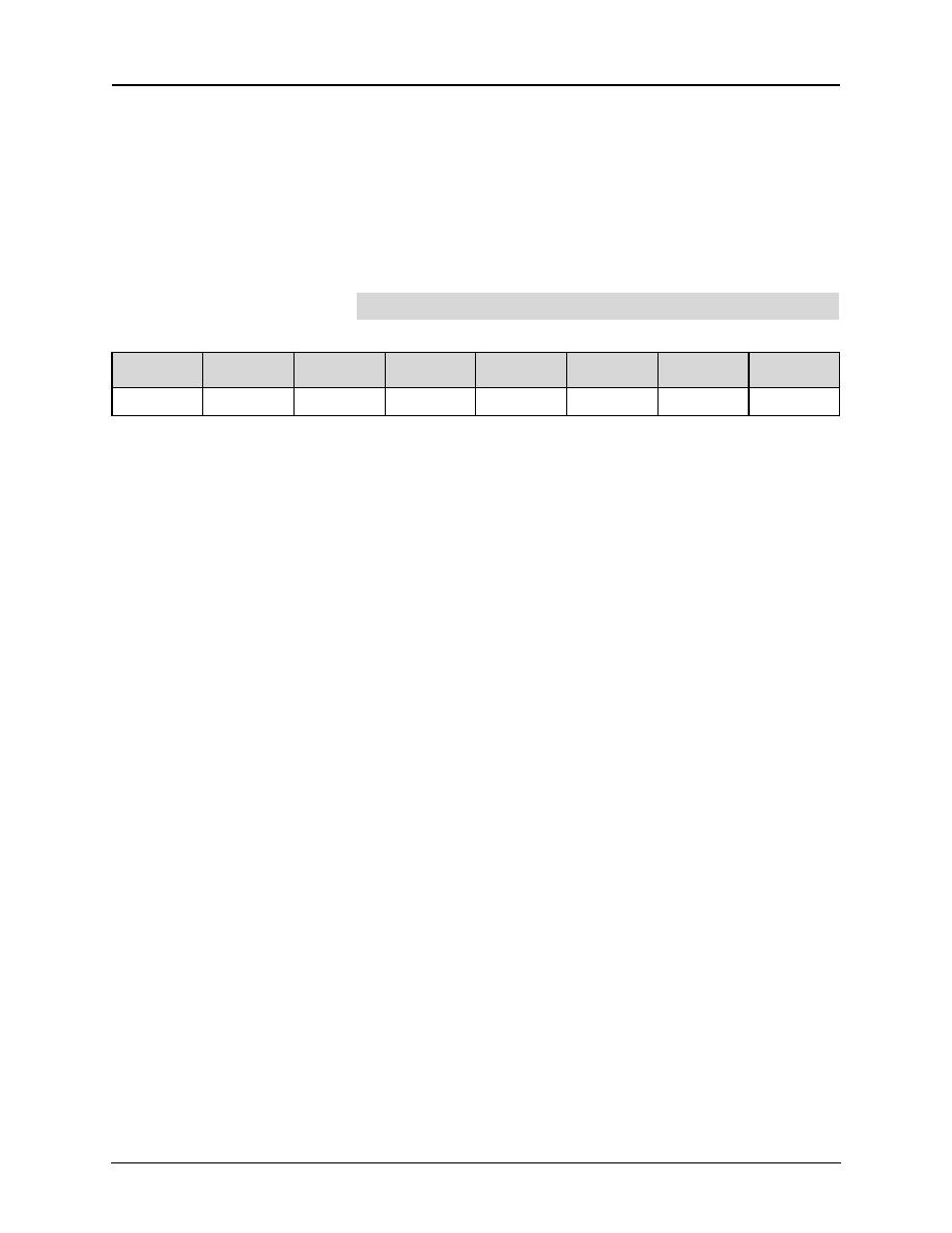
500238B
Mindspeed TechnologiesTM
8
-
111
Advance Information
CX29503 Data Sheet
Register Description
0x5222--Alarm Start Interrupt Enable Register
Writing a 1 to an IER bit allows that specific interrupt source to activate its respective ISR bit in the Alarm Start
Interrupt Status Register [addr: 243], set the appropriate bit in the Interrupt Request Register [addr: 241], and
report the interrupt to the Global Control and Status Block. If cleared, each IER bit allows that source to activate
its respective ISR bit, but prevents activation of the IRR bit and reporting the interrupt to the Global Control and
Status Block.
Default after reset:
00(h)
Direction:
Read/Write
Modification:
Dynamic
SEFStrtIE
Enable SEF Start Interrupt in DS3 mode. This bit has no effect in the E3-G.751 mode.
LOSStrtIE
Enable LOS Start Interrupt in all modes.
IdleStrtIE
Enable Idle Start Interrupt in DS3 mode. This bit has no effect in the E3-G.751 mode.
YelStrtIE
Enable Yellow Alarm Start Interrupt in all modes.
AISStrtIE
Enable AIS Start Interrupt in all modes.
OOFStrtIE
Enable OOF Start Interrupt in all modes.
NOTE:
Reserved bits in the Enable and Control registers must be set to 0.
7
6
5
4
3
2
1
0
Reserved
Reserved
SEFStrtIE
LOSStrtIE
IdleStrtIE
YelStrtIE
AISStrtIE
OOFStrtIE

8-112
Mindspeed TechnologiesTM
500238B
Advance Information
Register Description
CX29503 Data Sheet
0x5223--Alarm End Interrupt Enable Register
Writing a one to an IER bit allows that specific interrupt source to activate its respective ISR bit in the Alarm
End Interrupt Status register [addr: 244], set the appropriate bit in the IRR [addr: 241], and report the interrupt
to the Global Control and Status block. If cleared, each IER bit allows that source to activate its respective ISR
bit, but prevents activation of the IRR bit and reporting the interrupt to the Global Control and Status block.
Default after reset:
00(h)
Direction:
Read/Write
Modification:
Dynamic
LOSEndIE
Enable LOS End Interrupt in all modes.
IdleEndIE
Enable Idle Interrupt End Interrupt in DS3 mode. This bit has no effect in the E3-G.751 mode.
YelEndIE
Enable Yellow Alarm End Interrupt in all modes.
AISEndIE
Enable AIS End Interrupt in all modes.
OOFEndIE
Enable OOF End Interrupt in all modes.
NOTE:
Reserved bits in the Enable and Control registers must be set to 0.
7
6
5
4
3
2
1
0
Reserved
Reserved
Reserved
LOSEndIE
IdleEndIE
YelEndIE
AISEndIE
OOFEndIE
500238B
Mindspeed TechnologiesTM
8
-
113
Advance Information
CX29503 Data Sheet
Register Description
0x5224--Feature1 Control Register
On the CX29503, the line side of the DS3/E3 framer can connect to either the serial line side interface or the
SONET/SDH block. If the interface to the SONET/SDH block is used, then the NRZ mode bit must be set high.
Default after reset:
07(h)
Direction:
Read/Write
Modification:
Bits 0≠2, dynamic; bits 5≠7, static
TxAMI
Transmit AMI mode--Set high to enable AMI line coding on TXPOS and TXNEG (no B3ZS/
HDB3 encoding/decoding). When cleared, B3ZS/HDB3 line coding is used on these signals.
This bit is effective only when the NRZMod bit, in this register, is cleared (see
Table 8-45
).
RxAMI
Receive AMI mode--Set high to enable AMI line coding on RXPOS and RXNEG (no B3ZS/
HDB3 encoding/decoding). When cleared, these signals use B3ZS/HDB3 line coding. This bit
is effective only when the NRZMod bit in this register is cleared (see
Table 8-45
).
NRZMod
NRZ mode--Set high to disable bipolar (B3ZS/HDB3 or AMI) encoding/decoding and
provide a unipolar NRZ line code on TXPOS, TXNEG, RXPOS, and RXNEG. Setting this bit
disables the encoder/decoder circuits and bypasses them. The unipolar output appears at the
TXPOS signal while the TXNEG signal is continuously low and the clock is available on the
TCLKO signal. The unipolar input should appear on RXPOS, while RXNEG can be tied to the
LCV output of the LIU and used as an increment control of the LCV counter.
FEBEC/PT[1:3]
FEBE Pattern/Payload Type Bit Field--In DS3 mode the 3-bit sequence that is sent when a
FEBE indication is transmitted in C-bit parity mode. This pattern is automatically transmitted
when the ExtFEBE/Cj bit in the Transmit Overhead Insertion 1 control register is cleared and
the receiver detects a framing or path parity error. The pattern must be anything other than all
1s to indicate a the FEBE to the far end. An all 1s pattern will disable FEBE transmission and
should not be used for any other purpose.
In both modes, the FEBEC/PT[1] bit is transmitted first and the FEBEC/PT[3] bit is
transmitted last. In both modes, writing a new value to this byte or bit takes effect only starting
from the next transmitted frame.
In DS3-M13/M23 and E3-G.751 modes, this field has no effect.
7
6
5
4
3
2
1
0
TxAMI
RxAMI
NRZMod
Reserved
Reserved
FEBEC/PT[1]
FEBEC/PT[2]
FEBEC/PT[3]
Table 8-45. DS3/E3 Framer Line Side Configurations
NRZMod
RxAMI
TxAMI
Configuration
0
0
X
B3ZS/HDB3 encoded data on RXPOS, RXNEG
0
1
X
AMI encoded data on RXPOS, RXNEG
0
X
0
B3ZS/HDB3 encoded data on TXPOS, TXNEG
0
X
1
AMI encoded data on TXPOS, TXNEG
1
X
X
NRZ data on TXPOS, RXPOS; TXNEG is set to 0; RXNEG is used as
an LCV input from the LIU (if unused, should be tied low)

8-114
Mindspeed TechnologiesTM
500238B
Advance Information
Register Description
CX29503 Data Sheet
0x5225--Feature2 Control Register
On the CX29503, the system side of the DS3/E3 framer can connect to either the TSB interface or the M13
block.
Default after rest:
01(h)
Direction:
Read/Write
Modification:
Bit 5, dynamic; bits 0≠4, static
TxLOS
Transmit LOS--This bit, while set, results in the generation of all 0s (LOS) on the transmit
line side. Setting this bit overrides any other programmed/inserted payload and overhead
pattern with 0s.
TxOvhMrk
Transmit Overhead Bits Mark--This bit controls the behavior of the TXSY signal when
programmed to be driven as an output. When set, TXSY marks the bit positions of all overhead
bits. When cleared, TXSY marks the beginning of a new frame.
TXSYOut
TXSY Signal Output Control--This bit determines if the TXSY signal is an output of the chip.
When set, this signal is an output, i.e., the transmitter circuit generates its own frame
synchronization mechanism and signals the frame start or the overhead bit positions
(according to TxOvhMrk bit) on the TXSY signal to the system. When cleared, TXSY can be
an input or undefined according to the value of the TXSYIn bit in this register.
During and after reset, TXSY drives high Z, and is neither in output state nor in input state.
TXSYIn
TXSY Signal Input Control--This bit determines if the TXSY signal is an input of the chip.
When set, this signal is an input, i.e., the system generates a synchronization pulse and the
transmitter circuit acts according to it. When cleared, TXSY can be an output or undefined
according to the value of the TXSYOut bit in this register.
During and after reset, TXSY drives high Z, and is neither in output state nor in input state.
TxInvClk
Transmit System Side Inverted Clocks--This bit controls the polarity of TXGAPCK and
TEXTCK output clocks. When the bit is cleared, TXGAPCK and TEXTCK rising edges are
derived from TXCKI falling edge. In this mode, both clock gaps are active-low. When this bit
is set, TXGAPCK and TEXTCK are inverted, hence TXGAPCK and TEXTCK falling edges
are derived from TXCKI falling edge. In this mode, both clock gaps are active high.
LTxCkRis
LIU Transmit Clock Polarity Control--Used to define the TCLKO edge upon which the
transmitter output data (on TXPOS, TXNEG signals) is sampled by the LIU. When set, the
data is clocked out by the chip on the falling edge of TCLKO. It is sampled by the LIU on the
rising edge of TCLKO. When cleared, the data is clocked out by the chip on the rising edge of
TCLKO; therefore, it is sampled by the LIU on the falling edge of TCLKO.
7
6
5
4
3
2
1
0
Reserved
Reserved
TxLOS
TxOvhMrk
TXSYOut
TXSYIn
TxInvClk
LTxCkRis
NOTE:
TXSYOut and TXSYIn bits should not be set at the same time.
NOTE:
TXSYOut and TXSYIn bits should not be set at the same time.

500238B
Mindspeed TechnologiesTM
8
-
115
Advance Information
CX29503 Data Sheet
Register Description
0x5226--Feature3 Control Register
Default after reset:
00(h)
Direction:
Read/Write
Modification:
Bit 4, static; bits 0≠2 and 5≠7, dynamic
PayldLp
Payload Loopback Enable--Set to enable a payload loopback from the receiver circuit through
the transmitter circuit back to the network. This loopback connects the received payload (after
decoding, frame recovery, and overhead extraction) to the transmitter input, where it is framed
and encoded again. The received data is still present on the receiver output signals.
A dynamic change of this bit can cause loss of data for a few clock cycles, until the channel is
internally synchronized. Activation/deactivation of a loopback causes internal circuits to
switch between clocks. After writing to this bit, the microprocessor should not access any of
the device registers (read or write) for the 20 slowest clock cycles.
RlineLp
Remote Line Loopback Enable--Set to enable loopback after decoding/encoding back to the
network. If the receiver FIFO is disabled (the RxFIFEn bit in the Feature5 register is clear) data
output of the B3ZS/HDB3 decoder connects to the transmitter encoder input. If the receiver
FIFO is enabled (RxFIFEn bit is set), data output of this FIFO connects to the transmitter
encoder input. LCVs are not preserved in this loopback. The received data is still presented to
all receiver blocks and is present on the receiver outputs.
A dynamic change of this bit can cause loss of data for a few clock cycles, until the channel is
internally synchronized. Activation/deactivation of a loopback causes internal circuits to
switch between clocks; after writing to this bit, the microprocessor should not access any of the
device registers (read or write) for the 20 slowest clock cycles.
TxFEACIE
Transmit FEAC Interrupt Enable--A control bit allows interrupts from the FEAC transmitter
when in DS3-C Bit Parity mode. When in single mode, the interrupt is asserted after every
transmission of the code word written in the Transmit FEAC Channel Byte register. When in
repetitive mode, the interrupt is asserted once the code word is transmitted 10 times. The
associated interrupt status is reported in TxFEACItr bit in the Transmit Data Link FEAC
Interrupt Status register [addr: 248].
FEACSin
FEAC Channel in Single Mode--DS3-C Bit Parity mode set to enable FEAC channel (in the
transmitter and the receiver) in a single mode, i.e., assert an interrupt after a single reception/
transmission of a code word. When clear, a repetitive mode is enabled, i.e., an interrupt is
asserted after completion of 10 repetitions of code word reception/transmission. In DS3-M13/
M23 and E3-G.751 modes, this bit has no effect.
RxFEACSNEIE
Receive FEAC Stack Not Empty Interrupt Enable--A control bit that allows interrupts due to
detection of the FEAC stack being "not empty", i.e., the Receive FEAC stack byte is holding
valid data. Active both in single and repetitive modes. The associated interrupt status is
reported in the RxFEACSNE bit in the Receive FEAC Interrupt Status register [addr: 251].
RxFEACIdleIE
Receive FEAC Channel Idle Interrupt Enable--A control bit that allows interrupts due to
detection of the start of an idle pattern over an FEAC channel by the receiver circuit. Active
both in single and repetitive modes. The associated interrupt status is reported in the
RxFEACIdle bit in the Receive FEAC Interrupt Status register [addr: 251].
7
6
5
4
3
2
1
0
PayldLp
RlineLp
TxFEACIE
FEACSin
Rsvd
RxFEACSNEIE
RxFEACIdleIE
RxFEACIE

8-116
Mindspeed TechnologiesTM
500238B
Advance Information
Register Description
CX29503 Data Sheet
RxFEACIE
Receive FEAC Interrupt Enable--A control bit that allows interrupts from the FEAC receiver
when in DS3-C Bit Parity mode. When a legal code word is detected by the receiver, the
interrupt is asserted. The associated interrupt status is reported in the RxFEACItr bit in the
Receive FEAC Interrupt Status register [addr: 251].
0x5227--Feature4 Control Register
This control register has an effect only in E3-G.832 mode. Because the CX29503 does not support E3-G.832
mode, this register is reserved and must be maintained at its initial value of 0x00.
Default after reset:
00(h)
SSMEn
SSM Mode Enable
SSM[1]/TM
SSM MSB/Timing Marker Bit Field
SSM[2:4]
SSM Bit Field
MAPD[1:2]
Payload Dependent Field in MA Byte
0x5228--Feature5 Control Register
Default after rest:
00(h)
Direction:
Read/Write
Modification:
Bits 4≠6, dynamic; bits 0≠3, 7-static
RxAutoAll
Receive Automatic All 1s on Data Stream--Set to enable automatic generation of an all-1s
stream on RXDAT signal in response to a fault detection. When set and LOS, OOF, AIS, or
Idle are detected in DS3 mode or LOS, OOF, or AIS are detected in E3 mode, the data received
on RXPOS, RXNEG is presented to the receiver circuit, but is not present on RXDAT signal. It
is overwritten by an all-1s stream. The automatic all-1s assertion continues as long as one or
more of these conditions is valid.
When clear, all 1s sequences on the RXDAT signal occurs due to the RxAll1 bit in this register.
RxAll1 and RxAIS bits in this register have precedence over this bit and affect the RX data
stream.
RefrmStp
Reframe Mechanism Stop--This bit controls the behavior of the frame-search mechanism.
When this bit is set (=1), no frame-search is conducted (regardless of OOF status); when it has
been cleared (0 is written over a previous 1), frame-search resumes, shifted forward by 1 bit
from the current frame position, until a new framing is located. When it is cleared (=0),
searching occurs in response to an OOF status.
7
6
5
4
3
2
1
0
Reserved
SSMEn
SSM[1]/TM
SSM[2]
SSM[3]
SSM[4]
MAPD[1]
MAPD[2]
7
6
5
4
3
2
1
0
RxAutoAll1
RefrmStp
RxAIS
RXAll1
RxOvhMrk
RxFIFEn
RxInvClk
LRxCkRis
NOTE:
To produce a "forced reframe", the microprocessor will usually need 2 write cycles,
the first to write 1 to the bit, the next to write 0 to it.

500238B
Mindspeed TechnologiesTM
8
-
117
Advance Information
CX29503 Data Sheet
Register Description
RxAIS
Receive Data Stream AIS--Set to enable driving of an AIS pattern (in all DS3 and E3 modes)
on the RXDAT signal. When set, data received on RXPOS and RXNEG is presented to the
receiver circuit, but is not present on the RXDAT signal. Detection and count of errors, alarms,
and events continues while this mode operates. When cleared, data received on RXPOS and
RXNEG, and processed by the receiver circuit, is present on the RXDAT signal. If both
RxAll1 and RxAIS are active, a data stream of all 1s is generated.
RxAll1
Receive Data Stream is All 1s--Set to enable driving of an unchannelized all-1s stream on the
RXDAT signal. When set, data received on RXPOS and RXNEG is presented to the receiver
circuit, but is not present on the RXDAT signal. Detection and count of errors, alarms, and
events continues while this mode is operated. When cleared, the data received on RXPOS and
RXNEG, and processed by the receiver circuit, is present on the RXDAT signal. If both
RxAll1 and RxAIS are active, a data stream of all 1s is generated.
RxOvhMrk
Receive Overhead Bits Mark--This bit controls behavior of the RXMSY signal. When set,
RXMSY marks the bit positions of all overhead bits (framing and C bits). When cleared,
RXMSY marks the beginning of a new frame.
RxFIFEn
Receiver FIFO Enable --Set to enable usage of the receiver FIFO buffer to provide jitter
elasticity to the input data stream. When set, data output of the B3ZS/HDB3 decoder is
sampled into the FIFO buffer using the LINECK clock. It is taken out of the FIFO buffer
according to the RXCKI clock. When cleared, the FIFO buffer is bypassed. Data goes from the
decoder directly into the frame recovery circuit and the only clock used in the receiver circuitry
is LINECK. Activation/deactivation of the FIFO buffer causes internal circuits to switch
between clocks; after writing to this bit, the microprocessor should not access any of the device
registers (read or write) for the 20 slowest clock cycles.
RxInvClk
Receive System Side Inverted Clocks--This bit controls the polarity of the RXGAPCK and
REXTCK output clocks. When the bit is cleared, RXGAPCK and REXTCK rising edges are in
parallel to the data change on RXDAT signal. In this mode, both clocks gaps are active-low.
When this bit is set, RXGAPCK and REXTCK are inverted. The RXGAPCK and REXTCK
falling edges are parallel to the data change on RXDAT signal. In this mode, both clocks gaps
are active-high.
LRxCkRis
LIU Receive Clock Polarity Control--Used to define the LINECK edge upon which the
receiver input data (on RXPOS, RXNEG signals) is clocked out by the LIU. When set, the data
is sampled by the chip on the falling edge of LINECK, therefore, it is clocked out by the LIU
on the rising edge of LINECK. When clear, data is sampled by the chip on the rising edge of
LINECK, therefore, it is clocked out by the LIU on the falling edge of LINECK.

8-118
Mindspeed TechnologiesTM
500238B
Advance Information
Register Description
CX29503 Data Sheet
0x5229--Transmit Overhead Insertion1 Control Register
The Transmit Overhead Insertion Control register enables insertion of different overhead fields from the
following different sources:
!
Internal automatic generation
!
Internal registers programmed by the microprocessor
!
The system via the data stream
!
The system via the TSB interface (only DL data)
The TSB interface on the CX29503 only supports the transfer of the terminal Data Link (DL) channel. For DS3
C-bit parity, the DL channel resides on the C5 bits; for E3-G.751, it resides on the N-bit.
Default after reset:
00(h)
Direction:
Read/Write
Modification:
Bits 0≠2 and 4≠5, static; bits 6≠7, dynamic; bit 3, dynamic for Cj and static for FEBE
DLMod[2:0]
Data Link Mode--This field is interpreted differently in the different working modes. In E3-
G.751, only DLMod[2:1] determines the source of the N-bit, while DLMod[0] has no effect. In
DS3-C-bit parity mode, DLMod[2:1] determines the source of the data link (Cb5) and
DLMod[0] determines the source of the reserved C bits. In DS3-M13/M23, this field has no
effect.
Table 8-46
details the interpretation of this field in the E3-G.751 mode.
NOTE:
Not all the sources are available for every overhead field in every mode. Some of the
control bits have no effect in a specific mode. Some of the bits have multiple
meanings, depending on the working mode.
7
6
5
4
3
2
1
0
DLMod[2]
DLMod[1]
DLMod[0]
AutoRAI
ExtFEBE/Cj
ExtCP/TR
ExtFEAC/PD
ExtDat
NOTE:
If the system wishes to change the source of the data link, it must first disable the
data link and then enable it by setting the appropriate mode.
Table 8-46. DS3-C Bit Parity/E3-G.751 Mode Field Interpretation
DLMod[2]
DLMod[1]
Description
0
X
The Transmit Data Link circuit is disabled and the framer automatically sends
the all-1s pattern on the Cb5 bits/N-bit.
1
0
DL data is inserted through transmit data link FIFO buffer and is processed by
the internal HDLC circuit.
1
1
DL data is inserted through the TSB interface and is unaffected by the internal
HDLC circuit.

500238B
Mindspeed TechnologiesTM
8
-
119
Advance Information
CX29503 Data Sheet
Register Description
DS3-C Bit Parity
DLMod[0] controls the reserved C-bits (C12, Cb2, Cb6, Cb7) generation. When cleared, these
bits are automatically generated as all 1s. This bit must not be set because the CX29503 does
not support the transfer of the reserved C bits over the TSB interface.
AutoRAI
Automatic RAI/RDI generation control--Set to enable automatic generation of the RAI or
RDI alarm in response to a fault detection. When set, an automatic assertion of RAI in E3-
G.751 mode occurs once the receiver detects an LOS or OOF condition. The automatic
assertion continues as long as one or more of these conditions is valid. The TxAlm[1] bit in the
Mode Control register still affects RAI/RDI generation in E3 mode while this bit is set. When
clear, RAI/RDI generation occurs due to the TxAlm[1] bit in the Mode Control register, and
there is no automatic generation.
ExtFEBE/Cj
External FEBE/Justification Control--Must be cleared because the CX29503 does not support
the insertion of FEBE or justification control bits via the TSB interface.
ExtCP/TR
External CP/Timing Marker/SSM Control--In DS3-C Bit Parity mode, this bit must be
cleared because the CX29503 does not support the insertion of CP bits or TR byte via TSB
interface mode. In DS3-M13/M23 and E3-G.751 modes, this bit has no effect.
ExtFEAC/PD
External FEAC/Payload Dependent/Multiframe Indicator Field Control--In DS3-C Bit Parity
mode, this bit must be cleared because the CX29503 does not support the insertion of an
FEAC channel via the TSB interface. When this bit is cleared, the FEAC channel is inserted
through a programmable register (Transmit FEAC Channel Byte) in DS3-C Bit Parity mode. In
DS3-M13/M23 and E3-G.751 modes, this bit has no effect.
ExtDat
External Data Control--Set to enable all overhead bits to be inserted via the data stream.
When set, this bit overrides the rest of the control bits in this register. It disables internal
generation of overhead bits (automatic or through programmable registers) and forces the chip
to use the overhead bits inserted in the data stream of the Transmit Overhead Insertion2
Control register. When clear, overhead configuration is determined by the rest of the control
bits as described above. This bit affects all modes. Setting of TxAlm[1:0] bits is effective even
during ExtDat = 1.
NOTE:
This bit has no effect in DS3 mode. Generation of an RAI alarm in DS3 mode is
controlled only by TxAlm bits.

8-120
Mindspeed TechnologiesTM
500238B
Advance Information
Register Description
CX29503 Data Sheet
0x522A--Transmit Overhead Insertion2 Control Register
The Transmit Overhead Insertion Control registers enable insertion of different overhead fields via the TEXT
signal. On the CX29503, the TEXT signal is an output from the TSB block to the D3/E3 block. This signal is
only used to pass the data for the terminal DL channel. See
Figure 8-4
for the TSB block to DS3/E3 block
interface.
NOTE:
Not all the sources are available for every overhead field in every mode. Some of the
control bits have no effect in a specific mode. Some of the bits have multiple
meanings, depending on the working mode.
Figure 8-4. TSB Module to DS3/E3 Module Interface
TSB Module
DS3/E3 Framer
P
a
y
l
o a
d
P
a
y
l o
a
d
O
v
e
r
h
e a
d
O
v
e
r
h e
a
d
RXDAT
RXGAPCK
(g aped clock)
TXGAPCK
(g aped clock)
TXDATI
REXTCK
(g aped clock)
TEXTCK
(g aped clock)
TEXT
Source:
DS3 44.736 M Hz
E3 34.368 MHz
m 13_rxgap
ck
m 13_txgap
ck
tsb_txda
ti
m 13_rextc
k
m 13_textc
k
tsb_tex
t
m 13_rxd
at
TS
B
TXCKI
RXCKI

500238B
Mindspeed TechnologiesTM
8
-
121
Advance Information
CX29503 Data Sheet
Register Description
Default after reset:
00(h)
Direction:
Read/Write
Modification:
Static
ExtStf
External stuff bits--Must be cleared on the CX29503 in DS3-M13/M23 and E3-G.751 modes.
When clear, stuff bits are inserted with the payload. This bit has no affect in DS3-C Bit Parity
mode.
ExtFrmAl
External Frame Alignment bits--Must be cleared on the CX29503. When clear, the frame
alignment bits are automatically generated by the internal circuitry.
ExtP
External P-Bit control--Must be cleared on the CX29503 in DS3-C Bit Parity and DS3-M13/
M23 modes. When clear, P-bits are automatically calculated by the internal circuitry. In E3-
G.751 mode, this bit has no effect.
ExtRAI
External X/A/RDI-Bit control--Must be cleared on the CX29503 to disable insertion of X-bits
(in DS3), and A-bits (in E3-G.751) because this data is not provided on the TEXT input.
7
6
5
4
3
2
1
0
Reserved
Reserved
Reserved
Reserved
ExtStf
ExtFrmAl
ExtP
ExtRAI

8-122
Mindspeed TechnologiesTM
500238B
Advance Information
Register Description
CX29503 Data Sheet
0x522B--REXTCK Control Register
The REXTCK Control register provides for the marking of different fields through the REXTCK signal. On the
CX29503, the REXTCK signal is an output from the DS3/E3 block to the TSB block. This signal is only used to
clock the data for the terminal data link channel (DL) that is transferred on the RXDAT signal.
The DL field should be disabled from being presented on RXGAPCK interface in the Receive Overhead
Control register [addr: 22C].
Default after reset:
00(h)
Direction:
Read/Write
Modification:
Static
ExtReserved/GC
External Reserved C bits/GC byte--Must be cleared on the CX29503.
In DS3-C Bit Parity mode, clearing this bit disables the presentation of reserved C bits (C12,
C2, C6, C7) through the REXTCK signal. In DS3-M13/M23 and E3-G.751 modes, this bit is
ignored.
ExtDL/NR
External Data Link/NR byte--Can be set or cleared on the CX29503.
This bit enables presentation of data link data through the REXTCK signal. The bits are output
exactly as received, i.e., the HDLC circuit is bypassed. In DS3-C Bit Parity mode, this bit
enables presentation of C5 bits through the TSB interface. In E3-G.751 mode, this bit enables
presentation of N-bit through the TSB interface. In DS3-M13/M23, this bit is ignored.
ExtFEBE/A
External FEBE/REI/A-bit--Must be cleared on the CX29503.
This bit enables presentation of FEBE field in DS3-C Bit Parity mode through the REXTCK
signal. In E3-G.751 mode, set to enable presentation of A-bit through REXTCK signal. In
DS3-M13/M23 mode, this bit is ignored.
ExtCP/TM
External Path Parity/Timing Marker/SSM--Must be cleared on the CX29503.
This bit enables presentation of the CP field in DS3-C Bit Parity mode through the REXTCK
signal. In DS3-M13/M23 and E3-G.751 modes, this bit is ignored.
ExtFEAC/PD/Stf
External FEAC/Payload Dependent/Multiframe Indicator/Stuff Opportunity bits--Must be
cleared on the CX29503. This bit enables presentation of the FEAC channel in DS3-C Bit
Parity mode or stuff opportunity bits in DS3 M13/M23 and in E3-G.751 modes through the
REXTCK signal.
ExtAIC/Cj/TR
External AIC/Justification Control/Trail Trace--Must be cleared on the CX29503.
In DS3-C Bit Parity mode, this bit enables presentation of the application identification
channel through REXTCK signal. In DS3-M13/M23 and E3-G.751 modes, set this bit to
enable presentation of the justification control bits through the REXTCK signal.
ExtFrm
External Framing fields--Must be cleared on the CX29503. In DS3 modes, this bit enables
presentation of M, F, X, and P bits through the REXTCK signal. In E3-G.751 mode, set this bit
to enable presentation of FAS field through the REXTCK signal.
AllRxExt
All Received data is External--Must be cleared on the CX29503. This bit enables presentation
of the complete frame, i.e., payload and overhead bits, through the REXTCK signal. This bit is
available in all framing modes. When this bit is set, it overrides the rest of the bits in this
register. Presentation of overhead bits through the RXGAPCK signal or through the
microprocessor interface in parallel to REXTCK is determined by the Receive Overhead
Control register and by the RxDLEn bit in the Receive Data Link Control register.
7
6
5
4
3
2
1
0
ExtReserved/GC
ExtDL/NR
ExtFEBE/A
ExtCP/TM
ExtFEAC/PD/Stf
ExtAIC/Cj/TR
ExtFrm
AllRxExt

500238B
Mindspeed TechnologiesTM
8
-
123
Advance Information
CX29503 Data Sheet
Register Description
0x522C--Receive Overhead Control Register
On the CX29503, the RXGAPCK signal is an output from the DS3/E3 block to the TSB block. This signal is
used to clock the payload data that is transferred on the RXDAT signal.
Default after reset:
00(h)
Direction:
Read/Write
Modification:
Static
RxStfDat
Received Stuff Opportunity bits in the Data steam--Set to enable presenting the Stuff
Opportunity bits in the data stream over the RXDAT signal in DS3-M13/M23 and E3-G.751
modes. When set, RXGAPCK is not gapped over the Stuff Opportunity bit positions. When
clear, the Stuff Opportunity bits are not extracted, i.e., RXGAPCK is gapped over their bit
positions. When the AllOVHDat bit in this register is set, this bit is ignored. In DS3-C Bit
Parity mode, this bit is ignored.
RxCjDat
Received Justification Control bits in the Data stream--Set to enable presenting the
justification control bits in the data stream over the RXDAT signal in DS3-M13/M23 and E3-
G.751 modes. When set, RXGAPCK is not gapped over the Justification Control bit positions.
When clear, the Justification Control bits are not extracted, i.e., RXGAPCK is gapped over
their bit positions. When the AllOVHDat bit in this register is set, this bit is ignored. In DS3-C
Bit Parity mode, this bit is ignored.
AllOVHDat
All Overhead bits are in the Data stream--Set to enable presenting the complete frame in the
data stream over the RXDAT signal, i.e., RXGAPCK is a nominal clock (it is not gapped). This
bit is available in all framing modes. When this bit is set, it overrides the RxCjDat bit in this
register. When this bit is cleared, presenting the Justification Control bits on RXDAT
(RXGAPCK gapping over Cj bit positions) is determined by the RxCjDat bit in this register.
Other overhead bits are not presented on the RXDAT signal when this bit is cleared, i.e.,
RXGAPCK is gapped accordingly.
Table 8-47
details RXGAPCK output behavior in different modes according to the listed bits settings.
7
6
5
4
3
2
1
0
Reserved
Reserved
Reserved
Reserved
Reserved
RxStfDat
RxCjDat
AllOVHDat
Table 8-47. Summary of RXGAPCK Options
RxStfDat
RxCjDat
AllOVHDat
RXGAPCK Output Behavior
X
X
1
Nominal
0
0
0
Tick on Payload bits only (not on Stuff Opportunity bits)
0
1
0
Ticks only on Payload bits and Justification Control bits (in DS3-
M13/M23 and E3-G.751)
1
0
0
Ticks only on Payload bits and Stuff Opportunity bits (in DS3-M13/
M23 and E3-G.751)
1
1
0
Ticks on Payload, Stuff Opportunity, and Justification Control bits
(in DS3-M13/M23 and E3-G.751)
8-124
Mindspeed TechnologiesTM
500238B
Advance Information
Register Description
CX29503 Data Sheet
0x522D--Transmit Data Link Control Register
The Transmit Data Link (DL) Control register (CR13i) enables different modes and interrupts in the transmit
data link operation.
Default after reset:
00(h)
Direction:
Read/Write
Modification:
Bits 1≠3, dynamic; bits 0, DL-static
TxMsgIE
Transmit DL Message Transmitted Interrupt Enable--Enable interrupt due to end-of-
transmission of a full message.
TxURIE
Transmit DL FIFO Underrun Interrupt Enable--Enable due to data link FIFO underrun error.
TxNEIE
Transmit DL FIFO Near-Empty Interrupt Enable--Enable interrupt due to the FIFO buffer
being near empty.
TxFCSEn
Transmit DL FCS Calculation Enable--Set to enable an FCS calculation over the transmitted
message and add it to the end of the transmitted message. When cleared, the FCS calculation
and addition are executed by the software.
0x522E--Transmit Data Link Threshold Control Register
Default after reset:
00(h)
Direction:
Read/Write
Modification:
DL-static
TxNEThr[6:0]
Transmit DL FIFO Near-Empty Threshold--Set to the threshold value, used to indicate a near-
empty FIFO event. The range of values available for this purpose is 0≠126, when 00(h) is
interpreted as 0, 01(h) is 1, etc., and 7E(h) is interpreted as 126.
NOTE:
Reserved bits in control registers must be set to 0.
7
6
5
4
3
2
1
0
Reserved
Reserved
Reserved
Reserved
TxMsgIE
TxURIE
TxNEIE
TxFCSEn
7
6
5
4
3
2
1
0
Reserved
TxNEThr[6]
TxNEThr[5]
TxNEThr[4]
TxNEThr[3]
TxNEThr[2]
TxNEThr[1]
TxNEThr[0]

500238B
Mindspeed TechnologiesTM
8
-
125
Advance Information
CX29503 Data Sheet
Register Description
0x522F and 0x5230--Transmit Data Link Message Byte
(Lower Address and Higher Address)
Default after reset:
Undefined
Direction:
Read/Write
Modification:
Dynamic
TxDLMsg[7:0]
Transmit DL Message byte--This byte is loaded with data to be written into the data link FIFO
buffer, and is later transmitted by the data link transmitter circuit. Two addresses are allocated
for this register. During the entire message, excepting the last byte of the message, the lower
address is used to access this register. When the last byte of the message is written to this
register, the higher address is used. Using the higher address indicates the end of the message
to the transmitter circuit.
The TxDLMsg[0] bit is transmitted first and the TxDLMsg[7] bit is transmitted last. Reading
this register causes latching of the content of the FIFO stage pointed by the Transmit DL Read
Pointer into this register.
0x5231--Receive Data Link Control Register
The Receive Data Link Control register enables operation of the receiver terminal data link circuit, defines the
FCS mode, and enables interrupt assertion due to data link events.
Default after reset:
00(h)
Direction:
Read/Write
Modification:
Bits 0, 2≠4--dynamic; bits 1, 5--DL-static
NRDL
NR Byte over the DL--This bit is effective only in E3-G.832 mode and is reserved for the
CX29503 application and must be maintained low.
RxOVRIE
Receive DL FIFO Overrun Interrupt Enable--Set to enable interrupt assertion due to data link
FIFO overrun error.
RxMsgIE
Receive DL Message Interrupt Enable--Set to enable interrupt assertion due to a message
received event.
RxNFIE
Receive DL FIFO Near-Full Interrupt Enable--Set to enable interrupt assertion due to the
FIFO near-full event.
7
6
5
4
3
2
1
0
TxDLMsg [7]
TxDLMsg [6]
TxDLMsg [5]
TxDLMsg [4]
TxDLMsg [3]
TxDLMsg [2]
TxDLMsg [1]
TxDLMsg [0]
NOTE:
Reserved bits in control registers must be set to 0.
7
6
5
4
3
2
1
0
Reserved
Reserved
NRDL
RxOVRIE
RxMsgIE
RxNFIE
RxFCSEn
RxDLEn

8-126
Mindspeed TechnologiesTM
500238B
Advance Information
Register Description
CX29503 Data Sheet
RxFCSEn
Receive DL FCS check Enable--Set to enable execution of an FCS check on the received
message. When cleared, the FCS check is executed by software; therefore, no interrupt or
status due to bad FCS will appear.
RxDLEn
Receive DL Enable--Set to enable operation of the receive data link FIFO buffer and HDLC/
LAPD circuits over the selected data link channel (Cb5 or N-bit or NR or GC). When cleared,
the data link channel data is left unchanged (may be presented on the data stream via the
REXTCK and RXGAPCK clocks), and no receive datalink interrupts (enabled in this register)
are asserted.
0x5232--Receive Data Link Threshold Control Register
Default after reset:
7F(h)
Direction:
Read/Write
Modification:
DL-static
RxNFThr[6:0]
Receive DL FIFO Near-Full Threshold--Set to the threshold value, used to indicate a near-full
FIFO event. The range of values available for this purpose is 2≠127, when 02(h) is interpreted
as 2 and 7F(h) is interpreted as 127.
0x5233--Transmit FEAC Channel Byte
Default after reset:
FF(h)
Direction:
Read/Write
Modification:
Dynamic
TxFEAC[7:0]
Transmit FEAC Channel Message Byte--If the mode is set to DS3-C Bit Parity, this register is
used as the data byte for the Transmit FEAC channel transmitter. When this byte is in the form
'0xxxxxx0', it is transmitted after every flag. If there is a 1 in either the most significant or least
significant bit of this register, all 1s (idle) will be transmitted on the FEAC channel. An
interrupt is associated with this channel and is enabled by the TxFEACIE bit in the Feature3
control register. The TxFEAC[0] bit is transmitted first and the TxFEAC[7] bit is transmitted
last.
7
6
5
4
3
2
1
0
Reserved
RxNFThr [6]
RxNFThr [5]
RxNFThr [4]
RxNFThr [3]
RxNFThr [2]
RxNFThr [1]
RxNFThr [0]
7
6
5
4
3
2
1
0
TxFEAC[7]
TxFEAC[6]
TxFEAC[5]
TxFEAC[4]
TxFEAC[3]
TxFEAC[2]
TxFEAC[1]
TxFEAC[0]

500238B
Mindspeed TechnologiesTM
8
-
127
Advance Information
CX29503 Data Sheet
Register Description
0x5240--DS3/E3 Maintenance Status Register
The DS3/E3 Maintenance Status register contains the major DS3/E3 maintenance indicators.
Value after reset:
81(h)
Direction:
Read only
Value after enable:
If the RefrmSbp bit is clear--18(h). If the RefrmSbp bit is set--01(h).
ReFrm
Reframe In-Progress--Set while the framing circuit searches for a valid framing pattern in
either DS3 or E3 modes.
LOSAlm
Loss-Of-Signal (LOS) Alarm--Indicates that the received signal prior to B3ZS/HDB3
decoding has been lost. This signal is set as soon as the receiver detects the LOS condition and
clears when the receiver detects a legal signal.
IdleDet
Idle Code Detect--Set if an idle pattern is found. This bit is low in E3 modes because there is
no defined E3 idle signal.
YelDet
Yellow Alarm Detect--Set when an RAI/RDI event is detected in the receiver.
AISDet
Alarm Indication Signal (AIS) Detect--Set if the receiver detects an AIS event.
OOFAlm
Out-Of-Frame (OOF) Alarm--Set when an OOF condition is detected by the receiver. This
condition will initiate a reframe.
0x5241--Interrupt Request Register (IRR)
An IRR bit is latched active (high) whenever an enabled interrupt source reports an interrupt event in the
corresponding status register. The IRR is latched until the corresponding ISR register is read by the processor.
Reading the ISR clears the respective IRR bit independently of clearing ISR bits. Therefore, persistently active
ISR bits will not affect INTR* deactivation.
All IRR bits are logically ORed to activate a corresponding bit in the DS3/E3 bit in the Top Level Interrupt
Status register. The processor must read IRR = 00 before exiting its interrupt service routine to confirm that all
the DS3/E3 Interrupt Request Register bits have been deasserted.
See
Figure 8-5
for the DS3/E3 Framer interrupt structure. It requires searching 3 levels to respond to an
interrupt request.
!
Top Level--contains the interrupt request status from the DS3/E3 framer.
!
Second Level--contains the interrupt request from 6 functional blocks in the DS3/E3 framer. One register
read is required to determine which functional block is requesting service.
!
Third Level--contains the interrupt source within the particular functional block. One register read is
required before servicing the request.
7
6
5
4
3
2
1
0
ReFrm
Reserved
Reserved
LOSAlm
IdleDet
YelDet
AISDet
OOFAlm
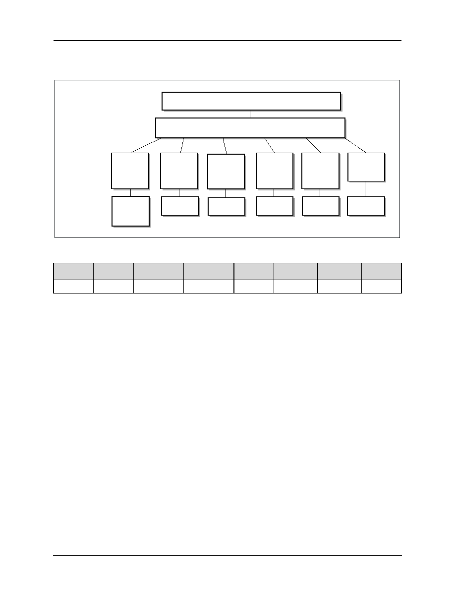
8-128
Mindspeed TechnologiesTM
500238B
Advance Information
Register Description
CX29503 Data Sheet
Value after reset:
00(h)
Direction:
Read only
Value after enable:
Unaffected (affected indirectly by other registers)
TxDLFEACItr
Transmit Data Link/FEAC Interrupt Source--Set if one or more of the interrupt-related active
status bits in the Transmit Data Link FEAC Status register are high. Cleared when the bits
related to interrupt activation in the Transmit Data Link FEAC Status register or their interrupt
masks are low.
RxDLltr
Receive Data Link Interrupt Source--Set if one or more on the interrupt-related active status
bits in the Receive Data Link Status register are high. Cleared when the bits related to interrupt
activation in the Receive Data Link Status register or their interrupt masks are low.
RxFEACltrs
Receive FEAC Interrupt Source --Set if one or more of the interrupt-related active status bits
in the Receive FEAC Status register are high. Cleared when the bits related to interrupt
activation in the Receive FEAC Status register or their interrupt masks are low.
AlarmEndItr
Alarm End Interrupt2 Source--Set if one or more of the active status bits in the Alarm End
Interrupt Status register are high. Cleared when the bits related to interrupt activation in the
Alarm End Interrupt Status register or their interrupt masks are low.
AlarmStrtItr
Alarm Start Interrupt Source--Set if one or more of the active status bits in the Alarm Start
Interrupt Status register are high. Cleared when the bits related to interrupt activation in the
Alarm Start Interrupt Status register or their interrupt masks are low.
Ctrltr
Counter Interrupt Source--Set if one or more of the active status bits in the Counter Interrupt
Status register are high. Cleared when the bits related to interrupt activation in the Counter
Interrupt Status register or their interrupt masks are low.
Figure 8-5. DS3/E3 Framer Interrupt Structure
(x221)
Counter
ISR
(x242)
Alarm
Start
ISR
(x243)
Alarm
End
ISR
(x244)
RDL
ISR
(x24B)
Interrupt Request Register (x241)
Top Level Interrupt Status Register
Rx FEAC
ISR
(x251)
Top Level
2nd Level
3rd Level
TDL and
Tx FEAC
ISR
(x248)
Enable
Registers
(x226
and
x22D)
(x231)
(x226)
(x223)
(x222)
100702_042
7
6
5
4
3
2
1
0
Reserved
Reserved
TxDLFEACItr
RxDLltr
RxFEACltrS
AlarmEndItr
AlarmStrtItr
Ctrltr

500238B
Mindspeed TechnologiesTM
8
-
129
Advance Information
CX29503 Data Sheet
Register Description
0x5242--Counter Interrupt Status Register
The Counter Interrupt Status register contains status information about active interrupts needing service from
the controller. This register needs to be read by the controller upon receiving a counter interrupt to determine the
source of the interrupt. The interrupt indications are active-high in the register and can be set even if the
interrupt is not enabled. The bits in this register are cleared when the register is read.
Value after reset:
00(h)
Direction:
Read only
Value after enable:
00(h)
EXZCtrltr
Excessive Zeros (EXZ) Counter Interrupt--Set high on EXZ error counter roll-over or
saturation. The EXZ Counter Interrupt Enable bit, EXZCtrlE bit in the Counter Interrupt
Control register, determines the status of the counter (roll-over or saturation).
XdgrCtrltr
X-bits Disagreement Counter Interrupt--Set high if the X disagreement counter has either
rolled over or is saturated. The Disagreement Counter Interrupt Enable bit (XdgrCtrIE)
determines the status of the counter (roll-over or saturation). In E3-G.751 mode, this bit is low
because there are no X-bits.
LCVCtrltr
LCV Counter Interrupt--Set high on an LCV error counter roll-over or saturation. The LCV
Counter Interrupt Enable bit (LCVCtrIE) determines the status of the counter (roll-over or
saturation).
FEBECtrltr
FEBE Event Counter Interrupt--Set high if the FEBE event counter has either rolled over or is
saturated. The FEBE Event Counter Interrupt Enable bit determines the status of the counter
(roll-over or saturation). In E3-G.751 mode and any DS3-M13/M23 modes, this bit is low
because there is no FEBE/REI event defined.
PthCtrltr
Path Parity Error Counter Interrupt--In DS3 mode, set high if the path parity error counter has
either rolled over or is saturated. The Path Parity Error Counter Interrupt Enable bit determines
the status of the counter (roll-over or saturation). In DS3-M13/M23 and E3-G.751 modes, this
bit is low because there is no path parity check.
FerrCtrltr
Frame Error Counter Interrupt--Set high when the frame error counter has either rolled over
or is saturated. The Frame Error Counter Interrupt Enable determines the status of the counter
(roll-over or saturation).
PdgrCtrltr
P-Bits Disagreement Counter Interrupt--Set high if the P-bits disagreement counter has either
rolled over or is saturated. The Disagreement Counter Interrupt Enable bit determines the
status of the counter (roll-over or saturation). In E3-G.751 mode, this bit is low because there
is no parity disagreement counter defined.
ParCtrltr
Parity Error Counter Interrupt--Set high if the parity error counter has either rolled over or is
saturated. The Parity Error Counter Interrupt Enable bit determines the status of the counter
(roll-over or saturation). In E3-G.751 mode, this bit is low because there is no parity/BIP-8
check defined.
7
6
5
4
3
2
1
0
EXZCtrltr
XdgrCtrltr
LCVCtrltr
FEBECtrltr
PthCtrltr
FerrCtrltr
PdgrCtrltr
ParCtrltr

8-130
Mindspeed TechnologiesTM
500238B
Advance Information
Register Description
CX29503 Data Sheet
0x5243--Alarm Start Interrupt Status Register
The Alarm Start Interrupt Status register provides indications for the starting of continuous events. The event bit
is cleared when the register is read. In addition, the event bit is cleared upon setting the channel's enable bit for
that event to prevent an immediate interrupt due to an old event.
Value after reset:
00(h)
Direction:
Read only
Value after enable:
00(h)
SEFStrt
Severely Errored Frame (SEF) Event Start--Set when the receiver detects an SEF condition.
This bit is cleared when this register is read. This bit is low in E3 modes because there is no
defined SEF alarm in these modes.
LOSStrt
LOS Event Start--Set when the signal received prior to B3ZS/HDB3 decoding is detected as
lost by the receiver. This bit is cleared when this register is read.
IdleStrt
Idle Event Start--Set when the receiver detects the start of an Idle event in DS3 mode. This bit
is cleared when this register is read. This bit will be low in E3 modes because there is no
defined E3 idle signal.
YelStrt
Yellow Alarm Start--Set when the receiver detects the start of an RAI/RDI alarm. This bit is
cleared when this register is read.
AISStrt
AIS Alarm Start--Set when the receiver detects the start of an AIS alarm. This bit is cleared
when this register is read.
OOFStrt
OOF Event Start--Set when the channel gets into an OOF condition. This bit is cleared when
this register is read.
7
6
5
4
3
2
1
0
Reserved
Reserved
SEFStrt
LOSStrt
IdleStrt
YelStrt
AISStrt
OOFStrt

500238B
Mindspeed TechnologiesTM
8
-
131
Advance Information
CX29503 Data Sheet
Register Description
0x5244--Alarm End Interrupt Status Register
The Alarm End Interrupt Status register provides indications of the ending of continuous events. The event bit is
cleared when the register is read. In addition, the event bit is cleared upon setting the channel's enable bit for
that event to prevent an immediate interrupt due to an old event.
Value after reset:
00(h)
Direction:
Read only
Value after enable:
00(h)
LOSEnd
LOS Event End--Set when the received signal, prior to B3ZS/HDB3 decoding, satisfies the
criteria of the correct signal after being in an LOS state. This bit is cleared when this register is
read.
IdleEnd
Idle Event End--Set when the receiver detects an end of an Idle event in DS3 mode. This bit is
cleared when this register is read. This bit will be low in E3 modes because there is no defined
E3 idle signal.
YelEnd
Yellow Alarm End--Set when the receiver detects an end of an RAI/RDI alarm. This bit is
cleared when this register is read.
AISEnd
AIS Alarm End--Set when the receiver detects an end of an AIS alarm. This bit is cleared
when this register is read.
OOFEnd
OOF Event End--Set when the channel goes into the in-frame state again after being in an
OOF state. This bit is cleared when this register is read.
0x5246--E3-G.832 MA Fields Status Register
The CX29503 does not support E3-G.832 mode. This register is reserved.
0x5247--E3-G.832 SSM Field Status Register
The CX29503 does not support E3-G.832 mode. This register is reserved.
7
6
5
4
3
2
1
0
Reserved
Reserved
Reserved
LOSEnd
IdleEnd
YelEnd
AISEnd
OOFEnd

8-132
Mindspeed TechnologiesTM
500238B
Advance Information
Register Description
CX29503 Data Sheet
0x5248--Transmit Data Link FEAC Interrupt Status Register (ISR)
An ISR bit is latched active (high) whenever its corresponding interrupt source reports an interrupt event. If the
corresponding interrupt enable is active (high), each interrupt event forces the TxDLFEACltr bit in the IRR
[addr: 241] to active (high) and an interrupt event is reported in real time to the Global Control and Status block.
If the associated interrupt enable is inactive (low), the interrupt event is not reported to the Global Control and
Status block and the TxDLFEACltr bit is not set in the IRR.
Value after reset:
03(h)
Direction:
Read only
Value after enable:
03(h)
Bit[7] is undefined
TxFEACItr
Transmit FEAC Channel Ready--In DS3-C Bit Parity mode, set high indicating that the
transmitter is ready for a new byte to be written to the Transmit FEAC Channel Byte register.
When working in FEAC single mode, this happens after every code word transmission start.
When working in FEAC repetitive mode, this happens after the transmitter has started sending
the code word 10 consecutive times for the first time. In DS3-M13/M23 and E3-G.751 modes,
this bit should be ignored. The associated interrupt is enabled in the Feature 3 Control register
[addr: 226] and cleared when this register is read.
TxFull
Transmit data link FIFO Full--Set when the transmit FIFO contains 128 bytes. Cleared when
there are less than 128 bytes in the transmit FIFO, i.e., this bit is high and the first byte is read.
No interrupt is linked to this bit.
TxMsg
Transmit Data Link Message Transmitted--Set when the final bit of the closing flag of a
message is transmitted. The associated interrupt is enabled in the Transmit Data Link Control
register [addr: 22D] and cleared when this register is read.
TxUR
Transmit data link Underrun error --Set when the transmit FIFO buffer is empty and the
transmit circuit tries to read another byte from it, i.e., the microprocessor does not meet the
requirements and does not fill the FIFO buffer properly. The associated interrupt is enabled in
the Transmit Data Link Control register [addr: 22D] and cleared when this register is read.
TxNE
Transmit data link Near-Empty event--Set when TxNEThr bytes or less are left in the FIFO.
Cleared when the number of bytes in the FIFO is greater than TxNEThr. The associated
interrupt is enabled in Transmit Data Link Control register [addr: 22D].
TxEmpty
Transmit data link FIFO is Empty--Set when the FIFO is empty, i.e., the last byte is read from
it. Cleared when set and the first write by the microprocessor (after being empty) is done. No
interrupt is linked to this bit.
7
6
5
4
3
2
1
0
--
Reserved
TxFEACltr
TxFull
TxMsg
TxUR
TxNE
TxEmpty

500238B
Mindspeed TechnologiesTM
8
-
133
Advance Information
CX29503 Data Sheet
Register Description
0x524B--Receive Data Link Interrupt Status Register (ISR)
An ISR bit is latched active (high) whenever its corresponding interrupt source reports an interrupt event. If the
corresponding interrupt enable is active (high), each interrupt event forces the RxDLltr bit in the IRR
[addr: 241] to active (high) and an interrupt event is reported in real-time to the Global Control and Status
block.
If the associated interrupt enable is inactive (low), the interrupt event is not reported
to the Global Control and Status block and the RxDLltr bit is not set in the IRR.
Value after reset:
Bits 0, 5--undefined; bits 1≠4, 6, 7--00(h)
Direction:
Read only
Value after enable:
Bits 0, 5--undefined; bits 1≠4, 6, 7--00(h)
RxGoodBlk
Received Good Block indication--Defines the type of status byte. Set for status with length
type in it (a good block (a1) or a2 blocks). Cleared for status with error type in it--bad, errored
block (b block). No interrupt is linked to this bit.
RxOVR
Receive Data Link Overrun Error--Set when the receive FIFO is full and another byte is
received from the line and should be written into the FIFO (and it is not already set). Cleared if
it was set and there are no more unread complete blocks left in the FIFO (this is determined by
the RxBlk bit in this register). The associated interrupt is enabled in the Receive Data Link
Control register [addr: 231].
RxMsg
Receive Data Link FIFO Contains a Message--Set when another status byte of a correct-end-
of-message or an incorrect-end-of-message (including aborted message) is written into the
FIFO. The associated interrupt is enabled in the Receive Data Link Control register
[addr: 231]. Cleared when this register is read.
RxNF
Receive Data Link Near-Full Event--Set when the number of bytes in the receive FIFO equals
or exceeds the programmable threshold written in the RxNFThr register (and it is not already
set). Cleared if it was set and there are no more unread complete blocks left in the FIFO (this is
determined by the RxBlk bit in this register). The associated interrupt is enabled in the Receive
Data Link Control register [addr: 231].
RxBlk
Receive Data Link FIFO Contains Complete Blocks--Set when there are one or more
complete data blocks in the receive FIFO. Cleared when the last data byte of the last complete
block is read from the FIFO. No interrupt is linked to this bit.
StatByte
Byte Type Indication--Set when the next byte to be read from the receive FIFO is a status byte.
Clear when the next byte to be read is a data byte. When there is no complete block in the
FIFO, i.e., the RxBlk bit in this register is clear, this bit is undefined. No interrupt is linked to
this bit.
7
6
5
4
3
2
1
0
Reserved
Reserved
RxGoodBlk
RxOVR
RxMsg
RxNF
RxBlk
StatByte
8-134
Mindspeed TechnologiesTM
500238B
Advance Information
Register Description
CX29503 Data Sheet
0x524C--Receive Data Link Message Byte
Value after reset:
Undefined
Direction:
Read only
Value after enable:
Undefined
RxDLMsg[7:0]
Receive Data Link Message Byte--This register is used to read the content of the Receive
Data Link FIFO. Issuing a receive FIFO read is done by addressing this register, which results
in putting the byte read from the FIFO on the microprocessor data bus. The type of this
register's content (status or data) is defined by the StatByte bit in the Receive Data Link Status
register.
The receive order of bits from the line is the RxDLMsg[0] bit is received first and the
RxDLMsg[7] bit is received last from the line. When this register contains data, it can be any
combination of 1s and 0s. When this register contains a status, it defines the status of the
following data block, where the RxDLMsg[7] bit defines the block's type (complete or partial)
for a good block or undefined for an errored block. The other 7 bits are used as a length field
or error indications.
When RxGoodBlk is set,
Table 8-48
lists the structure of the status byte. RxDLMsg[7] is set
for a complete message, cleared for a partial message.
When RxGoodBlk is cleared,
Table 8-49
shows the structure of the status byte. It illustrates the
content of the status register in an incorrect end-of-message state and details the different error
indications that can be set.
The error indications are as follows:
∑ Abort--When an abort sequence is detected, the message is terminated and the bit set.
∑ OVR--When an overrun error happens (the FIFO buffer is full and a new byte was
received), the message is terminated and the bit set.
∑ AlignErr--When the number of bits in the message is indivisible by 8 (alignment
error), the message is terminated and the bit set.
∑ BadFCS--When there is a mismatch between the calculated and the received FCS,
the message is terminated and the bit set. Only one error type out of the following list
is set according to the priority: OVR, Abort, AlignErr, or BadFCS (highest to lowest).
7
6
5
4
3
2
1
0
RxDLMsg[7]
RxDLMsg[6]
RxDLMsg[5]
RxDLMsg[4]
RxDLMsg[3]
RxDLMsg[2]
RxDLMsg[1]
RxDLMsg[0]
Table 8-48. Register Definitions (RxGoodBlk Set)
RxDLMsg[7]
RxDLMsg[6]
RxDLMsg[5]
RxDLMsg[4]
RxDLMsg[3]
RxDLMsg[2]
RxDLMsg[1]
RxDLMsg[0]
type select
length[6]
length[5]
length[4]
length[3]
length[2]
length[1]
length[0]
NOTE:
The length of the following block is always considered 0, and only 1 indication can be
set at a time.
Table 8-49. Register Definition (RxGoodBlk Cleared)
RxDLMsg[7]
RxDLMsg[6]
RxDLMsg[5]
RxDLMsg[4]
RxDLMsg[3]
RxDLMsg[2]
RxDLMsg[1]
RxDLMsg[0]
Undefined
Undefined
Undefined
Undefined
Abort
OVR
AlignErr
BadFCS

500238B
Mindspeed TechnologiesTM
8
-
135
Advance Information
CX29503 Data Sheet
Register Description
0x524F--Receive FEAC Byte
Value after reset:
Undefined
Direction:
Read only
Value after enable:
Unaffected
RxFEAC[7:0]
Receive FEAC Channel Message Byte--If the incoming format is DS3-C Bit parity, this
register contains the received byte from the bit-oriented receive FEAC channel. The receive
FEAC channel is only defined in DS3-C Bit Parity format. RxFEAC[0] is the bit received first
and RxFEAC[7] is received last from the line. This byte is meaningless in DS3-M13/M23 and
both E3 modes and should be ignored.
0x5250--Receive FEAC Stack Byte
Value after reset:
Bits 0≠1, 0(h); Bits 2≠7, undefined
Direction:
Read only
Value after enable:
Bits 0≠1, 0(h); Bits 2≠7, undefined
RxFEACS[5:0]
Receive FEAC Channel Stack Message Byte--If the incoming format is DS3-C Bit parity, this
register contains the FEAC stack received byte from the bit-oriented receive FEAC channel.
RxFEACS[0] is the first bit received and RxFEACS[5] is the last bit received from the line.
This byte is meaningless in DS3-M13/M23 and both E3 modes and should be ignored.
RxFEACSV
Receive FEAC Channel Stack Message Byte Is Valid--Set on if RxFEACS[5:0] holds a valid
FEAC code word.
RxFEACSM
Receive FEAC Channel Stack Has More data--Set on if the current value of RxFEACS[5:0] is
not the last valid code word in the FEAC stack.
7
6
5
4
3
2
1
0
RxFEAC[7]
RxFEAC[6]
RxFEAC[5]
RxFEAC[4]
RxFEAC[3]
RxFEAC[2]
RxFEAC[1]
RxFEAC[0]
7
6
5
4
3
2
1
0
RxFEACS[5]
RxFEACS[4]
RxFEACS[3]
RxFEACS[2]
RxFEACS[1]
RxFEACS[0]
RxFEACSV
RxFEACSM

8-136
Mindspeed TechnologiesTM
500238B
Advance Information
Register Description
CX29503 Data Sheet
0x5251--Receive FEAC Interrupt Status Register (SR17i)
An ISR bit is latched active (high) whenever its corresponding interrupt source reports an interrupt event. If the
corresponding interrupt enable is active (high), each interrupt event forces the RxFEACltrs bit in the IRR
[addr: 241] to active (high) and an interrupt event is reported in real-time to the Global Control and Status
block.
If the associated interrupt enable is inactive (low), the interrupt event is not reported to the Global Control and
Status block and the RxFEACltrs bit is not set in the IRR.
Value after reset:
00 (h)
Direction:
Read only
Value after enable:
00 (h)
RxFEACSNE
Receive FEAC Stack is Not Empty. Set due to detection of the FEAC stack being "not empty,"
i.e., the Receive FEAC stack byte is holding valid data. The associated interrupt is enabled in
the Feature 3 Control register [addr: 231].
RxFEACIdle
Received FEAC Channel is Idle--In DS3-C Bit Parity mode, set this bit when the FEAC
receiver detects the first appearance of an Idle code after the reception of legal code words.
In DS3-M13/M23 and both E3 modes, this bit should be ignored. The associated interrupt is
enabled in the Feature 3 Control register [addr: 231]. Cleared when this register is read.
RxFEACItr
Receive FEAC Channel Interrupt--In DS3-C Bit Parity mode, when working in FEAC single
mode, set this bit high when an FEAC message byte has been received and placed in the
Receive FEAC Channel Byte register. When working in FEAC repetitive mode, set this bit
high when a FEAC message byte is detected by the receiver. Reading the Receive FEAC
Channel Byte register clears this interrupt. In DS3-M13/M23 and E3-G.751 modes, this bit
should be ignored. The associated interrupt is enabled in the Feature 3 Control register
[addr: 231].
7
6
5
4
3
2
1
0
Reserved
Reserved
Reserved
Reserved
Reserved
RxFEACSNE
RxFEACIdle
RxFEACltr

500238B
Mindspeed TechnologiesTM
8
-
137
Advance Information
CX29503 Data Sheet
Register Description
0x5252--Receive AIC Byte
Value after reset:
Undefined
Direction:
Read only
Value after enable:
Unaffected
RxAIC[7:0]
Receive AIC Channel Message Byte--If the incoming format is DS3≠C Bit parity, this register
contains 8 AIC (Cb11) bits from 8 consecutive frames. RxAIC[0] is the first bit received and
RxAIC[7] is the last bit received from the line. This byte is meaningless in DS3-M13/M23 and
both E3 modes and should be ignored.
Counters
There are 8 error counters for DS3/E3 errors. All are 16-bit counters except the LCV counter, which is 24-bits.
The counters indicate 0≠65,535 (LCV = 16.775215) counts of a particular error. If the interrupt for a particular
counter is not enabled, the counter will saturate at 65,535 (LCV = 16.775215). When more than 65,535
(LCV = 16.775215) counts of that error are received, the saturation indication will appear in the Counter
Interrupt Status register.
The saturation indication will be cleared when the Counter Interrupt Status register is read. The counter is
cleared when the counter is read. If the interrupt for a particular counter is enabled in the Interrupt Control
register, the counter will not saturate but will roll over and continue counting from 0. An interrupt is generated
and appears in the Counter Interrupt Status register when the counter rolls over to a count of 0. The interrupt is
cleared when the Counter Interrupt Status register is read. The counter is cleared when it is read. The counters
count according to indications set by the receiver circuit.
All counters are cleared when read by the microprocessor. The interrupt indication for a particular counter is
cleared when the Counter Interrupt Status register is read. Software should read the low byte first and then the
high byte to prevent any missed counts. All counters are designed so that errors occurring during reads by the
microprocessor will not be missed or double-counted.
The OneSec timer is a special counter that does not belong to the family of error and event counters. The
microprocessor does not read the general counter, because its only function is to count one-second intervals and
then roll over and set a status/interrupt. All counters must be in the saturating mode for this mode to function
properly.
7
6
5
4
3
2
1
0
RxAIC[7]
RxAIC[6]
RxAIC[5]
RxAIC[4]
RxAIC[3]
RxAIC[2]
RxAIC[1]
RxAIC[0]
8-138
Mindspeed TechnologiesTM
500238B
Advance Information
Register Description
CX29503 Data Sheet
0x5260 and 0x5261--DS3/E3 Parity (P bits) Error Counter
Value after reset:
0000(h)
Direction:
Read/Write
Value after enable:
0000(h)
ParCtr[15:0]
Parity Error Counter ≠ In DS3 mode, the Parity Error counter increments for each DS3 frame
where the calculated parity of the received data bits of the previous DS3 frame does not match
the received parity bits. If the two parity bits are different, this counter increments. In E3-
G.751 mode, this counter is not used.
0x5262 and 0x5263--DS3 Parity Disagreement Counter
Value after reset:
0000(h)
Direction:
Read/Write
Value after enable:
0000(h)
ParDgrCtr[15:0]
Parity-Bit Disagreement Counter--If the two P-bits in an M-frame are in disagreement (e.g.,
due to line errors), this counter is incremented.
7
6
5
4
3
2
1
0
ParCtr[7]
ParCtr[6]
ParCtr[5]
ParCtr[4]
ParCtr[3]
ParCtr[2]
ParCtr[1]
ParCtr[0]
15
14
13
12
11
10
9
8
ParCtr[15]
ParCtr[14]
ParCtr[13]
ParCtr[12]
ParCtr[11]
ParCtr[10]
ParCtr[9]
ParCtr[8]
7
6
5
4
3
2
1
0
ParDgrCtr[7]
ParDgrCtr[6]
ParDgrCtr[5]
ParDgrCtr[4]
ParDgrCtr[3]
ParDgrCtr[2]
ParDgrCtr[1]
ParDgrCtr[0]
15
14
13
12
11
10
9
8
ParDgrCtr[15] ParDgrCtr[14] ParDgrCtr[13] ParDgrCtr[12] ParDgrCtr[11] ParDgrCtr[10]
ParDgrCtr[9]
ParDgrCtr[8]
500238B
Mindspeed TechnologiesTM
8
-
139
Advance Information
CX29503 Data Sheet
Register Description
0x5264 and 0x5265--DS3 X-Bit Disagreement Counter
Value after reset:
0000(h)
Direction:
Read/Write
Value after enable:
0000(h)
XDgrCtr[15:0]
X-Bit Disagreement Counter--If the two X-bits in an M-frame are in disagreement (e.g., due
to line errors), this counter is incremented.
0x5266 and 0x5267--DS3/E3 Frame Error Counter
Value after reset:
0000(h)
Direction:
Read/Write
Value after enable:
0000(h)
FerrCtr[15:0]
Frame Error Counter--Increments of each error in the M- or F-bit framing pattern in DS3
mode and of each error in the FAS/FA pattern in E3 mode. Errors are still counted during an
OOF condition (OOFAlm = 1).
7
6
5
4
3
2
1
0
XDgrCtr[7]
XDgrCtr[6]
XDgrCtr[5]
XDgrCtr[4]
XDgrCtr[3]
XDgrCtr[2]
XDgrCtr[1]
XDgrCtr[0]
15
14
13
12
11
10
9
8
XDgrCtr[15]
XDgrCtr[14]
XDgrCtr[13]
XDgrCtr[12]
XDgrCtr[11]
XDgrCtr[10]
XDgrCtr[9]
XDgrCtr[8]
7
6
5
4
3
2
1
0
FerrCtr[7]
FerrCtr[6]
FerrCtr[5]
FerrCtr[4]
FerrCtr[3]
FerrCtr[2]
FerrCtr[1]
FerrCtr[0]
15
14
13
12
11
10
9
8
FerrCtr[15]
FerrCtr[14]
FerrCtr[13]
FerrCtr[12]
FerrCtr[11]
FerrCtr[10]
FerrCtr[9]
FerrCtr[8]
8-140
Mindspeed TechnologiesTM
500238B
Advance Information
Register Description
CX29503 Data Sheet
0x5268 and 0x5269--DS3 Path Parity (CP bits) Error Counter
Value after reset:
0000(h)
Direction:
Read/Write
Value after enable:
0000(h)
DS3PthCtr[15:0]
DS3 Path Parity Error Counter ≠ Increments for each M-frame in which the calculated parity
of the received data bits of the previous M-frame do not match a majority vote of the 3
received CP bits (C-bits in subframe 3).
0x526A and 0x526B--DS3/E3 FEBE Event Counter
Value after reset:
0000(h)
Direction:
Read/Write
Value after enable:
0000(h)
FEBE[15:0]
FEBE Event Counter--In DS3-C Bit Parity mode, this bit increments for each M-frame where
any C-bit in subframe 4 is 0. In DS3-M13/M23 and E3-G.751, this counter is not used. It is
only used in E3-G.832 mode, which is not supported by the CX29503.
7
6
5
4
3
2
1
0
DS3PthCtr[7]
DS3PthCtr[6]
DS3PthCtr[5]
DS3PthCtr[4]
DS3PthCtr[3]
DS3PthCtr[2]
DS3PthCtr[1]
DS3PthCtr[0]
15
14
13
12
11
10
9
8
DS3PthCtr[15] DS3PthCtr[14] DS3PthCtr[13] DS3PthCtr[12] DS3PthCtr[11] DS3PthCtr[10] DS3PthCtr[9]
DS3PthCt[8]
7
6
5
4
3
2
1
0
FEBE[7]
FEBE[6]
FEBE[5]
FEBE[4]
FEBE[3]
FEBE[2]
FEBE[1]
FEBE[0]
15
14
13
12
11
10
9
8
FEBE[15]
FEBE[14]
FEBE[13]
FEBE[12]
FEBE[11]
FEBE[10]
FEBE[9]
FEBE[8]
500238B
Mindspeed TechnologiesTM
8
-
141
Advance Information
CX29503 Data Sheet
Register Description
0x526C and 0x526D--DS3/E3 Excessive Zeros Counter (Ctr06i)
Value after reset:
0000(h)
Direction:
Read/Write
Value after enable:
0000(h)
EXZCtr[15:0]
Excessive Zeros Counter--This counter is enabled only when B3ZS/HDB3 encoding/
decoding is used. This counter increments upon excessive 0s event detection by the receiver
circuit.
0x526E, 0x526F, and 0x5270--DS3/E3 LCV Counter
Value after reset:
000000(h)
Direction:
Read/Write
Value after enable:
000000(h)
LCVCtr[23:0]
LCV Counter--This counter is incremented due to LCV events detected by the receiver
circuit.
7
6
5
4
3
2
1
0
EXZCtr[7]
EXZCtr[6]
EXZCtr[5]
EXZCtr[4]
EXZCtr[3]
EXZCtr[2]
EXZCtr[1]
EXZCtr[0]
15
14
13
12
11
10
9
8
EXZCtr[15]
EXZCtr[14]
EXZCtr[13]
EXZCtr[12]
EXZCtr[11]
EXZCtr[10]
EXZCtr[9]
EXZCtr[8]
7
6
5
4
3
2
1
0
LCVCtr[7]
LCVCtr[6]
LCVCtr[5]
LCVCtr[4]
LCVCtr[3]
LCVCtr[2]
LCVCtr[1]
LCVCtr[0]
15
14
13
12
11
10
9
8
LCVCtr[15]
LCVCtr[14]
LCVCtr[13]
LCVCtr[12]
LCVCtr[11]
LCVCtr[10]
LCVCtr[9]
LCVCtr[8]
23
22
21
20
19
18
17
16
LCVCtr[23]
LCVCtr[22]
LCVCtr[21]
LCVCtr[20]
LCVCtr[19]
LCVCtr[18]
LCVCtr[17]
LCVCtr[16]

8-142
Mindspeed TechnologiesTM
500238B
Advance Information
Register Description
CX29503 Data Sheet
8.4.3
DS2/E2 Framer/MUX Registers
0x5400--DS2/E2 Receiver Interrupt Enable
Reset State
0x00
Ch1_IE
DS2/E2 Channel 1 Interrupt Enable when set to 1
Ch2_IE
DS2/E2 Channel 2 Interrupt Enable when set to 1
Ch3_IE
DS2/E2 Channel 3 Interrupt Enable when set to 1
Ch4_IE
DS2/E2 Channel 4 Interrupt Enable when set to 1
Ch5_IE
DS2/E2 Channel 5 Interrupt Enable when set to 1
Ch6_IE
DS2/E2 Channel 6 Interrupt Enable when set to 1
Ch7_IE
DS2/E2 Channel 7 Interrupt Enable when set to 1
0x5401--DS2/E2 Interrupt Status
Reset State
0x00
Ch1_IS
DS2/E2 Channel 1 Interrupt Status when set to 1
Ch2_IS
DS2/E2 Channel 2 Interrupt Status when set to 1
Ch3_IS
DS2/E2 Channel 3 Interrupt Status when set to 1
Ch4_IS
DS2/E2 Channel 4 Interrupt Status when set to 1
Ch5_IS
DS2/E2 Channel 5 Interrupt Status when set to 1
Ch6_IS
DS2/E2 Channel 6 Interrupt Status when set to 1
Ch7_IS
DS2/E2 Channel 7 Interrupt Status when set to 1
7
6
5
4
3
2
1
0
--
Ch7_IE
Ch6_IE
Ch5_IE
Ch4_IE
Ch3_IE
Ch2_IE
Ch1_IE
7
6
5
4
3
2
1
0
--
Ch7_IS
Ch6_IS
Ch5_IS
Ch4_IS
Ch3_IS
Ch2_IS
Ch1_IS

500238B
Mindspeed TechnologiesTM
8
-
143
Advance Information
CX29503 Data Sheet
Register Description
0x5402--DS2/E2 Framer Status
Reset State
0x7F
FR1_ACT
DS2/E2 Framer 1 is Actively Searching for Framing when set to 1
FR2_ACT
DS2/E2 Framer 2 is Actively Searching for Framing when set to 1
FR3_ACT
DS2/E2 Framer 3 is Actively Searching for Framing when set to 1
FR4_ACT
DS2/E2 Framer 4 is Actively Searching for Framing when set to 1
FR5_ACT
DS2/E2 Framer 5 is Actively Searching for Framing when set to 1
FR6_ACT
DS2/E2 Framer 6 is Actively Searching for Framing when set to 1
FR7_ACT
DS2/E2 Framer 7 is Actively Searching for Framing when set to 1
0x5403--DS2/E2 Framer 1 Transmit Control Register
0x5423--DS2/E2 Framer 2 Transmit Control Register
0x5443--DS2/E2 Framer 3 Transmit Control Register
0x5463--DS2/E2 Framer 4 Transmit Control Register
0x5483--DS2/E2 Framer 5 Transmit Control Register
0x54A3--DS2/E2 Framer 6 Transmit Control Register
7
6
5
4
3
2
1
0
--
FR7_ACT
FR6_ACT
FR5_ACT
FR4_ACT
FR3_ACT
FR2_ACT
FR1_ACT

8-144
Mindspeed TechnologiesTM
500238B
Advance Information
Register Description
CX29503 Data Sheet
0x54C3--DS2/E2 Framer 7 Transmit Control Register
Reset State
0x00
RSV_Bit
In G.747 mode, the reserved bit (Bit 3 in Set II) is set to the value in the register:
∑
In E13 mode--National Use Bit Control
∑
In M13 mode--Unused
XmitAIS
Transmit DS2/E2 AIS Towards the Line when set to 1
XmitAutoRAI
Automatically Transmit DS2/E2 RAI Towards the Line when set to 1
XmitRAI
Transmit RAI Under Software Control when set to 1
F-BitInv
Transmit F-Bit Inversion when set to 1--A single F-bit will be inverted at the next available
opportunity. After the error has been inserted, this bit will be cleared to 0 by hardware.
M-BitInv
Transmit M-Bit Inversion when set to 1--A single M-bit will be inverted at the next available
opportunity. After the error has been inserted, this bit will be cleared to 0 by hardware.
P-BitErr
Transmit Parity Bit Error when set to 1--A single parity bit error will be inserted at the next
available opportunity. After the error has been inserted, this bit will be cleared to 0 by
hardware. This bit is only applicable to G.747 mode.
0x5404
--
DS2/E2 Framer 1 Receive Control Register
0x5424
--
DS2/E2 Framer 2 Receive Control Register
0x5444
--
DS2/E2 Framer 3 Receive Control Register
0x5464
--
DS2/E2 Framer 4 Receive Control Register
0x5484
--
DS2/E2 Framer 5 Receive Control Register
0x54A4
--
DS2/E2 Framer 6 Receive Control Register
0x54C4
--
DS2/E2 Framer 7 Receive Control Register
Reset State
0x00
M-Bit ErrDis
Disable M-Bit Error Condition--When set to 1, the M-bit error condition is disabled in the
definition of OOF indication. This applies only to M13 mode.
7
6
5
4
3
2
1
0
--
P-BitErr
M-BitInv
F-BitInv
XmitRAI
XmitAuto
RAI
XmitAIS
RSV_Bit
7
6
5
4
3
2
1
0
--
--
--
--
InsAIS
FrcRefr
Sel F-BitRatio
M-Bit ErrDis

500238B
Mindspeed TechnologiesTM
8
-
145
Advance Information
CX29503 Data Sheet
Register Description
Sel F-BitRatio
Select F-Bit Ratio--When set to 1, an F-bit ratio of 2 out of 5 is used in definition of OOF
indication. When cleared to 0, an F-bit ratio of 2 out of 4 is used in definition of an OOF
condition.
FrcRefr
Force Channel to Reframe--When set to 1, the corresponding channel is forced to reacquire
DS2/E2 framing. This bit is automatically cleared to 0 by the hardware.
InsAIS
Receive DS2/E2 AIS insertion enable--If this bit is set to 1, an AIS will be inserted into
downstream components, overriding any upstream data.
0x5405
--
DS2/E2 Framer 1 Counter/Loopback Interrupt Enable
0x5425
--
DS2/E2 Framer 2 Counter/Loopback Interrupt Enable
0x5445
--
DS2/E2 Framer 3 Counter/Loopback Interrupt Enable
0x5465
--
DS2/E2 Framer 4 Counter/Loopback Interrupt Enable
0x5485
--
DS2/E2 Framer 5 Counter/Loopback Interrupt Enable
0x54A5
--
DS2/E2 Framer 6 Counter/Loopback Interrupt Enable

8-146
Mindspeed TechnologiesTM
500238B
Advance Information
Register Description
CX29503 Data Sheet
0x54C5
--
DS2/E2 Framer 7 Counter/Loopback Interrupt Enable
Reset State
0x00
FBEIE
F-Bit Error Interrupt Enable--When set to 1, enables the interrupts from the Frame error
counter for that channel. When cleared to 0, the corresponding status bit will be set but an
interrupt will not be generated.
MBEIE
M-Bit Error Interrupt Enable--When set to 1, enables the interrupts from the M-bit error
counter. When cleared to 0, the corresponding status bit will be set but an interrupt will not be
generated.
PERIE
Parity Error Interrupt Enable--When set to 1, enables the interrupts from the Parity bit error
counter. When cleared to 0, the corresponding status bit will be set but an interrupt will not be
generated.
GFBEIE
G747 Framing Bit Error Interrupt Enable--When set to 1, enables the interrupts from the
G.747 Framing bit error counter. In E13 mode, framing errors are counted. When cleared to 0,
the corresponding status bit will be set but an interrupt will not be generated.
LPBKIE
Enable Interrupts Due to DS2 Loopback--When set to 1, an interrupt will be asserted
whenever a DS2 loopback code is detected in the incoming DS3 stream. When cleared to 0, the
corresponding status bit will be set but an interrupt will not be generated. This bit has no effect
in M13-bit parity applications and E13 mode.
0x5406--DS2/E2 Framer 1 Alarm Start Interrupt Enable
0x5426
--
DS2/E2 Framer 2 Alarm Start Interrupt Enable
0x5446
--
DS2/E2 Framer 3 Alarm Start Interrupt Enable
0x5466
--
DS2/E2 Framer 4 Alarm Start Interrupt Enable
0x5486
--
DS2/E2 Framer 5 Alarm Start Interrupt Enable
0x54A6
--
DS2/E2 Framer 6 Alarm Start Interrupt Enable
7
6
5
4
3
2
1
0
--
--
--
LPBKIE
GFBEIE
PERIE
MBEIE
FBEIE

500238B
Mindspeed TechnologiesTM
8
-
147
Advance Information
CX29503 Data Sheet
Register Description
0x54C6
--
DS2/E2 Framer 7 Alarm Start Interrupt Enable
Reset State
0x00
OOF STRT IE
OOF Start Interrupt Enable--A 1 enables interrupts due to detection of the start of an OOF
event. A 0 indicates that the status bit will be set at the start of an OOF event, but an interrupt
will not be generated.
RAI STRT IE
RAI Start Interrupt Enable--A 1 enables interrupts due to detection of the start of an RAI
event. A 0 indicates that the status bit will be set at the start of an RAI event, but an interrupt
will not be generated.
AIS STRT IE
AIS Start Interrupt Enable--A 1 enables interrupts due to detection of the start of an AIS
event. A 0 indicates that the status bit will be set at the start of an AIS event, but an interrupt
will not be generated.
LOS STRT IE
LOS Start Interrupt Enable--A 1 enables interrupts due to detection of the start of an LOS
event. A 0 indicates that the status bit will be set at the start of an LOS event, but an interrupt
will not be generated.
RSRVBIT STRT IE
Reserved Bit Start Interrupt Enable--A 1 enables interrupts due to the detection of the start of
a reserved bit event. A 0 indicates that the status bit will be set at the start of a reserved bit
event, but an interrupt will not be generated.
0x5407
--
DS2/E2 Framer 1 Alarm End Interrupt Enable
0x5427
--
DS2/E2 Framer 2 Alarm End Interrupt Enable
0x5447
--
DS2/E2 Framer 3 Alarm End Interrupt Enable
0x5467
--
DS2/E2 Framer 4 Alarm End Interrupt Enable
0x5487
--
DS2/E2 Framer 5 Alarm End Interrupt Enable
0x54A7
--
DS2/E2 Framer 6 Alarm End Interrupt Enable
7
6
5
4
3
2
1
0
--
--
--
RSRVBIT
STRT IE
LOS STRT IE
AIS STRT IE
RAI STRT IE
OOF STRT IE

8-148
Mindspeed TechnologiesTM
500238B
Advance Information
Register Description
CX29503 Data Sheet
0x54C7
--
DS2/E2 Framer 7 Alarm End Interrupt Enable
Reset State
0x00
OOF END IE
OOF End Interrupt Enable--A 1 enables interrupts due to detection of an end-of-OOF event.
A 0 indicates that the status bit will be set at the end of an OOF event, but an interrupt will not
be generated.
RAI END IE
RAI End Interrupt Enable--A 1 enables interrupts due to detection of an end-of-RAI event.
A 0 indicates that the status bit will be set at the end of an RAI event, but an interrupt will not
be generated.
AIS END IE
AIS End Interrupt Enable--A 1 enables interrupts due to detection of an end-of-AIS event.
A 0 indicates that the status bit will be set at the end of an AIS event, but an interrupt will not
be generated.
LOS END IE
LOS End Interrupt Enable--A 1 enables interrupts due to detection of an end-of-LOS event.
A 0 indicates that the status bit will be set at the end of an LOS event, but an interrupt will not
be generated.
RSRVBIT END IE
Reserved Bit End Interrupt Enable--A 1 enables interrupts due to detection of an end-of-
reserved-bit event. A 0 indicates that the status bit will be set at the end of a reserved bit event,
but an interrupt will not be generated.
0x5408
--
DS2/E2 Framer 1 Transmit FIFO Status
0x5428
--
DS2/E2 Framer 2 Transmit FIFO Status
0x5448
--
DS2/E2 Framer 3 Transmit FIFO Status
0x5468
--
DS2/E2 Framer 4 Transmit FIFO Status
0x5488
--
DS2/E2 Framer 5 Transmit FIFO Status
0x54A8
--
DS2/E2 Framer 6 Transmit FIFO Status
7
6
5
4
3
2
1
0
--
--
--
RSRVBIT END
IE
LOS END IE
AIS END IE
RAI END IE
OOF END IE

500238B
Mindspeed TechnologiesTM
8
-
149
Advance Information
CX29503 Data Sheet
Register Description
0x54C8
--
DS2/E2 Framer 7 Transmit FIFO Status
Reset State
0x00
OVRFLW
DS2/E2 FIFO Overflow Status--A 1 indicates that an overflow condition has occurred in the
FIFO.
UNDRFLW
DS2/E2 FIFO Underflow Status--A 1 indicates that an underflow condition has occurred in
the FIFO.
0x5409
--
DS2/E2 Framer 1 Counter/Loopback Interrupt Status
0x5429
--
DS2/E2 Framer 2 Counter/Loopback Interrupt Status
0x5449
--
DS2/E2 Framer 3 Counter/Loopback Interrupt Status
0x5469
--
DS2/E2 Framer 4 Counter/Loopback Interrupt Status
0x5489
--
DS2/E2 Framer 5 Counter/Loopback Interrupt Status
0x54A9
--
DS2/E2 Framer 6 Counter/Loopback Interrupt Status
7
6
5
4
3
2
1
0
--
--
--
v
--
--
UND RFLW
OVRFLW

8-150
Mindspeed TechnologiesTM
500238B
Advance Information
Register Description
CX29503 Data Sheet
0x54C9
--
DS2/E2 Framer 7 Counter/Loopback Interrupt Status
Reset State
0x00
FBEIS
F-Bit Error Interrupt Status--A 1 indicates that an F-bit error counter has rolled over.
MBEIS
M-Bit Error Interrupts Status--A 1 indicates that an M-bit error counter has rolled over.
PERIS
Parity Error Interrupts Status--A 1 indicates that a Parity error counter has rolled over.
GFBEIS
G747 Framing Bit Error Interrupt Status--A 1 indicates that a Framing Bit error counter has
rolled over.
LPBKIS
DS2 Loopback Interrupt Status--A 1 indicates that a DS2 loopback code has been detected in
the incoming DS3 stream.
0x540A--DS2/E2 Framer 1 Alarm Start Interrupt Status
0x542A
--
DS2/E2 Framer 2 Alarm Start Interrupt Status
0x544A
--
DS2/E2 Framer 3 Alarm Start Interrupt Status
0x546A
--
DS2/E2 Framer 4 Alarm Start Interrupt Status
0x548A
--
DS2/E2 Framer 5 Alarm Start Interrupt Status
0x54AA
--
DS2/E2 Framer 6 Alarm Start Interrupt Status
7
6
5
4
3
2
1
0
--
--
--
LPBKIS
GFBEIS
PERIS
MBEIS
FBEIS

500238B
Mindspeed TechnologiesTM
8
-
151
Advance Information
CX29503 Data Sheet
Register Description
0x54CA
--
DS2/E2 Framer 7 Alarm Start Interrupt Status
Reset State
0x00
OOF STRT IS
OOF Start Interrupt Status--A 1 indicates that a start-of-OOF event has been detected.
RAI STRT IS
RAI Start Interrupt Status--A 1 indicates that a Start-of-RAI event has been detected.
AIS STRT IS
AIS Start Interrupt Status--A 1 indicates that a Start-of-AIS event has been detected.
LOS STRT IS
LOS Start Interrupt Status--A 1 indicates that a Start-of-LOS event has been detected.
RSRVBIT STRT IS
Reserved Bit Start Interrupt Status--A 1 indicates that the Start-of-Reserved-Bit event has
been detected.
0x540B--DS2/E2 Framer 1 Alarm End Interrupt Status
0x542B
--
DS2/E2 Framer 2 Alarm End Interrupt Status
0x544B
--
DS2/E2 Framer 3 Alarm End Interrupt Status
0x546B
--
DS2/E2 Framer 4 Alarm End Interrupt Status
0x548B
--
DS2/E2 Framer 5 Alarm End Interrupt Status
0x54AB
--
DS2/E2 Framer 6 Alarm End Interrupt Status
7
6
5
4
3
2
1
0
--
--
--
RSRVBIT
STRT IS
LOS STRT IS
AIS STRT IS
RAI STRT IS
OOF STRT IS

8-152
Mindspeed TechnologiesTM
500238B
Advance Information
Register Description
CX29503 Data Sheet
0x54CB
--
DS2/E2 Framer 7 Alarm End Interrupt Status
Reset State
0x00
OOF END IS
OOF End Interrupt Status--A 1 indicates that an end-of-OOF event has been detected.
RAI END IS
RAI End Interrupt Status--A 1 indicates that an end-of-RAI event has been detected.
AIS END IS
AIS End Interrupt Status--A 1 indicates that an end-of-AIS event has been detected.
LOS END IS
LOS End Interrupt Status--A 1 indicates that an end-of-LOS event has been detected.
RSRVBIT END IS
Reserved Bit End Interrupt Status--A 1 indicates that the end-of-reserved-bit event has been
detected.
0x540C
--
DS2/E2 Framer 1 Receive Frame Error Counter
0x542C
--
DS2/E2 Framer 2 Receive Frame Error Counter
0x544C
--
DS2/E2 Framer 3 Receive Frame Error Counter
0x546C
--
DS2/E2 Framer 4 Receive Frame Error Counter
0x548C
--
DS2/E2 Framer 5 Receive Frame Error Counter
0x54AC
--
DS2/E2 Framer 6 Receive Frame Error Counter
7
6
5
4
3
2
1
0
--
--
--
RSRVBIT END
IS
LOS END IS
AIS END IS
RAI END IS
OOF END IS

500238B
Mindspeed TechnologiesTM
8
-
153
Advance Information
CX29503 Data Sheet
Register Description
0x54CC
--
DS2/E2 Framer 7 Receive Frame Error Counter
Reset State
0x00
FECNT [7:0]
An 8-bit Counter indicating the number of errors in either F-bits (for T.107) or a Framing word
(for G.742 or G.747) for the DS2/E2 channel.
0x540D--DS2/E2 Framer 1 Receive M-Bit Error Counter
0x542D--DS2/E2 Framer 2 Receive M-Bit Error Counter
0x544D--DS2/E2 Framer 3 Receive M-Bit Error Counter
0x546D--DS2/E2 Framer 4 Receive M-Bit Error Counter
0x548D--DS2/E2 Framer 5 Receive M-Bit Error Counter
0x54AD--DS2/E2 Framer 6 Receive M-Bit Error Counter
7
6
5
4
3
2
1
0
FECNT [7]
FECNT [6]
FECNT [5]
FECNT [4]
FECNT [3]
FECNT [2]
FECNT [1]
FECNT [0]

8-154
Mindspeed TechnologiesTM
500238B
Advance Information
Register Description
CX29503 Data Sheet
0x54CD--DS2/E2 Framer 7 Receive M-Bit Error Counter
Reset State
0x00
MECNT [7:0]
An 8-bit counter indicating the number of M-bits errors (for T.107). Not valid for G.742 or
G.747.
0x540E--DS2/E2 Framer 1≠7 Receive LOS Counter
0x542E--DS2/E2 Framer 1≠7 Receive LOS Counter
0x544E--DS2/E2 Framer 1≠7 Receive LOS Counter
0x546E--DS2/E2 Framer 1≠7 Receive LOS Counter
0x548E--DS2/E2 Framer 1≠7 Receive LOS Counter
0x54AE--DS2/E2 Framer 1≠7 Receive LOS Counter
0x54CE--DS2/E2 Framer 1≠7 Receive LOS Counter
Reset State
0x00
LOSCNT [7:0]
An 8-bit counter indicating the number of LOS events for the DS2/E2.
7
6
5
4
3
2
1
0
MECNT [7]
MECNT [6]
MECNT [5]
MECNT [4]
MECNT [3]
MECNT [2]
MECNT [1]
MECNT [0]
7
6
5
4
3
2
1
0
LOSCNT [7]
LOSCNT [6]
LOSCNT [5]
LOSCNT [4]
LOSCNT [3]
LOSCNT [2]
LOSCNT [1]
LOSCNT [0]

500238B
Mindspeed TechnologiesTM
8
-
155
Advance Information
CX29503 Data Sheet
Register Description
0x540F--DS2/E2 Framer 1 Receive Parity Error Counter (Lower Byte)
0x542F--DS2/E2 Framer 2 Receive Parity Error Counter (Lower Byte)
0x544F--DS2/E2 Framer 3 Receive Parity Error Counter (Lower Byte)
0x546F--DS2/E2 Framer 4 Receive Parity Error Counter (Lower Byte)
0x548F--DS2/E2 Framer 5 Receive Parity Error Counter (Lower Byte)
0x54AF--DS2/E2 Framer 6 Receive Parity Error Counter (Lower Byte)
0x54CF--DS2/E2 Framer 7 Receive Parity Error Counter (Lower Byte)
Reset State
0x00
PECNT [7:0]
The lower byte of a 13-bit counter indicating the number of Parity errors for the DS2 channel.
0x5410--DS2/E2 Framer 1 Receive Parity Error Counter (Upper Byte)
0x5430--DS2/E2 Framer 2 Receive Parity Error Counter (Upper Byte)
0x5450--DS2/E2 Framer 3 Receive Parity Error Counter (Upper Byte)
0x5470--DS2/E2 Framer 4 Receive Parity Error Counter (Upper Byte)
0x5490--DS2/E2 Framer 5 Receive Parity Error Counter (Upper Byte)
0x54B0--DS2/E2 Framer 6 Receive Parity Error Counter (Upper Byte)
7
6
5
4
3
2
1
0
PECNT [7]
PECNT [6]
PECNT [5]
PECNT [4]
PECNT [3]
PECNT [2]
PECNT [1]
PECNT [0]

8-156
Mindspeed TechnologiesTM
500238B
Advance Information
Register Description
CX29503 Data Sheet
0x54D0--DS2/E2 Framer 7 Receive Parity Error Counter (Upper Byte)
Reset State
0x00
PECNT [12:8]
The upper byte of a 13-bit counter indicating the number of Parity errors for the DS2 channel.
0x5411--DS2/E2 Framer 1 National Use Bit Status
0x5431--DS2/E2 Framer 2 National Use Bit Status
0x5451--DS2/E2 Framer 3 National Use Bit Status
0x5471--DS2/E2 Framer 4 National Use Bit Status
Reset State
0x00
NUBIT
Status of the National Use Bit--This status register is only valid for the G.742 mode. In M13
and G.747 mode, this register is unused.
7
6
5
4
3
2
1
0
--
--
--
PECNT [4]
PECNT [3]
PECNT [2]
PECNT [1]
PECNT [0]
7
6
5
4
3
2
1
0
--
--
--
--
--
--
--
NUBIT

500238B
Mindspeed TechnologiesTM
8
-
157
Advance Information
CX29503 Data Sheet
Register Description
8.4.4
M13/E13 Control Registers
0x5500≠ M13/E13 Interrupt Status Register 1
Reset State
0x00
CH1_IS
M13/E13 Channel 1 Interrupt Status--When set to 1, indicates that an interrupt has been
generated for the corresponding DS1/E1 channel.
CH2_IS
M13/E13 Channel 2 Interrupt Status--When set to 1, indicates that an interrupt has been
generated for the corresponding DS1/E1 channel.
CH3_IS
M13/E13 Channel 3 Interrupt Status--When set to 1, indicates that an interrupt has been
generated for the corresponding DS1/E1 channel.
CH4_IS
M13/E13 Channel 4 Interrupt Status--When set to 1, indicates that an interrupt has been
generated for the corresponding DS1/E1 channel.
CH5_IS
M13/E13 Channel 5 Interrupt Status--When set to 1, indicates that an interrupt has been
generated for the corresponding DS1/E1 channel.
CH6_IS
M13/E13 Channel 6 Interrupt Status--When set to 1, indicates that an interrupt has been
generated for the corresponding DS1/E1 channel.
CH7_IS
M13/E13 Channel 7 Interrupt Status--When set to 1, indicates that an interrupt has been
generated for the corresponding DS1/E1 channel.
7
6
5
4
3
2
1
0
CH8_IS
CH7_IS
CH6_IS
CH5_IS
CH4_IS
CH3_IS
CH2_IS
CH1_IS

8-158
Mindspeed TechnologiesTM
500238B
Advance Information
Register Description
CX29503 Data Sheet
0x5501--DS1/E1 MUX Interrupt Status Register 2
Reset State
0x00
CH9_IS
DS1/E1 MUX Channel 9 Interrupt Status--When set to 1, indicates that an interrupt has been
generated for the corresponding DS1/E1 channel.
CH10_IS
DS1/E1 MUX Channel 10 Interrupt Status--When set to 1, indicates that an interrupt has been
generated for the corresponding DS1/E1 channel.
CH11_IS
DS1/E1 MUX Channel 11 Interrupt Status--When set to 1, indicates that an interrupt has been
generated for the corresponding DS1/E1 channel.
CH12_IS
DS1/E1 MUX Channel 12 Interrupt Status--When set to 1, indicates that an interrupt has been
generated for the corresponding DS1/E1 channel.
CH13_IS
DS1/E1 MUX Channel 13 Interrupt Status--When set to 1, indicates that an interrupt has been
generated for the corresponding DS1/E1 channel.
CH14_IS
DS1/E1 MUX Channel 14 Interrupt Status--When set to 1, indicates that an interrupt has been
generated for the corresponding DS1/E1 channel.
CH15_IS
DS1/E1 MUX Channel 15 Interrupt Status--When set to 1, indicates that an interrupt has been
generated for the corresponding DS1/E1 channel.
CH16_IS
DS1/E1 MUX Channel 16 Interrupt Status--When set to 1, indicates that an interrupt has been
generated for the corresponding DS1/E1 channel.
7
6
5
4
3
2
1
0
CH16_IS
CH15_IS
CH14_IS
CH13_IS
CH12_IS
CH11_IS
CH10_IS
CH9_IS

500238B
Mindspeed TechnologiesTM
8
-
159
Advance Information
CX29503 Data Sheet
Register Description
0x5502--DS1/E1 MUX Interrupt Status Register 3
Reset State
0x00
CH17_IS
DS1/E1 MUX Channel 17 Interrupt Status--When set to 1, indicates that an interrupt has been
generated for the corresponding DS1/E1 channel.
CH18_IS
DS1/E1 MUX Channel 18 Interrupt Status--When set to 1, indicates that an interrupt has been
generated for the corresponding DS1/E1 channel.
CH19_IS
DS1/E1 MUX Channel 19 Interrupt Status--When set to 1, indicates that an interrupt has been
generated for the corresponding DS1/E1 channel.
CH20_IS
DS1/E1 MUX Channel 20 Interrupt Status--When set to 1, indicates that an interrupt has been
generated for the corresponding DS1/E1 channel.
CH21_IS
DS1/E1 MUX Channel 21 Interrupt Status--When set to 1, indicates that an interrupt has been
generated for the corresponding DS1/E1 channel.
CH22_IS
DS1/E1 MUX Channel 22 Interrupt Status--When set to 1, indicates that an interrupt has been
generated for the corresponding DS1/E1 channel.
CH23_IS
DS1/E1 MUX Channel 23 Interrupt Status--When set to 1, indicates that an interrupt has been
generated for the corresponding DS1/E1 channel.
CH24_IS
DS1/E1 MUX Channel 24 Interrupt Status--When set to 1, indicates that an interrupt has been
generated for the corresponding DS1/E1 channel.
0x5503--DS1/E1 MUX Interrupt Status Register 4
Reset State
0x00
CH25_IS
DS1/E1 MUX Channel 25 Interrupt Status--When set to 1, indicates that an interrupt has been
generated for the corresponding DS1/E1 channel.
CH26_IS
DS1/E1 MUX Channel 26 Interrupt Status--When set to 1, indicates that an interrupt has been
generated for the corresponding DS1/E1 channel.
CH27_IS
DS1/E1 MUX Channel 27 Interrupt Status--When set to 1, indicates that an interrupt has been
generated for the corresponding DS1/E1 channel.
CH28_IS
DS1/E1 MUX Channel 28 Interrupt Status--When set to 1, indicates that an interrupt has been
generated for the corresponding DS1/E1 channel.
7
6
5
4
3
2
1
0
CH24_IS
CH23_IS
CH22_IS
CH21_IS
CH20_IS
CH19_IS
CH18_IS
CH17_IS
7
6
5
4
3
2
1
0
--
--
--
--
CH28_IS
CH27_IS
CH26_IS
CH25_IS

8-160
Mindspeed TechnologiesTM
500238B
Advance Information
Register Description
CX29503 Data Sheet
8.4.4.1
DS1/E1 MUX Channel 1≠28 Receive Interrupt Enable
The register offsets for each channel are listed in
Table 8-50
.
Reset State
0x00
Lpbk_IE
Interrupt Enable for DS1/E1 MUX Loopback--When set to 1, allows interrupt due to
detection of the DS1/E1 loopback command in the DS2 stream for this channel. When cleared
to 0, a status bit is set when the event is detected but the interrupt will not be generated.
Table 8-50. Register Offsets--DS1/E1 MUX Channel 1≠28 Receive Interrupt Enable
Offset (Hex)
Channel
Offset (Hex)
Channel
0x5505
1
0x5575
15
0x550D
2
0x557D
16
0x5515
3
0x5585
17
0x551D
4
0x558D
18
0x5525
5
0x5595
19
0x552D
6
0x559D
20
0x5535
7
0x55A5
21
0x553D
8
0x55AD
22
0x5545
9
0x55B5
23
0x554D
10
0x55BD
24
0x5555
11
0x55C5
25
0x555D
12
0x55CD
26
0x5565
13
0x55D5
27
0x556D
14
0x55DD
28
7
6
5
4
3
2
1
0
--
--
--
--
--
--
--
Lpbk_IE

500238B
Mindspeed TechnologiesTM
8
-
161
Advance Information
CX29503 Data Sheet
Register Description
8.4.4.2
DS1/E1 MUX Channel 1≠28 Transmit FIFO Status
The register offsets for each channel are listed in
Table 8-54
.
Reset State
0x00
FIFO_ OVRFL
DS1/E1 FIFO Overflow--When set to 1, indicates that an overflow condition has occurred in
the FIFO logic.
FIFO_ UNDRN
DS1/E1 FIFO Underrun--When set to 1, indicates that an underrun condition has occurred in
the FIFO logic.
Table 8-51. Register Offsets--DS1/E1 MUX Channel 1≠28 Transmit FIFO Status
Offset (Hex)
Channel
Offset (Hex)
Channel
0x5506
1
0x5576
15
0x550E
2
0x557E
16
0x5516
3
0x5586
17
0x551E
4
0x558E
18
0x5526
5
0x5596
19
0x552E
6
0x559E
20
0x5536
7
0x55A6
21
0x553E
8
0x55AE
22
0x5546
9
0x55B6
23
0x554E
10
0x55BE
24
0x5556
11
0x55C6
25
0x555E
12
0x55CE
26
0x5566
13
0x55D6
27
0x556E
14
0x55DE
28
7
6
5
4
3
2
1
0
--
--
--
--
--
--
FIFO_ UNDRN
FIFO_ OVRFL
8-162
Mindspeed TechnologiesTM
500238B
Advance Information
Register Description
CX29503 Data Sheet
8.4.4.3
DS1/E1 MUX Channel 1≠28 Receive Interrupt Status
The register offsets for each channel are listed in
Table 8-53
.
Reset State
0x00
Lpbk_IS
Status for DS1/E1 MUX Loopback--When set to 1, indicates that a DS1/E1 loopback
command was detected in the DS2 stream for this channel.
Table 8-52. Register Offsets--DS1/E1 MUX Channel 1≠28 Receive Interrupt Status
Offset (Hex)
Channel
Offset (Hex)
Channel
0x5507
1
0x5577
15
0x550F
2
0x557F
16
0x5517
3
0x5587
17
0x551F
4
0x558F
18
0x5527
5
0x5597
19
0x552F
6
0x559F
20
0x5537
7
0x55A7
21
0x553F
8
0x55AF
22
0x5547
9
0x55B7
23
0x554F
10
0x55BF
24
0x5557
11
0x55C7
25
0x555F
12
0x55CF
26
0x5567
13
0x55D7
27
0x556F
14
0x55DF
28
7
6
5
4
3
2
1
0
--
--
--
--
--
--
--
Lpbk_IS
500238B
Mindspeed TechnologiesTM
8
-
163
Advance Information
CX29503 Data Sheet
Register Description
8.5
SONET/SDH Block
The SONET/SDH Mapper block implements an 11-bit, byte-addressable address space. The memory map is
divided into 32 functional groupings, 4 STS-1/TUG-3 and global groups, and 28 VT/VC groups. This section
defines the STS-1/TUG-3 and global groupings.
Section 8.6
defines the memory map for the 28 VT/VC
groups.
8.5.1
Initialization
The SONET/SDH Mapper block is brought to a known, nonfunctional initial state through hardware reset.
8.5.2
Software Configuration/Setup
The SONET/SDH Mapper module has numerous modes. Each mode needs to be configured via software before
the mode becomes functional.
8.5.2.1
DS3 and E3 Modes
1.
For DS3 mode, set the L3MAP[1:0] bits in the Level 3 Mapping Control register
(0x6380) to 0x02 for DS3 mapping. Set the TUG3 bit to 0 for STS-1/AU-3
mapping, or 1 for TUG-3 mapping.
2.
For E3 mode, set the L3MAP[1:0] bits in the Level 3 Mapping Control register
(0x6380) to 0x03 for E3 mapping. Set the TUG3 bit to 0 for STS-1/AU-3
mapping, or 1 for TUG-3 mapping.
3.
Set the TXL3MAPMIN register (0x620E) to 0x30 to set the minimum level of the
mapper FIFO to 48 bytes.
4.
Set the RXL3DEMMIN register (0x628E) to 0x80 to set the minimum level of
the demapper FIFO to 128 bytes.
5.
Write a "0x00
0x01
0x00" sequence to the TXL3MAPRST register
(0x620F) to reset the mapper FIFO.
6.
Write a "0x00
0x01
0x00" sequence to the RXL3DEMRST register
(0x628F) to reset the demapper FIFO and the smoother
7.
At this point, the module is configured in DS3 or E3 mode. Clear all status
registers and interrupts to remove any errors generated during the configuration
process.
Table 8-53. SONET/SDH Block Memory Map
Group Offset
Register Functional Group
Page
0x6000≠0x60FF
General Control and Status (
Section 8.5.4
)
page -167
0x6100≠0x61FF
STS-1 Framer Section and Line Control/Status
(
Section 8.5.5
)
page -181
0x6200≠0x62FF
Path Control and Status (
Section 8.5.6
)
page -182
0x6300≠0x63FF
Mapping Control and Status (
Section 8.5.7
)
page -203

8-164
Mindspeed TechnologiesTM
500238B
Advance Information
Register Description
CX29503 Data Sheet
8.5.2.2
Unchannelized STS-1/AU-3 or TUG-3 Mode
1.
Set the L3MAP[1:0] bits in the Level 3 Mapping Control register (0x6380) to
0x00 for unchannelized operation. Set the TUG3 bit to 0 for STS-1/AU-3
mapping or 1 for TUG-3 mapping.
2.
At this point, the module is configured. Clear all status registers and interrupts to
remove any errors generated during the configuration process.
8.5.2.3
DS1 or E1 Mode
1.
For DS1 or E1 Mode, set the L3MAP[1:0] bits in the Level 3 Mapping Control
register (0x6380) to 0x01 for tributary mapping. Set the TUG3 bit to 0 for STS-1/
AU-3 mapping or 1 for TUG-3 mapping.
2.
For DS1, set registers GRPCFG1≠GRPCFG7 (0x6388≠0x638E) to 0x00.
For E1, set registers GRPCFG1≠GRPCFG7 (0x6388≠0x638E) to 0x10.
3.
Set the VT registers TXL1MAPMIN (0x0E) to 0x38 to set the mapper FIFO
threshold.
4.
Write a "0x00
0x01
0x00" sequence to the TXL1MAPRST registers (0x0F)
to reset the DS1/E1 mapper FIFOs.
5.
At this point, the module is configured in DS1 or E1 mode. Clear all status
registers and interrupts to remove any errors generated during the configuration
process.
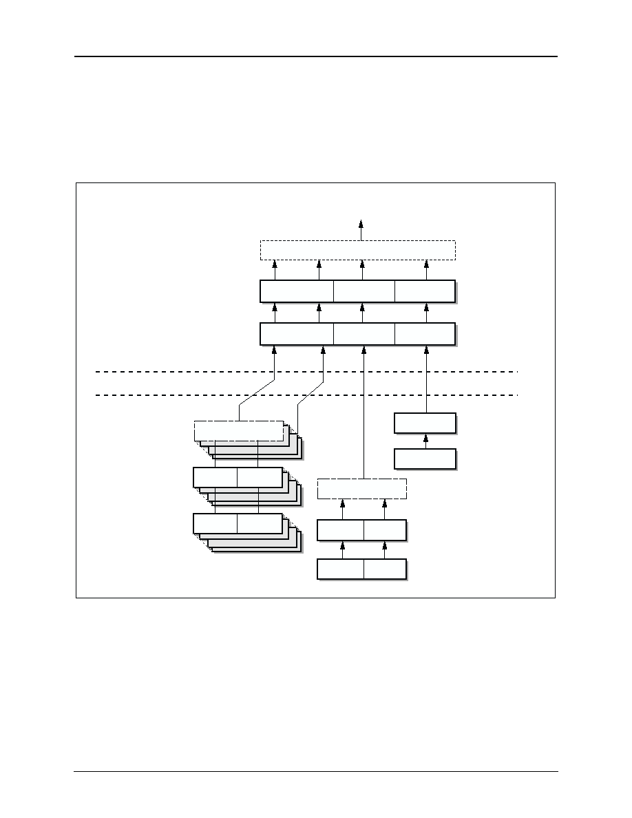
500238B
Mindspeed TechnologiesTM
8
-
165
Advance Information
CX29503 Data Sheet
Register Description
8.5.3
Interrupt Structures
The transmit interrupt structure is shown in
Figure 8-6
. The Level 1 status bits are the clear-on-read type. The
Level 3 interrupt status bits are not the clear-on-read type and are cleared when the related Level 1 status bits are
cleared.
Figure 8-6. SONET/SDH Interrupt Structure--Transmit Path
. . .
100702_043
OR
Level 1
OR
Transmit STS/SDH Mapper Block Interrupt
(see Figure 2-20)
. . .
Level 3 (30 Interrupts)
VT/VC 1≠28
Interrupt Enables
STS Path
Interrupt Enable
General
Interrupt Enable
VT/VC 1≠28
Interrupt Statuses
STS Path
Interrupt Status
General
Interrupt Status
Transmit Channel Interrupt
Enable [addr: 6008≠600B]
Transmit Channel Interrupt
Status [addr: 600C≠600F]
TxStartErr
EnTxStartErr
Transmit SI-Bus
Status [addr: 6001]
Transmit SI-Bus
Interrupt Enable
[addr: 6000]
Map3µF
Map3OF
. . .
EnMap1µF
EnMap1OF
Map1µF
Map1OF
1≠28
EnMap3µF EnMap3OF
OR
Transmit DS3/E3
Mapping FIFO Status
[addr: 623F]
Transmit DS3/E3
Mapping FIFO
Interrupt Enable
[addr: 6237]
VT#n Transmit
Mapping FIFO Interrupt
Enable [addr: 0x37]
VT#n Transmit
Mapping FIFO Interrupt
Status [addr: 0x3F]
Level 2 (not applicable)
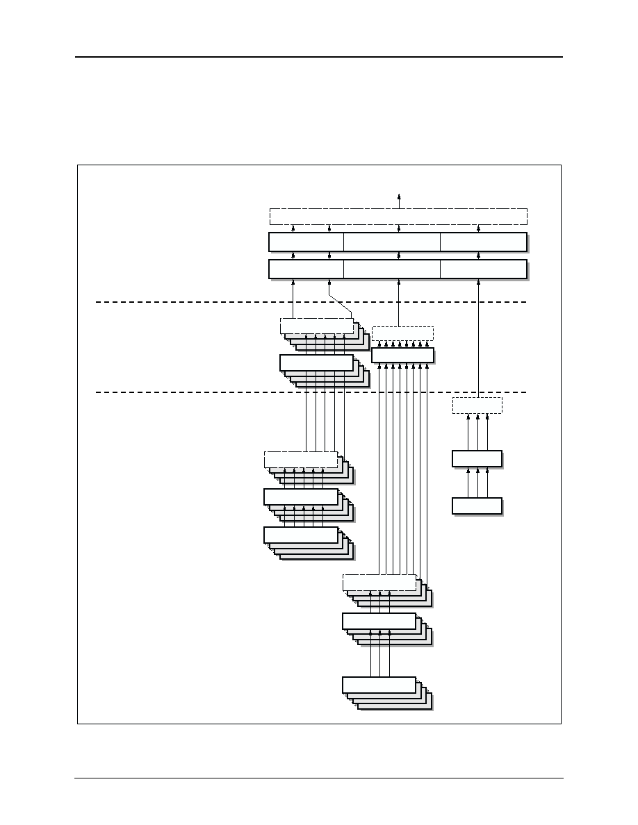
8-166
Mindspeed TechnologiesTM
500238B
Advance Information
Register Description
CX29503 Data Sheet
The receive interrupt structure is shown in
Figure 8-7
. The Level 1 status bits are the
clear-on-read type. The Level 2 interrupt source and Level 3 interrupt status bits are
not clear-on-read type and are cleared when the related Level 1 status bits are cleared.
Figure 8-7. SONET/SDH Interrupt Structure--Receive Path
. . .
Level 1
OR
Receive STS/SDH Mapper Block Interrupt
(see Figure 2-20)
. . .
Level 3 (30 Interrupts)
VT/VC 1≠28
Interrupt Enables
STS Path
Interrupt Enable
General
Interrupt Enable
VT/VC 1≠28
Interrupt Statuses
STS Path
Interrupt Status
General
Interrupt Status
Receive Channel Interrupt
Enable [addr: 6088≠608B]
Transmit Channel Interrupt
Status [addr: 608C≠608F]
Status Bits
Enable Bits
Receive SI-Bus
Status [addr: 6081]
Receive SI-Bus
IE [addr: 6080]
. . .
1≠28
Status Bits
OR
Receive STS
Path Interrupt
Source
[addr: 62B0]
Status Bits
OR
Enable Bits
Receive Path Start of Status IE 1 [addr: 62B3]
Receive Path Start of Status IE 2 [addr: 62B4]
Receive Path End of Status IE 1 [addr: 62B5]
Receive Path End of Status IE 2 [addr: 62B6]
Receive Path Event Status IE [addr: 62B7]
Receive Tributary Start of Status IE [addr: 62F3]
Receive Tributary End of Status IE [addr: 62F5]
Receive Tributary Event Status IE [addr: 62F7]
Receive Path Start of Status 1 [addr: 62BB]
Receive Path Start of Status 2 [addr: 62BC]
Receive Path End of Status 1 [addr: 62BD]
Receive Path End of Status 2 [addr: 62BE]
Receive Path Event Status [addr: 62BF]
Receive Tributary Start of Status [addr: 62FB]
Receive Tributary End of Status [addr: 62FD]
Receive Tributary Event Status [addr: 62FF]
VT#n Receive VT
Interrupt Source
[addr: 0xB0]
Level 2
Status Bits
OR
VT#n Receive VT Start of Status IE 1 [addr: 0xB3]
VT#n Receive VT Start of Status IE 2 [addr: 0xB4]
VT#n Receive VT End of Status IE 1 [addr: 0xB5]
VT#n Receive VT End of Status IE 2 [addr: 0xB6]
VT#n Receive VT Event Status IE [addr: 0xB7]
VT#n Receive VT Start of Status 1 [addr: 0xBB]
VT#n Receive VT Start of Status 2 [addr: 0xBC]
VT#n Receive VT End of Status 1 [addr: 0xBD]
VT#n Receive VT End of Status 2 [addr: 0xBE]
VT#n Receive VT Event Status [addr: 0xBF]
Status Bits
OR
Enable Bits
OR
100702_044

500238B
Mindspeed TechnologiesTM
8
-
167
Advance Information
CX29503 Data Sheet
Register Description
8.5.4
General Control and Status Registers
Table 8-54
provides a map of the General Control and Status registers.
Section 8.5.4.1
contains the register bit
descriptions.
Table 8-54. SONET/SDH General Control and Status Register <tableContinuation>(1 of 2)
Offset
(Hex)
Typ
e
Clear on
Read
Register Description
Value After Reset
(Hex or
Undefined)
SONET/SDH Top Level Transmitter Control
6000
R/
W
No
Transmit SI-Bus Interrupt Enable
0x00
6001
R
Yes
Transmit SI-Bus Status
0x00
6002≠6003
--
--
Undefined
--
6004
R/
W
No
BIP2 Error Pattern
0x00
6005
R/
W
No
Transmit Uproc Interface Fast Access Control
0x00
6006
---
--
Undefined
--
6007
R/
W
No
SI-Bus Transmit to Receive Loopback Control
0x00
SONET/SDH Level 3 Transmitter Interrupts
6008
R/
W
No
Transmit Channel Interrupt Enable (Channels 1≠8)
0x00
6009
R/
W
No
Transmit Channel Interrupt Enable (Channels 9≠16)
0x00
600A
R/
W
No
Transmit Channel Interrupt Enable (Channels 17≠24)
0x00
600B
R/
W
No
Transmit Channel Interrupt Enable (Channels 25≠28, STS, General)
0x00
600C
R
No
Transmit Channel Status (Channels 1≠8)
0x00
600D
R
No
Transmit Channel Status (Channels 9≠16)
0x00
600E
R
No
Transmit Channel Status (Channels 17≠24)
0x00
600F
R
No
Transmit Channel Status (Channels 25≠28, STS, General)
0x00
6010≠607F
--
--
Undefined
--
SONET/SDH Top Level Receiver Control
6080
R/
W
No
Receive SI-Bus Interrupt Enable
0x00
6081
R
Yes
Receive SI-Bus Status
0x00
6082
R
No
SI-Bus Phase Identifier
0x00
6083
--
--
Undefined
--

8-168
Mindspeed TechnologiesTM
500238B
Advance Information
Register Description
CX29503 Data Sheet
6084
R/
W
No
Status/Counter Latching Control
0x00
6085
R/
W
No
Receive Microprocessor Interface Fast Access Control
0x00
6086≠6087
--
--
Undefined
--
SONET/SDH Level 3 Receiver Interrupts
6088
R/
W
No
Receive Channel Interrupt Enable (Channels 1≠8)
0x00
6089
R/
W
No
Receive Channel Interrupt Enable (Channels 9≠16)
0x00
608A
R/
W
No
Receive Channel Interrupt Enable (Channels 17≠24)
0x00
608B
R/
W
No
Receive Channel Interrupt Enable (Channels 25≠28, STS, General)
0x00
608C
R
No
Receive Channel Status (Channels 1≠8)
0x00
608D
R
No
Receive Channel Status (Channels 9≠16)
0x00
608E
R
No
Receive Channel Status (Channels 17≠24)
0x00
608F
R
No
Receive Channel Status (Channels 25≠28, STS, General)
0x00
6090≠60FF
--
--
Undefined
--
Table 8-54. SONET/SDH General Control and Status Register <tableContinuation>(2 of 2)
Offset
(Hex)
Typ
e
Clear on
Read
Register Description
Value After Reset
(Hex or
Undefined)

500238B
Mindspeed TechnologiesTM
8
-
169
Advance Information
CX29503 Data Sheet
Register Description
8.5.4.1
SONET/SDH Top Level Transmitter Control
0x6000--Transmit SI-Bus Interrupt Enable
This interrupt register is at Level 1 in the SONET/SDH transmit interrupt hierarchy (see
Figure 8-6
). The
corresponding Level 3 interrupt is the Transmit General interrupt in the Transmit Channel Status register
[addr: 0FF].
Reset State
0x00
EnTxStartErr
Transmit Start Error Status Interrupt Enable (1 = enable)
0x6001--Transmit SI-Bus Status
This register is a clear-on-read-type.
Reset State
0x00
TxStartErr
Transmit Start Signal Changed Phase--This status shows that an event has occurred since the
register was last read.
0x6004--BIP2 Error Pattern (Used for Diagnostics)
Reset State
0x00
ErrPat[7:6]
Error Pattern--This pattern is used to insert errors in the BIP2 field. This error pattern is
inserted on the VT path or paths that have the BIP2ErrIns bit in the VT# Transmit Overhead
Control 1 register (see
Section 8.6.1
) enabled.
ErrPat[5:0]
Not used for the CX29503.
7
6
5
4
3
2
1
0
--
--
--
--
--
--
--
EnTxStartErr
7
6
5
4
3
2
1
0
--
--
--
--
--
--
v
TxStartErr
7
6
5
4
3
2
1
0
ErrPat[7]
ErrPat[6]
ErrPat[5]
ErrPat[4]
ErrPat[3]
ErrPat[2]
ErrPat[1]
ErrPat[0]

8-170
Mindspeed TechnologiesTM
500238B
Advance Information
Register Description
CX29503 Data Sheet
0x6005--Transmit Microprocessor Interface Fast Access Control
Reset State
0x00
FastAccess
Setting this bit removes the metastability guard and reduces access time by Ω clock cycle.
0x6007--SI-Bus Transmit to Receive Loopback Control
Reset State
0x00
TxRxLoopBk
Enable Internal SI-Bus loopback (SI-Bus transmit to SI-Bus receive)
7
6
5
4
3
2
1
0
--
--
--
--
v
--
--
FastAccess
7
6
5
4
3
2
1
0
--
--
--
--
--
--
--
TxRx LoopBk
500238B
Mindspeed TechnologiesTM
8
-
171
Advance Information
CX29503 Data Sheet
Register Description
8.5.4.2
SONET/SDH Level 3 Transmitter Interrupts
0x6008--Transmit Channel Interrupt Enable (Channels 1≠8)
Reset State
0x00
EnTxChInt1
Transmit Channel 1 (VT/VC #1) Interrupt Enable Bit (1 = enable)
EnTxChInt2
Transmit Channel 1 (VT/VC #2) Interrupt Enable Bit (1 = enable)
EnTxChInt3
Transmit Channel 1 (VT/VC #3) Interrupt Enable Bit (1 = enable)
EnTxChInt4
Transmit Channel 1 (VT/VC #4) Interrupt Enable Bit (1 = enable)
EnTxChInt5
Transmit Channel 1 (VT/VC #5) Interrupt Enable Bit (1 = enable)
EnTxChInt6
Transmit Channel 1 (VT/VC #6) Interrupt Enable Bit (1 = enable)
EnTxChInt7
Transmit Channel 1 (VT/VC #7) Interrupt Enable Bit (1 = enable)
EnTxChInt8
Transmit Channel 1 (VT/VC #8) Interrupt Enable Bit (1 = enable)
0x6009--Transmit Channel Interrupt Enable (Channels 9≠16)
Reset State
0x00
EnTxChInt9
Transmit Channel 1 (VT/VC #9) Interrupt Enable Bit (1 = enable)
EnTxChInt10
Transmit Channel 1 (VT/VC #10) Interrupt Enable Bit (1 = enable)
EnTxChInt11
Transmit Channel 1 (VT/VC #11) Interrupt Enable Bit (1 = enable)
EnTxChInt12
Transmit Channel 1 (VT/VC #12) Interrupt Enable Bit (1 = enable)
EnTxChInt13
Transmit Channel 1 (VT/VC #13) Interrupt Enable Bit (1 = enable)
EnTxChInt14
Transmit Channel 1 (VT/VC #14) Interrupt Enable Bit (1 = enable)
EnTxChInt15
Transmit Channel 1 (VT/VC #15) Interrupt Enable Bit (1 = enable)
EnTxChInt16
Transmit Channel 1 (VT/VC #16) Interrupt Enable Bit (1 = enable)
7
6
5
4
3
2
1
0
EnTx ChInt8
EnTx ChInt7
EnTx ChInt6
EnTx ChInt5
EnTx ChInt4
EnTx ChInt3
EnTx ChInt2
EnTx ChInt1
7
6
5
4
3
2
1
0
EnTx ChInt16
EnTx ChInt15
EnTx ChInt14
EnTx ChInt13
EnTx ChInt12
EnTx ChInt11
EnTx ChInt10
EnTx ChInt9

8-172
Mindspeed TechnologiesTM
500238B
Advance Information
Register Description
CX29503 Data Sheet
0x600A--Transmit Channel Interrupt Enable (Channels 17≠24)
Reset State
0x00
EnTxChInt17
Transmit Channel 1 (VT/VC #17) Interrupt Enable Bit (1 = enable)
EnTxChInt18
Transmit Channel 1 (VT/VC #18) Interrupt Enable Bit (1 = enable)
EnTxChInt19
Transmit Channel 1 (VT/VC #19) Interrupt Enable Bit (1 = enable)
EnTxChInt20
Transmit Channel 1 (VT/VC #20) Interrupt Enable Bit (1 = enable)
EnTxChInt21
Transmit Channel 1 (VT/VC #21) Interrupt Enable Bit (1 = enable)
EnTxChInt22
Transmit Channel 1 (VT/VC #22) Interrupt Enable Bit (1 = enable)
EnTxChInt23
Transmit Channel 1 (VT/VC #23) Interrupt Enable Bit (1 = enable)
EnTxChInt24
Transmit Channel 1 (VT/VC #24) Interrupt Enable Bit (1 = enable)
0x600B--Transmit Channel Interrupt Enable (Channels 17≠24, STS, General)
Reset State
0x00
EnTxChInt25
Transmit Channel 1 (VT/VC #25) Interrupt Enable Bit (1 = enable)
EnTxChInt26
Transmit Channel 1 (VT/VC #26) Interrupt Enable Bit (1 = enable)
EnTxChInt27
Transmit Channel 1 (VT/VC #27) Interrupt Enable Bit (1 = enable)
EnTxChInt28
Transmit Channel 1 (VT/VC #28) Interrupt Enable Bit (1 = enable)
EnTxIntSTS
Transmit STS Path Interrupt Enable Bit (1 = enable)
EnTxIntGen
Transmit General Interrupt Enable Bit (1 = enable)--This interrupt enables the pass-through
of any Level 1 interrupt that is enabled in the Transmit SI-Bus Interrupt enable [addr: 000]
7
6
5
4
3
2
1
0
EnTx ChInt24
EnTx ChInt23
EnTx ChInt22
EnTx ChInt21
EnTx ChInt20
EnTx ChInt19
EnTx ChInt18
EnTx ChInt17
7
6
5
4
3
2
1
0
EnTx IntGen
Reserved
Reserved
EnTx IntSTS
EnTx ChInt28
EnTx ChInt27
EnTx ChInt26
EnTx ChInt25

500238B
Mindspeed TechnologiesTM
8
-
173
Advance Information
CX29503 Data Sheet
Register Description
0x600C--Transmit Channel Status (Channels 1≠8)
Reset State
0x00
TxChInt1
Transmit Channel 1 (VT/VC #1) Interrupt Status
TxChInt2
Transmit Channel 1 (VT/VC #2) Interrupt Status
TxChInt3
Transmit Channel 1 (VT/VC #3) Interrupt Status
TxChInt4
Transmit Channel 1 (VT/VC #4) Interrupt Status
TxChInt5
Transmit Channel 1 (VT/VC #5) Interrupt Status
TxChInt6
Transmit Channel 1 (VT/VC #6) Interrupt Status
TxChInt7
Transmit Channel 1 (VT/VC #7) Interrupt Status
TxChInt8
Transmit Channel 1 (VT/VC #8) Interrupt Status
0x600D--Transmit Channel Status (Channels 9≠16)
Reset State
0x00
TxChInt9
Transmit Channel 1 (VT/VC #9) Interrupt Status
TxChInt10
Transmit Channel 1 (VT/VC #10) Interrupt Status
TxChInt11
Transmit Channel 1 (VT/VC #11) Interrupt Status
TxChInt12
Transmit Channel 1 (VT/VC #12) Interrupt Status
TxChInt13
Transmit Channel 1 (VT/VC #13) Interrupt Status
TxChInt14
Transmit Channel 1 (VT/VC #14) Interrupt Status
TxChInt15
Transmit Channel 1 (VT/VC #15) Interrupt Status
TxChInt16
Transmit Channel 1 (VT/VC #16) Interrupt Status
7
6
5
4
3
2
1
0
TxChInt8
TxChInt7
TxChInt6
TxChInt5
TxChInt4
TxChInt3
TxChInt2
TxChInt1
7
6
5
4
3
2
1
0
Tx ChInt16
Tx ChInt15
Tx ChInt14
Tx ChInt13
Tx ChInt12
Tx ChInt11
Tx ChInt10
Tx ChInt9

8-174
Mindspeed TechnologiesTM
500238B
Advance Information
Register Description
CX29503 Data Sheet
0x600E--Transmit Channel Status (Channels 17≠24)
Reset State
0x00
TxChInt17
Transmit Channel 1 (VT/VC #17) Interrupt Status
TxChInt18
Transmit Channel 1 (VT/VC #18) Interrupt Status
TxChInt19
Transmit Channel 1 (VT/VC #19) Interrupt Status
TxChInt20
Transmit Channel 1 (VT/VC #20) Interrupt Status
TxChInt21
Transmit Channel 1 (VT/VC #21) Interrupt Status
TxChInt22
Transmit Channel 1 (VT/VC #22) Interrupt Status
TxChInt23
Transmit Channel 1 (VT/VC #23) Interrupt Status
TxChInt24
Transmit Channel 1 (VT/VC #24) Interrupt Status
0x600F--Transmit Channel Status (Channels 17≠24, STS, General)
Reset State
0x00
TxChInt25
Transmit Channel 1 (VT/VC #25) Interrupt Status
TxChInt26
Transmit Channel 1 (VT/VC #26) Interrupt Status
TxChInt27
Transmit Channel 1 (VT/VC #27) Interrupt Status
TxChInt28
Transmit Channel 1 (VT/VC #28) Interrupt Status
TxIntSTS
Transmit STS Path Interrupt Status
TxIntGen
Transmit General Interrupt Status
7
6
5
4
3
2
1
0
Tx ChInt24
Tx ChInt23
Tx ChInt22
Tx ChInt21
Tx ChInt20
Tx ChInt19
Tx ChInt18
Tx ChInt17
7
6
5
4
3
2
1
0
TxIntGen
Reserved
Reserved
TxIntSTS
Tx ChInt28
Tx ChInt27
Tx ChInt26
Tx ChInt25

500238B
Mindspeed TechnologiesTM
8
-
175
Advance Information
CX29503 Data Sheet
Register Description
8.5.4.3
SONET/SDH Top Level Receiver Control
0x6080--Receive SI-Bus Interrupt Enable
This interrupt register is at Level 3 in the SONET interrupt hierarchy. The corresponding level 1 interrupt is the
Receive General Interrupt in the Transmit Channel Status register [addr: 08F].
Reset State
0x00
EnRxStartErr
Receive Start Error Interrupt Enable (1 = enable)
EnRxSyncErr
Receive Start Sync Error Interrupt Enable (1 = enable)
EnRxParErr
Receive Data Parity Error Interrupt Enable (1 = enable)
0x6081--Receive SI-Bus Status
Reset State
0x00
RxStartErr
Receive Start Signal, Changed Phase
RxSyncErr
Receive Start Signal Not Coincident with Valid A1 Byte
RxParErr
Parity Error Occurred on the Receive SI-Bus
0x6082--SI-Bus Phase Identifier
Reset State
0x00
SI-BusID[1:0]
SI-Bus Phase Identifier--This value identifies which channel corresponds to this mapper/
MUX slice in the device.
00 = channel 0
01 = channel 1
10 = channel 2
11 = undefined
7
6
5
4
3
2
1
0
--
--
--
--
--
EnRx ParErr
EnRx SyncErr
EnRx StartErr
7
6
5
4
3
2
1
0
--
--
--
--
--
RxParErr
RxSync Err
Rx StartErr
7
6
5
4
3
2
1
0
--
--
--
--
--
--
SI-BusID [1]
SI-BusID [0]

8-176
Mindspeed TechnologiesTM
500238B
Advance Information
Register Description
CX29503 Data Sheet
0x6084--Receive Status/Counter Latching Control
Reset State
0x00
EnErrLat
One-second latching is enabled for all Receive Error counters when set; otherwise, error count
information is updated continuously up to counter saturation.
EnStatLat
One-second latching is enabled for all Receive Status counters when set; otherwise, status
count information is updated continuously up to counter saturation.
BlkCnt
When set, BIP or REI errors received increments the respective error counter by 1 count for
each errored frame; otherwise, the actual number of BIP or REI errors received is added to the
respective error counter.
PerCap
All Overhead Receive Capture registers, except trace buffers, have a persistence capture where
the captured value changes only after 3 consecutive frames of a consistent value when set;
otherwise, the Overhead Capture registers contain the current values.
0x6085--Receive Microprocessor Interface Fast Access Control
Reset State
0x00
FastAccess
Setting this bit removes the metastability guard and reduces access time by Ω clock cycle.
7
6
5
4
3
2
1
0
--
--
--
--
PerCap
BlkCnt
EnStatLat
EnErrLat
7
6
5
4
3
2
1
0
--
--
--
--
--
--
--
FastAccess

500238B
Mindspeed TechnologiesTM
8
-
177
Advance Information
CX29503 Data Sheet
Register Description
8.5.4.4
SONET/SDH Level 3 Receiver Interrupts
0x6088--Receive Channel Interrupt Enable (Channels 1≠8)
These bits enable the pass-through of Level 2 interrupts reported in the VT #1≠#8 Receive VT Interrupt Source
registers (see
Section 8.6.2
).
Reset State
0x00
EnRxChInt1
Receive Channel 1 (VT #1) Interrupt Enable Bit
EnRxChInt2
Receive Channel 2 (VT #2) Interrupt Enable Bit
EnRxChInt3
Receive Channel 3 (VT #3) Interrupt Enable Bit
EnRxChInt4
Receive Channel 4 (VT #4) Interrupt Enable Bit
EnRxChInt5
Receive Channel 5 (VT #5) Interrupt Enable Bit
EnRxChInt6
Receive Channel 6 (VT #6) Interrupt Enable Bit
EnRxChInt7
Receive Channel 7 (VT #7) Interrupt Enable Bit
EnRxChInt8
Receive Channel 8 (VT #8) Interrupt Enable Bit
0x6089--Receive Channel Interrupt Enable (Channels 9≠16)
These bits enable the pass through of Level 2 interrupts reported in the VT #9≠#16 Receive VT Interrupt Source
registers (
Section 8.6.2
).
Reset State
0x00
EnRxChInt9
Receive Channel 9 (VT #9) Interrupt Enable Bit
EnRxChInt10
Receive Channel 10 (VT #10) Interrupt Enable Bit
EnRxChInt11
Receive Channel 11 (VT #11) Interrupt Enable Bit
EnRxChInt12
Receive Channel 12 (VT #12) Interrupt Enable Bit
EnRxChInt13
Receive Channel 13 (VT #13) Interrupt Enable Bit
EnRxChInt14
Receive Channel 14 (VT #14) Interrupt Enable Bit
EnRxChInt15
Receive Channel 15 (VT #15) Interrupt Enable Bit
EnRxChInt16
Receive Channel 16 (VT #16) Interrupt Enable Bit
7
6
5
4
3
2
1
0
EnRx ChInt8
EnRx ChInt7
EnRx ChInt6
EnRx ChInt5
EnRx ChInt4
EnRx ChInt3
EnRx ChInt2
EnRx ChInt1
7
6
5
4
3
2
1
0
EnRx ChInt16
EnRx ChInt15
EnRx ChInt14
EnRx ChInt13
EnRx ChInt12
EnRx ChInt11
EnRx ChInt10
EnRx ChInt9

8-178
Mindspeed TechnologiesTM
500238B
Advance Information
Register Description
CX29503 Data Sheet
0x608A--Receive Channel Interrupt Enable (Channels 17≠24)
These bits enable the pass-through of Level 2 interrupts reported in the VT #17≠#24 Receive VT Interrupt
Source registers (
Section 8.6.2
).
Reset State
0x00
EnRxChInt17
Receive Channel 17 (VT #17) Interrupt Enable Bit
EnRxChInt18
Receive Channel 18 (VT #18) Interrupt Enable Bit
EnRxChInt19
Receive Channel 19 (VT #19) Interrupt Enable Bit
EnRxChInt20
Receive Channel 20 (VT #20) Interrupt Enable Bit
EnRxChInt21
Receive Channel 21 (VT #21) Interrupt Enable Bit
EnRxChInt22
Receive Channel 22 (VT #22) Interrupt Enable Bit
EnRxChInt23
Receive Channel 23 (VT #23) Interrupt Enable Bit
EnRxChInt24
Receive Channel 24 (VT #24) Interrupt Enable Bit
0x608B--Receive Channel Interrupt Enable (Channels 25≠28, STS, General)
Bits 0≠4 enable the pass-through of Level 2 interrupts reported in the VT #25≠#28 Receive VT Interrupt Source
registers (
Section 8.6.2
).
Reset State
0x00
EnRxChInt25
Receive Channel 25 (VT #25) Interrupt Enable Bit
EnRxChInt26
Receive Channel 26 (VT #26) Interrupt Enable Bit
EnRxChInt27
Receive Channel 27 (VT #27) Interrupt Enable Bit
EnRxChInt28
Receive Channel 28 (VT #28) Interrupt Enable Bit
EnRxChIntSTS
Receive STS Path Interrupt Enable Bit--This interrupt enables the pass-through of any
Level 2 interrupt reported in the Receive STS Path Interrupt source [addr: 0x62B0].
EnRxChIntGen
Receive General Interrupt Enable Bit--This interrupt enables the pass-through of any Level 1
interrupt enabled in the Receive SI-Bus Interrupt enable [addr: 0x6080].
7
6
5
4
3
2
1
0
EnRx ChInt24
EnRx ChInt23
EnRx ChInt22
EnRx ChInt21
EnRx ChInt20
EnRx ChInt19
EnRx ChInt18
EnRx ChInt17
7
6
5
4
3
2
1
0
EnRxCh
IntGen
Reserved
Reserved
EnRxCh
IntSTS
EnRx ChInt28
EnRx ChInt27
EnRx ChInt26
EnRx ChInt25

500238B
Mindspeed TechnologiesTM
8
-
179
Advance Information
CX29503 Data Sheet
Register Description
0x608C--Receive Channel Status (Channels 1≠8)
Reset State
0x00
RxChInt1
Receive Channel 1 (VT #1) Interrupt Status Bit
RxChInt2
Receive Channel 2 (VT #2) Interrupt Status Bit
RxChInt3
Receive Channel 3 (VT #3) Interrupt Status Bit
RxChInt4
Receive Channel 4 (VT #4) Interrupt Status Bit
RxChInt5
Receive Channel 5 (VT #5) Interrupt Status Bit
RxChInt6
Receive Channel 6 (VT #6) Interrupt Status Bit
RxChInt7
Receive Channel 7 (VT #7) Interrupt Status Bit
RxChInt8
Receive Channel 8 (VT #8) Interrupt Status Bit
0x608D--Receive Channel Status (Channels 9≠16)
Reset State
0x00
RxChInt9
Receive Channel 9 (VT #9) Interrupt Status Bit
RxChInt10
Receive Channel 10 (VT #10) Interrupt Status Bit
RxChInt11
Receive Channel 11 (VT #11) Interrupt Status Bit
RxChInt12
Receive Channel 12 (VT #12) Interrupt Status Bit
RxChInt13
Receive Channel 13 (VT #13) Interrupt Status Bit
RxChInt14
Receive Channel 14 (VT #14) Interrupt Status Bit
RxChInt15
Receive Channel 15 (VT #15) Interrupt Status Bit
RxChInt16
Receive Channel 16 (VT #16) Interrupt Status Bit
7
6
5
4
3
2
1
0
RxChInt8
RxChInt7
RxChInt6
RxChInt5
RxChInt4
RxChInt3
RxChInt2
RxChInt1
7
6
5
4
3
2
1
0
Rx ChInt16
Rx ChInt15
Rx ChInt14
Rx ChInt13
Rx ChInt12
Rx ChInt11
Rx ChInt10
Rx ChInt9

8-180
Mindspeed TechnologiesTM
500238B
Advance Information
Register Description
CX29503 Data Sheet
0x608E--Receive Channel Status (Channels 17≠24)
Reset State
0x00
RxChInt17
Receive Channel 17 (VT #17) Interrupt Status Bit
RxChInt18
Receive Channel 18 (VT #18) Interrupt Status Bit
RxChInt19
Receive Channel 19 (VT #19) Interrupt Status Bit
RxChInt20
Receive Channel 20 (VT #20) Interrupt Status Bit
RxChInt21
Receive Channel 21 (VT #21) Interrupt Status Bit
RxChInt22
Receive Channel 22 (VT #22) Interrupt Status Bit
RxChInt23
Receive Channel 23 (VT #23) Interrupt Status Bit
RxChInt24
Receive Channel 24 (VT #24) Interrupt Status Bit
0x608F--Receive Channel Status (Channels 25≠28, STS, General)
Reset State
0x00
RxChInt25
Receive Channel 25 (VT #25) Interrupt Status Bit
RxChInt26
Receive Channel 26 (VT #26) Interrupt Status Bit
RxChInt27
Receive Channel 27 (VT #27) Interrupt Status Bit
RxChInt28
Receive Channel 28 (VT #28) Interrupt Status Bit
RxChIntSTS
Receive STS Path Interrupt Status Bit
RxChIntGen
Receive General Interrupt Status Bit
7
6
5
4
3
2
1
0
Rx ChInt24
Rx ChInt23
Rx ChInt22
Rx ChInt21
Rx ChInt20
Rx ChInt19
Rx ChInt18
Rx ChInt17
7
6
5
4
3
2
1
0
RxCh IntGen
Reserved
Reserved
RxCh IntSTS
Rx ChInt28
Rx ChInt27
Rx ChInt26
Rx ChInt25

500238B
Mindspeed TechnologiesTM
8
-
181
Advance Information
CX29503 Data Sheet
Register Description
8.5.5
STS-1 Framer Section/Line Control/Status
Table 8-55
provides a map of the Control and Status registers in the Section/Line Layer section of this STS-1
memory map. Following the table are the register bit descriptions.
0x6100--Transmit Transport Overhead Byte Insertion Control (TXTOHINS)
Reset State
0x00
InsLDCC
Line DCC bytes contain values from the TSB, otherwise, Line DCC bytes contain 0x00
InsSDCC
Section DCC bytes contain values from the TSB, otherwise, Section DCC bytes contain 0x00
0x6180--Receive Transport Overhead Byte Drop Control (RXTOHDROP)
Reset State
0x00
DrpLDCC
Line DCC bytes are passed to the TSB
DrpSDCC
Section DCC bytes are passed to the TSB
Table 8-55. STS-1 Framer Section/Line Control/Status Registers
Offset (Hex)
Name
Type
Clear on
Read
Register Description
Value After
Reset
(Hex or
Undefined)
6100
TXTOHINS
R/W
No
Transmit Transport Overhead Byte Insertion
Control
0x00
6101≠617F
--
--
--
Reserved
--
6180
RXTOHDROP
R/W
No
Receive Transport Overhead Byte Drop
Control
0x00
6181≠61FF
--
--
--
Reserved
--
7
6
5
4
3
2
1
0
--
--
--
--
--
--
InsSDCC
InsLDCC
7
6
5
4
3
2
1
0
--
--
--
--
--
--
DrpSDCC
DrpLDCC

8-182
Mindspeed TechnologiesTM
500238B
Advance Information
Register Description
CX29503 Data Sheet
8.5.6
STS-1/AU≠4/AU-3 and TU-3 Path Control/Status Registers
Table 8-56
provides a map of the Control and Status registers in the Path Layer section of the STS-1/AU-4/AU-
3 and TU-3 memory map. Following the table are the register bit descriptions.
This register block monitors the first stage of demultiplexing/multiplexing at the STS-1/AU-4/AU-3 level. In
addition, this register block monitors the second stage of demultiplexing/multiplexing that occurs in SDH when
the TUG-3 bit is set in the Level 3 Mapping Control register [addr: 0x6380]. This second stage monitors the
TU-3 processing in the SDH multiplexing path AU-4
VC-4
TUG-3
TU-3
VC-3.
Table 8-56. STS-1/AU-4/AU-3 and TU-3 Path Control/Status Registers <tableContinuation>(1 of 4)
Offset (Hex))
Typ
e
Clear on Read
Register Description
Value After Reset
(Hex or Undefined)
Transmit STS-1/AU-4/AU-3 Overhead (
Section 8.5.6.1
)
6200
R/W
No
Transmit Path Overhead Control
0x00
6201
R/W
--
Reserved
--
6202
R/W
No
Transmit Path Overhead Byte Insertion Control
0x00
6203≠6205
R/W
--
Reserved
--
6206
--
--
Undefined
--
6207
R/W
No
Transmit Path F2 Overhead Byte
0x00
6208
--
--
Undefined
--
6209
R/W
No
Transmit Path Z3/F3 Overhead Byte
0x00
620A
R/W
No
Transmit Path Z4/K3 Overhead Byte
0x00
620B
R/W
No
Transmit Path Z5/N1 Overhead Byte
0x00
620C≠620D
--
--
Undefined
--
Transmit DS3/E3 Mapper FIFO (
Section 8.5.6.2
)
620E
R/W
No
Transmit DS3/E3 Mapping FIFO Minimum Level
0x00
620F
R/W
No
Transmit DS3/E3 Mapping FIFO Reset
0x00
6210≠6236
--
--
Undefined
--
6237
R/W
No
Transmit DS3/E3 Mapping FIFO Interrupt Enable
0x00
6238≠623E
--
--
Undefined
--
623F
R
Yes
Transmit DS3/E3 Mapping FIFO Status
0x00
Transmit TU-3 Overhead (
Section 8.5.6.3
)
6240
R/W
No
Transmit TU-3 Overhead Control
0x00
6241
R/W
--
Reserved
--
6242
R/W
No
Transmit TU-3 Overhead Byte Insertion Control
0x00
6243≠6245
R/W
--
Reserved
--
6246
--
--
Undefined
--
6247
R/W
No
Transmit TU-3 F2 Overhead Byte
0x00
6248
--
--
Undefined
--

500238B
Mindspeed TechnologiesTM
8
-
183
Advance Information
CX29503 Data Sheet
Register Description
6249
R/W
No
Transmit TU-3 Z3/F3 Overhead Byte
0x00
624A
R/W
No
Transmit TU-3 Z4/K3 Overhead Byte
0x00
624B
R/W
No
Transmit TU-3 Z5/N1 Overhead Byte
0x00
Receive STS-1/AU-4/AU-3 Overhead (
Section 8.5.6.4
)
624C≠6280
--
--
Undefined
--
6281
R/W
--
Reserved
--
6282
R/W
No
Receive Path Overhead Byte Drop Control
0x00
6283≠6284
R/W
--
Reserved
--
6285≠628B
R
--
Reserved
--
Receive DS3/E3 Demapper FIFO (
Section 8.5.6.5
)
628C≠628D
--
--
Undefined
--
628E
R/W
No
Receive DS3/E3 Demapping FIFO Minimum Level
0x00
628F
R/W
No
Receive DS3/E3 Demap FIFO Reset
0x00
6290≠6293
R
--
Reserved
--
STS-1/AU-4/AU-3 Pointer Processing (
Section 8.5.6.6
)
6294
R
No
Receive STS-1/AU-4/AU-3 Pointer Value
(8 LSBits)
0x00
6295
R
Partial
Receive STS-1/AU-4/AU-3 Pointer Status
0x00
6296
R
Yes,
if EnStatLat = 0
Receive STS-1/AU-4/AU-3 Pointer Increment Counter LSB
0x00
6297
R
Yes,
if EnStatLat = 0
Receive STS-1/AU-4/AU-3 Pointer Increment Counter MSB
0x00
6298
R
Yes,
if EnStatLat = 0
Receive STS-1/AU-4/AU-3 Pointer Decrement Counter LSB
0x00
6299
R
Yes,
if EnStatLat = 0
Receive STS-1/AU-4/AU-3 Pointer Decrement Counter MSB
0x00
629A≠62AF
--
--
Undefined
--
STS Path Level 2 Interrupts (
Section 8.5.6.7
)
62B0
R
No
Receive STS Path Interrupt Source
0x00
62B1≠62B2
--
--
Undefined
--
STS Path Level 1 Interrupts--STS-1/AU-4/AU-3 (
Section 8.5.6.8
)
62B3
R/W
No
Receive Path Start of Status Interrupt Enable 1
0x00
62B4
R/W
No
Receive Path Start of Status Interrupt Enable 2
0x00
62B5
R/W
No
Receive Path End of Status Interrupt Enable 1
0x00
62B6
R/W
No
Receive Path End of Status Interrupt Enable 2
0x00
Table 8-56. STS-1/AU-4/AU-3 and TU-3 Path Control/Status Registers <tableContinuation>(2 of 4)
Offset (Hex))
Typ
e
Clear on Read
Register Description
Value After Reset
(Hex or Undefined)

8-184
Mindspeed TechnologiesTM
500238B
Advance Information
Register Description
CX29503 Data Sheet
62B7
R/W
No
Receive Path Event Status Interrupt Enable
0x00
62B8
--
--
Undefined
--
62B9
R
No
Receive Path Current Status 1
0x00
62BA
R
No
Receive Path Current Status 2
0x00
62BB
R
Yes
Receive Path Start of Status 1
0x00
62BC
R
Yes
Receive Path Start of Status 2
0x00
62BD
R
Yes
Receive Path End of Status 1
0x00
62BE
R
Yes
Receive Path End of Status 2
0x00
62BF
R
Yes
Receive Path Event Status
0x00
62C0
--
--
Undefined
--
Receive TU-3 Overhead (
Section 8.5.6.9
)
62C1
R/W
--
Reserved
--
62C2
R/W
No
Receive TU-3 Overhead Byte Drop Control
0x00
62C3≠62C4
R/W
--
Reserved
--
62C5≠62CB
R
--
Reserved
--
62CC≠62CF
--
--
Undefined
--
62D0≠62D3
--
--
Reserved
--
Receive TU-3 Pointer Processing (
Section 8.5.6.10
)
62D4
R
No
Receive TU-3 Pointer Value (8 LSBits)
0x00
62D5
R
Partial
Receive TU-3 Pointer Status
0x00
62D6
R
Yes,
if EnStatLat = 0
Receive TU-3 Pointer Increment Counter LSB
0x00
62D7
R
Yes,
if EnStatLat = 0
Receive TU-3 Pointer Increment Counter MSB
0x00
62D8
R
Yes,
if EnStatLat = 0
Receive TU-3 Pointer Decrement Counter LSB
0x00
62D9
R
Yes,
if EnStatLat = 0
Receive TU-3 Pointer Decrement Counter MSB
0x00
62DA≠62F2
--
--
Undefined
--
STS Path Level 1 Interrupts --TU-3 (
Section 8.5.6.11
)
62F3
--
--
Receive TU-3 Start of Status Interrupt Enable
--
62F4
--
--
Undefined
--
62F5
--
--
Receive TU-3 End of Status Interrupt Enable
--
62F6
--
--
Undefined
--
62F7
R/W
--
Receive TU-3 Event Status Interrupt Enable
0x00
Table 8-56. STS-1/AU-4/AU-3 and TU-3 Path Control/Status Registers <tableContinuation>(3 of 4)
Offset (Hex))
Typ
e
Clear on Read
Register Description
Value After Reset
(Hex or Undefined)

500238B
Mindspeed TechnologiesTM
8
-
185
Advance Information
CX29503 Data Sheet
Register Description
62F8
--
--
Undefined
--
62F9
R
--
Receive TU-3 Current Status
0x00
62FA
--
--
Undefined
--
62FB
R
Yes
Receive TU-3 Start of Status
0x00
62FC
--
--
Undefined
--
62FD
R
Yes
Receive TU-3 End of Status
0x00
62FE
---
--
Undefined
--
62FF
R
Yes
Receive TU-3 Event Status
0x00
Table 8-56. STS-1/AU-4/AU-3 and TU-3 Path Control/Status Registers <tableContinuation>(4 of 4)
Offset (Hex))
Typ
e
Clear on Read
Register Description
Value After Reset
(Hex or Undefined)

8-186
Mindspeed TechnologiesTM
500238B
Advance Information
Register Description
CX29503 Data Sheet
8.5.6.1 Transmit
STS-1/AU≠4/AU-3 Overhead
0x6200--Transmit Path Overhead Control
Reset State
0x00
InsAIS-P
Generates Path AIS when set.
0x6202--Transmit Path Overhead Byte Insertion Control (TXPOHINS)
Reset State
0x00
InsN1
Data link nibble of the Z5/N1 byte contains values from the TSB with the Incoming Error
Count (IEC) nibble from the TXN1 register [addr: 0x620B]; otherwise, the complete Z5/N1
value is inserted from TXN1 register [addr: 0x620B].
InsK3
The Z4/K3 byte contain values from the TSB; otherwise, the Z4/K3 value is inserted from
TXK3 register [addr: 0x620A].
InsF3
The Z3/F3 byte contain values from the TSB; otherwise the Z3/F3 value is inserted from TXF3
register [addr: 0x6209].
InsF2
The F2 byte contain values from the TSB; otherwise, the F2 value is inserted from TXF2
register [addr: 0x6207].
0x6207--Transmit Path F2 Overhead Byte (TXF2)
Reset State
0x00
TxF2[7:0]
Transmit value for the F2 byte. This byte is transmitted if the InsF2 bit in TXPOHINS
[addr: 6202] is cleared.
7
6
5
4
3
2
1
0
Reserved
Reserved
Reserved
Reserved
Reserved
Reserved
Reserved
InsAIS-P
7
6
5
4
3
2
1
0
--
--
--
--
InsF2
InsF3
InsK3
InsN1
7
6
5
4
3
2
1
0
TxF2 [7]
TxF2 [6]
TxF2 [5]
TxF2 [4]
TxF2 [3]
TxF2 [2]
TxF2 [1]
TxF2 [0]

500238B
Mindspeed TechnologiesTM
8
-
187
Advance Information
CX29503 Data Sheet
Register Description
0x6209--Transmit Path Z3/F3 Overhead Byte (TXF3)
Reset State
0x00
TxF3 [7:0]
Transmit value for the Z3/F3 byte. This byte is transmitted if the InsF3 bit in TXPOHINS
[addr: 6202] is cleared.
0x620A--Transmit Path Z4/K3 Overhead Byte (TXK3)
Reset State
0x00
TxK3 [7:0]
Transmit value for the Z4/K3 byte. This byte is transmitted if the InsK3 bit in TXPOHINS
[addr: 6202] is cleared.
0x620B--Transmit Path Z5/N1 Overhead Byte (TXN1)
Reset State
0x00
TxN1 [7:0]
Transmit value for the Z5/N1 byte. The upper nibble, TxN1[7]≠TxN1[4], is the IEC nibble.
The lower nibble is the DL nibble. The IEC nibble is transmitted if the InsN1 bit in
TXPOHINS [addr: 6202] is set; otherwise, the complete byte is transmitted.
7
6
5
4
3
2
1
0
TxF3 [7]
TxF3 [6]
TxF3 [5]
TxF3 [4]
TxF3 [3]
TxF3 [2]
TxF3 [1]
TxF3 [0]
7
6
5
4
3
2
1
0
TxK3 [7]
TxK3 [6]
TxK3 [5]
TxK3 [4]
TxK3 [3]
TxK3 [2]
TxK3 [1]
TxK3 [0]
7
6
5
4
3
2
1
0
TxN1 [7]
TxN1 [6]
TxN1 [5]
TxN1 [4]
TxN1 [3]
TxN1 [2]
TxN1 [1]
TxN1 [0]

8-188
Mindspeed TechnologiesTM
500238B
Advance Information
Register Description
CX29503 Data Sheet
8.5.6.2
Transmit DS3/E3 Mapping FIFO
0x620E--Transmit DS3/E3 Mapping FIFO Minimum Level (TXL3MAPMIN)
Reset State
0x00
Map3ML[6:0]
DS3/E3 Mapping FIFO Minimum Level for stuffing rate selection
0x620F--Transmit DS3/E3 Mapping FIFO Reset (TXL3MAPRST)
Reset State
0x00
Map3Reset
DS3/E3 Mapping FIFO Reset
Map3HWRstDis
DS3/E3 Mapping FIFO HW Reset Disable
0x6237--Transmit DS3/E3 Mapping FIFO Interrupt Enable
Reset State
0x00
EnMap3OF
DS3/E3 Mapping FIFO Overflow Interrupt Enable
EnMap3UF
DS3/E3 Mapping FIFO Underflow Interrupt Enable
0x623F--Transmit DS3/E3 Mapping FIFO Status, Diagnostic Only
This register is a clear-on-read type.
Reset State
0x00
Map3OF
DS3/E3 Mapping FIFO Overflow Status
Map3UF
DS3/E3 Mapping FIFO Underflow Status
7
6
5
4
3
2
1
0
--
Map3ML[6]
Map3ML[5]
Map3ML[4]
Map3ML[3]
Map3ML[2]
Map3ML[1]
Map3ML[0]
7
6
5
4
3
2
1
0
--
--
--
--
--
--
Map3HWRstDi
s
Map3Reset
7
6
5
4
3
2
1
0
--
--
--
--
--
--
EnMap3UF
EnMap3OF
7
6
5
4
3
2
1
0
--
--
--
--
--
--
Map3UF
Map3OF

500238B
Mindspeed TechnologiesTM
8
-
189
Advance Information
CX29503 Data Sheet
Register Description
8.5.6.3
Transmit TU-3 Overhead
0x6240--Transmit TU-3 Overhead Control
Reset State
0x00
InsTrAIS-P
Generates the TU-3 Path AIS when set.
0x6242--Transmit TU-3 Overhead Byte Insertion Control (TXTU3INS)
Reset State
0x00
InsTrN1
Data link nibble of the TU-3 Z5/N1 byte contains values from the TSB with the IEC nibble
from the TU-3 TXTRN1 register [addr: 624B]; otherwise, the complete TU-3 N1/Z5 value is
inserted from the TU-3 TXTRN1 register [addr: 624B].
InsTrK3
TU-3 Z4/K3 byte contains values from the TSB; otherwise, the TU-3 Z4/K3 value is inserted
from the TU-3 TXTRK3 register [addr: 24A].
InsTrF3
TU-3 Z3/F3 byte contains values from the TSB; otherwise, the TU-3 Z3/F3 value is inserted
from the TU-3 TXTRF3 register [addr: 249].
InsTrF2
TU-3 F2 byte contains values from the TSB; otherwise, the TU-3 F2 value is inserted from the
TU-3 TXTRF2 register [addr: 247].
0x6247--Transmit TU-3 F2 Overhead Byte (TXTRF2)
Reset State
0x00
TxTrF2[7:0]
Transmit value for the TU-3 F2 byte. This byte is transmitted if the InsTrF2 bit in TXTU3INS
[addr: 6242] is cleared.
7
6
5
4
3
0x62
1
0
InsTrAIS-P
Reserved
Reserved
Reserved
Reserved
Reserved
Reserved
Reserved
7
6
5
4
3
2
1
0
--
--
--
--
InsTrF2
InsTrF3
InsTrK3
InsTrN1
7
6
5
4
3
2
1
0
TxTrF2 [7]
TxTrF2 [6]
TxTrF2 [5]
TxTrF2 [4]
TxTrF2 [3]
TxTrF2 [2]
TxTrF2 [1]
TxTrF2 [0]

8-190
Mindspeed TechnologiesTM
500238B
Advance Information
Register Description
CX29503 Data Sheet
0x6249--Transmit TU-3 Z3/F3 Overhead Byte (TXTRF3)
Reset State
0x00
TxTrF3 [7:0]
Transmit value for the TU-3 Z3/F3 byte. This byte is transmitted if the InsTrF3 bit in
TXTU3INS [addr: 6242] is cleared.
0x624A--Transmit TU-3 Z4/K3 Overhead Byte (TXTRK3)
Reset State
0x00
TxTrK3 [7:0]
Transmit value for the TU-3 Z4/K3 byte. This byte is transmitted if the InsTrK3 bit in
TXTU3INS [addr: 6242] is cleared.
0x624B--Transmit TU-3 Z5/N1 Overhead Byte (TXTRN1)
Reset State
0x00
TxTrN1 [7:0]
Transmit value for the TU-3 Z5/N1 byte. The upper nibble, TxTrN1[7]≠TxTrN1[4], is the IEC.
The lower nibble is the DL nibble. The IEC nibble is transmitted if the InsTrN1 bit in
TXTU3INS [addr: 6242] is set; otherwise, the complete byte is transmitted.
7
6
5
4
3
2
1
0
TxTrF3 [7]
TxTrF3 [6]
TxTrF3 [5]
TxTrF3 [4]
TxTrF3 [3]
TxTrF3 [2]
TxTrF3 [1]
TxTrF3 [0]
7
6
5
4
3
2
1
0
TxTrK3 [7]
TxTrK3 [6]
TxTrK3 [5]
TxTrK3 [4]
TxTrK3 [3]
TxTrK3 [2]
TxTrK3 [1]
TxTrK3 [0]
7
6
5
4
3
2
1
0
TxTrN1 [7]
TxTrN1 [6]
TxTrN1 [5]
TxTrN1 [4]
TxTrN1 [3]
TxTrN1 [2]
TxTrN1 [1]
TxTrN1 [0]

500238B
Mindspeed TechnologiesTM
8
-
191
Advance Information
CX29503 Data Sheet
Register Description
8.5.6.4
Receive STS-1/AU-4/AU-3 Overhead
0x6282--Receive Path Overhead Byte Drop Control
Reset State
0x00
DrpN1
Data link portion of the Z5/N1byte is passed to the TSB
DrpK3
Z4/K3 byte is passed to the TSB
DrpF3
Z3/F3 byte is passed to the TSB
DrpF2
F2 byte is passed to the TSB
8.5.6.5
Receive DS3/E3 Demapping FIFO
0x628E--Receive DS3/E3 Demapping FIFO Minimum Level (RXL3DEMMIN)
Reset State
0x00
Dem3ML[7:0]
DS3/E3 Demapping FIFO Minimum Level for stuffing rate selection
0x628F--Receive DS3/E3 Demap FIFO Reset (RXL3DEMRST)
Reset State
0x00
Dem3Reset
DS3/E3 Demapping FIFO Reset
Smth3Reset
DS3/E3 Smoothing FIFO Reset
Smth3HWRstDis
DS3/E3 Smoothing FIFO HW Reset Disable
7
6
5
4
3
2
1
0
--
--
--
--
DrpF2
DrpF3
DrpK3
DrpN1
7
6
5
4
3
2
1
0
Dem3ML[7]
Dem3ML[6]
Dem3ML[5]
Dem3ML[4]
Dem3ML[3]
Dem3ML[2]
Dem3ML[1]
Dem3ML[0]
7
6
5
4
3
2
1
0
--
--
--
--
--
Smth3HWRst
Dis
Smth3Reset
Dem3Reset

8-192
Mindspeed TechnologiesTM
500238B
Advance Information
Register Description
CX29503 Data Sheet
8.5.6.6
STS-1/AU-4/AU-3 Pointer Processing
0x6294--Receive STS-1/AU-4/AU-3 Pointer Value (8 LSBits)
Reset State
0x00
Pntr [7:0]
STS-1/AU-4/AU-3 pointer value 8 LSBits--Current State
0x6295--Receive STS-1/AU-4/AU-3 Pointer Status
Reset State
0x00
Pntr [9:8]
STS-1/AU-4/AU-3 pointer value 2 MSBits--Current State
SS[1:0]
STS-1/AU-4/AU-3 pointer value SS bits--Current State
This bit does not require that the SDHSSEn bit [addr: 3080] be set.
Decr
STS-1/AU-4/AU-3 pointer decrement operation occurred. This bit is a clear-on-read type.
Incr
STS-1/AU-4/AU-3 pointer increment operation occurred. This bit is a clear-on-read type.
NewPntr
New STS-1/AU-4/AU-3 pointer without NDF was received. This bit is a clear-on-read type.
NDF
STS-1/AU-4/AU-3 pointer NDF was received. This bit is a clear-on-read type.
0x6296--Receive STS-1/AU-4/AU-3 Pointer Increment Counter LSB
This register is a clear-on-read type if EnStatLat in STATMODE [addr: 6084] equals 0.
Reset State
0x00
PJCnt [7:0]
STS-1/AU-4/AU-3 positive pointer justification counter LSB.
7
6
5
4
3
2
1
0
Pntr [7]
Pntr [6]
Pntr [5]
Pntr [4]
Pntr [3]
Pntr [2]
Pntr [1]
Pntr [0]
7
6
5
4
3
2
1
0
NDF
NewPntr
Incr
Decr
SS[1]
SS[0]
Pntr[9]
Pntr[8]
7
6
5
4
3
2
1
0
PJCnt [7]
PJCnt [6]
PJCnt [5]
PJCnt [4]
PJCnt [3]
PJCnt [2]
PJCnt [1]
PJCnt [0]

500238B
Mindspeed TechnologiesTM
8
-
193
Advance Information
CX29503 Data Sheet
Register Description
0x6297--Receive STS-1/AU-4/AU-3 Pointer Increment Counter MSB
This register is a clear-on-read type if EnStatLat in STATMODE [addr: 6084] equals 0.
Reset State
0x00
PJCnt [15:8]
STS-1/AU-4/AU-3 positive pointer justification counter MSB.
0x6298--Receive STS-1/AU-4/AU-3 Pointer Decrement Counter LSB
This register is a clear-on-read type if EnStatLat in STATMODE [addr: 6084] equals 0.
Reset State
0x00
NJCnt [7:0]
STS-1/AU-4/AU-3 negative pointer justification counter LSB.
0x6299--Receive STS-1/AU-4/AU-3 Pointer Decrement Counter MSB
This register is a clear-on-read type if EnStatLat in STATMODE [addr: 6084] equals 0.
Reset State
0x00
NJCnt [15:8]
STS-1/AU-4/AU-3 negative pointer justification counter MSB.
7
6
5
4
3
2
1
0
PJCnt [15]
PJCnt [14]
PJCnt [13]
PJCnt [12]
PJCnt [11]
PJCnt [10]
PJCnt [9]
PJCnt [8]
7
6
5
4
3
2
1
0
NJCnt [7]
NJCnt [6]
NJCnt [5]
NJCnt [4]
NJCnt [3]
NJCnt [2]
NJCnt [1]
NJCnt [0]
7
6
5
4
3
2
1
0
NJCnt [15]
NJCnt [14]
NJCnt [13]
NJCnt [12]
NJCnt [11]
NJCnt [10]
NJCnt [9]
NJCnt [8]

8-194
Mindspeed TechnologiesTM
500238B
Advance Information
Register Description
CX29503 Data Sheet
8.5.6.7
STS Path Level 2 Interrupts
0x62B0--Receive STS Path Interrupt Source
Reset State
0x00
IntRxPth
STS path interrupt due to various status indicators in the RXPEVSTAT register [addr: 2BF]
IntRxEdPth2
STS path interrupt due to various status indicators in the RXPESTAT2 register [addr: 2BE]
IntRxEdPth1
STS path interrupt due to various status indicators in the RXPESTAT1 register [addr: 2BD]
IntRxStPth2
STS path interrupt due to various status indicators in the RXPSSTAT2 register [addr: 2BC]
IntRxStPth1
STS path interrupt due to various status indicators in the RXPSSTAT1 register [addr: 2BB]
IntRxTrPth
STS path interrupt due to various status indicators in the RXTEVSTAT register [addr: 2FF]
IntRxEdTrPth
STS path interrupt due to various status indicators in the RXTESTAT register [addr: 2FD]
IntRxStTrPth
STS path interrupt due to various status indicators in the RXTSSTAT register [addr: 2FB]
7
6
5
4
3
2
1
0
IntRxStTrPth
IntRxEdTrPth
IntRxTrPth
IntRxStPth1
IntRxStPth2
IntRxEdPth1
IntRxEdPth2
IntRxPth

500238B
Mindspeed TechnologiesTM
8
-
195
Advance Information
CX29503 Data Sheet
Register Description
8.5.6.8
STS Path Level 1 Interrupts--STS-1/AU≠4/AU-3
0x62B3--Receive Path Start of Status Interrupt Enable 1
Reset State
0x00
EnStLOP-P
Start of LOP-P Condition Interrupt is enabled when set
EnStAIS-P
Start of AIS-P Condition Interrupt is enabled when set
0x62B4--Receive Path Start of Status Interrupt Enable 2
Reset State
0x00
EnStH4LOMF
Start of H4LOMF Condition Interrupt is enabled when set
0x62B5--Receive Path End of Status Interrupt Enable 1
Reset State
0x00
EnEdLOP-P
End of LOP-P Condition Interrupt is enabled when set
EnEdAIS-P
End of AIS-P Condition Interrupt is enabled when set
0x62B6--Receive Path End of Status Interrupt Enable 2
Reset State
0x00
EnEdH4LOMF
End of H4LOMF Condition Interrupt is enabled when set
7
6
5
4
3
2
1
0
Reserved
Reserved
Reserved
Reserved
Reserved
Reserved
EnStAIS-P
EnStLOP-P
7
6
5
4
3
2
1
0
--
--
--
--
--
--
Reserved
EnStH4LOMF
7
6
5
4
3
2
1
0
Reserved
Reserved
Reserved
Reserved
Reserved
Reserved
EnEdAIS-P
EnEdLOP-P
7
6
5
4
3
2
1
0
--
--
--
--
--
--
Reserved
EnEdH4LOMF

8-196
Mindspeed TechnologiesTM
500238B
Advance Information
Register Description
CX29503 Data Sheet
0x62B7--Receive Path Event Status Interrupt Enable
Reset State
0x00
EnSmth3OF
DS3/E3 Smoothing FIFO Overflow Interrupt is enabled when set (used for Diagnostics)
EnSmth3UF
DS3/E3 Smoothing FIFO Underflow Interrupt is enabled when set (used for Diagnostics)
EnNwPtr
STS-1/AU-4/AU-3 New Pointer Interrupt Enable is enabled when set
0x62B9--Receive Path Current Status 1
Reset State
0x00
LOP-P
LOP-P Condition Exists--Current State
AIS-P
AIS-P Condition Exists--Current State
0x62BA--Receive Path Current Status 2
Reset State
0x00
H4LOMF
Invalid H4 multiframe indicator exists--Current State
0x62BB--Receive Path Start of Status 1 (RXPSSTAT1)
Reset State
0x00
StLOP-P
Start of LOP-P condition
StAIS-P
Start of AIS-P condition
7
6
5
4
3
2
1
0
--
--
Reserved
Reserved
Reserved
EnNwPtr
EnSmth3UF
EnSmth3OF
7
6
5
4
3
2
1
0
Reserved
Reserved
Reserved
Reserved
Reserved
Reserved
AIS-P
LOP-P
7
6
5
4
3
2
1
0
--
--
--
--
--
--
Reserved
H4LOMF-P
7
6
5
4
3
2
1
0
Reserved
Reserved
Reserved
Reserved
Reserved
Reserved
StAIS-P
StLOP-P

500238B
Mindspeed TechnologiesTM
8
-
197
Advance Information
CX29503 Data Sheet
Register Description
0x62BC--Receive Path Start of Status 2 (RXPSSTAT2)
Reset State
0x00
StH4LOMF
Start of Invalid H4 Multiframe Indicator
0x62BD--Receive Path End of Status 1 (RXPESTAT1)
Reset State
0x00
EdLOP-P
End of LOP-P Condition
EdAIS-P
End of AIS-P Condition
0x62BE--Receive Path End of Status 2 (RXPESTAT2)
Reset State
0x00
EdH4LOMF
End of Invalid H4 Multiframe Indicator
0x62BF--Receive Path Event Status (RXPEVSTAT)
Reset State
0x00
Smth3OF
DS3/E3 Smoothing FIFO Overflow occurred
Smth3UF
DS3/E3 Smoothing FIFO Underflow occurred
NwPtr
STS-1/AU-4/AU-3 New Pointer with or without NDF occurred
7
6
5
4
3
2
1
0
--
--
--
--
--
--
Reserved
StH4LOMF
7
6
5
4
3
2
1
0
Reserved
Reserved
Reserved
Reserved
Reserved
Reserved
EdAIS-P
EdLOP-P
7
6
5
4
3
2
1
0
--
--
--
--
--
--
Reserved
EdH4LOMF
7
6
5
4
3
2
1
0
--
--
Reserved
Reserved
Reserved
NwPtr
Smth3UF
Smth3OF

8-198
Mindspeed TechnologiesTM
500238B
Advance Information
Register Description
CX29503 Data Sheet
8.5.6.9
Receive TU-3 Overhead
0x62C2--Receive TU-3 Overhead Byte Drop Control
Reset State
0x00
DrpTrN1
Data link portion of the TU-3 Z5/N1 byte is passed to the TSB.
DrpTrK3
TU-3 Z4/K3 byte is passed to the TSB.
DrpTrF3
TU-3 Z3/F3 byte is passed to the TSB.
DrpTrF2
TU-3 F2 byte is passed to the TSB.
7
6
5
4
3
2
1
0
--
--
--
--
DrpTrF2
DrTrpF3
DrpTrK3
DrpTrN1

500238B
Mindspeed TechnologiesTM
8
-
199
Advance Information
CX29503 Data Sheet
Register Description
8.5.6.10
Receive TU-3 Pointer Processing
0x62D4--Receive TU-3 Pointer Value (8 LSBits)
Reset State
0x00
Pntr TU3 [7:0]
TU-3 Pointer Value is 8 LSBits--Current State
0x62D5--Receive TU-3 Pointer Status
Reset State
0x00
Pntr TU3 [9:8]
TU-3 pointer value 2 MSBits--Current State
SS TU3[1:0]
TU-3 pointer value SS bits--Current State
Decr TU3
TU-3 pointer decrement operation occurred. This bit is a clear-on-read type.
Incr TU3
TU-3 pointer increment operation occurred. This bit is a clear-on-read type.
NewPntr TU3
TU-3 pointer without NDF was received. This bit is a clear-on-read type.
NDF TU3
TU-3 pointer NDF was received. This bit is a clear-on-read type.
0x62D6--Receive TU-3 Pointer Increment Counter LSB
This register is a clear-on-read type if EnStatLat in STATMODE [addr: 6084] equals 0.
Reset State
0x00
PJCnt TU3 [7:0]
TU-3 positive pointer justification counter LSB.
7
6
5
4
3
2
1
0
Pntr TU3 [7]
Pntr TU3 [6]
Pntr TU3 [5]
Pntr TU3 [4]
Pntr TU3 [3]
Pntr TU3 [2]
Pntr TU3 [1]
Pntr TU3 [0]
7
6
5
4
3
2
1
0
NDF TU3
NewPntr TU3
Incr TU3
Decr TU3
SS TU3[1]
SS TU3[0]
Pntr TU3 [9]
Pntr TU3 [8]
7
6
5
4
3
2
1
0
PJCnt TU3 [7] PJCnt TU3 [6] PJCnt TU3 [5] PJCnt TU3 [4] PJCnt TU3 [3] PJCnt TU3 [2] PJCnt TU3 [1] PJCnt TU3 [0]

8-200
Mindspeed TechnologiesTM
500238B
Advance Information
Register Description
CX29503 Data Sheet
0x62D7--Receive TU-3 Pointer Increment Counter MSB
This register is clear-on-read type if EnStatLat in STATMODE [addr: 6084] equals 0.
Reset State
0x00
PJCnt TU3 [15:8]
TU-3 positive pointer justification counter MSB.
0x62D8--Receive TU-3 Pointer Decrement Counter LSB
This register is a clear-on-read type if EnStatLat in STATMODE [addr: 6084] equals 0.
Reset State
0x00
NJCnt TU3 [7:0]
TU-3 positive pointer justification counter LSB.
0x62D9--Receive TU-3 Pointer Decrement Counter MSB
This register is a clear-on-read type if EnStatLat in STATMODE [addr: 6084] equals 0.
Reset State
0x00
NJCnt TU3 [15:8]
TU-3 positive pointer justification counter MSB.
7
6
5
4
3
2
1
0
PJCnt TU3
[15]
PJCnt TU3
[14]
PJCnt TU3
[13]
PJCnt TU3
[12]
PJCnt TU3
[11]
PJCnt TU3
[10]
PJCnt TU3 [9] PJCnt TU3 [8]
7
6
5
4
3
2
1
0
NJCnt TU3 [7] NJCnt TU3 [6] NJCnt TU3 [5] NJCnt TU3 [4] NJCnt TU3 [3] NJCnt TU3 [2] NJCnt TU3 [1] NJCnt TU3 [0]
7
6
5
4
3
2
1
0
NJCnt TU3
[15]
NJCnt TU3
[14]
NJCnt TU3
[13]
NJCnt TU3
[12]
NJCnt TU3
[11]
NJCnt TU3
[10]
NJCnt TU3 [9] NJCnt TU3 [8]

500238B
Mindspeed TechnologiesTM
8
-
201
Advance Information
CX29503 Data Sheet
Register Description
8.5.6.11
STS Path Level 1 Interrupts--TU-3
0x62F3--Receive TU-3 Start of Status Interrupt Enable
Reset State
0x00
EnStTrLOP-P
Start of TU-3 LOP-P Condition Interrupt is enabled when set
EnStTrAIS-P
Start of TU-3 AIS-P Condition Interrupt is enabled when set
0x62F5--Receive TU-3 End of Status Interrupt Enable
Reset State
0x00
EnEdTrLOP-P
End of TU-3 LOP-P Condition Interrupt is enabled when set
EnEdTrAIS-P
End of TU-3 AIS-P Condition Interrupt is enabled when set
0x62F7--Receive TU-3 Event Status Interrupt Enable
Reset State
0x00
EnTrNwPtrTU3
TU-3 New Pointer Interrupt Enable is enabled when set
0x62F9--Receive TU-3 Current Status
Reset State
0x00
TrLOP-P
TU-3 LOP-P Condition Exists--Current State
TrAIS-P
TU-3 AIS-P Condition Exists--Current State
7
6
5
4
3
2
1
0
Reserved
Reserved
Reserved
Reserved
Reserved
Reserved
EnStTrAIS-P
EnStTrLOP-P
7
6
5
4
3
2
1
0
Reserved
Reserved
Reserved
Reserved
Reserved
Reserved
EnEdTrAIS-P
EnEdTrLOP-P
7
6
5
4
3
2
1
0
--
--
--
--
Reserved
Reserved
Reserved
EnTrNwPtrTU3
7
6
5
4
3
2
1
0
Reserved
Reserved
Reserved
Reserved
Reserved
Reserved
TrAIS-P
TrLOP-P

8-202
Mindspeed TechnologiesTM
500238B
Advance Information
Register Description
CX29503 Data Sheet
0x62FB--Receive TU-3 Start of Status (RXTSSTAT)
Reset State
0x00
StTrLOP-P
Start of TU-3 LOP-P Condition
StTrAIS-P
Start of TU-3 AIS-P Condition
0x62FD--Receive TU-3 End of Status (RXTESTAT)
Reset State
0x00
EdTrLOP-P
End of TU-3 LOP-P Condition
EdTrAIS-P
End of TU-3 AIS-P Condition
0x62FF--Receive TU-3 Event Status (RXTEVSTAT)
Reset State
0x00
TrNwPtrTU3
TU-3 New Pointer with or without NDF occurred.
7
6
5
4
3
2
1
0
Reserved
Reserved
Reserved
Reserved
Reserved
Reserved
StTrAIS-P
StTrLOP-P
7
6
5
4
3
2
1
0
Reserved
Reserved
Reserved
Reserved
Reserved
Reserved
EdTrAIS-P
EdTrLOP-P
7
6
5
4
3
2
1
0
--
--
--
--
Reserved
Reserved
Reserved
TrNwPtrTU3

500238B
Mindspeed TechnologiesTM
8
-
203
Advance Information
CX29503 Data Sheet
Register Description
8.5.7
Mapping Control/Status Registers
Table 8-57
lists the Control and Status registers in the Tributary Mapping section of the memory map.
Following the table are the register bit descriptions.
0x6380--Level 3 Mapping Control
Reset State
0x00
L3Map[1:0]
Level 3 Mapping control--Controls the data path interface to the SI-Bus interface. If the
TUG3 bit (bit 2) is set, then the selected mapping is TUG-3; otherwise, it is STS-1/AU-3.
The L3Map[1:0] (see
Figure 8-8
) controls MUXes in the transmit data path and conceptual
switches in the receive data path. For simplicity,
Figure 8-8
does not show the data paths for
overhead data. See
Figure 2-2
for the top level view of the interfaces shown in
Figure 8-8
.
00 = unchannelized STS-1/AU-3 or TUG-3.
01 = tributary mapping via STS-1/AU-3 or TUG-3. This bit enables the tributary path.
The specific tributary data path (PDH or clear channel) is controlled by the
ClearCh1, ClearCh2, ClearCh3, and ClearCh4 bits in the Group n Mapping
Control registers [addr: 0x6388 to 0x638E].
10 = DS3 mapping via STS-1/AU-3 or TUG-3.
11 = E3 mapping via STS-1/AU-3 or TUG-3.
TUG3
TUG-3 mapping when set, otherwise STS-1/AU-3 mapping.
SDHSSEn
Discerns SS bits in AU-4/AU-3 SDH pointer interpretation and generation when set.
Table 8-57. Mapping Control/Status Registers
Offset (Hex)
Acronym
Type
Clear on
Read
Register Description
Value After Reset
(Hex or Undefined)
6300≠6307F
--
--
--
Undefined
--
6380
LVL3CFG
R/W
No
Level 3 Mapping Control
0x00
6381≠6387
--
--
--
Undefined
--
6388
GRPCFG1
R/W
No
Group 1 Mapping Control
0x00
6389
GRPCFG2
R/W
No
Group 2 Mapping Control
0x00
638A
GRPCFG3
R/W
No
Group 3 Mapping Control
0x00
638B
GRPCFG4
R/W
No
Group 4 Mapping Control
0x00
638C
GRPCFG5
R/W
No
Group 5 Mapping Control
0x00
638D
GRPCFG6
R/W
No
Group 6 Mapping Control
0x00
638E
GRPCFG7
R/W
No
Group 7 Mapping Control
0x00
638≠63FF
--
--
--
Undefined
--
7
6
5
4
3
2
1
0
--
--
--
--
SDHSSEn
TUG3
L3Map[1]
L3Map[0]
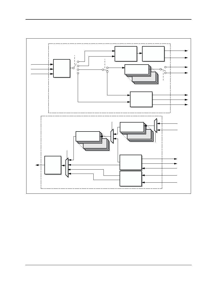
8-204
Mindspeed TechnologiesTM
500238B
Advance Information
Register Description
CX29503 Data Sheet
Figure 8-8. SONET Data Path Control
VT Overhead
Insertion (x 28)
Transmitter
DS1/E1 Mapping
Function (x 28)
DS1 Clock
and Data
E1 Clock
and Data
Receiver
SI-Bus
Interface
Rx STS-3 Data
Rx STS-3 Par
Rx Start
DS1 Clock
and Data
STS-1
Overhead
Insertion
Time Slot Bus
Interface
Control
Address
Data
DS3/E3
Demapping
Function
DS1/E1
Demapping
Function (x 28)
DS3/E3
Smoothing
Function
DS3/E3 Data
(Smoothed)
DS3/E3
Clock
DS3/E3
Mapping
Function
DS3/E3
Data
DS3/E3
Clock
Time Slot Bus
Interface
Control
Address
Data
L3Map[1:0]
Unchannelized STS-1/AU-3 or TUG-3
DS3
E3
Tributary
Clear Channel
(Not Supported)
PDH
ClearCh1≠4
GrpType
GrpType
E1 Clock
and Data
L3Map[1:0]
ClearCh1≠4
Unchannelized STS-1/AU-3 or TUG-3
Tributary
Clear Channel
(Not Nupported)
PDH
DS3
E3
100702_045

500238B
Mindspeed TechnologiesTM
8
-
205
Advance Information
CX29503 Data Sheet
Register Description
0x6388, 0x6389, 0x638A, 0x638B, 0x638C, 0x638D, and 0x638E--Group n Mapping
Control
Reset State
0x00
Only one description is provided for the Group n Mapping Control registers because the 7 registers have
identical bit definitions. The register offsets for the 7 registers are given in
Table 8-58
.
The settings in these registers are applicable only when L3Map[1:0] = 01 in the Level 3 Mapping Control
register [addr: 0x6380].
Each of the 7 VT/VC groups can be configured to be either VT1.5/VC-11 or VT2/VC-12. Within a VT/VC
group, each VT/VC can be configured to be PDH (DS1/E1)-mapped or clear channel-mapped.
These bits control MUXes in the receive data path and conceptual switches in the transmit data path
(see
Figure 8-8
).
ClearCh1
Group's VT#1 mapping control:
0 = PDH mapped (DS1/E1)
1 = Clear Channel mapped (not supported)
ClearCh2
Group's VT#2 mapping control:
0 = PDH mapped (DS1/E1)
1 = Clear Channel mapped (not supported)
ClearCh3
Group's VT#3 mapping control:
0 = PDH mapped (DS1/E1)
1 = Clear Channel mapped (not supported)
ClearCh4
Group's VT#4 mapping control:
0 = PDH mapped (DS1/E1)
1 = Clear Channel mapped (not supported)
GrpType
Group's mapping type:
0 = VC-11/VT1.5 mapped (DS1)
1 = VC-12/VT2 mapped (E1)
Table 8-58. Register Offsets--Group n Mapping Control
Offset (Hex)
Acronym
Register Description
VT #
DS1 #
0x6388
GRPCFG1
Group 1 Mapping Control
1≠4
1, 8, 15, 22
0x6389
GRPCFG2
Group 2 Mapping Control
5≠8
2, 9, 16, 23
0x638A
GRPCFG3
Group 3 Mapping Control
9≠12
3, 10, 17, 24
0x638B
GRPCFG4
Group 4 Mapping Control
13≠16
4, 11, 18, 25
0x638C
GRPCFG5
Group 5 Mapping Control
17≠20
5, 12, 19, 26
0x638D
GRPCFG6
Group 6 Mapping Control
21≠24
6, 13, 20, 27
0x638E
GRPCFG7
Group 7 Mapping Control
25≠28
7, 14, 21, 28
7
6
5
4
3
2
1
0
Reserved
--
--
GrpType
ClearCh4
ClearCh3
ClearCh2
ClearCh1

8-206
Mindspeed TechnologiesTM
500238B
Advance Information
Register Description
CX29503 Data Sheet
8.6
VT/VC Mapper Control and Status
Table 8-59
provides a map of the Control and Status registers in the Virtual Tributary section of the memory
map. Following the table are the register bit descriptions. The "n" in the register names refers to VT/VC
groups 1≠28.
Table 8-59. Tributary Control/Status Registers <tableContinuation>(1 of 2)
Offset (Hex)
Typ
e
Clear on Read
Register Description
Value After Reset
(Hex)
Transmit Tributary Processing
00
R/W
No
VT#n Transmit Overhead Control 1
0x00
01
R/W
No
VT#n Transmit Overhead Control 2
0x00
02
R/W
No
VT#n Transmit Signal Label Control
0x01
03
R/W
No
VT#n Transmit J2 Trace Circular Buffer Address
0x00
04
R/W
No
VT#n Transmit J2 Trace Circular Buffer Data
0x00
05
R/W
No
VT#n Transmit Z6/N2 Overhead Byte
0x00
06
R/W
No
VT#n Transmit Z7/K4 Overhead Byte
0x00
07≠0D
--
--
Undefined
0x00
0E
R/W
No
VT#n Transmit Mapping FIFO Minimum Level
0x00
0F
R/W
No
VT#n Transmit Mapping FIFO Reset
0x00
10≠1F
--
--
Undefined
0x00
20≠2F
--
--
Undefined
0x00
30≠36
--
--
Undefined
0x00
37
R/W
No
VT#n Transmit Mapping FIFO Interrupt Enable
0x00
38≠3E
--
--
Undefined
0x00
3F
R
Yes
VT#n Transmit Mapping FIFO Status
0x00
40 4F
--
--
Undefined
0x00
50≠5F
--
--
Undefined
0x00
60≠6F
--
--
Undefined
0x00
70≠7F
--
--
Undefined
0x00
Receive Tributary Processing
80
R/W
No
VT#n Receive Control
0x00
81
--
--
Undefined
0x00
82
R
No
VT#n Receive Signal Label Status
0x00
83
R/W
No
VT#n Receive J2 Trace Circular Buffer Address
0x00
84
R/W
No
VT#n Receive J2 Trace Circular Buffer Data
0x00
85
R
No
VT#n Receive Z6/N2 Overhead Status
0x00
86
R
No
VT#n Receive Z7/K4 Overhead Status
0x00

500238B
Mindspeed TechnologiesTM
8
-
207
Advance Information
CX29503 Data Sheet
Register Description
87≠8F
--
--
Undefined
0x00
90
R
Yes, if EnErrLat = 0
VT#n BIP2 Error Counter LSB
0x00
91
R
Yes, if EnErrLat = 0
VT#n BIP2 Error Counter MSB
0x00
92
R
Yes, if EnErrLat = 0
VT#n REI Error Counter LSB
0x00
93
R
Yes, if EnErrLat = 0
VT#n REI Error Counter MSB
0x00
94
R
No
VT#n Receive Pointer Value (8 LSBits)
0x00
95
R
Partial
VT#n Receive Pointer Status
0x00
96
R
Yes,
if EnStatLat = 0
VT#n Receive Pointer Increment Counter LSB
0x00
97
R
Yes,
if EnStatLat = 0
VT#n Receive Pointer Increment Counter MSB
0x00
98
R
Yes,
if EnStatLat = 0
VT#n Receive Pointer Decrement Counter LSB
0x00
99
R
Yes,
if EnStatLat = 0
VT#n Receive Pointer Decrement Counter MSB
0x00
9A≠9F
--
--
Undefined
0x00
A0≠AF
--
--
Undefined
0x00
B0
R
No
VT#n Receive VT Interrupt Source
0x00
B1≠B2
--
--
Undefined
0x00
B3
R/W
No
VT#n Receive VT Start of Status Interrupt Enable 1
0x00
B4
R/W
No
VT#n Receive VT Start of Status Interrupt Enable 2
0x00
B5
R/W
No
VT#n Receive VT End of Status Interrupt Enable 1
0x00
B6
R/W
No
VT#n Receive VT End of Status Interrupt Enable 2
0x00
B7
R/W
No
VT#n Receive VT Event Status Interrupt Enable
0x00
B8
--
--
Undefined
0x00
B9
R
No
VT#n Receive VT Current Status 1
0x00
BA
R
No
VT#n Receive VT Current Status 2
0x00
BB
R
Yes
VT#n Receive VT Start of Status 1
0x00
BC
R
Yes
VT#n Receive VT Start of Status 2
0x00
BD
R
Yes
VT#n Receive VT End of Status 1
0x00
BE
R
Yes
VT#n Receive VT End of Status 2
0x00
BF
R
Yes
VT#n Receive VT Event Status
0x00
C0≠CF
--
--
Undefined
0x00
D0≠DF
--
--
Undefined
0x00
E0≠EF
--
--
Undefined
0x00
F0≠FF
--
--
Undefined
0x00
Table 8-59. Tributary Control/Status Registers <tableContinuation>(2 of 2)
Offset (Hex)
Typ
e
Clear on Read
Register Description
Value After Reset
(Hex)
8-208
Mindspeed TechnologiesTM
500238B
Advance Information
Register Description
CX29503 Data Sheet
8.6.1
Transmit Tributary Processing
0x00--VT#n Transmit Overhead Control 1 (TXVTCTL1)
Reset State
0x00
InsAIS-V
When set, manually generates AIS-V in the transmit direction. This bit is for diagnostic
purposes.
InsRDI-V
This bit is inserted in the RDI-V field of the V5 byte if DisAutoRDI-V is set.
DisAutoRDI-V
When set, the value from bit 1 is inserted in the RDI-V field of the V5 byte and the values
from VT Transmit Z7/K4 Overhead Byte register (bits 3:1) are inserted in the ERDI-V field in
the Z7 byte when set; otherwise, ERDI-V codes are automatically inserted
TrigRDI-V
This bit is set based on an SONET-based or SDH-based application as listed in
Table 8-60
.
When RDIVMode (bit 4) is cleared, PLM-V is a trigger for ERDI-V in SONET; it is not a
trigger in SDH. When RDIVMode (bit 4) is set, UNEQ-V is a trigger for 1 bit RDI-V in SDH;
it is not a trigger in SONET.
RDIVMode
Automatic RDI-V generation is 1-bit RDI-V when set, Enhanced RDI-V otherwise.
InsRFI-V
The value inserted in the RFI-V field of the V5 byte.
DisAutoREI-V
Inserts 0 for the REI-V value when set; otherwise, REI-V codes are automatically inserted in
the V5 byte upon reception of BIP2 errors.
EnVTTr
Inserts VT Trace Message when set, otherwise the J2 byte contains 0x00. This bit should only
be set after the VT Trace Message is fully configured.
7
6
5
4
3
2
1
0
EnVTTr
DisAutoREI-V
InsRFI-V
RDIVMode
TrigRDI-V
DisAutoRDI-V
InsRDI-V
InsAIS-V
Table 8-60. Effect of TrigRDI-V and RDIVMode on Trigger-Initiated Actions
Mode
TrigRDI-V
RDIVMode
Trigger
Action
SONET
0
0
PLM-V
ERDI-V generated
--
0
1
UNEQ-V
No action
SDH
1
0
PLM-V
No action
--
1
1
UNEQ-V
1 bit, RDI-V generated

500238B
Mindspeed TechnologiesTM
8
-
209
Advance Information
CX29503 Data Sheet
Register Description
0x01--VT#n Transmit Overhead Control 2 (TXVTCTL2)
Reset State
0x00
DisBIP2
When set, the VT BIP-2 value contains 0x00, otherwise the BIP2 field in the V5 byte contains
the results of the VT BIP2 calculation.
BIP2ErrIns
When set, bits[7:6] of the Error Pattern Control register (See
Section 8.5.4.1
) are XORed with
the normal BIP2 value as determined by bit 0 when set; otherwise, the BIP2 field in the V5
byte is not errored.
InsK4
When set, bits 4≠7 in the VT Z7/K4 byte contain the values from the TSB; otherwise, bits 4≠7
are inserted from the TXK4 register [addr: 0x06].
0x02--VT#n Transmit Signal Label Control (TXVTLAB)
Reset State
0x01
TxVTLab [2:0]
Signal Label field of the V5 overhead byte. Default value indicates equipped VTs with
nonspecific payloads.
0x03--VT#n Transmit J2 Trace Circular Buffer Address (TXJ2ADD)
Reset State
0x00
TxJ2[3:0]
Transmit VT trace circular buffer. This register is the read/write location for access into a 16-
byte circular buffer used for VT trace messages inserted into the J2 byte.
0x04--VT#n Transmit J2 Trace Circular Buffer Data (TXJ2DAT)
Reset State
0x00
TxJ2[7:0]
Transmit VT trace circular buffer. This register is the read/write location for access into a 16-
byte circular buffer used for VT trace messages inserted into the J2 byte.
7
6
5
4
3
2
1
0
--
--
--
--
--
InsK4
BIP2 ErrIns
DisBIP2
7
6
5
4
3
2
1
0
--
--
--
--
--
TxVTLab [2]
TxVTLab [1]
TxVTLab [0]
7
6
5
4
3
2
1
0
--
--
--
--
TxJ2[3]
TxJ2[2]
TxJ2[1]
TxJ2[0]
7
6
5
4
3
2
1
0
TxJ2[7]
TxJ2[6]
TxJ2[5]
TxJ2[4]
TxJ2[3]
TxJ2[2]
TxJ2[1]
TxJ2[0]

8-210
Mindspeed TechnologiesTM
500238B
Advance Information
Register Description
CX29503 Data Sheet
0x05--VT#n Transmit Z6/N2 Overhead Byte (TXN2)
Reset State
0x00
TxN2[7:0]
Transmit value for Z6/N2 byte
0x06--VT#n Transmit Z7/K4 Overhead Byte (TXK4)
Reset State
0x00
TxK4[7:0]
Transmit value for Z7/K4 byte.
∑ Bit 0 is always inserted in the transmitted Z7/K4 byte.
∑ Bits 1≠3 are inserted into bits 1≠3 of the Z7/K4 byte when DisAutoRDI-V in
TXVTCTL1 [addr: 0x00] is set.
∑ Bits 4≠7 are inserted into bits 4≠7 of the Z7/K4 byte when InsK4 in TXVTCTL2
[addr: 0x02] is clear.
0x0E--VT#n Transmit Mapping FIFO Minimum Level (TXL1MAPMIN)
Reset State
0x00
Map1ML[6:0]
DS1/E1 Mapping FIFO Minimum Level for stuffing rate selection
0x0F--VT#n Transmit Mapping FIFO Reset (TXL1MAPRST)
Reset State
0x00
Map1Reset
DS1/E1 Mapping FIFO Reset
Map1HWRstDis
DS1/E1 Mapping FIFO HW Reset Disable
7
6
5
4
3
2
1
0
TxN2[7]
TxN2[6]
TxN2[5]
TxN2[4]
TxN2[3]
TxN2[2]
TxN2[1]
TxN2[0]
7
6
5
4
3
2
1
0
TxK4[7]
TxK4[6]
TxK4[5]
TxK4[4]
TxK4[3]
TxK4[2]
TxK4[1]
TxK4[0]
7
6
5
4
3
2
1
0
--
Map1ML[6]
Map1ML[5]
Map1ML[4]
Map1ML[3]
Map1ML[2]
Map1ML[1]
Map1ML[0]
7
6
5
4
3
2
1
0
--
--
--
--
--
--
Map1HWRstDi
s
Map1Reset

500238B
Mindspeed TechnologiesTM
8
-
211
Advance Information
CX29503 Data Sheet
Register Description
0x37--VT#n Transmit Mapping FIFO Interrupt Enable (TXL1MAPINTEN)
Reset State
0x00
EnMap1OF
Transmit Mapping FIFO Overflow Interrupt Enable
EnMap1UF
Transmit Mapping FIFO Underflow Interrupt Enable
0x3F--VT#n Transmit Mapping FIFO Status (TXL1MAPINTEN), Diagnostic Only
This register is a clear-on-read type.
Reset State
0x00
Map1OF
Transmit Mapping FIFO Overflow status
Map1UF
Transmit Mapping FIFO Underflow status
7
6
5
4
3
2
1
0
--
--
--
--
--
--
EnMap1UF
EnMap1OF
7
6
5
4
3
2
1
0
--
--
--
--
--
--
Map1UF
Map1OF

8-212
Mindspeed TechnologiesTM
500238B
Advance Information
Register Description
CX29503 Data Sheet
8.6.2
Receive Tributary Processing
0x80--VT#n Receive Control (RXVTCTL)
Reset State
0x00
ProvSL-V[2:0]
Provisioned VT signal label value, which is compared to the received VT signal label to
determine UNEQ-V and PLM-V error conditions.
Unused
This bit is implemented but not defined.
DrpK4
The K4 byte is passed to the TSB.
0x82--VT#n Receive Signal Label Status (RXVTLAB)
Reset State
0x00
RxVTLab [2:0]
The Signal Label field of the V5 byte--Current State
0x83--VT#n Receive J2 Trace Circular Buffer Address (RXJ2ADD
Reset State
0x00
RxJ2 [3:0]
Receive VT trace circular buffer. This register is the read location for access into a 16-byte
circular buffer used for VT trace messages received in the J2 byte.
0x84--VT#n Receive J2 Trace Circular Buffer Data (RXJ2DAT)
Reset State
0x00
RxJ2 [7:0]
Receive VT trace circular buffer. This register is the read location for access into a 16-byte
circular buffer used for VT trace messages received in the J2 byte.
7
6
5
4
3
2
1
0
--
--
--
DrpK4
Unused
ProvSL-V[2]
ProvSL-V[1]
ProvSL-V[0]
7
6
5
4
3
2
1
0
--
--
--
--
--
RxVTLab [2]
RxVTLab [1]
RxVTLab [0]
7
6
5
4
3
2
1
0
--
--
--
--
RxJ2 [3]
RxJ2 [2]
RxJ2 [1]
RxJ2 [0]
7
6
5
4
3
2
1
0
RxJ2 [7]
RxJ2 [6]
RxJ2 [5]
RxJ2 [4]
RxJ2 [3]
RxJ2 [2]
RxJ2 [1]
RxJ2 [0]

500238B
Mindspeed TechnologiesTM
8
-
213
Advance Information
CX29503 Data Sheet
Register Description
0x85--VT#n Receive Z6/N2 Overhead Status (RXN2)
Reset State
0x00
RxN2 [7:0]
Receive value for Z6/N2 byte
0x86--VT#n Receive Z7/K4 Overhead Status (RXK4)
Reset State
0x00
RxK4 [7:0]
Receive value for Z7/K4 byte
0x90--VT#n BIP2 Error Counter LSB (BIP2CNTL)
This register is a clear-on-read type if EnErrLat in STATMODE [addr: 6084] equals 0.
Reset State
0x00
BIP2Cnt [7:0]
BIP2 Error Counter LSB
0x91--VT#n BIP2 Error Counter MSB (BIP2CNTH)
This register is a clear-on-read type if EnErrLat in STATMODE [addr: 6084] equals 0.
Reset State
0x00
BIP2Cnt [15:8]
BIP2 Error Counter MSB
7
6
5
4
3
2
1
0
RxN2 [7]
RxN2 [6]
RxN2 [5]
RxN2 [4]
RxN2 [3]
RxN2 [2]
RxN2 [1]
RxN2 [0]
7
6
5
4
3
2
1
0
RxK4 [7]
RxK4 [6]
RxK4 [5]
RxK4 [4]
RxK4 [3]
RxK4 [2]
RxK4 [1]
RxK4 [0]
7
6
5
4
3
2
1
0
BIP2Cnt [7]
BIP2Cnt [6]
BIP2Cnt [5]
BIP2Cnt [4]
BIP2Cnt [3]
BIP2Cnt [2]
BIP2Cnt [1]
BIP2Cnt [0]
7
6
5
4
3
2
1
0
BIP2Cnt [15]
BIP2Cnt [14]
BIP2Cnt [13]
BIP2Cnt [12]
BIP2Cnt [11]
BIP2Cnt [10]
BIP2Cnt [9]
BIP2Cnt [8]

8-214
Mindspeed TechnologiesTM
500238B
Advance Information
Register Description
CX29503 Data Sheet
0x92--VT#n REI Error Counter LSB (REIVL)
This register is a clear-on-read type if EnErrLat in STATMODE [addr: 6084] equals 0.
Reset State
0x00
REIVCnt [7:0]
REI-V Error Counter LSB
0x93--VT#n REI Error Counter MSB (REIVH)
This register is a clear-on-read type if EnErrLat in STATMODE [addr: 6084] equals 0.
Reset State
0x00
REIVCnt [15:8]
REI-V Error Counter MSB
0x94--VT#n Receive Pointer Value, 8 LSBits (VTPTRL)
Reset State
0x00
Pntr-V [7:0]
VT Pointer Value 8 LSBits--Current Status
0x95--VT#n Receive Pointer Status (VTPTRSTAT)
Reset State
0x00
Pntr-V[9:8]
VT pointer value 2 MSBits.
VTSize-V [1:0]
VT size bits from the current VT pointer value.
Decr-V
VT pointer decrement operation occurred. This bit is a clear-on-read type.
Incr-V
VT pointer increment operation occurred. This bit is a clear-on-read type.
NewPntr-V
New VT pointer without NDF was received. This bit is a clear-on-read type--Current Status.
NDF-V
VT pointer NDF was received. This bit is a clear-on-read type--Current Status.
7
6
5
4
3
2
1
0
REIVCnt [7]
REIVCnt [6]
REIVCnt [5]
REIVCnt [4]
REIVCnt [3]
REIVCnt [2]
REIVCnt [1]
REIVCnt [0]
7
6
5
4
3
2
1
0
REIVCnt [15]
REIVCnt [14]
REIVCnt [13]
REIVCnt [12]
REIVCnt [11]
REIVCnt [10]
REIVCnt [9]
REIVCnt [8]
7
6
5
4
3
2
1
0
Pntr-V [7]
Pntr-V [6]
Pntr-V [5]
Pntr-V [4]
Pntr-V [3]
Pntr-V [2]
Pntr-V [1]
Pntr-V [0]
7
6
5
4
3
2
1
0
NDF-V
NewPntr-V
Incr-V
Decr-V
VTSize-V [1]
VTSize-V [0]
Pntr-V [9]
Pntr-V [8]

500238B
Mindspeed TechnologiesTM
8
-
215
Advance Information
CX29503 Data Sheet
Register Description
0x96--VT#n Receive Pointer Increment Counter LSB (VTPJCNTL)
This register is a clear-on-read type if EnStatLat in STATMODE [addr: 6084] equals 0.
Reset State
0x00
PJCnt [7:0]
VT Positive Pointer Justification Counter LSB
0x97--VT#n Receive Pointer Increment Counter MSB (VTPJCNTH)
This register is a clear-on-read type if EnStatLat in STATMODE [addr: 6084] equals 0.
Reset State
0x00
PJCnt [15:8]
VT Positive Pointer Justification Counter MSB
0x98--VT#n Receive Pointer Decrement Counter LSB (VTNJCNTL)
This register is a clear-on-read type if EnStatLat in STATMODE [addr: 6084] equals 0.
Reset State
0x00
PJCnt [7:0]
VT Positive Pointer Justification Counter LSB
0x99--VT#n Receive Pointer Decrement Counter MSB (VTNJCNTH)
This register is a clear-on-read type if EnStatLat in STATMODE [addr: 6084] equals 0.
Reset State
0x00
PJCnt [15:8]
VT Positive Pointer Justification Counter MSB
7
6
5
4
3
2
1
0
PJCnt [7]
PJCnt [6]
PJCnt [5]
PJCnt [4]
PJCnt [3]
PJCnt [2]
PJCnt [1]
PJCnt [0]
7
6
5
4
3
2
1
0
PJCnt [15]
PJCnt [14]
PJCnt [13]
PJCnt [12]
PJCnt [11]
PJCnt [10]
PJCnt [9]
PJCnt [8]
7
6
5
4
3
2
1
0
PJCnt [7]
PJCnt [6]
PJCnt [5]
PJCnt [4]
PJCnt [3]
PJCnt [2]
PJCnt [1]
PJCnt [0]
7
6
5
4
3
2
1
0
PJCnt [15]
PJCnt [14]
PJCnt [13]
PJCnt [12]
PJCnt [11]
PJCnt [10]
PJCnt [9]
PJCnt [8]
8-216
Mindspeed TechnologiesTM
500238B
Advance Information
Register Description
CX29503 Data Sheet
0xB0--VT#n Receive VT Interrupt Source (RXVINTSRC)
Reset State
0x00
IntRxVT
VT#n Interrupt Condition is due to various status indicators found in the RXVEVSTAT
register [addr: BF]
IntRxEdVT2
VT#n Interrupt Condition is due to various status indicators found in the RXVESTAT2 register
[addr: BE]
IntRxEdVT1
VT#n Interrupt Condition is due to various status indicators found in the RXVESTAT1 register
[addr: BD]
IntRxStVT2
VT#n Interrupt Condition is due to various status indicators found in the RXVSSTAT2 register
[addr: BC]
IntRxStVT1
VT#n Interrupt Condition is due to various status indicators found in the RXVSSTAT1 register
[addr: BB]
0xB3--VT#n Receive VT Start of Status Interrupt Enable 1 (RXVSINTEN1)
Reset State
0x00
EnStERDIP-V
Start of ERDI-V Payload Condition Interrupt is enabled when set
EnStERDIC-V
Start of ERDI-V Connectivity Condition Interrupt is enabled when set
EnStERDIS-V
Start of ERDI-V Server Condition Interrupt is enabled when set
EnStRDI-V
Start of RDI-V Condition Interrupt is enabled when set
EnStPLM-V
Start of PLM-V Condition Interrupt is enabled when set
EnStUNEQ-V
Start of UNEQ-V Condition Interrupt is enabled when set
EnStLOP-V
Start of LOP-V Condition Interrupt is enabled when set
EnStAIS-V
Start of AIS-V Condition Interrupt is enabled when set
0xB4--VT#n Receive VT Start of Status Interrupt Enable 2 (RXVSINTEN2)
Reset State
0x00
EnStVTSizErr
Start of VT Size Error Condition Interrupt is enabled when set
EnStRFI-V
Start of RFI-V Condition Interrupt is enabled when set
7
6
5
4
3
2
1
0
--
--
EnNwPtrVT
IntRxSt VT1
IntRxSt VT2
IntRxEd VT1
IntRxEd VT2
IntRxVT
7
6
5
4
3
2
1
0
EnStAIS-V
EnStLOP-V
EnStUNEQ-V
EnStPLM-V
EnStRDI-V
EnStERDIS-V
EnStERDIC-V
EnStERDIP-V
7
6
5
4
3
2
1
0
--
--
--
--
--
--
EnStRFI-V
EnStVTSiz
Err

500238B
Mindspeed TechnologiesTM
8
-
217
Advance Information
CX29503 Data Sheet
Register Description
0xB5--VT#n Receive VT End of Status Interrupt Enable 1 (RXVEINTEN1)
Reset State
0x00
EnEdERDIP-V
End of ERDI-V Payload Condition Interrupt is enabled when set
EnEdERDIC-V
End of ERDI-V Connectivity Condition Interrupt is enabled when set
EnEdERDIS-V
End of ERDI-V Server Condition Interrupt is enabled when set
EnEdRDI-V
End of RDI-V Condition Interrupt is enabled when set
EnEdPLM-V
End of PLM-V Condition Interrupt is enabled when set
EnEdUNEQ-V
End of UNEQ-V Condition Interrupt is enabled when set
EnEdLOP-V
End of LOP-V Condition Interrupt is enabled when set
EnEdAIS-V
End of AIS-V Condition Interrupt is enabled when set
0xB6--VT#n Receive VT End of Status Interrupt Enable 2 (RXEINTEN2)
Reset State
0x00
EnEdVTSizErr
End of VT Size Error Condition Interrupt is enabled when set
EnEdRFI-V
End of RFI-V Condition Interrupt is enabled when set
0xB7--VT#n Receive VT Event Status Interrupt Enable (RXEVINTEN)
Reset State
0x00
EnNewJ2J
2 Trace Buffer Interrupt is enabled when set
EnREI-V
REI-V Error Interrupt is enabled when set
EnBIP2Err
BIP2 Error Interrupt is enabled when set
EnNwPtrVT
VT New Pointer with or without NDF Interrupt is enabled when set
7
6
5
4
3
2
1
0
EnEdAIS-V
EnEdLOP-V
EnEdUNEQ-V
EnEdPLM-V
EnEdRDI-V
EnEdERDIS-V
EnEdERDIC-V
EnEdERDIP-V
7
6
5
4
3
2
1
0
--
--
--
--
--
--
EnEdRFI-V
EnEdVTSizErr
7
6
5
4
3
2
1
0
--
--
--
--
EnNwPtrVT
EnBIP2 Err
EnREI-V
EnNewJ2

8-218
Mindspeed TechnologiesTM
500238B
Advance Information
Register Description
CX29503 Data Sheet
0xB9--VT#n Receive VT Current Status 1 (RXVCSTAT1)
Reset State
0x00
ERDIP-V
ERDI-V Payload condition is active (current status)
ERDIC-V
ERDI-V Connectivity condition is active (current status)
ERDIS-V
ERDI-V Server condition is active (current status)
RDI-V
RDI-V condition is active (current status)
PLM-V
PLM-V condition is active (current status)
UNEQ-V
UNEQ-V condition is active (current status)
LOP-V
LOP-V condition is active (current status)
AIS-V
AIS-V condition is active (current status)
0xBA--VT#n Receive VT Current Status 2 (RXVCSTAT2)
Reset State
0x00
VTSizErr
VT Size Error condition is active (current status)
RFI-V
RFI-V condition is active (current status)
0xBB--VT#n Receive VT Start of Status 1 (RXVSSTAT1)
Reset State
0x00
StERDIP-V
Start of ERDI-V Payload condition
StERDIC-V
Start of ERDI-V Connectivity condition
StERDIS-V
Start of ERDI-V Server condition
StRDI-V
Start of RDI-V condition
StPLM-V
Start of PLM-V condition
StUNEQ-V
Start of UNEQ-V condition
StLOP-V
Start of LOP-V condition
StAIS-V
Start of AIS-V condition
7
6
5
4
3
2
1
0
AIS-V
LOP-V
UNEQ-V
PLM-V
RDI-V
ERDIS-V
ERDIC-V
ERDIP-V
7
6
5
4
3
2
1
0
--
--
--
--
--
--
RFI-V
VTSiz Err
7
6
5
4
3
2
1
0
StAIS-V
StLOP-V
StUNEQ-V
StPLM-V
StRDI-V
StERDIS-V
StERDIC-V
StERDIP-V

500238B
Mindspeed TechnologiesTM
8
-
219
Advance Information
CX29503 Data Sheet
Register Description
0xBC--VT#n Receive VT Start of Status 2 (RXVSSTAT2)
Reset State
0x00
StVTSizErr
Start of VT Size Error condition
StRFI-V
Start of RFI-V condition
0xBD--VT#n Receive VT End of Status 1 (RXVESTAT1)
Reset State
0x00
EdERDIP-V
End of ERDI-V Payload condition
EdERDIC-V
End of ERDI-V Connectivity condition
EdERDIS-V
End of ERDI-V Server condition
EdRDI-V
End of RDI-V condition
EdPLM-V
End of PLM-V condition
EdUNEQ-V
End of UNEQ-V condition
EdLOP-V
End of LOP-V condition
EdAIS-V
End of AIS-V condition
0xBE--VT#n Receive VT End of Status 2 (RXVESTAT2)
Reset State
0x00
EdVTSizErr
End of VT Size Error condition
EdRFI-V
End of RFI-V condition
7
6
5
4
3
2
1
0
--
--
--
--
--
--
StRFI-V
StVTSiz Err
7
6
5
4
3
2
1
0
EdAIS-V
EdLOP-V
EdUNEQ-V
EdPLM-V
EdRDI-V
EdERDIS-V
EdERDIC-V
EdERDIP-V
7
6
5
4
3
2
1
0
--
--
--
--
--
--
EdRFI-V
EdVTSiz Err

8-220
Mindspeed TechnologiesTM
500238B
Advance Information
Register Description
CX29503 Data Sheet
0xBF--VT#n Receive VT Event Status (RXVEVSTAT)
Reset State
0x00
NewJ2
J2 trace buffer contents has changed
REI-V
REI-V error was received
BIP2Err
BIP2 error was received
NwPtrVT
VT New Pointer with or without NDF occurred
7
6
5
4
3
2
1
0
--
--
--
--
NwPtrVT
BIP2Err
REI-V
NewJ2

500238B
Mindspeed TechnologiesTM
8
-
221
Advance Information
CX29503 Data Sheet
Register Description
8.7
Command and Status Processor (CSP)
This section describes all registers within each CSP block. There are three CSP blocks within the CX29503. The
address of each register is the offset from the start of the applicable CSP block.
NOTE:
Although these registers are accessible by the standard microprocessor interface and
by the CSP itself, during normal operation they will not be used by end users;
therefore, no detail register description is provided in this data sheet.
Table 8-61. CSP Control Registers <tableContinuation>(1 of 2)
Offset (Hex)
Type
Clear on
Read
Register Description
Value After Reset
(Hex)
8000
R/W
No
General Purpose Register R0
0x00
8001
R/W
No
General Purpose Register R1
0x00
8002
R/W
No
General Purpose Register R2
0x00
8003
R/W
No
General Purpose Register R3
0x00
8004
R/W
No
Accumulator
0x00
8005
R
No
0 and Carry Flags
0x00
8006
(1)
R/W
No
Run and Download Control
0x01
8007
R
No
Instruction Address Low Byte
0x00
8008
R
No
Instruction Address High Byte
0x00
8009
R/W
No
Break 0 Address Low Byte
0x00
800A
R/W
No
Break 0 Address High Byte
0x00
800B
R/W
No
Break 1 Address Low Byte
0x00
800C
R/W
No
Break 1 Address High Byte
0x00
800D
R/W
No
Comm Block Access Base Address Low Byte
0x00
800E
R/W
No
Comm Block Access Base Address High Byte
0x00
800F
R
No
Comm Block Access Offset Byte (N-bit counter)
0x00
8010
R/W
No
Interrupt Controller
0x00
8011
R
No
8-Bit Real-Time Counter Period Detect
0x00
8012
R
No
TX FIFO Status
0x01
8013
R
No
RX FIFO Status
0x01
8014
R/W
No
CSP Device ID Byte
0x00
8015
R/W
No
Interrupt 0 (One-Second) Source Priority Level
0x00
8016
R/W
No
Interrupt 1 (SMX-Rx) Source Priority Level
0x00
8017
R/W
No
Interrupt 2 (SMX-Tx) Source Priority Level
0x00
8018
R/W
No
Interrupt 3 (FR1) Source Priority Level
0x00
8019
R/W
No
Interrupt 4 (M13-MUX) Source Priority Level
0x00
801A
R/W
No
Interrupt 5 (M13_L3) Source Priority Level
0x00

8-222
Mindspeed TechnologiesTM
500238B
Advance Information
Register Description
CX29503 Data Sheet
801B
R/W
No
Interrupt 6 (TSB) Source Priority Level
0x00
801C
R/W
No
Period Compare Register Low Byte
0xFF
801D
R/W
No
Period Compare Mid-Low Byte
0xFF
801E
R/W
No
Period Compare Mid-High Byte
0xFF
801F
R/W
No
Period Compare High Byte
0xFF
8020
R
Partial
HDLC Controller Status (Read-Clear)
0x00
8021
R/W
No
HDLC Transmit Message Length FIFO
0x00
8022
R
No
HDLC Received Message Length FIFO
0x00
8023
R/W
No
Parallel Interface Control (DTACK Deassertion Time)
0x03
8024
R
No
CSP Memory Offset Register
0x00
8025
R/W
No
Tickle Pattern (Low Byte)
0x00
8026
R/W
No
Tickle Pattern (High Byte)
0x00
8027
R/W
No
Time-out Period (Low Byte)
0x00
8028
R/W
No
Time-out Period (Mid-Low Byte)
0x14
8029
R/W
No
Time-out Period (Mid-High Byte)
0x73
802A
R/W
No
Time-out Period (High Byte)
0x0F
802B≠803F
--
No
Reserved
0x00
8800≠8FFF
R/W
No
Data RAM (Scratchpad)
0x00
9000≠9FFF
R/W
No
Program RAM
0x00
FOOTNOTE:
(1)
Writeable only by Host-through-Parallel Interface
Table 8-61. CSP Control Registers <tableContinuation>(2 of 2)
Offset (Hex)
Type
Clear on
Read
Register Description
Value After Reset
(Hex)

500238B
Mindspeed TechnologiesTM
8
-
223
Advance Information
CX29503 Data Sheet
Register Description
0x8000--General Purpose Register R0 (GEN_REG0)
R0[7:0]
Current value of R0
Reset State
00000000
0x8001--General Purpose Register R1 (GEN_REG1)
R1[7:0]
Current value of R1
Reset State
00000000
0x8002--General Purpose Register R2 (GEN_REG2)
R2[7:0]
Current value of R2
Reset State
00000000
0x8003--General Purpose Register R3 (GEN_REG3)
R3[7:0]
Current value of R3
Reset State
00000000
0x8004--Accumulator Register (ACC_REG)
ACC[7:0]
Current value of Accumulator
Reset State
00000000
7
6
5
4
3
2
1
0
R0[7]
R0[6]
R0[5]
R0[4]
R0[3]
R0[2]
R0[1]
R0[0]
7
6
5
4
3
2
1
0
R1[7]
R1[6]
R1[5]
R1[4]
R1[3]
R1[2]
R1[1]
R1[0]
7
6
5
4
3
2
1
0
R2[7]
R2[6]
R2[5]
R2[4]
R2[3]
R2[2]
R2[1]
R2[0]
7
6
5
4
3
2
1
0
R3[7]
R3[6]
R3[5]
R3[4]
R3[3]
R3[2]
R3[1]
R3[0]
7
6
5
4
3
2
1
0
ACC[7]
ACC[6]
ACC[5]
ACC[4]
ACC[3]
ACC[2]
ACC[1]
ACC[0]

8-224
Mindspeed TechnologiesTM
500238B
Advance Information
Register Description
CX29503 Data Sheet
0x8005--Zero and Carry Flag Register (CTL_FLAGS)
Z_Flag
1 = Logical or arithmetic operation resulted in 0, or compared items are equal.
0 = else
C_Flag
1 = Logical or arithmetic operation resulted in overflow
0 = ALU operation did not result in carry bit beign set
Reset State
00000000
0x8006--Run and Download Configuration Register (RUN_CONFIG)
DwnLd_Enb
Serial Path Download Enable
Sngl_Step
1 = Steps to next instruction and holds program counter (self-clearing)
Halt_Req
1 = Request that the MCSM halt after the current instruction
Halt_Active
1 = MCSM halted
Timer_Halt
1 = Halt the real-time counter when MCSM is halted
Set_Break0
1 = Enable break point 1 (Specified by BRK0_ADDR)
Set_Break1
1 = Enable break point 2 (Specified by BRK0_ADDR)
Step_Enb
1 = Enable single stepping through instruction
Reset State
0000001
0x8007--Instruction Address Low Byte (INS_ADDRL)
Shows current state of Program counter (current address to Program RAM)
Reset State
00000000
7
6
5
4
3
2
1
0
Reserved
Reserved
Reserved
Reserved
Reserved
Reserved
C_Flag
Z_Flag
7
6
5
4
3
2
1
0
StepEnb
Set_Break1
Set_Break0
Timer_Halt
Halt_Active
Halt_Req
Sngl_Step
DwnLd_Enb
7
6
5
4
3
2
1
0
InstAddr[7]
InstAddr[6]
InstAddr[5]
InstAddr[4]
InstAddr[3]
InstAddr[2]
InstAddr[1]
InstAddr[0]

500238B
Mindspeed TechnologiesTM
8
-
225
Advance Information
CX29503 Data Sheet
Register Description
0x8008--Instruction Address High Byte (INS_ADDRH)
Shows current state of Program counter (current address to Program RAM)
Reset State
00000000
0x8009--Break 0 Address Low Byte (BRK0_ADDRL)
Shows current state of Program counter (current address to Program RAM)
Reset State
00000000
0x800A--Break 0 Address High Byte (BRK0_ADDRH)
Program counter value to set Break Point 0
Reset State
00000000
0x800B--Break 1 Address Low Byte (BRK1_ADDRL)
Program counter value to set Break Point 0
Reset State
00000000
0x800C--Break 1 Address High Byte (BRK1_ADDRH)
Program counter value to set Break Point 1
Reset State
00000000
7
6
5
4
3
2
1
0
Reserved
Reserved
Reserved
Reserved
Reserved
InstAddr[10]
InstAddr[9]
InstAddr[8]
7
6
5
4
3
2
1
0
BR0_AL[7]
BRK0_A[6]
BRK0_A[5]
BRK0_A[4]
BRK0_A[3]
BRK0_A[2]
BRK0_A[1]
BRK0_A[0]
7
6
5
4
3
2
1
0
Reserved
Reserved
Reserved
Reserved
Reserved
BRK0_A[10]
BRK0_A[9]
BR0_AD[8]
7
6
5
4
3
2
1
0
BRK1_A[7]
BRK1_A[6]
BRK1_A[5]
BRK1_A[4]
BRK1_A[3]
BRK1_A[2]
BRK1_A[1]
BRK1_A[0]
7
6
5
4
3
2
1
0
Reserved
Reserved
Reserved
Reserved
Reserved
BRK1_A[10]
BRK1_A[9]
BRK1_A[8]

8-226
Mindspeed TechnologiesTM
500238B
Advance Information
Register Description
CX29503 Data Sheet
0x800D--Comm. Block Access Base Address Low Byte (CBLK_ADDRL)
Program counter value to set Break Point 0
Reset State
00000000
0x800E--Comm. Block Access Base Address High Byte (CBLK_ADDRH)
Specifies the Communication block which the CSP accesses.
Reset State
00000000
0x800F--Comm. Block Access Offset Byte (N-Bit Counter) (CBLK_OFST)
Specifies the Communication Block which the CSP will access.
Reset State
00000000
0x8010--Interrupt Control Register (INT_CTLR)
Int_Enb1:
Enables the CSP to schedule and service interrupts
Int_Gen1:
MCSM generates the interrupt to the external microprocessor
Reset State
00000000
7
6
5
4
3
2
1
0
CBLK_A[7]
CBLK_A[6]
CBLK_A[5]
CBLK_A[4]
CBLK_A[3]
CBLK_A[2]
CBLK_A[1]
CBLK_A[0]
7
6
5
4
3
2
1
0
CBLK_A[15]
CBLK_A[14]
CBLK_A[13]
CBLK_A[12]
CBLK_A[11]
CBLK_A[10]
CBLK_A[9]
CBLK_A[8]
7
6
5
4
3
2
1
0
C_OFST[7]
C_OFST[6]
C_OFST[5]
C_OFST[4]
C_OFST[3]
C_OFST[2]
C_OFST[1]
C_OFST[0]
7
6
5
4
3
2
1
0
Reserved
Reserved
Reserved
Reserved
Reserved
Reserved
Int_Gen
Int_Enb

500238B
Mindspeed TechnologiesTM
8
-
227
Advance Information
CX29503 Data Sheet
Register Description
0x8011--Real-Time Counter Period Detect Register (RT_CNTR)
Counts frequency of upi_clk divided by Period Compare registers (PER_CMP_*).
Reset State
00000000
0x8012--Tx FIFO Status Register (TX_FIFO_STAT)
Tx_Empty
1 = TX FIFO is empty
Tx_Full
1 = TX FIFO is full
Reset State
00000001
0x8013--Rx FIFO Status Register (RX_FIFO_STAT)
Rx_Empty1:
RX FIFO is empty
Rx_Full1:
RX FIFO is full
Reset State
00000001
0x8014--CSP Device ID Byte (CSP_DEVID)
Reset State
00000000
0x8015--Interrupt 0 (One-Second) Source Priority Level (INTR0_PLVL)
Reset State
00000000
7
6
5
4
3
2
1
0
R_CNTR[7]
R_CNTR[6]
R_CNTR[5]
R_CNTR[4]
R_CNTR[3]
R_CNTR[2]
R_CNTR[1]
R_CNTR[0]
7
6
5
4
3
2
1
0
Reserved
Reserved
Reserved
Reserved
Reserved
Reserved
Tx_Full
Tx_Empty
7
6
5
4
3
2
1
0
Reserved
Reserved
Reserved
Reserved
Reserved
Reserved
Rx_Full Rx_Empty
7
6
5
4
3
2
1
0
CSP_ID[7]
CSP_ID[6]
CSP_ID[5]
CSP_ID[4]
CSP_ID[3]
CSP_ID[2]
CSP_ID[1]
CSP_ID[0]
7
6
5
4
3
2
1
0
Reserved
Reserved
Reserved
Reserved
I0_PLVL[3]
I0_PLVL[2]
I0_PLVL[1]
I0_PLVL[0]

8-228
Mindspeed TechnologiesTM
500238B
Advance Information
Register Description
CX29503 Data Sheet
0x8016--Interrupt 1 (SMX-Rx) Source Priority Level (INTR1_PLVL)
Reset State
00000000
0x8017--Interrupt 2 (SMX-Tx) Source Priority Level (INTR2_PLVL)
Reset State
00000000
0x8018--Interrupt 3 (FR1) Source Priority Level (INTR3_PLVL)
Reset State
00000000
0x8019--Interrupt 4 (M13-MUX) Source Priority Level (INTR4_PLVL)
Reset State
00000000
0x801A--Interrupt 5 (M13-L3) Source Priority Level (INTR5_PLVL)
Reset State
00000000
0x801B--Interrupt 6 (TSB) Source Priority Level (INTR6_PLVL)
Reset State
00000000
7
6
5
4
3
2
1
0
Reserved
Reserved
Reserved
Reserved
I1_PLVL[3]
I1_PLVL[2]
I1_PLVL[1]
I1_PLVL[0]
7
6
5
4
3
2
1
0
Reserved
Reserved
Reserved
Reserved
I2_PLVL[3]
I2_PLVL[2]
I2_PLVL[1]
I2_PLVL[0]
7
6
5
4
3
2
1
0
Reserved
Reserved
Reserved
Reserved
I3_PLVL[3]
I3_PLVL[2]
I3_PLVL[1]
I3_PLVL[0]
7
6
5
4
3
2
1
0
Reserved
Reserved
Reserved
Reserved
I4_PLVL[3]
I4_PLVL[2]
I4_PLVL[1]
I4_PLVL[0]
7
6
5
4
3
2
1
0
Reserved
Reserved
Reserved
Reserved
I5_PLVL[3]
I5_PLVL[2]
I5_PLVL[1]
I5_PLVL[0]
7
6
5
4
3
2
1
0
Reserved
Reserved
Reserved
Reserved
I6_PLVL[3]
I6_PLVL[2]
I6_PLVL[1]
I6_PLVL[0]

500238B
Mindspeed TechnologiesTM
8
-
229
Advance Information
CX29503 Data Sheet
Register Description
0x801C--Period Compare Register Low Byte (PER_CMP_LO)
Value with which to divide upi_clk
Reset State
11111111
0x801D--Period Compare Register Mid-Low Byte (PER_CMP_ML)
Value with which to divide upi_clk
Reset State
11111111
0x801E--Period Compare Register Mid-High Byte (PER_CMP_MH)
Value with which to divide upi_clk
Reset State
11111111
0x801F--Period Compare Register High Byte (PER_CMP_HI)
Value with which to divide upi_clk
Reset State
11111111
7
6
5
4
3
2
1
0
PER_LO[7]
PER_LO[6]
PER_LO[5]
PER_LO[4]
PER_LO[3]
PER_LO[2]
PER_LO[1]
PER_LO[0]
7
6
5
4
3
2
1
0
PER_ML[7]
PER_ML[6]
PER_ML[5]
PER_ML[4]
PER_ML[3]
PER_ML[2]
PER_ML[1]
PER_ML[0]
7
6
5
4
3
2
1
0
PER_MH[7]
PER_MH[6]
PER_MH[5]
PER_MH[4]
PER_MH[3]
PER_MH[2]
PER_MH[1]
PER_MH[0]
7
6
5
4
3
2
1
0
PER_HI[7]
PER_HI[6]
PER_HI[5]
PER_HI[4]
PER_HI[3]
PER_HI[2]
PER_HI[1]
PER_HI[0]

8-230
Mindspeed TechnologiesTM
500238B
Advance Information
Register Description
CX29503 Data Sheet
0x8020--HDLC Controller Status (HDLC_STAT)
Hdlc_Abort:
Indicates an idle pattern 0xFF was detected. This bit is a clear-on-read type.
CRC_Err:
Indicates that the CRC did not check. This bit is a clear-on-read type.
Rx_Ovflw:
An overflow condition has occurred on Rx FIFO. This bit is a clear-on-read type.
Shrt_Msg:
Indicates that two bytes of the HDLC packet was received. This bit is a clear-on-read type.
Tx_Len_Full:
Length FIFO (not Data FIFO) on Tx-path (CSP to TSB) is full
Rx_Len_Avl:
Length FIFO (not Data FIFO) on Rx-path (TSB to CSP) is available
Reset State
00000000
0x8021--HDLC Transmit Message Length (HDLC_TX_LEN)
When configured to N, indicates that N + 1 bytes of data are to be transmitted. (Does not include CRC bytes and
Frame Patterns.)
Reset State
00000000
0x8022--HDLC Received Message Length (HDLC_RX_LEN)
Indicates the number of valid data packets received. (Does not include CRC bytes and Frame Patterns.)
Reset State
00000000
0x8023--Parallel Interface Control (PAR_IF_CTL)
Delay[2:0]
Specify number of clocks to delay DTACK before sending to host processor
Reset State
00000011
7
6
5
4
3
2
1
0
Reserved
Reserved
Rx_Len_Avl
Tx_Len_Full
Shrt_Msg
Rx_Ovflw
CRC_Err
Hdlc_Abort
7
6
5
4
3
2
1
0
Tx_Len[7]
Tx_Len[6]
Tx_Len [5]
Tx_Len [4]
Tx_Len [3]
Tx_Len [2]
Tx_Len [1]
Tx_Len [0]
7
6
5
4
3
2
1
0
Rx_Len[7]
Rx_Len[6]
Rx_Len [5]
Rx_Len [4]
Rx_Len [3]
Rx_Len [2]
Rx_Len [1]
Rx_Len [0]
7
6
5
4
3
2
1
0
Reserved
Reserved
Reserved
Reserved
Reserved
Delay[2]
Delay [1]
Delay [0]

500238B
Mindspeed TechnologiesTM
8
-
231
Advance Information
CX29503 Data Sheet
Register Description
0x8024--CSP Memory Offset (CSP_MM_OFST)
Offset[7:0]
Selects between the pages of Data RAM and CSP Control registers
Reset State
00000000
0x8025--Watchdog Tickle Pattern (Low Byte) (TCKL_LO_ADDR)
Tckl[7:0]
Lower Byte of Tickle Pattern (Valid Pattern: 0x5A)
Reset State
00000000
0x8026--Watchdog Tickle Pattern (High Byte) (TCKL_HI_ADDR)
Tckl[15:8]
Upper Byte of Tickle Pattern (Valid Pattern: 0xC9)
Reset State
00000000
0x8027--Watchdog Time-Out Period (TIMO_LO_ADDR)
TimeO[7:0]
Watchdog Time-Out Period (Low Byte)
Reset State
00000000
0x8028--Watchdog Time-Out Period (TIMO_ML_ADDR)
TimeO[15:8]
Watchdog Time-Out Period (Mid-Low Byte)
Reset State
00010100
7
6
5
4
3
2
1
0
Offset[7]
Offset[6]
Offset[5]
Offset[4]
Offset[3]
Offset[2]
Offset [1]
Offset [0]
7
6
5
4
3
2
1
0
Tckl[7]
Tckl[6]
Tckl[5]
Tckl[4]
Tckl[3]
Tckl[2]
Tckl [1]
Tckl [0]
7
6
5
4
3
2
1
0
Tckl[15]
Tckl[14]
Tckl[13]
Tckl[12]
Tckl[11]
Tckl[10]
Tckl[9]
Tckl[8]
7
6
5
4
3
2
1
0
TimeO[7]
TimeO[6]
TimeO[5]
TimeO[4]
TimeO[3]
TimeO[2]
TimeO[1]
TimeO[0]
7
6
5
4
3
2
1
0
TimeO[15]
TimeO[14]
TimeO[13]
TimeO[12]
TimeO[11]
TimeO[10]
TimeO[9]
TimeO[8]

8-232
Mindspeed TechnologiesTM
500238B
Advance Information
Register Description
CX29503 Data Sheet
0x8029--Watchdog Time-Out Period (TIMO_MH_ADDR)
TimeO[23:16]
Watchdog Time-Out Period (Mid-High Byte)
Reset State
01110011
0x802A--Watchdog Time-Out Period (TIMO_HI_ADDR)
TimeO[27:24]
Watchdog Time-Out Period (High Byte)
Reset State
00001111
7
6
5
4
3
2
1
0
TimeO[23]
TimeO[22]
TimeO[21]
TimeO[20]
TimeO[19]
TimeO[18]
TimeO[17]
TimeO[16]
7
6
5
4
3
2
1
0
--
--
--
--
TimeO[27]
TimeO[26]
TimeO [25]
TimeO [24]

500238B
Mindspeed TechnologiesTM
8
-
233
Advance Information
CX29503 Data Sheet
Register Description
8.8
Clock and Test
This section describes all registers within each Clock and Test (CLT) block. The register maps for each block
are given in
Table 8-38
.
0xA000--Clock Configuration
Reset State
0x1
ONE_HZ_OEN
When 0, the CLK_1HZ pin is configured as an output (resets to an input state).
TXE3_CLKSEL
Selects between CLK_TXDS3 and CLK_TXE3. A value of 1 selects CLK_TXE3. A value
of 0 selects CLK_TXDS3. This bit is used in conjunction with the upl3txclksel[1:0] in the
M13/E13 System Control register (see
Section 8.4.1
) for the Transmit DS3/E3 and M3/E13
clocks. It is also used in conjunction with the CLK_SRC[1:0] pins to select the clocks for the
CSP.
0xA001--Test Bus Configuration (Used for Diagnostics)
Reset State
0x0
TSTBUS_SEL
Selects various signals to output on TST_BUS[17:0].
Table 8-62. CLT Register Map
Offset (Hex)
Type
Clear on Read
Register Description
Value after
Reset (Hex)
0xA000
R/W
No
Clock Configuration
0x01
0xA001
R/W
No
Test Bus Configuration
0x00
7
6
5
4
3
2
1
0
Reserved
Reserved
Reserved
Reserved
Reserved
Reserved
TXE3_CLKSEL
ONE_HZ_OEN
7
6
5
4
3
2
1
0
Reserved
Reserved
Reserved
TSTBUS_SEL[
4]
TSTBUS_SEL[
3]
TSTBUS_SEL[
2]
TSTBUS_SEL[
1]
TSTBUS_SEL[
0]

8-234
Mindspeed TechnologiesTM
500238B
Advance Information
Register Description
CX29503 Data Sheet

500238B
Mindspeed TechnologiesTM
9
-
1
Advance Information
9.0 Electrical and Mechanical
Specifications
9.1
Electrical Specification
9.1.1
DC Characteristics
Table 9-1. Absolute Maximum Ratings Over Operating Free-Air Temperature Range
Parameter/Condition
Limits
Core Supply Voltage, 1 sec. duration
3 V
I/O Supply Voltage, 1 sec. duration
5.5 V
ESD Voltage Protection, Human Body Model
>2500 V
ESD Voltage Protection, Charged Device Model
>500 V
Storage Temperature Range
≠
60 to +150
∞
C
Junction Temperature
150
∞
C
Maximum Operating Case Temperature
125
∞
C
NOTE:
Exceeding these values may cause damage to the device.

9-2
Mindspeed TechnologiesTM
500238B
Advance Information
Electrical and Mechanical Specifications
CX29503 Data Sheet
Table 9-2. Recommended DC Operating Conditions
Symbol
Parameter
Min
Typ
Max
Unit
VDD
Digital Core Supply Voltage
1.7
1.8
1.9
V
VDDIO
I/O Supply Voltage for 3.3 V I/O applications
2.97
3.3
3.63
V
VGG
I/O Supply Voltage for 5 V Input, 3.3 V Output
Applications
(1)
4.5
5.0
5.5
V
R
th
Thermal Resistance
--
12
--
∞
C/Watt
T
A
Ambient Operating Temperature
≠40
--
+85
∞
C
Vih
Logic High Input Voltage
0.8
◊
VDDIO
--
--
V
Vil
Logic Low Input Voltage
--
--
0.2
◊
VDDIO
V
Vih5
Logic High Input Voltage, 5 V Tolerant
0.8
◊
VGG
--
--
V
Vil5
Logic Low Input Voltage, 5 V Tolerant
--
--
0.2
◊
VGG
V
FOOTNOTE:
(1)
For applications that do not require a 5-V tolerant I/O, VGG[3:0] pins must be connected to the same power supply as VDDIO.
For applications that require a 5-V tolerant I/O, VGG[3:0] pins must be connected to a 5-V power source.
Table 9-3. DC Characteristics Over Recommended Operating Conditions
Symbol
Parameter
Min
Typ
Max
Unit
V
oh
Output High Voltage
VDDIO≠0.4
--
--
V
V
ol
Output Low Voltage
--
--
0.4
V
I
ih
Input High Current
-1
0
+1
µA
I
il
Input Low Current
-1
0
+1
µA
I
ilp-u
Input Low Current w/Internal Pull-Up
-100
-60
-25
µA
I
dd
Average Digital Core Supply Current Consumption
--
660
800
mA
I
ddio
Average I/O Supply Current Consumption
--
80
120
mA
P
total
Total Power Dissipation
--
1.45
1.95
W
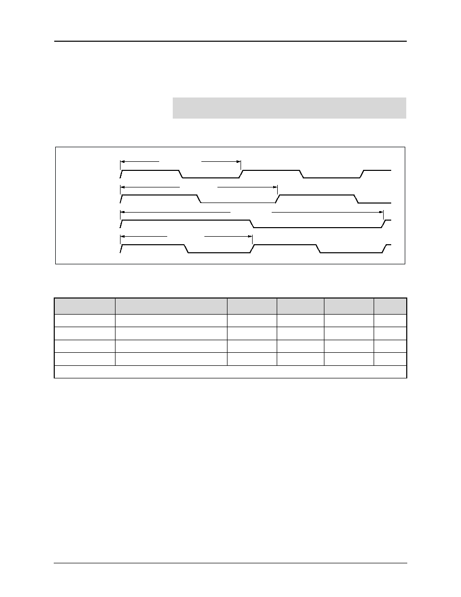
500238B
Mindspeed TechnologiesTM
9
-
3
Advance Information
CX29503 Data Sheet
Electrical and Mechanical Specifications
9.1.2
AC Characteristics
NOTE:
The
Figure 9-1
waveforms only specify edge relationships. They are not intended to
specify functional relationships between signals.
Figure 9-1. General Interface Timing Characteristics
T_clk_txe1
T_clk_txds1
T_clk_txe3
T_clk_txds3
I
CLK_TXDS3
I
CLK_TXE3
I
CLK_TXDS1
I
CLK_TXE1
100702 _047
Table 9-4. General Interface Timing Characteristics
Symbol
Parameter
Min
Typ
Max
Unit
T_clk_txds3
Clock period, CLK_TXDS3
≠20 ppm
22.3533
+20 ppm
ns
T_clk_txe3
Clock period, CLK_TXE3
≠20 ppm
29.0968
+20 ppm
ns
T_clk_txds1
Clock period, CLK_TXDS1
≠20 ppm
647.668
+20 ppm
ns
T_clk_txe1
Clock period, CLK_TXE1
≠20 ppm
488.281
+20 ppm
ns
GENERAL NOTE:
All clocks have a duty cycle requirement of 50%, ±5%.

9-4
Mindspeed TechnologiesTM
500238B
Advance Information
Electrical and Mechanical Specifications
CX29503 Data Sheet
Figure 9-2. SI-Bus Interface Timing Characteristics
100702_048
Tpd_sib_txprty
Tpd_sib_txdat
Thd_sib_rxprty
Tsu_sib_rxprty
Thd_sib_rxdat
Tsu_sib_rxdat
Thd_sib_rxstrt
Tsu_sib_rxstrt
T_sib_rxclk
T_sib_rxhsclk
Thd_sib_txstrt
Tsu_sib_txstrt
T_sib_txclk
T_sib_txhsclk
I SIB_TXHSCLK
I
SIB_TXCLK
I
SIB_TXSTRT
O
SIB_TXDAT
O
SIB_TXPRTY
I SIB_RXHSCLK
I
SIB_RXCLK
I
SIB_RXSTRT
I
SIB_RXDAT
I
SIB_RXPRTY
Table 9-5. SI-Bus Interface Timing Characteristics <tableContinuation>(1 of 2)
Symbol
Parameter
Min
Typ
Max
Unit
T_sib_txhsclk
Clock period, SIB_TXHSCLK
≠20 ppm
19.29
+20 ppm
ns
T_sib_txclk
Clock period, SIB_TXCLK
≠20 ppm
52.44
+20 ppm
ns
Tpd_sib_txdat
Prop delay, SIB_TXCLK to SIB_TXDAT
3
--
14
ns
Tpd_sib_txprty
Prop delay, SIB_TXCLK to SIB_TXPRTY
3
--
14
ns
T_sib_rxhsclk
Clock period, SIB_RXHSCLK
≠20 ppm
19.29
+20 ppm
ns
T_sib_rxclk
Clock period, SIB_RXCLK
≠20 ppm
52.44
+20 ppm
ns
Tsu_sib_txstrt
Setup time, SIB_TXSTRT to SIB_TXCLK
0
--
--
ns
Thd_sib_txstrt
Hold time, SIB_TXSTRT to SIB_TXCLK
2
--
--
ns
Tsu_sib_rxstrt
Setup time, SIB_RXSTRT to SIB_RXCLK
1
--
--
ns

500238B
Mindspeed TechnologiesTM
9
-
5
Advance Information
CX29503 Data Sheet
Electrical and Mechanical Specifications
Thd_sib_rxstrt
Hold time, SIB_RXSTRT to SIB_RXCLK
3
--
--
ns
Tsu_sib_rxdat
Setup time, SIB_RXDAT to SIB_RXCLK
1
--
--
ns
Thd_sib_rxdat
Hold time, SIB_RXDAT to SIB_RXCLK
3
--
--
ns
Tsu_sib_rxprty
Setup time, SIB_RXPRTY to SIB_RXCLK
1
--
--
ns
Thd_sib_rxprty
Hold time, SIB_RXPRTY to SIB_RXCLK
3
--
--
ns
Note(s): All clocks have a duty cycle requirement of 50%,
±
5%.
Table 9-5. SI-Bus Interface Timing Characteristics <tableContinuation>(2 of 2)
Symbol
Parameter
Min
Typ
Max
Unit
Figure 9-3. TSB Interface Timing Characteristics
100702_049
Tpd_tsb_ordat
Tpd_tsb_ordat
Tpd_tsb_orstuff
Tpd_tsb_orstuff
Tpd_tsb_otstuff
Tpd_tsb_otstuff
Tpd_tsb_ostb
Tpd_tsb_ostb
Tpd_tsb_rdat
Tpd_tsb_rdat
Tpd_tsb_rsync
Tpd_tsb_rsync
Tpd_tsb_rstuff
Tpd_tsb_rstuff
Tpd_tsb_tsynco
Tpd_tsb_tsynco
Tpd_tsb_tstuff
Tpd_tsb_tstuff
Tpd_tsb_stb
Tpd_tsb_stb
Tpw_tsb_ordat
Tpw_tsb_orstuff
Thd_tsb_otdat
Tsu_tsb_otdat
Tpw_tsb_otstuff
Tpw_tsb_ostb
T_tsb_oclk
Tpw_tsb_rdat
Tpw_tsb_rsync
Tpw_tsb_rstuff
Thd_tsb_tsynci
Tsu_tsb_tsynci
Thd_tsb_tdat
Tsu_tsb_tdat
Tpw_tsb_tsynco
Tpw_tsb_tstuff
Tpw_tsb_stb
T_tsb_clk
O
TSB_CLK
O
TSB_STB
O
TSB_TSTUFF
O
TSB_TSYNCO
I
TSB_TDAT
I
TSB_TSYNCI
O
TSB_RSTUFF
O
TSB_RSYNC
O
TSB_RDAT
O
TSB_OCLK
O
TSB_OSTB
O
TSB_OTSTUFF
I
TSB_OTDAT
O
TSB_ORSTUFF
O
TSB_ORDAT

9-6
Mindspeed TechnologiesTM
500238B
Advance Information
Electrical and Mechanical Specifications
CX29503 Data Sheet
Table 9-6. TSB Interface Timing Characteristics
Symbol
Parameter
Min
Typ
Max
Unit
T_tsb_clk
Clock period, TSB_CLK, SONET mode
≠20 ppm
19.29
+20 ppm
ns
T_tsb_clk
Clock period, TSB_CLK, DS3 mode
≠20 ppm
22.3533
+20 ppm
ns
T_tsb_clk
Clock period, TSB_CLK, E3 mode
≠20 ppm
29.0968
+20 ppm
ns
Tpd_tsb_stb
Prop delay, TSB_CLK to TSB_STB
0.5
--
5.0
ns
Tpw_tsb_stb
Pulse width, TSB_STB
8
◊
T_tsb_clk
8
◊
T_tsb_clk
8
◊
T_tsb_clk
ns
Tpd_tsb_tstuff
Prop delay, TSB_CLK to TSB_TSTUFF
0.5
--
5.0
ns
Tpw_tsb_tstuff
Pulse width, TSB_TSTUFF
8
◊
T_tsb_clk
8
◊
T_tsb_clk
8
◊
T_tsb_clk
ns
Tpd_tsb_tsynco
Prop delay, TSB_CLK to TSB_TSYNCO
0.5
--
5.0
ns
Tpw_tsb_tsynco
Pulse width, TSB_TSYNCO
T_tsb_clk
T_tsb_clk
T_tsb_clk
ns
Tsu_tsb_tdat
Setup time, TSB_TDAT to TSB_CLK
9
--
--
ns
Thd_tsb_tdat
Hold time, TSB_TDAT to TSB_CLK
≠3
--
--
ns
Tsu_tsb_tsynci
Setup time, TSB_SYNCI to TSB_CLK
9
--
--
ns
Thd_tsb_tsynci
Hold time, TSB_SYNCI to TSB_CLK
≠3
--
--
ns
Tpd_tsb_rstuff
Prop delay, TSB_CLK to TSB_RSTUFF
0.5
--
5.0
ns
Tpw_tsb_rstuff
Pulse width, TSB_RSTUFF
8
◊
T_tsb_clk
8
◊
T_tsb_clk
8
◊
T_tsb_clk
ns
Tpd_tsb_rsync
Prop delay, TSB_CLK to TSB_RSYNC
0.5
--
5.0
ns
Tpw_tsb_rsync
Pulse width, TSB_RSYNC
T_tsb_clk
T_tsb_clk
T_tsb_clk
ns
Tpd_tsb_rdat
Prop delay, TSB_CLK to TSB_RDAT
0.5
--
5.0
ns
Tpw_tsb_rdat
Pulse width, TSB_RDAT
T_tsb_clk
T_tsb_clk
T_tsb_clk
ns
T_tsb_oclk
Clock period, TSB_OCLK
4
◊
T_tsb_clk
4
◊
T_tsb_clk
4
◊
T_tsb_clk
ns
Tpd_tsb_ostb
Prop delay, TSB_OCLK to TSB_OSTB
-1
--
2
ns
Tpw_tsb_ostb
Pulse width, TSB_OSTB
8
◊
T_tsb_oclk
8
◊
T_tsb_oclk
8
◊
T_tsb_oclk
ns
Tpd_tsb_otstuff
Prop delay, TSB_OCLK to TSB_OTSTUFF
-1
--
2
ns
Tpw_tsb_otstuff
Pulse width, TSB_OTSTUFF
8
◊
T_tsb_oclk
8
◊
T_tsb_oclk
8
◊
T_tsb_oclk
ns
Tsu_tsb_otdat
Setup time, TSB_OTDAT to TSB_OCLK
10.8
--
--
ns
Thd_tsb_otdat
Hold time, TSB_OTDAT to TSB_OCLK
≠4.6
--
--
ns
Tpd_tsb_orstuff
Prop delay, TSB_OCLK to TSB_ORSTUFF
-1
--
2
ns
Tpw_tsb_orstuff
Pulse width, TSB_ORSTUFF
8
◊
T_tsb_oclk
8
◊
T_tsb_oclk
8
◊
T_tsb_oclk
ns
Tpd_tsb_ordat
Prop delay, TSB_CLK to TSB_ORDAT
-1
--
2
ns
Tpw_tsb_ordat
Pulse width, TSB_ORDAT
T_tsb_oclk
T_tsb_oclk
T_tsb_oclk
ns
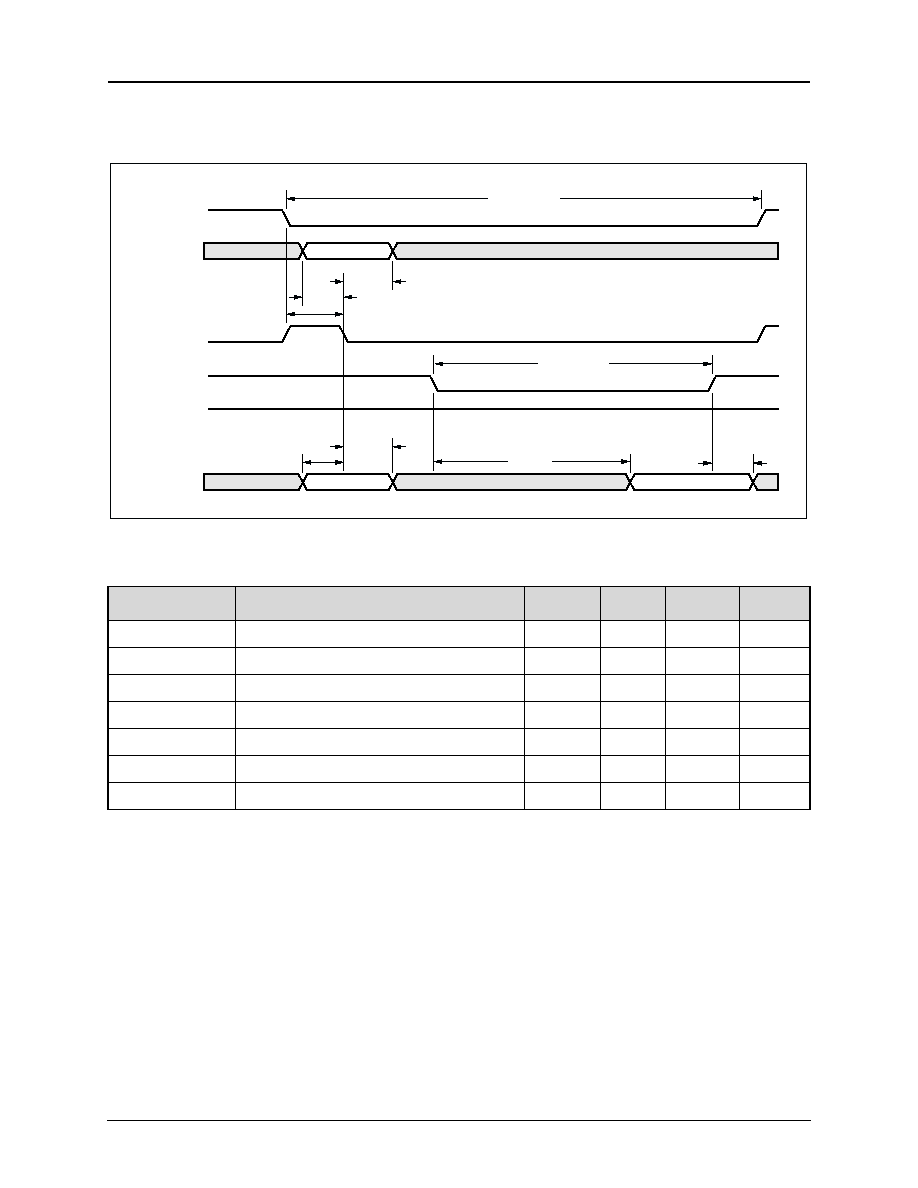
500238B
Mindspeed TechnologiesTM
9
-
7
Advance Information
CX29503 Data Sheet
Electrical and Mechanical Specifications
Figure 9-4. E-Bus Read Timing
Tpw_cs_n
Tpw_ds_n
Address[17:8]
Address[7:0]
Data
Tdis_d
Tpd_d
Thd_a
Tsu_a
Tsu_cs_n
Thd_a
Tsu_a
I
CS_N
I
A[17:8]
I
AS_N
I
DS_N
I
RW_N
I
AD
100702_052
Table 9-7. E-Bus Interface Read Timing Characteristics
Symbol
Parameter
Min
Typ
Max
Unit
Tpw_cs_n
Pulse width, CS_N
11
◊
31
--
--
ns
Tsu_cs_n
Setup time, CS_N to AS_N
31
--
--
ns
Tsu_a
Setup time, A to AS_N
31
--
--
ns
Thd_a
Hold time, A to AS_N
31
--
--
ns
Tpw_ds_n
Pulse width, DS_N
8
◊
31
--
--
ns
Tpd_d
Prop delay, DS_N to AD
7
◊
31
--
--
ns
Tdis_d
Disable time, DS_N to AD
31
--
--
ns

9-8
Mindspeed TechnologiesTM
500238B
Advance Information
Electrical and Mechanical Specifications
CX29503 Data Sheet
Figure 9-5. E-Bus Write Timing
Address[17:8]
Address[7:0]
Data
Thd_d
Tsu_d
Thd_a
Tsu_a
Tpw_rw_n
Tsu_cs_n
Thd_a
Tsu_a
Tpw_cs_n
I
CS_N
I
A[17:8]
I
AS_N
I
DS_N
I
RW_N
I
AD
100702_053
Table 9-8. E-Bus Interface Write Timing Characteristics
Symbol
Parameter
Min
Typ
Max
Unit
Tpw_cs_n
Pulse width, CS_N
11
◊
31
--
--
ns
Tsu_cs_n
Setup time, CS_N to AS_N
31
--
--
ns
Tsu_a
Setup time, A to AS_N
31
--
--
ns
Thd_a
Hold time, A to AS_N
31
--
--
ns
Tpw_rw_n
Pulse width, RW_N
8
◊
31
--
--
ns
Tsu_d
Setup time, RW_N to AD
7
◊
31
--
--
ns
Thd_d
Hold time, RW_N to AD
31
--
--
ns

500238B
Mindspeed TechnologiesTM
9
-
9
Advance Information
CX29503 Data Sheet
Electrical and Mechanical Specifications
Figure 9-6. Serial DS3/E3 Interface Timing
Tpd_txneg
Tpd_txneg
Tpd_txpos
Tpd_txpos
Thd_rxneg
Tsu_rxneg
Thd_rxneg
Tsu_rxneg
Thd_rxpos
Tsu_rxpos
Thd_rxpos
Tsu_rxpos
T_rlineclk
T_rxcki
T_tlineclk
I
TLINECLK
I
TXPOS
O
TXNEG
I
RXCKI
I
RLINECLK
I
RXPOS
I
RXNEG
500238_058
Table 9-9. Serial DS3/E3 Interface Characteristics
Symbol
Parameter
Min
Typ
Max
Unit
T_tlineclki
Clock Period, DS3 Mode, TLINECKI
- 20 ppm
22.3533
+ 20 ppm
ns
T_tlineclki
Clock Period, E3 Mode, TLINECLKI
- 20 ppm
29.0968
+ 20 ppm
ns
T_rlineclki
Clock Period, DS3 Mode, RLINECKI
- 20 ppm
22.3533
+ 20 ppm
ns
T_rlineclki
Clock Period, E3 Mode, RLINECLKI
- 20 ppm
29.0968
+ 20 ppm
ns
T_rxcki
Clock Period, DS3 Mode, RXCKI
- 20 ppm
22.3533
+ 20 ppm
ns
T_rxcki
Clock Period, E3 Mode, RXCKI
- 20 ppm
29.0968
+ 20 ppm
ns
Tduty_tlineclkj
Duty Cycle, TLINECLK
45
50
55
%
Tduty_rlineclkj
Duty Cycle, RLINECLK
45
50
55
%
Tduty_rlineclkj
Duty Cycle, RXCKI
45
50
55
%
Tpd_txpos
Prop Delay, TLINECLK to TXPOS
--
--
6
ns
Tpd_txneg
Prop De,lay, TLINECLK to TXNEG
--
--
6
ns
Tsu_rxpos
Setup Time, RXPOS to RLINECLK
5
--
--
ns
Thd_rxpos
Hold Time, RXPOS to RLINECLK
5
--
--
ns
Tsu_rxneg
Setup Time, RXNEG to RLINECLK
5
--
--
ns
Thd_rxneg
Hold Time, RXNEG to RLINECLK
5
--
--
ns

9-10
Mindspeed TechnologiesTM
500238B
Advance Information
Electrical and Mechanical Specifications
CX29503 Data Sheet
9.2
Mechanical Specification
This section specifies the mechanical characteristics of the package. This package is a
31
◊
31 mm, TBGA package with a heat spreader.

500238B
Mindspeed TechnologiesTM
9
-
11
Advance Information
CX29503 Data Sheet
Electrical and Mechanical Specifications
Figure 9-7. CX29503 Tape Ball Grid Array (TBGA), 324-Pin, 31 x 31 mm, 1.0 mm Ball Pitch
100702_046
A
1
2
3
4
5
6
7
8
9
10
11
12
13
14
15
16
17
18
19
20
21
22
23
24
25
26
27
28
29
30
B
C
D
E
F
G
H
J
K
L
M
N
P
R
T
U
V
W
Y
AA
AB
AC
AD
AE
AF
AG
AH
AJ
AK
D
D1
e
P
c
bbb C
A1
A
A
A1
D
D1
E
E1
b
c
M
N
aaa
bbb
e
P
1.25
0.40
30.80
30.80
0.50
0.85
0.15
1.55
0.60
31.20
31.20
0.75
0.95
0.15
0.25
1.40
0.50
31.00
29.00 BSC
31.00
29.00 BSC
0.63
0.90
31
324
1.00 TYP.
b
E
E1
aaa C
D
I
M
MIN.
NOM.
MAX.
REF: 324-Pin TBGA (GP00-D592)
All Dimensions
in Millimeters

9-12
Mindspeed TechnologiesTM
500238B
Advance Information
Electrical and Mechanical Specifications
CX29503 Data Sheet

500238B
Mindspeed TechnologiesTM
A
-
1
Advance Information
Appendix A: References
Standard
Title
ANSI
T1.107-1995
Digital Hierarchy--Formats Specifications
T1.105 -1995
SONET--Basic Description Including Multiplex Structure, Rates, and Formats
T1.105.02-1995
SONET--Payload Mappings
T1.105.04-1995
SONET--Data Communication Channel Protocols and Applications
T1.404-1994
Network to Customer Installation--DS3 Metallic Interface
T1.404a-1996
Supplement to ANSI T1.404-1994
Telcordia
GR-253-CORE
SONET Transport Systems: Common Generic Criteria
IETF
RFC-2495
Definition of Managed Objects for the DS1, E1, DS2, and E2 Interface Types
RFC-2496
Definition of Managed Objects for the DS3/E3 Interface Types
RFC-2558
Definition of Managed Objects for the SONET/SDH Interface Types
ITU-T
Recommendation G.732
Digital Multiplex Equipments Operating at the Third Order Bit Rate of 34,368 kbps and the
Fourth Order Bit Rate of 139,264 kbps and Using Positive Justification
Recommendation G.707
Network Node Interface for the Synchronous Digital Hierarchy (SDH)

A-2
Mindspeed TechnologiesTM
500238B
Advance Information
References
CX29503 Data Sheet

500238B
Mindspeed TechnologiesTM
B
-
1
Advance Information
Appendix B: Acronyms and
Abbreviations
ADC
Analog-to-Digital Converter
AFPS
Automatic Facility Protection Switching
AGC
Automatic Gain Control
AIB
Alarm Indication Bit
AIC
Application Identification Channel
AIS
Alarm Indication Signal
ALBO
Automatic Line Build Out
ALOS
Analog Loss of Signal
AMI
Alternate Mark Inversion
ANSI
American National Standards Institute
B8ZS
Binary with 8 Zero Substitution
BAM
Broadband Access Multiplexer
BER
Bit Error Rate
BERR
Bit Error Counter
BFA
Basic Frame Alignment
BIP-2
Bit Interleaved parity--2 bits
BOP
Bit-Oriented Protocol
BPV
Bipolar Violation
BSDL
Boundary Scan Description Language
CAS
Channel Associated Signaling
CCS
Common Channel Signaling
CERR
CRC Errors
CGA
Carrier Group Alarm
CI
Customer Installation
CLAD
Clock Rate Adapter
CLT
Clock and Test
CMOS
Complementary Metal Oxide Semiconductor
COFA
Change Of Frame Alignment
CP
C-bit Parity
CRC
Cyclic Redundancy Check
CSP
Command Status Processor
CSU
Channel Service Unit
DAC
Digital to Analog Converter
DCS
Digital Cross-Connect System

B-2
Mindspeed TechnologiesTM
500238B
Advance Information
Acronyms and Abbreviations
CX29503 Data Sheet
DDS
Digital Data System
DL
Data Link
DMI
Digital Multiplexed Interface
DPLL
Digital Phase Locked Loop
DPM
Driver Performance Monitor
DS1
Digital Signal Level 1
DSU
Data Service Unit
EOM
End-Of-Message
ESF
Extended Superframe
EXZ
Excessive Zeros
FAS
Frame Alignment Sequence (E1 Format)
FCC
Federal Communications Committee
FCS
Frame Check Sequence
FDL
Facility Data Link
FEAC
Far-End Alarm Control
FEBE
Far-End Block Error
FERR
Framing Bit Error
FIFO
First In, First Out
FPS
Frame Pattern Sequence
FRED
Loss of Frame-Obsolete Acronym
Fs
Framing, signaling
FS
Frame Set
Ft
Framing, terminal
HCDS
High-Capacity Digital Service
HDB3
High-Density Bipolar, 3
rd
HDLC
High-Level Data Link Controller
ICOT
Intercity and Outstate Trunk
IDLC
Integrated Digital Loop Carrier
IEC
Incoming Error Count
IER
Interrupt Enable Register
IRR
Interrupt Request Register
ISDN
Integrated Service Digital Network
ISR
Interrupt Status Register
ITU≠T
International Telegraph and Telephone Consultative
Committee
JAT
Jitter Attenuator
JCLK
Jitter Attenuated Clock
JTAG
Joint Test Action Group
LBO
Line Build Out
LC
Logical Channel
LCV
Line Code Violation

500238B
Mindspeed TechnologiesTM
B
-
3
Advance Information
CX29503 Data Sheet
Acronyms and Abbreviations
LEC
Local Exchange Carrier
LIU
Line Interface Unit
LOAS
Loss of Analog Signal
LOF
Loss Of Frame
LOS
Loss Of Signal
LSB
Least Significant Bit
MAIS
Multiframe AIS
MART
Maximum Average Reframe Time
MAS
Multiframe Alignment Sequence (CAS Format)
MAT
Metropolitan Area Trunk
MCSM
Micro-Coded State Machine
MERR
MFAS Error
MFAS
Multiframe Alignment Sequence (CRC4 format)
MOP
Message Oriented Protocol
MOS
Message Oriented Signaling
MPU
Microprocessor Interface
MQFP
Metric Quad Flat Pack
MSB
Most Significant Bit
muldem
Contraction for multiplexer/demultiplexer
MUX
Multiplexer
MVIP
Multi-Vendor Integration Protocol
MYEL
Multiframe Yellow Alarm
NCO
Numerical Controlled Oscillator
NDF
New Data Flags
NI
Network Interface
NRZ
Non-Return to Zero
OOF
Out-Of-Frame
PCM
Pulse Code Modulation
PDH
Plesiochronous Digital Hierarchy
PDV
Pulse Density Violation
PIC
Polyethylene-Insulated Cable
PLCC
Plastic Leaded Chip Carrier
PLL
Phase Locked Loop
PM
Performance Monitoring
PQFP
Plastic Quad Flat Pack
PRBS
Pseudo-Random Bit Sequence
PRI
Primary Rate Interface
PRM
Performance Report Message
PTT
Postal Telephone and Telegraph
QRSS
Quasi-Random Signal Source
RAI
Remote Alarm Indication

B-4
Mindspeed TechnologiesTM
500238B
Advance Information
Acronyms and Abbreviations
CX29503 Data Sheet
RAIS
Receive Alarm Indication Signal
RBOP
Bit-Oriented Protocol Detector
RBS
Robbed Bit Signaling
RCVR
Receiver
RDI
Remote Defect Indication
RDL1
Receive Data Link 1
RDL2
Receive Data Link 2
RDL3
External Receive Data Link
REI
Remote Error Indications
RFRAME
Receive Framer
RJAT
Receive Jitter Attenuator
RLIU
Receive Line Interface Unit
RLOF
Receive Loss Of Frame
RMAIS
Receive Multiframe AIS
RMF
Receive Multiframe
RPDV
Receive Pulse Density Violation
RPLL
Receive Phase Locked Loop
RSB
Receive System Bus
RSBI
Receive System Bus Interface
RSIG
Receive Signaling Buffer
RSLIP
Receive Slip Buffer
RXCLK
Receive Clock
RZCS
AMI/HDB3/B8ZS Line Decoder
SDH
Synchronous Digital Hierarchy
SEF
Severely Errored Frame
SERR
CAS Error
SF
Super Frame
SI-Bus
SONET Interleave Bus
SLC
Subscriber Loop Carrier
SONET
Synchronous Optical Network
SP
Superframe
SPE
Synchronous Payload Envelope
SS
Signal Source
TAP
Test Access Port
TBGA
Tape Ball Grid Array
TBOP
Bit Oriented Protocol Formatter
TDL
Terminal Data Link
TDL1
Transmit Data Link 1
TDL2
Transmit Data Link 2
TDL3
External Transmit Data Link
TDM
Time Division Multiplexed
TJAT
Transmit Jitter Attenuator
TLIU
Transmit Line Interface Unit
TLOS
Transmit Loss of Signal
TMF
Transmit Multiframe

500238B
Mindspeed TechnologiesTM
B
-
5
Advance Information
CX29503 Data Sheet
Acronyms and Abbreviations
TSB
Time Slot Bus
TSBI
Transmit System Bus Interface
TSIC
Time Slot Interchange
TSIG
Transmit Signaling Buffer
TSLIP
Transmit Slip Buffer
TZCS
AMI/HDB3/B8ZS Line Encoder
UI
Unit Interval
UIP
User Interface Program
UMC
Unassigned Mux Code
UNICODE
Universal Trunk Out of Service Code
UPI
Microprocessor Interface
UTP
Unshielded Twisted Pair
VC
Virtual Container
VCO
Voltage Controlled Oscillator
VCXO
Voltage Controlled Crystal Oscillator
VGA
Variable Gain Amplifier
VSP
Virtual Serial Port
VT
Virtual Tributary
XMTR
Digital Transmitter
YEL
Yellow Alarm
ZCS
Zero Code Suppression

B-6
Mindspeed TechnologiesTM
500238B
Advance Information
Acronyms and Abbreviations
CX29503 Data Sheet

500238B
Mindspeed TechnologiesTM
C
-
1
Advance Information
Appendix C: Revision History
Revision History
Revision
Level
Date
Description
A
Advance
January 2001
Initial Release. Document No.100702A
A
Advance
August 2002
Document No. 500238A
∑
Removed support for Motorola 68K microprocessor.
∑
Added register 0x0A to DS1/E1 framer block.
∑
Changed timing on TSB_TDAT (
Figure 2-19
).
∑
Moved location of InsAIS-P in Transmit Path
Overhead Control register (0x6200).
∑
Added M13/E13 channel numbers and cross-
references to DS1/E1 framer numbers.
∑
Updated Idd and Iddio consumption estimates.
∑
Updated timing information for:
1. MPC860
2. E-Bus
3. Serial DS3/E3
∑
Removed B3SZ/HDB3 encode/decode block. B3SZ/
HDB3 encoding/decoding is performed by DS3/E3
framer block.
∑
Deleted material related to TSB bypass.
∑
Added section about Unframed DS1/E1 Mode
∑
Added TSBUS TSB_TSYNCI interface timing
diagram
∑
Added TSBUS TSB_RSYNCI interface timing
diagram
∑
Added unframed link control registers
∑
Deleted material related to BSLIP.
∑
Deleted Error Inertion 1 and 2 control registers
∑
Updated absolute maximum ratings over operating
free-air temperature ratings table
∑
Other minor revisions
B
Advance
November 2002
Restored INS_YEL bit (bit #4) to register 0x72--Trans-
mit Frame Format (TFRM). Removed references to
PSLIP buffers.Removed support for MPC860 micropro-
cessor interface.

C-2
Mindspeed TechnologiesTM
500238B
Advance Information
Revision History
CX29503 Data Sheet

www.mindspeed.com
General Information:
U.S. and Canada: (800) 854-8099
International: (949) 483-6996
Headquarters - Newport Beach
4000 MacArthur Blvd. East Tower
Newport Beach, CA. 92660
