Data Sheet
28234-DSH-001-B
May 2003
RS8234
ATM ServiceSAR Plus with xBR Traffic Management
The RS8234 Service Segmentation and Reassembly Controller integrates ATM terminal
functions, PCI Bus Master and Slave controllers, and a UTOPIA interface with service
specific functions in a single package. The ServiceSAR Controller generates and
terminates ATM traffic as well as automatically scheduling cells for transmission. The
RS8234 is targeted at 155 Mbps throughput systems where the number of VCCs is
relatively large, or the performance of the overall system is critical. Examples of such
networking equipment include Routers, Ethernet switches, ATM Edge switches, or
Frame Relay switches.
Service-Specific Performance Accelerators
The RS8234 incorporates numerous service-specific features designed to accelerate
and enhance system performance. As examples, the RS8234 implements Echo
Suppression of LAN traffic via LECID filtering, and supports Frame Relay DE to CLP
interworking.
Advanced xBR Traffic Management
The xBR Traffic Manager in the RS8234 supports multiple ATM service categories.
This includes CBR, VBR (both single and dual leaky bucket), UBR, GFR (Guaranteed
Frame Rate) and ABR. The RS8234 manages each VCC independently. It dynamically
schedules segmentation traffic to comply with up to 16+CBR user-configured
scheduling priorities for the various traffic classes. Scheduling is controlled by a
Schedule Table configured by the user and based on a user-specified time reference.
ABR channels are managed in hardware according to user programmable ABR
templates. These templates tune the performance of the RS8234's ABR algorithms
to a specific system's or network's requirements
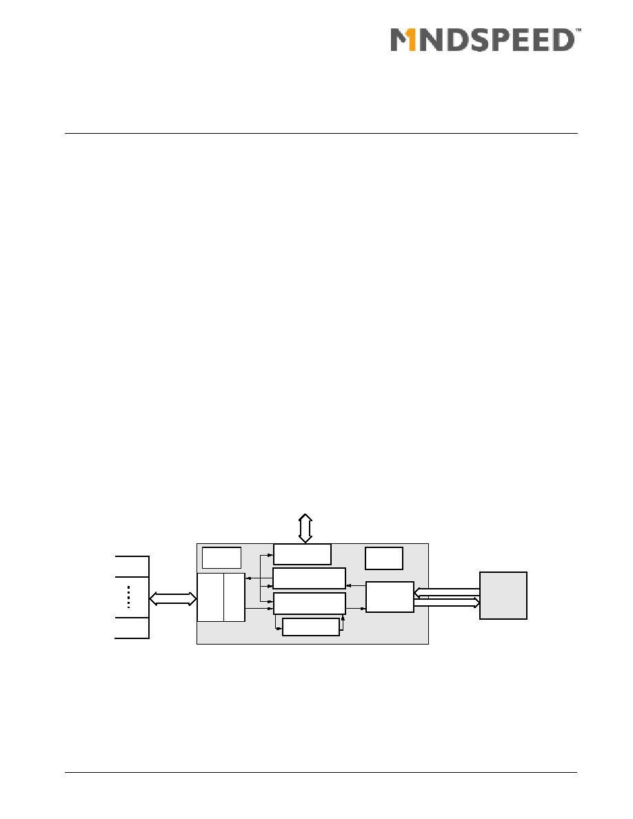
Functional Block Diagram
Multi-client
PCI Bus
Timer
Counters
Local Bus
PCI
Master/
Slave
DMA
Co-
Proc'r
Local Memory
Interface
Segmentation
Coprocessor
Reassembly
Coprocessor
CBR, VBR, ABR,
UBR, GFR
Traffic Manager
Patent Nos. 5,949,781
5,768,275
5,889,779
Rx/Tx
UTOPIA
Master/Slave
Control/
Status
RS8234
CN8250
PHY
Device
Cell
FIFO
Distinguishing Features
Service-Specific Performance
Accelerators
�
LECID filtering and echo suppression
�
Dual leaky bucket based on CLP
(frame relay)
�
Frame relay DE interworking
�
Internal SNMP MIB counters
�
IP over ATM; supports both CLP0+1
and ABR shaping
Flexible Architectures
�
Multi-peer host
�
Direct switch attachment via reverse
UTOPIA
�
ATM terminal
� Host control
� Local bus control
�
Optional local processor

28234-DSH-001-B
Mindspeed Technologies
TM
� 1998-2003,
Mindspeed TechnologiesTM, a Conexant business
All Rights Reserved.
Information in this document is provided in connection with Mindspeed Technologies ("Mindspeed") products. These materials are
provided by Mindspeed as a service to its customers and may be used for informational purposes only. Mindspeed assumes no
responsibility for errors or omissions in these materials. Mindspeed may make changes to specifications and product descriptions at
any time, without notice. Mindspeed makes no commitment to update the information and shall have no responsibility whatsoever for
conflicts or incompatibilities arising from future changes to its specifications and product descriptions.
No license, express or implied, by estoppel or otherwise, to any intellectual property rights is granted by this document. Except as
provided in Mindspeed's Terms and Conditions of Sale for such products, Mindspeed assumes no liability whatsoever.
THESE MATERIALS ARE PROVIDED "AS IS" WITHOUT WARRANTY OF ANY KIND, EITHER EXPRESS OR IMPLIED, RELATING
TO SALE AND/OR USE OF MINDSPEED PRODUCTS INCLUDING LIABILITY OR WARRANTIES RELATING TO FITNESS FOR A
PARTICULAR PURPOSE, CONSEQUENTIAL OR INCIDENTAL DAMAGES, MERCHANTABILITY, OR INFRINGEMENT OF ANY
PATENT, COPYRIGHT OR OTHER INTELLECTUAL PROPERTY RIGHT. MINDSPEED FURTHER DOES NOT WARRANT THE
ACCURACY OR COMPLETENESS OF THE INFORMATION, TEXT, GRAPHICS OR OTHER ITEMS CONTAINED WITHIN THESE
MATERIALS. MINDSPEED SHALL NOT BE LIABLE FOR ANY SPECIAL, INDIRECT, INCIDENTAL, OR CONSEQUENTIAL
DAMAGES, INCLUDING WITHOUT LIMITATION, LOST REVENUES OR LOST PROFITS, WHICH MAY RESULT FROM THE USE
OF THESE MATERIALS.
Mindspeed products are not intended for use in medical, lifesaving or life sustaining applications. Mindspeed customers using or
selling Mindspeed products for use in such applications do so at their own risk and agree to fully indemnify Mindspeed for any
damages resulting from such improper use or sale.
The following are trademarks of Conexant Systems, Inc.: Mindspeed TechnologiesTM, the MindspeedTM logo, and "Build It First"TM.
Product names or services listed in this publication are for identification purposes only, and may be trademarks of third parties.
Third-party brands and names are the property of their respective owners.
For additional disclaimer information, please consult Mindspeed Technologies Legal Information posted at
www.mindspeed.com
which is incorporated by reference.
Ordering Information
Revision History
Model Number
Package
Operating Temperatures
RS8234
388-pin BGA
�40
�
C
to 85
�
C

28234-DSH-001-B
Mindspeed Technologies
TM
Revision
Level
Date
Description
A
Advance
July 1998
Created.
N8234DS1B
RS8234 Rev. C
All changes to the device up through Rev. C are included in
this document. Specifically; increase in number of
scheduling priorities, increased number of allowed
VBR/ABR priorities, added scheduler control register,
programmable block size for VCI Index tables, improved
VPI/VCI lookup, added byte swapping for control bits,
additional field enables for Serial EEPROM and PCI
configuration space, programmable size of PCI address
space, added optional status queue interrupt delay, and
PCR limiting on priority queues.
E
Revision
July 2000
Revised.
500413A
Revision
November 2002
Revisions made. Changed format from Conexant to
Mindspeed.
28234-DSH-001-A
Revision
January 2003
New part number, corrected SCH_CTRL register bits
31-27 field size=5 and added bits 25-15 which were
missing. Corrected Table 14-2 by replacing 0x7000 with
0x1C00 in Notes section for BASE_PNTR field.
28234-DSH-001-B
Revision
May 2003
All changes denoted with change bars.

28234-DSH-001-B
Mindspeed Technologies
TM
Multi-Queue Segmentation Processing
The RS8234's segmentation coprocessor generates ATM cells for up to 64 K VCCs at a line rate of up to 200 Mbps for
simplex connections. The segmentation coprocessor formats cells on each channel according to segmentation VCC
Tables, utilizing up to 32 independent transmit queues and reporting segmentation status on a parallel set of up to 32
segmentation status queues. The segmentation coprocessor fetches client data from the host, formats ATM cells while
generating and appending protocol overhead, and forwards these to the UTOPIA port. The segmentation coprocessor
operates as a slave to the xBR Traffic Manager which schedules VCCs for transmission.
Multi-Queue Reassembly Processing
The RS8234's reassembly coprocessor stores the payload data from the cell stream received by the UTOPIA port into
host data buffers. Using a dynamic lookup method which supports NNI or UNI addressing, the reassembly coprocessor
processes up to 64 K VCCs simultaneously. The host supplies free buffers on up to 32 independent free buffer queues,
and the reassembly coprocessor performs all CPCS protocol checks and reports the results of these checks as well as
other status data on one of 32 independent reassembly status queues.
High Performance Host Architecture with Buffer Isolation
The RS8234 host interface architecture maximizes performance and system flexibility. The device's control and status
queues enable host/SAR communication via write operations alone. This lowers latency and PCI bus occupancy.
Flexibility is achieved by supporting a scalable peer-to-peer architecture. Multiple host clients may be addressed by the
SAR as separate physical or logical PCI peers. Segmentation and reassembly data buffers on the host system are
identified by buffer descriptors in SAR shared (or host) memory which contain pointers to buffers. The use of buffer
descriptors in this way allows for isolation of data buffers from the mechanisms that handle buffer allocation and
linking. This provides a layer of indirection in buffer assignment and management that maximizes system architecture
flexibility.
Designer Toolkit
Mindspeed provides an evaluation environment for the RS8234 which provides a working reference design, an example
software driver, and facilities for generating and terminating all service categories of ATM traffic. This system
accelerates ATM system development by providing a rapid prototyping environment.

28234-DSH-001-B
Mindspeed Technologies
TM
New Features
�
3.3 V, 388 BGA lowers power and
eases PCB assembly
�
AAL3/4 CPCS generation and
checking
�
PCI 2.1, including support for serial
EEPROM
�
Enhancements to xBR Traffic
Manager
� fewer ABR templates
� improved CBR tunneling
�
Reduced memory size for VCC
lookup tables
�
Increased addressing flexibility
�
Additional byte lane swappers for
increased system flexibility
xBR Traffic Management
�
TM 4.1 Service Classes
� CBR
� VBR (single, dual and CLP-based
leaky buckets)
� Real time VBR
� ABR
� UBR
� GFC (controlled & uncontrolled
flows)
� Guaranteed Frame Rate (GFR)
(guaranteed MCR on UBR VCCs)
�
16 Levels of priorities (16 + CBR)
�
Dynamic per-VCC scheduling
�
Multiple programmable ABR
templates (supplied by Mindspeed or
user)
�
Scheduler driven by local system
clock for low jitter CBR
�
Internal RM OAM cell feedback path
�
Virtual FIFO rate matching (Source
Rate Matching)
�
Per-VCC MCR and ICR.
�
Tunneling
� VP tunnels (VCI interleaving on
PDU boundaries)
� CBR tunnels (cells interleaved as
UBR, VBR or ABR with an
aggregate CBR limit)
Multi-Queue Segmentation Processing
�
32 transmit queues with optional
priority levels
�
64 K VCCs maximum *
�
AAL5 & AAL3/4 CPCS generation
�
AAL0 Null CPCS (optional use of PTI
for PDU demarcation)
�
ATM cell header generation
�
Raw cell mode (52 octet)
�
200 Mbps half duplex
�
155 Mbps full duplex (w/ 2-cell
PDUs)
�
Variable length transmit FIFO - CDV -
host latency matching (1 to 9 cells)
�
Symmetric Tx and Rx architecture
� buffer descriptors
� queues
�
User defined field circulates back to
the host (32 bits)
�
Distributed host or SAR shared
memory segmentation
�
Simultaneous segmentation and
reassembly
�
Per-PDU control of CLP/PTI (UBR)
�
Per-PDU control of AAL5 UU field
�
Message & streaming status modes
�
Virtual Tx FIFO (PCI host)
Multi-Queue Reassembly Processing
�
32 reassembly queues
�
64 K VCCs maximum *
�
AAL5 & AAL3/4 CPCS checking
�
AAL0
� PTI termination
� Cell count termination
�
Early Packet Discard, based on:
� Receive buffer underflow
� Receive status overflow
� CLP with priority threshold
� AAL5 max PDU length
� Rx FIFO full
� Frame relay DE with priority
threshold
� LECID filtering and echo
suppression
� Per-VCC firewalls
�
Dynamic channel lookup (NNI or UNI
addressing)
� Supports full address space
� Deterministic
� Flexible VCI count per VPI
� Optimized for signalling address
assignment
�
Message and streaming status
modes
�
Raw cell mode (52 octet)
�
200 Mbps half duplex
�
155 Mbps full duplex (w/ 2-cell
PDUs)
�
Distributed host or SAR shared
memory reassembly
�
8 Programmable reassembly
hardware time-outs (per-VCC
assignable)
�
Global max PDU length for AAL5
�
Per-VCC buffer firewall (memory
usage limit)
�
Simultaneous reassembly and
segmentation
�
Idle cell filtering
�
32 K duplex VCCs
High Performance Host Architecture
with Buffer Isolation
�
Write-only control and status
�
Read multiple command for data
transfer
�
Up to 32 host clients control and
status queues
�
Physical or logical clients
� Enables peer-to-peer architecture
�
Descriptor-based buffer chaining
�
Scatter/gather DMA
�
Endian neutral (allows data word and
control word byte swapping, for both
big and little endian systems)
�
Non-word (byte) aligned host buffer
addresses
�
Automatically detects presence of Tx
data or Rx free buffers
�
Virtual FIFOs (PCI bursts treated as a
single address)
�
Hardware indication of BOM
�
Allows isolation of system resources
�
Status queue interrupt delay
Designer Toolkit
�
Evaluation hardware and software
�
Reference schematics
�
Hardware Programming Interface -
RS823xHPI reference Source code
(C)
Generous Implementation of OAM-PM
Protocols
�
Detection of all F4/F5 OAM flows
�
Internal PM monitoring and
generation for up to 128 VCCs
�
Optional global OAM Rx/Tx queues
�
In-Line OAM insertion & generation
Standards-Based I/O
�
33 MHz PCI 2.1
�
Serial EEPROM to store PCI
configuration information
�
PHY interfaces
� UTOPIA master (Level 1)
� UTOPIA slave (Level 1)
�
Flexible SAR shared memory
architecture
�
Optional local control interface
�
Boundary scan for board-level testing
�
Source loopback, for diagnostics
�
Glueless connection to Mindspeed's
ATM physical layer device, the
RS8250

28234-DSH-001-B
Mindspeed Technologies
TM
Standards Compliance
�
UNI/NNI 3.1
�
TM 4.1
�
Bellcore GR-1248
�
ATM Forum B-ICI V2.0
�
I.363
�
I.610 /GR-1248
�
AToM MIB (RFC1695)
�
ILMI MIB
�
ANSI T1.635
�
GFC per I.361
�
SNMP
�
PCI Revision 2.1
�
IEEE 1149.1-1990
�
IEEE 1149.1 Supplement B, 1994
Electrical/Mechanical
�
388 BGA package
�
3.3 V power supply
�
5 V tolerant I/O pads
�
5 V � 3.3 V PCI pads
�
Low power 1.5 W (typical) @ full rate
�
Industrial temperature range
�
TTL level inputs
�
CMOS level outputs
Statistics and Write-Only Counters
�
Global register counter of # of cells
transmitted
�
Global register counter of # of cells
rcvd on active channels
�
Global register counter of # of cells
rcvd on inactive channels
�
Global register counter of # of AAL5
CPCS-PDUs discarded due to
per-channel firewall, etc.
�
RSM per-VCC service discard
counters (frame relay & LANE)
�
One programmable Interval Timer
(32 bits w/ interrupt)
�
per-VCC AAL3/4 MIB counters:
� # cells w/ CRC10 errors
� # cells w/ MID errors
� # cells w/ LI errors
� # cells w/ SN errors
� # cells w/ BOM or SSM errors
� # cells w/ EOM errors

28234-DSH-001-B
Mindspeed Technologies
TM

28234-DSH-001-B
Mindspeed Technologies
TM

28234-DSH-001-B
Mindspeed Technologies
TM
1-1
1
1.0 RS8234 Product Overview
1.1 Introduction
The RS8234 Service Segmentation and Reassembly Controller (ServiceSAR)
delivers a wide range of advanced ATM, AAL, and service-specific features in a
highly integrated CMOS package.
Some of the RS8234 service-level features provide system designers with
capabilities of accelerating specific protocol interworking functions. These
features include, for example, Virtual FIFO segmentation of circuit-based
Constant Bit Rate (CBR) traffic, and Frame Relay Early Packet Discard (EPD)
based on the Discard Eligibility (DE) field.
Other service-level functions enable network level functionality or topologies.
Two examples of these features include Generic Flow Control (GFC), and echo
suppression of multicast data frames on Emulated LAN (ELAN) channels.
In addition to meeting the requirements contained in UNI 3.1, the RS8234
complies with ATM Forum Traffic Management specification TM 4.1. The
RS8234 provides traffic shaping for all service categories:
�
CBR, Variable Bit Rate (VBR) -- both single and dual leaky bucket
�
Unspecified Bit Rate (UBR)
�
Available Bit Rate (ABR)
�
GFC -- both controlled and uncontrolled flows
�
Guaranteed Frame Rate (GFR), i.e., guaranteed Minimum Cell Rate
(MCR) on UBR Virtual Channel Connections (VCCs)
The internal xBR Traffic Manager automatically schedules each VCC according
to user assigned parameters.
The RS8234's architecture is designed to minimize and control host traffic
congestion. The host manages the RS8234 terminal using an efficient architecture
employing write-only control and status queues. For example, the host submits
data for transmit by writing buffer descriptor pointers to one of 32 Transmit
Queues. These entries can be thought of as task lists for the ServiceSAR to
perform. The RS8234 reports segmentation and reassembly status to the host by
writing entries to segmentation and reassembly status queues, which the host then
further processes. This architecture lessens the control burden on the host system
and minimizes Peripheral Component Interconnect (PCI) bus utilization by
eliminating reads across the PCI bus from host control activities.

1.0 RS8234 Product Overview
RS8234
1.1 Introduction
ATM ServiceSAR Plus with xBR Traffic Management
1-2
Mindspeed Technologies
TM
28234-DSH-001-B
The RS8234 host interface provides for control of host congestion through the
following mechanisms. First, each peer maintains separate control and status
queues. Then, each VCC in a peer group may be limited to a specific maximum
receive buffer utilization, further controlling congestion. EPD is supported for
VCCs that exceed their resource allotments. On transmit, peers are assigned fixed
or round robin priority to ensure predictable servicing. The host can implement a
congestion notification algorithm for ABR with a simple one-word write to an
SAR control register. The SAR will reduce the Explicit Rate (ER) field or set the
Congestion Indication (CI) bit in Turnaround (Resource Management (RM) cells,
based on user configuration.
The RS8234 consists of five separate coprocessors:
�
Incoming DMA,
�
Outgoing DMA,
�
Reassembly,
�
Segmentation, and
�
xBR Traffic Manager
Each coprocessor maintains state information in shared, off-chip memory.
This memory is controlled by the SAR through the local bus interface, which
arbitrates access to the bus between the various coprocessors. Although these
coprocessors run off the same system clock, they operate asynchronously from
each other. Communication between the coprocessors takes place through on-chip
FIFO buffers or through queues in SAR-shared memory (that is, memory local to
the SAR and accessible both to the SAR and the host).
The RS8234's on-chip coprocessor blocks are surrounded by high
performance PCI and UTOPIA ports for glueless interface to a variety of system
components with full line rate throughput and low bus occupancy.
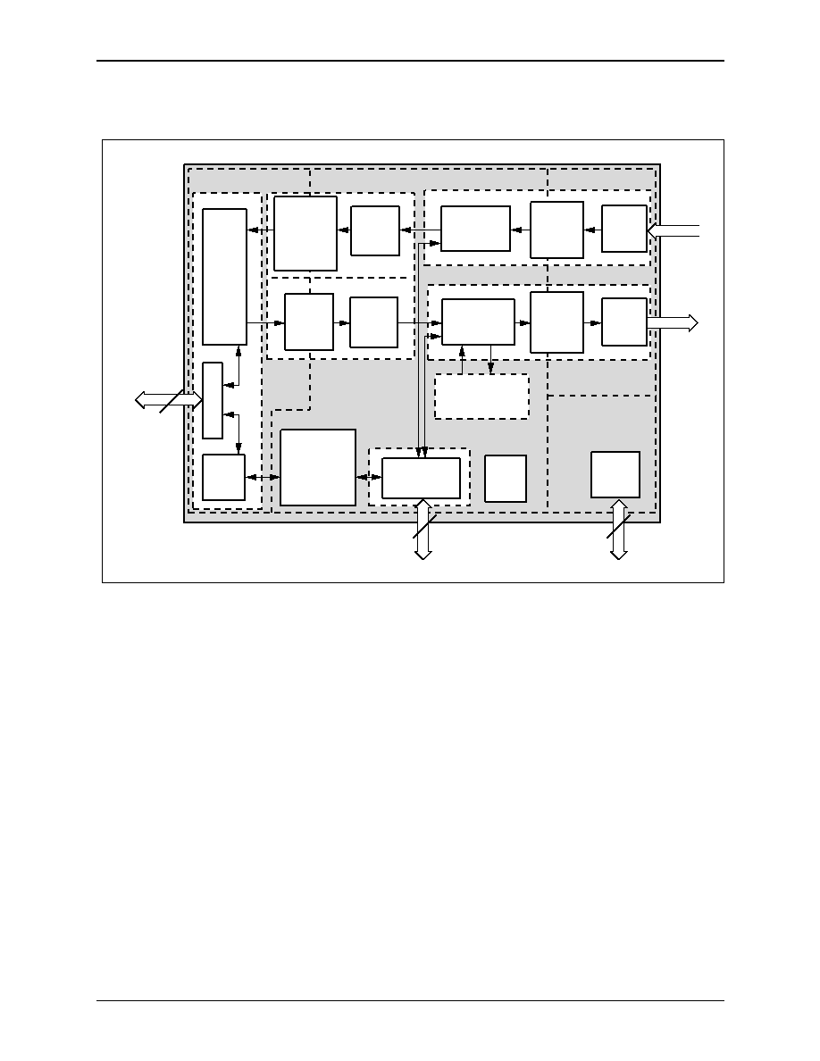
Figure 1-1
illustrates these functional blocks.
RS8234
1.0 RS8234 Product Overview
ATM ServiceSAR Plus with xBR Traffic Management
1.2 Service-Specific Performance Accelerators
28234-DSH-001-B
Mindspeed Technologies
TM
1-3
1.2 Service-Specific Performance Accelerators
The RS8234 incorporates several service-specific features, which accelerate
system performance. Some of these service level features provide the possibility
for designers to accelerate specific protocol interworking functions. Other service
level features enable network level functionality. These features are outlined in
Chapter 2.0
, and are fully described in succeeding chapters.
UNI or NNI Addressing
The RS8234 handles both User-Network Interface (UNI) addresses, which use an
8-bit Virtual Path Identifier (VPI) field, and Network-to-Network Interface (NNI)
addresses, which use a 12-bit VPI field.
Frame Relay Interworking
The VBR traffic category includes rate-shaping via the dual leaky bucket Generic
Cell Rate Algorithm (GCRA) based on the Cell Loss Priority (CLP) bit, for use in
Frame Relay. The RS8234 also implements the Frame Relay discard attribute by
Figure 1-1. RS8234 Functional Block Diagram
PCI Master/Slave
DMA Coprocessor
Reassembly Block
Segmentation Block
PCI
Clock
Domain
(System Clock
Domain)
Local Bus
Interface
xBR Traffic
Manager
(ATM PHY Interface
Clock Domain)
(Boundary Scan
Clock Domain)
PCI
Bus
Master
Logic
Dr
iv
ers
PCI
Slave
Logic
Control/Status
Registers,
Counters,
and
Internal SRAM
Memory
Arbiter
Clock/
Timer
(32 bit)
Boundary
Scan
Local Bus
60
Test Bus
5
PCI Bus
Interface
HOST
50
ATM
Physical
Receive
Interface
ATM
Physical
Transmit
Interface
12
12
Reassembly
Coprocessor
DMA
Outgoing
Channel
Burst
FIFO
(Depth =
64 bytes)
Segmentation
Coprocessor
Tx FIFO
(Depth =
512 bytes)
xBR Scheduler /
ABR Flow Control
Mgr.
Rx
FIFO
(Depth =
256 bytes)
Physical
Rx
Port
Physical
Tx
Port
DMA
Incoming
Channel
Burst FIFO
(Depth =
2048 bytes)
100074_001

1.0 RS8234 Product Overview
RS8234
1.2 Service-Specific Performance Accelerators
ATM ServiceSAR Plus with xBR Traffic Management
1-4
Mindspeed Technologies
TM
28234-DSH-001-B
performing early packet discard based on the frame's DE field and assigned
discard priority.
IP Interworking
The RS8234 facilitates ATM call control signalling procedures as defined in
ATM Forum's UNI Signalling 4.0 Specification (SIG 4.0), to support IP over
ATM environments. Some of the SIG 4.0 capabilities that are of interest to IP over
ATM and which the RS8234 allows for are as follows:
�
ABR signalling for point-to-point calls
�
Traffic parameter negotiation
�
Frame discard support
Guaranteed Frame Rate
The RS8234 can rate-shape ATM Adaptation Layer Type 5 (AAL5) Common Part
Convergence Sublayer Protocol Data Units (CPCS-PDUs, i.e., "frames") in the
UBR service category, by providing a guaranteed MCR for UBR VCCs.
Early Packet Discard
The EPD feature provides a mechanism to discard complete or partial
CPCS-PDUs based upon service discard attributes or error conditions. The
reassembly coprocessor performs EPD functions under the following conditions:
�
Frame Relay packet discard based on the DE field in the received frame
and the channel exceeding a user-defined priority threshold.
�
Packet discard based on the CLP bit.
�
LANE-LECID packet discard to implement echo suppression on multicast
data frames on ELAN channels.
�
Packet discard when a firewall condition occurs on a VCC or group.
�
Receive FIFO full condition/threshold.
�
Various AAL3/4 Management Information Base (MIB) errors.
CBR Traffic Handling
The segmentation coprocessor includes an internal rate-matching mechanism to
match the internal rate (the local reference rate) of CBR segmentation to an
external rate (the host rate).
The user can direct the RS8234 to segment traffic from a fixed PCI address
(i.e., a Virtual FIFO) for circuit-based CBR traffic.
The user can delineate up to sixteen CBR pipes (or tunnels) in which to
transmit multiple UBR, VBR, or ABR channels. In addition, the bandwidth of
any single tunnel can be shared by up to four different priorities of traffic, in
effect, establishing a multi-service tunnel. This allows proprietary management
schemes to operate under preallocated CBR bandwidths.
ABR Traffic Management
The ABR Flow Control Manager dynamically rate-shapes ABR traffic
independently per VCC, based upon network feedback. One or more ABR
templates are used to govern the behavior of traffic.
�
Both Relative Rate (RR) and ER algorithms are employed when
computing a rate adjustment on an ABR VCC.
�
Programmable ABR templates allow rate-shaping on groups of VCCs to

RS8234
1.0 RS8234 Product Overview
ATM ServiceSAR Plus with xBR Traffic Management
1.2 Service-Specific Performance Accelerators
28234-DSH-001-B
Mindspeed Technologies
TM
1-5
be tuned for different network policies.
�
New per-VCC MCR and ICR fields reduce the number of ABR templates
needed in local memory.
�
The RS8234 allows rate adjustments on Turnaround RM cells, based on
congestion in the host.
�
The RS8234 allows rate adjustments due to Use-It-Or-Lose-It behavior.
�
The RS8234 generates out-of-rate Forward RM cell(s) to restart
scheduling of a VCC whose rate has dropped below the Schedule Table
minimum rate.
�
The RS8234 optionally posts the current Allowed Cell Rate (ACR) on the
segmentation status queue for the host monitoring functions.
VBR Traffic Management
The RS8234 schedules each VBR VCC according to GCRA parameters stored in
the individual VCC control tables. The internal xBR Traffic Manager schedules
the transmitted data to maximize the permitted link utilization. The actual rate
sent is accurate to within 0.15% of the negotiated rates over a range from 10 cells
per second to full line rate of 155 Mbits/sec.
Three VBR modes are supported:
�
Sustained cell rate (one leaky bucket)
�
Peak and sustained cell rate (dual leaky bucket)
�
CLP 0+1 shaping (supports committed/best effort services)
(This is the mode recommended by the Internet Engineering Task Force
[IETF] as the most convenient model for IP over ATM interworking.)
Virtual Path Networking
The RS8234 can interleave segmentation of numerous VCCs (i.e., separate VC
channels) as members of one Virtual Path (VP). VP-based traffic shaping is
supported. The entire VP is scheduled according to parameters for one VCC.
AAL for Proprietary Traffic
The RS8234 incorporates an AAL0 traffic class for both segmentation and
reassembly, which acts as an AAL level for proprietary use. Several options for
packetization are implemented.
Optional Local Processing of ATM Management Traffic
The RS8234's Local Processor Interface allows for an optional local processor to
direct segmentation and reassembly of ATM management level traffic, such as
Operations and Maintenance (OAM) cells, Performance Monitoring (PM) cells,
signalling, and Interim Local Management Interface (ILMI) traffic. This
off-loads network control traffic from the host, thereby focusing host processing
power on the user application.
Internal SNMP MIB Counters
RS8234 has three internal counters that measure cells received, cells discarded,
and AAL5 PDUs discarded (to meet ILMI and RFC1695 requirements).

1.0 RS8234 Product Overview
RS8234
1.3 Designer Toolkit
ATM ServiceSAR Plus with xBR Traffic Management
1-6
Mindspeed Technologies
TM
28234-DSH-001-B
1.3 Designer Toolkit
The RS8234 ATM evaluation environment provides evaluation capability for the
RS8234 ServiceSAR. This environment serves as a hardware and software
reference design for development of customer-specific ATM applications. The
evaluation hardware and software was designed to provide a rapid prototyping
environment to assist and speed customer development of new ATM products,
thereby reducing product time to market.
This environment facilitates the following:
�
Assists and speeds customer product development
�
Provides hardware reference design
�
Provides software reference design (based on VxWorks)
�
Provides traffic generation and checking capability
Comprising part of this development environment is the RS8234/8250EVM, a
PCI card specifically designed to be a full-featured ATM controller implementing
the full functionality of the RS8234 ServiceSAR. The RS8234 resides at the heart
of this PCI card.
The PCI interface between the host processor and the local system is
controlled by Mindspeed's Hardware Programming Interface (RS823xHPI), a
software driver to the RS8234, on top of which a system designer can develop and
place proprietary driver software. This interface allows users to easily port their
applications to the RS8234. This software is written in C, and Source code is
available under license agreement.
The evaluation environment also includes a full set of design schematics, as
well as artwork for the RS8234EVM PCI card.

28234-DSH-001-B
Mindspeed Technologies
TM
7
Table of Contents
1.0
RS8234 Product Overview
. . . . . . . . . . . . . . . . . . . . . . . . . . . . . . . . . . . . . . . . . . . . . . . . . . . . . . . 1-1
1.1
Introduction
. . . . . . . . . . . . . . . . . . . . . . . . . . . . . . . . . . . . . . . . . . . . . . . . . . . . . . . . . . . . . . . 1-1
1.2
Service-Specific Performance Accelerators
. . . . . . . . . . . . . . . . . . . . . . . . . . . . . . . . . . . . . . . 1-3
1.3
Designer Toolkit
. . . . . . . . . . . . . . . . . . . . . . . . . . . . . . . . . . . . . . . . . . . . . . . . . . . . . . . . . . . . 1-6
Table of Contents
. . . . . . . . . . . . . . . . . . . . . . . . . . . . . . . . . . . . . . . . . . . . . . . . . . . . . . . . . . . . . . . 1-7
List of Figures
. . . . . . . . . . . . . . . . . . . . . . . . . . . . . . . . . . . . . . . . . . . . . . . . . . . . . . . . . . . . . . . . . 1-17
List of Tables
. . . . . . . . . . . . . . . . . . . . . . . . . . . . . . . . . . . . . . . . . . . . . . . . . . . . . . . . . . . . . . . . . . 1-21
2.0
Architecture Overview
. . . . . . . . . . . . . . . . . . . . . . . . . . . . . . . . . . . . . . . . . . . . . . . . . . . . . . . . . . 2-1
2.1
Introduction
. . . . . . . . . . . . . . . . . . . . . . . . . . . . . . . . . . . . . . . . . . . . . . . . . . . . . . . . . . . . . . . 2-1
2.2
High Performance Host Architecture with Buffer Isolation
. . . . . . . . . . . . . . . . . . . . . . . . . . . . . 2-2
2.2.1 Multiple ATM Clients
. . . . . . . . . . . . . . . . . . . . . . . . . . . . . . . . . . . . . . . . . . . . . . . . . . . . . 2-2
2.2.2 RS8234 Queue Structure
. . . . . . . . . . . . . . . . . . . . . . . . . . . . . . . . . . . . . . . . . . . . . . . . . . 2-3
2.2.3 Buffer Isolation Using Descriptor-Based Buffer Chaining
. . . . . . . . . . . . . . . . . . . . . . . . . . . 2-6
2.2.4 Status Queue Relation to Buffers and Descriptors
. . . . . . . . . . . . . . . . . . . . . . . . . . . . . . . . 2-8
2.2.5 Write-Only Control/Status
. . . . . . . . . . . . . . . . . . . . . . . . . . . . . . . . . . . . . . . . . . . . . . . . 2-10
2.2.6 Scatter/Gather DMA
. . . . . . . . . . . . . . . . . . . . . . . . . . . . . . . . . . . . . . . . . . . . . . . . . . . . . 2-10
2.2.7 Interrupts
. . . . . . . . . . . . . . . . . . . . . . . . . . . . . . . . . . . . . . . . . . . . . . . . . . . . . . . . . . . . 2-11
2.3
Automated Segmentation Engine
. . . . . . . . . . . . . . . . . . . . . . . . . . . . . . . . . . . . . . . . . . . . . . 2-12
2.4
Automated Reassembly Engine
. . . . . . . . . . . . . . . . . . . . . . . . . . . . . . . . . . . . . . . . . . . . . . . . 2-14
2.5
Advanced xBR Traffic Management
. . . . . . . . . . . . . . . . . . . . . . . . . . . . . . . . . . . . . . . . . . . . . 2-16
2.5.1 CBR Traffic
. . . . . . . . . . . . . . . . . . . . . . . . . . . . . . . . . . . . . . . . . . . . . . . . . . . . . . . . . . . 2-18
2.5.2 VBR Traffic
. . . . . . . . . . . . . . . . . . . . . . . . . . . . . . . . . . . . . . . . . . . . . . . . . . . . . . . . . . . 2-18
2.5.3 ABR Traffic
. . . . . . . . . . . . . . . . . . . . . . . . . . . . . . . . . . . . . . . . . . . . . . . . . . . . . . . . . . . 2-19
2.5.4 UBR Traffic
. . . . . . . . . . . . . . . . . . . . . . . . . . . . . . . . . . . . . . . . . . . . . . . . . . . . . . . . . . . 2-19
2.5.5 GFR Traffic
. . . . . . . . . . . . . . . . . . . . . . . . . . . . . . . . . . . . . . . . . . . . . . . . . . . . . . . . . . . 2-19
2.5.6 xBR Cell Scheduler
. . . . . . . . . . . . . . . . . . . . . . . . . . . . . . . . . . . . . . . . . . . . . . . . . . . . . 2-20
2.5.7 ABR Flow Control Manager
. . . . . . . . . . . . . . . . . . . . . . . . . . . . . . . . . . . . . . . . . . . . . . . 2-21
2.6
Burst FIFO Buffers
. . . . . . . . . . . . . . . . . . . . . . . . . . . . . . . . . . . . . . . . . . . . . . . . . . . . . . . . . . 2-22
2.7
Implementation of OAM-PM Protocols
. . . . . . . . . . . . . . . . . . . . . . . . . . . . . . . . . . . . . . . . . . 2-23

Table of Contents
RS8234
ATM ServiceSAR Plus with xBR Traffic Management
8
Mindspeed Technologies
TM
28234-DSH-001-B
2.8
Standards-Based I/O
. . . . . . . . . . . . . . . . . . . . . . . . . . . . . . . . . . . . . . . . . . . . . . . . . . . . . . . . 2-24
2.9
Electrical/Mechanical
. . . . . . . . . . . . . . . . . . . . . . . . . . . . . . . . . . . . . . . . . . . . . . . . . . . . . . . 2-25
2.10 Logic Diagram and Pin Descriptions
. . . . . . . . . . . . . . . . . . . . . . . . . . . . . . . . . . . . . . . . . . . . 2-25
3.0
Host Interface
. . . . . . . . . . . . . . . . . . . . . . . . . . . . . . . . . . . . . . . . . . . . . . . . . . . . . . . . . . . . . . . . . . 3-1
3.1
Overview
. . . . . . . . . . . . . . . . . . . . . . . . . . . . . . . . . . . . . . . . . . . . . . . . . . . . . . . . . . . . . . . . . . 3-1
3.2
Multiple Client Architecture
. . . . . . . . . . . . . . . . . . . . . . . . . . . . . . . . . . . . . . . . . . . . . . . . . . . 3-2
3.2.1 Logical Clients
. . . . . . . . . . . . . . . . . . . . . . . . . . . . . . . . . . . . . . . . . . . . . . . . . . . . . . . . . . 3-2
3.2.2 Resource Allocation
. . . . . . . . . . . . . . . . . . . . . . . . . . . . . . . . . . . . . . . . . . . . . . . . . . . . . . 3-3
3.2.3 Resource Isolation
. . . . . . . . . . . . . . . . . . . . . . . . . . . . . . . . . . . . . . . . . . . . . . . . . . . . . . . 3-3
3.2.4 Peer-to-Peer Transfers
. . . . . . . . . . . . . . . . . . . . . . . . . . . . . . . . . . . . . . . . . . . . . . . . . . . . 3-4
3.2.5 Local Processor Clients
. . . . . . . . . . . . . . . . . . . . . . . . . . . . . . . . . . . . . . . . . . . . . . . . . . . 3-5
3.3
Write-Only Control and Status
. . . . . . . . . . . . . . . . . . . . . . . . . . . . . . . . . . . . . . . . . . . . . . . . . . 3-6
3.3.1 Write-Only Control Queues
. . . . . . . . . . . . . . . . . . . . . . . . . . . . . . . . . . . . . . . . . . . . . . . . 3-6
3.3.1.1 Control Variables
. . . . . . . . . . . . . . . . . . . . . . . . . . . . . . . . . . . . . . . . . . . . . . . 3-7
3.3.1.2 Queue Management
. . . . . . . . . . . . . . . . . . . . . . . . . . . . . . . . . . . . . . . . . . . . . 3-7
3.3.1.3 Underflow Conditions
. . . . . . . . . . . . . . . . . . . . . . . . . . . . . . . . . . . . . . . . . . . . 3-8
3.3.2 Write-only Status Queues
. . . . . . . . . . . . . . . . . . . . . . . . . . . . . . . . . . . . . . . . . . . . . . . . . 3-9
3.3.2.1 Control Variables
. . . . . . . . . . . . . . . . . . . . . . . . . . . . . . . . . . . . . . . . . . . . . . . 3-9
3.3.2.2 Queue Management
. . . . . . . . . . . . . . . . . . . . . . . . . . . . . . . . . . . . . . . . . . . . 3-10
3.3.2.3 Overflow Conditions
. . . . . . . . . . . . . . . . . . . . . . . . . . . . . . . . . . . . . . . . . . . . 3-11
3.3.2.4 Status Queue Interrupt Delay
. . . . . . . . . . . . . . . . . . . . . . . . . . . . . . . . . . . . . 3-11
4.0
Segmentation Coprocessor
. . . . . . . . . . . . . . . . . . . . . . . . . . . . . . . . . . . . . . . . . . . . . . . . . . . . . . 4-1
4.1
Overview
. . . . . . . . . . . . . . . . . . . . . . . . . . . . . . . . . . . . . . . . . . . . . . . . . . . . . . . . . . . . . . . . . . 4-1
4.2
Segmentation Functional Description
. . . . . . . . . . . . . . . . . . . . . . . . . . . . . . . . . . . . . . . . . . . . 4-2
4.2.1 Segmentation VCCs
. . . . . . . . . . . . . . . . . . . . . . . . . . . . . . . . . . . . . . . . . . . . . . . . . . . . . . 4-2
4.2.1.1 Segmentation VCC Table
. . . . . . . . . . . . . . . . . . . . . . . . . . . . . . . . . . . . . . . . . . 4-2
4.2.1.2 VCC Identification
. . . . . . . . . . . . . . . . . . . . . . . . . . . . . . . . . . . . . . . . . . . . . . . 4-3
4.2.2 Submitting Segmentation Data
. . . . . . . . . . . . . . . . . . . . . . . . . . . . . . . . . . . . . . . . . . . . . . 4-4
4.2.2.1 User Data Format
. . . . . . . . . . . . . . . . . . . . . . . . . . . . . . . . . . . . . . . . . . . . . . . 4-4
4.2.2.2 Buffer Descriptors
. . . . . . . . . . . . . . . . . . . . . . . . . . . . . . . . . . . . . . . . . . . . . . 4-4
4.2.2.3 Host Linked Segmentation Buffer Descriptors
. . . . . . . . . . . . . . . . . . . . . . . . . . 4-5
4.2.2.4 Transmit Queues
. . . . . . . . . . . . . . . . . . . . . . . . . . . . . . . . . . . . . . . . . . . . . . . 4-5
4.2.2.5 Partial PDUs
. . . . . . . . . . . . . . . . . . . . . . . . . . . . . . . . . . . . . . . . . . . . . . . . . . . 4-7
4.2.2.6 Virtual Paths
. . . . . . . . . . . . . . . . . . . . . . . . . . . . . . . . . . . . . . . . . . . . . . . . . . 4-7
4.2.3 CPCS-PDU Processing
. . . . . . . . . . . . . . . . . . . . . . . . . . . . . . . . . . . . . . . . . . . . . . . . . . . . 4-8
4.2.3.1 AAL5
. . . . . . . . . . . . . . . . . . . . . . . . . . . . . . . . . . . . . . . . . . . . . . . . . . . . . . . . 4-8
4.2.3.2 AAL3/4
. . . . . . . . . . . . . . . . . . . . . . . . . . . . . . . . . . . . . . . . . . . . . . . . . . . . . . . 4-9

RS8234
Table of Contents
ATM ServiceSAR Plus with xBR Traffic Management
28234-DSH-001-B
Mindspeed Technologies
TM
9
4.2.3.3 AAL0
. . . . . . . . . . . . . . . . . . . . . . . . . . . . . . . . . . . . . . . . . . . . . . . . . . . . . . . 4-11
4.2.4 ATM Physical Layer Interface
. . . . . . . . . . . . . . . . . . . . . . . . . . . . . . . . . . . . . . . . . . . . . . 4-11
4.2.5 Status Reporting
. . . . . . . . . . . . . . . . . . . . . . . . . . . . . . . . . . . . . . . . . . . . . . . . . . . . . . . 4-12
4.2.6 Virtual FIFOs
. . . . . . . . . . . . . . . . . . . . . . . . . . . . . . . . . . . . . . . . . . . . . . . . . . . . . . . . . . 4-12
4.3
Segmentation Control and Data Structures
. . . . . . . . . . . . . . . . . . . . . . . . . . . . . . . . . . . . . . . 4-13
4.3.1 Segmentation VCC Table Entry
. . . . . . . . . . . . . . . . . . . . . . . . . . . . . . . . . . . . . . . . . . . . . 4-13
4.3.2 Data Buffers
. . . . . . . . . . . . . . . . . . . . . . . . . . . . . . . . . . . . . . . . . . . . . . . . . . . . . . . . . . 4-18
4.3.3 Segmentation Buffer Descriptors
. . . . . . . . . . . . . . . . . . . . . . . . . . . . . . . . . . . . . . . . . . . 4-18
4.3.4 Transmit Queues
. . . . . . . . . . . . . . . . . . . . . . . . . . . . . . . . . . . . . . . . . . . . . . . . . . . . . . . 4-21
4.3.4.1 Entry Format
. . . . . . . . . . . . . . . . . . . . . . . . . . . . . . . . . . . . . . . . . . . . . . . . . 4-21
4.3.4.2 Transmit Queue Management
. . . . . . . . . . . . . . . . . . . . . . . . . . . . . . . . . . . . . 4-22
4.3.5 Segmentation Status Queues
. . . . . . . . . . . . . . . . . . . . . . . . . . . . . . . . . . . . . . . . . . . . . . 4-23
4.3.5.1 Entry Format
. . . . . . . . . . . . . . . . . . . . . . . . . . . . . . . . . . . . . . . . . . . . . . . . . 4-23
4.3.5.2 Status Queue Management
. . . . . . . . . . . . . . . . . . . . . . . . . . . . . . . . . . . . . . . 4-23
4.3.5.3 Status Queue Overflow
. . . . . . . . . . . . . . . . . . . . . . . . . . . . . . . . . . . . . . . . . . 4-24
4.3.6 Segmentation Internal SRAM Memory Map
. . . . . . . . . . . . . . . . . . . . . . . . . . . . . . . . . . . 4-25
5.0
Reassembly Coprocessor
. . . . . . . . . . . . . . . . . . . . . . . . . . . . . . . . . . . . . . . . . . . . . . . . . . . . . . . 5-1
5.1
Overview
. . . . . . . . . . . . . . . . . . . . . . . . . . . . . . . . . . . . . . . . . . . . . . . . . . . . . . . . . . . . . . . . . . 5-1
5.2
Reassembly Functional Description
. . . . . . . . . . . . . . . . . . . . . . . . . . . . . . . . . . . . . . . . . . . . . 5-2
5.2.1 Reassembly VCCs
. . . . . . . . . . . . . . . . . . . . . . . . . . . . . . . . . . . . . . . . . . . . . . . . . . . . . . . 5-3
5.2.1.1 Relation to Segmentation VCCs
. . . . . . . . . . . . . . . . . . . . . . . . . . . . . . . . . . . . . 5-3
5.2.2 Channel Lookup
. . . . . . . . . . . . . . . . . . . . . . . . . . . . . . . . . . . . . . . . . . . . . . . . . . . . . . . . 5-4
5.2.2.1 Programmable Block Size for VCC Table/ VCI Index Table
. . . . . . . . . . . . . . . . . . 5-5
5.2.2.2 Setup
. . . . . . . . . . . . . . . . . . . . . . . . . . . . . . . . . . . . . . . . . . . . . . . . . . . . . . . . 5-6
5.2.2.3 Operation
. . . . . . . . . . . . . . . . . . . . . . . . . . . . . . . . . . . . . . . . . . . . . . . . . . . . . 5-6
5.2.2.4 AAL3/4 Lookup
. . . . . . . . . . . . . . . . . . . . . . . . . . . . . . . . . . . . . . . . . . . . . . . . 5-7
5.3
CPCS-PDU Processing
. . . . . . . . . . . . . . . . . . . . . . . . . . . . . . . . . . . . . . . . . . . . . . . . . . . . . . . 5-8
5.3.1 AAL5 Processing
. . . . . . . . . . . . . . . . . . . . . . . . . . . . . . . . . . . . . . . . . . . . . . . . . . . . . . . . 5-9
5.3.1.1 AAL5 COM Processing
. . . . . . . . . . . . . . . . . . . . . . . . . . . . . . . . . . . . . . . . . . . 5-9
5.3.1.2 AAL5 EOM Processing
. . . . . . . . . . . . . . . . . . . . . . . . . . . . . . . . . . . . . . . . . . . 5-9
5.3.1.3 AAL5 Error Conditions
. . . . . . . . . . . . . . . . . . . . . . . . . . . . . . . . . . . . . . . . . . 5-11
5.3.2 AAL3/4 Processing
. . . . . . . . . . . . . . . . . . . . . . . . . . . . . . . . . . . . . . . . . . . . . . . . . . . . . 5-12
5.3.2.1 AAL3/4 Per-Cell Processing
. . . . . . . . . . . . . . . . . . . . . . . . . . . . . . . . . . . . . . 5-13
5.3.2.2 AAL3/4 Additional BOM/SSM Processing
. . . . . . . . . . . . . . . . . . . . . . . . . . . . 5-14
5.3.2.3 AAL3/4 Additional COM Processing
. . . . . . . . . . . . . . . . . . . . . . . . . . . . . . . . . 5-14
5.3.2.4 AAL3/4 Additional EOM/SSM Processing
. . . . . . . . . . . . . . . . . . . . . . . . . . . . . 5-15
5.3.2.5 AAL3/4 MIB Counters
. . . . . . . . . . . . . . . . . . . . . . . . . . . . . . . . . . . . . . . . . . . 5-15
5.3.3 AAL0 Processing
. . . . . . . . . . . . . . . . . . . . . . . . . . . . . . . . . . . . . . . . . . . . . . . . . . . . . . . 5-15
5.3.3.1 Termination Methods
. . . . . . . . . . . . . . . . . . . . . . . . . . . . . . . . . . . . . . . . . . . 5-15
5.3.3.2 AAL0 Error Conditions
. . . . . . . . . . . . . . . . . . . . . . . . . . . . . . . . . . . . . . . . . . 5-16
5.3.4 ATM Header Processing
. . . . . . . . . . . . . . . . . . . . . . . . . . . . . . . . . . . . . . . . . . . . . . . . . . 5-16
5.3.5 BOM Synchronization Signal
. . . . . . . . . . . . . . . . . . . . . . . . . . . . . . . . . . . . . . . . . . . . . . 5-17
5.4
Buffer Management
. . . . . . . . . . . . . . . . . . . . . . . . . . . . . . . . . . . . . . . . . . . . . . . . . . . . . . . . 5-18
5.4.1 Host vs. Local Reassembly
. . . . . . . . . . . . . . . . . . . . . . . . . . . . . . . . . . . . . . . . . . . . . . . 5-18

Table of Contents
RS8234
ATM ServiceSAR Plus with xBR Traffic Management
10
Mindspeed Technologies
TM
28234-DSH-001-B
5.4.2 Scatter Method
. . . . . . . . . . . . . . . . . . . . . . . . . . . . . . . . . . . . . . . . . . . . . . . . . . . . . . . . 5-19
5.4.3 Free Buffer Queues
. . . . . . . . . . . . . . . . . . . . . . . . . . . . . . . . . . . . . . . . . . . . . . . . . . . . . 5-20
5.4.4 Linked Data Buffers
. . . . . . . . . . . . . . . . . . . . . . . . . . . . . . . . . . . . . . . . . . . . . . . . . . . . . 5-22
5.4.5 Initialization of Buffer Structures
. . . . . . . . . . . . . . . . . . . . . . . . . . . . . . . . . . . . . . . . . . . 5-23
5.4.5.1 Buffer Descriptors
. . . . . . . . . . . . . . . . . . . . . . . . . . . . . . . . . . . . . . . . . . . . . 5-23
5.4.5.2 Free Buffer Queue Base Table
. . . . . . . . . . . . . . . . . . . . . . . . . . . . . . . . . . . . . 5-23
5.4.5.3 Free Buffer Queue Entries
. . . . . . . . . . . . . . . . . . . . . . . . . . . . . . . . . . . . . . . . 5-23
5.4.5.4 Other Initialization
. . . . . . . . . . . . . . . . . . . . . . . . . . . . . . . . . . . . . . . . . . . . . 5-23
5.4.6 Buffer Allocation
. . . . . . . . . . . . . . . . . . . . . . . . . . . . . . . . . . . . . . . . . . . . . . . . . . . . . . . 5-24
5.4.7 Error Conditions
. . . . . . . . . . . . . . . . . . . . . . . . . . . . . . . . . . . . . . . . . . . . . . . . . . . . . . . 5-24
5.4.8 Early Packet Discard
. . . . . . . . . . . . . . . . . . . . . . . . . . . . . . . . . . . . . . . . . . . . . . . . . . . . 5-25
5.4.8.1 General Description
. . . . . . . . . . . . . . . . . . . . . . . . . . . . . . . . . . . . . . . . . . . . 5-25
5.4.8.2 Frame Relay Packet Discard
. . . . . . . . . . . . . . . . . . . . . . . . . . . . . . . . . . . . . . 5-25
5.4.8.3 CLP Packet Discard
. . . . . . . . . . . . . . . . . . . . . . . . . . . . . . . . . . . . . . . . . . . . 5-25
5.4.8.4 LANE-LECID Packet Discard--Echo Suppression on Multicast Data Frames
. . . 5-25
5.4.8.5 DMA FIFO Full
. . . . . . . . . . . . . . . . . . . . . . . . . . . . . . . . . . . . . . . . . . . . . . . . 5-26
5.4.8.6 AAL3/4 Early Packet Discard Processing
. . . . . . . . . . . . . . . . . . . . . . . . . . . . . 5-27
5.4.8.7 Error Conditions
. . . . . . . . . . . . . . . . . . . . . . . . . . . . . . . . . . . . . . . . . . . . . . . 5-27
5.4.9 Hardware PDU Time-out
. . . . . . . . . . . . . . . . . . . . . . . . . . . . . . . . . . . . . . . . . . . . . . . . . 5-27
5.4.9.1 Reassembly Time-out Process
. . . . . . . . . . . . . . . . . . . . . . . . . . . . . . . . . . . . 5-27
5.4.9.2 Halting Time-out Processing
. . . . . . . . . . . . . . . . . . . . . . . . . . . . . . . . . . . . . . 5-28
5.4.9.3 Timer Reset
. . . . . . . . . . . . . . . . . . . . . . . . . . . . . . . . . . . . . . . . . . . . . . . . . . 5-28
5.4.9.4 Reassembly Time-out Condition
. . . . . . . . . . . . . . . . . . . . . . . . . . . . . . . . . . . 5-28
5.4.9.5 Time-out Period Calculation
. . . . . . . . . . . . . . . . . . . . . . . . . . . . . . . . . . . . . . 5-28
5.4.10 Virtual FIFO Mode
. . . . . . . . . . . . . . . . . . . . . . . . . . . . . . . . . . . . . . . . . . . . . . . . . . . . . . 5-28
5.4.10.1 Setup
. . . . . . . . . . . . . . . . . . . . . . . . . . . . . . . . . . . . . . . . . . . . . . . . . . . . . . . 5-28
5.4.10.2 Operation
. . . . . . . . . . . . . . . . . . . . . . . . . . . . . . . . . . . . . . . . . . . . . . . . . . . . 5-28
5.4.10.3 Errors
. . . . . . . . . . . . . . . . . . . . . . . . . . . . . . . . . . . . . . . . . . . . . . . . . . . . . . 5-28
5.4.11 Firewall Functions
. . . . . . . . . . . . . . . . . . . . . . . . . . . . . . . . . . . . . . . . . . . . . . . . . . . . . . 5-29
5.4.11.1 Setup
. . . . . . . . . . . . . . . . . . . . . . . . . . . . . . . . . . . . . . . . . . . . . . . . . . . . . . . 5-29
5.4.11.2 Operation
. . . . . . . . . . . . . . . . . . . . . . . . . . . . . . . . . . . . . . . . . . . . . . . . . . . . 5-29
5.4.11.3 Credit Return
. . . . . . . . . . . . . . . . . . . . . . . . . . . . . . . . . . . . . . . . . . . . . . . . . 5-31
5.5
Global Statistics
. . . . . . . . . . . . . . . . . . . . . . . . . . . . . . . . . . . . . . . . . . . . . . . . . . . . . . . . . . . 5-31
5.6
Status Queue Operation
. . . . . . . . . . . . . . . . . . . . . . . . . . . . . . . . . . . . . . . . . . . . . . . . . . . . . 5-32
5.6.1 Structure
. . . . . . . . . . . . . . . . . . . . . . . . . . . . . . . . . . . . . . . . . . . . . . . . . . . . . . . . . . . . . 5-32
5.6.1.1 Setup
. . . . . . . . . . . . . . . . . . . . . . . . . . . . . . . . . . . . . . . . . . . . . . . . . . . . . . . 5-33
5.6.1.2 Operation
. . . . . . . . . . . . . . . . . . . . . . . . . . . . . . . . . . . . . . . . . . . . . . . . . . . . 5-34
5.6.1.3 Errors
. . . . . . . . . . . . . . . . . . . . . . . . . . . . . . . . . . . . . . . . . . . . . . . . . . . . . . 5-34
5.6.1.4 Host Detection of Status Queue Entries
. . . . . . . . . . . . . . . . . . . . . . . . . . . . . . 5-35
5.6.2 Status Queue Overflow or Full Condition
. . . . . . . . . . . . . . . . . . . . . . . . . . . . . . . . . . . . . . 5-35
5.7
Reassembly Control and Status Structures
. . . . . . . . . . . . . . . . . . . . . . . . . . . . . . . . . . . . . . . 5-36

RS8234
Table of Contents
ATM ServiceSAR Plus with xBR Traffic Management
28234-DSH-001-B
Mindspeed Technologies
TM
11
5.7.1 Channel Lookup Structures
. . . . . . . . . . . . . . . . . . . . . . . . . . . . . . . . . . . . . . . . . . . . . . . 5-36
5.7.2 Reassembly VCC Table
. . . . . . . . . . . . . . . . . . . . . . . . . . . . . . . . . . . . . . . . . . . . . . . . . . 5-38
5.7.2.1 AAL5, AAL0, and AAL3/4 VCC Table Entries
. . . . . . . . . . . . . . . . . . . . . . . . . . . 5-39
5.7.2.2 AAL3/4 Head VCC Table Entry
. . . . . . . . . . . . . . . . . . . . . . . . . . . . . . . . . . . . . 5-45
5.7.3 Reassembly Buffer Descriptor Structure
. . . . . . . . . . . . . . . . . . . . . . . . . . . . . . . . . . . . . . 5-47
5.7.4 Free Buffer Queues
. . . . . . . . . . . . . . . . . . . . . . . . . . . . . . . . . . . . . . . . . . . . . . . . . . . . . 5-48
5.7.5 Reassembly Status Queues
. . . . . . . . . . . . . . . . . . . . . . . . . . . . . . . . . . . . . . . . . . . . . . . 5-50
5.7.6 LECID Table
. . . . . . . . . . . . . . . . . . . . . . . . . . . . . . . . . . . . . . . . . . . . . . . . . . . . . . . . . . . 5-54
5.7.7 Global Time-out Table
. . . . . . . . . . . . . . . . . . . . . . . . . . . . . . . . . . . . . . . . . . . . . . . . . . . 5-55
5.7.8 Reassembly Internal SRAM Memory Map
. . . . . . . . . . . . . . . . . . . . . . . . . . . . . . . . . . . . . 5-56
6.0
Traffic Management
. . . . . . . . . . . . . . . . . . . . . . . . . . . . . . . . . . . . . . . . . . . . . . . . . . . . . . . . . . . . 6-1
6.1
Overview
. . . . . . . . . . . . . . . . . . . . . . . . . . . . . . . . . . . . . . . . . . . . . . . . . . . . . . . . . . . . . . . . . . 6-1
6.1.1 xBR Cell Scheduler
. . . . . . . . . . . . . . . . . . . . . . . . . . . . . . . . . . . . . . . . . . . . . . . . . . . . . . 6-3
6.1.2 ABR Flow Control Manager
. . . . . . . . . . . . . . . . . . . . . . . . . . . . . . . . . . . . . . . . . . . . . . . . 6-4
6.2
xBR Cell Scheduler Functional Description
. . . . . . . . . . . . . . . . . . . . . . . . . . . . . . . . . . . . . . . . 6-5
6.2.1 Scheduling Priority
. . . . . . . . . . . . . . . . . . . . . . . . . . . . . . . . . . . . . . . . . . . . . . . . . . . . . . 6-5
6.2.1.1 16 Priority Levels + CBR
. . . . . . . . . . . . . . . . . . . . . . . . . . . . . . . . . . . . . . . . . . 6-5
6.2.1.2 VCC Priority Assignment
. . . . . . . . . . . . . . . . . . . . . . . . . . . . . . . . . . . . . . . . . . 6-5
6.2.2 Dynamic Schedule Table
. . . . . . . . . . . . . . . . . . . . . . . . . . . . . . . . . . . . . . . . . . . . . . . . . . 6-5
6.2.2.1 Overview
. . . . . . . . . . . . . . . . . . . . . . . . . . . . . . . . . . . . . . . . . . . . . . . . . . . . . 6-5
6.2.2.2 Schedule Table Slots
. . . . . . . . . . . . . . . . . . . . . . . . . . . . . . . . . . . . . . . . . . . . . 6-6
6.2.2.3 Schedule Slot Formats Without USE_SCH_CTRL Asserted
. . . . . . . . . . . . . . . . . 6-8
6.2.2.4 Schedule Slot Formats With USE_SCH_CTRL Asserted
. . . . . . . . . . . . . . . . . . . 6-9
6.2.2.5 Some Scheduling Scenarios
. . . . . . . . . . . . . . . . . . . . . . . . . . . . . . . . . . . . . . 6-10
6.2.3 CBR Traffic
. . . . . . . . . . . . . . . . . . . . . . . . . . . . . . . . . . . . . . . . . . . . . . . . . . . . . . . . . . . 6-11
6.2.3.1 CBR Rate Selection
. . . . . . . . . . . . . . . . . . . . . . . . . . . . . . . . . . . . . . . . . . . . . 6-11
6.2.3.2 Available Rates
. . . . . . . . . . . . . . . . . . . . . . . . . . . . . . . . . . . . . . . . . . . . . . . . 6-11
6.2.3.3 CBR Cell Delay Variation (CDV)
. . . . . . . . . . . . . . . . . . . . . . . . . . . . . . . . . . . . 6-13
6.2.3.4 CBR Channel Management
. . . . . . . . . . . . . . . . . . . . . . . . . . . . . . . . . . . . . . . 6-15
6.2.4 VBR Traffic
. . . . . . . . . . . . . . . . . . . . . . . . . . . . . . . . . . . . . . . . . . . . . . . . . . . . . . . . . . . 6-16
6.2.4.1 Mapping RS8234 VBR Service Categories to TM 4.1 VBR Service Categories
. . 6-16
6.2.4.2 Rate-Shaping vs. Policing
. . . . . . . . . . . . . . . . . . . . . . . . . . . . . . . . . . . . . . . . 6-16
6.2.4.3 Single Leaky Bucket
. . . . . . . . . . . . . . . . . . . . . . . . . . . . . . . . . . . . . . . . . . . . 6-16
6.2.4.4 Dual Leaky Bucket
. . . . . . . . . . . . . . . . . . . . . . . . . . . . . . . . . . . . . . . . . . . . . 6-16
6.2.4.5 CLP-Based Buckets
. . . . . . . . . . . . . . . . . . . . . . . . . . . . . . . . . . . . . . . . . . . . 6-17
6.2.4.6 Rate Selection
. . . . . . . . . . . . . . . . . . . . . . . . . . . . . . . . . . . . . . . . . . . . . . . . 6-17
6.2.4.7 Real-Time VBR and CDV
. . . . . . . . . . . . . . . . . . . . . . . . . . . . . . . . . . . . . . . . . 6-17
6.2.5 UBR Traffic
. . . . . . . . . . . . . . . . . . . . . . . . . . . . . . . . . . . . . . . . . . . . . . . . . . . . . . . . . . . 6-17
6.2.6 xBR Tunnels (Pipes)
. . . . . . . . . . . . . . . . . . . . . . . . . . . . . . . . . . . . . . . . . . . . . . . . . . . . 6-18
6.2.7 Guaranteed Frame Rate
. . . . . . . . . . . . . . . . . . . . . . . . . . . . . . . . . . . . . . . . . . . . . . . . . . 6-21
6.2.8 PCR Control for Priority Queues
. . . . . . . . . . . . . . . . . . . . . . . . . . . . . . . . . . . . . . . . . . . . 6-21
6.3
ABR Flow Control Manager
. . . . . . . . . . . . . . . . . . . . . . . . . . . . . . . . . . . . . . . . . . . . . . . . . . . 6-22
6.3.1 A Brief Overview of TM 4.1
. . . . . . . . . . . . . . . . . . . . . . . . . . . . . . . . . . . . . . . . . . . . . . . 6-22

Table of Contents
RS8234
ATM ServiceSAR Plus with xBR Traffic Management
12
Mindspeed Technologies
TM
28234-DSH-001-B
6.3.2 Internal ABR Feedback Control Loop
. . . . . . . . . . . . . . . . . . . . . . . . . . . . . . . . . . . . . . . . 6-22
6.3.2.1 Source Flow Control Feedback
. . . . . . . . . . . . . . . . . . . . . . . . . . . . . . . . . . . . 6-23
6.3.2.2 Destination Behavior
. . . . . . . . . . . . . . . . . . . . . . . . . . . . . . . . . . . . . . . . . . . . 6-24
6.3.2.3 Out-of-Rate Cells
. . . . . . . . . . . . . . . . . . . . . . . . . . . . . . . . . . . . . . . . . . . . . . 6-24
6.3.3 Source and Destination Behaviors
. . . . . . . . . . . . . . . . . . . . . . . . . . . . . . . . . . . . . . . . . . 6-24
6.3.4 ABR VCC Parameters
. . . . . . . . . . . . . . . . . . . . . . . . . . . . . . . . . . . . . . . . . . . . . . . . . . . . 6-24
6.3.5 ABR Templates
. . . . . . . . . . . . . . . . . . . . . . . . . . . . . . . . . . . . . . . . . . . . . . . . . . . . . . . . 6-25
6.3.6 Cell Type Decisions
. . . . . . . . . . . . . . . . . . . . . . . . . . . . . . . . . . . . . . . . . . . . . . . . . . . . . 6-25
6.3.6.1 In-rate Cell Streams
. . . . . . . . . . . . . . . . . . . . . . . . . . . . . . . . . . . . . . . . . . . . 6-25
6.3.6.2 ABR Cell Decisions
. . . . . . . . . . . . . . . . . . . . . . . . . . . . . . . . . . . . . . . . . . . . . 6-27
6.3.7 Rate Decisions and Updates
. . . . . . . . . . . . . . . . . . . . . . . . . . . . . . . . . . . . . . . . . . . . . . . 6-29
6.3.7.1 ABR Traffic Shaping
. . . . . . . . . . . . . . . . . . . . . . . . . . . . . . . . . . . . . . . . . . . . 6-29
6.3.7.2 Rate Adjustment Overview
. . . . . . . . . . . . . . . . . . . . . . . . . . . . . . . . . . . . . . . 6-29
6.3.7.3 Backward RM Cell Flow Control
. . . . . . . . . . . . . . . . . . . . . . . . . . . . . . . . . . . 6-30
6.3.7.4 Forward RM Cell Transmission Decisions
. . . . . . . . . . . . . . . . . . . . . . . . . . . . 6-34
6.3.7.5 Optional Rate Adjustment in Turnaround RM Cells Based on Congestion in the
Switch
6-34
6.3.7.6 Optional Rate Adjustment Due to Use-It-Or-Lose-It Behavior
. . . . . . . . . . . . . . 6-35
6.3.8 Boundary Conditions and Out-of-Rate RM Cells
. . . . . . . . . . . . . . . . . . . . . . . . . . . . . . . . 6-35
6.3.8.1 Calculated Rate Boundaries
. . . . . . . . . . . . . . . . . . . . . . . . . . . . . . . . . . . . . . . 6-35
6.3.8.2 Out-of-Rate Forward RM Cell Generation
. . . . . . . . . . . . . . . . . . . . . . . . . . . . . 6-35
6.3.8.3 Out-of-Rate Backward RM Cells
. . . . . . . . . . . . . . . . . . . . . . . . . . . . . . . . . . . 6-35
6.4
GFC Flow Control Manager
. . . . . . . . . . . . . . . . . . . . . . . . . . . . . . . . . . . . . . . . . . . . . . . . . . . 6-36
6.4.1 A Brief Overview of GFC
. . . . . . . . . . . . . . . . . . . . . . . . . . . . . . . . . . . . . . . . . . . . . . . . . . 6-36
6.4.2 The RS8234's Implementation of GFC
. . . . . . . . . . . . . . . . . . . . . . . . . . . . . . . . . . . . . . . 6-36
6.4.2.1 Configuring the Link for GFC Operation
. . . . . . . . . . . . . . . . . . . . . . . . . . . . . . 6-37
6.5
Traffic Management Control and Status Structures
. . . . . . . . . . . . . . . . . . . . . . . . . . . . . . . . . 6-38
6.5.1 Schedule Table
. . . . . . . . . . . . . . . . . . . . . . . . . . . . . . . . . . . . . . . . . . . . . . . . . . . . . . . . 6-38
6.5.2 CBR-Specific Structures
. . . . . . . . . . . . . . . . . . . . . . . . . . . . . . . . . . . . . . . . . . . . . . . . . 6-38
6.5.2.1 CBR Traffic
. . . . . . . . . . . . . . . . . . . . . . . . . . . . . . . . . . . . . . . . . . . . . . . . . . . 6-38
6.5.2.2 Tunnel Traffic
. . . . . . . . . . . . . . . . . . . . . . . . . . . . . . . . . . . . . . . . . . . . . . . . . 6-38
6.5.2.3 SCH_STATE Fields For CBR
. . . . . . . . . . . . . . . . . . . . . . . . . . . . . . . . . . . . . . . 6-39
6.5.3 VBR-Specific Structures
. . . . . . . . . . . . . . . . . . . . . . . . . . . . . . . . . . . . . . . . . . . . . . . . . 6-40
6.5.3.1 VBR SCH_STATE
. . . . . . . . . . . . . . . . . . . . . . . . . . . . . . . . . . . . . . . . . . . . . . 6-40
6.5.3.2 \VBR1 or VBR2 Schedule State Table
. . . . . . . . . . . . . . . . . . . . . . . . . . . . . . . . 6-40
6.5.3.3 VBR1 or VBR2 Schedule State Table
. . . . . . . . . . . . . . . . . . . . . . . . . . . . . . . . 6-41
6.5.3.4 Bucket Table for VBR2 and VBRC
. . . . . . . . . . . . . . . . . . . . . . . . . . . . . . . . . . 6-42
6.5.4 GFR-Specific Structures
. . . . . . . . . . . . . . . . . . . . . . . . . . . . . . . . . . . . . . . . . . . . . . . . . . 6-43
6.5.4.1 GFR Schedule State Table
. . . . . . . . . . . . . . . . . . . . . . . . . . . . . . . . . . . . . . . . 6-43
6.5.4.2 GFR MCR Limit Bucket Table
. . . . . . . . . . . . . . . . . . . . . . . . . . . . . . . . . . . . . . 6-44
6.5.5 ABR-Specific Structures
. . . . . . . . . . . . . . . . . . . . . . . . . . . . . . . . . . . . . . . . . . . . . . . . . 6-45

RS8234
Table of Contents
ATM ServiceSAR Plus with xBR Traffic Management
28234-DSH-001-B
Mindspeed Technologies
TM
13
6.5.5.1 ABR Schedule State Table
. . . . . . . . . . . . . . . . . . . . . . . . . . . . . . . . . . . . . . . . 6-45
6.5.6 ABR Instruction Tables
. . . . . . . . . . . . . . . . . . . . . . . . . . . . . . . . . . . . . . . . . . . . . . . . . . 6-48
6.5.7 RS_QUEUE
. . . . . . . . . . . . . . . . . . . . . . . . . . . . . . . . . . . . . . . . . . . . . . . . . . . . . . . . . . . 6-52
6.5.8 Scheduler Internal SRAM Registers
. . . . . . . . . . . . . . . . . . . . . . . . . . . . . . . . . . . . . . . . . 6-53
7.0
OAM Functions
. . . . . . . . . . . . . . . . . . . . . . . . . . . . . . . . . . . . . . . . . . . . . . . . . . . . . . . . . . . . . . . . . 7-1
7.1
OAM Overview
. . . . . . . . . . . . . . . . . . . . . . . . . . . . . . . . . . . . . . . . . . . . . . . . . . . . . . . . . . . . . 7-1
7.1.1 OAM Functions Supported
. . . . . . . . . . . . . . . . . . . . . . . . . . . . . . . . . . . . . . . . . . . . . . . . . 7-2
7.1.2 OAM Flows Supported
. . . . . . . . . . . . . . . . . . . . . . . . . . . . . . . . . . . . . . . . . . . . . . . . . . . . 7-3
7.1.2.1 F4 OAM Flow
. . . . . . . . . . . . . . . . . . . . . . . . . . . . . . . . . . . . . . . . . . . . . . . . . . 7-3
7.1.2.2 F5 OAM Flow
. . . . . . . . . . . . . . . . . . . . . . . . . . . . . . . . . . . . . . . . . . . . . . . . . . 7-3
7.1.2.3 Performance Monitoring (PM)
. . . . . . . . . . . . . . . . . . . . . . . . . . . . . . . . . . . . . 7-4
7.1.3 OAM Cell Format
. . . . . . . . . . . . . . . . . . . . . . . . . . . . . . . . . . . . . . . . . . . . . . . . . . . . . . . . 7-5
7.1.4 Local vs. Host Processing of OAM
. . . . . . . . . . . . . . . . . . . . . . . . . . . . . . . . . . . . . . . . . . . 7-7
7.2
Segmentation of OAM Cells
. . . . . . . . . . . . . . . . . . . . . . . . . . . . . . . . . . . . . . . . . . . . . . . . . . . 7-7
7.2.1 Key OAM-Related Fields for OAM Segmentation
. . . . . . . . . . . . . . . . . . . . . . . . . . . . . . . . . 7-8
7.2.1.1 Segmentation Buffer Descriptors
. . . . . . . . . . . . . . . . . . . . . . . . . . . . . . . . . . . . 7-8
7.2.1.2 Low Latency Transmission
. . . . . . . . . . . . . . . . . . . . . . . . . . . . . . . . . . . . . . . . 7-8
7.2.1.3 Segmentation Status Queue
. . . . . . . . . . . . . . . . . . . . . . . . . . . . . . . . . . . . . . . 7-8
7.2.1.4 F4 Flow
. . . . . . . . . . . . . . . . . . . . . . . . . . . . . . . . . . . . . . . . . . . . . . . . . . . . . . 7-8
7.2.2 Error Condition During OAM Segmentation
. . . . . . . . . . . . . . . . . . . . . . . . . . . . . . . . . . . . . 7-8
7.3
Reassembly of OAM Cells
. . . . . . . . . . . . . . . . . . . . . . . . . . . . . . . . . . . . . . . . . . . . . . . . . . . . . 7-9
7.3.1 Key OAM-Related Fields for OAM Reassembly
. . . . . . . . . . . . . . . . . . . . . . . . . . . . . . . . . . 7-9
7.3.1.1 Reassembly VCC State Table
. . . . . . . . . . . . . . . . . . . . . . . . . . . . . . . . . . . . . . . 7-9
7.3.1.2 Reassembly Status Queue
. . . . . . . . . . . . . . . . . . . . . . . . . . . . . . . . . . . . . . . . . 7-9
7.3.1.3 F4 Flow
. . . . . . . . . . . . . . . . . . . . . . . . . . . . . . . . . . . . . . . . . . . . . . . . . . . . . . 7-9
7.3.2 OAM Reassembly Operation
. . . . . . . . . . . . . . . . . . . . . . . . . . . . . . . . . . . . . . . . . . . . . . . 7-10
7.3.3 Error Conditions During OAM Reassembly
. . . . . . . . . . . . . . . . . . . . . . . . . . . . . . . . . . . . 7-10
7.4
PM Processing
. . . . . . . . . . . . . . . . . . . . . . . . . . . . . . . . . . . . . . . . . . . . . . . . . . . . . . . . . . . . 7-11
7.4.1 Initializing PM Operation
. . . . . . . . . . . . . . . . . . . . . . . . . . . . . . . . . . . . . . . . . . . . . . . . . 7-12
7.4.2 Setting Up Channels for PM Operation
. . . . . . . . . . . . . . . . . . . . . . . . . . . . . . . . . . . . . . . 7-13
7.4.3 PM Operation
. . . . . . . . . . . . . . . . . . . . . . . . . . . . . . . . . . . . . . . . . . . . . . . . . . . . . . . . . 7-13
7.4.3.1 Generation of Forward Monitoring PM Cells
. . . . . . . . . . . . . . . . . . . . . . . . . . . 7-13
7.4.3.2 Reassembly of Forward Monitoring PM Cells
. . . . . . . . . . . . . . . . . . . . . . . . . . 7-14
7.4.3.3 Reassembly of Backward Reporting PM Cells
. . . . . . . . . . . . . . . . . . . . . . . . . 7-14
7.4.3.4 Turnaround and Segmentation of Backward Reporting PM Cells
. . . . . . . . . . . . 7-14
7.4.3.5 Turnaround of Backward Reporting PM Cells ONLY
. . . . . . . . . . . . . . . . . . . . . 7-14
7.4.4 Error Conditions During PM Processing
. . . . . . . . . . . . . . . . . . . . . . . . . . . . . . . . . . . . . . 7-14
7.4.5 PASS_OAM Function
. . . . . . . . . . . . . . . . . . . . . . . . . . . . . . . . . . . . . . . . . . . . . . . . . . . . 7-14
7.5
OAM Control and Status Structures
. . . . . . . . . . . . . . . . . . . . . . . . . . . . . . . . . . . . . . . . . . . . . 7-15
7.5.1 SEG_PM Structure
. . . . . . . . . . . . . . . . . . . . . . . . . . . . . . . . . . . . . . . . . . . . . . . . . . . . . 7-16
7.5.2 RSM_PM Table
. . . . . . . . . . . . . . . . . . . . . . . . . . . . . . . . . . . . . . . . . . . . . . . . . . . . . . . . 7-17

Table of Contents
RS8234
ATM ServiceSAR Plus with xBR Traffic Management
14
Mindspeed Technologies
TM
28234-DSH-001-B
8.0
DMA Coprocessor
. . . . . . . . . . . . . . . . . . . . . . . . . . . . . . . . . . . . . . . . . . . . . . . . . . . . . . . . . . . . . . 8-1
8.1
Overview
. . . . . . . . . . . . . . . . . . . . . . . . . . . . . . . . . . . . . . . . . . . . . . . . . . . . . . . . . . . . . . . . . . 8-1
8.2
DMA Read
. . . . . . . . . . . . . . . . . . . . . . . . . . . . . . . . . . . . . . . . . . . . . . . . . . . . . . . . . . . . . . . . . 8-1
8.3
DMA Write
. . . . . . . . . . . . . . . . . . . . . . . . . . . . . . . . . . . . . . . . . . . . . . . . . . . . . . . . . . . . . . . . 8-1
8.4
Misaligned Transfers
. . . . . . . . . . . . . . . . . . . . . . . . . . . . . . . . . . . . . . . . . . . . . . . . . . . . . . . . 8-2
8.5
Control Word Transfers
. . . . . . . . . . . . . . . . . . . . . . . . . . . . . . . . . . . . . . . . . . . . . . . . . . . . . . . 8-4
9.0
Local Memory Interface
. . . . . . . . . . . . . . . . . . . . . . . . . . . . . . . . . . . . . . . . . . . . . . . . . . . . . . . . . 9-1
9.1
Overview
. . . . . . . . . . . . . . . . . . . . . . . . . . . . . . . . . . . . . . . . . . . . . . . . . . . . . . . . . . . . . . . . . . 9-1
9.2
Memory Bank Characteristics
. . . . . . . . . . . . . . . . . . . . . . . . . . . . . . . . . . . . . . . . . . . . . . . . . 9-3
9.3
Memory Size Analysis
. . . . . . . . . . . . . . . . . . . . . . . . . . . . . . . . . . . . . . . . . . . . . . . . . . . . . . . . 9-6
10.0
Local Processor Interface
. . . . . . . . . . . . . . . . . . . . . . . . . . . . . . . . . . . . . . . . . . . . . . . . . . . . . . 10-1
10.1 Overview
. . . . . . . . . . . . . . . . . . . . . . . . . . . . . . . . . . . . . . . . . . . . . . . . . . . . . . . . . . . . . . . . . 10-1
10.2 Interface Pin Descriptions
. . . . . . . . . . . . . . . . . . . . . . . . . . . . . . . . . . . . . . . . . . . . . . . . . . . . 10-3
10.3 Bus Cycle Descriptions
. . . . . . . . . . . . . . . . . . . . . . . . . . . . . . . . . . . . . . . . . . . . . . . . . . . . . . 10-4
10.3.1 Single Read Cycle, Zero Wait State Example
. . . . . . . . . . . . . . . . . . . . . . . . . . . . . . . . . . . 10-5
10.3.2 Single Read Cycle, Wait States Inserted By Memory Arbitration
. . . . . . . . . . . . . . . . . . . . . 10-7
10.3.3 Double Read Burst With Processor Wait States
. . . . . . . . . . . . . . . . . . . . . . . . . . . . . . . . . 10-8
10.3.4 Single Write With One-Wait-State Memory
. . . . . . . . . . . . . . . . . . . . . . . . . . . . . . . . . . . . 10-9
10.3.5 Quad Write Burst, No Wait States
. . . . . . . . . . . . . . . . . . . . . . . . . . . . . . . . . . . . . . . . . . 10-10
10.4 Processor Interface Signals
. . . . . . . . . . . . . . . . . . . . . . . . . . . . . . . . . . . . . . . . . . . . . . . . . 10-11
10.5 Local Processor Operating Mode
. . . . . . . . . . . . . . . . . . . . . . . . . . . . . . . . . . . . . . . . . . . . . 10-12
10.6 Standalone Operation
. . . . . . . . . . . . . . . . . . . . . . . . . . . . . . . . . . . . . . . . . . . . . . . . . . . . . 10-13
10.7 System Clocking
. . . . . . . . . . . . . . . . . . . . . . . . . . . . . . . . . . . . . . . . . . . . . . . . . . . . . . . . . 10-17
10.8 Real-Time Clock Alarm
. . . . . . . . . . . . . . . . . . . . . . . . . . . . . . . . . . . . . . . . . . . . . . . . . . . . 10-17
10.9 RS8234 Reset
. . . . . . . . . . . . . . . . . . . . . . . . . . . . . . . . . . . . . . . . . . . . . . . . . . . . . . . . . . . 10-18
11.0
PCI Bus Interface
. . . . . . . . . . . . . . . . . . . . . . . . . . . . . . . . . . . . . . . . . . . . . . . . . . . . . . . . . . . . . . 11-1
11.1 Overview
. . . . . . . . . . . . . . . . . . . . . . . . . . . . . . . . . . . . . . . . . . . . . . . . . . . . . . . . . . . . . . . . . 11-1
11.2 Unimplemented PCI Bus Interface Functions
. . . . . . . . . . . . . . . . . . . . . . . . . . . . . . . . . . . . . . 11-3
11.3 PCI Configuration Space
. . . . . . . . . . . . . . . . . . . . . . . . . . . . . . . . . . . . . . . . . . . . . . . . . . . . . 11-3
11.4 PCI Bus Master Logic
. . . . . . . . . . . . . . . . . . . . . . . . . . . . . . . . . . . . . . . . . . . . . . . . . . . . . . . 11-4
11.5 Burst FIFO Buffers
. . . . . . . . . . . . . . . . . . . . . . . . . . . . . . . . . . . . . . . . . . . . . . . . . . . . . . . . . . 11-5

RS8234
Table of Contents
ATM ServiceSAR Plus with xBR Traffic Management
28234-DSH-001-B
Mindspeed Technologies
TM
15
11.6 PCI Bus Slave Logic
. . . . . . . . . . . . . . . . . . . . . . . . . . . . . . . . . . . . . . . . . . . . . . . . . . . . . . . . 11-6
11.7 Byte Swapping of Control Structures
. . . . . . . . . . . . . . . . . . . . . . . . . . . . . . . . . . . . . . . . . . . . 11-6
11.8 Power Management
. . . . . . . . . . . . . . . . . . . . . . . . . . . . . . . . . . . . . . . . . . . . . . . . . . . . . . . . 11-7
11.9 Interface Module to Serial EEPROM
. . . . . . . . . . . . . . . . . . . . . . . . . . . . . . . . . . . . . . . . . . . . 11-8
11.9.1 EEPROM Format
. . . . . . . . . . . . . . . . . . . . . . . . . . . . . . . . . . . . . . . . . . . . . . . . . . . . . . . 11-8
11.9.2 Loading the EEPROM Data at Reset
. . . . . . . . . . . . . . . . . . . . . . . . . . . . . . . . . . . . . . . . . 11-9
11.9.3 Accessing the EEPROM
. . . . . . . . . . . . . . . . . . . . . . . . . . . . . . . . . . . . . . . . . . . . . . . . . . 11-9
11.9.4 Using the Subsystem ID Without an EEPROM
. . . . . . . . . . . . . . . . . . . . . . . . . . . . . . . . . 11-10
11.10 PCI Host Address Map
. . . . . . . . . . . . . . . . . . . . . . . . . . . . . . . . . . . . . . . . . . . . . . . . . . . . . . 11-10
12.0
ATM Utopia Interface
. . . . . . . . . . . . . . . . . . . . . . . . . . . . . . . . . . . . . . . . . . . . . . . . . . . . . . . . . . 12-1
12.1 Overview of ATM UTOPIA Interface
. . . . . . . . . . . . . . . . . . . . . . . . . . . . . . . . . . . . . . . . . . . . . 12-1
12.2 ATM UTOPIA Interface Logic
. . . . . . . . . . . . . . . . . . . . . . . . . . . . . . . . . . . . . . . . . . . . . . . . . . 12-2
12.3 ATM Physical I/O Pins
. . . . . . . . . . . . . . . . . . . . . . . . . . . . . . . . . . . . . . . . . . . . . . . . . . . . . . . 12-2
12.4 UTOPIA Mode Cell Handshake Timing
. . . . . . . . . . . . . . . . . . . . . . . . . . . . . . . . . . . . . . . . . . . 12-4
12.5 UTOPIA Mode Octet Handshake Timing
. . . . . . . . . . . . . . . . . . . . . . . . . . . . . . . . . . . . . . . . . . 12-6
12.6 Slave UTOPIA Mode
. . . . . . . . . . . . . . . . . . . . . . . . . . . . . . . . . . . . . . . . . . . . . . . . . . . . . . . . 12-8
12.7 Loopback Mode
. . . . . . . . . . . . . . . . . . . . . . . . . . . . . . . . . . . . . . . . . . . . . . . . . . . . . . . . . . . 12-10
12.8 Receive Cell Synchronization Logic
. . . . . . . . . . . . . . . . . . . . . . . . . . . . . . . . . . . . . . . . . . . 12-11
12.9 Transmit Cell Synchronization Logic
. . . . . . . . . . . . . . . . . . . . . . . . . . . . . . . . . . . . . . . . . . . 12-12
13.0
RS8234 Registers
. . . . . . . . . . . . . . . . . . . . . . . . . . . . . . . . . . . . . . . . . . . . . . . . . . . . . . . . . . . . . 13-1
13.1 Control and Status Registers
. . . . . . . . . . . . . . . . . . . . . . . . . . . . . . . . . . . . . . . . . . . . . . . . . 13-1
13.2 System Registers
. . . . . . . . . . . . . . . . . . . . . . . . . . . . . . . . . . . . . . . . . . . . . . . . . . . . . . . . . . 13-4
13.3 Segmentation Registers
. . . . . . . . . . . . . . . . . . . . . . . . . . . . . . . . . . . . . . . . . . . . . . . . . . . . . 13-8
13.4 Scheduler Registers
. . . . . . . . . . . . . . . . . . . . . . . . . . . . . . . . . . . . . . . . . . . . . . . . . . . . . . . 13-11
13.5 Reassembly Registers
. . . . . . . . . . . . . . . . . . . . . . . . . . . . . . . . . . . . . . . . . . . . . . . . . . . . . 13-17
13.6 Counters and Status Registers
. . . . . . . . . . . . . . . . . . . . . . . . . . . . . . . . . . . . . . . . . . . . . . . 13-22
13.7 PCI Bus Interface Registers
. . . . . . . . . . . . . . . . . . . . . . . . . . . . . . . . . . . . . . . . . . . . . . . . . . 13-34
14.0
SAR Initialization - Example Tables
. . . . . . . . . . . . . . . . . . . . . . . . . . . . . . . . . . . . . . . . . . . . . 14-1
14.1 Segmentation Initialization
. . . . . . . . . . . . . . . . . . . . . . . . . . . . . . . . . . . . . . . . . . . . . . . . . . . 14-2
14.1.1 Segmentation Control Registers
. . . . . . . . . . . . . . . . . . . . . . . . . . . . . . . . . . . . . . . . . . . . 14-2
14.1.2 Segmentation Internal Memory Control Structures
. . . . . . . . . . . . . . . . . . . . . . . . . . . . . . 14-3
14.1.3 Segmentation SAR Shared Memory Control Structures
. . . . . . . . . . . . . . . . . . . . . . . . . . . 14-4

Table of Contents
RS8234
ATM ServiceSAR Plus with xBR Traffic Management
16
Mindspeed Technologies
TM
28234-DSH-001-B
14.2 Scheduler Initialization
. . . . . . . . . . . . . . . . . . . . . . . . . . . . . . . . . . . . . . . . . . . . . . . . . . . . . . 14-6
14.2.1 Scheduler Control Registers
. . . . . . . . . . . . . . . . . . . . . . . . . . . . . . . . . . . . . . . . . . . . . . . 14-6
14.2.2 Scheduler Internal Memory Control Structures
. . . . . . . . . . . . . . . . . . . . . . . . . . . . . . . . . 14-7
14.2.3 Scheduler SAR Shared Memory Control Structures
. . . . . . . . . . . . . . . . . . . . . . . . . . . . . . 14-7
14.3 Reassembly Initialization
. . . . . . . . . . . . . . . . . . . . . . . . . . . . . . . . . . . . . . . . . . . . . . . . . . . . 14-9
14.3.1 Reassembly Control Registers
. . . . . . . . . . . . . . . . . . . . . . . . . . . . . . . . . . . . . . . . . . . . . 14-9
14.3.2 Reassembly Internal Memory Control Structures
. . . . . . . . . . . . . . . . . . . . . . . . . . . . . . 14-11
14.3.3 Reassembly SAR Shared Memory Control Structures
. . . . . . . . . . . . . . . . . . . . . . . . . . . 14-12
14.4 General Initialization
. . . . . . . . . . . . . . . . . . . . . . . . . . . . . . . . . . . . . . . . . . . . . . . . . . . . . . 14-16
14.4.1 General Control Registers
. . . . . . . . . . . . . . . . . . . . . . . . . . . . . . . . . . . . . . . . . . . . . . . 14-16
15.0
Electrical and Mechanical Specifications
. . . . . . . . . . . . . . . . . . . . . . . . . . . . . . . . . . . . . . . . 15-1
15.1 Timing
. . . . . . . . . . . . . . . . . . . . . . . . . . . . . . . . . . . . . . . . . . . . . . . . . . . . . . . . . . . . . . . . . . 15-1
15.1.1 PCI Bus Interface Timing
. . . . . . . . . . . . . . . . . . . . . . . . . . . . . . . . . . . . . . . . . . . . . . . . . 15-1
15.1.2 ATM Physical Interface Timing--UTOPIA and Slave UTOPIA
. . . . . . . . . . . . . . . . . . . . . . . 15-3
15.1.3 System Clock Timing
. . . . . . . . . . . . . . . . . . . . . . . . . . . . . . . . . . . . . . . . . . . . . . . . . . . . 15-6
15.1.4 RS8234 Memory Interface Timing
. . . . . . . . . . . . . . . . . . . . . . . . . . . . . . . . . . . . . . . . . . 15-8
15.1.5 PHY Interface Timing (Standalone Mode)
. . . . . . . . . . . . . . . . . . . . . . . . . . . . . . . . . . . . 15-12
15.1.6 Local Processor Interface Timing
. . . . . . . . . . . . . . . . . . . . . . . . . . . . . . . . . . . . . . . . . . 15-14
15.2 Absolute Maximum Ratings
. . . . . . . . . . . . . . . . . . . . . . . . . . . . . . . . . . . . . . . . . . . . . . . . . 15-19
15.3 DC Characteristics
. . . . . . . . . . . . . . . . . . . . . . . . . . . . . . . . . . . . . . . . . . . . . . . . . . . . . . . . 15-20
15.4 Mechanical Specifications
. . . . . . . . . . . . . . . . . . . . . . . . . . . . . . . . . . . . . . . . . . . . . . . . . . 15-21
Appendix ABoundary Scan
. . . . . . . . . . . . . . . . . . . . . . . . . . . . . . . . . . . . . . . . . . . . . . . . . . . . . . . . . . . . A-1
A.1
Instruction Register
. . . . . . . . . . . . . . . . . . . . . . . . . . . . . . . . . . . . . . . . . . . . . . . . . . . . . . . . . A-3
A.2
BYPASS Register
. . . . . . . . . . . . . . . . . . . . . . . . . . . . . . . . . . . . . . . . . . . . . . . . . . . . . . . . . . . A-4
A.3
Boundary Scan Register
. . . . . . . . . . . . . . . . . . . . . . . . . . . . . . . . . . . . . . . . . . . . . . . . . . . . . . A-4
A.4
Boundary Scan Register Cells
. . . . . . . . . . . . . . . . . . . . . . . . . . . . . . . . . . . . . . . . . . . . . . . . . . A-4
A.5
Electrical Characteristics
. . . . . . . . . . . . . . . . . . . . . . . . . . . . . . . . . . . . . . . . . . . . . . . . . . . . . A-8
A.6
Boundary Scan Description Language (BSDL) File
. . . . . . . . . . . . . . . . . . . . . . . . . . . . . . . . . A-10
Appendix B: List of Acronyms
. . . . . . . . . . . . . . . . . . . . . . . . . . . . . . . . . . . . . . . . . . . . . . . . . . . . . . . . . . 1-29

RS8234
List of Figures
ATM ServiceSAR Plus with xBR Traffic Management
28234-DSH-001-B
Mindspeed Technologies
TM
17
List of Figures
Figure 1-1.
RS8234 Functional Block Diagram . . . . . . . . . . . . . . . . . . . . . . . . . . . . . . . . . . . . . . . . . . . 1-3
Figure 2-1.
Multiple Client Architecture Supports Up To 32 Clients . . . . . . . . . . . . . . . . . . . . . . . . . . . . 2-3
Figure 2-2.
RS8234 Queue Architecture . . . . . . . . . . . . . . . . . . . . . . . . . . . . . . . . . . . . . . . . . . . . . . . . 2-4
Figure 2-3.
Interaction of Queues with RS8234 Functional Blocks . . . . . . . . . . . . . . . . . . . . . . . . . . . . 2-5
Figure 2-4.
Reassembly Buffer Isolation -- Data Buffers Separated from Descriptors . . . . . . . . . . . . . 2-6
Figure 2-5.
Segmentation Buffer Isolation -- Data Buffers Separated from Descriptors . . . . . . . . . . . . 2-7
Figure 2-6.
Segmentation Status Queues Related to Data Buffers and Descriptors . . . . . . . . . . . . . . . . 2-8
Figure 2-7.
Reassembly Status Queues Related to Data Buffers and Descriptors . . . . . . . . . . . . . . . . . 2-9
Figure 2-8.
Write-Only Control and Status Architecture. . . . . . . . . . . . . . . . . . . . . . . . . . . . . . . . . . . . 2-10
Figure 2-9.
Multi-Level Model for Prioritizing Segmentation Traffic. . . . . . . . . . . . . . . . . . . . . . . . . . . 2-17
Figure 2-10.
Data FIFO Buffers . . . . . . . . . . . . . . . . . . . . . . . . . . . . . . . . . . . . . . . . . . . . . . . . . . . . . . . 2-22
Figure 2-11.
RS8234 Logic Diagram (1 of 3) . . . . . . . . . . . . . . . . . . . . . . . . . . . . . . . . . . . . . . . . . . . . 2-26
Figure 2-11.
RS8234 Logic Diagram (2 of 3) . . . . . . . . . . . . . . . . . . . . . . . . . . . . . . . . . . . . . . . . . . . 2-27
Figure 2-11.
RS8234 Logic Diagram (3 of 3) . . . . . . . . . . . . . . . . . . . . . . . . . . . . . . . . . . . . . . . . . . . . 2-28
Figure 3-1.
Client/Server Model of the RS8234 . . . . . . . . . . . . . . . . . . . . . . . . . . . . . . . . . . . . . . . . . . . 3-2
Figure 3-2.
Peer-to-Peer vs. Centralized Memory Data Transfers . . . . . . . . . . . . . . . . . . . . . . . . . . . . . 3-4
Figure 3-3.
Out-of-Band Control Architecture . . . . . . . . . . . . . . . . . . . . . . . . . . . . . . . . . . . . . . . . . . . . 3-5
Figure 3-4.
Write-Only Control Queue . . . . . . . . . . . . . . . . . . . . . . . . . . . . . . . . . . . . . . . . . . . . . . . . . . 3-8
Figure 3-5.
Write-Only Status Queue . . . . . . . . . . . . . . . . . . . . . . . . . . . . . . . . . . . . . . . . . . . . . . . . . . 3-10
Figure 4-1.
Segmentation VCC Table . . . . . . . . . . . . . . . . . . . . . . . . . . . . . . . . . . . . . . . . . . . . . . . . . . . 4-3
Figure 4-2.
Segmentation Buffer Descriptor Chaining . . . . . . . . . . . . . . . . . . . . . . . . . . . . . . . . . . . . . . 4-5
Figure 4-3.
Before SAR Transmit Queue Entry Processing . . . . . . . . . . . . . . . . . . . . . . . . . . . . . . . . . . 4-6
Figure 4-4.
After SAR Transmit Queue Entry Processing . . . . . . . . . . . . . . . . . . . . . . . . . . . . . . . . . . . . 4-7
Figure 4-5.
AAL5 CPCS-PDU Generation . . . . . . . . . . . . . . . . . . . . . . . . . . . . . . . . . . . . . . . . . . . . . . . . 4-8
Figure 4-6.
AAL3/4 CPCS-PDU Generation . . . . . . . . . . . . . . . . . . . . . . . . . . . . . . . . . . . . . . . . . . . . . 4-11
Figure 5-1.
Reassembly--Basic Process Flow . . . . . . . . . . . . . . . . . . . . . . . . . . . . . . . . . . . . . . . . . . . 5-2
Figure 5-2.
Reassembly VCC Table . . . . . . . . . . . . . . . . . . . . . . . . . . . . . . . . . . . . . . . . . . . . . . . . . . . . 5-3
Figure 5-3.
Direct Index Method for VPI/VCI Channel Lookup. . . . . . . . . . . . . . . . . . . . . . . . . . . . . . . . 5-4
Figure 5-4.
Programmable Block Size Alternate Direct Index Method . . . . . . . . . . . . . . . . . . . . . . . . . . 5-5
Figure 5-5.
Direct Index Lookup Method for AAL3/4 . . . . . . . . . . . . . . . . . . . . . . . . . . . . . . . . . . . . . . . 5-7
Figure 5-6.
CPCS-PDU Reassembly . . . . . . . . . . . . . . . . . . . . . . . . . . . . . . . . . . . . . . . . . . . . . . . . . . . 5-8
Figure 5-7.
AAL5 EOM Cell Processing -- Fields to Status Queue . . . . . . . . . . . . . . . . . . . . . . . . . . . . 5-9
Figure 5-8.
AAL5 Processing -- CRC and PDU Length Checks . . . . . . . . . . . . . . . . . . . . . . . . . . . . . . 5-10
Figure 5-9.
AAL3/4 CPCS-PDU Reassembly . . . . . . . . . . . . . . . . . . . . . . . . . . . . . . . . . . . . . . . . . . . . 5-12
Figure 5-10.
AAL0 PTI PDU Termination . . . . . . . . . . . . . . . . . . . . . . . . . . . . . . . . . . . . . . . . . . . . . . . . 5-16
Figure 5-11.
Host and SAR Shared Memory Data Structures for Scatter Method . . . . . . . . . . . . . . . . . 5-19
Figure 5-12.
Free Buffer Queue Structure . . . . . . . . . . . . . . . . . . . . . . . . . . . . . . . . . . . . . . . . . . . . . . . 5-21
Figure 5-13.
Data Buffer Structures. . . . . . . . . . . . . . . . . . . . . . . . . . . . . . . . . . . . . . . . . . . . . . . . . . . . 5-22
Figure 5-14.
Data Structure Locations for Status Queues . . . . . . . . . . . . . . . . . . . . . . . . . . . . . . . . . . . 5-32

List of Figures
RS8234
ATM ServiceSAR Plus with xBR Traffic Management
18
Mindspeed Technologies
TM
28234-DSH-001-B
Figure 5-15.
Status Queue Structure Format . . . . . . . . . . . . . . . . . . . . . . . . . . . . . . . . . . . . . . . . . . . . . 5-33
Figure 5-16.
VPI/VCI Channel Lookup Structure . . . . . . . . . . . . . . . . . . . . . . . . . . . . . . . . . . . . . . . . . . 5-36
Figure 5-17.
Reassembly VCC Table Entry Lookup Mechanism. . . . . . . . . . . . . . . . . . . . . . . . . . . . . . . 5-38
Figure 5-18.
LECID Table, Illustrated . . . . . . . . . . . . . . . . . . . . . . . . . . . . . . . . . . . . . . . . . . . . . . . . . . . 5-54
Figure 6-1.
Non-ABR Cell Scheduling . . . . . . . . . . . . . . . . . . . . . . . . . . . . . . . . . . . . . . . . . . . . . . . . . . 6-3
Figure 6-2.
ABR Flow Control . . . . . . . . . . . . . . . . . . . . . . . . . . . . . . . . . . . . . . . . . . . . . . . . . . . . . . . . 6-4
Figure 6-3.
Schedule Table with Size = 100 . . . . . . . . . . . . . . . . . . . . . . . . . . . . . . . . . . . . . . . . . . . . . . 6-6
Figure 6-4.
Schedule Slot Formats With USE_SCH_CTRL Not Asserted . . . . . . . . . . . . . . . . . . . . . . . . 6-8
Figure 6-5.
Schedule Slot Formats With USE_SCH_CTRL Asserted . . . . . . . . . . . . . . . . . . . . . . . . . . . 6-9
Figure 6-6.
One Possible Scheduling Priority Scheme with the RS8234 . . . . . . . . . . . . . . . . . . . . . . . 6-10
Figure 6-7.
Assigning CBR Cell Slots. . . . . . . . . . . . . . . . . . . . . . . . . . . . . . . . . . . . . . . . . . . . . . . . . . 6-12
Figure 6-8.
Introduction of CDV at the ATM/PHY Layer Interface . . . . . . . . . . . . . . . . . . . . . . . . . . . . 6-13
Figure 6-9.
Schedule Table with Slot Conflicts at Different CBR Rates . . . . . . . . . . . . . . . . . . . . . . . . 6-13
Figure 6-10.
CDV Caused by Schedule Table Size at Certain CBR Rates . . . . . . . . . . . . . . . . . . . . . . . . 6-14
Figure 6-11.
Another Possible Scheduling Priority Scheme with the RS8234 . . . . . . . . . . . . . . . . . . . . 6-20
Figure 6-12.
ABR Service Category Feedback Control . . . . . . . . . . . . . . . . . . . . . . . . . . . . . . . . . . . . . . 6-22
Figure 6-13.
RS8234 ABR-ER Feedback Loop (Source Behavior) . . . . . . . . . . . . . . . . . . . . . . . . . . . . . 6-23
Figure 6-14.
RS8234 ABR-ER Feedback Generation (Destination Behavior) . . . . . . . . . . . . . . . . . . . . . 6-24
Figure 6-15.
Steady State ABR-ER Cell Stream . . . . . . . . . . . . . . . . . . . . . . . . . . . . . . . . . . . . . . . . . . 6-26
Figure 6-16.
Cell Type Interleaving on ABR-ER Cell Stream. . . . . . . . . . . . . . . . . . . . . . . . . . . . . . . . . . 6-26
Figure 6-17.
Cell Decision Table for Nrm = 32 . . . . . . . . . . . . . . . . . . . . . . . . . . . . . . . . . . . . . . . . . . . 6-28
Figure 6-18.
Backward_RM Flow Control, Block Diagram . . . . . . . . . . . . . . . . . . . . . . . . . . . . . . . . . . 6-30
Figure 6-19.
Relative Rate (RR) RATE_INDEX Candidate Selection . . . . . . . . . . . . . . . . . . . . . . . . . . . . 6-31
Figure 6-20.
Explicit Rate (ER) RATE_INDEX Candidate Selection. . . . . . . . . . . . . . . . . . . . . . . . . . . . . 6-32
Figure 6-21.
Dynamic Traffic Shaping from RM Cell Feedback . . . . . . . . . . . . . . . . . . . . . . . . . . . . . . . 6-33
Figure 6-22.
ABR Linkage . . . . . . . . . . . . . . . . . . . . . . . . . . . . . . . . . . . . . . . . . . . . . . . . . . . . . . . . . . . 6-51
Figure 6-23.
Head and Tail Pointers. . . . . . . . . . . . . . . . . . . . . . . . . . . . . . . . . . . . . . . . . . . . . . . . . . . . 6-53
Figure 7-1.
OAM Cell Format . . . . . . . . . . . . . . . . . . . . . . . . . . . . . . . . . . . . . . . . . . . . . . . . . . . . . . . . . 7-5
Figure 7-2.
Functional Blocks for PM Segmentation and Reassembly. . . . . . . . . . . . . . . . . . . . . . . . . 7-11
Figure 8-1.
LIttle Endian Aligned Transfer . . . . . . . . . . . . . . . . . . . . . . . . . . . . . . . . . . . . . . . . . . . . . . . 8-2
Figure 8-2.
Little Endian Misaligned Transfer. . . . . . . . . . . . . . . . . . . . . . . . . . . . . . . . . . . . . . . . . . . . . 8-3
Figure 8-3.
Big Endian Aligned Transfer. . . . . . . . . . . . . . . . . . . . . . . . . . . . . . . . . . . . . . . . . . . . . . . . . 8-3
Figure 8-4.
Big Endian Misaligned Transfer . . . . . . . . . . . . . . . . . . . . . . . . . . . . . . . . . . . . . . . . . . . . . . 8-4
Figure 9-1.
RS8234 Memory Map . . . . . . . . . . . . . . . . . . . . . . . . . . . . . . . . . . . . . . . . . . . . . . . . . . . . . 9-2
Figure 9-2.
0.5 MB SRAM Bank Utilizing by_8 Devices . . . . . . . . . . . . . . . . . . . . . . . . . . . . . . . . . . . . . 9-4
Figure 9-3.
1 MB SRAM Bank Utilizing by_16 Devices . . . . . . . . . . . . . . . . . . . . . . . . . . . . . . . . . . . . . 9-4
Figure 10-1.
RS8234--Local Processor Interface . . . . . . . . . . . . . . . . . . . . . . . . . . . . . . . . . . . . . . . . . 10-1
Figure 10-2.
Local Processor Single Read Cycle . . . . . . . . . . . . . . . . . . . . . . . . . . . . . . . . . . . . . . . . . . 10-6
Figure 10-3.
Local Processor Single Read Cycle with Arbitration Wait States . . . . . . . . . . . . . . . . . . . . 10-7
Figure 10-4.
Local Processor Double Read with Wait States Inserted . . . . . . . . . . . . . . . . . . . . . . . . . . 10-8
Figure 10-5.
Local Processor Single Write with One Wait State by_16 SRAM. . . . . . . . . . . . . . . . . . . . 10-9
Figure 10-6.
Local Processor Quad Write, No Wait States. . . . . . . . . . . . . . . . . . . . . . . . . . . . . . . . . . 10-10
Figure 10-7.
i960CA/CF to the RS8234 Interface . . . . . . . . . . . . . . . . . . . . . . . . . . . . . . . . . . . . . . . . . 10-11
Figure 10-8.
RS825x and SAR (RS8234) Interface (Standalone Operation) . . . . . . . . . . . . . . . . . . . . 10-14
Figure 10-9.
RS8234/PHY Functional Timing with Inserted Wait States . . . . . . . . . . . . . . . . . . . . . . . 10-15
Figure 10-10.
RS8234/RS825x Read/Write Functional Timing . . . . . . . . . . . . . . . . . . . . . . . . . . . . . . . 10-16

RS8234
List of Figures
ATM ServiceSAR Plus with xBR Traffic Management
28234-DSH-001-B
Mindspeed Technologies
TM
19
Figure 12-1.
Receive Timing in UTOPIA Mode with Cell Handshake . . . . . . . . . . . . . . . . . . . . . . . . . . . 12-4
Figure 12-2.
Transmit Timing in UTOPIA Mode with Cell Handshake . . . . . . . . . . . . . . . . . . . . . . . . . . 12-5
Figure 12-3.
Receive Timing in UTOPIA Mode with Octet Handshake . . . . . . . . . . . . . . . . . . . . . . . . . . 12-6
Figure 12-4.
Transmit Timing in UTOPIA Mode with Octet Handshake . . . . . . . . . . . . . . . . . . . . . . . . . 12-7
Figure 12-5.
Receive Timing in Slave UTOPIA Mode . . . . . . . . . . . . . . . . . . . . . . . . . . . . . . . . . . . . . . . 12-8
Figure 12-6.
Transmit Timing in Slave UTOPIA Mode . . . . . . . . . . . . . . . . . . . . . . . . . . . . . . . . . . . . . . 12-9
Figure 12-7.
Source Loopback Mode Diagram . . . . . . . . . . . . . . . . . . . . . . . . . . . . . . . . . . . . . . . . . . 12-10
Figure 15-1.
PCI Bus Input Timing Measurement Conditions . . . . . . . . . . . . . . . . . . . . . . . . . . . . . . . . 15-2
Figure 15-2.
PCI Bus Output Timing Measurement Conditions . . . . . . . . . . . . . . . . . . . . . . . . . . . . . . . 15-3
Figure 15-3.
UTOPIA and Slave UTOPIA Input Timing Measurement Conditions . . . . . . . . . . . . . . . . . 15-5
Figure 15-4.
UTOPIA and Slave UTOPIA Output Timing Measurement Conditions . . . . . . . . . . . . . . . . 15-5
Figure 15-5.
Input System Clock Waveform . . . . . . . . . . . . . . . . . . . . . . . . . . . . . . . . . . . . . . . . . . . . . 15-7
Figure 15-6.
Output System Clock Waveform . . . . . . . . . . . . . . . . . . . . . . . . . . . . . . . . . . . . . . . . . . . . 15-7
Figure 15-7.
RS8234 Memory Read Timing . . . . . . . . . . . . . . . . . . . . . . . . . . . . . . . . . . . . . . . . . . . . 15-10
Figure 15-8.
RS8234 Memory Write Timing . . . . . . . . . . . . . . . . . . . . . . . . . . . . . . . . . . . . . . . . . . . . 15-11
Figure 15-9.
Synchronous PHY Interface Input Timing . . . . . . . . . . . . . . . . . . . . . . . . . . . . . . . . . . . . 15-12
Figure 15-10.
Synchronous PHY Interface Output Timing. . . . . . . . . . . . . . . . . . . . . . . . . . . . . . . . . . . 15-13
Figure 15-11.
Synchronous Local Processor Input Timing . . . . . . . . . . . . . . . . . . . . . . . . . . . . . . . . . . 15-15
Figure 15-12.
Synchronous Local Processor Output Timing . . . . . . . . . . . . . . . . . . . . . . . . . . . . . . . . . 15-15
Figure 15-13.
Local Processor Read Timing . . . . . . . . . . . . . . . . . . . . . . . . . . . . . . . . . . . . . . . . . . . . . 15-17
Figure 15-14.
Local Processor Write Timing . . . . . . . . . . . . . . . . . . . . . . . . . . . . . . . . . . . . . . . . . . . . . 15-18
Figure 15-15.
388-Pin Ball Grid Array Package (BGA) . . . . . . . . . . . . . . . . . . . . . . . . . . . . . . . . . . . . . . 15-22
Figure 15-16.
RS8234 Pinout Configuration . . . . . . . . . . . . . . . . . . . . . . . . . . . . . . . . . . . . . . . . . . . . . 15-23

List of Figures
RS8234
ATM ServiceSAR Plus with xBR Traffic Management
20
Mindspeed Technologies
TM
28234-DSH-001-B

RS8234
List of Tables
ATM ServiceSAR Plus with xBR Traffic Management
28234-DSH-001-B
Mindspeed Technologies
TM
21
List of Tables
Table 2-1.
Hardware Signal Definitions . . . . . . . . . . . . . . . . . . . . . . . . . . . . . . . . . . . . . . . . . . . . . . . . 2-29
Table 3-1.
RS8234 Control and Status Queues . . . . . . . . . . . . . . . . . . . . . . . . . . . . . . . . . . . . . . . . . . . 3-6
Table 3-2.
Write-Only Control Queue Variables . . . . . . . . . . . . . . . . . . . . . . . . . . . . . . . . . . . . . . . . . . . 3-7
Table 3-3.
Write-only Status Queue Variables . . . . . . . . . . . . . . . . . . . . . . . . . . . . . . . . . . . . . . . . . . . . 3-9
Table 4-1.
Segmentation PDU Delineation . . . . . . . . . . . . . . . . . . . . . . . . . . . . . . . . . . . . . . . . . . . . . . . 4-4
Table 4-2.
AAL3/4 CPCS-PDU Field Generation . . . . . . . . . . . . . . . . . . . . . . . . . . . . . . . . . . . . . . . . . . . 4-9
Table 4-3.
AAL3/4 SAR-PDU Field Generation . . . . . . . . . . . . . . . . . . . . . . . . . . . . . . . . . . . . . . . . . . . 4-10
Table 4-4.
Coding of Segment Type (ST) Field . . . . . . . . . . . . . . . . . . . . . . . . . . . . . . . . . . . . . . . . . . . 4-10
Table 4-5.
Segmentation VCC Table Entry - AAL3/4-AAL5-AAL0 Format . . . . . . . . . . . . . . . . . . . . . . . 4-14
Table 4-6.
Segmentation VCC Table Entry - AAL3/4, 5, and 0 Field Descriptions . . . . . . . . . . . . . . . . . 4-15
Table 4-7.
Segmentation VCC Table Entry -- Virtual FIFOs . . . . . . . . . . . . . . . . . . . . . . . . . . . . . . . . . 4-17
Table 4-8.
Segmentation VCC Table Entry -- Virtual FIFO Format Field Descriptions . . . . . . . . . . . . . 4-17
Table 4-9.
Segmentation Buffer Descriptor Entry Format. . . . . . . . . . . . . . . . . . . . . . . . . . . . . . . . . . . 4-18
Table 4-10.
MISC_DATA Field Bit Definitions with HEADER_MOD Bit Set . . . . . . . . . . . . . . . . . . . . . . . 4-18
Table 4-11.
MISC_DATA Field Bit Definitions with RPL_VCI BIt Set. . . . . . . . . . . . . . . . . . . . . . . . . . . . 4-19
Table 4-12.
MISC_DATA Field Bit Definitions with AAL_MODE Set to AAL3/4 . . . . . . . . . . . . . . . . . . . . 4-19
Table 4-13.
Segmentation Buffer Descriptor Field Descriptions . . . . . . . . . . . . . . . . . . . . . . . . . . . . . . . 4-19
Table 4-14.
Transmit Queue Entry Format . . . . . . . . . . . . . . . . . . . . . . . . . . . . . . . . . . . . . . . . . . . . . . . 4-21
Table 4-15.
Transmit Queue Entry Field Descriptions. . . . . . . . . . . . . . . . . . . . . . . . . . . . . . . . . . . . . . . 4-21
Table 4-16.
Transmit Queue Base Table Entry . . . . . . . . . . . . . . . . . . . . . . . . . . . . . . . . . . . . . . . . . . . . 4-22
Table 4-17.
Transmit Queue Base Table Entry Field Descriptions . . . . . . . . . . . . . . . . . . . . . . . . . . . . . . 4-22
Table 4-18.
Segmentation Status Queue Entry. . . . . . . . . . . . . . . . . . . . . . . . . . . . . . . . . . . . . . . . . . . . 4-23
Table 4-19.
Segmentation Status Queue Entry Field Descriptions . . . . . . . . . . . . . . . . . . . . . . . . . . . . . 4-23
Table 4-20.
Segmentation Status Queue Base Table Entry . . . . . . . . . . . . . . . . . . . . . . . . . . . . . . . . . . . 4-24
Table 4-21.
Segmentation Status Queue Base Table Entry Field Descriptions . . . . . . . . . . . . . . . . . . . . 4-24
Table 4-22.
Segmentation Internal SRAM Memory Map . . . . . . . . . . . . . . . . . . . . . . . . . . . . . . . . . . . . 4-25
Table 5-1.
Programmable Block Size Values for Direct Index Lookup . . . . . . . . . . . . . . . . . . . . . . . . . . 5-5
Table 5-2.
STAT Output Pin Values for BOM Synchronization . . . . . . . . . . . . . . . . . . . . . . . . . . . . . . . 5-17
Table 5-3.
Normal VPI Index Table Entry Format . . . . . . . . . . . . . . . . . . . . . . . . . . . . . . . . . . . . . . . . . 5-36
Table 5-4.
VPI Index Table Entry Format with EN_PROG_BLK_SX(RSM_CTRL1) Enabled . . . . . . . . . 5-37
Table 5-5.
VPI Index Table Entry Descriptions . . . . . . . . . . . . . . . . . . . . . . . . . . . . . . . . . . . . . . . . . . . 5-37
Table 5-6.
Normal VCI Index Table Format. . . . . . . . . . . . . . . . . . . . . . . . . . . . . . . . . . . . . . . . . . . . . . 5-37
Table 5-7.
VCI Index Table Format with EN_PROG_BLK_SZ(RSM_CTRL1) Enabled . . . . . . . . . . . . . . 5-37
Table 5-8.
VCI Index Table Descriptions. . . . . . . . . . . . . . . . . . . . . . . . . . . . . . . . . . . . . . . . . . . . . . . . 5-37
Table 5-9.
Reassembly VCC Table Entry Format - AAL5. . . . . . . . . . . . . . . . . . . . . . . . . . . . . . . . . . . . 5-39
Table 5-10.
Reassembly VCC Table Entry Format - AAL0. . . . . . . . . . . . . . . . . . . . . . . . . . . . . . . . . . . . 5-40
Table 5-11.
Reassembly VCC Table Entry Format - AAL3/4 . . . . . . . . . . . . . . . . . . . . . . . . . . . . . . . . . . 5-40
Table 5-12.
PDU_FLAGS Field Bit Definitions. . . . . . . . . . . . . . . . . . . . . . . . . . . . . . . . . . . . . . . . . . . . . 5-41
Table 5-13.
ABR_CTRL Field Bit Definitions. . . . . . . . . . . . . . . . . . . . . . . . . . . . . . . . . . . . . . . . . . . . . . 5-41

List of Tables
RS8234
ATM ServiceSAR Plus with xBR Traffic Management
22
Mindspeed Technologies
TM
28234-DSH-001-B
Table 5-14.
AAL_EN Field Bit Definitions . . . . . . . . . . . . . . . . . . . . . . . . . . . . . . . . . . . . . . . . . . . . . . . . 5-41
Table 5-15.
Reassembly VCC Table Descriptions . . . . . . . . . . . . . . . . . . . . . . . . . . . . . . . . . . . . . . . . . . 5-42
Table 5-16.
AAL3/4 Head VCC Table Entry Format . . . . . . . . . . . . . . . . . . . . . . . . . . . . . . . . . . . . . . . . . 5-45
Table 5-17.
AAL3/4 Head VCC Table Descriptions . . . . . . . . . . . . . . . . . . . . . . . . . . . . . . . . . . . . . . . . . 5-45
Table 5-18.
Reassembly Buffer Descriptor Structure . . . . . . . . . . . . . . . . . . . . . . . . . . . . . . . . . . . . . . . 5-47
Table 5-19.
Reassembly Buffer Descriptor Structure Definitions . . . . . . . . . . . . . . . . . . . . . . . . . . . . . . 5-47
Table 5-20.
Free Buffer Queue Base Table Entry Format. . . . . . . . . . . . . . . . . . . . . . . . . . . . . . . . . . . . . 5-48
Table 5-21.
Free Buffer Queue Base Table Entry Descriptions . . . . . . . . . . . . . . . . . . . . . . . . . . . . . . . . 5-48
Table 5-22.
Free Buffer Queue Entry Format . . . . . . . . . . . . . . . . . . . . . . . . . . . . . . . . . . . . . . . . . . . . . 5-49
Table 5-23.
Free Buffer Queue Entry Descriptions . . . . . . . . . . . . . . . . . . . . . . . . . . . . . . . . . . . . . . . . . 5-49
Table 5-24.
Reassembly Status Queue Base Table Entry Format . . . . . . . . . . . . . . . . . . . . . . . . . . . . . . 5-50
Table 5-25.
Reassembly Status Queue Base Table Entry Descriptions . . . . . . . . . . . . . . . . . . . . . . . . . . 5-50
Table 5-26.
Reassembly Status Queue Entry Format with FWD_PM = 0 . . . . . . . . . . . . . . . . . . . . . . . . 5-50
Table 5-27.
Reassembly Status Queue Entry Format with FWD_PM = 1 . . . . . . . . . . . . . . . . . . . . . . . . 5-51
Table 5-28.
Reassembly Status Queue Entry Format with FWD_PM = 0 and AAL34 = 1 . . . . . . . . . . . . 5-51
Table 5-29.
PDU_CHECKS Field Bits . . . . . . . . . . . . . . . . . . . . . . . . . . . . . . . . . . . . . . . . . . . . . . . . . . . 5-51
Table 5-30.
PDU_CHECKS Field Bits with CNT_ROVR = 1 and AAL34 = 1. . . . . . . . . . . . . . . . . . . . . . . 5-51
Table 5-31.
STATUS Field Bits . . . . . . . . . . . . . . . . . . . . . . . . . . . . . . . . . . . . . . . . . . . . . . . . . . . . . . . . 5-51
Table 5-32.
STM Field Bits . . . . . . . . . . . . . . . . . . . . . . . . . . . . . . . . . . . . . . . . . . . . . . . . . . . . . . . . . . . 5-51
Table 5-33.
Reassembly Status Queue Entry Descriptions. . . . . . . . . . . . . . . . . . . . . . . . . . . . . . . . . . . 5-52
Table 5-34.
LECID Table Entries . . . . . . . . . . . . . . . . . . . . . . . . . . . . . . . . . . . . . . . . . . . . . . . . . . . . . . . 5-54
Table 5-35.
LECID Table Field Definition . . . . . . . . . . . . . . . . . . . . . . . . . . . . . . . . . . . . . . . . . . . . . . . . 5-54
Table 5-36.
Global Time-out Table Entry Format . . . . . . . . . . . . . . . . . . . . . . . . . . . . . . . . . . . . . . . . . . 5-55
Table 5-37.
Global Time-out Table Entry Descriptions . . . . . . . . . . . . . . . . . . . . . . . . . . . . . . . . . . . . . . 5-55
Table 5-38.
Reassembly Internal SRAM Memory Map. . . . . . . . . . . . . . . . . . . . . . . . . . . . . . . . . . . . . . 5-56
Table 6-1.
ATM Service Category Parameters and Attributes. . . . . . . . . . . . . . . . . . . . . . . . . . . . . . . . . 6-1
Table 6-2.
Selection of Schedule Table Slot Size by System Requirements . . . . . . . . . . . . . . . . . . . . . . 6-7
Table 6-3.
RS8234 VBR to TM 4.1 VBR Mapping . . . . . . . . . . . . . . . . . . . . . . . . . . . . . . . . . . . . . . . . 6-16
Table 6-4.
ABR Cell Type Decision Vector (ACDV) . . . . . . . . . . . . . . . . . . . . . . . . . . . . . . . . . . . . . . . . 6-27
Table 6-5.
Schedule Slot Entry -- CBR/Tunnel Traffic . . . . . . . . . . . . . . . . . . . . . . . . . . . . . . . . . . . . . 6-38
Table 6-6.
CBR_TUN_ID Field, Bit Definitions -- CBR Slot . . . . . . . . . . . . . . . . . . . . . . . . . . . . . . . . . 6-38
Table 6-7.
CBR_TUN_ID Field, Bit Definitions -- Tunnel Slot . . . . . . . . . . . . . . . . . . . . . . . . . . . . . . . 6-38
Table 6-8.
Schedule Slot Field Descriptions -- CBR Traffic . . . . . . . . . . . . . . . . . . . . . . . . . . . . . . . . . 6-39
Table 6-9.
SCH_STATE for SCH_MODE = CBR. . . . . . . . . . . . . . . . . . . . . . . . . . . . . . . . . . . . . . . . . . . 6-39
Table 6-10.
CBR SCH_STATE Field Descriptions . . . . . . . . . . . . . . . . . . . . . . . . . . . . . . . . . . . . . . . . . . 6-40
Table 6-11.
SCH_STATE for SCH_MODE = VBR1 or VBR2 . . . . . . . . . . . . . . . . . . . . . . . . . . . . . . . . . . 6-40
Table 6-12.
VBR1 and VBR2 SCH_STATE Field Descriptions . . . . . . . . . . . . . . . . . . . . . . . . . . . . . . . . . 6-41
Table 6-13.
SCH_STATE for SCH_MODE = VBR1 or VBR2 . . . . . . . . . . . . . . . . . . . . . . . . . . . . . . . . . . 6-41
Table 6-14.
VBR1 and VBR2 SCH_STATE Field Descriptions . . . . . . . . . . . . . . . . . . . . . . . . . . . . . . . . . 6-42
Table 6-15.
Bucket Table Entry. . . . . . . . . . . . . . . . . . . . . . . . . . . . . . . . . . . . . . . . . . . . . . . . . . . . . . . . 6-42
Table 6-16.
Bucket Table Entry Field Descriptions . . . . . . . . . . . . . . . . . . . . . . . . . . . . . . . . . . . . . . . . . 6-43
Table 6-17.
SCH_STATE for SCH_MODE = GFR. . . . . . . . . . . . . . . . . . . . . . . . . . . . . . . . . . . . . . . . . . . 6-43
Table 6-18.
SCH_STATE Field Descriptions for SCH_MODE = GFR . . . . . . . . . . . . . . . . . . . . . . . . . . . . 6-43
Table 6-19.
GFR MCR Limit Bucket Table Entry . . . . . . . . . . . . . . . . . . . . . . . . . . . . . . . . . . . . . . . . . . . 6-44
Table 6-20.
GFR MCR Bucket Table Entry Field Descriptions . . . . . . . . . . . . . . . . . . . . . . . . . . . . . . . . . 6-44
Table 6-21.
SCH_STATE for SCH_MODE = ABR. . . . . . . . . . . . . . . . . . . . . . . . . . . . . . . . . . . . . . . . . . . 6-45

RS8234
List of Tables
ATM ServiceSAR Plus with xBR Traffic Management
28234-DSH-001-B
Mindspeed Technologies
TM
23
Table 6-22.
ABR SCH_STATE Field Descriptions . . . . . . . . . . . . . . . . . . . . . . . . . . . . . . . . . . . . . . . . . . 6-46
Table 6-23.
ABR Cell Decision Block (ACDB) . . . . . . . . . . . . . . . . . . . . . . . . . . . . . . . . . . . . . . . . . . . . . 6-48
Table 6-24.
ABR Cell Type Actions . . . . . . . . . . . . . . . . . . . . . . . . . . . . . . . . . . . . . . . . . . . . . . . . . . . . . 6-48
Table 6-25.
ABR Cell Type Decision Vector (ACDV) . . . . . . . . . . . . . . . . . . . . . . . . . . . . . . . . . . . . . . . . 6-48
Table 6-26.
ABR Rate Decision Block (ARDB) . . . . . . . . . . . . . . . . . . . . . . . . . . . . . . . . . . . . . . . . . . . . 6-49
Table 6-27.
ARDB Field Descriptions . . . . . . . . . . . . . . . . . . . . . . . . . . . . . . . . . . . . . . . . . . . . . . . . . . . 6-49
Table 6-28.
ABR Rate Decision Vector (ARDV) . . . . . . . . . . . . . . . . . . . . . . . . . . . . . . . . . . . . . . . . . . . 6-50
Table 6-29.
Exponent Table . . . . . . . . . . . . . . . . . . . . . . . . . . . . . . . . . . . . . . . . . . . . . . . . . . . . . . . . . . 6-50
Table 6-30.
Exponent Table Field Descriptions . . . . . . . . . . . . . . . . . . . . . . . . . . . . . . . . . . . . . . . . . . . . 6-50
Table 6-31.
RS_QUEUE Entry -- OAM-PM Reporting Information Ready for Transmission . . . . . . . . . . 6-52
Table 6-32.
RS_QUEUE Entry -- Forward ER RM Cell Received. . . . . . . . . . . . . . . . . . . . . . . . . . . . . . . 6-52
Table 6-33.
RS_QUEUE Entry -- Backward ER RM Cell Received. . . . . . . . . . . . . . . . . . . . . . . . . . . . . . 6-52
Table 6-34.
RS_QUEUE Field Descriptions. . . . . . . . . . . . . . . . . . . . . . . . . . . . . . . . . . . . . . . . . . . . . . . 6-53
Table 6-35.
Scheduler Internal SRAM Memory Map . . . . . . . . . . . . . . . . . . . . . . . . . . . . . . . . . . . . . . . 6-54
Table 7-1.
OAM Functions of the ATM Layer . . . . . . . . . . . . . . . . . . . . . . . . . . . . . . . . . . . . . . . . . . . . . 7-2
Table 7-2.
VCI Values for F4 OAM Flows . . . . . . . . . . . . . . . . . . . . . . . . . . . . . . . . . . . . . . . . . . . . . . . . 7-3
Table 7-3.
PTI Values for F5 OAM Flows . . . . . . . . . . . . . . . . . . . . . . . . . . . . . . . . . . . . . . . . . . . . . . . . 7-3
Table 7-4.
OAM Type and Function Type Identifiers . . . . . . . . . . . . . . . . . . . . . . . . . . . . . . . . . . . . . . . . 7-6
Table 7-5.
PM-OAM Field Initialization For Any PM_INDEX . . . . . . . . . . . . . . . . . . . . . . . . . . . . . . . . . 7-12
Table 7-6.
SEG_PM Structure . . . . . . . . . . . . . . . . . . . . . . . . . . . . . . . . . . . . . . . . . . . . . . . . . . . . . . . 7-16
Table 7-7.
SEG_PM Field Descriptions. . . . . . . . . . . . . . . . . . . . . . . . . . . . . . . . . . . . . . . . . . . . . . . . . 7-16
Table 7-8.
RSM_PM Table Entry . . . . . . . . . . . . . . . . . . . . . . . . . . . . . . . . . . . . . . . . . . . . . . . . . . . . . 7-17
Table 7-9.
RSM_PM Table Field Descriptions . . . . . . . . . . . . . . . . . . . . . . . . . . . . . . . . . . . . . . . . . . . 7-17
Table 9-1.
Memory Bank Size . . . . . . . . . . . . . . . . . . . . . . . . . . . . . . . . . . . . . . . . . . . . . . . . . . . . . . . . 9-3
Table 9-2.
Memory Size in Bytes . . . . . . . . . . . . . . . . . . . . . . . . . . . . . . . . . . . . . . . . . . . . . . . . . . . . . . 9-6
Table 10-1.
Processor Interface Pins . . . . . . . . . . . . . . . . . . . . . . . . . . . . . . . . . . . . . . . . . . . . . . . . . . . 10-3
Table 10-2.
Standalone Interface Pins . . . . . . . . . . . . . . . . . . . . . . . . . . . . . . . . . . . . . . . . . . . . . . . . . 10-13
Table 11-1.
EEPROM Fields . . . . . . . . . . . . . . . . . . . . . . . . . . . . . . . . . . . . . . . . . . . . . . . . . . . . . . . . . . 11-8
Table 12-1.
ATM Physical Interface Mode Select . . . . . . . . . . . . . . . . . . . . . . . . . . . . . . . . . . . . . . . . . . 12-2
Table 12-2.
UTOPIA Mode Signals . . . . . . . . . . . . . . . . . . . . . . . . . . . . . . . . . . . . . . . . . . . . . . . . . . . . . 12-3
Table 12-3.
Slave UTOPIA Mode Interface Signals . . . . . . . . . . . . . . . . . . . . . . . . . . . . . . . . . . . . . . . . 12-3
Table 13-1.
RS8234 Control and Status Registers . . . . . . . . . . . . . . . . . . . . . . . . . . . . . . . . . . . . . . . . . 13-2
Table 14-1.
Table of Values for Segmentation Control Register Initialization . . . . . . . . . . . . . . . . . . . . . 14-2
Table 14-2.
Table of Values for Segmentation Internal Memory Initialization. . . . . . . . . . . . . . . . . . . . . 14-3
Table 14-3.
Table of Values for Segmentation SAR Shared Memory Initialization . . . . . . . . . . . . . . . . . 14-4
Table 14-4.
Table of Values for Scheduler Control Register Initialization . . . . . . . . . . . . . . . . . . . . . . . . 14-6
Table 14-5.
Table of Values for Sch SAR Shared Memory Initialization . . . . . . . . . . . . . . . . . . . . . . . . . 14-7
Table 14-6.
Table of Values for Reassembly Control Register Initialization . . . . . . . . . . . . . . . . . . . . . . 14-9
Table 14-7.
Table of Values for Reassembly Internal Memory Initialization . . . . . . . . . . . . . . . . . . . . . 14-11
Table 14-8.
Table of Values for Reassembly SAR Shared Memory Initialization. . . . . . . . . . . . . . . . . . 14-12
Table 14-9.
Table of Values for General Control Register Initialization . . . . . . . . . . . . . . . . . . . . . . . . . 14-16
Table 15-1.
PCI Bus Interface Timing Parameters . . . . . . . . . . . . . . . . . . . . . . . . . . . . . . . . . . . . . . . . . 15-1
Table 15-2.
UTOPIA Interface Timing Parameters . . . . . . . . . . . . . . . . . . . . . . . . . . . . . . . . . . . . . . . . 15-3
Table 15-3.
Slave UTOPIA Interface Timing Parameters . . . . . . . . . . . . . . . . . . . . . . . . . . . . . . . . . . . . 15-4
Table 15-4.
System Clock Timing. . . . . . . . . . . . . . . . . . . . . . . . . . . . . . . . . . . . . . . . . . . . . . . . . . . . . . 15-6
Table 15-5.
SRAM Organization Loading Dependencies . . . . . . . . . . . . . . . . . . . . . . . . . . . . . . . . . . . . 15-8

List of Tables
RS8234
ATM ServiceSAR Plus with xBR Traffic Management
24
Mindspeed Technologies
TM
28234-DSH-001-B
Table 15-6.
SAR Shared Memory Output Loading Conditions . . . . . . . . . . . . . . . . . . . . . . . . . . . . . . . . 15-8
Table 15-7.
RS8234 Memory Interface Timing . . . . . . . . . . . . . . . . . . . . . . . . . . . . . . . . . . . . . . . . . . 15-9
Table 15-8.
PHY Interface Timing (PROCMODE = 1) . . . . . . . . . . . . . . . . . . . . . . . . . . . . . . . . . . . . . . 15-12
Table 15-9.
Synchronous Processor Interface Timing . . . . . . . . . . . . . . . . . . . . . . . . . . . . . . . . . . . . . 15-14
Table 15-10.
Local Processor Memory Interface Timing . . . . . . . . . . . . . . . . . . . . . . . . . . . . . . . . . . . . 15-16
Table 15-11.
Absolute Maximum Ratings . . . . . . . . . . . . . . . . . . . . . . . . . . . . . . . . . . . . . . . . . . . . . . . 15-19
Table 15-12.
DC Characteristics. . . . . . . . . . . . . . . . . . . . . . . . . . . . . . . . . . . . . . . . . . . . . . . . . . . . . . . 15-20
Table 15-13.
Pin Descriptions . . . . . . . . . . . . . . . . . . . . . . . . . . . . . . . . . . . . . . . . . . . . . . . . . . . . . . . 15-24
Table 15-14.
Spare Pins Reserved for Inputs. . . . . . . . . . . . . . . . . . . . . . . . . . . . . . . . . . . . . . . . . . . . . 15-28
Table A-1.
Boundary Scan Signals . . . . . . . . . . . . . . . . . . . . . . . . . . . . . . . . . . . . . . . . . . . . . . . . . . . . . A-1
Table A-2.
Test Circuitry Block Diagram . . . . . . . . . . . . . . . . . . . . . . . . . . . . . . . . . . . . . . . . . . . . . . . . . A-2
Table A-3.
IEEE Std. 1149.1 Instructions . . . . . . . . . . . . . . . . . . . . . . . . . . . . . . . . . . . . . . . . . . . . . . . . A-3
Table A-4.
Boundary Scan Register Cells 1 of 3 . . . . . . . . . . . . . . . . . . . . . . . . . . . . . . . . . . . . . . . . . . A-5
Table A-5.
Timing Specifications . . . . . . . . . . . . . . . . . . . . . . . . . . . . . . . . . . . . . . . . . . . . . . . . . . . . . . A-8
Table A-6.
Timing Diagram. . . . . . . . . . . . . . . . . . . . . . . . . . . . . . . . . . . . . . . . . . . . . . . . . . . . . . . . . . . A-9

28234-DSH-001-B
Mindspeed Technologies
TM
2-1
2
2.0 Architecture Overview
2.1 Introduction
The RS8234 ServiceSAR architecture efficiently handles high bandwidth
throughput across the spectrum of three different ATM Adaptation Layers and all
ATM service categories. This chapter provides an overview of this architecture.
The first section describes the queue and data buffer system. Then,
segmentation and reassembly functions are described from within the context of
the queue structures. The last major operational description covers the xBR
Traffic Manager. The remaining sections cover Operation And Maintenance and
Performance Monitoring (OAM/PM), the various device inputs and outputs, and
the logic diagram with pin descriptions.
This architectural overview serves as a solid foundation for understanding the
complete functionality of the RS8234.

2.0 Architecture Overview
RS8234
2.2 High Performance Host Architecture with Buffer Isolation
ATM ServiceSAR Plus with xBR Traffic Management
2-2
Mindspeed Technologies
TM
28234-DSH-001-B
2.2 High Performance Host Architecture with
Buffer Isolation
Once initialized and given a segmentation or reassembly task, the RS8234
operates autonomously. Because the RS8234 is a high performance subsystem,
the Host/ServiceSAR architecture and the algorithms for task submission and
status reporting have been optimized to minimize the control burden on the host
system.
2.2.1 Multiple ATM Clients
The RS8234, functioning as an ATM UNI, provides a high throughput uplink to a
broadband network. Most individual ATM service users (or clients) do not have
the bandwidth requirements to equal the throughput capability of the RS8234. As
an application example, ATM clients may be Ethernet or Frame Relay ports.
Therefore, many service clients are typically aggregated onto one ATM UNI.
These clients may have very different needs and/or isolation requirements.
In order to fully capitalize on the high bandwidth of this service while meeting
per-VCC Quality of Service (QoS) needs, the RS8234 functions as an ATM
server for up to 32 clients. In this way, the bandwidth requirements of the service
user (the client) can be balanced with the service throughput capability of the
RS8234 and the rest of the specific system.
The RS8234 provides multiple independent control and status communication
paths. Each communication path, or flow, consists of a control queue and a status
queue for both segmentation and reassembly. The host assigns each of these
independent flows to system clients, or peers. These can be either physical or
logical entities. As throughput requirements escalate, the host system can add
processing power in the form of additional peers. This degree of freedom creates
a scalable host environment. Multiple VCCs may be assigned to each client.

RS8234
2.0 Architecture Overview
ATM ServiceSAR Plus with xBR Traffic Management
2.2 High Performance Host Architecture with Buffer Isolation
28234-DSH-001-B
Mindspeed Technologies
TM
2-3
Each client interfaces to the RS8234 independently. Due to its server
architecture, the RS8234 supplies the synchronization between asynchronous
tasks requiring ATM services.
Figure 2-1
illustrates this client/server model. It
shows that clients may be multiple applications in a shared memory, or separate
physical entities. All communicate directly with the RS8234.
2.2.2 RS8234 Queue Structure
The flow of the reassembly, scheduling, and segmentation processes in the
RS8234 is monitored, coordinated, and controlled through the use of a full array
of circular queues, serviced by the RS8234 or by the host.
The following queues exist in local memory:
�
Transmit queues (up to 32 queues)
�
Reassembly/segmentation queue
�
Free buffer queues (up to 32 queues). Includes the Global OAM free buffer
queue.
Figure 2-2
illustrates the location of each queue.
Transmit queues are used by the host to submit chains of segmentation buffer
descriptors to the RS8234 for segmentation. The segmentation coprocessor then
processes these transmit queue entries as part of the segmentation function.
The reassembly/segmentation queue is written to by the reassembly
coprocessor and read by the segmentation coprocessor. The queue includes data
on OAM-PM cells to be transmitted, as well as data on ABR-class received
Backward_RM and Forward_RM cells. The RSM/SEG queue is a private queue
for the SAR which the host cannot read or write.
Figure 2-1. Multiple Client Architecture Supports Up To 32 Clients
PCI Motherboard
RS8234 Subsystem
ATM
User-Network
Interface
ATM Server
Host Data Path
Host Control/Status Flow
LEGEND:
PCI Cards
Physical
Client
Physical
Client
Logical
Client
Logical
Client
100074_002
2.0 Architecture Overview
RS8234
2.2 High Performance Host Architecture with Buffer Isolation
ATM ServiceSAR Plus with xBR Traffic Management
2-4
Mindspeed Technologies
TM
28234-DSH-001-B
The host furnishes data buffers to the reassembly processor by posting their
location and availability to the free buffer queues, one of which may be
designated as the Global OAM free buffer queue. The reassembly coprocessor
uses the free buffer queue entries to allocate data buffers for received ATM cells
during reassembly.
The following queues exist in host (or optionally, SAR shared) memory:
�
segmentation status queues (up to 32 queues)--includes the Global OAM
segmentation status queue
�
reassembly status queues (up to 32 queues)--includes the Global OAM
reassembly status queue
The RS8234 reports segmentation status to the segmentation status queues.
One of these may be designated as the Global OAM segmentation status queue.
The host further processes these segmentation status queue entries.
The RS8234 reports reassembly status to the reassembly status queues. One of
these may be designated as the Global OAM reassembly status queue. The host
further processes these reassembly status queue entries.
The queues described above provide the control information that fuels the
reassembly and segmentation functions.
Figure 2-2. RS8234 Queue Architecture
SAR-Shared Memory Area
Segmentation Function
Reassembly Function
RSM/SEG Queue
Transmit Queues
(32)
Free Buffer Queues
(32)
Global OAM
Free Buffer Queue
Segmentation
Status Queues
Reassembly
Status Queues
(32)
Host Memory Area
(1)
Global OAM
SEG Status Queue
Global OAM
RSM Status Queue
Reassembly Function
Segmentation Function
RS8234
NOTE(S):
(1) Status queues may be optionally placed in SAR-shared memory.
100074_003
RS8234
2.0 Architecture Overview
ATM ServiceSAR Plus with xBR Traffic Management
2.2 High Performance Host Architecture with Buffer Isolation
28234-DSH-001-B
Mindspeed Technologies
TM
2-5
These queues, placed on asynchronous communication paths, directly
associate the host with the RS8234 during processing, and associate each of the
major functional blocks of the RS8234 with each other.
Figure 2-3
illustrates
these interactions. The arrows indicate which system entity writes to each queue,
and which entity reads each queue.
Figure 2-3. Interaction of Queues with RS8234 Functional Blocks
LEGEND:
Segmentation
Local Memory
Interface
Block
RS8234
PCI Bus
Interface
Transmit Queues
RSM/SEG Queue
Free Buffer
Queues
Global OAM Free Buffer Queue
HOST
Global OAM Rsm
Status Queue
SEG Status
Queues
Global OAM
SEG Status Queue
xBR
Scheduler
Write
Read
Reassembly
Block
100074_004
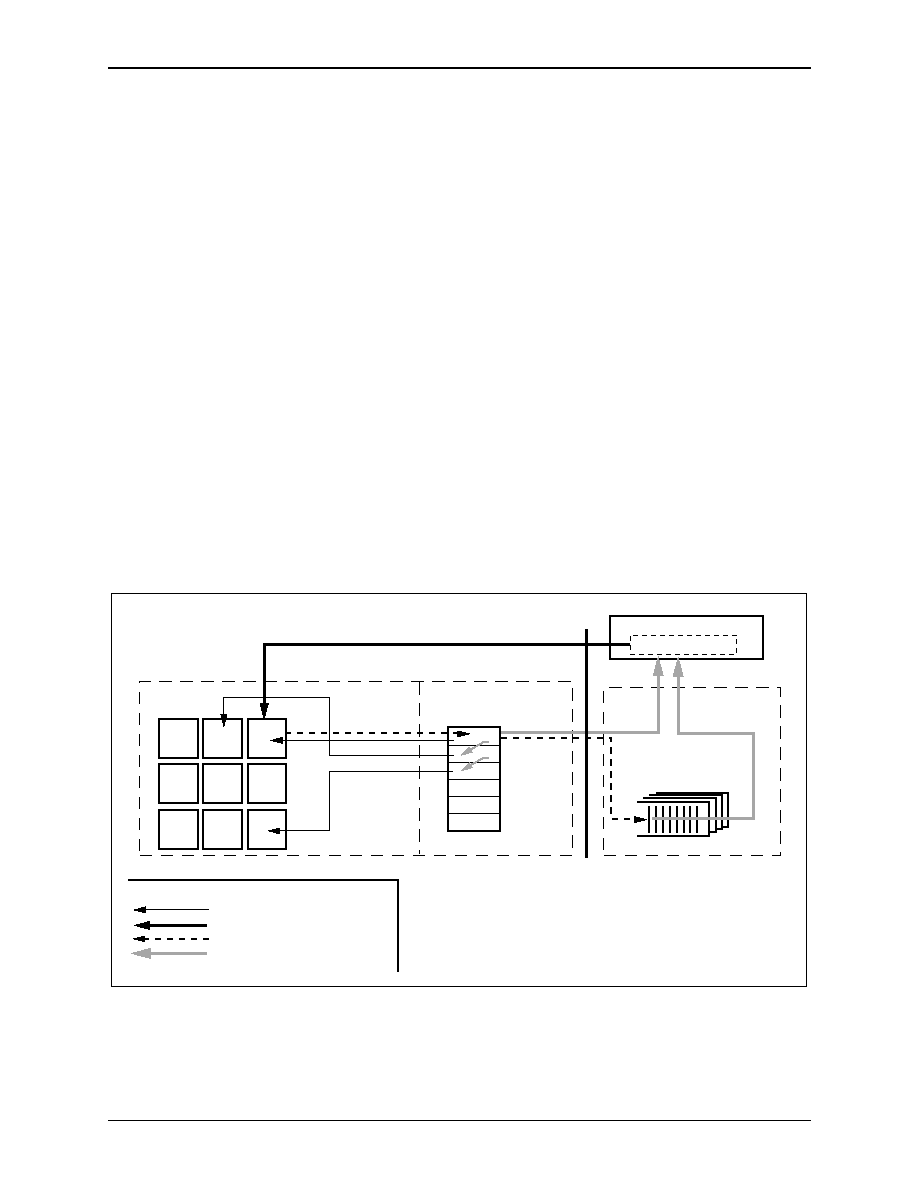
2.0 Architecture Overview
RS8234
2.2 High Performance Host Architecture with Buffer Isolation
ATM ServiceSAR Plus with xBR Traffic Management
2-6
Mindspeed Technologies
TM
28234-DSH-001-B
2.2.3 Buffer Isolation Using Descriptor-Based Buffer Chaining
The RS8234 employs buffer structures for reassembly and segmentation. The
buffer structures maximize the flexibility of the system architecture by isolating
the data buffers from the mechanisms that handle buffer allocation and linking.
This allows the data buffers to contain only payload data, no control fields or
other user fields. The user can store the data buffers separately from the buffer
descriptors and implement a minimum data copy architecture.
Figure 2-4
illustrates how reassembly data buffers and buffer descriptors are
chained together and manipulated by the ServiceSAR.
1.
The host creates a link between a reassembly data buffer and a buffer
descriptor by writing in the buffer descriptor entry, a pointer to the data
buffer.
2.
The host then formats a free buffer queue entry, which includes pointers to
both the data buffer and buffer descriptor, and writes this message to the
free buffer queue.
3.
The reassembly coprocessor reads this free buffer queue entry and uses the
pointer to the reassembly data buffer as the memory location to write the
PDU being reassembled.
4.
As reassembly of that PDU progresses, the reassembly coprocessor chains
together the necessary number of additional buffer descriptors (and thus
their associated reassembly data buffers) to complete reassembly of the PDU.
Figure 2-4. Reassembly Buffer Isolation -- Data Buffers Separated from Descriptors
(32)
Free Buffer
Queues
1
2
3
1
2
3
Data Buffers
RSM Buffer
Descriptors
Host Memory
SAR-Shared
Memory
RS8234
PCI
Host (or optionally Local) Memory
(Read)
(Write)
(Write)
(Write)
(SAR
Links
Buffer
Descriptors
for the
PDU.)
LEGEND:
RSM Coprocessor
Associations (Pointing Function)
Data Writes
Host Actions
SAR Actions
100074_005
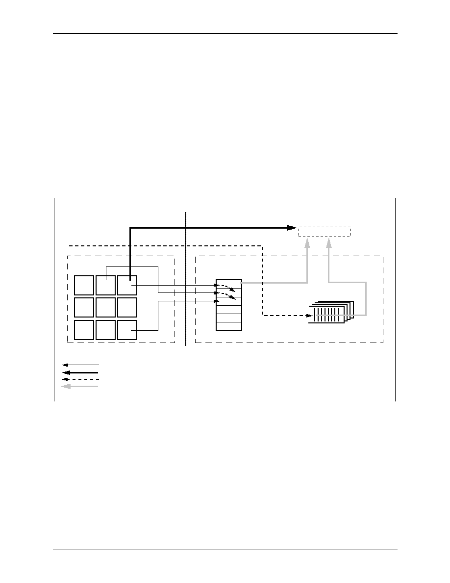
RS8234
2.0 Architecture Overview
ATM ServiceSAR Plus with xBR Traffic Management
2.2 High Performance Host Architecture with Buffer Isolation
28234-DSH-001-B
Mindspeed Technologies
TM
2-7
Figure 2-5
illustrates how the host submits linked data buffers (i.e., PDUs) to
the transmit queue for segmentation. The process is as follows:
1.
The host links the buffer descriptors (in SAR shared memory) for the
associated data buffers (in host memory) containing the PDU to be
segmented.
2.
The host then formats a two word transmit queue entry and writes this
entry to the transmit queue. The location of the first buffer descriptor in
the linked chain is contained in the transmit queue entry.
3.
The segmentation coprocessor automatically senses the presence of new
transmit queue entries, reads them, and schedules the new data for
transmission. The transmit queue acts as a FIFO for segmentation task
pointers.
Figure 2-5. Segmentation Buffer Isolation -- Data Buffers Separated from Descriptors
Transmit
Queues
1
2
3
1
2
3
Data Buffers
SEG Buffer
Descriptors
Host Memory
SEG Memory
CN8234
PCI
(Read)
(Read)
(Write)
(Write)
(Read)
SEG Coprocessor
LEGEND:
Associations (Pointing Function)
Data Reads
Host Actions
SAR Actions
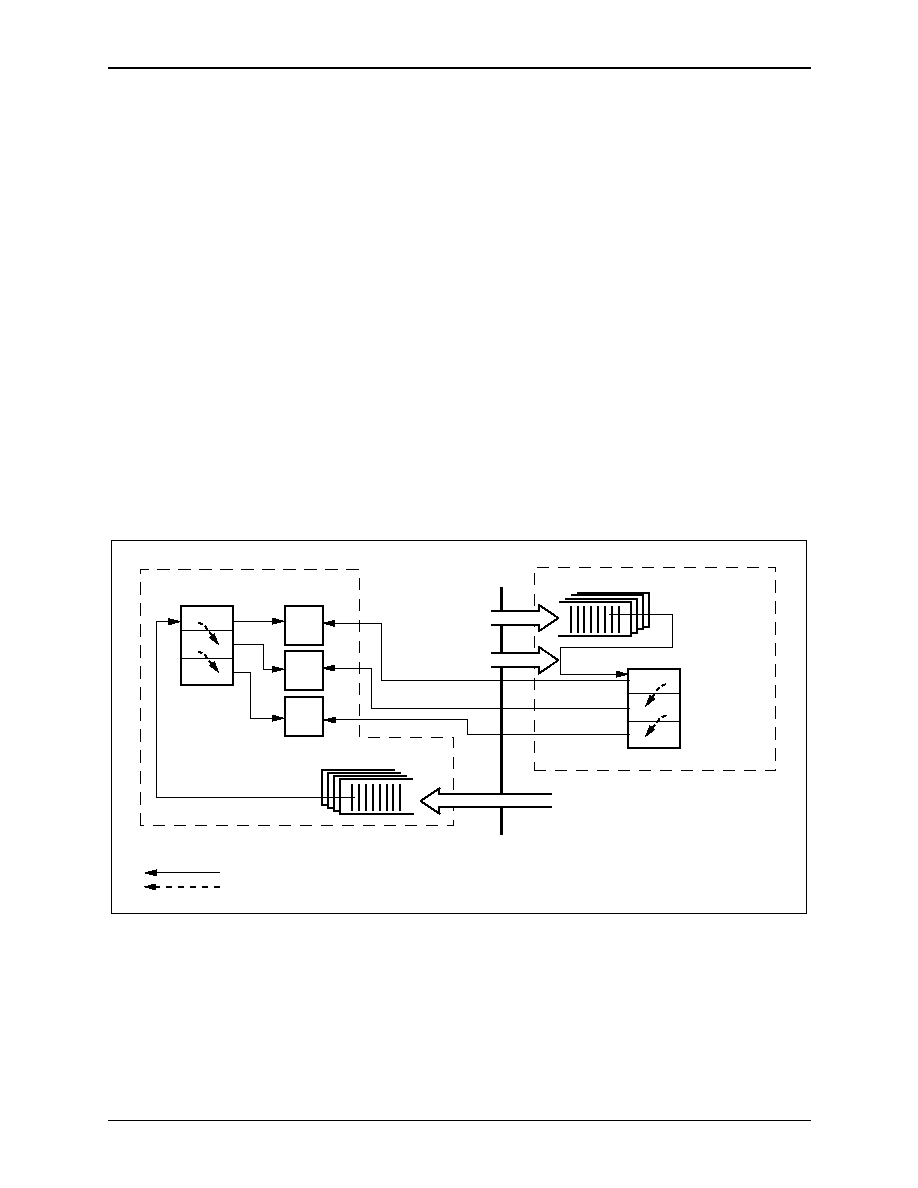
2.0 Architecture Overview
RS8234
2.2 High Performance Host Architecture with Buffer Isolation
ATM ServiceSAR Plus with xBR Traffic Management
2-8
Mindspeed Technologies
TM
28234-DSH-001-B
2.2.4 Status Queue Relation to Buffers and Descriptors
The status queues employed by the RS8234 are written by the SAR and read by
the host. These status queue entries provide the data needed by the host in order to
further process the segmentation and reassembly data flow in progress or just
completed. Each status queue entry thus includes data (such as error flags and
status bits), which the host uses in its succeeding process steps. The SAR also
includes, in each status queue entry, a pointer to the first buffer descriptor of the
segmented or reassembled data buffer(s) which comprise a single PDU. This
accomplishes the other principal function of a status queue entry: to establish the
association from the SAR to the host of the successful or unsuccessful
segmentation or reassembly of a PDU.
Figure 2-6
illustrates the association between the segmentation status queues
and segmentation data buffers and descriptors. The figure shows one three-buffer
PDU on a single virtual channel, represented by a single entry in one of the
transmit queues and a single entry in one of the SEG status queues. The host links
the buffer descriptors pointing to the data buffers containing the PDU, makes a
host-only copy of the buffer descriptor, then writes the transmit queue entry. The
SAR performs segmentation processing on the PDU and writes a SEG status
queue entry informing the host of the status of the segmentation process.
Figure 2-6. Segmentation Status Queues Related to Data Buffers and Descriptors
Transmit Queues
Host Writes
Transmit Queue
Entry
Host Writes
SBD
SAR Writes
SEG Status Queue
Entry
SEG Buffer Descriptors
SEG
Data Buffers
SEG Status Queues
Buffer Descriptors
(Host Copy)
(Buffer
Descriptors
Linked by Host)
Host Memory
PCI
SAR-Shared Memory
LEGEND:
Associations (Pointing Function)
Host Actions
8235_002

RS8234
2.0 Architecture Overview
ATM ServiceSAR Plus with xBR Traffic Management
2.2 High Performance Host Architecture with Buffer Isolation
28234-DSH-001-B
Mindspeed Technologies
TM
2-9
Figure 2-7
illustrates the association between the reassembly status queues
and reassembly data buffers and descriptors. The host submits free buffers to the
SAR by writing pointers to them in the free buffer queue entries. The SAR links
the buffer descriptors pointing to the three data buffers containing the
reassembled PDU, and writes the RSM status queue entry containing the pointer
to the first buffer descriptor for that PDU. The host further processes the PDU
utilizing that data.
Figure 2-7. Reassembly Status Queues Related to Data Buffers and Descriptors
Free Buffer Queues
Host WritesFree
Buffer Queue
Entry
SAR Writes
RSM Status Queue
Entry
RSM
Data Buffers
RSM Status Queues
RSM
Buffer Descriptors
(Buffer
Descriptors
Linked By
SAR)
Host Memory
PCI
LEGEND:
Associations (Pointing Function)
SAR Actions
SAR-Shared Memory
8235_003

2.0 Architecture Overview
RS8234
2.2 High Performance Host Architecture with Buffer Isolation
ATM ServiceSAR Plus with xBR Traffic Management
2-10
Mindspeed Technologies
TM
28234-DSH-001-B
2.2.5 Write-Only Control/Status
Figure 2-8
illustrates the RS8234's write-only PCI control architecture. The host
manages the RS8234 ATM terminal using write-only control and status queues.
This architecture minimizes PCI bus utilization by eliminating reads from control
activities. PCI writes utilize the bus much more efficiently than PCI reads. During
a PCI write, the Bus Master can post the write data to an internal FIFO in the
slave, terminate the transaction, and immediately release the bus. On the other
hand, during PCI reads, the Bus Master retrieves the data from the slave while
holding the bus. Since the data retrieval takes some time, reads increase the PCI
bus utilization time for each transaction. The RS8234 eliminates read operations
except for burst reads to gather segmentation data.
2.2.6 Scatter/Gather DMA
The RS8234's Direct Memory Access (DMA) coprocessor works in close
conjunction with the segmentation and reassembly coprocessors to gain access to
the PCI bus, transfer the requested data, and notify the segmentation or
reassembly coprocessor that the transfer is complete. The DMA coprocessor
transfers all data using the read and write burst buffers in the PCI Bus Interface.
In general, two types of transactions are processed: 12- or 14-word burst
accesses for data, or 1- to 4-word accesses for control and status messages.
For outgoing messages, the DMA coprocessor moves data from host memory
to the segmentation coprocessor using a gather DMA method. For incoming
messages, the DMA coprocessor moves data from the reassembly coprocessor to
host memory using a scatter DMA method.
The DMA coprocessor is capable of handling transfers from the PCI bus with
data that is not aligned on word boundaries. It will also selectively transfer data to
comply with either a big endian or little endian host data structure.
Figure 2-8. Write-Only Control and Status Architecture
Write-only architecture reduces PCI utilization dramatically,
as reads take many more clock cycles.
Control
RSM Data (Writes)
Status
SEG Data (Read Multiples)
Host
RS8234
PCI
100074_009

RS8234
2.0 Architecture Overview
ATM ServiceSAR Plus with xBR Traffic Management
2.2 High Performance Host Architecture with Buffer Isolation
28234-DSH-001-B
Mindspeed Technologies
TM
2-11
2.2.7 Interrupts
The RS8234 informs the host of segmentation and reassembly activity by means
of maskable interrupts sent to the host processor, triggered by writes to the
segmentation and reassembly status queues.
The user can configure the SAR to generate these status queue entries and
interrupts at PDU boundaries (called Message Mode), or at data buffer
boundaries (called Streaming Mode).
The RS8234 can also be configured with a status queue interrupt delay, which
can be enabled in order to reduce the interrupt processing load on the host. This
has value when the SAR resides in an environment in which the host is not
dedicated to datacom processing.

2.0 Architecture Overview
RS8234
2.3 Automated Segmentation Engine
ATM ServiceSAR Plus with xBR Traffic Management
2-12
Mindspeed Technologies
TM
28234-DSH-001-B
2.3 Automated Segmentation Engine
The RS8234 can segment up to 64 K VCCs simultaneously. The segmentation
coprocessor block independently segments each channel and multiplexes the
VCCs onto the line with cell level interleaving. For each cell transmission
opportunity, the xBR Traffic Manager tells the segmentation coprocessor which
VCC to send.
The RS8234 provides full support of the AAL5 and AAL3/4 protocols and a
transparent or NULL adaptation layer, AAL0.
Each segmentation channel is specified as a single entry in the segmentation
VCC Table located in SAR shared memory. A VCC specifies a single VC or VP
in the ATM network. These VCC Table entries define the negotiated or contracted
characteristics of the traffic for that channel, and are initialized by the host either
during system initialization or on-the-fly during operation. An initialized
segmentation VCC Table entry effectively establishes a connection on which data
can be segmented.
NOTE:
ABR VCCs occupy two table entries.
The host submits data for segmentation by first linking buffer descriptors that
point to the buffers containing the PDU to be transmitted, and then submitting
that chained message to the SAR by writing to one of 32 independent circular
transmit queues.
The segmentation coprocessor then operates autonomously, formatting the
cells on each channel according to the host-defined segmentation VCC Table
entries for each channel. The formatting functions include the following:
�
The segmentation coprocessor formats the ATM cell header for each cell,
based on the settings in the segmentation VCC Table entry for that VCC.
�
The segmentation coprocessor also generates the CPCS-PDU header and
trailer fields in the first and last cell of the segmented PDU.
�
For AAL5 traffic, the SEG coprocessor also generates the PDU-specific
fields in the trailer of the CPCS-PDU, and places these in the last cell (the
End of Message [EOM] cell) for the PDU.
�
Each AAL3/4 cell carries 44 octets of payload and four octets (in five
fields) of header and trailer information. The SAR performs the formatting
steps necessary to create AAL3/4 cells.
�
AAL0 is intended for client-proprietary use. For AAL0, the segmentation
coprocessor segments the Service Data Unit (SDU) to ATM cell payload
boundaries and generates ATM cell headers, but generates no other
overhead fields.
�
The user has per-channel, per-PDU control of Raw Cell Mode
segmentation, wherein the segmentation coprocessor reads the entire
52-octet ATM cell from the segmentation buffer and does not generate the
ATM headers for the cells.
�
The formatted cells are passed through the transmit FIFO to the PHY
interface for transmission.

RS8234
2.0 Architecture Overview
ATM ServiceSAR Plus with xBR Traffic Management
2.3 Automated Segmentation Engine
28234-DSH-001-B
Mindspeed Technologies
TM
2-13
The system designer can set the depth of the transmit FIFO from one to nine
cells deep in order to optimize the balance between Cell Delay Variation (CDV)
(which increases with longer transmit FIFO depth) and PCI latency protection
(which decreases with shorter transmit FIFO depth).
The RS8234 provides a method to segment traffic from a fixed PCI address
(or Virtual FIFO). This is intended for circuit-based CBR traffic such as voice
channel(s).
The RS8234 reports segmentation status to the host on one of a set of 32
independent parallel segmentation status queues. The RS8234 writes
segmentation status queue entries on either PDU boundaries or buffer boundaries,
selectable on a per-VCC basis. PDU boundary status reporting is called Message
Mode, while buffer status reporting is called Streaming Mode.

2.0 Architecture Overview
RS8234
2.4 Automated Reassembly Engine
ATM ServiceSAR Plus with xBR Traffic Management
2-14
Mindspeed Technologies
TM
28234-DSH-001-B
2.4 Automated Reassembly Engine
The reassembly coprocessor processes cells received from the ATM Physical
Interface block. The coprocessor extracts the AAL SDU payload from the
received cell stream and reassembles this information into buffers supplied by the
host system.
Each active reassembly channel is specified as a single entry in the reassembly
VCC Table located in SAR shared memory. One RSM VCC Table entry defines
the negotiated or contracted characteristics of the reassembly traffic for a
particular channel. Each table entry is initialized by the host during system
initialization, or on-the-fly. The SAR uses the RSM VCC Table to store
temporary information to assist the reassembly process. An initialized
Reassembly VCC Table entry effectively establishes a connection on which the
RS8234 can reassemble data.
Using a dynamic Channel Directory lookup method, the RS8234 reassembles
up to 64 K VCCs simultaneously at a maximum rate of 200 Mbps on simplex
connections and 155 Mbps on full duplex connections. The Channel Directory
mechanism allows flexible preallocation of resources and provides deterministic
channel identification over the full UNI or NNI Virtual Path Identifier/Virtual
Channel Identifier (VPI/VCI) address space. The total number of VCCs
supported is limited by the memory allocated to the RSM VCC Table and the
Channel Directory.
The reassembly coprocessor extracts the AAL SDU payload from the received
cell stream and reassembles this information into system buffers allocated
per-VCC. The RS8234 supports AAL5, AAL3/4 and AAL0 reassembly, as well
as 52-octet Raw Cell mode.
For AAL5, the reassembly coprocessor extracts and checks all PDU protocol
overhead.
For AAL3/4, the reassembly coprocessor performs all error detection and
checking procedures incorporated in AAL3/4, and reassembles SDUs based on
Message ID (MID).
The RS8234 provides two methods of terminating an AAL0 PDU:
1.
Payload Type Identifier (PTI) termination, wherein the PTI bit in the cell
header is monitored for the End of Message (EOM) cell indication
2.
Cell Count termination, wherein the RS8234 terminates the PDU when a
user-defined number of cells have been received on that channel
The AAL0 PDU termination method is selectable on a per-VCC basis.
The user can, on a per-channel basis, establish Raw Cell mode reassembly. In
this mode the Header Error Check (HEC) octet is deleted to align the 53-octet cell
to 32-bit boundaries, and the RSM coprocessor reassembles the entire 52-octet
ATM cell into the reassembly buffer.

RS8234
2.0 Architecture Overview
ATM ServiceSAR Plus with xBR Traffic Management
2.4 Automated Reassembly Engine
28234-DSH-001-B
Mindspeed Technologies
TM
2-15
The RS8234 provides the user with generous per-channel control of the
reassembly process, including the following:
�
Assignment of priorities for reassembly buffer return processing
�
Cell filtering on inactive channels
�
Mechanisms to establish per-VCC firewalling by allocating buffer credits
on a per-channel basis. (This limits the possibility of one VCC consuming
all of the memory resources.)
�
Per-VCC activation and control of a background hardware time-out
function where the user selects one of eight programmable time-out
periods. (The background function then automatically detects partially
reassembled PDUs and reports this status to the host so that these buffers
can be recovered and re-allocated.)
�
Per-VCC monitoring of the length of the reassembled PDU, with status
reporting if the length exceeds a set maximum length for that channel
The RS8234 implements an early packet discard feature to enable discarding
of complete or partial CPCS-PDUs based upon service discard attributes or error
conditions. The early packet discard function halts reassembly of the CPCS-PDU
marked for discard until the next Beginning of Message (BOM) cell and/or the
error condition has cleared. The SAR writes a status queue entry with the
appropriate status flags set, which indicate the reason for the discard. This
function can be enabled for the following conditions:
�
Frame Relay discard based on the frame's DE setting and the channel
exceeding a user-defined priority threshold
�
CLP packet discard based on the received cell's CLP bit setting and
exceeding channel priority threshold
�
LANE-LECID packet discard on ELAN channels, which implements echo
suppression on multicast data frames
�
Early packet discard on AAL5 channels when the reassembled PDU length
exceeds the user-defined maximum PDU length for that VCC
�
Early packet discard on channels encountering a free buffer queue empty
(underflow) condition (meaning there are no available buffers in the free
buffer queue that channel is assigned to)
�
Early packet discard on PDUs when a DMA Incoming FIFO Full condition
occurs
�
Early packet discard on channels encountering a reassembly status queue
full (overflow) condition
�
Early packet discard on AAL3/4 channels with these MIB errors: ST_ERR
(Segment Type error), SN_ERR (Sequence Number error), and LI_ERR
(SAR-PDU Length error)
The system designer can set the reassembly status reporting for any channel to
either Message Mode or Streaming Mode. In Message Mode, a status entry is
written only when the last buffer in a message completes reassembly. In
Streaming Mode, a status entry is written for each buffer as it completes
reassembly.

2.0 Architecture Overview
RS8234
2.5 Advanced xBR Traffic Management
ATM ServiceSAR Plus with xBR Traffic Management
2-16
Mindspeed Technologies
TM
28234-DSH-001-B
2.5 Advanced xBR Traffic Management
The RS8234 implements ATM's inherent robust traffic management capabilities
for CBR, VBR, ABR, UBR, GFR and GFC. The RS8234 manages each VCC
independently and dynamically.
�
The user assigns each connection a service class, a priority level, and a rate if
applicable. Then, the on-chip traffic controller, the xBR Traffic Manager,
optimizes usage of the line bandwidth according to the VCC's traffic
parameters and control information stored in SAR shared memory. The xBR
Traffic Manager guarantees the compliance of each VCC to its service
contract with the ATM network at the UNI ingress point. It schedules all data
traffic by acting as a master to the segmentation coprocessor.
One of the functional components of the xBR Traffic Manager is the
xBR Scheduler. The xBR Traffic Manager assigns segmentation traffic
from active VCCs to schedule `slots', which the segmentation coprocessor
then complies to by segmenting VCC traffic in the sequence/schedule dic-
tated by the xBR Scheduler.
�
In addition to reserved CBR bandwidth, the RS8234 provides 16
segmentation priorities. The user configures these priorities for the
remaining service categories, including the TM 4.1 defined ABR class.
The RS8234's xBR Traffic Manager implements multiple functional
levels of traffic prioritizing. This is illustrated in
Figure 2-9
.
�
The host submits data to be sent by writing entries to the transmit queues
for segmentation. The SAR processes these transmit queues either in round
robin order (transmit queue zero through thirty-one, looped back to zero),
or in priority order (with transmit queue thirty-one having highest
priority). This scheme gives the user or system designer some control of
the delay between the host submitting traffic and the SAR starting to
process that traffic. For instance, the user could assign CBR traffic to the
highest priority transmit queue in order to minimize any delay in
processing and scheduling that traffic.
�
The RS8234 then submits this traffic demand to the xBR Traffic Manager
for scheduling. Traffic is scheduled based on the traffic class plus certain
parameters from the segmentation VCC Table entries (primarily the GCRA
I and L parameters). And if the service category is ABR, the SAR also uses
certain parameters from the ABR templates to help determine that traffic's
placement on the Schedule Table.
�
The conforming traffic to be transmitted is further groomed in internal
priority queues. Each virtual channel is prioritized according to its
assigned scheduling priority. CBR channels are given pre-assigned
segmentation bandwidth, and channels for the remaining service
categories scheduled according to their priority number (priority zero
being the lowest priority and priority fifteen being highest).
Figure 2-9
shows this prioritization as a global set of queues, but it is actually
maintained on a per-transmit opportunity basis. In this way, high priority
traffic will be transmitted up to its GCRA limits but will not block lower
priority traffic when idle.
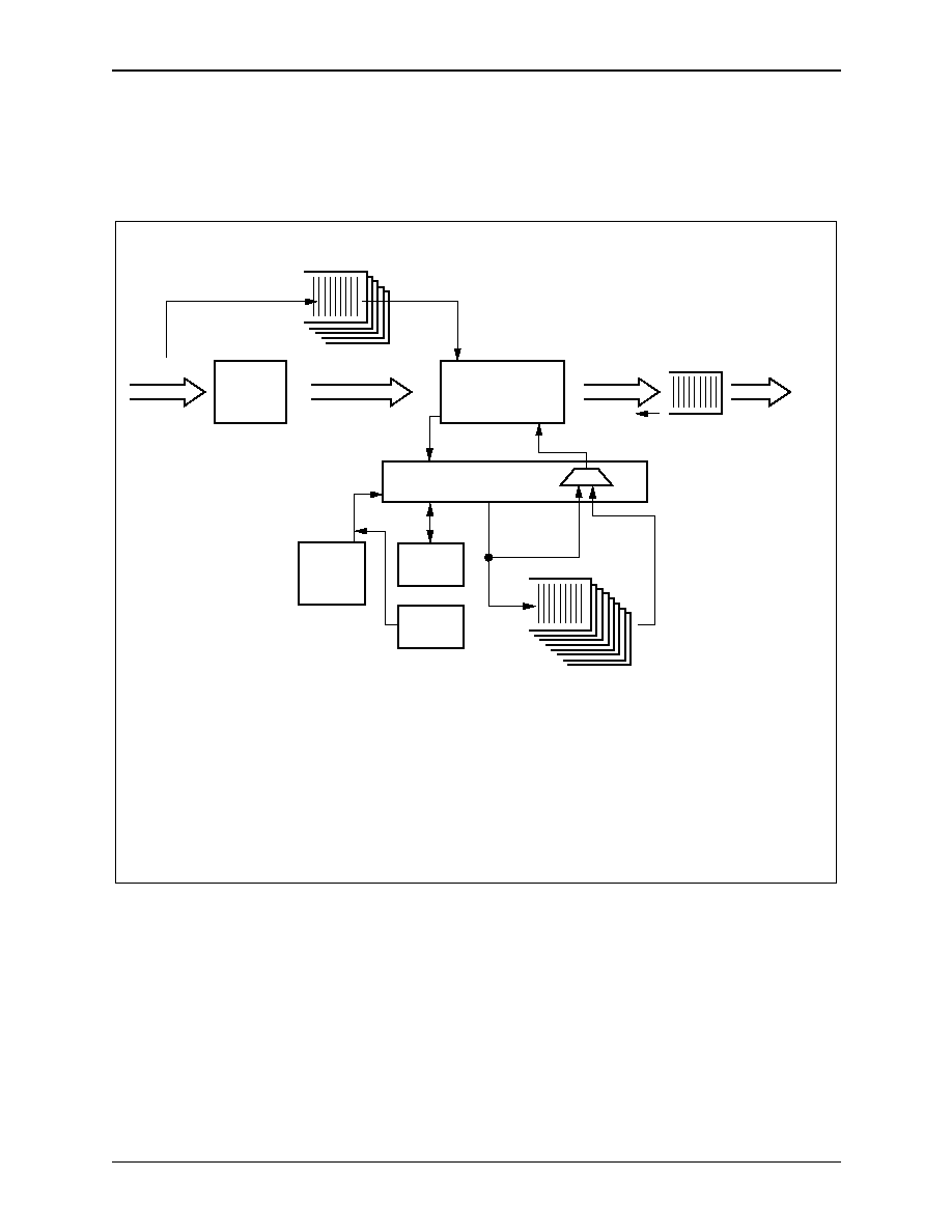
RS8234
2.0 Architecture Overview
ATM ServiceSAR Plus with xBR Traffic Management
2.5 Advanced xBR Traffic Management
28234-DSH-001-B
Mindspeed Technologies
TM
2-17
The RS8234 asynchronously multiplexes traffic based on the above
schemes, as the Tx FIFO empties.
Figure 2-9. Multi-Level Model for Prioritizing Segmentation Traffic
(1)
(1)
(2)
(2)
(3)
(3)
(5)
(5)
(4)
(4)
Host
SAR
To
PHY
Data
Buffers
Transmit Queues
(32)
Segmentation
Coprocessor
Tx FIFO
Buffer
Full/Empty
Start
Next Tx VCC ID #
Traffic
Parameters
Conforming
VCC ID #
UBR/VBR/ABR
VCC ID #
CBR
xBR Traffic
Manager
VCC
Control
Tables
Schedule
Table
ABR
Templates
16 UBR/VBR/ABR
Priority Queues
The user initializes traffic parameters on a per-VCC basis.
User selects priority or round-robin service policy on transmit queues.
The segmentation coprocessor notifies the Traffic Manager when a VCC becomes active, through
reading new entries from the transmit queue.
Each conforming non-CBR VCC is assigned to a priority queue, while conforming CBR VCCs
are simply slated for transmit.
The highest priority conforming cell is formatted and put on the Tx FIFO buffer for transmit.
NOTE(S):
100074_010

2.0 Architecture Overview
RS8234
2.5 Advanced xBR Traffic Management
ATM ServiceSAR Plus with xBR Traffic Management
2-18
Mindspeed Technologies
TM
28234-DSH-001-B
2.5.1 CBR Traffic
The CBR service category requires guaranteed transmission rates, as well as
constrained CDV. The RS8234 facilitates these needs when generating CBR
traffic by pre-assigning specific schedule slots to CBR VCCs. For each CBR
assigned cell slot, the RS8234 generates a cell for that specific VCC unless data is
not available. The RS8234 also minimizes CDV by basing all traffic management
on a local reference clock.
The RS8234 provides a mechanism to exactly match the scheduled rate of a
CBR channel to the rate of its data source. The host may occasionally instruct the
xBR Scheduler to skip one transmit opportunity on a channel in order to
accomplish this rate-matching.
The RS8234 manages CBR tunnels in the same manner as a CBR VCC.
However, instead of one VCC, several UBR, VBR or ABR VCCs can be
scheduled within this CBR tunnel, in round-robin order.
Unused CBR and Tunnel time slots are automatically made available to VCCs
of other service categories by the xBR Scheduler.
2.5.2 VBR Traffic
The RS8234 takes advantage of the asynchronous nature of ATM by reserving
bandwidth for VBR channels at average cell transmission rates without
pre-assigning "hardcoded" schedule slots, as with CBR traffic. This dynamic
scheduling allows VBR traffic to be statistically multiplexed onto the ATM line,
resulting in better utilization of the shared bandwidth resources. The xBR
Scheduler supports multiple priority levels for VBR traffic. Through the
combination of VBR parameters and priorities, it is possible to support real-time
VBR services.
The outgoing cell stream for each VBR VCC is scheduled according to the
GCRA algorithm. The GCRA I and L parameters control the per-VCC Peak Cell
Rate (PCR) and Cell Delay Variation Tolerance (CDVT) of the outgoing cell
stream on any channel. This guarantees compliance to policing algorithms
applied at the network ingress point. The user can control the granularity of rate
by dictating the number of schedule slots in the schedule table.
Channels can be rate-shaped as VCs or VPs according to one of three VBR
definitions. VBR1 controls PCR and CDVT. VBR2 controls PCR and CDVT, as
well as Sustained Cell Rate (SCR) and Burst Tolerance (BT). VBRC (also called
VBR3) controls PCR and CDVT on all cells, but controls SCR on only CLP = 0
(i.e., high priority) cells.

RS8234
2.0 Architecture Overview
ATM ServiceSAR Plus with xBR Traffic Management
2.5 Advanced xBR Traffic Management
28234-DSH-001-B
Mindspeed Technologies
TM
2-19
2.5.3 ABR Traffic
The RS8234 implements the ATM Forum ABR flow control algorithms. The
RS8234 acts as both a fully compliant ABR Source and Destination, as defined in
the TM 4.1 specification. The ABR service category effectively allows low cell
loss transmission through the ATM network by regulating transmission based
upon network feedback. The ABR algorithms regulate the rate of each VCC
independently.
The RS8234 employs an internal feedback control loop mechanism to enable
the TM 4.1 ATM Source specification. The SAR utilizes the dynamic rate
adjustment capability of the xBR Scheduler as the ATM Source's variable traffic
rate shaper. The RS8234 injects an in-rate stream of Forward RM cells for each
ABR VCC. When these cells return to the RS8234's receive port as Backward
RM cells after a round trip through the network, the RS8234 processes these cells
and uses the data returned as feedback to dynamically adjust the rates on each
ABR channel.
The RS8234 also responds to an incoming ABR cell stream as an ABR
Destination. The reassembly coprocessor processes received Forward RM cells. It
"turns around" this incoming information to the segmentation coprocessor, which
formats Backward RM cells containing this information, and inserts these
Turnaround RM cells into the transmit cell stream.
The exact performance of the rate-shaper is governed by one or more ABR
Templates in SAR shared memory. Each VCC is assigned to one of these
templates. The templates control such behaviors as the size of the additive rate
increase factors or multiplicative rate decrease steps. Each VCC's rate varies
across the template independently.
2.5.4 UBR Traffic
The UBR service category is intended for non-real-time applications that do not
require tightly constrained delay and delay variation, such as traditional computer
communications applications like file transfer and e-mail.
Those VCCs which have not been assigned to one of the other service
categories covered previously are scheduled as UBR traffic. All UBR channels
within a priority are scheduled on a round-robin basis. To limit the bandwidth that
a UBR priority consumes, the system designer should use a CBR tunnel in that
priority level.
2.5.5 GFR Traffic
Guaranteed Frame Rate is a new service category defined by the ATM Forum to
provide a MCR QoS guarantee for AAL5 CPCS-PDUs not exceeding a specified
frame length. A GFR service connection is treated as UBR with a guaranteed
MCR.
The RS8234 implements GFR by scheduling/shaping the connections using
both the VBR1 scheduling procedure (for the MCR rate value) and a UBR
priority queue, thereby providing fair sharing for all GFR connections to excess
bandwidth.

2.0 Architecture Overview
RS8234
2.5 Advanced xBR Traffic Management
ATM ServiceSAR Plus with xBR Traffic Management
2-20
Mindspeed Technologies
TM
28234-DSH-001-B
2.5.6 xBR Cell Scheduler
The xBR Scheduler slates traffic for transmission according to a Dynamic
Schedule Table maintained in SAR shared memory. The table contains a
user-programmable number of schedule slots. The duration of a single slot is a
user-programmable number of system clock cycles. The xBR Scheduler
sequences through this table in a circular fashion to schedule traffic. By
configuring the number of slots in the table and the duration of each slot, the
system designer chooses a range of available rates. A specific rate for any channel
is determined by how many slots in the table to which that channel is assigned.
Schedule slots not reserved for CBR during table setup are used for the rest of the
service categories.
The xBR Scheduler implements Mindspeed's proprietary per-VCC rate
shaping algorithms. The predecessor to the RS8234, the Bt8230 SAR, proved the
core algorithms. The RS8234 extends their use to other service classes. The
RS8234 xBR Scheduler shapes all traffic classes, including CBR, single leaky
bucket VBR, dual leaky bucket VBR, ABR, and UBR. The host configures the
Dynamic Schedule Table during system initialization, defining the table size in
number of schedule slots and the length of each schedule slot in clock cycles.
After setup, the RS8234 dynamically manages the entire table.
Some key features of the xBR Scheduler are:
1.
Per-VCC rate control guarantees conformance to GCRA UPC/policing
2.
Dynamic reallocation of link bandwidth to active channels
3.
Dynamic, fair sharing of bandwidth on oversubscribed lines
4.
Multiple scheduling priorities
5.
Fine grained rate control
6.
Rate based on a user supplied reference clock
Dynamic management provides on-the-fly reallocation of link bandwidth
without host intervention. The RS8234 fairly distributes the link bandwidth to
channels based upon their QoS parameters and assigned transmission priority. As
covered previously, the RS8234 supports 16 priorities in addition to preallocated
CBR time slots.
The xBR Scheduler facilitates advanced network traffic management
topologies. The RS8234 rate shapes VCs or VPs. Additionally, CBR tunneling
allows UBR, VBR and/or ABR traffic management schemes to operate under a
preallocated CBR limit.

RS8234
2.0 Architecture Overview
ATM ServiceSAR Plus with xBR Traffic Management
2.5 Advanced xBR Traffic Management
28234-DSH-001-B
Mindspeed Technologies
TM
2-21
2.5.7 ABR Flow Control Manager
The ABR Flow Control Manager operates in conjunction with the xBR Scheduler
to control the rate of ABR channels. The RS8234 implements the TM 4.1
specification in a template-controlled hardware state machine. Mindspeed
provides an initial set of templates which reside in SAR shared memory. The
information within these templates define conformant ABR behavioral responses
to network and connection states. The RS8234 generates ABR Source traffic,
including internally generated RM cells, according to the template instructions.
The reassembly coprocessor and the Flow Control Manager collaboratively act as
a fully compliant ABR Destination Terminal.
These templates provide three significant benefits to the user:
1.
Since they control the Flow Control Manager state machine, they can be
optimized for specific applications.
2.
The programmability of the templates insulates the hardware from changes
in the TM 4.1 specification.
3.
Mindspeed provides the initial templates, which may be customized by the
user later, which shortens developmen
t t
ime.
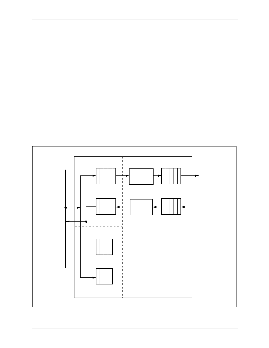
2.0 Architecture Overview
RS8234
2.6 Burst FIFO Buffers
ATM ServiceSAR Plus with xBR Traffic Management
2-22
Mindspeed Technologies
TM
28234-DSH-001-B
2.6 Burst FIFO Buffers
To conserve local memory bandwidth, the RS8234 does not use its local SRAM
as a buffer for incoming or outgoing data. Instead, the RS8234 uses six dedicated
internal FIFO data buffers as follows:
�
Two DMA master burst FIFO buffers (read =16 words; write=512 words.
�
Two DMA slave burst FIFO buffers, (read = 8 words and write = 64
words).
�
One FIFO buffer between the PHY interface and the segmentation coprocessor
(
1 to 9 cells)
. See
Section 4.2.4
.
�
One FIFO buffer between the PHY interface and the reassembly
coprocessor (64 words).
Figure 2-10
illustrates the data FIFO buffer.
Figure 2-10. Data FIFO Buffers
PCI
PCI Master
PCI Slave
PHY
Interface
16
512
8
64
1 to 9 Cells
64
DMA Master Read
Burst FIFO Buffer
DMA Slave Read
Burst FIFO Buffer
DMA Slave Write
Command +
Data FIFO Buffer
DMA Master Write
Burst FIFO Buffer
Transmit PHY
Interface FIFO
Receive PHY
Interface FIFO
Segmentation
Controller
Reassembly
Controller
8236_097

RS8234
2.0 Architecture Overview
ATM ServiceSAR Plus with xBR Traffic Management
2.7 Implementation of OAM-PM Protocols
28234-DSH-001-B
Mindspeed Technologies
TM
2-23
2.7 Implementation of OAM-PM Protocols
The RS8234 provides internal support for the detection and generation of OAM
traffic, including PM OAM.
The RS8234 supports the F4 and F5 OAM flows according to I.610. It
monitors up to 128 channels and generates in-rate PM-OAM cells.
The RS8234 includes a Local Processor Interface, providing the capability of
SAR shared memory segmentation and reassembly. The user can thus route OAM
traffic, including PM traffic, to and from this optional local processor, thereby
off-loading ATM network management from the host. To facilitate this, the
RS8234 provides the option of user-defined global status queues for both
segmentation and reassembly and a global buffer queue for reassembly, to which
the user can assign SAR shared memory addresses. The RS8234 will then process
OAM traffic via the local processor, thereby isolating the host from these
management functions and focusing host processing power on ATM user data
traffic.

2.0 Architecture Overview
RS8234
2.8 Standards-Based I/O
ATM ServiceSAR Plus with xBR Traffic Management
2-24
Mindspeed Technologies
TM
28234-DSH-001-B
2.8 Standards-Based I/O
PCI Bus I/O
The PCI bus interface implements the full set of address, data, and control signals
required to drive the PCI bus as a master, and contains the logic required to
support arbitration for the PCI bus. This interface is PCI Version 2.1 compliant.
The PCI bus interface also includes an interface module that allows the PCI
core to connect to a serial EEPROM. This 128-byte EEPROM is used to store
specific PCI configuration information, loaded into the PCI Configuration space
at reset. This allows several user-configurable features:
�
User control of the size of the memory block for PCI addresses
�
Enabling byte swapping of control words across the PCI bus
�
Loading of Subsystem ID and Subsystem Vendor ID
ATM PHY I/O
The RS8234's ATM physical interface communicates with and controls the ATM
link interface device, which carries out all the transmission convergence and
physical media dependent functions defined by the ATM protocol. Two modes of
operation are provided: standard UTOPIA and slave UTOPIA. Standard UTOPIA
mode conforms to the UTOPIA Level 1 standard for an ATM Layer device. Slave
UTOPIA mode reverses the control direction for use in place of a PHY on switch
fabrics.
SAR Shared Memory I/O
To simplify system implementations, the RS8234 integrates a complete memory
controller designed for direct interface to common Static RAMs (SRAMs). The
RS8234's memory controller operates at 33 MHz and can access up to 8 MB of
SRAM memory. The memory controller also arbitrates access to the internal
control and status registers by the host and local processors. The memory banks
can be configured to a variable number of sizes. All of this affords a wide degree
of flexibility in SAR shared memory architecture.
Local Processor I/O
The Local Processor Interface in the RS8234 allows an optional external CPU to
be directly connected to the device to serve as a local controlling intelligence that
can handle initialization, connection management, overall data management,
error recovery, and OAM functions. The use of a local processor for these
functions allows ATM message data to flow to and from host system memory in a
substantially larger bandwidth, as the local processor is handling the "out of
band" functions described above.
The processor interface is "loosely coupled," meaning that the processor
connects to the RS8234 through bidirectional transceivers and buffers for the
address and data buses. This allows the processor fast access to RS8234 memory
and registers, but insulates the RS8234 from processor instruction and data cache
fills. It also allows the processor to control multiple RS8234s or physical devices
if desired.

RS8234
2.0 Architecture Overview
ATM ServiceSAR Plus with xBR Traffic Management
2.9 Electrical/Mechanical
28234-DSH-001-B
Mindspeed Technologies
TM
2-25
Boundary Scan I/O and Loopbacks
The RS8234 includes five pins for Joint Test Action Group (JTAG) Boundary
Scan, for board-level testing. The RS8234 incorporates an internal loopback from
the segmentation coprocessor to the reassembly coprocessor, to facilitate system
diagnostics.
2.9 Electrical/Mechanical
The RS8234 is a CMOS device packaged in a 388 Ball Gate Array (BGA) format.
It operates from a 3.3V power supply and within the standard industrial
temperature range.
The device inputs are tolerant of 5 V signal levels, so external 5 V devices
may be used. Any I/O (except PCI) that requires a pullup must be tied through a
resistor to 3.3 V and not 5 V.
2.10 Logic Diagram and Pin Descriptions
A functionally partitioned logic diagram of the RS8234 is shown in Figure 2-11.
Pin descriptions, names and input/output assignments are detailed in
Table 2-1
.
2.0 Architecture Overview
RS8234
2.10 Logic Diagram and Pin Descriptions
ATM ServiceSAR Plus with xBR Traffic Management
2-26
Mindspeed Technologies
TM
28234-DSH-001-B
Figure 2-11. RS8234 Logic Diagram (1 of 3)
HAD31
HC/BE3*
HPAR
HFRAME*
HIRDY*
HTRDY*
HSTOP*
HDEVSEL*
HIDSEL
HGNT*
HPERR*
HSERR*
HCLK
HRST*
HREQ*
HINT*
PCI Interface
Signals
I/O
I/O
I/O
I/O
I/O
I/O
I/O
I/O
I
I
I/O
OD
I
I
O
OD
Address/Data Bus
Command/Byte Enable
Address/Data Command Parity
Framing Signal
Transactor Initiator Ready
Transaction Target Ready
Transaction Termination
Bus Device Acknowledge
Bus Device Slot Select
Bus Grant
Bus Parity Error
System Error
Bus Clock
System Reset
Arbiter Bus Request
Interrupt Request
Host
Y26
AA25
L23
HLED*
OD LED Power
L4
HENUM*
OD ENUM#
B23
W24
HAD30
HAD29
HAD28
HAD27
HAD26
HAD25
HAD24
HAD23
HAD22
HAD21
HAD20
HAD19
HAD18
HAD17
HAD16
HAD15
HAD14
HAD13
HAD12
W25
W26
V24
V25
V26
U23
U24
T25
R23
R24
R25
R26
P24
P25
P26
J26
J25
J24
H25
HAD11
HAD10
HAD9
HAD8
HAD7
HAD6
HAD5
HAD4
HAD3
HAD2
HAD1
HAD0
HC/BE2*
HC/BE1*
HC/BE0*
H24
H23
G26
G25
F25
F24
F23
E26
E23
D26
D25
D24
T23
N26
K23
F26
K24
M25
M24
M23
L25
L26
T24
Y25
L24
N23
Y23
PCI5V
AB26
I
Bus Signalling
I
100074
I = Input, O = Output, OD = Open Drain Output
The symbol (*) Indicates Active Low

RS8234
2.0 Architecture Overview
ATM ServiceSAR Plus with xBR Traffic Management
2.10 Logic Diagram and Pin Descriptions
28234-DSH-001-B
Mindspeed Technologies
TM
2-27
RS8234 Logic Diagram (2 of 3)
TXD7
TXSOC(TXMARK)
TXCLAV(TXFLAG*)
TXEN*
RXPAR
RXSOC(RXMARK)
RXCLAV(RXFLAG*)
RXEN*
RXCLK(FRCTRL)
ATM Physical
Interface
I/O
I/O
I/O
I
I
I
I/O
I/O
I
O
Transmit Cell Marker
Transmit Flag
Transmit Enable
Receive Data
Receive Data Parity
Receive Cell Marker
Receive Flag
Receive Enable
Framer Control/Clock
Transmit Data
O
Transmit Data Parity
I = Input, O = Output, OD = Open Drain Output
Framer Configuration
I
FRCFG1
The symbol (*) Indicates Active Low
FRCFG0
AF12
AE12
TXD6
TXD5
TXD4
TXD3
TXD2
TXD1
TXD0
AF15
AF16
AC14
AD5
AC10
AE11
AD10
AC13
AF19
AE19
AF20
AE20
AD20
AC20
AF21
AE21
TXPAR
AE16
RXD7
RXD6
RXD5
RXD4
RXD3
RXD2
RXD1
RXD0
AC8
AD8
AE8
AF8
AC9
AF9
Framer Configuration
I
PADDR1
PBSEL1
PBE3*
PCS* (PHYCS1*)
PAS*
PBLAST* (PHYCS2*)
PWAIT*
PWNR
PFAIL*
PRDY*
PDAEN*
Local Bus
Processor
I
I
I
I/O
I/O
I/O
I
I/O
I
O
I/O
Word Select
Bank Select
Write Byte-Enables
SAR/ATM Chip Select
Address Strobe
Burst Last
Local Processor Wait
Write not Read
Self-Test Failed
Memory Ready
Processor Mode Select
I
PROCMODE
Interface
PADDR0
PBSEL0
PBE2*
PBE1*
PBE0*
B16
B10
C10
D11
A10
B12
C12
D12
C11
A15
D14
C14
A13
C13
C15
B13
B15
A16
D15
Word Select
Bank Select
I
I
PRST*
PINT*
OD
O
Data/Address Enable
Reset Output
Interrupt Output
AE7
AF7
100074_106
2.0 Architecture Overview
RS8234
2.10 Logic Diagram and Pin Descriptions
ATM ServiceSAR Plus with xBR Traffic Management
2-28
Mindspeed Technologies
TM
28234-DSH-001-B
RS8234 Logic Diagram (3 of 3)
CLK2X
SYSCLK
CLKD3
TRST*
TCLK
TMS
TDI
TDO
Boundary Scan
Clocks/Status
I
O
O
I
I
I
I
O
System Clock Output
Divide by 3 Clock Output
2X Clock Input
Test Logic Reset
Test Clock
Test Mode Select
Serial Test Data
Serial Test Data
I = Input, O = Output, OD = Open Drain Output
STAT1
O
SAR Status
The symbol (*) Indicates Active Low
Test Signals
STAT0
O
SAR Status
SDA
SCL
Serial EEPROM
O
I/O
N4
AD25
AC23
AD26
AC25
AB24
AC24
AB23
M2
L2
F2
F1
EEPROM Data
EEPROM Clock
100074_107
LDATA31
LADDR18
MCS3*
MOE*
MWE3*
I/O
I/O
O
O
O
Memory Data Bus
Memory Address Bus
Memory Bank Chip Selects
Memory Read Enable
Memory Write Enables
MWR*
Write Enable for by_16 RAM
O
RAM Mode Select
I
RAMMODE
LADDR1
O
Memory Address Bus
Local Bus
Memory
Interface
N1
LDATA30
P1
LDATA29
P2
LDATA28
P3
LDATA27
R1
LDATA26
R2
LDATA25
R3
LDATA24
R4
LDATA23
T3
LDATA22
T4
LDATA21
U1
LDATA20
U3
LDATA19
U4
LDATA18
V1
LDATA17
V3
LDATA16
V4
LDATA15
W1
LDATA14
W2
LDATA13
W3
LDATA12
Y1
LDATA11
Y2
LDATA10
Y3
LDATA9
Y4
LDATA8
AA1
LDATA7
AA3
LDATA6
AA4
LDATA5
AB1
LDATA4
AB2
LDATA3
AB4
LDATA2
AC1
LDATA1
AC2
LDATA0
AC3
LADDR17
LADDR16
LADDR15
LADDR14
LADDR13
LADDR12
LADDR11
LADDR10
LADDR9
LADDR8
LADDR7
LADDR6
LADDR5
LADDR4
LADDR3
LADDR2
B9
C9
D9
A8
B8
B7
C7
A7
D7
A6
B6
A5
B5
C5
D5
A4
B4
G4
MCS2*
MCS1*
MCS0*
MWE2*
MWE1*
MWE0*
LADDR0
O
Memory Address Bus
J2
J1
K4
K3
H1
G3
G2
H3
H2
J4
C4
A3

RS8234
2.0 Architecture Overview
ATM ServiceSAR Plus with xBR Traffic Management
2.10 Logic Diagram and Pin Descriptions
28234-DSH-001-B
Mindspeed Technologies
TM
2-29
Table 2-1. Hardware Signal Definitions (1 of 6)
Pin Label
Signal Name
I/O
Definition
Ho
s
t
PC
I In
te
rfac
e
Sig
n
a
ls
HAD[31:0]
Multiplexed
Address/Data Bus
I/O
Used by the PCI host or RS8234 to transfer addresses or data
over the PCI bus.
HC/BE[3:0]*
Command/Byte Enable
I/O
Outputs a command (during PCI address phases) or byte
enables (during data phases) for each bus transaction.
HPAR
Address/Data
Command Parity
I/O
Supplies the even parity computed over the HAD[31:0] and
HC/BE[3:0]* lines during valid data phases. It is sampled
(when the RS8234 is acting as a target) or driven (when the
RS8234 acts as an initiator) one clock edge after the
respective data phase.
HFRAME*
Framing Signal
I/O
A high-to-low HFRAME* transition indicates that a new
transaction is beginning (with an address phase). A
low-to-high transition indicates that the next valid data phase
will end the current transaction.
HIRDY*
Transaction Initiator
Ready
I/O
Used by the transaction initiator or bus master (either the
RS8234 or the PCI host) to indicate ready for data transfer. A
valid data phase ends when both HIRDY* and HTRDY* are
sampled asserted on the same clock edge.
HTRDY*
Transaction Target
Ready
I/O
Used by the transaction target or bus slave (either the RS8234
or the PCI bus memory) to indicate that it is ready for a data
transfer. A valid data phase ends when both HIRDY* and
HTRDY* are sampled asserted on the same clock edge.
HSTOP*
Transaction Termination
I/O
Driven by the current target or slave (either the RS8234 or the
PCI bus memory) to abort, disconnect, or retry the current
transfer. The HSTOP* line is used by the PCI master in
conjunction with the HTRDY* and HDEVSEL* lines to
determine the type of transaction termination.
HDEVSEL*
Bus Device
Acknowledge
I/O
Driven by a target to indicate to the initiator that the address
placed on the HAD[31:0] lines (together with the command on
the HC/BE[3:0]* lines) has been decoded and accepted as a
valid reference to the target's address space. Once asserted, it
is held by the RS8234 (when acting as a slave) until HFRAME*
is deasserted; otherwise, it indicates (in conjunction with
HSTOP* and HTRDY*) a target abort.
HIDSEL
Bus Device Slot Select
I
Signals the RS8234 that it is being selected for a configuration
space access.
HREQ*
Arbiter Bus Request
O
Asserted by the RS8234 to request control of the PCI bus.
HGNT*
Bus Grant
I
Asserted to indicate to the RS8234 that it has been granted
control of the PCI bus, and may begin driving the address/data
and control lines after the current transaction has ended
(indicated by HFRAME*, HIRDY*, and HTRDY*; all deasserted
simultaneously).

2.0 Architecture Overview
RS8234
2.10 Logic Diagram and Pin Descriptions
ATM ServiceSAR Plus with xBR Traffic Management
2-30
Mindspeed Technologies
TM
28234-DSH-001-B
Ho
s
t
PC
I In
te
rfac
e
Sig
n
a
ls
HINT*
Interrupt Request
OD
Signals an interrupt request to the PCI host, and is tied to the
INTA_ line on the PCI bus.
HPERR*
Bus Parity Error
I/O
Driven asserted by the RS8234 (as a bus slave) or by a target
addressed by the RS8234 when it acts as a bus master to
indicate a parity error on the HAD[31:0] and HC/BE[3:0]*
lines. It is asserted when the RS8234 is a bus slave or
sampled when the RS8234 is a bus master on the second
clock edge after a valid data phase. The RS8234 drives the
HPERR* line only when acting as a slave.
HSERR*
System Error
OD
Indicates a system error or a parity error on the HAD[31:0]
and HC/BE[3:0]* lines during an address phase. This pin is
handled in the same way as HPERR*, and is only driven by the
RS8234 when it acts as a bus slave.
HCLK
Bus Clock
I
Supplies the PCI bus clock signal.
HRST*
System Reset
I
Performs a hardware reset of the RS8234 and associated
peripherals when asserted. Must be asserted for 16 cycles of
HCLK.
PCI5V
Bus Signalling
I
Must be tied high. This pad has an internal pullup resister to
VDD.
HLED*
LED Power
OD
12 mA open drain. Logic low turns on LED. Compact PCI Hot
Swap Signal.
HENUM*
ENUM#
OD
8 mA open drain. Compact PCI Hot Swap Signal.
Table 2-1. Hardware Signal Definitions (2 of 6)
Pin Label
Signal Name
I/O
Definition

RS8234
2.0 Architecture Overview
ATM ServiceSAR Plus with xBR Traffic Management
2.10 Logic Diagram and Pin Descriptions
28234-DSH-001-B
Mindspeed Technologies
TM
2-31
A
T
M
Ph
y
s
ic
a
l
In
te
rfac
e
FRCFG[1:0]
Framer Configuration
I
Configuration pins FRCFG[1,0] determine what framer
interface the RS8234 supports.
00 = Reserved, do not use
01 = UTOPIA interface
10 = Slave UTOPIA interface
11 = Reserved, do not use
TXD[7:0]
Transmit Data
O
Carries outgoing data bytes to the framer chip in all framer
modes (8 mA drive).
TXPAR
Transmit Data Parity
O
Outputs the 8-bit odd parity computed over the TxD[7:0] lines
in all framer modes (8 mA drive).
TXSOC
Transmit Cell Marker
I/O
In both UTOPIA and slave UTOPIA modes, the TxSOC line is
asserted by the RS8234 when the starting byte of a 53-byte
cell is being output. (aka TxMark)
TXCLAV*
Transmit Flag
I/O
In UTOPIA mode, TxClav indicates that the transmit buffer in
the downstream link interface chip is full and no more data
can be accepted. In slave UTOPIA mode, this pin indicates to
the link interface chip that the RS8234 transmit buffer is
empty. (Has pulldown resistor to pull inactive in master mode
when not driven externally.) (aka TxFlag*) (8 mA drive)
TXEN*
Transmit Enable
I/O
Indicates that valid data has been placed on the TxD [7:0],
TxPar, and TxSOC lines in the current clock cycle when the
RS8234 is in UTOPIA or slave UTOPIA mode. This pin is an
output in UTOPIA mode and an input in slave UTOPIA mode.
(8 mA drive. Has pullup resistor to pull inactive in slave mode
when not driven externally.)
RXD[7:0]
Receive Data
I
Transfers incoming data bytes from the link interface or
framer chip to the RS8234 in all framer modes.
RXPAR
Receive Data Parity
I
Should be driven with the 8-bit odd parity computed over the
RXD [7:0] lines by the link interface or framer chip in all
framer modes.
RXSOC
Receive Cell Marker
I
Indicates that the current byte being transferred on the
RxData[7:0] lines is the starting byte of a 53-byte cell. Has
internal pulldown resistor. (aka RxMark)
RXCLAV*
Receive Flag
I/O
In UTOPIA mode, RxClav indicates that the receive buffer in
the downstream link interface chip is empty, no more data can
be transferred, and the RxData[7:0], RxPar, and RxSOC lines
are invalid. In slave UTOPIA mode, this pin indicates to the
framer chip that the receive FIFO buffer in the RS8234 is full.
8 mA drive. Has pulldown resistor to pull inactive in master
mode when not driven externally. (aka RxFlag*)
RXEN*
Receive Enable
I/O
In UTOPIA mode, RXEN* indicates that the RS8234 is ready to
receive data on the RXD[7:0], RXPAR, and RXSOC lines in the
next clock cycle. This pin is an output in UTOPIA mode and an
input in slave UTOPIA mode. Has pullup resistor to pull
inactive in slave mode when not driven externally. 8 mA drive.
RXCLK
Framer Control/Clock
I
In UTOPIA and slave UTOPIA mode, the RXCLK line should be
driven with a clock that is synchronous to that used by the
framer device for interfacing to the RS8234. The TXD[7:0],
TXPAR, TXSOC, TXCLAV*, TXEN*, RXD[7:0], RXPAR, RXSOC,
RXCLAV*, and RXEN* lines must be synchronous to this
clock in UTOPIA mode, and maintain the specified setup and
hold times with reference to its rising edge.
Table 2-1. Hardware Signal Definitions (3 of 6)
Pin Label
Signal Name
I/O
Definition

2.0 Architecture Overview
RS8234
2.10 Logic Diagram and Pin Descriptions
ATM ServiceSAR Plus with xBR Traffic Management
2-32
Mindspeed Technologies
TM
28234-DSH-001-B
L
o
c
a
l
B
u
s P
r
o
c
es
so
r
I
n
t
e
r
f
a
c
e
PROCMODE
Processor Mode Select
I
When grounded, this input selects the local processor mode.
When pulled to a logic high, the standalone mode is selected.
PADDR[1:0]
Word Select Inputs
I
The PADDR[1,0] inputs are connected to the word select field
of the CPU address bus (address bits [3, 2] for the Intel
i80960CA processor, which can perform 4-word burst
transactions). These inputs are used by the RS8234 to allow
single-cycle bursts to be performed without requiring very
short memory access times.
PBSEL[1:0]
Bank Select Inputs
I
Select one of four banks of memory to be accessed. They are
decoded by the memory controller to generate the appropriate
chip/bank selects to the external memory.
PBE[3:0]*
Write Byte-Enables
I
Supplies byte enables for each local processor memory
access. These pins are only relevant during writes by the local
processor to SAR shared memory. Each byte enable line
corresponds to a specific byte lane in the LDATA[31:0] data
bus: PBE[0]* corresponds to LDATA[7:0], PBE[1]* to
LDATA[15:8], PBE[2]* to LDATA[23:16], and PBE[3]* to
LDATA[31:24].
PCS*
(PHYCS1*)
SAR Chip Select
ATM PHY Chip Select
(in standalone mode)
I/O
In local processor mode with PROCMODE tied low, PCS* is
the SAR chip select input. In standalone mode, this pin is
PHYCS1*, which may be connected to the chip select input of
the Mindspeed PHY device.
PAS*
Address Strobe
I/O
Indicates a local processor address cycle. In standalone
mode, PAS* is used to drive the AS* pin of the Mindspeed
PHY device.
PWNR
Write/not Read
I/O
The PWNR input indicates the direction of a local processor
transfer. A logic one indicates a write while a logic zero
indicates a read. During standalone mode, this output
provides the same function for the Mindspeed PHY device.
PWAIT*
Processor Wait
I
Used by the local processor or external logic to insert wait
states for read or write transactions.
PBLAST*
(PHYCS2*)
Burst Last
ATM PHY Chip Select
(in standalone mode)
I/O
In local processor mode, this input is used by the processor to
indicate the end of a transaction. During standalone mode,
this output is a second chip select, PHYCS2*.
PRDY*
Memory Ready
O
Signals that the memory or control register has accepted the
data on a write, or that data is available to latch by the local
processor on a read cycle.
PDAEN*
Data/Address Enable
I/O
Connected to the output enable input of the bidirectional
transceivers and buffers used to isolate the RS8234 data and
address bus from the local processor. In standalone mode,
this input is connected to the physical device's interrupt
output(s).
Table 2-1. Hardware Signal Definitions (4 of 6)
Pin Label
Signal Name
I/O
Definition

RS8234
2.0 Architecture Overview
ATM ServiceSAR Plus with xBR Traffic Management
2.10 Logic Diagram and Pin Descriptions
28234-DSH-001-B
Mindspeed Technologies
TM
2-33
Lo
cal
B
u
s P
r
o
c
e
sso
r
I
n
t
e
rf
ace
PFAIL*
Self-Test Failed
I
The local processor can indicate a failure of its internal
self-test or initialization processes by asserting the PFAIL*
input to the RS8234.
PINT*
Interrupt Output
OD
Asserted by the RS8234 to the local processor to signal an
interrupt request in local processor mode.
PRST*
Reset Output
O
Asserted by the RS8234 to the local processor whenever the
HRST* input is asserted, or when the LP_ENABLE bit in the
CONFIG0 register is a logic low.
L
o
c
a
l Bu
s
M
e
m
o
r
y
In
te
rfa
c
e
LDATA[31:0]
Memory Data Bus
I/O
Data I/O bus. Used for memory reads and writes, as well as
control and status register access by the local processor.
LADDR[18:2]
Memory Address Bus
I/O
Address I/O bus. Used for memory reads and writes, as well
as control and status register access by the local processor.
LADDR[1:0]
Memory Address Bus
O
The two least significant bits of address I/O bus. Used for
memory reads and writes, as well as control and status
register access by the local processor.
MCS[3:0]*
Memory Bank Chip
Selects
O
Selects one of four addressable banks of SRAM memory.
MOE*
Memory Read Enable
O
Indicates that a read cycle is proceeding and the memory
device output buffers should be enabled, driving data onto the
LDATA[31:0] lines.
MWE[3:0]*
Memory Byte Write
Enables
O
Memory byte write enables for by_4 or by_8 SRAMs. For
by_16 devices, these outputs are byte enables that are active
on writes and reads.
MWR*
Write Enable
O
Memory write enable for by_16 SRAMs.
RAMMODE
RAM Mode Select
I
Selects RAM chips supported.
1 = by_16 memory devices
0 = by_4 or by_8 memory devices
C
l
o
cks/
S
t
at
us
CLK2X
2x Clock Input
I
Double frequency (from SYSCLK) TTL clock input (66 MHz
maximum).
SYSCLK
System Clock Output
O
This divide by 2 of CLK2X is the internal system clock as well
as the external system clock (33MHz maximum).
CLKD3
Divide by 3 Clock
Output
O
This output clock is a 50% duty cycle, one-third divide of
CLK2X; it may be used for the UTOPIA interface clock (22 MHz
maximum).
STAT[1:0]
SAR Status
O
RS8234 internal status outputs. Internal status controlled by
the STAT_MODE[4:0] field in the CONFIG0 Register.
Table 2-1. Hardware Signal Definitions (5 of 6)
Pin Label
Signal Name
I/O
Definition

2.0 Architecture Overview
RS8234
2.10 Logic Diagram and Pin Descriptions
ATM ServiceSAR Plus with xBR Traffic Management
2-34
Mindspeed Technologies
TM
28234-DSH-001-B
Bo
un
d
a
r
y
Sc
an
T
e
s
t
S
i
gn
al
s
TRST*
Test Logic Reset
I
When a logic low, this signal asynchronously resets the
boundary scan test circuitry and puts the test controller into
the reset state. This state allows normal system operation. Tie
to ground when boundary scan is not implemented. This pad
has an internal pullup resister to VDD.
TCLK
Test Clock
I
Generated externally by the system board or by the tester. Tie
to ground when boundary scan is not implemented.
TMS
Test Mode Select
I
Decoded to control test operations. This pad has an internal
pullup resister to VDD.
TDO
Serial Test Data
O
Outputs serial test pattern data.
TDI
Serial Test Data
I
Input for serial test pattern data. This pad has an internal
pullup resister to VDD.
Se
r
i
al
EE
PR
OM
SDA
EEPROM Data
I/O
Serial I
2
C data.
SCL
EEPROM Clock
O
Serial I
2
C clock.
S
u
p
p
ly
V
o
lta
ge
VDD
Power
--
49 balls are provided for supply voltage.
VSS
Ground
--
85 balls are provided for ground. (The 36 balls in the center
help in heat dissipation.)
VGG
ESD Protection �
Voltage Clamp
I
Provides Electrostatic Discharge (ESD) protection and over
voltage protection. When the device is used with 5 V devices
on the board, tie this pin to 5 V for 5 V signal tolerance.
Otherwise, tie to 3.3 V.
NOTE:
The 5 V supply must be applied concurrent to the 3.3
V supply.
Table 2-1. Hardware Signal Definitions (6 of 6)
Pin Label
Signal Name
I/O
Definition

28234-DSH-001-B
Mindspeed Technologies
TM
3-1
3
3.0 Host Interface
3.1 Overview
The RS8234 segments and reassembles user data packets at 200 Mbps simplex,
and over 155 Mbps full duplex. The actual segmentation and reassembly
processes execute without run-time host control. However, the ATM host system
supplies the data for transmission and buffers for received data. In addition to this
control, the host processes status returned from the SAR. To take advantage of the
RS8234's high throughput, the host must process control and status information at
a comparable rate.
In cases such as the example above, the service rate places extraordinary
performance requirements on the host system. High throughput systems require
large numbers of processing cycles and efficient utilization of system buses.
The RS8234 provides a flexible, high performance host interface architecture.
With this interface, the RS8234 facilitates a scalable, distributed host system. The
interface also minimizes the impact of an ATM port on the host system's PCI bus.
APPLICATION EXAMPLE
An Ethernet Switch uses a RS8234 based subsystem as an uplink to an OC-3
ATM backbone. Under worst case conditions, Ethernet packets (64 octets) map
into two ATM cells. At OC-3 rates, the RS8234 converts 176.6 k packets/second
to cells in each direction. Therefore, the host must process control and status infor-
mation for a total of 353.2 k packets/second. This packet rate equates to a packet
service time of 2.83 microseconds/packet.
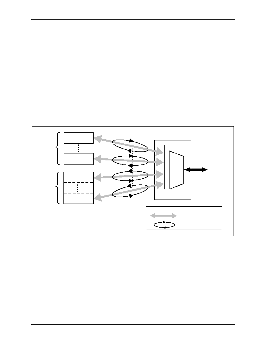
3.0 Host Interface
RS8234
3.2 Multiple Client Architecture
ATM ServiceSAR Plus with xBR Traffic Management
3-2
Mindspeed Technologies
TM
28234-DSH-001-B
3.2 Multiple Client Architecture
The RS8234 provides multiple independent control and status communication
paths. Each communication path, or flow, consists of a control queue and a status
queue for both segmentation and reassembly. The host assigns each of these
independent flows to system clients, or peers. As throughput requirements
escalate, the host system can add processing power in the form of additional
peers. This degree of freedom creates a scalable host environment. The RS8234
provides an ATM server for up to 32 clients.
Figure 3-1
illustrates this
client/server relationship.
3.2.1 Logical Clients
As shown in
Figure 3-1
, the clients need not be physically distinct PCI peers. The
host can also assign control and status queues to system software tasks, or logical
clients. Since the queues offer individually distinct communication paths, each
logical client interfaces to the RS8234 independently. Due to its server
architecture, the RS8234 supplies the synchronization between asynchronous
tasks requiring ATM services.
Figure 3-1. Client/Server Model of the RS8234
PCI Cards
PCI
Motherboard
Logical
Client
Logical
Client
ATM
User-Network
Interface
ATM Server
PCI
Interface
(Up to 32
Clients)
RS8234 Subsystem
Host Data Path
Host Control/Status Flow
LEGEND:
Physical
Client
Physical
Client
100074_011

RS8234
3.0 Host Interface
ATM ServiceSAR Plus with xBR Traffic Management
3.2 Multiple Client Architecture
28234-DSH-001-B
Mindspeed Technologies
TM
3-3
3.2.2 Resource Allocation
With either physical PCI peers, logical peers, or some combination of the two
types, the RS8234 multiplexes each peer's transmitted packets onto the line and
routes incoming packets to the appropriate peer. The host system allocates shared
resources, such as host and SAR shared memory, VPI/VCI address space, and
CBR time slots, to peers and clients arbitrarily.
3.2.3 Resource Isolation
Since each peer is assigned to an independent control and status path, the RS8234
isolates the resources of each peer. Not only does this simplify resource
management, but queue error conditions caused by a single peer do not affect any
other peers.
APPLICATION EXAMPLE
A system designer implements a RS8234 terminal as an ATM uplink for a
Service Access Multiplexer (SAM). The SAM is comprised of the ATM card and
several Frame Relay adapter cards. The host assigns each Frame Relay adapter
card to a set of RS8234 control and status queues at initialization. During opera
tion, one of the Frame Relay adapter cards experiences a hardware failure. The
failure prevents the card's processor from servicing the RS8234's reassembly status
queue. Eventually, the RS8234 fills the queue and is unable to proceed -- this situa-
tion is referred to as queue overflow. The RS8234 shuts down reassembly on VCCs
that are assigned to the overflowed queue only. Since the other cards in the
system are assigned to other status queues, their VCCs remain unaffected by the
failure.
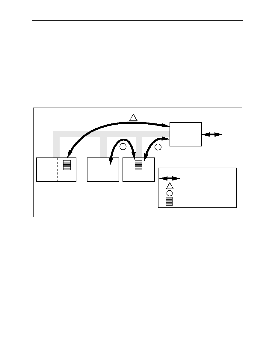
3.0 Host Interface
RS8234
3.2 Multiple Client Architecture
ATM ServiceSAR Plus with xBR Traffic Management
3-4
Mindspeed Technologies
TM
28234-DSH-001-B
3.2.4 Peer-to-Peer Transfers
The multiple queue architecture of the RS8234 also enables peer-to-peer PCI
transfers. The RS8234 transfers ATM cells as a PCI master. Since the buffer
control structures are independent for each peer, each identifies a unique address
range in PCI memory space. The host defines the address range of each peer. The
RS8234 transfers data within this address range. An address range corresponds
either to a region of centralized host memory, or to a set of peer resident buffers.
Figure 3-2
shows the difference between these two options. Centralized memory
buffers require store-forward operations, while the peer buffers enable
peer-to-peer transfers. Thus, peer-to-peer transfers reduce the use of the PCI bus.
Figure 3-2. Peer-to-Peer vs. Centralized Memory Data Transfers
PCI
Peer
Frame I/O
PCI
Host
Frame I/O
Peer
Memory
Centralized
Memory
PCI Motherboard
PCI Card
PCI BUS
RS8234
1
#
1
2
#
A
T
M
N
E
T
W
O
R
K
LEGEND:
PCI Transaction
Peer-to-Peer Transaction
Centralized Memory Transaction
Data Buffer
100074_012
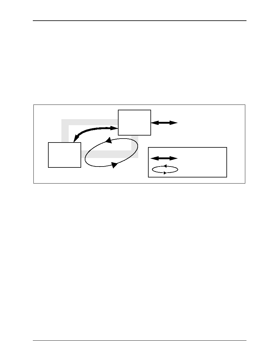
RS8234
3.0 Host Interface
ATM ServiceSAR Plus with xBR Traffic Management
3.2 Multiple Client Architecture
28234-DSH-001-B
Mindspeed Technologies
TM
3-5
3.2.5 Local Processor Clients
The RS8234 supports limited bandwidth SAR shared memory segmentation and
reassembly. Any peer may use the local processor port instead of the PCI bus for
control and status, as well as for data traffic. Hosts can use SAR shared memory
for control and status, but transfer data across the PCI bus. This "out-of-band"
control configuration diverts control overhead from the PCI bus, lessening the
burden of ATM's high throughput and robust management requirements on the
host system.
Figure 3-3
shows an out-of-band control architecture.
Figure 3-3. Out-of-Band Control Architecture
ATM
NETWORK
Host
System
RS8234
Subsystem
PCI BUS
Local Processor Port
LEGEND:
Data Flow
Host Control/Status Flow
100074_013

3.0 Host Interface
RS8234
3.3 Write-Only Control and Status
ATM ServiceSAR Plus with xBR Traffic Management
3-6
Mindspeed Technologies
TM
28234-DSH-001-B
3.3 Write-Only Control and Status
For host-based applications, the host manages the RS8234 SAR using write-only
control and status queues. This architecture minimizes PCI bus utilization by
eliminating reads from the control path. PCI writes utilize the bus much more
efficiently than PCI reads. During a PCI write, the target may "post" the write
data in an internal FIFO, terminate the transaction, and immediately release the
bus. On the other hand, during reads, the target retrieves the data while holding
the bus. Since the data retrieval takes some time, reads increase the PCI bus
utilization.
The RS8234's write-only architecture uses reads only for segmentation data
(PDU) fetches. All control and status transactions are writes. This section
describes the management of write-only queues. The purpose and entries of each
class of queue are described in later chapters.
Table 3-1
defines the RS8234 control and status queues.
3.3.1 Write-Only Control Queues
The host controls run-time segmentation and reassembly through write-only
control queues. There are two types of control queues -- the segmentation
transmit queues and the reassembly free buffer queues. The host submits buffers
of PDU data for segmentation on the transmit queues, and supplies empty buffers
for received data on the free buffer queues. Each type of queue is managed as a
write-only control queue.
These queues reside in SAR shared memory at a location defined by a base
register pointer. To allow multiple clients, the RS8234 supports 32 queues of each
type. The SAR and host manage each queue independently, through queue
management variables. The SAR stores its variables in internal registers called
base tables. The host maintains its own variables within its driver. Each queue
contains a programmable number of queue entries.
Table 3-1. RS8234 Control and Status Queues
Type
Segmentation
Reassembly
Control
Transmit queue
Free buffer queue
Status
Segmentation status queue
Reassembly status queue

RS8234
3.0 Host Interface
ATM ServiceSAR Plus with xBR Traffic Management
3.3 Write-Only Control and Status
28234-DSH-001-B
Mindspeed Technologies
TM
3-7
3.3.1.1 Control
Variables
Table 3-2
describes the variables for write-only control queues.
3.3.1.2 Queue
Management
Figure 3-4
illustrates the control queue management algorithm. The host
initializes all of the variables described in
Table 3-2
. Once the SAR is enabled, it
maintains the READ pointer. When the SAR processes a queue entry, it advances
the READ pointer (READ++). Since the queues are circular, the pointer will
eventually wrap back to zero. It also advances an internal counter, UPDATE
(UPDATE++). When INTERVAL queue entries have been processed, the SAR
writes its current position in the queue, READ, to a host variable, READ_UD.
The host determines the magnitude of INTERVAL at initialization. Larger
numbers result in fewer overhead PCI accesses, but will also introduce larger
latency between host updates, which reduces the effective size of the queue.
Table 3-2. Write-Only Control Queue Variables
Variable
Definition
Location
Initialization
WRITE
Current host position in queue
Host variable
0
READ_UD
Last known SAR position in queue as seen by
host
Host word aligned
variable
0
READ
Current SAR position in queue
SAR Base Table
0
INTERVAL
Number of queue entries processed by SAR
before writing READ_UD
SAR register
Host defined
UPDATE
Number of queue entries since last write of
READ_UD
SAR Base Table
0
READ_UD_PNTR
SAR pointer to READ_UD
SAR Base Table
&READ_UD
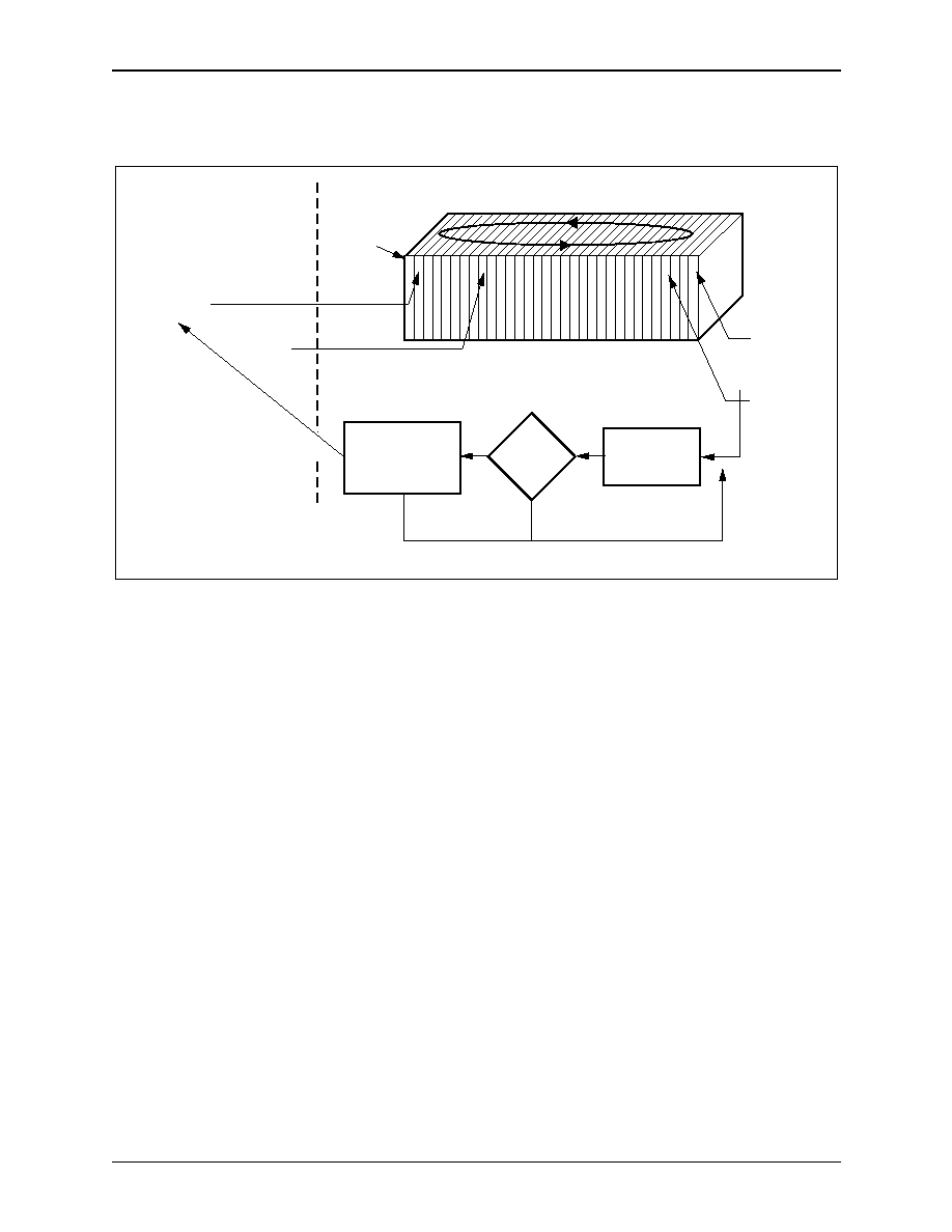
3.0 Host Interface
RS8234
3.3 Write-Only Control and Status
ATM ServiceSAR Plus with xBR Traffic Management
3-8
Mindspeed Technologies
TM
28234-DSH-001-B
The host also maintains a pointer into the queue, WRITE. When the host
submits a new entry, it must first ensure that the SAR has already processed the
entry location. The host compares WRITE to READ_UD. If (WRITE+1) modulo
size_of_queue equals READ_UD, then the host should halt writing to the queue.
This results in being able to use only N-1 queue entries. However, if this is not
done, then a full condition cannot be distinguished from an empty condition. The
host must wait until READ_UD is modified by the SAR before proceeding. This
algorithm ensures that the host does not overflow the control queue, without
reading the queue itself.
Once it has verified its ownership of the entry, the host writes the entry and
increments its write pointer (WRITE++). During this write, the host sets the valid
bit (VLD) in the entry to one.
The RS8234 "snoops" writes to the control queue areas. Once a write is
detected to a specific queue, the SAR attempts to process the queue entry at
READ. Before acting on the entry, the SAR checks for ownership of the entry,
indicated by the VLD bit. Once the RS8234 has processed the entry, it resets the
VLD bit to zero.
3.3.1.3 Underflow
Conditions
An underflow condition occurs when the SAR attempts to retrieve a queue entry
and the host has not yet supplied this entry. This condition only happens on the
free buffer queues. The SAR detects this condition by checking the queue entry
VLD bit. Once detected, the SAR enters an "Underflow Detected" state on this
queue only. Since this signifies that no data buffers are available for reassembly,
the SAR initiates EPD on all channels assigned to this queue.
Chapter 5.0
describes SAR handling of free buffer queue underflow in detail.
Figure 3-4. Write-Only Control Queue
0 0 0 0 0 0 0 0
1 1 1 1 1 1 1 1
1
1
1 1 1 1 1 1 1 1 1
1
0 0 0 0
READ_UD
WRITE++
READ_UD_PNTR (Base
Ta
ble)
PCI Bus
Boundary
VLD
bit
UPDATE=
INTERVAL
N
Y
UPDATE++
(Base Table)
READ++
Base
Register
Update Host
UPDATE=0
READ_UD_PNTR=
READ
100074_014

RS8234
3.0 Host Interface
ATM ServiceSAR Plus with xBR Traffic Management
3.3 Write-Only Control and Status
28234-DSH-001-B
Mindspeed Technologies
TM
3-9
3.3.2 Write-only Status Queues
The SAR reports status to the host through write-only status queues. Both the
segmentation and reassembly coprocessors use their own format of status queue.
However, the RS8234 manages all status queues with the same algorithm.
These queues reside in host memory, or optionally SAR shared memory, at a
location defined within the base table for each queue. The host must assign word
aligned (4-byte) status queue base addresses. To support multiple clients, the
RS8234 provides 32 queues of each type. The SAR and host manage each queue
independently through queue management variables. The SAR stores its variables
in internal base table registers. The host maintains its variables in its driver. Each
queue contains a programmable number of queue entries.
3.3.2.1 Control
Variables
Table 3-3
describes the variables for write-only status queue management.
Table 3-3. Write-only Status Queue Variables
Variable
Definition
Location
Initialization
WRITE
Current SAR position in queue
SAR Base Table
0
READ_UD
Last known host position in queue as seen by
SAR
SAR Base Table
0
READ
Current host position in queue
Host Variable
0
INTERVAL
Number of queue entries processed by host
before writing READ_UD
Host Variable
Host defined
UPDATE
Number of queue entries since last write of
READ_UD
Host Variable
0
READ_UD_PNTR
Host pointer to READ_UD
Host Variable
&READ_UD
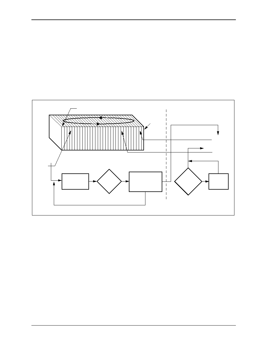
3.0 Host Interface
RS8234
3.3 Write-Only Control and Status
ATM ServiceSAR Plus with xBR Traffic Management
3-10
Mindspeed Technologies
TM
28234-DSH-001-B
3.3.2.2 Queue
Management
Figure 3-5
illustrates the status queue management algorithm. The host initializes
all of the variables described in
Table 3-3
.
The SAR maintains its own write pointer, WRITE. The RS8234 reports status
to the host by writing a status queue entry. After it writes the entry, the RS8234
increments its write pointer (WRITE++). This write also triggers a maskable
interrupt.
The host either responds to this interrupt, or periodically polls the status
queue. The VLD bit in each queue entry enables polling. The SAR sets the VLD
bit equal to one when it writes a status queue entry. The host resets it to zero after
processing an entry.
The host also maintains a pointer (READ) into the status queue. Each time it
services an entry, it increments a counter (UPDATE++). When this counter
reaches a host-specified threshold (INTERVAL), the host informs the SAR of its
current queue position by writing READ_UD in the queue's base table register.
Figure 3-5. Write-Only Status Queue
0 0 0 0 0 0 0 0
1 1 1 1 1 1 1 1
1
1
1 1 1 1 1 1 1 1 1
1
0 0 0 0
READ_UD
(Base Table)
WRITE++
(Base Table)
PCI Bus
Boundary
VLD
bit
UPDATE=
INTERVAL
N
N
Y
Y
UPDATE++
Signal
Overflow
READ++
BASE_PNTR
(Base table)
Update SAR
UPDATE=0
READ_UD_PNTR=
READ
WRITE =
READ_UD - 1
READ_UD_PNTR
100074_015

RS8234
3.0 Host Interface
ATM ServiceSAR Plus with xBR Traffic Management
3.3 Write-Only Control and Status
28234-DSH-001-B
Mindspeed Technologies
TM
3-11
3.3.2.3 Overflow
Conditions
An overflow condition occurs when the SAR attempts to write a status queue
entry, but the status queue entry is unavailable. This condition may happen for
both the segmentation and reassembly status queues. Chapter 4.0, Segmentation
Coprocessor, and Chapter 5.0, Reassembly Coprocessor, describe the handling of
this event. In either case, the result is severe and therefore undesirable. The host
control service rate of the status queue should match or exceed the status queue
reporting rate of the RS8234.
The RS8234 detects an overflow condition by comparing its current WRITE
pointer to the READ_UD pointer, i.e., the last known host READ position. If
WRITE points to the entry immediately before the READ_UD (WRITE =
READ_UD -1), the SAR detects the imminent overflow condition.
To inform the host of the event, the SAR sets the overflow indication bit
(OVFL) in the exhausted status queue. Since it cannot report status, the RS8234
segmentation and reassembly processing is temporarily halted for VCCs assigned
to the overflowed status queue only. All other processes and queues remain
operational.
3.3.2.4 Status Queue
Interrupt Delay
Status Queue Interrupt Delay has been added in order to reduce the interrupt
processing load on the host. This is valuable in a Network Interface Card
(NIC)-based solution, where the SAR resides in an environment in which the host
is not dedicated to datacom processing. Both a timer holdoff mechanism and an
event counter mechanism are implemented and work in parallel. The timer
holdoff mechanism uses the ALARM1 and CLOCK register resources to
implement an interval timer. Interrupts due to status queue writes, either host or
local, are delayed until the timer expires. The event counter mechanism delays the
assertion of the interrupt due to status queue writes until a fixed number of status
queue writes have occurred. Both mechanisms work in parallel (not in series) if
enabled, so that either mechanism needs to expire before the interrupt propagates
to the output pin. Interrupts due to conditions other than status queue writes are
not delayed. (See page 13-7 for specific information on the Interrupt Delay
(INT_DELAY) register.)
Timer Holdoff Mechanism
The timer holdoff mechanism is enabled by setting INT_DELAY (EN_TIMER)
to a logic high. The ALARM1 register is set to a value that will hold off the
interrupt for a specified period of time. The user initializes the CLOCK register
to zero. When the value in the CLOCK register is greater than the value in the
ALARM1 register, status queue interrupts will be allowed to propagate to the
appropriate interrupt pins, HINT* or PINT*. The CLOCK register is set to zero
once an interrupt has propagated to the output pin, thus closing the status queue
write interrupt window. The timer mechanism cannot be used in both the PINT*
and HINT* circuits at the same time. The timer mechanism is configured via the
INT_DELAY (TIMER_LOC) bit.

3.0 Host Interface
RS8234
3.3 Write-Only Control and Status
ATM ServiceSAR Plus with xBR Traffic Management
3-12
Mindspeed Technologies
TM
28234-DSH-001-B
Event Counter Mechanism
The event counter mechanism is enabled by setting INT_DELAY
(EN_STAT_CNT) to a logic high. An internal counter is implemented that counts
the number of status queue write events. The number of events before opening the
interrupt window is programmable via the INT_DELAY(STAT_CNT) field. The
window will be closed for STAT_CNT number of events. When the internal
counter has reached the value of STAT_CNT, the interrupt window will be
opened, which will allow the interrupt to propagate to the output pin. The counter
is reset when the status registers are read and the interrupt output goes inactive.

28234-DSH-001-B
Mindspeed Technologies
TM
4-1
4
4.0 Segmentation Coprocessor
4.1 Overview
ATM's cell transport mechanism enables large numbers of virtual channels or
VCCs to be multiplexed onto a single physical interface. The segmentation
process converts user data (typically Ethernet, Token Ring, or Frame Relay
packets) into ATM cells.
The RS8234 can segment 64 K VCCs simultaneously. The segmentation
coprocessor block independently segments each channel and multiplexes the
VCCs onto the line with cell level interleaving. The RS8234 xBR Traffic
Manager determines the order of execution of these independent processes to
ensure the requested QoS for every channel. For each cell transmission
opportunity, the xBR Traffic Manager tells the segmentation coprocessor which
VCC to send. Therefore, the segmentation coprocessor acts as a slave to the xBR
Traffic Manager.
In addition to converting blocked user data into ATM cells, the RS8234
generates all AAL overhead for AAL3/4 and AAL5, or optionally uses a null
adaptation layer, AAL0. The RS8234 also generates the ATM cell header, as
defined by the host, for each VCC. Furthermore, the segmentation coprocessor
and xBR Traffic Manager together provide service specific features to enhance
the performance of Frame Relay internetworking and LAN Emulation.

4.0 Segmentation Coprocessor
RS8234
4.2 Segmentation Functional Description
ATM ServiceSAR Plus with xBR Traffic Management
4-2
Mindspeed Technologies
TM
28234-DSH-001-B
4.2 Segmentation Functional Description
4.2.1 Segmentation VCCs
A VCC specifies a single VC or VP in the ATM network. The RS8234 supports
up to 64 K segmentation VCCs, referenced by a unique index, VCC_INDEX. The
VCC_INDEX identifies a location in the Segmentation VCC Table, an array of
10-word segmentation VCC channel descriptors.
Except for ABR service category VCCs, each segmentation VCC occupies a
single descriptor in the table (10 words). Due to the large number of specified
parameters for ABR traffic, ABR VCCs occupy two descriptors (20 words) in the
Segmentation VCC Table. The VCC_INDEX for ABR VCCs points to the first of
the two descriptors, and must be evenly divisible by two.
A Segmentation VCC Table channel descriptor consists of two parts: an AAL
specific VCC Table Entry (seven words) and a service class specific Schedule
State (SCH_STATE). For non-ABR VCCs, the remaining three words of the
channel descriptor form the SCH_STATE entry. For an ABR VCC, the
SCH_STATE entry contains 13 words, which require an additional descriptor
location.
4.2.1.1 Segmentation
VCC Table
Figure 4-1
shows a VCC Table with a CBR VCC at VCC_INDEX 3, an ABR
VCC located at VCC_INDEX 0x1000, and a non-ABR VCC at VCC_INDEX
0xFFFD. The host allocates the VCC Table in SAR shared memory and provides
an address to the SAR in a base register field, SEG_VBASE(SEG_VCCB). For
the most efficient ABR performance, all ABR VCCs should be placed in the
upper half of the VCC Table (i.e., with smaller VCC indexes). The only reason
not to put ABR VCCs at the lowest address range is to place CBR VCCs in the
first 32k of VCC addresses. Valid VCC indexes for CBR traffic range from
0x0000 to 0x7FFE, due to the limit imposed by a 15-bit address. A VCC index of
0xFFFF for non-CBR and 0x7FFF for CBR indicates a NULL VCC.
While the RS8234 will accept any VCC Index within the range of 64 K VCC
Indexes, the actual number of segmentation VCCs allowed by the SAR is limited
by the amount of SAR shared memory available in which to allocate and create
segmentation VCC Tables, transmit queues, etc.
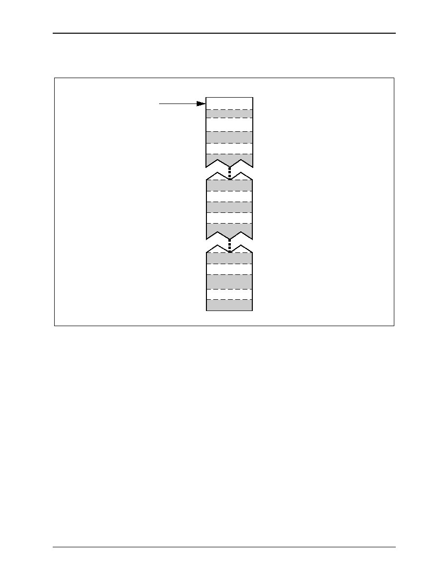
RS8234
4.0 Segmentation Coprocessor
ATM ServiceSAR Plus with xBR Traffic Management
4.2 Segmentation Functional Description
28234-DSH-001-B
Mindspeed Technologies
TM
4-3
The VCC Table entry contains generic information common to all traffic
classes. This includes a default ATM header, which the host may modify during
the segmentation process. See
Section 4.3.1
for full details of the structure of a
segmentation VCC Table entry.
4.2.1.2 VCC
Identification
The host allocates a region of SAR shared memory for the segmentation VCC
Table at system initialization, based on the maximum number of connections and
the maximum number of ABR connections. The host informs the SAR of the
location of the table through the internal base register, SEG_VBASE
(SEG_VCCB).
Once a table has been established, the host assigns segmentation VCCs to
entries in the table. The host describes the SEG VCC by initializing the SEG VCC
Table entry including the SCH_STATE portions of the assigned VCC. The
VCC_INDEX, defined as the offset into the table in 10-word increments,
uniquely identifies a segmentation channel. In all communication between the
SAR and the host, a VCC_INDEX field specifies a VCC.
Figure 4-1. Segmentation VCC Table
SCH_STATE
SCH_STATE
Base Register
(SEG_VBASE(SEG_VCCB)<<5)
VCC_INDEX = 0x3
(CBR VCC)
VCC_INDEX = 0x1000
(ABR VCC)
VCC_INDEX = 0xFFFD
(non-ABR VCC)
VCC_INDEX = 0x0
VCC Table
10 Words = 1 Descriptor
7 Words
3 Words
1 Descriptor
7 Words
13 Words
2 Descriptors
VCC Table Entry
SCH_STATE
}
}
}
}
}
}
}
VCC Table Entry
VCC Table Entry
100074_016

4.0 Segmentation Coprocessor
RS8234
4.2 Segmentation Functional Description
ATM ServiceSAR Plus with xBR Traffic Management
4-4
Mindspeed Technologies
TM
28234-DSH-001-B
4.2.2 Submitting Segmentation Data
Once the host establishes a connection, it supplies data for segmentation. The host
submits full or partial PDUs, either one at a time or in batches, for individual
VCCs. The SAR accepts PDUs at any time, regardless of the state of the
connection, and segments data on each VCC independently.
4.2.2.1 User Data
Format
The RS8234 accepts user PDUs as sequences of data buffers. SAR shared
memory resident segmentation buffer descriptors (SBDs) provide the address,
length and control information for buffers. The host forms PDU buffer sequences
by linking buffer descriptors. The data buffers themselves contain only user data
and reside in host (or optionally SAR shared) memory. Host data buffers contain
the bulk of segmentation data, and can begin on any byte-aligned address in the
SAR's PCI address space.
NOTE:
SAR shared memory data buffer segmentation should be limited to low
bandwidth applications, such as Signalling, OAM, and ILMI.
4.2.2.2 Buffer
Descriptors
The host submits data using the following process sequence. First, the host
allocates an SBD for each buffer in a message. SBDs reside in SAR shared
memory, and must begin on word-aligned addresses. Then, the host describes the
buffers in the SBD. This description includes the address and length of the buffer,
as well as control fields for the SAR during buffer segmentation. These control
fields specify the VCC_INDEX, the AAL type, and header override information
for the buffer.
The host then creates PDU message sequences by concatenating buffers. The
host forms the buffer sequence by linking a list of buffer descriptors using the
SBD's NEXT field. Two bits in the SBD control fields delineate the beginning
and end of messages. One bit, BOM, specifies that the buffer contains the
beginning of a message. The second bit, EOM, notifies the SAR that the buffer
contains the end of the current message. The host identifies the end of the SBD
chain by terminating the list with a NULL (0) NEXT pointer.
Table 4-1
shows the
appropriate use of these bits in detail.
Table 4-1. Segmentation PDU Delineation
BOM
EOM
Buffer to Message Adaptation
0
0
Segment as Continuation of Message (COM).
0
1
Terminate current CPCS-PDU at end of buffer (EOM).
1
0
Restart CPCS-PDU generation (BOM). Wait for EOM for termination.
1
1
Buffer contains complete message. Restart/terminate CPCS-PDU.
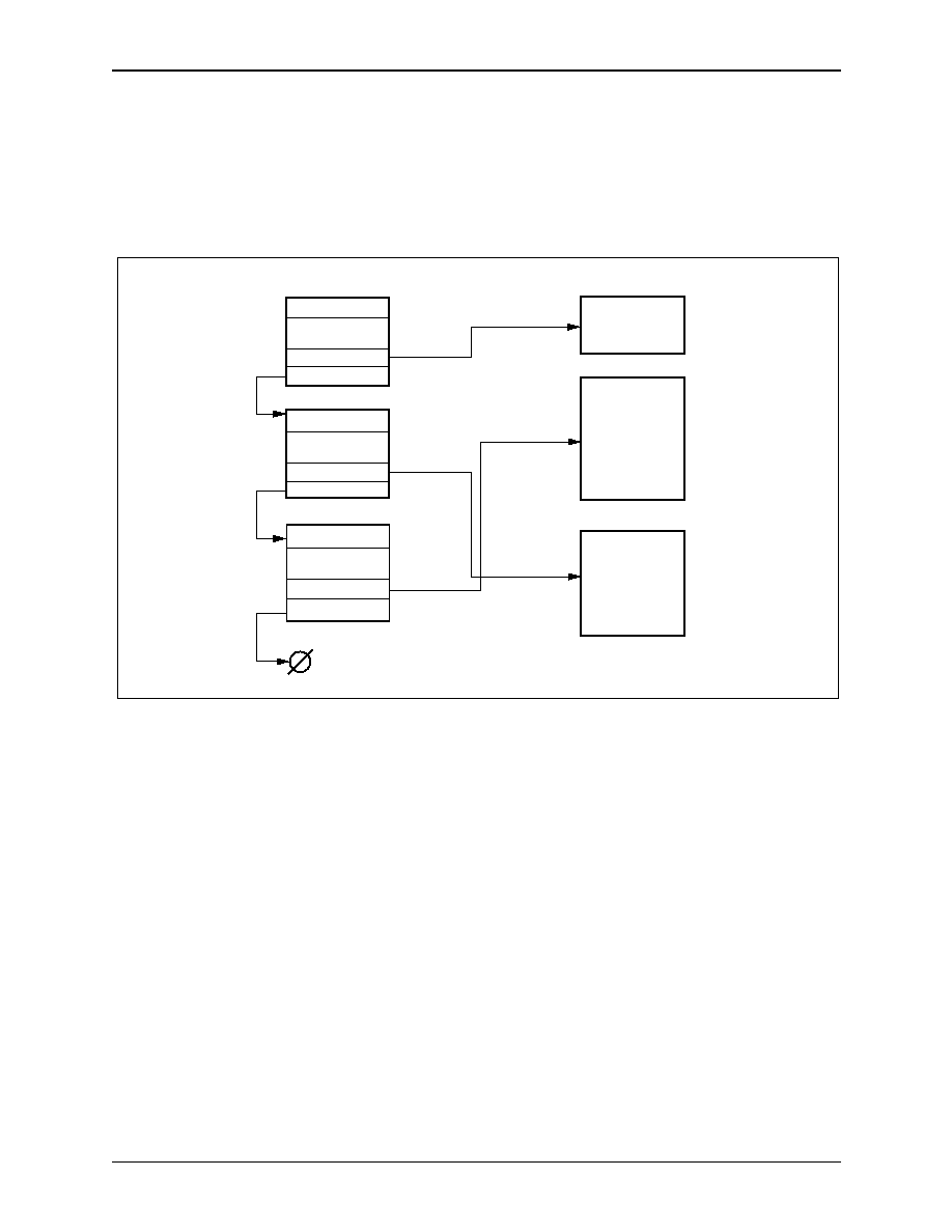
RS8234
4.0 Segmentation Coprocessor
ATM ServiceSAR Plus with xBR Traffic Management
4.2 Segmentation Functional Description
28234-DSH-001-B
Mindspeed Technologies
TM
4-5
4.2.2.3 Host Linked
Segmentation Buffer
Descriptors
Figure 4-2
shows an example of SBD chaining. The host has formed a
three-buffer message by linking three SBDs. In this example, the SAR will
transmit a message sequence of buffer A, then buffer B, and finally buffer C as
the end of message.
4.2.2.4 Transmit Queues
Once the linked list of SBDs is complete, the host submits the chained message to
the SAR for segmentation. The host uses one of the 32 transmit queues for this
purpose. Each transmit queue is a circular queue of one-word entries. The host
identifies the next available transmit queue entry according to the write-only host
interface specification described in
Section 3.3.1
. The host processor writes a
pointer to the SAR shared memory SBD onto the next available transmit queue
entry. During this write, the host also sets the VLD bit to indicate the entry is
valid.
The RS8234 detects this write by "snooping" SAR shared memory accesses.
When a write occurs to any of the transmit queues, the RS8234 marks that queue
as pending. Once every cell slot, the RS8234 services one queue entry from one
Transmit Queue. The system designer selects one of two service order priority
schemes. With the SEG_CTRL(TX_RND) bit set to one, the RS8234 services
queues in round-robin order (i.e., one entry per queue in transmit queue sequence
for all active queues). With the SEG_CTRL(TX_RND) bit set to zero, the
RS8234 services the queues in fixed priority order (i.e., entries from higher
priority active queues are serviced before lower priority queue entries, with
transmit queue 31 having highest priority).
Figure 4-2. Segmentation Buffer Descriptor Chaining
SAR Shared Memory
Host (or SAR Shared) Memory
VCC_INDEX = 4
VCC_INDEX = 4
CONTROL
<BOM>
CONTROL
<COM>
BUFF_PNTR
BUFF_PNTR
NEXT
NEXT
VCC_INDEX = 4
CONTROL
<EOM>
BUFF_PNTR
NEXT
(NULL)
A
C
B
Buffers
SBDs
100074_017
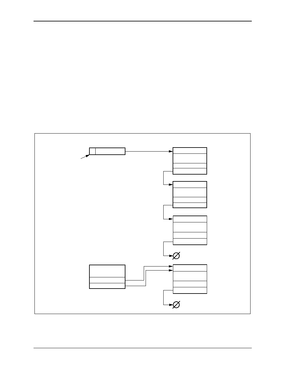
4.0 Segmentation Coprocessor
RS8234
4.2 Segmentation Functional Description
ATM ServiceSAR Plus with xBR Traffic Management
4-6
Mindspeed Technologies
TM
28234-DSH-001-B
In either case, the SAR services one transmit queue entry by linking the new
buffer descriptor chain to the VCC Table entry identified by the VCC_INDEX in
the first SBD. The VCC Table entry includes pointers to buffer descriptors for
segmentation. The SAR will link the new SBDs to the current chain of SBDs on a
VCC. The host can submit data to a VCC while the SAR is segmenting a
previously submitted message. Once the chain has been linked, the RS8234 resets
the transmit queue VLD bit to zero.
SAR Transmit Queue
Processing
Figure 4-3
and
Figure 4-4
illustrate the process of linking SBDs to a VCC Table
entry.
NOTE:
Note that as the new buffers are submitted, the VCC is processing a single
buffer PDU (BOM/EOM). The RS8234 accepts new PDUs while it is
processing outstanding buffers.
Figure 4-3. Before SAR Transmit Queue Entry Processing
Transmit Queue Entry
VCC_INDEX = 4
BD_PNTR
VCC STATE
CURR_DESCR
LAST_DESCR
VCC_INDEX = 4
CONTROL
<BOM>
CONTROL
<COM>
BUFF_PNTR = &A
BUFF_PNTR = &B
NEXT
NEXT
VCC_INDEX = 4
CONTROL
<EOM>
BUFF_PNTR = &C
NEXT
VCC_INDEX = 4
CONTROL
<BOM/EOM>
BUFF_PNTR = &Z
NEXT
(NULL)
(NULL)
SBDs
1
HOST WRITE
(VLD = 1)
SEG VCC Table Entry (VCC_INDEX = 4)
100074_018

RS8234
4.0 Segmentation Coprocessor
ATM ServiceSAR Plus with xBR Traffic Management
4.2 Segmentation Functional Description
28234-DSH-001-B
Mindspeed Technologies
TM
4-7
4.2.2.5 Partial PDUs
The host may submit partial PDUs to the RS8234. In this case, the SAR transmits
the data and halts on a cell boundary. The partial PDU buffers are not required to
be aligned to a cell boundary by the host. The RS8234 tracks the remaining
segmentation data. If a partial cell remains, the RS8234 will hold the buffer until
it can complete a cell. Once the host submits an additional buffer, the RS8234
resumes segmentation.
4.2.2.6 Virtual Paths
For network management simplicity, the host can create Virtual Path VCCs
(i.e., it can segment many VCIs on one VP). The host supplies the VCI for the
ATM header within each Segmentation Buffer Descriptor (SBD). When using this
method, the RS8234 must be provided with contiguous linked SBDs that are of
the same VCC_INDEX (i.e., the same VCI) for the length of the PDU. This
allows the RS8234 to multiplex VCI messages at the PDU level. For AAL5
segmentation, the host must guarantee that SBDs are linked with PDU
multiplexing to preserve CPCS-PDU integrity.
Figure 4-4. After SAR Transmit Queue Entry Processing
Transmit Queue Entry
VCC_INDEX = 4
BD_PNTR
VCC STATE
CURR_DESCR
LAST_DESCR
VCC_INDEX = 4
CONTROL
<BOM>
CONTROL
<COM>
BUFF_PNTR = &A
BUFF_PNTR = &B
NEXT
NEXT
VCC_INDEX = 4
CONTROL
<EOM>
BUFF_PNTR = &C
NEXT
VCC_INDEX = 4
CONTROL
<BOM/EOM>
BUFF_PNTR = &Z
NEXT
(NULL)
0
SAR WRITE
(VLD = 0)
SEG VCC Table Entry (VCC_INDEX = 4)
100074_019
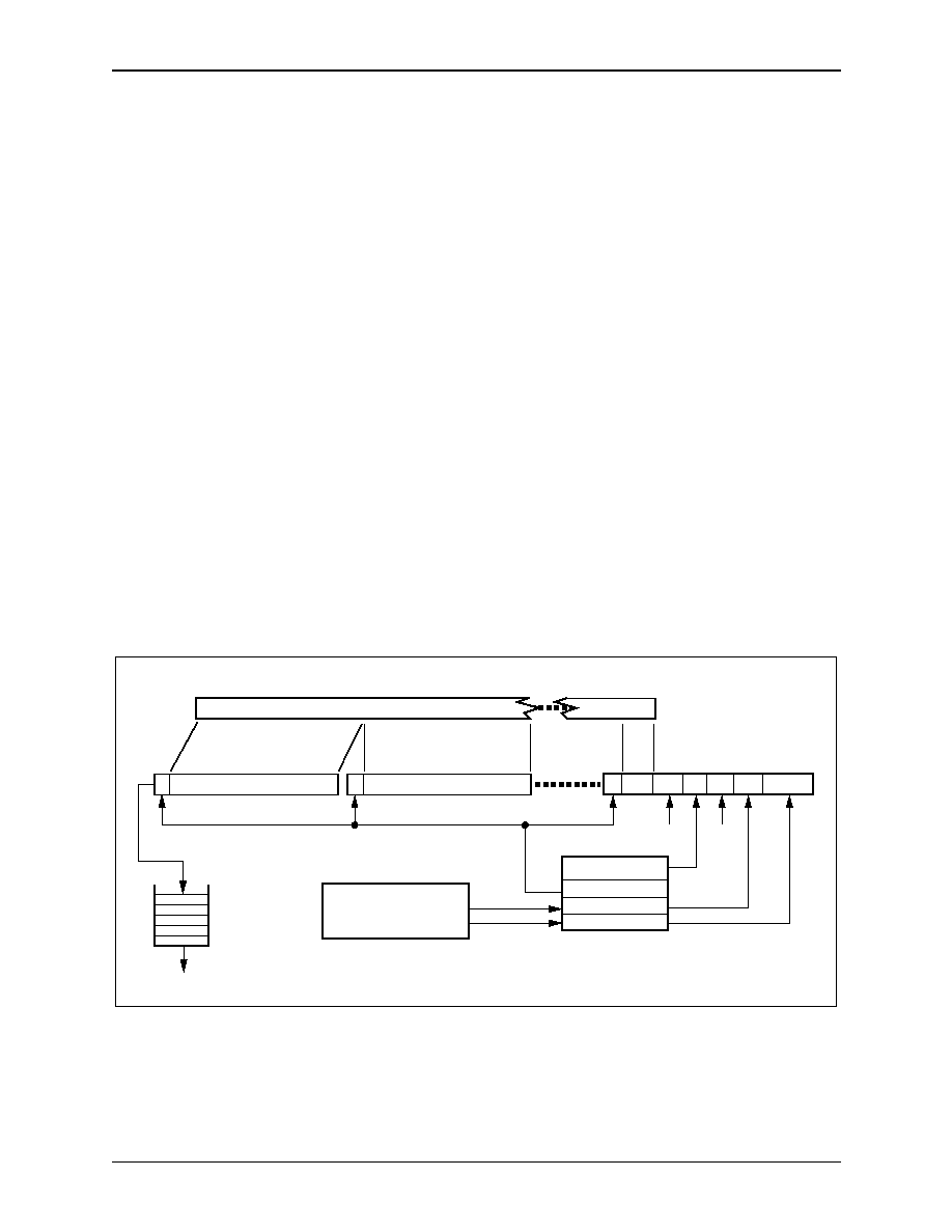
4.0 Segmentation Coprocessor
RS8234
4.2 Segmentation Functional Description
ATM ServiceSAR Plus with xBR Traffic Management
4-8
Mindspeed Technologies
TM
28234-DSH-001-B
4.2.3 CPCS-PDU Processing
The buffers submitted by the user contain only user data, the CPCS Service Data
Unit (CPCS-SDU). The RS8234 adds the CPCS-PDU protocol fields to the
CPCS-SDU. The SAR supports three AAL levels: AAL5, AAL3/4, and a
transparent adaptation layer (AAL0).
Specific features also allow the generation of OAM cells.
Chapter 7.0
covers
OAM generation in detail.
4.2.3.1 AAL5
For AAL5, the SAR generates the CPCS-PDU trailer, and pads the CPCS-SDU to
align the PDU to a cell boundary. The RS8234 generates the PAD, Length (LEN),
Common Part Indicator (CPI), and Cyclic Redundancy Check (CRC) fields
according to I.363. The host supplies the CPCS User-to-User Indication (UU)
field in the first buffer descriptor in a message, and the RS8234 transmits it
following I.363.
The SAR generates the ATM header according to host-initialized settings in
the VCC Table Entry. The RS8234 terminates AAL5 PDUs by setting bit zero of
the Payload Type Identifier field, PTI[0] = 1.
The host aborts PDUs by activating an EOM SBD abort option. The host
activates this by setting the following fields in the SEG buffer descriptor entry to
these values: AAL_MODE = AAL5 (b00), and AAL_OPT = ABORT (b01).
Figure 4-5
shows the RS8234's AAL5 PDU generation scheme. The SAR uses
internal circuits to generate and store PDU length and CRC-32 in the SEG VCC
Table. The RS8234 transmits these fields within the EOM cell. The PAD and CPI
fields are generated internally.
Figure 4-5. AAL5 CPCS-PDU Generation
USER DATA BUFFER(S)
H
H
H
PAD UU CPI LEN CRC-32
UU
ATM_HEADER
PDU_LEN
CRC_REM
SEG VCC Table Entry
Internal
Byte Length Counter
CRC Accumulator
Circuits
(Set PTI[0] = 1)
TX_FIFO
(1-9 Cells)
PHY Interface
100074_020

RS8234
4.0 Segmentation Coprocessor
ATM ServiceSAR Plus with xBR Traffic Management
4.2 Segmentation Functional Description
28234-DSH-001-B
Mindspeed Technologies
TM
4-9
4.2.3.2 AAL3/4
When a segmentation buffer descriptor's AAL_MODE field is set to AAL3/4
(value = b10), the RS8234 generates the CPCS-PDU's CPI, Btag, Etag, BASize,
Alignment (AL), and Length fields in the header and trailer of the CPCS-PDU,
and pads the PDU to align to a cell boundary.
On the first cell of a buffer with BOM set, the segmentation coprocessor
generates the CPCS-PDU header fields as the first four bytes of the first
SAR-PDU's payload.
On the last cell of a buffer with EOM set, the segmentation coprocessor writes
an all-zeros PAD field after the end of the segmentation buffer data to
complement the CPCS-PDU payload to an integral number of four-byte words.
The segmentation coprocessor then adds the four-byte CPCS-PDU trailer and
then fills octets with zeros for the remainder of the SAR-PDU payload.
Each CPCS-PDU field is generated as shown in
Table 4-2
.
The RS8234 also generates the SAR-PDU's Segment Type (ST), Sequence
Number (SN), Message Identification (MID), Length Indication (LI) and CRC
fields in each segmented cell for that CPCS-PDU.
Each AAL3/4 cell carries 44 octets of payload and four octets (five fields) of
header and trailer information. On the last generated cell for a CPCS-PDU with
the EOM set in the buffer descriptor, the segmentation coprocessor will pad the
SAR-PDU payload with 0 to 44 bytes.
Table 4-2. AAL3/4 CPCS-PDU Field Generation
Field
# Bits
Function
CPI
8
Common Part Identifier; set to zero.
BTAG
8
Beginning Tag; read from SEG VCC Table entry.
BASIZE
16
Buffer Allocation Size; read from SEG Buffer Descriptor entry.
AL
8
Alignment Filler, aligns the trailer to fit a 32-bit word.
ETAG
8
Ending Tag; read from SEG VCC Table entry.
LENGTH
16
CPCS-PDU Length; the calculated size of the PDU's payload.

4.0 Segmentation Coprocessor
RS8234
4.2 Segmentation Functional Description
ATM ServiceSAR Plus with xBR Traffic Management
4-10
Mindspeed Technologies
TM
28234-DSH-001-B
Each SAR-PDU field is generated as shown in
Table 4-3
.
Table 4-4
shows the settings for the ST (Segment Type) field.
Table 4-3. AAL3/4 SAR-PDU Field Generation
Field
# Bits
Function
ST
2
�
BOM value for the first cell generated from the buffer with
the BOM option in the buffer descriptor set.
�
EOM value for the last cell generated from the buffer with
the EOM option in the buffer descriptor set.
�
SSM value for the cell generated from the buffer with both
BOM and EOM options in the buffer descriptor set, and
the buffer descriptor LENGTH field
44.
�
COM value for all other generated cells.
(See the next table for Binary values.)
SN
4
Read from the SN field in the SEG VCC structure. The SN field
is incremented modulo 16 after each use.
MID
10
Read from the MID field in the SEG VCC structure.
LI
6
Generated by the segmentation coprocessor in an internal
byte length counter.
CRC
10
Generated as all zeros. The CRC field may be overwritten with
the CRC-10 generator before transmission by setting the
CRC_10 option in the seg buffer descriptor.
Table 4-4. Coding of Segment Type (ST) Field
Segment Type
Encoding
Usage
BOM
10
Beginning of Message
COM
00
Continuation of Message
EOM
01
End of Message
SSM
11
Single Segment Message
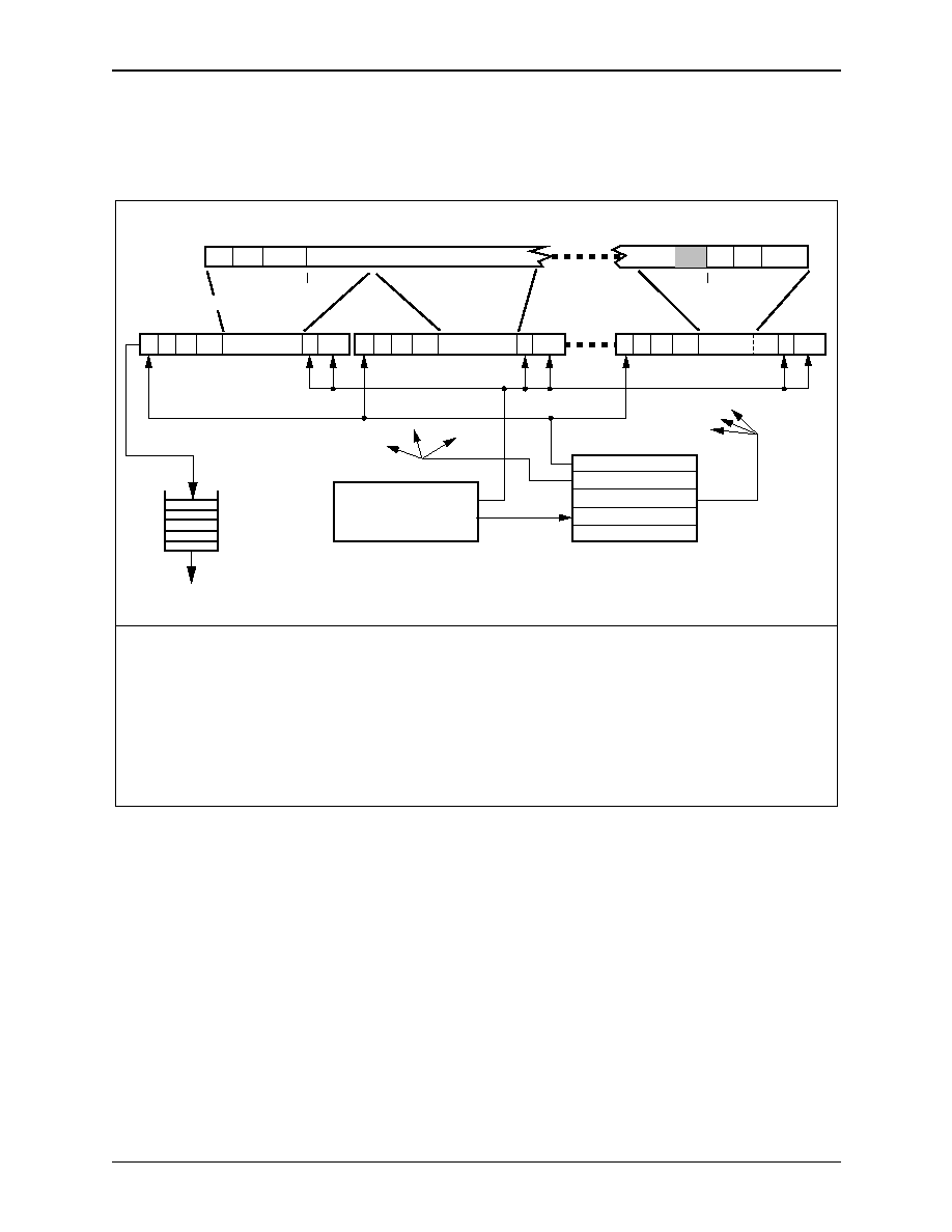
RS8234
4.0 Segmentation Coprocessor
ATM ServiceSAR Plus with xBR Traffic Management
4.2 Segmentation Functional Description
28234-DSH-001-B
Mindspeed Technologies
TM
4-11
Figure 4-6
shows the RS8234's AAL3/4 PDU generation scheme.
4.2.3.3 AAL0
The RS8234 also supports a transparent or NULL adaptation layer, AAL0. AAL0
maps CPCS-SDUs directly to CPCS-PDU payloads. The SAR pads the SDU to a
48-byte cell payload boundary, but generates no other overhead. The SAR
generates the ATM header and PDU termination indications in the same manner
as it does with AAL5.
4.2.4 ATM Physical Layer Interface
Once the segmentation coprocessor has formed an ATM cell, the RS8234
transfers the cell to the transmit FIFO. The user chooses the length of this FIFO,
with possible sizes from one to nine cells. The FIFO depth is programmable,
since there is a trade-off between absorbing PCI latency with a longer FIFO, and
introducing greater jitter.
Section 6.2.3.3
discusses this trade-off in greater depth.
Once sent to the transmit FIFO, the cell passes through the FIFO to the PHY layer
interface circuits.
Figure 4-6. AAL3/4 CPCS-PDU Generation
H ST SN MID
Information
LI CRC
Length
Etag
AL
PAD
Trailer
CPI Btag BASIZE
<64 K
Header
(44 bytes)
Payload
Convergence Sublayer (CPCS-PDU)
H ST SN MID
LI CRC
H ST SN MID
LI CRC
Pad
Segmentation (SAR-PDU)
(To Each
Seqmentented
Cell)
(To Each
Seqmented
Cell)
SEG VCC Table Entry
TX_FIFO
(1-9 Cells)
PHY
INTERFACE
Internal
Byte Length Counter
CRC Accumulator
Circuits
ATM_ HEADER
SN
MID
PDU_LEN
BETAG
100074_021
NOTE(S):
1. CPI = Common Part Indicator. In AAL3/4, initially set to all Os.
2. Btag = Beginning Tag. Has the same identifying number as the Etag field. When the receiver reassembles a long PDU,
these tags help identify that cells are from the same PDU.
3. BASIZE = Buffer Allocation Size. Tells the receiver how large the buffer allocation must be to receive and reassemble
this PDU.
4. AL = Aligns the trailer to fit a 4-byte word.
5. Etag = Ending Tag (see Btag above).
6. Length = Contains the exact size of the PDU's payload.

4.0 Segmentation Coprocessor
RS8234
4.2 Segmentation Functional Description
ATM ServiceSAR Plus with xBR Traffic Management
4-12
Mindspeed Technologies
TM
28234-DSH-001-B
4.2.5 Status Reporting
The RS8234 informs the host of segmentation completion using segmentation
status queues. The host assigns each VCC to one of 32 status queues, enabling a
multiple peer architecture as described in
Section 3.2
. The RS8234 reports status
entry on either PDU or buffer boundaries, selectable on a per-VCC basis by
setting the STM_MODE bit. PDU boundary status is referred to as Message
Mode, while buffer status reporting is called Streaming Mode. Error conditions
also generate status queue entries, though this is a rare occurrence within a
RS8234 subsystem's segmentation block. The segmentation status queues operate
according to the write-only host interface, defined in
Section 3.3.2
.
The RS8234 returns a user supplied field (USER_PNTR) from the first SBD
associated with the status entry. The SAR does not use this field for any internal
purpose; it simply circulates the information back to the host. The value of
USER_PNTR must uniquely describe the segmented buffer associated with the
SBD. USER_PNTR may contain the address of the buffer or of a host data
structure describing the buffer. To simplify host management, the RS8234 also
returns the VCC_INDEX of the VCC on which the buffer was transmitted.
4.2.6 Virtual FIFOs
In addition to gathering PDU data from buffers, the RS8234 provides an optional
method to segment from a fixed PCI address, or Virtual FIFO. The RS8234
supports AAL0, CBR Virtual FIFO segmentation.
The host configures the channel for Virtual FIFO operation by setting the
CURR_PNTR and RUN fields to zero in the SEG VCC Table entry. The host
writes the FIFO address to the FIFO_PNTR field in the VCC Table entry. The
host also initially sets the SCH_MODE field = CBR.
At this point, the host can start writing cells to the external host transmit FIFO.
Once the FIFO is almost full, the host sets the RUN bit to a logic high. The SAR
will then start reading from the FIFO. When the FIFO gets below almost empty,
the host will set the SCH_OPT bit to a logic high. The SAR will then skip a cell
transmit opportunity in order to allow the FIFO to refill. After the SAR skips a
cell, it will reset the SCH_OPT bit to a logic low.
In this mode, the segmentation coprocessor reads 48 bytes of payload from the
host FIFO, and prepends (i.e., attaches to the beginning) the ATM_HEADER
value in the VCC Table entry. The host does not use the transmit queue for Virtual
FIFOs. The RS8234 transmits cell payloads from this location indefinitely, with
no status reporting.

RS8234
4.0 Segmentation Coprocessor
ATM ServiceSAR Plus with xBR Traffic Management
4.3 Segmentation Control and Data Structures
28234-DSH-001-B
Mindspeed Technologies
TM
4-13
4.3 Segmentation Control and Data Structures
4.3.1 Segmentation VCC Table Entry
Each Segmentation VCC Table entry occupies one 10-word descriptor of the
Segmentation VCC Table. The first seven words are generic, independent of
traffic class. The last 3 or 13 words provide additional parameters specific to
service classes.
There are two basic formats for the generic part of the VCC Table Entry:
AAL3/4-AAL5-AAL0, and Virtual FIFO. Each completely describe the state of
the segmentation process for individual VCCs.
Table 4-7
and
Table 4-8
describe
the format of AAL3/4, AAL5, and AAL 0 VCC Table Entries.
4.0 Segmentation Coprocessor
RS8234
4.3 Segmentation Control and Data Structures
ATM ServiceSAR Plus with xBR Traffic Management
4-14
Mindspeed Technologies
TM
28234-DSH-001-B
KEY:
= Written by host at VCC setup
= May be dynamically modified during active segmentation
Table 4-5. Segmentation VCC Table Entry - AAL3/4-AAL5-AAL0 Format
Word 31 30 29 28 27 26 25 24 23 22 21 20 19 18 17 16 15 14 13 12 11 10 9
8
7
6
5
4
3
2
1
0
0
PM_INDEX
Rs
vd
ACK_
PM
FWD_PM
Rs
vd
LAST_PNTR
1
UU
Rsvd
BOM_PNTR
2
ATM_HEADER
3
PDU_LEN
BUFFER_LEN
4
(1)
CRC_REM
4
(2)
Reserved
BETAG
Rsvd
SN
MID
5
S
T
M_
MO
DE
STAT
PM
_
E
N
LAST
_C
LP
RUN
NX_
E
OM
Rs
vd
CURR_PNTR
6
SCH
BCK_PM
VPC
SCH_
GFR/CBR_
W_
T
U
N
FLO
W
_
S
T
GF
R_
PRI
SCH_
MOD
E
PRI
SCH_
OP
T
NEXT_VCC
7-9/19
SCH_STATE
NOTE(S):
(1)
This word is used for AAL5 and AAL0 VCCs.
(2)
This word is used for AAL3/4 VCCs.

RS8234
4.0 Segmentation Coprocessor
ATM ServiceSAR Plus with xBR Traffic Management
4.3 Segmentation Control and Data Structures
28234-DSH-001-B
Mindspeed Technologies
TM
4-15
Table 4-6. Segmentation VCC Table Entry - AAL3/4, 5, and 0 Field Descriptions (1 of 2)
Field Name
Description
PM_INDEX
Performance Monitoring index. 128 VCCs may be selected for automatic OAM PM generation.
Each monitored VCC has a unique performance monitoring index.
If this field is changed while the VCC is active, only the byte containing the field should be written.
(See
Chapter 6.0
).
ACK_PM
Toggled after each backward reporting PM cell is sent. Used to prevent PM information in PM
table from being overwritten before cell is sent.
FWD_PM
Indicates that next cell should be a forward monitoring PM cell.
LAST_PNTR
Points to last buffer descriptor currently linked to the VCC. The two least significant bits of the
pointer are assumed to be zero (word-aligned). The address of the buffer descriptor is
(LAST_PNTR << 2) or (LAST_PNTR * 4).
UU
AAL5 User-to-User indication. This field is copied from the buffer descriptor UU field. The RS8234
inserts the UU field in the CPCS-PDU trailer contained in the EOM cell.
BOM_PNTR
In Message mode (STM_MODE=0), points to the first buffer descriptor of a message composed
of more than one buffer descriptor. The RS8234 returns the corresponding USER_PNTR from this
buffer descriptor in the status queue.
In Streaming mode (STM_MODE=1) it is not used.
The two least significant bits of the pointer are assumed to be zero (word-aligned). The
address of the buffer descriptor is (BOM_PNTR << 2) or (BOM_PNTR * 4).
ATM_HEADER
Used for each ATM cell for the VCC. The transmitted header may be modified by option bits in the
current buffer descriptor.
PDU_LEN
CPCS-PDU Trailer Length field. This field is generated by the SAR and inserted in the Length field
of the EOM cell.
BUFFER_LEN
Buffer Length. The number of bytes of data read from the current segmentation buffer.
CRC_REM
Accumulated value of AAL5 32-bit CRC, calculated on-the-fly by the SRC and appended to the
PDU at EOM.
BETAG
AAL3/4 Btag and Etag fields.
SN
AAL3/4 Sequence Number field.
MID
AAL3/4 Message Id field.
STM_MODE
Streaming Status Mode.
0 = Message Mode: a status entry is written (with a corresponding maskable interrupt) only
when the last buffer in a message completes segmentation. The status entry written
corresponds to the first buffer descriptor in the message.
1 = Streaming Mode: a status entry is written (with a corresponding maskable interrupt) for
each buffer as it completes segmentation.
STAT
Identifies the Segmentation Status Queue used for all status entries.
PM_EN
Enables performance monitoring for the VCC. If this bit is changed while the VCC is active, only
the byte containing the bit should be written. (See
Chapter 6.0
.)
LAST_CLP
Last transmitted CLP bit for VCC. This bit is updated by the SRC after each transmitted cell. This
bit is in the same word as the PM_EN bit, and is copied by the SAR from the current buffer
descriptor. The bit is used to select the correct VBR bucket for certain VBR VCCs.

4.0 Segmentation Coprocessor
RS8234
4.3 Segmentation Control and Data Structures
ATM ServiceSAR Plus with xBR Traffic Management
4-16
Mindspeed Technologies
TM
28234-DSH-001-B
RUN
Flag that indicates that segmentation is proceeding. This flag is set to one by the SAR when the
host supplies data for the VCC; it is set to zero by the SAR when the data available for the VCC is
not sufficient to send at entire ATM cell.
NX_EOM
Indicates that the next cell is the end of a CPCS-PDU.
CURR_PNTR
Pointer to the current buffer descriptor for the VCC. This field is automatically updated by the
SAR. The two least significant bits of the pointer are assumed to be zero (word-aligned). The
address of the descriptor is (CURR_PNTR << 2) or (CURR_PNTR * 4).
SCH
Indicates VCC is currently scheduled for segmentation.
BCK_PM
Toggled after each backward reporting PM cell is scheduled. Used to prevent PM information in
PM table from being overwritten before cell sent.
VPC
On a VCC with SCH_MODE = ER, indicates a VPC (Virtual Path Connection) instead of VCC
connection, and RM cells will be generated on VCI=6.
SCH_GFR/
CBR_W_TUN
If SCH_MODE = GFR, this bit set to a logic high indicates that the VCC is currently scheduled on a
GFR_PRI priority queue for segmentation. The SCH bit set to a logic high indicates that the VCC is
currently scheduled on a VBR priority queue. The Host does not have to set this bit - it is set by
the SAR.
If SCH_MODE = CBR, this bit set to a logic high specifies that an unused CBR schedule slot
should be used as a tunnel slot, with tunnel priorities specified in word 7 of the VCC table entry.
FLOW_ST
Flow control state. This bit is active only in ER mode. Indicates that the priority of the connection
is increased to insure MCR.
GFR_PRI
Specifies the UBR priority level for a GFR service connection. GFR_PRI must be < PRI
SCH_MODE
Traffic class of VCC. (See
Chapter 6.0
for details.)
000 UBR - Unspecified Bit Rate
001 CBR - Constant Bit Rate
010 Reserved
011 GFR - Guaranteed Frame Rate
100 VBR1 - Single Leaky Bucket VBR
101 VBR2 - Dual Leaky Bucket VBR with both buckets always active
110 VBRC - Dual Leaky Bucket VBR with bucket 1 applied only to CLP=0 cells
111 ABR - Available Bit Rate (as specified by TM 4.1)
PRI
Segmentation priority. The lowest priority is zero. The highest priority is fifteen. This field is not
active when SCH_MODE is CBR. When SCH_MODE is GFR, this specifies the VBR priority.
SCH_OPT
Schedule option. The use of this bit depends on the setting of the SCH_MODE field.
VBR1, VBR2, VBRC, ER: Initializes bucket state to send maximum burst. The SAR writes this bit
to zero after bucket state initialized.
CBR: Indicates that the next cell slot opportunity should be skipped. This bit is written by the host
and cleared by the SAR after the cell slot is skipped.
If this bit is changed while the VCC is active, only the byte containing the bit should be written.
See the Traffic Management Chapter for details.
SCH_STATE
Specific scheduling state information. The contents of this field depend on the setting of the
SCH_MODE field. It is not used when SCH_MODE is set to UBR. (The contents of this field are
detailed in
Chapter 6.0
.)
NEXT_VCC
Used by SAR to link VCCs in schedule chains.
Table 4-6. Segmentation VCC Table Entry - AAL3/4, 5, and 0 Field Descriptions (2 of 2)
Field Name
Description
RS8234
4.0 Segmentation Coprocessor
ATM ServiceSAR Plus with xBR Traffic Management
4.3 Segmentation Control and Data Structures
28234-DSH-001-B
Mindspeed Technologies
TM
4-17
Table 4-7
shows the format for Virtual FIFO VCC Table Entries, including
setup values for restricted fields.
Table 4-8
describes the field that differs from
the AAL3/4-AAL5-AAL0 format.
Table 4-7. Segmentation VCC Table Entry -- Virtual FIFOs
Word 31 30 29 28 27 26 25 24 23 22 21 20 19 18 17 16 15 14 13 12 11 10 9
8
7
6
5
4
3
2
1
0
0
PM_INDEX
Rsvd
LAST_PNTR
1
Reserved
Rsvd
BOM_PNTR
2
ATM_HEADER
3
FIFO_PNTR
4
CRC_REM
5
S
T
M_
MO
DE
STAT
PM
_
E
N
Rs
vd
RUN=1
Rs
vd
CURR_PNTR= 0x00000
6
Reserved
SCH_
MO
DE
(=
001
- CBR)
PRI
SCH_
OP
T
Reserved
7-9/19
SCH_STATE
Table 4-8. Segmentation VCC Table Entry -- Virtual FIFO Format Field Descriptions
Field Name
Description
FIFO_PNTR
Pointer to the PCI space data FIFO for CBR_FIFO scheduling mode.
4.0 Segmentation Coprocessor
RS8234
4.3 Segmentation Control and Data Structures
ATM ServiceSAR Plus with xBR Traffic Management
4-18
Mindspeed Technologies
TM
28234-DSH-001-B
4.3.2 Data Buffers
Data buffers contain CPCS-SDUs for segmentation and reside in host or SAR
shared memory. The RS8234 retrieves host data buffers from any byte aligned
PCI address using the "READ Multiple" PCI command. SAR shared data buffers
must be aligned on word boundaries. Buffers contain any number of bytes of only
user data, up to a maximum of 64 KB.
4.3.3 Segmentation Buffer Descriptors
SBDs reside in SAR shared memory on word aligned addresses. The host
controls the allocation and management of SBDs. For each buffer to be
segmented, the host uses one buffer descriptor from its pool of free descriptors.
Table 4-9
through
Table 4-13
describe the entry formats and field definitions
for the SBDs.
Table 4-9. Segmentation Buffer Descriptor Entry Format
Word 31 30 29 28 27 26 25 24 23 22 21 20 19 18 17 16 15 14 13 12 11 10 9
8
7
6
5
4
3
2
1
0
0
(1)
UU
Rs
vd
NEXT_PNTR
Rsvd
0
(2)
BASIZE_H
Rsv
d
NEXT_PNTR
Rsvd
1
USER_PNTR
2
BUFFER_PNTR
3
R
svd
LO
C
A
L
SET
_CI
SET_CL
P
HEADER_
M
OD
RPL
_
VCI
OA
M
_
S
T
A
T
GEN_
PDU
CRC1
0
AAL
_M
O
D
E
AAL
_OP
T
CEL
L
BO
M
EO
M
LENGTH
4
MISC_DATA
SEG_VCC_INDEX
NOTE(S):
(1)
This version of word 0 is used for AAL5 and AAL0 VCCs.
(2)
This version of word 0 is used for AAL3/4 VCCs.
Table 4-10. MISC_DATA Field Bit Definitions with HEADER_MOD Bit Set
Bit
31
30
29
28
27
26
25
24
23
22
21
20
19
18
17
16
Def.
GFC_DATA
Rsvd
WR_G
FC
WR_
P
TI
WR_V
C
I
PTI_DATA
VCI_DATA
NOTE(S):
This definition of bits 31:16, MISC_DATA field, applies when the HEADER_MOD bit is set, RPL_VCI=0, and AAL_MODE is
not = AAL3/4; used when generating OAM cells.

RS8234
4.0 Segmentation Coprocessor
ATM ServiceSAR Plus with xBR Traffic Management
4.3 Segmentation Control and Data Structures
28234-DSH-001-B
Mindspeed Technologies
TM
4-19
Table 4-11. MISC_DATA Field Bit Definitions with RPL_VCI BIt Set
Bit
31
30
29
28
27
26
25
24
23
22
21
20
19
18
17
16
Def.
NEW_VCI
NOTE(S):
This definition of bits 31:16, MISC_DATA field, applies when the RPL_VCI bit is set; used when identifying virtual channels
under a VP VCC.
Table 4-12. MISC_DATA Field Bit Definitions with AAL_MODE Set to AAL3/4
Bit
31
30
29
28
27
26
25
24
23
22
21
20
19
18
17
16
Def.
GFC_DATA
Rsvd
WR
_G
F
C
Rsv
d
BASIZE_L
NOTE(S):
This definition of bits 31:16, MISC_DATA field, applies when the AAL_MODE field = AAL3/4 and RPL_VCI = 0. In order to
activate GFC override, the HEADER_MOD bit must be set to a logic high.
Table 4-13. Segmentation Buffer Descriptor Field Descriptions (1 of 3)
Field Name
Description
UU
AAL5 User-to-User indication. This field is copied to the VCC Table Entry UU field when BOM is set and
AAL_MODE is AAL5.
BASIZE_H
The high order bits used for the BASize field in the AAL3/4 header when the GEN_PDU option is
selected.
BASIZE_L
The low order bits used for the BASize field in the AAL3/4 header when the GEN_PDU option is
selected.
NEXT_PNTR
Pointer to next buffer descriptor for the VCC. The two least significant bits of the pointer are assumed
to be zero (word-aligned). The host links segmentation buffer descriptors by writing this field to
[(ADDRESS of SDB)>>2] or [(ADDRESS of SBD)/4] before submitting the chain on the Transmit
Queue. The NEXT_PNTR of the last buffer descriptor in a chain is set to NULL (=0).
USER_PNTR
User data field returned in status entry. This field may equal BUFFER_PNTR. The SAR circulates this
field back to the host in the status entry without using it internally.
BUFFER_PNTR
Pointer to segmentation buffer in host or SAR shared memory space. Host or SAR shared memory
location is determined by the LOCAL bit.
LOCAL
0 - BUFFER_PNTR is a byte aligned PCI address.
1 - BUFFER_PNTR is a word aligned address in SAR shared memory instead of host memory.
SET_CI
0 - The RS8234 generates bit 1 of PTI[2:0] from the VCC Table Entry ATM_HEADER field.
1 - Sets bit 1 of the ATM header PTI[2:0] field for all cells in buffer to one.
SET_CLP
0 - The RS8234 generates the CLP bit from the VCC Table Entry ATM_HEADER field.
1 - Sets the ATM header CLP bit for all cells in buffer to one.
Also used to control VBR CLP Dual Leaky Bucket mode.
HEADER_MOD
0 - The RS8234 ignores the WR_GFC, WR_PTI, and WR_VCI bits in this buffer descriptor.
1 - Activates the WR_GFC, WR_PTI, and WR_VCI bits for this buffer descriptor.

4.0 Segmentation Coprocessor
RS8234
4.3 Segmentation Control and Data Structures
ATM ServiceSAR Plus with xBR Traffic Management
4-20
Mindspeed Technologies
TM
28234-DSH-001-B
RPL_VCI
0 - The RS8234 generates the VCI field from the VCC Table Entry ATM_HEADER field.
1 - The RS8234 generates the VCI field from the NEW_VCI for all cells in the buffer. NEW_VCI will also
be copied in to the VCI portion of the ATM_HEADER field in the VCC entry.
OAM_STAT
Buffer will report status to the global OAM Status Queue SEG_CTRL(OAM_STAT_ID) instead of the
STAT specified in the VCC Table Entry.
For Message mode VCCs (VCC Table Entry STM_MODE = 0), the OAM_STAT bit of the last descriptor
for the CPCS-PDU determines which queue to use (even though the first descriptor is returned in
message mode).
See
Chapter 7.0
for more details.
GEN_PDU
1 - Generate AAL3/4 header and trailer, or AAL5 trailer. In AAL3/4 mode, the SAR-PDU is always
generated internally.
CRC10
Overwrite last ten bits of each cell with CRC10 calculation. Used for OAM and AAL3/4 cells.
AAL_MODE
Controls AAL segmentation mode.
00 AAL5
01 AAL0--Read 48-octet ATM cell payload from segmentation buffer. Only formatting is to set PTI[0]
on last cell of an EOM buffer.
10 AAL3/4
11 Rsvd
AAL_OPT
Options for AAL_MODE:
For AAL_MODE = AAL0
00 Normal operation
01 SINGLE
10 Rsvd
11 Rsvd
For AAL_MODE = AAL3/4 or AAL5
00 Normal operation
01 ABORT
SINGLE:LENGTH is ignored and 48 octets are read from buffer to form the payload of a single ATM
cell. VCC Table Entry CRC_REM, BUFF_LENGTH, and PDU_LENGTH are not affected. By using the
LINK_HEAD bit in the transmit entry, the buffer descriptor is linked at start of buffer descriptor chain
for VCC. This means that there are no concerns with mid-cell insertion and that the cell will have low
latency. This is intended for OAM cells.
NOTE: This option MUST be set in the buffer descriptor for any Tx Queue entry with LINK_HEAD set.
To do otherwise may result in corrupted SEG data.
ABORT:Send AAL3/4 or AAL5 ABORT cell (no data is read from segmentation buffer). A buffer that has
both ABORT and BOM set is returned without sending an abort cell.
CELL
0 - RS8234 reads the 48 octet payload of ATM cells from memory and generates the ATM header
internally.
1 - The RS8234 reads the entire 52-octet ATM cell from segmentation buffer. The ATM_HEADER
stored in the VCC Table Entry is not used in this mode and AAL_MODE is ignored.
BOM
1 - Buffer contains the beginning of a message. (See
Table 4-1
.)
EOM
1 - Buffer contains the end of a message. (See
Table 4-1
.)
LENGTH
Number of bytes of data contained in the segmentation buffer. Local memory, non-EOM buffer lengths
must be multiples of 4 bytes (mod 4). Maximum allowable size is 64 KB.
GFC_DATA
Data for WR_GFC option.
Table 4-13. Segmentation Buffer Descriptor Field Descriptions (2 of 3)
Field Name
Description
RS8234
4.0 Segmentation Coprocessor
ATM ServiceSAR Plus with xBR Traffic Management
4.3 Segmentation Control and Data Structures
28234-DSH-001-B
Mindspeed Technologies
TM
4-21
4.3.4 Transmit Queues
4.3.4.1 Entry Format
The host submits chains of SBDs to the RS8234 by writing a single word transmit
queue entry.
Table 4-14
and
Table 4-15
describe the format of these entries.
WR_GFC
0 - The RS8234 generates the GFC field from the VCC Table Entry ATM_HEADER field.
1 - The RS8234 overwrites the ATM header GFC field for all cells in the buffer with GFC_DATA.
Global GFC changes (active for all buffers of VCC) can be set in the VCC Table Entry ATM header.
This bit is active only when HEADER_MOD is set.
WR_PTI
0 - The RS8234 generates the PTI field from the VCC Table Entry ATM_HEADER field.
1 - The RS8234 overwrites the ATM header PTI field for all cells in the buffer with PTI_DATA.
The host may use this feature to generate F5 and PM OAM cells. See
Chapter 7.0
.
This bit is active only when HEADER_MOD is set.
This bit disables PM TUC and BIP16 calculations.
WR_VCI
0 - The RS8234 generates the VCI field from the VCC Table Entry ATM_HEADER field.
1 - The RS8234 overwrites the ATM header VCI field for all cells in the buffer with (0x0000|VCI_DATA).
(MSBs of VCI are set to zero.)
Used to generate F4 OAM cells. (See
Chapter 7.0
.)
This bit is active only when HEADER_MOD is set.
This bit disables PM TUC and BIP16 calculations.
PTI_DATA
Data for WR_PTI option. Normally used to generate OAM cells.
VCI_DATA
Data for WR_VCI option. Normally used to generate OAM cells.
NEW_VCI
Data for the RPL_VCI. The RS8234 overwrites the VCC Table Entry ATM_HEADER VCI field with this
data. Therefore, the effect is permanent until the next buffer descriptor with RPL_VCI is processed.
SEG_VCC_INDEX
Identifies the VCC Entry in the VCC Table. The RS8234 links this buffer descriptor to the identified VCC.
Table 4-13. Segmentation Buffer Descriptor Field Descriptions (3 of 3)
Field Name
Description
Table 4-14. Transmit Queue Entry Format
Word 31 30 29 28 27 26 25 24 23 22 21 20 19 18 17 16 15 14 13 12 11 10 9
8
7
6
5
4
3
2
1
0
0
VLD
LINK_
H
EAD
F
I
ND_
CHAIN
Rsvd
SEG_BD_PNTR
Rsvd
Table 4-15. Transmit Queue Entry Field Descriptions
Field Name
Description
VLD
0 - Entry invalid. Waiting for the host to submit new data for segmentation.
1 - Entry valid. The SAR will process the entry when its read pointer into the queue advances to this
entry.
Written to one by the host when submitting a new entry. The SAR clears this bit to zero when it has
successfully linked the buffer descriptor chain to the VCC Table.
4.0 Segmentation Coprocessor
RS8234
4.3 Segmentation Control and Data Structures
ATM ServiceSAR Plus with xBR Traffic Management
4-22
Mindspeed Technologies
TM
28234-DSH-001-B
4.3.4.2 Transmit Queue
Management
The transmit queues reside in a single continuous section of SAR shared memory.
During initialization the host configures the number of entries per queue with the
SEG_CTRL(TR_SIZE) field. The size ranges from 64 to 4,096 entries per queue.
The host also selects a priority scheme at initialization with the
SEG_CTRL(TX_RND) bit. Both of these fields are static configurations and
must not be changed during runtime operation.
By initializing the SEG_TXBASE register, the host determines the base
address of all active transmit queues. This register contains the base address of the
first queue, the number of active queues, and the write-only update interval for all
queues. A set of other internal registers, the Transmit Queue Base Table entries,
track the current state of the queues. Table 4-16 and Table 4-17 below describe
the fields of these queues.
The byte address of any transmit queue entry is given by:
The host manages each transmit queue as an independent write-only control
queue.
Chapter 3.0
describes the runtime management of a write-only control
queue. The transmit queue base table contains all of the queue control variables
except for INTERVAL, which is located in the SEG_TXBASE register.
LINK_HEAD
0 - The RS8234 links the new descriptor chain at the end of the existing chain on the VCC.
1 - The RS8234 links the new descriptor chain at the head of the existing chain.
If this bit is set, the buffer must contain data for at least one cell. Only a single buffer descriptor may
be linked to a transmit queue entry when this bit is set.
This bit is intended for use with the buffer descriptor SINGLE option to send in line management cells
with reduced latency.
NOTE: It is mandatory that the SINGLE option is set in the buffer descriptor for any Tx Queue entry
with LINK_HEAD set. To do otherwise may result in corrupted segmentation data.
FIND_CHAIN
Indicates the SAR is searching for the end of the buffer descriptor chain.
The host always writes this bit to zero.
SEG_BD_PNTR
Points to the first buffer descriptor in the new buffer descriptor chain. Bits 22:2 of the address are
specified; the two least significant bits of the pointer are assumed to be zero (word-aligned).
Table 4-15. Transmit Queue Entry Field Descriptions
Field Name
Description
(SEG_TXBASE(SEG_TXB)
128)
<transmit queue number>
<decoded TQ_SIZE value
<entry number>
4
�
+
�
+
�
Table 4-16. Transmit Queue Base Table Entry
Word 31 30 29 28 27 26 25 24 23 22 21 20 19 18 17 16 15 14 13 12 11 10 9
8
7
6
5
4
3
2
1
0
0
READ_UD_PNTR
Rsv
d
LO
C
A
L
1
Rsvd
UPDATE
Rsvd
READ
Table 4-17. Transmit Queue Base Table Entry Field Descriptions
Field Name
Description
READ_UD_PNTR
Points to READ_UD used by host to prevent queue overflow. The SAR will write its read pointer into
the queue to this address periodically. (See
Chapter 2.0
for details.)

RS8234
4.0 Segmentation Coprocessor
ATM ServiceSAR Plus with xBR Traffic Management
4.3 Segmentation Control and Data Structures
28234-DSH-001-B
Mindspeed Technologies
TM
4-23
4.3.5 Segmentation Status Queues
4.3.5.1 Entry Format
The RS8234 reports segmentation to the host on 1 of 32 status queues. Each entry
on the queue is two words.
Table 4-18
and
Table 4-19
describe the format of these
entries.
4.3.5.2 Status Queue
Management
At initialization, the host assigns the location and size of up to 32 queues by
initializing internal registers, the segmentation status queue base table entries.
LOCAL
0 - READ_UD located in PCI address space.
1 - READ_UD located in SAR shared memory.
Note: For write-only PCI host interfaces, this bit should be set low.
UPDATE
SAR position in update interval. Number of queue entries processed since last update of READ_UD.
READ
SAR read pointer. Represents the SAR's current position in the transmit queue.
Table 4-17. Transmit Queue Base Table Entry Field Descriptions
Field Name
Description
Table 4-18. Segmentation Status Queue Entry
Word 31 30 29 28 27 26 25 24 23 22 21 20 19 18 17 16 15 14 13 12 11 10 9
8
7
6
5
4
3
2
1
0
0
USER_PNTR
1
VLD
Rsv
d
ST
OP
DONE
SI
NG
L
E
OVF
L
I_EXP
I_
MA
N
Rsvd
SEG_VCC_INDEX
Table 4-19. Segmentation Status Queue Entry Field Descriptions
Field Name
Description
USER_PNTR
Copy of the USER_PNTR from the segmentation buffer descriptor. The SAR circulates this field from
the SBD without using it internally. In Message Mode, the SAR returns the USER_PNTR of the BOM
buffer. In Streaming Mode, the SAR returns the USER_PNTR of all buffers.
VLD
0 - Entry invalid. Indicates that the SAR has not written the entry and the host should halt status
processing.
1 - Entry valid. Indicates that the host may process the entry.
Written to one by the SAR. Written to zero by the host.
STOP
VCC has stopped because no more segmentation data is available.
DONE
Set when buffer segmentation is complete and buffer is released to host.
SINGLE
Set if SINGLE option is set in the segmentation buffer descriptor.
OVFL
Overflow: status entry is last entry available. (See Status Queue Overflow, below.)
I_EXP
Current I_EXP rate parameter of the VCC. This field is written only when
VCC_INDEX(SCH_MODE) = ABR. (See
Chapter 6.0
.)
I_MAN
The two MSBs of the current I_MAN rate parameter for the VCC. This field is written only when
VCC_INDEX(SCH_MODE) = ABR. (See
Chapter 6.0
.)
SEG_VCC_INDEX
Segmentation VCC index on which the SAR transmitted the buffer or PDU.
4.0 Segmentation Coprocessor
RS8234
4.3 Segmentation Control and Data Structures
ATM ServiceSAR Plus with xBR Traffic Management
4-24
Mindspeed Technologies
TM
28234-DSH-001-B
The location and size of each queue is independently programmable via these
base tables.
The SAR tracks its current position and the most recent known host position
in the queues with fields in the base table entries. The host manages the queues as
write-only status queues. The status queue base table entry contains all of the
SAR's write-only control variables.
Table 4-20
and
Table 4-21
describe the format of these entries.
4.3.5.3 Status Queue
Overflow
Since status queues contain a finite number of entries, it is possible that the SAR
will exhaust the available entries. Although the SAR handles this condition, the
host should attempt to prevent overflows.
The RS8234 detects when it writes the last available entry in a status queue
(WRITE=READ_UD-1), and alerts the host to this condition by setting the OVFL
bit in the status entry. Until the host services the queue and increments the
READ_UD pointer in the base table register, the RS8234 inhibits segmentation
on all channels that report on the overflowed status queue. All other channels are
unaffected.
Table 4-20. Segmentation Status Queue Base Table Entry
Word 31 30 29 28 27 26 25 24 23 22 21 20 19 18 17 16 15 14 13 12 11 10 9
8
7
6
5
4
3
2
1
0
0
BASE_PNTR
Rsv
d
LO
C
A
L
1
SIZE
Rsvd
WRITE
Rsvd
READ_UD
Table 4-21. Segmentation Status Queue Base Table Entry Field Descriptions
Field Name
Description
BASE_PNTR
Points (Bits 31:2) to base of status queue. Bits 1:0 are always zero (word aligned).
LOCAL
0 - Status queue located in PCI address space.
1 - Status queue located in SAR shared memory address space.
This bit should be set to zero for a write-only PCI host architecture.
SIZE
Number of entries in this status queue:
00 = 64
01 = 256
10 = 1,024
11 = 4,096
WRITE
SAR write pointer. Represents the SAR's current position in the queue.
READ_UD
Last update of the host processor read pointer. This field is written by the host processor.

RS8234
4.0 Segmentation Coprocessor
ATM ServiceSAR Plus with xBR Traffic Management
4.3 Segmentation Control and Data Structures
28234-DSH-001-B
Mindspeed Technologies
TM
4-25
4.3.6 Segmentation Internal SRAM Memory Map
As indicated in
Table 4-22
, the segmentation internal SRAM is in the address
range 0x1400-0x17FF.
The segmentation status queue base table registers (SEG_ST_QUn) are in the
address range 0x1400-0x14FF.
The internal transmit queue base table registers (SEG_TQ_QUn) are in the
address range 0x1500-0x15FF.
Other internal segmentation and scheduler registers are in the address range
0x1600-0x17FF.
Table 4-22. Segmentation Internal SRAM Memory Map
Address
Name
Description
Segmentation Status Queue Base Table Registers (SEG_SQ_QUn):
0x1400-0x1407
SEG_SQ_QU0
Status Queue 0 Base Table
0x1408-0x140F
SEG_SQ_QU1
Status Queue 1 Base Table
...
...
...
0x14F8-0x14FF
SEG_SQ_QU31
Status Queue 31 Base Table
Internal Transmit Queue Base Table Registers (SEG_TQ_QUn):
0x1500-0x1507
SEG_TQ_QU0
Transmit Queue 0 Base Table
0x1508-0x150F
SEG_TQ_QU1
Transmit Queue 1Base Table
...
...
...
0x15F8-0x15FF
SEG_TQ_QU31
Transmit Queue 31Base Table
Further Internal Segmentation and Scheduler Registers:
0x1600-0x17FF
Reserved
Not Implemented

4.0 Segmentation Coprocessor
RS8234
4.3 Segmentation Control and Data Structures
ATM ServiceSAR Plus with xBR Traffic Management
4-26
Mindspeed Technologies
TM
28234-DSH-001-B

28234-DSH-001-B
Mindspeed Technologies
TM
5-1
5
5.0 Reassembly Coprocessor
5.1 Overview
The reassembly (RSM) coprocessor processes cells received from the ATM
Physical Interface block. The coprocessor extracts the AAL SDU payload from
the received cell stream and reassembles this information into buffers supplied by
the host system. The RS8234 supports AAL5, AAL3/4, and AAL0 reassembly, as
well as cell mode (1-cell PDUs through a Virtual FIFO, for CBR voice traffic).
The RS8234 reassembles up to 64 K VCCs simultaneously. Individual
connections are identified through separate VPI and VCI Index Table structures.
The VPI/VCI Index Table mechanism provides very fast consistent channel
identification over the full range of VPI/VCI addresses.
CPCS-PDU payload data, the CPCS-SDU, fills the host-supplied data buffers
assigned to each VCC. The host assigns each VCC to one or two of 32
independent buffer pools, from which the RSM coprocessor draws buffers as
needed.
The RS8234 extracts the CPCS-SDU from the CPCS-PDU, writes the SDU to
host-supplied buffers, and performs all CPCS-PDU checks. The results of these
checks, as well as AAL information, are passed to the host on one of 32
independent status queues.
This chapter provides information on the functions and data structures of the
reassembly coprocessor.
For detailed information on how the RS8235 handles PM cells, deals with
OAM functions and interacts with the segmentation coprocessor in handling
traffic management and scheduling, refer to
Chapter 6.0
and
Chapter 7.0
.
5.0 Reassembly Coprocessor
RS8234
5.2 Reassembly Functional Description
ATM ServiceSAR Plus with xBR Traffic Management
5-2
Mindspeed Technologies
TM
28234-DSH-001-B
5.2 Reassembly Functional Description
Each cell received from the ATM Physical Interface block belongs to any one of a
possible 64 K virtual channels, or simultaneous messages. Due to the
asynchronous nature of ATM, the cell contained in any incoming cell slot can
belong to any VCC. Thus, the reassembly coprocessor must assign each arriving
cell to the proper VCC, thereby demultiplexing the incoming messages.
Figure 5-1
illustrates the basic reassembly process flow.
Figure 5-1. Reassembly--Basic Process Flow
Messages
(64 K)
Host
ATM Cells
ATM
Network
Reassembly
Coprocessor
100074_022
RS8234
5.0 Reassembly Coprocessor
ATM ServiceSAR Plus with xBR Traffic Management
5.2 Reassembly Functional Description
28234-DSH-001-B
Mindspeed Technologies
TM
5-3
5.2.1 Reassembly VCCs
As with segmentation VCCs, the RS8234 supports up to 64 K reassembly VCCs,
referenced by VCC_INDEX, which identifies a location in the reassembly VCC
Table.
Each entry in the reassembly VCC Table consists of 12 words and describes a
single VC. Each VC may be processed as either AAL5, AAL3/4, or AAL0.
AAL0 VCs can optionally be treated as Virtual FIFOs.
While the RS8234 will accept any reassembly VCC Index within the range of
64 K VCC Indexes, the actual number of reassembly VCCs allowed by the SAR is
limited by the amount of SAR shared memory available in which to allocate and
create RSM VCC Tables, free buffer queues, RSM status queues, etc.
Figure 5-2
displays how entries in the RSM VCC Table are indexed by
VCC_INDEX.
5.2.1.1 Relation to
Segmentation VCCs
The reassembly VCC index assignment is independent from the assignment of
segmentation VCC indexes. A full duplex connection can have a segmentation
VCC_INDEX of 0x100, while its receive channel has a reassembly VCC_INDEX
of 0x800. This is especially important when a VP is represented by a single
segmentation VCC_INDEX, but each of its VCs is represented by its own distinct
reassembly VCC Table entry.
For several operations, most notably ABR, the RS8234 provides a method to
associate a reassembly VCC with a segmentation channel. The
SEG_VCC_INDEX field in the reassembly VCC Table allows one or many
reassembly channels to correlate to one specific segmentation VCC.
Figure 5-2. Reassembly VCC Table
Reassembly VCC Table
Base Register
(RSM_TBASE(RSM_VCCB)<<7)
VCC_INDEX = 0
VCC_INDEX = 4
VCC_INDEX = 0xFFFB
VCC_INDEX = 0xFFFF
(64 K VCCs)
VCC Table Entry
VCC Table Entry
12 Words = 1 Descriptor
}
100074_023
5.0 Reassembly Coprocessor
RS8234
5.2 Reassembly Functional Description
ATM ServiceSAR Plus with xBR Traffic Management
5-4
Mindspeed Technologies
TM
28234-DSH-001-B
5.2.2 Channel Lookup
The RS8234's reassembly coprocessor implements a VPI/VCI Index Table
mechanism using direct index lookup in order to assign each cell to a virtual
channel, based on its VPI/VCI value. Each channel is thus identified by its
internally generated index value, the VCC_INDEX.
This VPI/VCI Table Index mechanism dynamically maps VPI/VCIs to
concatenated index values. It simplifies user channel assignment, provides
flexible provisioning for received traffic, and provides fast, consistent lookup
times regardless of the VPI/VCI values. In addition, using VPI/VCI table indexes
minimizes the memory impact in preallocating large numbers of channels by
requiring that only the VCI Index Table entries be preallocated instead of the
VCC Table entries.
Figure 5-3
illustrates the direct index channel lookup mechanism.
Figure 5-3. Direct Index Method for VPI/VCI Channel Lookup
Base Register (16)
VPI Index Table
VCI Index Table
VCC Table
RSM_TBASE
(RSM_VCCB)
VCI_IT_PNTR
VCC_Block_Index
(for one VPI)
VPI [11:0]
VCI [15:6]
VCI [5:0]
(Max. 1024 entries
for each VPI)
(Block of 64
VCC Table Entries)
RSM_TBASE
(RSM_ITB)
100074_024
RS8234
5.0 Reassembly Coprocessor
ATM ServiceSAR Plus with xBR Traffic Management
5.2 Reassembly Functional Description
28234-DSH-001-B
Mindspeed Technologies
TM
5-5
5.2.2.1 Programmable
Block Size for VCC Table/
VCI Index Table
Some users might have a requirement or desire to limit the amount of memory
allocated to VPI/VCI channel lookup. To enable this, the RS8234 provides the
user with the choice of enabling an alternative scheme for the memory allocation
and table handling involved in the Direct Index Lookup mechanism. In this
scheme, the user programs the size of the memory block of RSM VCC Table
entries for all VCI Index table entries, to fit a range of 1�64 entries, instead of the
default 64 entries.
Each RSM VCC entry requires 12 words of memory. By thus limiting the
amount of memory space set aside for RSM VCCs, the total memory space
required for VCC allocation can be substantially lessened.
To enable this scheme, set EN_PROG_BLK_SZ in the RSM_CTRL1 register
to a logic high. The SAR will thus allocate block memory for VCC entries per
VCI, based on the value entered in VCI_IT_BLK_SZ (RSM_CTRL1).
The data structures that facilitate this scheme are illustrated in
Section 5.7.1
.
Figure 5-4
illustrates the alternate lookup mechanism.
Table 5-1
shows the relationships of the values in VCI_IT_BLK_SZ, and the
values for the number of VCI Index Table and VCC table entries per VCI.
Figure 5-4. Programmable Block Size Alternate Direct Index Method
VCI [x-1:0]
Base Register (16)
VPI Index Table
VCI Index Table
Reassembly
VCC Table
VCI_IT_PNTR
VCC_BLOCK_INDEX
(For one VPI)
VPI
VCI [15:x]
(For x=0, pointer
is not applicable)
Where x = value of VCI_IT_BLK_SZ
100074_025
Table 5-1. Programmable Block Size Values for Direct Index Lookup
Value of
VCI_IT_BLK_SZ
Value
of
x
VCI Index Table
Portion of Cell's
VCI
Number of
Possible VCI Index
Table Entries per
VPI
VCC Table
Portion of Cell's
VCI
Number of
Possible VCC
Entries per VCI
Index Table Entry
000
0
VCI[15:0]
65,536
(No pointer)
1
001
1
VCI[15:1]
32,768
VCI[0]
2
010
2
VCI[15:2]
16,384
VCI[1:0]
4
011
3
VCI[15:3]
8,192
VCI[2:0]
8
100
4
VCI[15:4]
4,096
VCI[3:0]
16
101
5
VCI[15:5]
2,048
VCI[4:0]
32
110
6
VCI[15:6]
1,024
VCI[5:0]
64

5.0 Reassembly Coprocessor
RS8234
5.2 Reassembly Functional Description
ATM ServiceSAR Plus with xBR Traffic Management
5-6
Mindspeed Technologies
TM
28234-DSH-001-B
5.2.2.2 Setup
At system initialization, the user configures the RS8234 to comply with either the
8-bit UNI VPI field or the 12-bit NNI VPI field, by setting the RSM_CTRL0
(VPI_MASK) bit to a logic high for UNI operation or a logic low for NNI
operation. This configuration determines whether the RS8234 will treat the upper
nibble of the first header octet of each received cell as the GFC field (in the UNI
VPI definition), or as an extension of the VPI address. This gives an address
range for VPIs of either 256 entries (for UNI) or 4096 entries (for NNI). This sets
the VPI Index table size and dictates the number of VCI Index tables to be
allocated.
The user can also enable the programmable block size for VCC Table entries
as described in the section above, by setting EN_PROG_BLK_SZ(RSM_CTRL1)
to a logic high.
At system initialization, the user can also limit the valid range of both VPI and
VCI addresses to be processed, in order to reduce the memory size of the lookup
structures being accessed. VPIs are limited by VP_EN; and VCIs are limited by
VCI_RANGE in the VPI Index table entry, as well as BLK_EN in the VCI Index
table entry when EN_PROG_BLK_SZ is enabled.
VPI/VCI address pairs can now be preallocated in groups by mapping VCI
Index table entries to blocks in the reassembly VCC Table.
Once the reassembly process has been initiated, additional channels, Switched
Virtual Circuits (SVCs), can be dynamically allocated with simple "on-the-fly"
index updates.
5.2.2.3 Operation
Upon reception of a cell, the reassembly coprocessor uses the VPI field as an
index into the VPI Index table, the base address of which is located at
RSM_TBASE(RSM_ITB) x 0x80. The maximum allowed VPI value for UNI
header operation is 255, and the maximum allowed VPI value for NNI operation
is 4,095, controlled by the RSM_CTRL0(VPI_MASK) field. If the VPI_MASK
bit is a logic high (indicating UNI header operation), the four most significant bits
of the ATM header are ANDed with "0000". The RSM coprocessor uses the VPI
value to read the VPI Index table entry.
The VCI_RANGE field in the VPI Index table entry is used to set the
maximum allowed value of VCI[15:x] values for that VPI, and thus sets the
usable size of the VCI Index table for that VPI. If the value of VCI[15:x] of the
received VCI field in the ATM header is greater than the VCI_RANGE field in
the VPI Index table entry, or VP_EN is a logic low, the reassembly coprocessor
discards the cell and increments the CELL_DSC_CNT counter.
The VCI_IT_PNTR indicates the base address of the VPI's VCI Index table.
The RS8234 then reads the appropriate entry in the VCI Index table. The address
of the VCI Index Table entry is derived as follows:
VCI_IT_PNTR x 4 + VCI[15:x] x 4
The VCC_BLOCK_INDEX in the VCI Index table entry selects a contiguous
block of 64 reassembly VCC State Table entries (or from 1� 64 VCC State Table
entries if EN_PROG_BLK_SZ is enabled), offset from the base address of the
reassembly VCC Table. The VCC_INDEX value is derived by concatenating the
VCC_BLOCK_INDEX value with the VCI[x-1:0] bits from the received cell
header. Thus, VCI[x-1:0] from the received header points to the reassembly VCC
State Table entry for that VCC.
VCC_INDEX = VCC_BLOCK_INDEX + VCI[x-1:0]
RS8234
5.0 Reassembly Coprocessor
ATM ServiceSAR Plus with xBR Traffic Management
5.2 Reassembly Functional Description
28234-DSH-001-B
Mindspeed Technologies
TM
5-7
The reassembly coprocessor reads the first word of the VCC Table entry. If
VC_EN is a logic low, the cell is discarded and the CELL_DSC_CNT counter is
incremented. Optionally, the counter is not incremented if the AAL_TYPE field
has a value of `11'. VC_EN allows idle cells to be filtered if the PHY layer has
not already done so.
If the channel is active, the RS8234 increments the CELL_RCVD_CNT
counter.
5.2.2.4 AAL3/4 Lookup
AAL3/4 MID multiplexing requires an additional level of indirection in channel
lookup for received AAL3/4 traffic. This is due to the fact that one Virtual
Connection can have a multiple number of connectionless messages (like SMDS
datagrams) multiplexed onto that one received connection. Each of these long
SDUs is identified by its MID value. Thus, the VCC lookup also includes the
MID value in the lookup mechanism.
The VPI Index table and VCI Index table lookup is performed exactly as
described in the previous section. However, for AAL3/4 connections,
VCC_BLOCK_INDEX + VCI[5:0] points to an AAL3/4 Head RSM VCC Table
entry (see
Table 5-16
).
That AAL3/4 Head entry contains the VCC_INDEX_BASE field which
points to the first entry of a block of AAL3/4 entries for one Virtual Connection,
with the MID value = 0.
VCC_INDEX_BASE + MID points to the RSM VCC table entry for the
received cell's Virtual Connection and MID. The AAL3/4 lookup mechanism is
illustrated in
Figure 5-5
.
Figure 5-5. Direct Index Lookup Method for AAL3/4
Base Register (16)
VPI Index Table
VCI Index Table
Reassembly
VCC Table
RSM_TBASE
(RSM_ITB)
RSM_TBASE
(RSM_VCCB)
VCI_IT_PNTR
VCC_Block_Index
VCC_INDEX_BASE
(for one VPI)
VPI [11:0]
VCI [15:x]
VCI [x-1:0]
MID
(Mid=0)
(Block of AAL3/4
VCC Table entries
for 1 VC)
(Block of 2x
VCC Table Entries)
100074_026
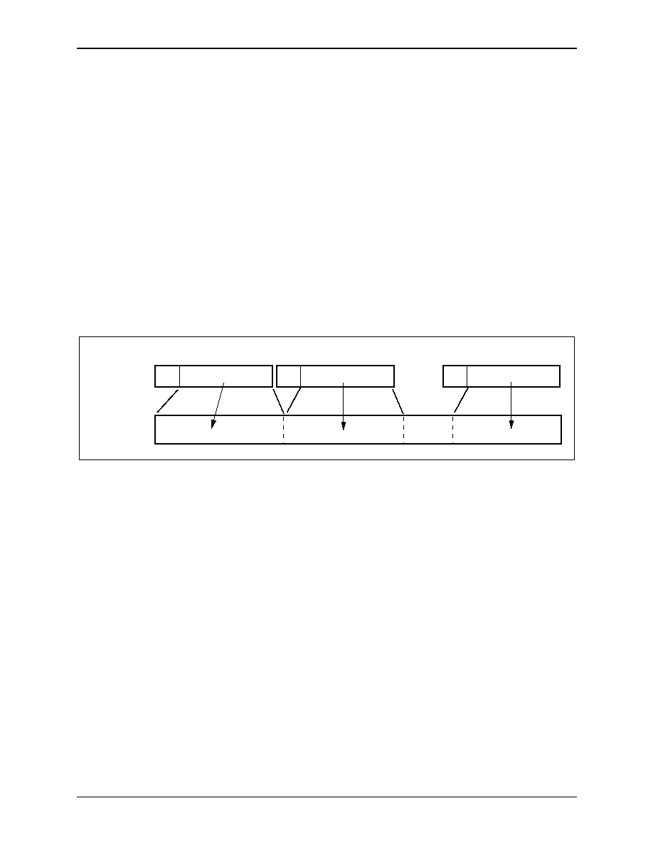
5.0 Reassembly Coprocessor
RS8234
5.3 CPCS-PDU Processing
ATM ServiceSAR Plus with xBR Traffic Management
5-8
Mindspeed Technologies
TM
28234-DSH-001-B
5.3 CPCS-PDU Processing
After the VCC has been identified via channel lookup, the reassembly
coprocessor performs the appropriate CPCS-PDU processing according to the
AAL_TYPE field in the reassembly VCC table.
The reassembly process is essentially the extraction and concatenation of
consecutive ATM cell payloads on a specific VCC to form a CPCS-PDU. This
processing is either reassembly into an AAL5 PDU, according to the specification
in ANSI T1.635, reassembly into an AAL3/4 PDU, or reassembly into a
transparent AAL0 PDU. The exact process is governed by the AAL type
described in detail in the subsections below.
Figure 5-6
illustrates the basic process function.
SETUP
Each active reassembly VCC must have a corresponding entry in the reassembly
VCC table to describe its state. At channel setup time -- either during system
initialization for Provisioned Virtual Connections (PVCs), or dynamically for
Switched Virtual Connections (SVCs) -- the host allocates a reassembly VCC
table entry and configures the VCC according to its provisioned or negotiated
characteristics. This includes the AAL in use, its assigned buffer pools and
allocation priority, as well as the associated segmentation VCC Index
(SEG_VCC_INDEX) for full duplex connections.
OPERATION
Once the reassembly process is activated, this RSM VCC table entry will be used
to track the current state of the connection and direct the RS8234 to perform
specific functions as described throughout this chapter.
Figure 5-6. CPCS-PDU Reassembly
CPCS-PDU
ATM Cells
(Hdr)
(Payload)
. . .
. . .
(For a
Specific VCC)
(Hdr)
(Payload)
(Hdr)
(Payload)
BOM Cell
EOM Cell
COM Cells . . .
100074_027
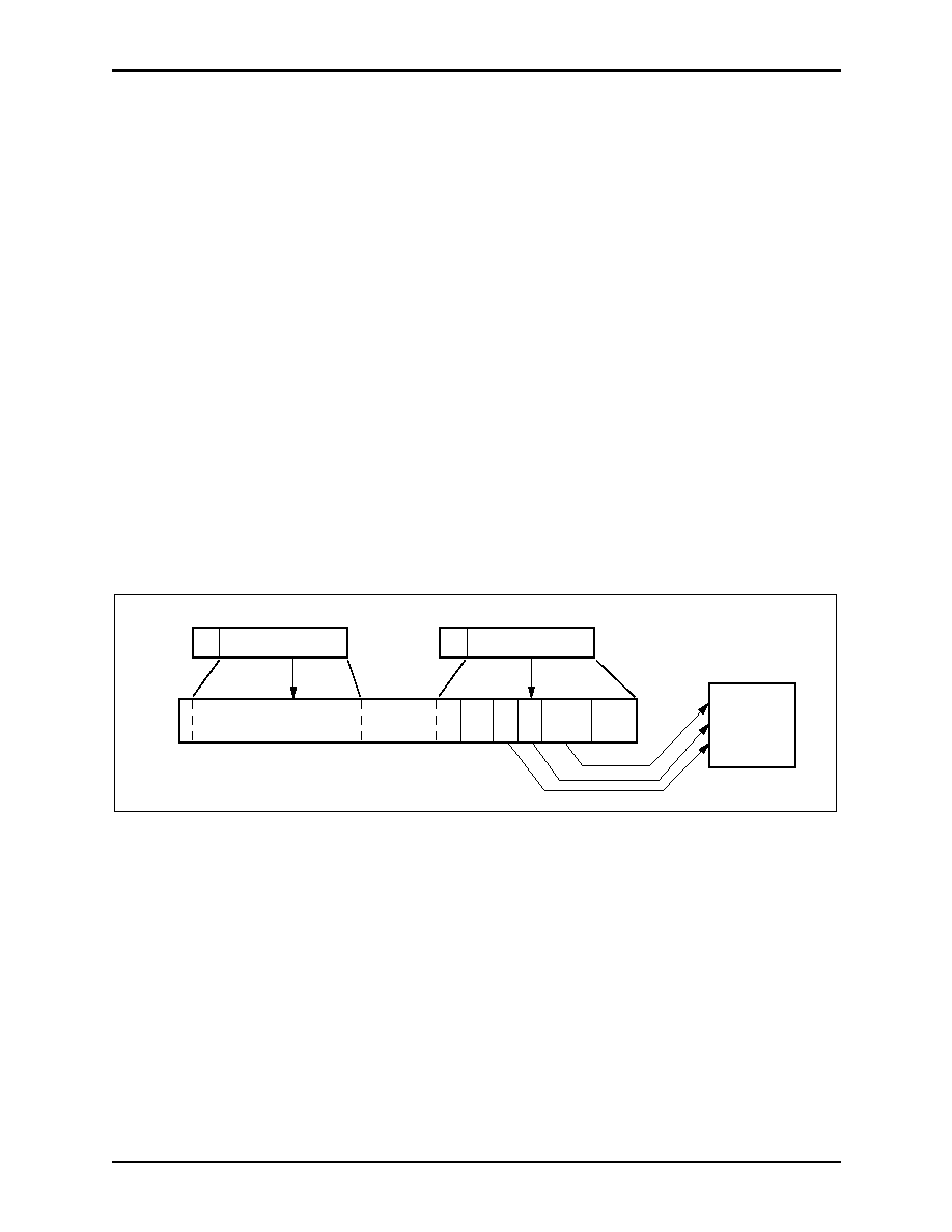
RS8234
5.0 Reassembly Coprocessor
ATM ServiceSAR Plus with xBR Traffic Management
5.3 CPCS-PDU Processing
28234-DSH-001-B
Mindspeed Technologies
TM
5-9
5.3.1 AAL5 Processing
Except for the EOM cell, all of the data within AAL5 cell payloads is user data.
The reassembly coprocessor writes all user data to memory as described in
Section 5.4
. The EOM cell contains both user data and CPCS-PDU overhead, and
delineates the end of an AAL5 PDU.
5.3.1.1 AAL5 COM
Processing
During reassembly of the PDU, the reassembly coprocessor calculates a CRC-32
value on the received AAL5 PDU, as well as counting the length of the PDU. The
CRC-32 value is collected in an accumulator, and the LENGTH value is collected
in a Length Counter. After each received cell is processed, the reassembly
coprocessor writes the CRC-32 and LENGTH values to the reassembly VCC state
table entry for that channel.
5.3.1.2 AAL5 EOM
Processing
During reassembly of the AAL5 PDU, certain bytes of the PDU other than user
data are written to a status queue entry for that PDU. The RSM coprocessor writes
these specific fields to the status queue entry:
�
UU information
�
the CPI field
�
the LENGTH field
Figure 5-7
illustrates these process functions.
Figure 5-7. AAL5 EOM Cell Processing -- Fields to Status Queue
. . .
. . .
. . .
ATM Cells
EOM Cell
AAL5 PDU
(User Data)
PAD
UU CPI LENGTH CRC-32
Status
Queue
Entry
100074_028
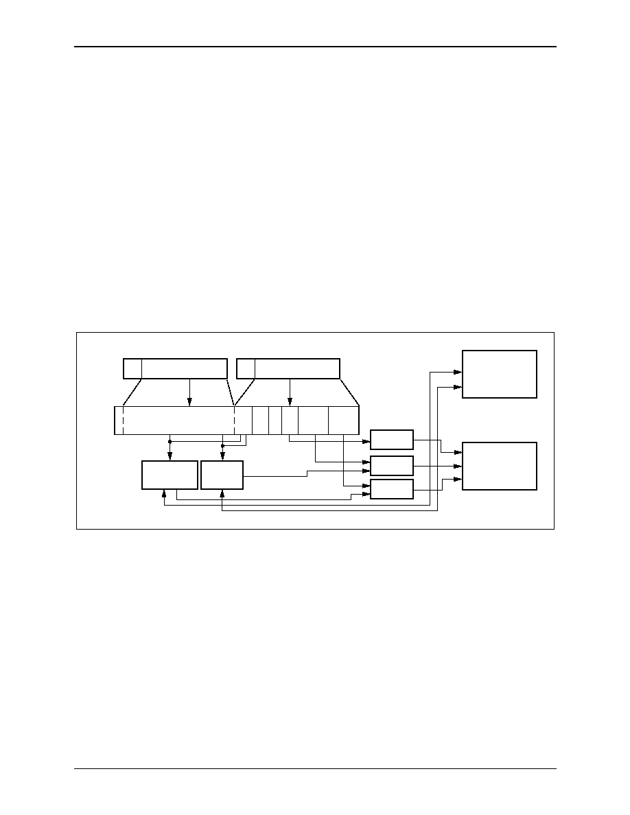
5.0 Reassembly Coprocessor
RS8234
5.3 CPCS-PDU Processing
ATM ServiceSAR Plus with xBR Traffic Management
5-10
Mindspeed Technologies
TM
28234-DSH-001-B
When the EOM cell is processed, the reassembly coprocessor performs the
following checks:
�
If the LENGTH field in the trailer of the AAL5 PDU is zero, the ABORT
bit in the status queue entry is set to a logic high.
�
Compares the calculated CRCREM value to the CRC-32 value in the
trailer of the AAL5 PDU. If different, the reassembly coprocessor sets the
CRC_ERROR bit in the status queue entry to a logic high.
�
Compares the value collected in the Length Counter to the value in the
LENGTH field in the trailer of the AAL5 PDU. If the number of Pad bytes
is less than zero or greater than 47, the PAD_ERROR bit in the status
queue entry is set to a logic high.
�
If the CPI field in the AAL5 trailer is not zero, the CPI_ERROR bit in the
status queue entry is set to a logic high.
NOTE:
All trailer information is written to the reassembly buffer.
Figure 5-8
illustrates these process functions.
The RS8234 reports all PDU termination events, with or without errors, in a
status queue entry for that channel. See
Section 5.6
for full details.
Figure 5-8. AAL5 Processing -- CRC and PDU Length Checks
. . .
(User Data)
CPI LENGTH
Status
Queue
Entry
EOM Cell
AAL5 PDU
PAD
ATM Cells
UU
RSM VCC
Table Entry
CRC-32
Accumulator
(Pad
Check)
(Compare)
(Not Null)
Length
Counter
CRC-32
100074_029

RS8234
5.0 Reassembly Coprocessor
ATM ServiceSAR Plus with xBR Traffic Management
5.3 CPCS-PDU Processing
28234-DSH-001-B
Mindspeed Technologies
TM
5-11
5.3.1.3 AAL5 Error
Conditions
The user can set a global variable for the reassembly coprocessor, RSM_CTRL0
(MAX_LEN), dictating maximum SDU delivery length. The maximum allowable
length, in bytes, of any AAL5 CPCS-PDU, including trailer and pad, is
During reassembly, this MAX_LEN value is checked to ensure that the PDU
under reassembly does not exceed the maximum SDU delivery length.
If the RS8234 receives a non-EOM cell, where
Early Packet Discard is performed.
The RS8234 reports this condition via a status queue entry, with the
LEN_ERROR and EPD status bits set. The AAL5_DSC_CNT counter is also
incremented. Refer to
Section 5.4.8
, for details on how this process is handled.
For each EOM cell where
the PDU is completed, with BA_ERROR status bit set.
min[RSM_CTRL0(MAX_LEN)
1024, 65568
�
TOT_PDU_LEN
48 > MAX_LEN
1024 (or 65568)
�
+
TOT_PDU_LEN
48 > MAX_LEN
1024 (or 65568)
�
+
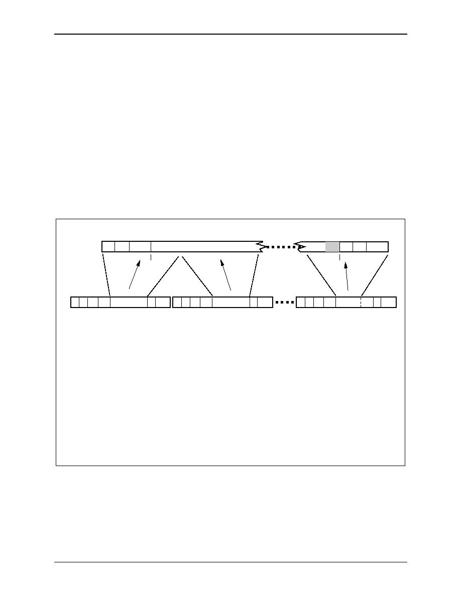
5.0 Reassembly Coprocessor
RS8234
5.3 CPCS-PDU Processing
ATM ServiceSAR Plus with xBR Traffic Management
5-12
Mindspeed Technologies
TM
28234-DSH-001-B
5.3.2 AAL3/4 Processing
The BOM cell contains the header information for the AAL3/4 PDU, and the
EOM cell contains the trailer information for the PDU. All of the other cell
payloads for that PDU contain user data. The reassembly coprocessor writes all
header, trailer, and user data to memory as described in
Section 5.4
. The EOM
cell contains both user data and CPCS-PDU overhead, and delineates the end of
an AAL3/4 PDU.
The BOM cell for a PDU will have the Segment Type (ST) field in the cell set
to
b10
, and the EOM cell will have the ST field set to
b01
. All COM cells will
have the ST field set to
b00
. An ST field value of
b11
indicates a Single Segment
Message (SSM), i.e., the cell holds all of a short PDU.
Figure 5-10
illustrates an AAL3/4 CPCS-PDU reassembled from the received
cell stream.
Figure 5-9. AAL3/4 CPCS-PDU Reassembly
AAL3/4 CPCS-PDU
<64 K
CPI Btag BASIZE
Header
Payload
PAD
PAD
AL Etag Length
Trailer
Received Cells
(44 bytes)
H ST SN MID
Information
LI CRC
H ST SN MID
LI CRC
H ST SN MID
LI CRC
100074_030
AAL3/4 PDU fields:
CPI = Common Part Indicator. In AAL3/4, initially set to all 0s.
Btag = Beginning Tag. Has the same identifying number as the Etag field. When the receiver reassembles a long PDU,
these tags help identify that cells are from the same PDU.
BASIZE= Buffer Allocation size. Tells the receiver how large the buffer allocation must be to receive and reassemble this PDU.
AL = Aligns the trailer to fit a 4-byte word.
Etag = Ending Tag. (See Btag above.)
Length = Contains the exact size of the PDU's payload.
AAL3/4 ATM cell fields:
ST = Segment Type. 10 = beginning of message, 00 = continuation of message, 01 = end of message, and 11 = single
segment message.
SN = Sequence Number. The cell number sequence within the PDU. Cycles through 16 values.
MID = Message Identification. Allows many long SDUs to be multiplexed onto a single stream of cells. The reassembly
processor sorts cells by MID and reassembles PDUs from cells with the same MID.
LI = Length Indication. Dictates the length of pad of the SDU, to a multiple of four octets.
CRC = A CRC check of the 48-byte ATM cell payload.

RS8234
5.0 Reassembly Coprocessor
ATM ServiceSAR Plus with xBR Traffic Management
5.3 CPCS-PDU Processing
28234-DSH-001-B
Mindspeed Technologies
TM
5-13
5.3.2.1 AAL3/4 Per-Cell
Processing
The following processing steps and checks occur on a per-cell basis:
�
If the CRC10_EN bit in the AAL3/4 Head VCC table entry is a logic high,
the CRC10 field in the cell is checked. If in error, the SAR increments the
CRC10_ERR counter in the VCC Head table entry, and discards the cell.
�
The MID field value is checked against active MID values specified by the
MID_BITS and MID0 fields in the AAL3/4 Head VCC table entry. If
invalid, the SAR discards the cell, and increments the MID_ERR counter
in the VCC Head table entry.
�
If the cell is an EOM cell and LI = 63, the SAR writes a status queue entry
with ABORT bit set, CPCS_LENGTH=0, and BD_PNTR pointing to the
partially reassembled PDU.
�
If the LI_EN bit in the AAL3/4 Head VCC table entry is a logic high, the
LI field is checked, and the following error detection and error processing
is done:
� If the cell received is a BOM, and LI
44; the SAR discards the cell,
and increments the LI_ERR counter in the VCC Head table entry.
� If the cell received is a COM, and LI
44; the SAR discards the cell,
and terminates the current CPCS-PDU. The SAR also writes a status
queue entry with the LI_ERROR bit set, the CPCS_LENGTH = 0, and
BD_PNTR pointing to the partially reassembled PDU. The SAR also
increments the LI_ERR counter in the VCC Head table entry.
� If the cell received is an EOM, and (LI < 4 or LI > 44); the SAR
discards the cell, and terminates the current CPCS-PDU. The SAR also
writes a status queue entry with the LI_ERROR bit set, the
CPCS_LENGTH = 0, and BD_PNTR pointing to the partially
reassembled PDU. The SAR also increments the LI_ERR counter in the
VCC Head table entry.
� If the cell received is an SSM, and (LI < 8 or LI > 44); the SAR
discards the cell, and increments the LI_ERR counter in the VCC Head
table entry.
�
If the ST_EN bit in the AAL3/4 Head VCC table entry is a logic high, the
ST field in the cell is checked. The NEXT_ST field in the VCC entry is
used for this check. A value of "01" in the NEXT_ST field indicates that
the SAR was expecting a BOM/SSM cell. An "00" value indicates that the
SAR was expecting a COM/EOM cell. The following error detection and
error processing is done:
� If the cell received is a BOM, and the SAR was expecting a COM or
EOM; the SAR terminates the current CPCS-PDU, and writes a status
queue entry with the ST_ERROR bit set, the CPCS_LENGTH = 0, and
the BD_PNTR pointing to the partially reassembled PDU. The SAR
also increments the BOM_SSM_ERR counter in the VCC Head table
entry, and starts a new CPCS-PDU with the current BOM cell.
� If the cell received is an SSM, and the SAR was expecting a COM or
EOM; the SAR terminates the current CPCS-PDU, and writes a status
queue entry with the ST_ERROR bit set, the CPCS_LENGTH =0, and
the BD_PNTR pointing to the partially reassembled PDU. The SAR
also increments the BOM_SSM_ERR counter in the VCC Head table
entry, and processes the current cell as a valid CPCS-PDU.
� If the cell received is a COM, and the SAR was expecting a BOM or
SSM; the SAR discards the cell.

5.0 Reassembly Coprocessor
RS8234
5.3 CPCS-PDU Processing
ATM ServiceSAR Plus with xBR Traffic Management
5-14
Mindspeed Technologies
TM
28234-DSH-001-B
� If the cell received is an EOM, and the SAR was expecting a BOM or
SSM; the SAR discards the cell, and increments the EOM_ERR
counter in the VCC Head table entry.
�
If the SN_EN bit in the AAL3/4 Head VCC table entry is a logic high, the
SN field in the cell is checked. If the cell received is an COM or EOM, and
the SN field does not equal the NEXT_SN field in the VCC Table entry;
the SAR discards the cell, terminates the current CPCS-PDU, and writes a
status queue entry with the SN_ERROR bit set, CPCS_LENGTH = 0, and
the BD_PNTR pointing to the partially reassembled PDU. The SAR also
increments the SN_ERR counter in the VCC Head table entry.
5.3.2.2 AAL3/4
Additional BOM/SSM
Processing
The RS8234 performs the following additional checks and functions on each
BOM or SSM cell received:
�
When a BOM cell is received for an AAL3/4 CPCS-PDU (i.e., with ST
field set to
b10
), the RS8234 checks if the CPI_EN bit in the RSM
AAL3/4 Head VCC table entry is set to a logic high. If so, the CPI field in
the received cell is checked for a zero value. If not a zero value, the
RS8234 treats this as an error condition and discards the cell, terminates
the current CPCS-PDU, writes a status queue entry with the CPI_ERROR
bit set, and the CPCS_LENGTH and BD_PNTR fields set to zero. Cells up
to and including the next EOM are discarded.
�
The RS8234 also checks if the BAH_EN bit in the RSM AAL3/4 Head
entry is set to a logic high. If so, it checks if the BASIZE field in the
CPCS-PDU header is less than 37 octets, and if so, the RS8234 discards
the current cell, terminates the current CPCS-PDU, and writes a status
queue entry with the BA_ERROR bit set, and the CPCS_LENGTH and
BD_PNTR fields set to zero. Cells up to and including the next EOM are
discarded.
�
If the CPI and BASIZE fields are correct in the BOM cell, the RS8234
copies the BASIZE and BTAG fields into the VCC table entry for that
MID, and sets the NEXT_ST and NEXT_SN values in the VCC table
entry. It also writes the CPCS-PDU header into the data buffer.
�
If the LI field in the SAR-PDU > (BASIZE+7), the SAR discards the cell,
terminates the CPCS-PDU, and writes a status queue entry with the
LEN_ERROR bit set and CPCS_LENGTH = zero.
5.3.2.3 AAL3/4
Additional COM
Processing
The RS8234 performs the following additional checks and functions on each
COM cell received:
�
The RS8234 checks if the sum of the LI fields for the CPCS-PDU are
greater than (BASIZE + 7). If so, the RS8234 discards the cell, terminates
the CPCS-PDU, and writes a status queue entry with the LEN_ERROR bit
set high, CPCS_LENGTH set to zero, and BD_PNTR pointing to the
partially reassembled PDU.

RS8234
5.0 Reassembly Coprocessor
ATM ServiceSAR Plus with xBR Traffic Management
5.3 CPCS-PDU Processing
28234-DSH-001-B
Mindspeed Technologies
TM
5-15
5.3.2.4 AAL3/4
Additional EOM/SSM
Processing
Upon termination of a CPCS-PDU, the RS8234 performs the following additional
checks and functions on each EOM or SSM cell received:
�
The Length field in the CPCS-PDU trailer is written to the
CPCS_LENGTH field of a RSM status queue entry written for the VCC.
�
The RS8234 performs a Pad length check to see if the sum of all LIs for
the CPCS-PDU - LENGTH - 8 = [0 to 3] octets. If in error, it sets the
PAD_ERROR bit in the status queue entry.
�
The RS8234 performs a Modulo 32 bit check. If the sum of all LIs for the
CPCS-PDU is not modulo 32 bit, the SAR sets the MOD_ERROR bit in
the status queue entry.
�
If the Alignment (AL) field in the CPCS-PDU trailer is not all zeros, it sets
the AL_ERROR bit in the status queue entry.
�
If the BTAG field in the RSM VCC table entry does not match the ETAG
field in the CPCS-PDU trailer, it sets the TAG_ERROR bit in the status
queue entry.
�
The RS8234 checks the BAT_EN bit in the AAL3/4 Head VCC table entry.
If BAT_EN is high, it compares the BASIZE field to the Length field in
the CPCS-PDU trailer. If not a match, it sets the BA_ERROR bit in the
status queue entry. If BAT_EN is low, it checks if the Length field is >
BASIZE; and if so, sets the BA_ERROR bit in the status queue entry.
�
The RS8234 writes the AAL3/4 CPCS-PDU trailer to the data buffer.
5.3.2.5 AAL3/4 MIB
Counters
Whenever an AAL3/4 MIB counter rolls over to all zeros, the RS8234 writes a
RSM status queue entry with the CNT_ROVR bit set to a logic high, and the
HEAD_VCC_INDEX field pointing to the AAL3/4 Head VCC entry which
contains the rolled-over counter. This processing step takes place for the
CRC10_ERR, MID_ERR, LI_ERR, SN_ERR, BOM_SSM_ERR, and
EOM_ERR counters.
5.3.3 AAL0 Processing
AAL0 is a transparent adaptation layer, allowing for pass-through of raw data
cells during CPCS-PDU processing. AAL0 channels are intended to be used for
AAL proprietary adaptation layers.
5.3.3.1 Termination
Methods
The RS8234 provides two methods of terminating an AAL0 PDU: Cell Count
EOM and PTI termination.
The TCOUNT field in the RSM VCC state table entry determines the method
for each VCC.
�
If TCOUNT = nonzero, Cell Count EOM PDU termination is enabled.
PDUs will terminate when a fixed number of cells (TCOUNT) have been
received. CCOUNT must be initialized to a value of one in this mode.
�
If TCOUNT = zero, then PTI termination is enabled. In this case, a
received cell with PTI[0] set to one indicates the end of the AAL0
message. The total maximum allowable length of an AAL0 PDU in this
mode is (CCOUNT * 2) bytes.
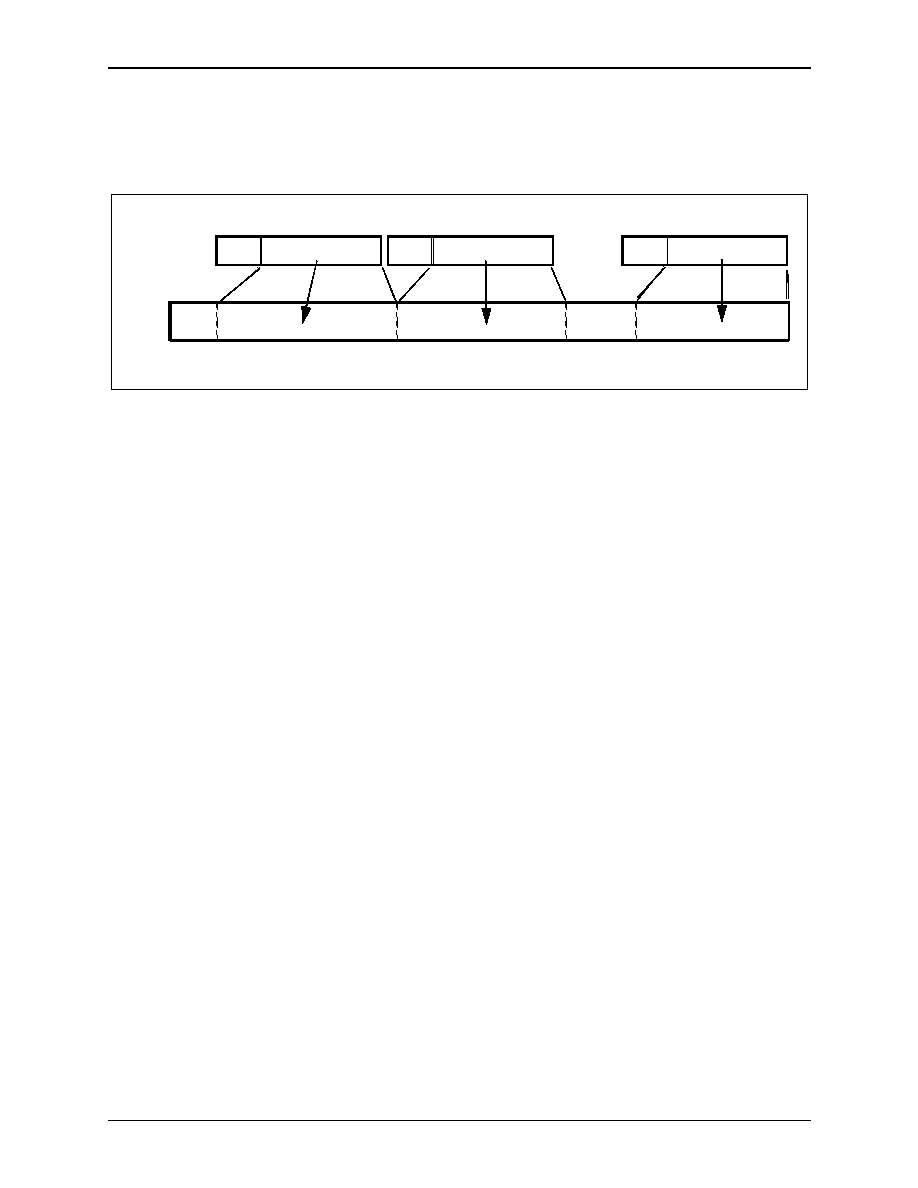
5.0 Reassembly Coprocessor
RS8234
5.3 CPCS-PDU Processing
ATM ServiceSAR Plus with xBR Traffic Management
5-16
Mindspeed Technologies
TM
28234-DSH-001-B
Figure 5-10
provides an illustration of this.
The RS8234 reports all PDU termination events, with or without errors, in a
Status Queue entry for that channel. See
Section 5.6
.
5.3.3.2 AAL0 Error
Conditions
If the RS8234 receives a non-EOM cell in PTI termination mode, where
EPD is performed. The RS8234 reports this condition via a status queue entry,
with the LEN_ERROR and EPD status bits set. Refer to
Section 5.4.8
, for details
on how this process is handled.
For each EOM cell where
the PDU is completed, with BA_ERROR status bit set.
The RS8234 processes error conditions for AAL0 (such as free buffer queue
underflow, status queue overflow, and per-channel buffer firewall), in the same
way as AAL5 CPCS-PDUs are processed.
5.3.4 ATM Header Processing
ATM level CI and CLP are mapped to the CPCS-PDU status queue entry in the
following manner:
�
LP: value of the ATM Header CLP bit ORed across all cells in a
CPCS-PDU.
�
CI_LAST: value of ATM Header PTI[1] bit in last cell of CPCS-PDU.
�
CI: value of ATM Header PTI[1] bit ORed across all cells in a CPCS-PDU.
Figure 5-10. AAL0 PTI PDU Termination
(Payload)
(Payload)
(Payload)
. . .
. . .
. . .
. . .
ATM Cells
AALO PDU
(Hdr)
PTI[0]=0
(Hdr)
PTI[0]=0
(Hdr)
PTI[0]=1
(EOM Cell)
100074_031
TOT_PDU_LEN
48 > CCOUNT
2
�
+
TOT_PDU_LEN
48 > CCOUNT
2
�
+

RS8234
5.0 Reassembly Coprocessor
ATM ServiceSAR Plus with xBR Traffic Management
5.3 CPCS-PDU Processing
28234-DSH-001-B
Mindspeed Technologies
TM
5-17
5.3.5 BOM Synchronization Signal
The STAT[1:0] output pins can be programmed to provide an indication that a
BOM cell is being written across the PCI bus. Additional external circuitry could
snoop the BOM cell for a service level protocol header, and perform appropriate
lookup as the CPCS-PDU is being reassembled. To configure the STAT pins, set
the STATMODE field in the CONFIG0 register to 0x00. The STAT output truth
table illustrated in
Table 5-2
.
The STAT output pins are valid during a SAR PCI master write address cycle.
External circuitry would detect a BOM cell transfer by detecting a logic high on
either STAT pin during a SAR PCI master write address cycle. External circuitry
can then snoop the subsequent data cycles of the BOM cell transfer to extract the
appropriate protocol overhead.
Table 5-2. STAT Output Pin Values for BOM Synchronization
STAT[1]
STAT[0]
NOT BOM
0
0
AAL5 BOM
0
1
AAL0 BOM
1
0
NOT USED
1
1

5.0 Reassembly Coprocessor
RS8234
5.4 Buffer Management
ATM ServiceSAR Plus with xBR Traffic Management
5-18
Mindspeed Technologies
TM
28234-DSH-001-B
5.4 Buffer Management
Once CPCS-PDU processing has been implemented, the cell payloads are written
to data buffers. Each channel retrieves the location of its buffers from one of
32 free buffer queues. The reassembly coprocessor tracks the location of the
buffers from the VCC table entry for that channel.
NOTE:
The process cycle time of a read transaction across the PCI bus is much
longer than a write transaction, due to the PCI bus being held in a busy
state while the remote processor accesses and processes the read request.
Therefore, to speed up processing flow during reassembly, the RS8234
uses only control and status writes across the PCI bus between host and
local systems.
Data buffers are supplied according to the mechanisms detailed below.
5.4.1 Host vs. Local Reassembly
Data buffers can reside in both host and SAR shared memory. The majority of
user data traffic should be reassembled in host memory. SAR shared memory
reassembly is intended for low bandwidth management and control functions,
such as OAM and Signaling. This allows an optional local processor to off-load
these network management functions from the host, focusing host processing
power on the user application.
RS8234
5.0 Reassembly Coprocessor
ATM ServiceSAR Plus with xBR Traffic Management
5.4 Buffer Management
28234-DSH-001-B
Mindspeed Technologies
TM
5-19
5.4.2 Scatter Method
The RS8234 uses an intelligent scatter method to write cell payload data to host
memory. During reassembly to host memory, the reassembly coprocessor uses the
DMA coprocessor to control the scatter function. The reassembly coprocessor
controls the incoming DMA block during scatter DMA to host memory.
Four data structures are maintained as illustrated in
Figure 5-11
: two in the
host memory, one in SAR shared memory, and one in internal memory. The
linked cell buffers (HCELL_BUFF) and reassembly buffer descriptors reside in
host memory, and the free buffer queues (HFR_BUFF_QU) reside in SAR shared
memory. The free buffer queues also have an associated free buffer queue base
table. This table is in internal memory. The RS8234 allows for up to
32 independent free buffer queues.
Figure 5-11. Host and SAR Shared Memory Data Structures for Scatter Method
HOST
SAR-Shared
Cell buffers
Buffer Descriptors
Free Buffer Queues
Free Buffer Queue
Base Table
(Inside the RS8234)
100074_032

5.0 Reassembly Coprocessor
RS8234
5.4 Buffer Management
ATM ServiceSAR Plus with xBR Traffic Management
5-20
Mindspeed Technologies
TM
28234-DSH-001-B
5.4.3 Free Buffer Queues
The free buffer queue structure consists of a free buffer queue base table, two
base address registers, RSM_FQBASE(FBQ0_BASE and FBQ1_BASE), and the
corresponding free buffer queues.
The reassembly VCC table entry for any channel contains two 5-bit fields:
BFR0 and BFR1. These fields identify the free buffer queues that have been
assigned to this channel by the host during initialization of the VCC table entry.
BFR0 contains the BOM free buffer queue number, and BFR1 contains the COM
free buffer queue number. Typically, the BFR0 number is for free buffer queues
0-15, and the BFR1 number is for free buffer queues 16-31.
The free buffer queue is configured in two banks. Bank 0 contains free buffer
queues 0-15, and Bank 1 contains free buffer queues 16-31.
The user can set BFR0 = BFR1, to disable this two-tier buffer structure.
Depending on the type of arriving cell (whether BOM or COM), the
corresponding BFRx buffer number is used as an index to the appropriate free
buffer queue base table entry.
The base addresses for these banks are in RSM_FQBASE(FBQ0_BASE and
FBQ1_BASE). The reassembly coprocessor calculates the address of the first
entry for any of the 32 free buffer queues as follows:
FBQx_BASE + [(size of each free buffer queue) x BFRx MOD 16]
Each of the 32 free buffer queues is a circular queue whose entries are
sequentially read by the SAR. The reassembly coprocessor calculates the index
for each sequential read as follows:
(index of first entry for the queue) + [(READ index pointer) x (size of
each free buffer queue entry)]
The READ field in the base table entry for any free buffer queue is the current
READ index pointer, and is continually updated with each read of that queue.
Each free buffer queue entry contains a pointer to a buffer descriptor
(BD_PNTR), and a pointer to a data buffer (BUFFER_PNTR); and when the free
buffer queue entry is read it returns those pointers.
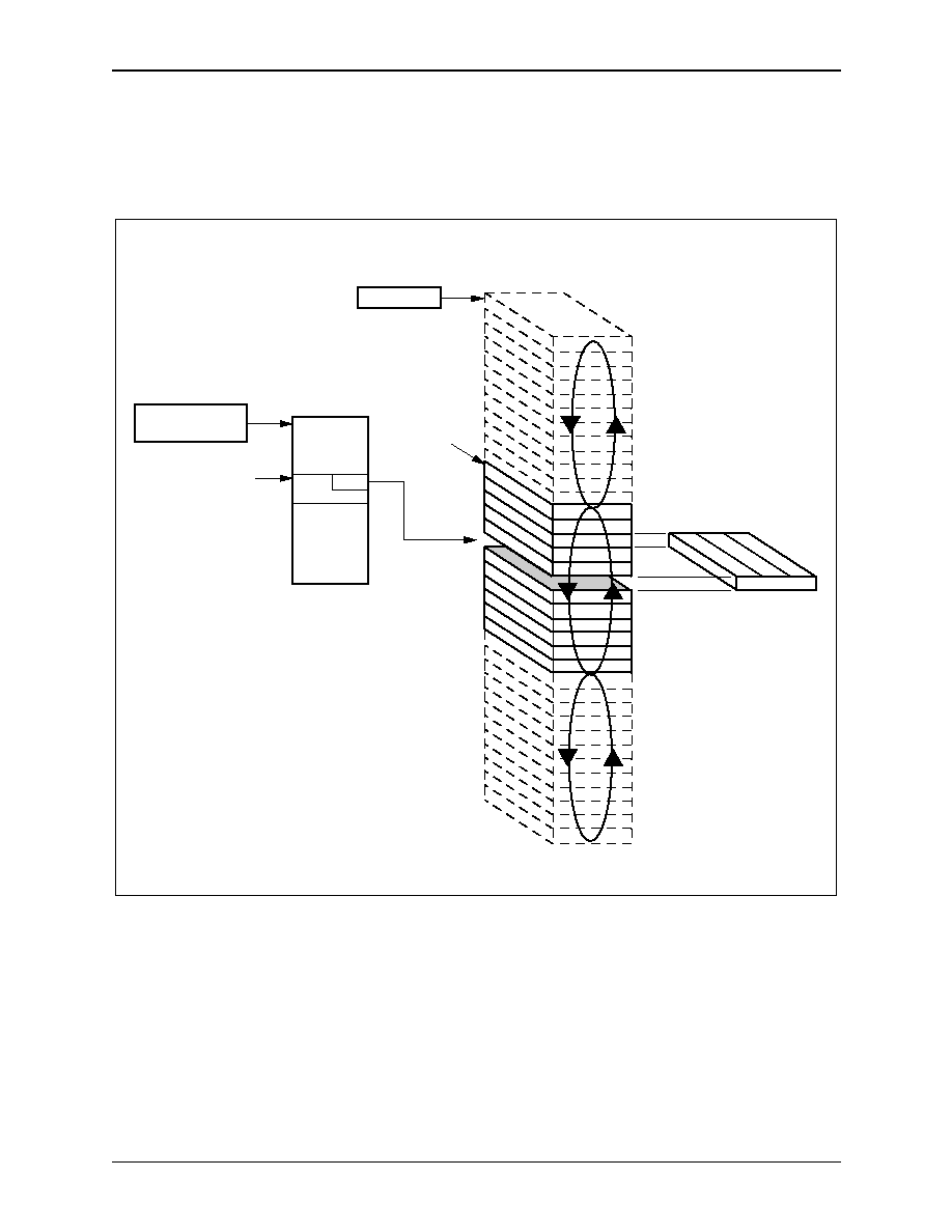
RS8234
5.0 Reassembly Coprocessor
ATM ServiceSAR Plus with xBR Traffic Management
5.4 Buffer Management
28234-DSH-001-B
Mindspeed Technologies
TM
5-21
Figure 5-12
illustrates this structure. Refer to
Chapter 3.0
for more
information on the operation of the Free Buffer Queue.
Figure 5-12. Free Buffer Queue Structure
BUFFER_PNTR
BD
_PN
TR
RSM_FBQ_QU0
0x1100
BFRx
(BFR0 or BFR1)
FBQ Base Table
(Internal SRAM)
[BFRx x
(Global size
of FBQ)]
READ
(16 Free Buffer Queues
in Each Bank)
Free Buffer Queue
Bank 0 or 1
(SAR-Shared Memory)
FBQx_BASE
100074_033

5.0 Reassembly Coprocessor
RS8234
5.4 Buffer Management
ATM ServiceSAR Plus with xBR Traffic Management
5-22
Mindspeed Technologies
TM
28234-DSH-001-B
5.4.4 Linked Data Buffers
After the free buffer queue has returned pointers to a buffer descriptor and a cell
buffer, the reassembly coprocessor writes payload data to the buffer.
The linked cell buffers contain the payload portions of the ATM cells. The
buffers do not contain any control information. A pointer in a separate buffer
descriptor structure links the buffers.
Thus, the pointer in the free buffer queue (BD_PNTR) points to a buffer
descriptor, which has a pointer (BUFF_PTR) pointing to a buffer. The use of this
buffer locating mechanism offers a layer of indirection in buffer assignment that
maximizes system architecture flexibility.
Figure 5-13
illustrates this structure.
The data buffers are linked by a pointer (NEXT_PNTR) in the first word of
the buffer descriptor, which is written by the reassembly coprocessor when the
current buffer is completed. The host writes the second word of the buffer
descriptor to point to the next associated data buffer. The link pointer of the last
buffer descriptor in a chain is written to NULL.
The link pointer (NEXT_PNTR) is not written if the LNK_EN bit in the RSM
VCC table entry for that channel is a logic low.
NOTE:
Only the data buffers are affected by big/little endian processing. The
buffer control structures (i.e., the buffer descriptors, free buffer queue base
table, and free buffer queues) are the same in both big and little endian
modes.
Figure 5-13. Data Buffer Structures
BUFF_PTR
NEXT_PTR
BUFF_PTR
NEXT_PTR
BUFF_PTR
NULL
Buffer Descriptors
(Host Memory)
Buffers
(Host Memory)
100074_034
NOTE(S):
No user fields in buffers - payload data only.

RS8234
5.0 Reassembly Coprocessor
ATM ServiceSAR Plus with xBR Traffic Management
5.4 Buffer Management
28234-DSH-001-B
Mindspeed Technologies
TM
5-23
5.4.5 Initialization of Buffer Structures
Before operation of the reassembly coprocessor is enabled, the host must initialize
these buffer structures. The initialization in this section assumes that the firewall
function is disabled (i.e., RSM_FQCTRL(FBQ0_RTN) = 0), and therefore, all
free buffer queue entries are two words.
5.4.5.1 Buffer
Descriptors
In every buffer descriptor entry, write the pointer to an available data buffer in the
BUFF_PTR field. This assigns every data buffer to its own buffer descriptor.
5.4.5.2 Free Buffer
Queue Base Table
Allocate the size (in number of entries) of each of the 32 free buffer queues in the
RSM_FQCTRL register, (FBQ_SIZE) field, based on these values:
00 = 64
01 = 256
10 = 1,024
11 = 4,096
Initialize the free buffer queue update INTERVAL, i.e., how many buffers are
taken off the free buffer queue before the RS8234 writes the current READ index
pointer to host memory. This is written to RSM_FQCTRL(FBQ_UD_INT).
Initialize the FORWARD, READ, UPDATE, and EMPT fields in each free
buffer queue base table entry to zeroes.
Initialize the READ_UD_PTR field in each base table entry with the
appropriate address.
Write the appropriate length (in bytes) for the data buffers in that queue in the
LENGTH field of each free buffer queue base table entry.
Initialize BFR_LOCAL and BD_LOCAL to the appropriate host/SAR shared
memory locations. Normally, both structures are in host memory.
5.4.5.3 Free Buffer
Queue Entries
Write the base addresses of free buffer queues Banks 0 and 1 in RSM_FQBASE
(FBQ0_BASE and FBQ1_BASE).
For each allocated free buffer queue entry, write the BD_PNTR and
BUFFER_PTR fields corresponding to the buffer and buffer descriptor pair. Also
write the VLD bit to a logic high.
For each unallocated free buffer queue entry, write the VLD bit to a logic low.
5.4.5.4 Other
Initialization
The user can globally disable free buffer underflow protection by setting
RSM_CTRL(RSM_FBQ_DIS) to a logic high.

5.0 Reassembly Coprocessor
RS8234
5.4 Buffer Management
ATM ServiceSAR Plus with xBR Traffic Management
5-24
Mindspeed Technologies
TM
28234-DSH-001-B
5.4.6 Buffer Allocation
The reassembly coprocessor performs buffer allocation when a new channel is
being reassembled, or when a buffer on an existing channel in process of being
reassembled, is full.
The reassembly coprocessor reads the appropriate free buffer queue base table
entry and free buffer queue entry. If the VLD bit is a logic low, a queue empty
condition has occurred. (The processing of this condition is described in
Section 5.4.7
.) If the VLD bit is a logic high, the reassembly coprocessor uses the
assigned buffer to store payload data.
The VLD bit is then written to a logic low without corrupting the BD_PNTR
value. The READ index pointer and UPDATE counter are incremented. If the
UPDATE counter equals RSM_FQCTL(FBQ_UD_INT), then the READ index
pointer is written to the location pointed to by READ_UD_PNTR, and the
UPDATE counter is reset to zero.
When the host wants to return a buffer to a free buffer queue, the host WRITE
index pointer is compared to the RS8234 READ index pointer located at
READ_UD_PNTR. If the WRITE index pointer + one is equal to the READ
index pointer, an overflow condition has been detected and further processing is
halted. Otherwise, the host writes and updates the free buffer queue entry with a
new buffer pointer, buffer descriptor pointer, and VLD bit set to a logic high. The
host then increments its WRITE index pointer.
5.4.7 Error Conditions
An empty condition occurs when a buffer is needed and there are no available
buffers in the free buffer queue. If the BFR1 queue is empty and BFR1 does not
equal BFR0, then the RSM coprocessor checks the BFR0 queue before declaring
an empty condition.
If an empty condition occurs after the first buffer of a CPCS-PDU is written,
the reassembly coprocessor will perform early packet discard on the channel and
write a status queue entry with the EPD and free buffer queue Underflow (UNDF)
bits set to a logic high. EPD functions are described in
Section 5.4.8
. Also, if a
buffer queue empty condition initially occurs at the beginning of a BOM cell, a
status queue entry is written with UNDF set to a logic high and BD_PNTR null.
In both cases, the RSM_HF_EMPT bit is set in the HOST_ISTAT1 and
LP_ISTAT1 registers if the BD_LOCAL bit is a logic low in the free buffer queue
base table, or the RSM_LF_EMPT bit is set if BD_LOCAL is a logic high.
All cells of a PDU up to and including the next EOM cell are discarded. Upon
receiving a BOM or SSM cell, the reassembly coprocessor checks the queue
indicated by BFR0 for a valid free buffer. If a free buffer exists, the RSM
coprocessor stores the cell in the assigned buffer.
For AAL5 channels, the AAL5_DSC_CNT counter is incremented for each
CPCS_PDU discarded during this error condition.
Channels that have outstanding buffers from an empty queue are not affected
until they need a new buffer. Once the host has written more free buffers on the
queue with VLD bit set to a logic high, the reassembly coprocessor will
automatically recover from the empty condition.

RS8234
5.0 Reassembly Coprocessor
ATM ServiceSAR Plus with xBR Traffic Management
5.4 Buffer Management
28234-DSH-001-B
Mindspeed Technologies
TM
5-25
5.4.8 Early Packet Discard
The packet discard feature provides a mechanism to discard complete or partial
CPCS-PDUs, based upon service discard attributes or error conditions.
5.4.8.1 General
Description
The EPD feature performs these basic functions:
�
Halts reassembly of the CPCS-PDU marked for discard until the next
BOM cell and the error condition has cleared.
�
Writes a status queue entry with the EPD bit set and other appropriate
STATUS and PDU_CHECKS bits set, based on the reason for the discard.
5.4.8.2 Frame Relay
Packet Discard
The frame relay discard attribute is contained in the BOM cell of a CPCS-PDU. If
the FRD_EN bit in the RSM VCC table is a logic high, the frame relay packet
discard function for that VCC is enabled, and the functions below are performed:
�
When the reassembly coprocessor receives a BOM cell on a VCC with this
feature enabled, it checks the 1-bit DE field in the frame relay header. If
this bit is a logic high, and the channel priority (the DPRI in the RSM VCC
table) is less than or equal to the global priority, RSM_CTRL (GDIS_PRI),
the RSM coprocessor discards the cell, marks the rest of the packet for
discard, and increments the SERV_DIS counter in the VCC table. All cells
on that channel up to the next BOM are discarded.
�
If the SERV_DIS counter rolls over, the CNT_ROVR bit in the next status
entry for this channel is set to a logic high. The CNT_ROVR bit in the
VCC table holds this flag information until a status is sent.
5.4.8.3 CLP Packet
Discard
If the CLPD_EN bit in the RSM VCC table is a logic high, the Cell Loss Priority
packet discard function for that VCC is enabled, and the following functions
below are performed:
�
When the RSM coprocessor receives a cell and this function is enabled, it
checks the 1-bit CLP field in the ATM header. If this bit is a logic high,
and the channel priority is less than or equal to the global priority,
RSM_CTRL (GDIS_PRI), the RSM coprocessor discards the cell, marks
the rest of the packet for discard, and increments the SERV_DIS counter in
the VCC table. All cells on that channel up to the next BOM are discarded.
�
If the SERV_DIS counter rolls over, the CNT_ROVR bit in the next status
entry for this channel is set to a logic high. The CNT_ROVR bit in the
VCC table holds this flag information until a status is sent.
5.4.8.4 LANE-LECID
Packet Discard--Echo
Suppression on Multicast
Data Frames
The system designer can use this feature to discard superfluous traffic on the
ATM network caused by LAN Emulation Clients (LECs) transmitting multicast
frames, i.e., point-to-multipoint Emulated LAN traffic.
If the LECID_EN bit in the RSM VCC Table is a logic high, the
LANE-LECID discard function for that VCC is enabled, and the functions below
are performed:
�
The DPRI field is used as an index into the LECID table. This allows
support for up to 32 LECIDs, each a unique identifier for a single LAN
Emulation Client.
�
When the RSM coprocessor receives a BOM cell with this function
enabled, it checks the 16-bit LECID field in the LANE header against the
value in the LECID table. If a match occurs, the RSM coprocessor discards
the cell, marks the rest of the packet for discard and increments the
SERV_DIS counter in the VCC Table.
�
If the SERV_DIS counter rolls over, the CNT_ROVR bit in the next status

5.0 Reassembly Coprocessor
RS8234
5.4 Buffer Management
ATM ServiceSAR Plus with xBR Traffic Management
5-26
Mindspeed Technologies
TM
28234-DSH-001-B
entry for this channel will be set to a logic high. The CNT_ROVR bit in the
VCC Table holds this flag information until a status is sent.
5.4.8.5 DMA FIFO Full
The purpose of this function is to allow a graceful recovery from an incoming
DMA FIFO full condition. Without this function the reassembly coprocessor is
stalled when the FIFO is full, until recovery from the full condition. This causes
the cells to be dropped indiscriminately on the upstream side of the reassembly
block without any record of which VCCs the cells belonged to. Upon recovery
from the full condition, cells belonging to corrupted PDUs continue to be
processed, which wastes PCI bandwidth during the recovery phase. This function
provides for a more efficient use of host and SAR resources by allowing the
reassembly block to process and drop cells during the full condition.
The reassembly block will mark all channels that receive a cell during the full
condition for subsequent early packet discard. Upon recovery from the full
condition, the reassembly block performs early packet discard on the appropriate
channels as cells are received on those channels. In addition, cells will continue to
be dropped on each channel until after an EOM cell is received for that channel.
Early packet discard processing is delayed until recovery from the full condition,
since the status entry also requires the use of the incoming DMA FIFO.
This function is enabled by setting the FF_DSC bit in each VCC entry to a
logic high.
The user may want to disable this function if the free buffers, buffer
descriptors, and RSM status queues reside in SAR shared memory.
Similarly, if RSM_CTRL1(OAM_QU_EN) is a logic high, RSM_CTRL1
(OAM_FF_DSC) should be set to a logic high.
The user may want to disable this function if the global OAM buffers, buffer
descriptors, and status queues reside in SAR shared memory.
Early packet discard due to a FIFO full condition is indicated by the FFPD bit
in the RSM status queue entry being a logic high.

RS8234
5.0 Reassembly Coprocessor
ATM ServiceSAR Plus with xBR Traffic Management
5.4 Buffer Management
28234-DSH-001-B
Mindspeed Technologies
TM
5-27
5.4.8.6 AAL3/4 Early
Packet Discard
Processing
The RS8234 performs EPD for AAL3/4 CPCS-PDUs with these steps:
�
Sets the appropriate error bit in the PDU_CHECKS field for a new RSM
Status Queue entry.
�
Sets the CPCS_LENGTH field to zero.
�
Sets the BD_PNTR field to point to the partially reassembled PDU.
�
Writes the Status Queue entry.
�
Discards all cells of that PDU up to and including the EOM cell for that
PDU.
5.4.8.7 Error Conditions
Partially reassembled CPCS-PDU's will be recovered for the following error
conditions:
�
Non-EOM Max PDU Length exceeded
�
Free buffer queue underflow
�
Status queue overflow
5.4.9 Hardware PDU Time-out
The RS8234 automatically detects active CPCS-PDU time-out for reassembly
channels. A PDU time-out occurs when a partially received PDU does not
complete within a set time period. When it detects this time-out condition, the
RS8234 provides a status queue indication to the host. This indication allows the
host to recover the buffers held by the partially completed PDU. The RS8234
supports up to eight reassembly time-out periods.
5.4.9.1 Reassembly
Time-out Process
A background hardware process performs the reassembly time-out function. The
process is activated at a user-selected interval. The time-out process is enabled by
setting the GTO_EN bit in the RSM_CTRL0 register. The RSM_TO register
controls the process activity once enabled. The process is activated every
RSM_TO_PER rising edges of SYSCLK on cell boundaries.
NOTE:
Note that GTO_EN set to zero resets the internal time-out interrupt
counter.
Each time the process is activated, it examines a single VCC, identified by
TO_VCC_INDEX. This is a 16-bit variable located at address 0x1350, in internal
SRAM. The host should initialize this register to zero at system initialization.
To enable hardware time-out on an individual VCC, the host must set TO_EN
in the VCC Table entry. The host also assigns one of eight time-out periods to
each VCC by initializing the TO_INDEX field in the VCC Table entry.
The RS8234 checks the TO_EN bit and the active PDU indicator bit,
ACT_PDU, to see if time-out processing is enabled and necessary, respectively,
for the current connection. If either bit is zero, then TO_VCC_INDEX is
incremented by one and compared to RSM_TO_CNT in the RSM_TO register. If
TO_VCC_INDEX = RSM_TO_CNT, then TO_VCC_INDEX is reset to zero and
the time-out search is restarted at the beginning of the VCC Tables.
If both bits are set, the RS8234 increments CUR_TOCNT in the RSM VCC
Table entry. Then it compares CUR_TOCNT to the time-out value selected,
TERM_TOCNTx, where x = TO_INDEX. TERM_TOCNT0 through
TERM_TOCNT7 are located at address 0x1340 through 0x134c in internal
SRAM. They must be initialized to appropriate values during system
initialization.

5.0 Reassembly Coprocessor
RS8234
5.4 Buffer Management
ATM ServiceSAR Plus with xBR Traffic Management
5-28
Mindspeed Technologies
TM
28234-DSH-001-B
If CUR_TOCNT = TERM_TOCNTx, then a time-out condition has occurred
on the current VCC. The RS8234 follows the procedure described in
Section 5.4.9.4
.
5.4.9.2 Halting Time-out
Processing
To halt time-out processing, the host "must" set the TO_LAST bit to one, in the
RSM VCC Table entry for the last VCC_INDEX that the host wishes to have
enabled for time-out processing. When the RS8234 detects this bit set to one, it
halts time-out processing.
When time-out processing is halted, the time-out process will still be activated,
but the VCC will not be checked for a time-out condition. The RS8234 will
simply increment TO_VCC_INDEX and compare it to RSM_TO_CNT. If they
are equal, TO_VCC_INDEX is reset to zero and the full time-out processing is
re-enabled.
5.4.9.3 Timer Reset
The RS8234 reassembly time-out process increments the CUR_TOCNT value. If
it reaches a threshold value, a time-out condition has occurred. In AAL5 and
AAL0, PTI termination modes, the reception of a non-EOM cell will reset the
counter.
5.4.9.4 Reassembly
Time-out Condition
The RS8234 reports reassembly time-out conditions via the VCC's reassembly
status queue. The TO bit in the STATUS field of the status queue entry will be set
to one. In Message Mode, the BD_PNTR will point to the beginning of the partial
buffer descriptor chain. In Streaming Mode, the BD_PNTR will point to the last
buffer descriptor in the chain. The only other valid fields in the status queue entry
will be VCC_INDEX and VLD.
Once status has been reported, the RS8234 re-initializes the VCC Table entry
to begin accepting a CPCS-PDU.
5.4.9.5 Time-out Period
Calculation
The following equation determines the time-out period of a VCC.
Period = SYSCLK period x RSM_TO_PER x RSM_TO_CNT x
TERM_TOCNTx
RSM_TO_CNT must be greater than or equal to the maximum number of
VCCs which require time-out processing.
5.4.10 Virtual FIFO Mode
This mode provides a logical FIFO port for cell data to host memory. Its principal
use is for AAL0 CBR voice traffic.
5.4.10.1 Setup
To enable this mode on any channel, set FIFO_EN in the RSM VCC Table to a
logic high. The user initializes the CBUFF_PNTR field in the RSM VCC Table to
the address of the FIFO port. The channel should also be configured for AAL0
fixed length termination mode, with a termination length of one cell.
5.4.10.2 Operation
Whenever a buffer is required during reassembly in this mode, the
CBUFF_PNTR address is used without accessing the free buffer queue.
No status entries are written in this mode because there is no way to maintain
synchronization between status entries and cells in the FIFO buffer under FIFO
buffer overflow conditions.
5.4.10.3 Errors
When the FIFO port is on the PCI bus, the CBUFF_PNTR address must be on a
64-byte boundary, and a decode of any address in the 64-byte block will access

RS8234
5.0 Reassembly Coprocessor
ATM ServiceSAR Plus with xBR Traffic Management
5.4 Buffer Management
28234-DSH-001-B
Mindspeed Technologies
TM
5-29
the FIFO. External circuitry must also ensure that only complete cells are written
into the host FIFO.
The beginning of a cell transfer can be detected by the PCI address being
64-byte aligned.
5.4.11 Firewall Functions
Implementation of multiple free buffer queues and EPD performs a firewalling
functionality on a group basis.
The user can also set up per-VCC firewalling on a channel-by-channel basis.
The firewall mechanism allows the user to allocate buffer credits on a per-channel
basis.
NOTE:
When firewalling is enabled in the RSM coprocessor and an FBQ empty
(underflow) condition is encountered, the RX_COUNTER field in the
VCC table(s) still decrements each time the VCC receives a BOM cell.
The RX_COUNTER should not be decremented when the FBQ is empty.
There is no workaround for this problem. The user "must" avoid FBQ
empty conditions when firewalling is enabled.
5.4.11.1 Setup
Set RSM_FQCTRL(FBQ0_RTN) to a logic high. This sets free buffer queue
block 0 to contain queues with four word entries. This is used to support per-VCC
firewall credit update.
Set the global firewall control bit to a logic high in register RSM_CTRL0,
field (FWALL_EN), to globally enable firewall processing on a per-channel
basis.
Set the following fields of the VCC Table entry for the channel being set up
for firewall processing:
�
The FW_EN bit set to a logic high enables firewall processing on that
channel.
�
Set RX_COUNTER[15:0] to assign the initial buffer credit for the
channel.
Initialize the FORWARD fields in the free buffer queue base tables to point to
the entry where credit will initially be returned. Typically, this will be the first
entry after the initial buffers placed on the queue. Write the FWD_VLD bit in all
free buffer queue entries to a logic low.
5.4.11.2 Operation
Whenever a buffer is taken off free buffer queues 0 through 15 during reassembly
on a channel enabled for firewall processing, the RSM coprocessor decrements
the RX_COUNTER[15:0] in the RSM VCC table entry for that channel. This
allows COM buffers to be placed on queues 16 through 31 without being
firewalled.
If the RX_COUNTER[15:0] for a channel is 0 when a buffer is required, the
RSM coprocessor declares a firewall condition. If the firewall condition occurs
on a BOM or SSM, the RS8234 writes a status queue entry with the FW bit set
and a NULL in the BD_PNTR field.
If the firewall condition occurs on a COM or EOM, the RSM coprocessor
initiates EPD and writes a status queue entry with the FW and EPD bits set. It
then discards cells on that channel until the channel has recovered from the
firewall condition.

5.0 Reassembly Coprocessor
RS8234
5.4 Buffer Management
ATM ServiceSAR Plus with xBR Traffic Management
5-30
Mindspeed Technologies
TM
28234-DSH-001-B
All AAL5 PDU's discarded under the firewall condition cause the
AAL5_DSC_CNT counter to be incremented. Recovery occurs only on a BOM
or SSM cell when the credit is rechecked.

RS8234
5.0 Reassembly Coprocessor
ATM ServiceSAR Plus with xBR Traffic Management
5.5 Global Statistics
28234-DSH-001-B
Mindspeed Technologies
TM
5-31
5.4.11.3 Credit Return
The user returns credit, at the same time the buffer is recovered to the free buffer
queue, by writing the third word of the free buffer queue. The VCC_INDEX is
written to the channel to which credit is returned. The FWD_VLD bit is set to a
logic high, and the QFC bit is set to a logic low. The RSM coprocessor increments
the RX_COUNTER[15:0] of the applicable channel. For proper operation of the
update interval function, buffers must be returned at the same time as credits are
returned.
Credits are returned to VCCs through Bank 0 free buffer queues. In order to
return buffer credits independently from buffer usage, the RS8234 maintains a
separate read pointer into free buffer queues that return credits. This pointer name
is FORWARD, in the free buffer queue base table entry. The host determines the
number of Bank 0 free buffer queues that return credits by setting FWD_EN in
the RSM_FQCTRL register.
The RS8234 "snoops" writes to free buffer queues that return firewall credits.
When a write completes, the RS8234 will begin processing firewall return credits
on that queue. The third word of each entry will be read, and if FWD_VLD is set,
a credit will be added to the VCC_INDEX indicated. The RS8234 will continue
to process credit return entries until FWD_VLD is zero. Multiple free buffer
queues might have credit return entries outstanding at one time. The RS8234 will
process the entries according to the priority set in FWD_RND in the
RSM_FQCTRL register. If FWD_RND is a logic low, the RS8234 will exhaust
the credit returns on the highest number active queue before proceeding to other
queues. Otherwise, it will service the queues in round-robin order.
Before the reassembly coprocessor is enabled, the host must initialize the
FORWARD read pointer to the first entry where credit will be returned. Typically,
this will be the first entry after the initial buffers placed on the queue.
5.5 Global Statistics
To meet the requirements of ILMI (ATM Forum) and AToM (RFC1695)
documents, three register based counters are implemented. They are:
�
CELL_RCVD_CNT - Number of cells received that map to active
channels.
�
CELL_DSC_CNT - Number of cells received that map to inactive
channels. This includes idle cells, since those channels will be turned off.
�
AAL5_DSC_CNT - Number of AAL5 CPCS-PDU's discarded due to per
channel firewall, buffer queue underflow, FIFO full packet discard, status
queue overflow, or maximum CPCS-PDU length exceeded on non-EOM
cells.
The first two counters are implemented as 32-bit counters, and the third is a
16-bit counter. All three are set to zero upon a reset and are not reset to zero upon
a read of the counter by the host. The counters roll over and optionally cause an
interrupt upon rollover.
5.0 Reassembly Coprocessor
RS8234
5.6 Status Queue Operation
ATM ServiceSAR Plus with xBR Traffic Management
5-32
Mindspeed Technologies
TM
28234-DSH-001-B
5.6 Status Queue Operation
The RS8234 reports reassembly status to the host via the reassembly status queue.
The reassembly coprocessor normally writes a status queue entry when a
complete CPCS-PDU has been reassembled. One field of the status queue entry
(BD_PNTR) points to the first buffer descriptor in the linked list of buffer
descriptors for that reassembled PDU, and the rest of the fields of that status
queue entry provide data on the status of the reassembled PDU, then used by the
host in directing further processing.
5.6.1 Structure
Two data structures are maintained as illustrated in
Figure 5-14
: one in host
memory and one in SAR shared memory. The status queues (HSTAT_QU) reside
in host memory, and the status queue base table resides in SAR shared memory,
and allows for up to 32 independent circular status queues.
The status queue base table is located at
0x001000
in internal SRAM. The
status queue base table contains status queue base information for up to 32
queues. The queues are accessed via a status pool number, the STAT field in the
RSM VCC Table. This field is used as an index to the correct status queue base
table entry.
The BASE_PNTR field in the status queue base table entry, points to the base
address of the status queue associated with that status queue base table entry. The
WRITE field is the index pointer maintained by the RS8234, incremented each
time a status queue entry is written, to point to the next status queue entry for that
status queue.
Figure 5-14. Data Structure Locations for Status Queues
HOST
SAR-Shared
Status Queue Base Table
(Internal in the RS8234)
100074_035
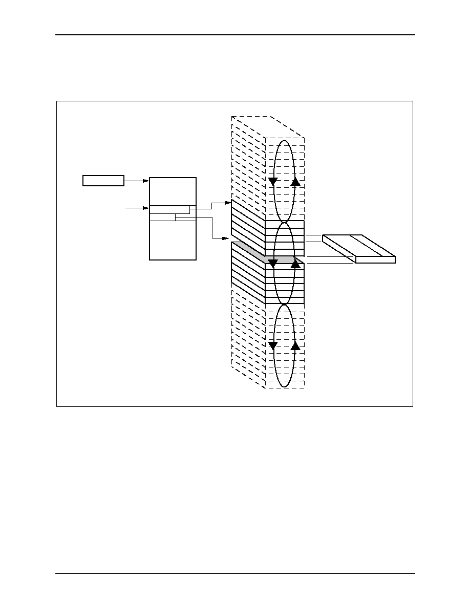
RS8234
5.0 Reassembly Coprocessor
ATM ServiceSAR Plus with xBR Traffic Management
5.6 Status Queue Operation
28234-DSH-001-B
Mindspeed Technologies
TM
5-33
Figure 5-15
illustrates this structure.
5.6.1.1 Setup
At system initialization, set up the following fields in each of the status queue
base table entries:
�
Write the base address of the corresponding status queue in the
BASE_PNTR field.
�
Initialize the WRITE and READ_UD fields to zeroes.
�
Set the SIZE field for the size of the corresponding status queue.
�
Set the LOCAL bit to a status high if the status queue is in local memory;
otherwise set the bit to a logic low.
In addition, initialize each status queue entry in all 32 status queues by setting
the VLD bit to a logic low.
Initialize the READ pointers to zero for each status queue.
Figure 5-15. Status Queue Structure Format
STAT
(From RSM VCC
Table Entry)
Status Queue Base Table
(Internal SRAM)
(32 entries in
the base table)
WRITE
(32 Status Queues)
BASE_PNTR
0x1000
BD
_PN
TR
100074_036

5.0 Reassembly Coprocessor
RS8234
5.6 Status Queue Operation
ATM ServiceSAR Plus with xBR Traffic Management
5-34
Mindspeed Technologies
TM
28234-DSH-001-B
5.6.1.2 Operation
The reassembly coprocessor normally writes a status queue entry when a
complete CPCS-PDU has been reassembled. It also writes a status queue entry for
each received OAM cell.
Each time the RSM coprocessor writes a status queue entry, it sets the VLD
bit in the entry to a logic high, and increments the WRITE pointer in the status
queue base table entry for that status queue.
When the host processes the status queue, it reads entries based on the host
READ pointer for that status queue. It reads only the VLD bit at first before
reading any other word, in order to maintain data coherency.
When the host finds the VLD bit set to a logic high, it processes the status
queue entry, increment the host READ counter and reset the VLD bit to a logic
low. The host also periodically writes the READ counter value to the READ_UD
field in the status queue base table entry for that queue.
When in Message Mode, the RSM coprocessor writes a status entry at the
completion of a CPCS-PDU. Optionally, a status entry can be written at both the
beginning and end of a message, to allow the host to initiate protocol header
processing in advance of receiving the complete message. The host can then
traverse the linked cell buffers to collect the complete CPCS-PDU.
If the BINTR bit in the RSM VCC Table entry is a logic high, the RSM
coprocessor writes an additional status queue entry at the completion of the first
buffer of a CPCS-PDU. This status queue entry is delineated by the BOM bit set
and the EOM bit cleared. This allows the host to begin packet processing before
reception of the complete CPCS-PDU. In this case only the BD_PNTR and
VCC_INDEX fields are valid in that status queue entry.
The STM_MODE bit in the RSM VCC Table, being set to a logic high,
activates Streaming Mode for that channel. In this mode, the RSM coprocessor
writes a status entry for each completed buffer. The BD_PNTR field in the status
entry points to the corresponding buffer descriptor for that single buffer. Only the
last status entry for that CPCS-PDU, with EOM bit a logic high, contains valid
status data for that PDU.
Refer to
Chapter 2.0
for more detailed information on the operation of status
queues.
5.6.1.3 Errors
The RSM coprocessor also writes a status entry for several error conditions,
including:
�
Reassembly time-out
�
Early packet discard
�
Per-channel firewall
�
CPCS abort
To ensure that an error indication occurs even if no CPCS-PDUs are being
reassembled on channels having free buffer queues in the empty state, a BOM cell
will cause a status queue entry to be written. If a BOM cell is received and no
early packet discards have occurred on channels mapped to the empty free buffer
queue, then a status queue entry is written with the BOM and UNDF bits set to a
logic high, and either the RSM_HF_EMPT bit in the HOST_ISTAT1 register or
the RSM_LF_EMPT bit in the LP_ISTAT1 register is set to a logic high. This
status does not point to a linked list of buffer descriptors. It will be written a
maximum of once per free buffer queue empty condition.

RS8234
5.0 Reassembly Coprocessor
ATM ServiceSAR Plus with xBR Traffic Management
5.6 Status Queue Operation
28234-DSH-001-B
Mindspeed Technologies
TM
5-35
5.6.1.4 Host Detection
of Status Queue Entries
The host can use either a polling operation or an interrupt routine to detect new
status queue entries.
To poll each status queue, the host continuously reads the VLD bit at the
current READ position until it returns a logic high. The host then processes the
status entry, writes the VLD bit to a logic low and increments its current READ
pointer. Periodically, the host writes the current READ index value into the
READ_UD field of the status queue base table entry.
The host can also use an interrupt routine to process status queues. When the
reassembly coprocessor writes a status queue entry into host memory, the
HOST_ISTAT0 (RSM_HS_WRITE) bit is set to a logic high to prompt an
interrupt. Upon receiving an interrupt, the host reads HOST_ST_WR
(RSM_HS_WRITE[15:0]) to determine which host memory status queue(s)
caused the interrupt.
NOTE:
Note that only status queues 0�15 are reported in this register.
A typical operation for the interrupt manager would be to only read
HOST_ISTAT1 upon receiving an interrupt, and periodically read
HOST_ISTAT0 to insure that no error conditions have occurred. Once the
interrupt manager has determined which status queue(s) caused the interrupt, the
host would start reading the appropriate status queues at their current read
location. The host processes status entries until reading an entry with the VLD bit
set to logic low. Again, the host periodically writes the current READ index value
into the READ_UD field of the status queue base table entry.
5.6.2 Status Queue Overflow or Full Condition
A status queue overflow or full condition is entered when the last available status
queue entry is written. The reassembly coprocessor detects the condition by
comparing the WRITE+1 and READ_UD index pointers. If the pointers are
equal, a status overflow condition is detected and the RSM coprocessor sets the
internal OVFL bit in the last status queue entry written to a logic high, to indicate
the condition. The RSM coprocessor also sets to one either the RSM_HS_FULL
bit in the HOST_ISTAT1 register, or the RSM_LS_FULL bit in the LP_ISTAT1
register, to prompt an interrupt.
While the reassembly coprocessor is in status full condition, it discards all
cells. If a COM or EOM cell is received while the status queue is full, the channel
is marked for status full packet discard. When an SSM, EOM, or OAM cell is
received during a status full condition, the cell is discarded and the status queue
checked. If there is now room in the status queue, then the status full condition is
exited.
For multiple peer configurations, an interrupt manager can be configured by
the user to detect the full condition and advise the peers to check if their queues
have overflowed. Each peer would then check the OVFL bit in the last status
queue entry written (pointed to by READ_UD � 1), to determine if that peer's
status queue has filled. If the OVFL bit is not set to a logic high, the host should
also check the entry pointed to by (READ_UD � 2) to determine if an overflow
condition occurred during a host update of the READ_UD index pointer. Since
the reassembly coprocessor recovers from the overflow condition automatically,
the host does not have to determine which queue overflowed.

5.0 Reassembly Coprocessor
RS8234
5.7 Reassembly Control and Status Structures
ATM ServiceSAR Plus with xBR Traffic Management
5-36
Mindspeed Technologies
TM
28234-DSH-001-B
After a status group has exited a full condition, the RSM coprocessor
performs EPD on channels marked for packet discard due to the status overflow
condition when a cell is received on any of those channels. Cells up to and
including the next EOM will also be discarded. Status queue overflow protection
can be globally disabled by setting RSM_CTRL0(RSM_STAT_DIS) to a logic
high.
NOTE:
Avoid having the Status Queue Overflow (or Full Condition) and DMA
FIFO Buffer Full conditions at the same time.
5.7 Reassembly Control and Status Structures
5.7.1 Channel Lookup Structures
The reassembly coprocessor uses a VPI/VCI Table Index mechanism employing
direct index lookup in order to assign each arriving cell to a virtual channel, based
on its VPI/VCI value.
Figure 5-16
illustrates this lookup mechanism.
Table 5-3
describes the normal VPI Index Table format (one word per entry)
without EN_PROG_BLK_SZ (RSM_CTRL1) enabled.
Table 5-4
describes the VPI Index Table format (two words per entry) with
programmable VCC Table and VCI Index Table block size enabled.
Table 5-5
describes the field definitions for the VPI Index Table fields.
Figure 5-16. VPI/VCI Channel Lookup Structure
Base Register (16)
VPI Index Table
VCI Index Table
(For One VPI)
RSM_TBASE
(RSM_ITB)
VPI [11:0]
VCI [15:x]
VCI_IT_PNTR
VCC_BLOCK_INDEX
(Either 256 or 4096 entries)
Where x=6; or value of VCI_IT_BLK_SZ
with EN_PROG_BLK_SZ enabled
100074_037
Table 5-3. Normal VPI Index Table Entry Format
Word
31 30 29 28 27 26 25 24 23 22 21 20 19 18 17 16 15 14 13 12 11 10 9 8 7 6 5 4 3 2 1 0
0
VP
_E
N
VCI_RANGE
VCI_IT_PNTR
RS8234
5.0 Reassembly Coprocessor
ATM ServiceSAR Plus with xBR Traffic Management
5.7 Reassembly Control and Status Structures
28234-DSH-001-B
Mindspeed Technologies
TM
5-37
Table 5-6
describes the VCI Index Table format without the programmable VCC
Table and VCI Index Table block size enabled.
Table 5-7
describes the VCI Index Table format with EN_PROG_BLK_SZ
(RSM_CTRL1) enabled.
Table 5-8
describes the VCI Index Table Descriptions.
Table 5-4. VPI Index Table Entry Format with EN_PROG_BLK_SX(RSM_CTRL1) Enabled
Word
31 30 29 28 27 26 25 24 23 22 21 20 19 18 17 16 15 14 13 12 11 10 9 8 7 6 5 4 3 2 1 0
0
VP
_E
N
Reserved
VCI_IT_PNTR
1
Reserved
VCI_RANGE
Table 5-5. VPI Index Table Entry Descriptions
Field Name
Description/Function
VP_EN
Enables the VPI for lookup processing. If not enabled, cell is discarded, and the CELL_DSC_CNT
counter is incremented.
VCI_RANGE
Determines the maximum VCI value allowed. If cell VCI exceeds maximum, cell is discarded, and
counted as CELL_DSC_CNT.
In normal operation, the 10 Most Significant Bits can be set by the user, with the 6 Least
Significant Bits set at 1. When EN_PROG_BLK_SZ(RSM_CTRL1) is enabled, all 16 baits of the field
can be set by the user.
VCI_IT_PNTR
VCI Index Table Base Pointer. Points to the base of the VCI Index Table for the VPI by appending two
least significant zero bits to form a byte address.
Table 5-6. Normal VCI Index Table Format
Word 31 30 29 28 27 26 25 24 23 22 21 20 19 18 17 16 15 14 13 12 11 10 9
8
7
6
5
4
3
2
1
0
0
Reserved
VCC_BLOCK_INDEX
Reserved
Table 5-7. VCI Index Table Format with EN_PROG_BLK_SZ(RSM_CTRL1) Enabled
Word 31 30 29 28 27 26 25 24 23 22 21 20 19 18 17 16 15 14 13 12 11 10 9
8
7
6
5
4
3
2
1
0
0
BL
K_
EN
Reserved
VCC_BLOCK_INDEX
Table 5-8. VCI Index Table Descriptions
Field Name
Description/Function
BLK_EN
Block Enable. If logic high, enables entry. If a logic low, the cell is discarded.
5.0 Reassembly Coprocessor
RS8234
5.7 Reassembly Control and Status Structures
ATM ServiceSAR Plus with xBR Traffic Management
5-38
Mindspeed Technologies
TM
28234-DSH-001-B
5.7.2 Reassembly VCC Table
Each reassembly VCC Table entry occupies one 12-word descriptor of the
reassembly VCC Table.
There are three basic formats for the reassembly VCC Table entry -- AAL5,
AAL0, and AAL3/4. Each completely describe the state of the reassembly
process for individual VCCs. In addition, the AAL3/4 Head VCC Table entry
describes the AAL3/4-specific reassembly process state for an AAL3/4 VCC.
Figure 5-17
illustrates the VCC Table entry lookup mechanism as a
continuation from
Figure 5-16
.
VCC_BLOCK_INDEX
VCC block index.
When EN_PROG_BLK_SZ is not enabled, this is the index to the block of 64 RSM VCC Table entries
allocated to VCI[15:6]. In this case, VCC_BLOCK_INDEX is concatenated with the six least significant
bits of the VCI to form the index into the RSM VCC Table to access the VCC Table entry for that channel.
When EN_PROG_BLK_SZ is enabled, the [16 - (value of VCI_IT_BLK_SZ)] most significant bits of
VCC_BLK_INDEX are concatenated with the [(value of VCI_IT_BLK_SZ) - 1] least significant bits of the
VCI to form the index into the VCC Table to access the VCC Table entry. For example, if the value of
VCI_IT_BLK_SZ = 4, then the resultant RSM VCC_INDEX pointer = {VCC_BLK_INDEX[15:4],
CELL_VCI[3:0]}.
Table 5-8. VCI Index Table Descriptions
Field Name
Description/Function
Figure 5-17. Reassembly VCC Table Entry Lookup Mechanism
Base Register
RSM_TBASE(RSM_VCCB)
VCC_BLOCK_INDEX
VCI[5:0]
100074_038
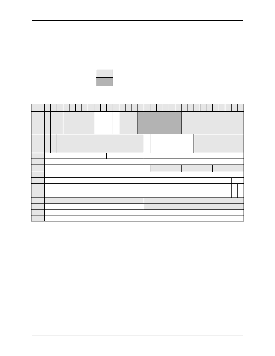
RS8234
5.0 Reassembly Coprocessor
ATM ServiceSAR Plus with xBR Traffic Management
5.7 Reassembly Control and Status Structures
28234-DSH-001-B
Mindspeed Technologies
TM
5-39
5.7.2.1 AAL5, AAL0,
and AAL3/4 VCC Table
Entries
Table 5-9
describes the format of AAL5 reassembly VCC Table entries.
Table 5-10
describes the format of AAL0 RSM VCC Table entries.
Table 5-11
describes the format of AAL3/4 RSM VCC Table entries.
KEY:
= Written by host at VCC setup.
= May be dynamically modified during active reassembly.
Table 5-9. Reassembly VCC Table Entry Format - AAL5
Word 31 30 29 28 27 26 25 24 23 22 21 20 19 18 17 16 15 14 13 12 11 10 9
8
7
6
5
4
3
2
1
0
0
VC
_
E
N
AAL
_TYPE
DPRI
Reserved
FF
_
D
S
C
T
O
_
I
NDEX
PM_INDEX
AAL_EN
1
T
O
_L
AST
TO
_
E
N
CUR_TOCNT
ER_E
FCI
Reserved
ABR_CTRL
2
PDU_FLAGS
Reserved
TOT_PDU_LEN
3
CRCREM
4
CBUFF_LEN
FW
STAT
BFR1
BFR0
5
CBUFF_PNTR
6
BOM_BD_PNTR
Rsvd
7
CURR_BD_PNTR
Rsv
d
CBFR1
8
SEG_VCC_INDEX
SERV_DIS
9
Reserved
RX_COUNTER/VPC_INDEX
10
Reserved
11
Reserved
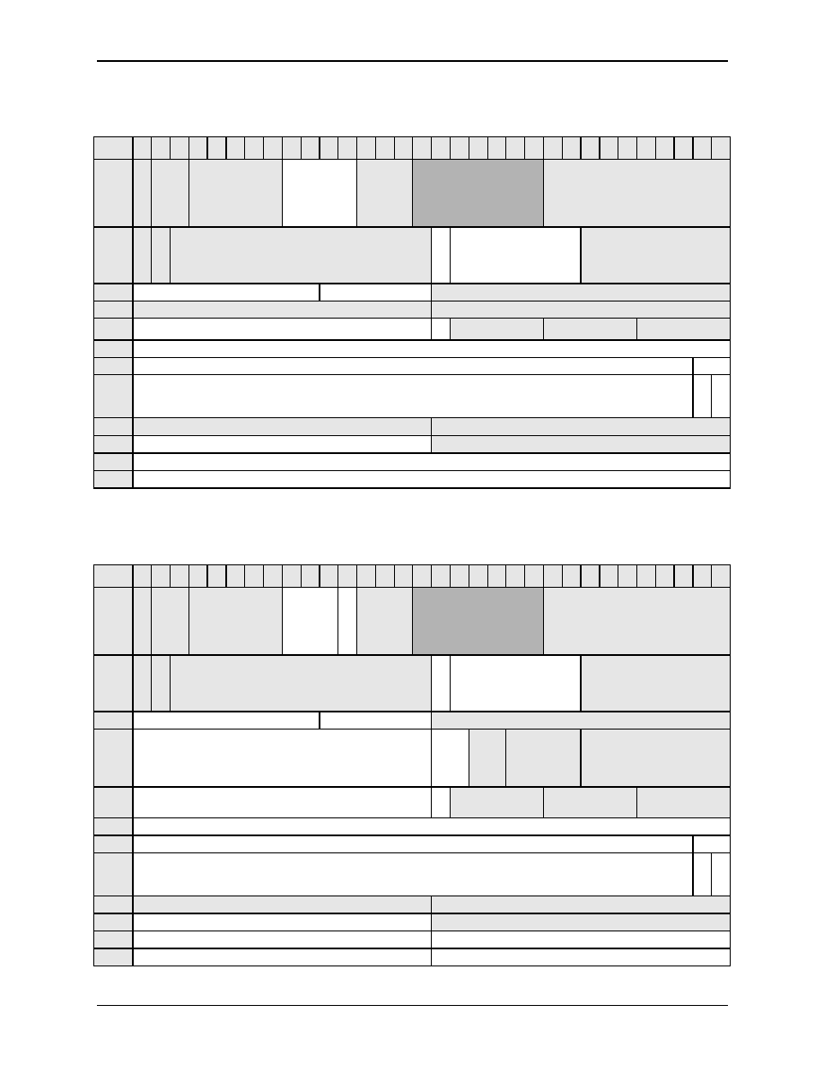
5.0 Reassembly Coprocessor
RS8234
5.7 Reassembly Control and Status Structures
ATM ServiceSAR Plus with xBR Traffic Management
5-40
Mindspeed Technologies
TM
28234-DSH-001-B
See the following tables for the AAL3/4 Head VCC structure and field
definitions.
Table 5-10. Reassembly VCC Table Entry Format - AAL0
Word 31 30 29 28 27 26 25 24 23 22 21 20 19 18 17 16 15 14 13 12 11 10 9
8
7
6
5
4
3
2
1
0
0
VC_
E
N
AAL_
T
YPE
DPRI
Reserved
T
O
_
I
NDEX
PM_INDEX
AAL_EN
1
T
O
_L
AST
TO
_
E
N
CUR_TOCNT
ER_EF
C
I
Reserved
ABR_CTRL
2
PDU_FLAGS
Reserved
TOT_PDU_LEN
3
CCOUNT
TCOUNT
4
CBUFF_LEN
FW
STAT
BFR1
BFR0
5
CBUFF_PNTR
6
BOM_BD_PNTR
Rsvd
7
CURR_BD_PNTR
Rsv
d
CBFR1
8
SEG_VCC_INDEX
SERV_DIS
9
Reserved
RX_COUNTER/VPC_INDEX
10
Reserved
11
Reserved
Table 5-11. Reassembly VCC Table Entry Format - AAL3/4
Word 31 30 29 28 27 26 25 24 23 22 21 20 19 18 17 16 15 14 13 12 11 10 9
8
7
6
5
4
3
2
1
0
0
VC_
E
N
AAL_
T
YPE
DPRI
Reserved
FF
_DSC
T
O
_
I
NDEX
PM_INDEX
AAL_EN
1
T
O
_L
AST
TO
_
E
N
CUR_TOCNT
ER_EF
C
I
Reserved
ABR_CTRL
2
PDU_FLAGS
Reserved
TOT_PDU_LEN
3
BASIZE
Rsvd
NEXT
_ST
NEXT_SN
BTAG
4
Reserved
Rs
vd
STAT
BFR1
BFR0
5
CBUFF_PNTR
6
BOM_BD_PNTR
Rsvd
7
CURR_BD_PNTR
Rs
vd
CBFR1
8
SEG_VCC_INDEX
SERV_DIS
9
Reserved
RX_COUNTER/VPC_INDEX
10
Reserved
Reserved
11
Reserved
Reserved

RS8234
5.0 Reassembly Coprocessor
ATM ServiceSAR Plus with xBR Traffic Management
5.7 Reassembly Control and Status Structures
28234-DSH-001-B
Mindspeed Technologies
TM
5-41
Table 5-12
illustrates the PDU_FLAGS field bit definitions.
Table 5-13
illustrates the ABR_CTRL field bit definitions.
Table 5-14
illustrates the
AAL_EN field bit definitions.
Table 5-12. PDU_FLAGS Field Bit Definitions
Bit
31
30
29
28
27
26
25
24
23
22
CNT_ROVR SFPD_PND
EPD
CI
CLP
BFR_LOCAL BD_LOCAL ACT_PDU
BOM_BUF FFPD_PND
Table 5-13. ABR_CTRL Field Bit Definitions
Bit
7
6
5
4
3
2
1
0
ER_EN
Reserved
Reserved
ABR_VPC
Reserved
Reserved
Reserved
Reserved
Table 5-14. AAL_EN Field Bit Definitions
Bit
9
8
7
6
5
4
3
2
1
0
PM_EN
FIFO_EN
LNK_EN
FW_EN
M52_EN
BINTR
STM_MODE LECID_EN
FRD_EN
CLPD_EN

5.0 Reassembly Coprocessor
RS8234
5.7 Reassembly Control and Status Structures
ATM ServiceSAR Plus with xBR Traffic Management
5-42
Mindspeed Technologies
TM
28234-DSH-001-B
Table 5-15
details the descriptions of the reassembly VCC Table fields.
Table 5-15. Reassembly VCC Table Descriptions (1 of 3)
Field Name
Description/Function
VC_EN
Enables the VCC Table entry. If disabled, the cell is discarded.
AAL_TYPE
When VC_EN is a logic high, configure channel to process specific AA; otherwise, when VC_EN is a
logic low, a value of "11" will cause the CELL_DSC_CNT counter not to be incremented.
00 - AAL5
01 - AAL0
10 - AAL3/4
11 - Reserved
DPRI
Discard Priority value. Compared against global priority in CLP and Frame Relay discard modes to
determine discard eligibility. In LANE-LECID echo suppression mode, this field is the index into the
LECID table that holds channel LECID values.
FF_DSC
FIFO Full Discard. When a logic high, cells will be discarded when incoming DMA FIFO is almost
full. This includes OAM cells when RSM_CTRL1(OAM_QU_EN) is a logic low.
TO_INDEX
Selects one of eight INIT_TOCNT values in internal SRAM.
PM_INDEX
Pointer to a PM OAM processing word. Index with reference to top of VPI Index table.
AAL_EN
Enable various cell processes. The AAL_EN field contains the following control bits:
PM_EN--Enable PM OAM processing on this channel.
FIFO_EN--Enable Logical FIFO mode.
LNK_EN--Enable writing of buffer descriptor NEXT field.
FW_EN--Enable firewall processing. Used in conjunction with FWALL_EN bit in RSM_CTR0.
M52_EN--f set high, all 52 octets of the cell are written to a cell buffer.
BINTR--Enable interrupt after BOM buffer filled in Message Mode.
STM_MODE--Enable Streaming Mode.
LECID_EN--Enable LANE-LECID echo suppression. Invalid in AAL3/4.
FRD_EN--Enable frame relay DE (Discard Eligibility) mode. Invalid in AAL3/4.
CLPD_EN--Enable CLP discard mode. Invalid in AAL3/4.
LNK_EN
FW_EN
M52_EN
BINTR
STM_MODE
LECID_EN
FRD_EN CLPD_EN
FIFO_EN
PM_EN
9
8
7
6
5
4
3
2
1
0
RS8234
5.0 Reassembly Coprocessor
ATM ServiceSAR Plus with xBR Traffic Management
5.7 Reassembly Control and Status Structures
28234-DSH-001-B
Mindspeed Technologies
TM
5-43
PDU_FLAGS
Set various flags related to PDUs. The PDU_FLAGS field contains the following control bits:
CNT_ROVR--Indication that SERVICE_CNT counters have rolled over. The next status entry will
indicate this condition.
SFPD_PND--Status Full Packet Discard Pending. Set when status queue is full, and CPCS needs to
be discarded when status entries available.
EPD--EPD Flag. Set when early packet discard occurs on a channel. Cleared when new packet
starts and error condition cleared.
CI --Congestion Indication. PTI[1] header bit ORed across the CPCS-PDU.
CLP--Cell Loss Priority. CLP header bit ORed across the CPCS-PDU.
BFR_LOCAL--Buffer Local. If high, the current cell buffer is located in local memory; otherwise,
host memory. SAR maintains this bit.
BD_LOCAL--Buffer Descriptor Local. If high, the buffer descriptors reside in local memory;
otherwise, host memory. SAR maintains this bit.
ACT_PDU--Active PDU. Indication that at least one buffer has been taken off of the free buffer
queue for the current PDU being received.
BOM_BUF--BOM buffer flag. Set high when filling the first buffer of a PDU.
FFPD_PND--DMA FIFO Full Packet Discard Pending.
ER_EFCI
ER EFCI bit of the previous data cell.
ABR_CTRL
Set various control bits related to QFC. The QFC_CTRL field contains the following control bits:
ER_EN--Enable ER operation.
ABR_VPC--Indicates ER connection is VPC (zero indicates VCC). For VPC operation, all VCC
entries in the VPC group except VCI=6, must be initialized with VPC_INDEX pointing to the VCC
entry corresponding with VCI=6. The VCI=6 entry contains the integrated EFCI bit over the VPC
group. Also, all entries in the VPC group including VCI=6 must set the ABR_VPC bit to a logic high.
TOT_PDU_LEN
Total PDU length in bytes.
TO_LAST
Indicates the last VCC table entry to process for time-out.
TO_EN
Enable time-out processing on the channel.
CUR_TOCNT
Current time-out counter for the channel.
CRCREM
Cycle Redundancy Check Remainder. CRC32 remainder used in AAL5 only.
CCOUNT
Termination Cell count. Used in AAL0 to terminate packet. When PTI termination mode is enabled,
the maximum total length of a CPCS-PDU is CCOUNT * 2 bytes. In fixed length mode, initialize to
one.
TCOUNT
Termination Count. Used in AAL0 to determine the number of cells in a packet. If this field is zero in
AAL0 mode, then PTI termination mode is enabled.
CBUFF_LEN
Current bufferlength. Unused space of the current buffer in bytes.
FW
Firewall condition. Indicates that a firewall condition has occurred.
Table 5-15. Reassembly VCC Table Descriptions (2 of 3)
Field Name
Description/Function
CNT_ROVR
SFPD_PND
EPD
CI
CLP
BFR_LOCAL
BD_LOCAL
BOM_BUF
ACT_PDU
FFPD_PND
31
30
29
28
27
26
24
25
23
22
ER_EN
Reserved
ABR_VPC
Reserved
Reserved
Reserved
Reserved
6
5
4
2
1
0
3

5.0 Reassembly Coprocessor
RS8234
5.7 Reassembly Control and Status Structures
ATM ServiceSAR Plus with xBR Traffic Management
5-44
Mindspeed Technologies
TM
28234-DSH-001-B
BASIZE
AAL3/4 BASize field. Used to record the BASize field from the AAL3/4 PDU, in order to check
against the LENGTH field in the AAL3/4 PDU trailer.
NEXT_ST
Next Segment Type (ST) expected.
NEXT_SN
Next Sequence Number (SN) expected.
BTAG
Records the AAL3/4 CPCS-PDU's Btag field, in order to check against the Etag field in the
CPCS-PDU trailer.
STAT
Status queue pool number.
BFR1
COM free buffer queue pool number.
BFR0
BOM free buffer queue pool number.
CBUFF_PNTR
Current buffer pointer. Pointer to the current unused position of the cell buffer where cell payload
data may be written. In Logical FIFO Mode, the address of the FIFO.
BOM_BD_PNTR
BOM buffer descriptor pointer. Pointer to the BOM buffer descriptor.
CBFR1
Current BFR1 indication. A logic high indicates that current buffer is from BFR1 pool and logic low
indicates from BFR0 pool.
CURR_BD_PNTR
Current buffer descriptor pointer. Pointer to the buffer descriptor corresponding to the current
buffer in use.
SEG_VCC_INDEX
Channel index of corresponding segmentation channel. Used by ER and PM-OAM processing.
SERV_DIS
Service Discard counter. Counts the number of CPCS-PDUs discarded due to either LANE_LECID
echo suppression, CLP discard, or frame relay DE discard.
RX_COUNTER/
VPC_INDEX
When ABR_VPC is a logic low, RX_COUNTER is the firewall mode credit counter. When ABR_VPC is
a logic high, VPC_INDEX is used to control a VPC group. See ABR_VPC for description of this field.
Table 5-15. Reassembly VCC Table Descriptions (3 of 3)
Field Name
Description/Function
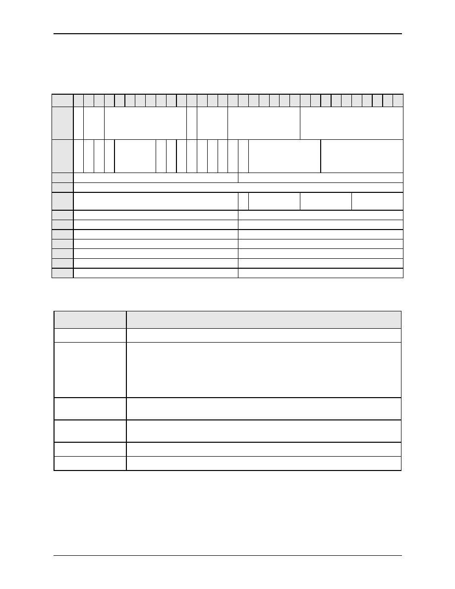
RS8234
5.0 Reassembly Coprocessor
ATM ServiceSAR Plus with xBR Traffic Management
5.7 Reassembly Control and Status Structures
28234-DSH-001-B
Mindspeed Technologies
TM
5-45
5.7.2.2 AAL3/4 Head
VCC Table Entry
Table 5-16
shows the AAL3/4 Head VCC Table structure.
Table 5-17
details the
AAL3/4 Head VCC Table field definitions.
Table 5-16. AAL3/4 Head VCC Table Entry Format
Word 31 30 29 28 27 26 25 24 23 22 21 20 19 18 17 16 15 14 13 12 11 10 9
8
7
6
5
4
3
2
1
0
0
V
C
_EN
AA
L_
TY
PE
Reserved
FF_
D
S
C
Rsvd
PM_INDEX
AAL_EN
1
TO
_
L
A
S
T
TO_
E
N
Rs
v
d
MI
D
0
MID_BITS
CR
C10
_
E
N
LI
_
E
N
S
T
_EN
SN_
E
N
CP
I_E
N
BA
T_
EN
BA
H
_EN
Rs
v
d
ER_
E
F
C
I
Reserved
ABR_CTRL
2
Reserved
VCC_INDEX_BASE
3
Reserved
4
Reserved
Rs
v
d
STAT
BFR1
BFR0
5
CRC10_ERR
MID_ERR
6
LI_ERR
SN_ERR
7
BOM_SSM_ERR
EOM_ERR
8
SEG_VCC_INDEX
Reserved
9
Reserved
RX_COUNTER/VPC_INDEX
10
Reserved
Reserved
11
Reserved
Reserved
Table 5-17. AAL3/4 Head VCC Table Descriptions (1 of 3)
Field Name
Description/Function
VC_EN
Enables the VCC table entry. If disabled, the cell is discarded.
AAL_TYPE
When VC_EN is a logic high, configure channel to process specific AAL; otherwise, when VC_EN is a
logic low, a value of "11" will cause the CELL_DSC_CNT counter not to be incremented.
00 - AAL5
01 - AAL0
10 - AAL3/4
11 - Reserved
FF_DSC
FIFO Full Discard. When a logic high and RSM_CTRL1(OAM_QU_EN) is a logic low, OAM cells will
be discarded when the incoming DMA FIFO is almost full.
PM_INDEX
Pointer to a PM-OAM processing word. Index with reference to top of VPI Index Table. Used by the
OAM cells detected on AAL3/4 channels.
AAL_EN
Same as AAL_EN field in standard RSM VCC entry. Used by OAM cells detected on AAL3/4 channels.
MID0
When logic high, allow a MID value of zero; otherwise, zero is invalid.

5.0 Reassembly Coprocessor
RS8234
5.7 Reassembly Control and Status Structures
ATM ServiceSAR Plus with xBR Traffic Management
5-46
Mindspeed Technologies
TM
28234-DSH-001-B
MID_BITS
Number of significant bits for MID field. Defines the limit of MID values allowed for the AAL3/4
Virtual Connection. If the MID_BITS subfield is nonzero and the AAL_TYPE is AAL3/4, CPCS_MID
multiplexing processing is enabled. A MID of zero is valid only if MID0 is a logic high. MID_BITS is
decoded as follows:
CRC10_EN
If set high, enable AAL3/4 CRC 10 field checking and error counting.
LI_EN
If set high, enable AAL3/4 LI field checking and error counting.
ST_EN
If set high, enable AAL3/4 ST field checking and error counting.
SN_EN
If set high, enable AAL3/4 SN field checking and error counting.
CPI_EN
If set high, enable AAL3/4 CPI field checking.
BAT_EN
If set high, enable AAL3/4 BASIZE
Length checking. If low, LENGTH > BASIZE check is performed.
BAH_EN
If set high, enable AAL3/4 BASIZE < 37 checking.
VCC_INDEX_BASE
Pointer to the first VCC table entry for this VCC with MID value = zero. All multiplexed MIDs on this
channel are contained in a contiguous block of VCC table entries.
TO_LAST
Indicates the last entry in the VCC Table in which time-out processing occurs.
Table 5-17. AAL3/4 Head VCC Table Descriptions (2 of 3)
Field Name
Description/Function
MID_BITS
Range of MID values
0000
MID processing disabled
0001
0 / 1-1
0010
0 / 1-3
0011
0 / 1-7
0100
0 / 1-15
0101
0 / 1-31
0110
0 / 1-63
0111
0 / 1-127
1000
0 / 1-255
1001
0 / 1-511
1010
0 / 1-1023
1011
Reserved
1100
Reserved
1101
Reserved
1110
Reserved
1111
Reserved
RS8234
5.0 Reassembly Coprocessor
ATM ServiceSAR Plus with xBR Traffic Management
5.7 Reassembly Control and Status Structures
28234-DSH-001-B
Mindspeed Technologies
TM
5-47
5.7.3 Reassembly Buffer Descriptor Structure
Reassembly buffer descriptors reside on word-aligned addresses in host memory.
The host controls the allocation and management of reassembly buffer
descriptors.
During initialization, in each buffer descriptor entry, the host writes a pointer
to an associated reassembly data buffer, in the BUFF_PTR field.
Table 5-18
and
Table 5-19
describe the format of the reassembly buffer
descriptors.
TO_EN
Enable time-out process of the VCC entry. Must be set to a logic zero.
CRC10_ERR
Number of AAL3/4 cells received with CRC10 error.
MID_ERR
Number of AAL3/4 cells received that did not have an active MID as determined by the MID_BITS
and MID0 fields.
LI_ERR
Number of AAL3/4 cells received that had an unexpected LI value.
SN_ERR
Number of AAL3/4 cells received that had an unexpected SN value.
BOM_SSM_ERR
Number of unexpected AAL3/4 BOM or SSM cells received.
EOM_ERR
Number of unexpected AAL3/4 EOM cells received.
Table 5-17. AAL3/4 Head VCC Table Descriptions (3 of 3)
Field Name
Description/Function
Table 5-18. Reassembly Buffer Descriptor Structure
Word 31 30 29 28 27 26 25 24 23 22 21 20 19 18 17 16 15 14 13 12 11 10 9
8
7
6
5
4
3
2
1
0
0
NEXT_PTR
1
BUFF_PTR
Table 5-19. Reassembly Buffer Descriptor Structure Definitions
Field Name
Description/Function
NEXT_PTR
Pointer to the address of the next buffer descriptor.
BUFF_PTR
Pointer to the address of the data cell buffer.
NOTE:
The SAR does not access this word; the user may place it anywhere in the buffer
descriptor.
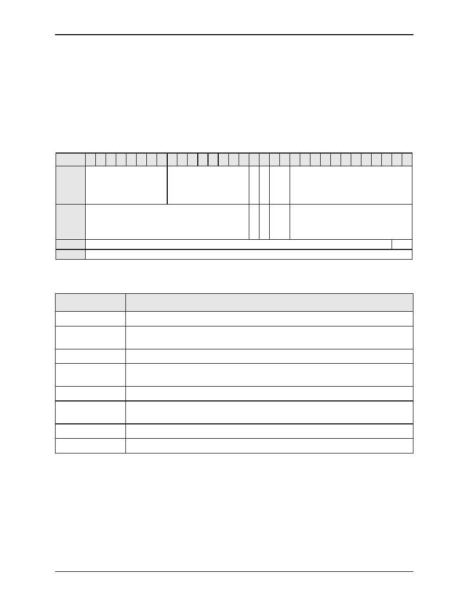
5.0 Reassembly Coprocessor
RS8234
5.7 Reassembly Control and Status Structures
ATM ServiceSAR Plus with xBR Traffic Management
5-48
Mindspeed Technologies
TM
28234-DSH-001-B
5.7.4 Free Buffer Queues
The host initializes the free buffer queues in SAR shared memory, and during
reassembly processing submits data buffers for reassembly to the free buffer
queues.
The free buffer queue base table is located in RS8234 internal memory.
Table 5-20
and
Table 5-21
describe the format of the free buffer queue base table
entries.
Table 5-20. Free Buffer Queue Base Table Entry Format
Word
31 30 29 28 27 26 25 24 23 22 21 20 19 18 17 16 15 14 13 12 11 10 9
8 7 6
5 4 3
2 1 0
0
Reserved
UPDATE
EM
P
T
BF
R_
LO
C
A
L
Rsvd
READ
1
LENGTH
R
svd
BD_
L
O
CAL
Rsvd
FORWARD
2
READ_UD_PNTR
Rsvd
3
Reserved
Table 5-21. Free Buffer Queue Base Table Entry Descriptions
Field Name
Description/Function
UPDATE
Read Index Pointer Update Interval counter.
EMPT
Free buffer queue Empty flag. Used to indicate that an appropriate status entry has been written to
indicate the empty condition.
BFR_LOCAL
If logic high, cell buffers located in SAR shared memory, otherwise in host memory.
BD_LOCAL
If logic high, buffer descriptor and READ_UD word are located in SAR shared memory, otherwise in
host memory.
READ
Current READ index pointer.
LENGTH
Length in bytes of buffers in queue. Even though LENGTH is in bytes, the user must set the length to a
mod-32 bit boundary.
FORWARD
Current Forward Processing Read index pointer (firewalling).
READ_UD_PNTR
Word address in user memory to write READ pointer every UPDATE interval.

RS8234
5.0 Reassembly Coprocessor
ATM ServiceSAR Plus with xBR Traffic Management
5.7 Reassembly Control and Status Structures
28234-DSH-001-B
Mindspeed Technologies
TM
5-49
Table 5-22
and
Table 5-23
describe the format of the free buffer queue entries.
Table 5-22. Free Buffer Queue Entry Format
Word
31 30 29 28 27 26 25 24 23 22 21 20 19 18 17 16 15 14 13 12 11 10 9
8 7 6
5 4 3
2 1 0
0
BUFFER_PNTR
1
BD_PNTR
Rs
v
d
VL
D
2
(1)
Reserved
Rs
v
d
FW
D
_
V
L
D
VCC_INDEX
3
(1)
(not used)
NOTE(S):
(1)
These words are used only in Bank 0 if RSM_FBQCTL(FBQ0_RTN) = 1.
Table 5-23. Free Buffer Queue Entry Descriptions
Field Name
Description/Function
BUFFER_PNTR
Pointer to beginning of cell buffer.
BD_PNTR
Pointer to corresponding cell buffer descriptor.
VLD
Free buffer Valid Bit. If high, location has a valid free buffer.
Rsvd
Always set to zero.
FWD_VLD
Forward Valid. If logic high, word contains valid buffer return information.
VCC_INDEX
Channel of corresponding buffer return.

5.0 Reassembly Coprocessor
RS8234
5.7 Reassembly Control and Status Structures
ATM ServiceSAR Plus with xBR Traffic Management
5-50
Mindspeed Technologies
TM
28234-DSH-001-B
5.7.5 Reassembly Status Queues
The RS8234 reports reassembly status to the host on any one of 32 reassembly
status queues.
At initialization the host assigns the location and size of up to 32 RSM status
queues by initializing the reassembly status queue base table entries in RS8234
internal memory. The location and size of each RSM status queue is
independently programmable via these base table entries.
Table 5-24
and
Table 5-25
describe the format of the reassembly status queue
base table entries.
Table 5-26
through
Table 5-33
describe the formats of the reassembly status
queue entries.
Table 5-24. Reassembly Status Queue Base Table Entry Format
Word
31 30 29 28 27 26 25 24 23 22 21 20 19 18 17 16 15 14 13 12 11 10 9
8 7 6
5 4 3
2 1 0
0
BASE_PNTR
Rs
v
d
LO
CAL
1
SIZE
Rsvd
WRITE
Rsvd
READ_UD
Table 5-25. Reassembly Status Queue Base Table Entry Descriptions
Field Name
Description/Function
BASE_PNTR
Base pointer. Pointer to the base word address of the status queue.
LOCAL
If set high, queue is located in local memory, otherwise it is located in host memory.
SIZE
Size of the status queue.
00 = 64
01 = 256
10 = 1,024
11 = 4,096
WRITE
Current Write index pointer maintained by the SAR.
READ_UD
Periodic Read update index pointer maintained by the user.
Table 5-26. Reassembly Status Queue Entry Format with FWD_PM = 0
Word
31 30 29 28 27 26 25 24 23 22 21 20 19 18 17 16 15 14 13 12 11 10 9
8 7 6
5 4 3
2 1 0
0
BD_PNTR
"00"
1
UU
CPI
CPCS_LENGTH
2
Rsvd
PDU_CHECKS
VCC_INDEX
3
VLD
Reserved
Reserved
STATUS
FWD
_
P
M
OAM
STM

RS8234
5.0 Reassembly Coprocessor
ATM ServiceSAR Plus with xBR Traffic Management
5.7 Reassembly Control and Status Structures
28234-DSH-001-B
Mindspeed Technologies
TM
5-51
Table 5-27. Reassembly Status Queue Entry Format with FWD_PM = 1
Word
31 30 29 28 27 26 25 24 23 22 21 20 19 18 17 16 15 14 13 12 11 10 9
8 7 6
5 4 3
2 1 0
0
BD_PNTR
"00"
1
TRCC0
TRCC0+1
2
Rsvd
PDU_CHECKS
VCC_INDEX
3
VL
D
Reserved
BIPV
OV
F
L
CNT
_
R
O
VR
FWD
_
P
M
OAM
STM
Table 5-28. Reassembly Status Queue Entry Format with FWD_PM = 0 and AAL34 = 1
Word
31 30 29 28 27 26 25 24 23 22 21 20 19 18 17 16 15 14 13 12 11 10 9
8 7 6
5 4 3
2 1 0
0
BD_PNTR
"00"
1
HEAD_VCC_INDEX
CPCS_LENGTH
2
Rsvd
PDU_CHECKS
VCC_INDEX
3
VL
D
Reserved
AA
L3
4
Reserved
STATUS
FWD
_
P
M
OAM
STM
Table 5-29. PDU_CHECKS Field Bits
Bit
29
28
27
26
25
24
23
22
21
20
19
18
17
16
MO
D
_
E
R
R
O
R
B
A
_
E
R
ROR
A
L
_
E
R
ROR
L
E
N
_
E
RROR
P
A
D
_
E
RRO
R
CP
I_E
RRO
R
T
A
G_
E
RROR
C
R
C_
ER
ROR
S
T
_
E
R
ROR
SN_
E
RR
OR
L
I
_E
RRO
R
LP
CI_
L
AST
CI
Table 5-30. PDU_CHECKS Field Bits with CNT_ROVR = 1 and AAL34 = 1
Bit
29
28
27
26
25
24
23
22
21
20
19
18
17
16
M
O
D_E
RRO
R
B
A
_
E
RR
OR
A
L
_
E
R
ROR
L
E
N_
ER
ROR
P
A
D
_
E
RROR
CPI
_E
RROR
T
A
G_
ER
ROR
C
R
C_
ER
ROR
ST
_E
PD
SN_
E
P
D
LI
_
E
P
D
A3L2_ERR
Table 5-31. STATUS Field Bits
Bit
16
15
14
13
12
11
10
9
8
FFPD
EPD
FW
UNDF
OVFL
SFPD
TO
ABORT
CNT_ROVR
Table 5-32. STM Field Bits
Bit
3
2
1
0
EOM
BOM
STM_MODE
BFR1

5.0 Reassembly Coprocessor
RS8234
5.7 Reassembly Control and Status Structures
ATM ServiceSAR Plus with xBR Traffic Management
5-52
Mindspeed Technologies
TM
28234-DSH-001-B
Table 5-33. Reassembly Status Queue Entry Descriptions (1 of 2)
Field Name
Description/Function
BD_PNTR
Bufferdescriptor pointer. In Message Mode, pointer to the first buffer descriptor in the linked list. In
Streaming Mode, pointer to an individual buffer descriptor.
UU
AAL5 CPCS-UU field.
CPI
AAL5 CPCS-CPI field. In AAL0 PTI terminated mode, the least significant bit contains the most
significant bit of the total PDU length. The CPCS_LENGTH field contains the 16 least significant bits.
HEAD_VCC_INDEX
AAL3/4 Head VCC Table entry index. When CNT_ROVR = 1, AAL34 = 1, and FWD_PM = 0, this field
along with A3L2_ERR in the PDU_CHECKS field points to the MID that rolled over. This field is also
active when CNT_ROVR=0, AAL34=1, and FWD_PM=0.
CPCS_LENGTH
AAL5 CPCS-LENGTH field. In AAL0 PTI terminated mode, it is the 16 least significant bits of the total
PDU length. The CPI field contains the most significant bit.
PDU_CHECKS
Set various error flags related to PDUs.
MOD_ERROR--AAL3/4 CPCS-PDU is not 32-bit aligned.
BA_ERROR--AAL5: Indicates that the total PDU length exceeds maximum length when AUU = 1.
AAL3/4: BASIZE field error occurred.
AL_ERROR--AAL3/4 AL field is not all zeros.
LEN_ERROR--Total CPCS-PDU length exceeds maximum length and not at end of message.
PAD_ERROR--Pad field length is not correct.
CPI_ERROR--CPI field is not all zero.
TAG_ERROR--AAL3/4 Btag and Etag fields in the CPCS-PDU do not match.
CRC_ERROR--AAL5 CPCS or OAM CRC error.
ST_EPD--AAL3/4 Segment Type error; causes EPD.
SN_EPD--AAL3/4 Sequence Number error; causes EPD.
LI_EPD--AAL3/4 SAR-PDU length error; causes EPD.
LP--Value of CLP header bit ORed across the CPCS-PDU.
CI_LAST--Value of the PTI[1] header bit in the last cell of the CPCS-PDU.
CI--Value of the PTI[1] header bit ORed across the CPCS-PDU.
A3L2_ERR--When CNT_ROVR = 1, AAL34 = 1, and FWD_PM = 0, indicates which MIB counter rolled
over, based on these values:
0 = MID_ERR
1 = CRC10_ERR
2 = SN_ERR
3 = LI_ERR
4 = EOM_ERR
5 = BOM_SSM_ERR
VCC_INDEX
VCC index of channel. If the connection is AAL3/4 and a CRC10 or MID error has occurred, this index
will point to a valid MID entry even though MID cannot be correctly resolved due to errors. In both
cases, CNT_ROVR will be set and the index is only used to indicate an AAL3/4 connection.
VLD
Valid. Indication that status entry is valid. The host must set to zero after processing status.
AAL34
Indication that the status entry is relative to an AAL3/4 PDU. Also indicates that HEAD_VCC_INDEX
and A3L2_ERR fields are active.
NOTE:
This field is only active when FWD_PM = 0.
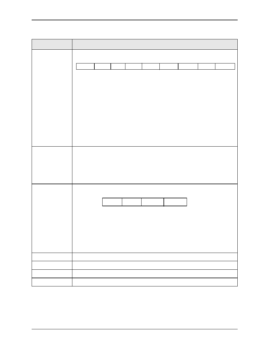
RS8234
5.0 Reassembly Coprocessor
ATM ServiceSAR Plus with xBR Traffic Management
5.7 Reassembly Control and Status Structures
28234-DSH-001-B
Mindspeed Technologies
TM
5-53
STATUS
Sets various status bits. The STATUS field contains the following control bits:
FFPD
= DMA FIFO buffer Full Packet Discard.
EPD
= Early Packet Discard occurred. A partially reassembled CPCS-PDU has been discarded
due to firewall, buffer underflow, LI_EPD, SN_EPD, ST_EPD, CLP discard or Max PDU
length exceeded.
FW
= Firewall error condition occurred. If early packet discard occurs, EPD is set.
UNDF
= Free Buffer Queue Underflow occurred. If early packet discard occurs, EPD is set.
OVFL
= Last available Status Queue entry.
SFPD
= Status Full Packet Discard occurred. EPD is not set.
TO
= Reassembly time-out condition occurred on this channel. EPD is not set.
ABORT
= Abort function detected. EPD not set.
CNT_ROVR = Indication that the SERVICE_CNT counter has rolled over on the channel or an AAL3/4
MIB counter has rolled over in an AAL3/4 Head VCC entry. If AAL3/4 MIB, then the
A3L2_ERR field is active in the PDU_CHECKS field and indicates which AAL3/4 MIB
counter has rolled over.
OAM
If this field is nonzero, it indicates that an OAM or management cell has been received as follows:
001 - F4 OAM
010 - F4 OAM End to End
100 - F5 OAM
101 - F5 OAM End to End
110 - PTI = 6
111 - PTI = 7
STM
Sets various bits related to Streaming Mode. The STM field contains the following control bits:
EOM
= In Streaming Mode or BOM Interrupt mode, this bit identifies that the buffer contains
an EOM.
BOM
= In Streaming Mode or BOM Interrupt mode, this bit identifies that the buffer contains a
BOM. In Message Mode with BOM interrupt enabled, indicates that status entry points
to only one buffer which contains a BOM.
STM_MODE = Indication that Streaming Mode is enabled on the channel.
BFR1
= In Streaming Mode, indicates which free buffer queue the buffer came from. Logic high
indicates COM(BFR1), logic low indicates BOM(BFR0).
FWD_PM
PM-OAM Forward Monitoring cell detected.
BIPV
BIP 16 violations. Same as BLER0+1 field in Backward Reporting PM-OAM cell.
TRCC0
PM total received cell count for CLP = 0.
TRCC0+1
PM total received cell count for CLP = 0+1.
Table 5-33. Reassembly Status Queue Entry Descriptions (2 of 2)
Field Name
Description/Function
EPD
FW
UNDF
OVFL
SFPD
TO
ABORT
CNT_ROVR
FFPD
16
15
14
13
12
11
10
9
8
EOM
BOM
STM_MODE
BFR1
3
2
1
0

5.0 Reassembly Coprocessor
RS8234
5.7 Reassembly Control and Status Structures
ATM ServiceSAR Plus with xBR Traffic Management
5-54
Mindspeed Technologies
TM
28234-DSH-001-B
5.7.6 LECID Table
The LECID Table illustrated in
Figure 5-18
includes up to 32 unique identifiers
for LAN Emulation Clients (LECIDs). The DPRI field in the reassembly VCC
Table entry is used as the index into this table.
Table 5-34
and
Table 5-35
display
the LECID Table entries and field definitions.
Figure 5-18. LECID Table, Illustrated
Top of VPI Index Table
DPRI
(Table holds 32 LECIDs)
LECIDn
LECIDn+
LECIDn+
LECIDn+
(etc.)
(etc.)
100074_039
Table 5-34. LECID Table Entries
Word 31 30 29 28 27 26 25 24 23 22 21 20 19 18 17 16 15 14 13 12 11 10 9
8
7
6
5
4
3
2
1
0
0
LECID1
LECID0
...
...
...
1-15
LECID31
LECID30
Table 5-35. LECID Table Field Definition
Field Name
Function/Description
LECIDn
LAN Emulation Client Identifier: a unique identifier for a LAN Emulation Client (LEC). The LECID
Table is capable of storing 32 LECIDs.
The system designer can initialize this table to contain the LECIDs of LAN Emulation Clients
that are transmitting multicast frames (point-to-multipoint Emulated LAN traffic) on an ATM
network. Thus, with the LECID_EN bit set to a logic high on a channel, the RSM Coprocessor
looks for a match in the LECID Table with the LECID in each received LANE frame, and if a
match, the frame is discarded. This implements echo suppression of superfluous
multi-broadcast LANE traffic on the ATM network.
RS8234
5.0 Reassembly Coprocessor
ATM ServiceSAR Plus with xBR Traffic Management
5.7 Reassembly Control and Status Structures
28234-DSH-001-B
Mindspeed Technologies
TM
5-55
5.7.7 Global Time-out Table
This table exists in internal SRAM starting at address 0x1340. The values in this
table should be initialized during system initialization, before reassembly
processing is started. These values set the selectable hardware PDU timeout
values as described in
Section 5.4.9
.
Table 5-36
and
Table 5-37
display the entries
and field definitions for the Global Time-out Table.
Table 5-36. Global Time-out Table Entry Format
Word
31 30 29 28 27 26 25 24 23 22 21 20 19 18 17 16 15 14 13 12 11 10 9
8 7 6
5 4 3
2 1 0
0
TERM_TOCNT1
TERM_TOCNT0
1
TERM_TOCNT3
TERM_TOCNT2
2
TERM_TOCNT5
TERM_TOCNT4
3
TERM_TOCNT7
TERM_TOCNT6
4
Reserved
TO_VCC_INDEX
Table 5-37. Global Time-out Table Entry Descriptions
Field Name
Description/Function
TERM_TOCNTx
Time-out expiration count.
TO_VCC_INDEX
Time-out VCC_INDEX tracking variable.

5.0 Reassembly Coprocessor
RS8234
5.7 Reassembly Control and Status Structures
ATM ServiceSAR Plus with xBR Traffic Management
5-56
Mindspeed Technologies
TM
28234-DSH-001-B
5.7.8 Reassembly Internal SRAM Memory Map
As indicated in
Table 5-38
, the Reassembly Internal SRAM is in the address
range 0x1000-0x13FF.
Table 5-38. Reassembly Internal SRAM Memory Map
Address
Name
Description
Internal Reassembly Status Queue Base Table Registers:
0x1000-0x1007
RSM_SQ_QU0
Status Queue 0 Base Table
0x1008-0x100F
RSM_SQ_QU1
Status Queue 1 Base Table
...
...
...
0x10F8-0x10FF
RSM_SQ_QU31
Status Queue 31 Base Table
Internal Reassembly Free Buffer Queue Base Table Registers:
0x1100-0x110F
RSM_FBQ_QU0
Free Buffer Queue 0 Base Table
0x1110-0x111F
RSM_FBQ_QU1
Free Buffer Queue 1Base Table
...
...
...
0x12F0-0x12FF
RSM_FBQ_QU31
Free Buffer Queue 31Base Table
Other Internal Reassembly Registers:
0x1300-0x133F
Reserved
0x1340-0x1353
GBL_TO
Global Time-out Table
0x1354-0x13FF
Reserved
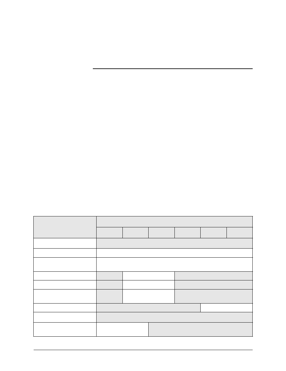
28234-DSH-001-B
Mindspeed Technologies
TM
6-1
6
6.0 Traffic Management
6.1 Overview
The traffic management capabilities of ATM differentiate it from other
communication technologies. The RS8234 xBR Traffic Manager implements the
complete set of ATM Service Categories as defined in the ATM Forum's Traffic
Management (TM) 4.1 Specification. These categories include CBR, Real-Time
and Non-Real-Time Variable Bit Rate (rt-VBR and nrt-VBR), UBR, GFR,
and ABR.
Table 6-1
provides a list of ATM attributes detailed in the TM 4.1
Specification (i.e., traffic parameters, QoS parameters, and feedback
characteristics), and identifies whether the RS8234 supports these for each
service category. The shaded areas are not indicative that the service category and
attribute are undefined for the SAR -- they simply indicate that the TM 4.1
Specification does not detail them.
Table 6-1. ATM Service Category Parameters and Attributes (1 of 2)
Attribute
ATM Layer Service Category
CBR
rt-VBR
(1)
nrt-VBR
(2)
UBR
(3)
ABR
GFR
TRAFFIC PARAMETERS:
Peak Cell Rate (PCR)
Specified/Supported
Cell Delay Variation Tolerance
(CDVT), at PCR
Supported
Sustainable Cell Rate (SCR)
Supported
Maximum Burst Size (MBS)
Supported
Cell Delay Variation Tolerance
(CDVT), at SCR
Supported
Minimum Cell Rate (MCR)
Supported
QOS PARAMETERS:
peak-to-peak Cell Delay Variation
(CDV)
Supported
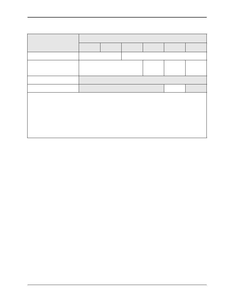
6.0 Traffic Management
RS8234
6.1 Overview
ATM ServiceSAR Plus with xBR Traffic Management
6-2
Mindspeed Technologies
TM
28234-DSH-001-B
In order to supply these services, the xBR Traffic Manager directs the
segmentation on each active VCC by controlling the segmentation coprocessor.
By intelligently selecting when each VCC transmits a cell, the Traffic Manager
guarantees that the output of the RS8234 conforms to the negotiated traffic
contract. This selection process (called Scheduling) executes dynamically, based
upon per-VCC parameters.
The xBR Traffic Manager consists of two primary components. The first is
the Dynamic Cell Scheduler, which provides for CBR, VBR, UBR, and GFR
traffic. Second, for ABR service classes, is the ABR Flow Control Manager, an
additional state machine, which works in conjunction with the xBR Cell
Scheduler.
Due to the complexities of ABR, a dedicated state machine is required to
achieve full rate performance � one which reacts to feedback from the network
and adjusts cell transmission accordingly. This specification models ABR to align
with the TM 4.1 ABR specification. The RS8234 supports the rate based flow
control and service models specified for ABR in TM 4.1.
The RS8234 also provides Generic Flow Control. This XON/XOFF protocol
complements the GFC algorithm by allowing switches to significantly
overallocate port bandwidth.
max Cell Transfer Delay (CTD)
Supported
(4)
Not Supported
(4)
Cell Loss Ratio (CLR)
Supported
(4)
Not
Supported
(
4)
Supported
(
4)
Not
Supported
(
4)
OTHER ATTRIBUTES:
Feedback
(5)
Supported
NOTE(S):
(1)
The rt-VBR service category is intended for real-time applications; i.e., those requiring tightly constrained delay and delay
variation, as would be appropriate for voice and video applications.
(2)
The nrt-VBR service category is intended for non-real-time applications which have bursty traffic characteristics.
(3)
The UBR service category is intended for non-real-time applications which do not require tightly constrained delay and delay
variation. Examples of such applications are traditional computer communications applications, such as file transfer and e-mail.
(4)
This is a network parameter. The RS8235 provides counters that monitor this parameter.
(5)
Feedback refers to the several types of control cells called Resource Management Cells (RM cells), which are conveyed back
to the source in order to control the source transmission rate in response to changing ATM layer transfer characteristics.
Table 6-1. ATM Service Category Parameters and Attributes (2 of 2)
Attribute
ATM Layer Service Category
CBR
rt-VBR
(1)
nrt-VBR
(2)
UBR
(3)
ABR
GFR
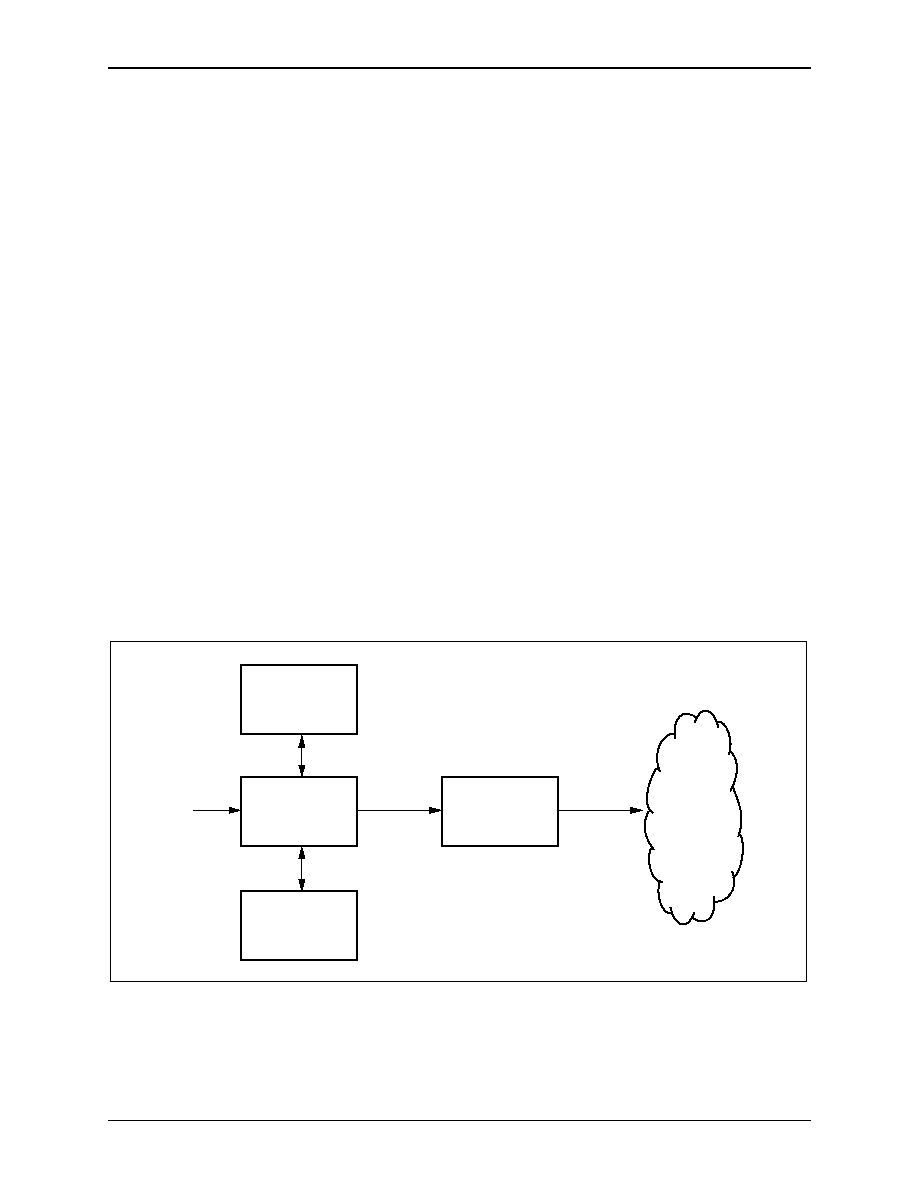
RS8234
6.0 Traffic Management
ATM ServiceSAR Plus with xBR Traffic Management
6.1 Overview
28234-DSH-001-B
Mindspeed Technologies
TM
6-3
6.1.1 xBR Cell Scheduler
The Cell Scheduler maintains the QoS guarantees for each service category. It
rate-shapes all segmentation traffic according to per-channel parameters. This
provides each channel with appropriate transmission opportunities and guarantees
conformance with network traffic contract policing algorithms applied to the
outputs.
The Cell Scheduler selects individual channels based upon the Dynamic
Schedule Table. Schedule Slots in this table may be pre-reserved for CBR
services. The VPs and VCs with CBR service reserve cell slots for transmission,
and are intended for highly regular data sources, such as voice circuits. The
RS8234 schedules all other traffic dynamically. The proprietary dynamic
scheduling algorithm uses the remaining bandwidth to statistically multiplex all
other service classes onto the line. The RS8234 can manage VCC traffic on either
a VC or a VP level. As well, it can schedule traffic as a CBR tunnel (or pipe), i.e.,
several VCCs assigned to a single CBR scheduling priority, with individual VCCs
within that tunnel scheduled based on their traffic parameters. Traffic into this
CBR tunnel can be of types UBR, VBR and ABR. To enhance flexibility, the
RS8234 supports 16 priorities of non-CBR traffic.
Figure 6-1
shows a high level block diagram of the Cell Scheduler control
flow for CBR, VBR, and UBR traffic. The Cell Scheduler tracks cell slots using
the system clock and decides which VCC should send during each slot. This
decision is based upon per-VCC parameters and the current condition of the
Dynamic Schedule Table. Unlike ABR, these service categories are open loop,
and need no feedback from the network for run-time cell scheduling.
Figure 6-1. Non-ABR Cell Scheduling
ATM
Network
Dynamic
Schedule
Table
xBR
Cell Scheduler
Per-VCC
Parameters
and Priority
Segmentation
Coprocessor
System
Clock
VCC_INDEX
CBR
VBR
UBR
GFR
100074_040
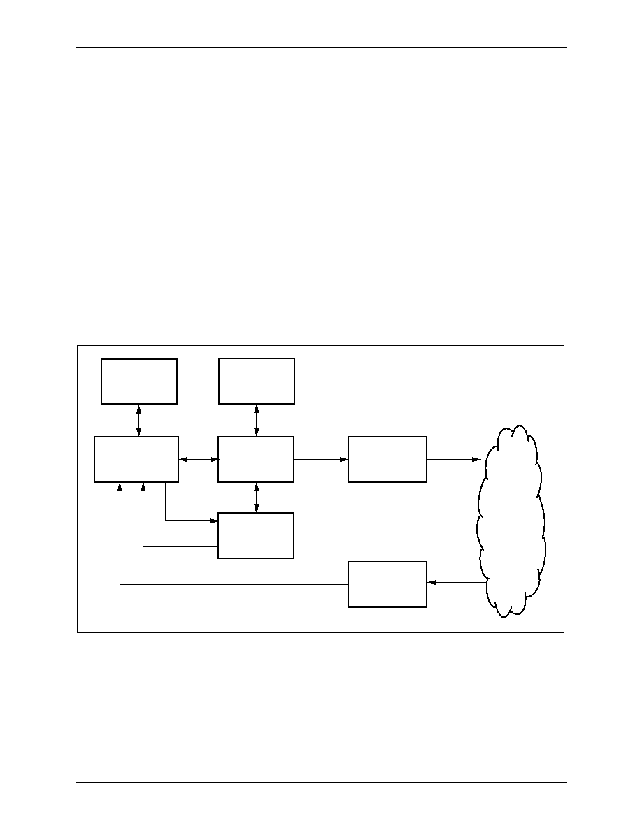
6.0 Traffic Management
RS8234
6.1 Overview
ATM ServiceSAR Plus with xBR Traffic Management
6-4
Mindspeed Technologies
TM
28234-DSH-001-B
6.1.2 ABR Flow Control Manager
The RS8234 implements the ATM Forum ABR flow control algorithms, referred
to in the aggregate as ABR by this document. The ABR service category
effectively allows zero cell loss transmission through an ATM network, by
regulating transmission based upon network feedback. The ABR algorithms
regulate the rate of each VCC independently.
Figure 6-2
shows a high level block
diagram of the RS8234's ABR feedback control loop.
Network feedback is received by the reassembly coprocessor and routed to the
ABR Flow Control Manager. This state machine processes the feedback
information according to per-VCC parameters and user programmable ABR
templates, both located in SAR shared memory. These templates define ABR
service parameters and policies for groups of VCCs.
Once the feedback is processed, the Flow Control Manager provides the Cell
Scheduler with an updated rate. Under the policy imposed by the template, the
rate complies with the TM 4.1 Source Behavior specifications. Until the next
update, the Cell Scheduler uses this rate to dynamically schedule the connection.
For optimal performance, the ABR Flow Control Manager implements the
ABR algorithm in a hardware state machine. However, to provide flexibility
against minor changes in the immature TM 4.1 specification, the state machine is
programmable through Mindspeed-supplied ABR templates. These templates,
resident in SAR shared memory, also provide a policy tuning mechanism for
interoperability and performance. Separate groups of VCCs can be assigned to
application optimized templates according to their path through the network.
Figure 6-2. ABR Flow Control
ATM
Network
ABR
Templates
ABR Flow Control
Manager
Dynamic
Schedule
Table
Cell Scheduler
Per-VCC
Parameters
and Priority
Segmentation
Coprocessor
Reassembly
Coprocessor
RATE
UPDATE
VCC_INDEX
ABR
Cell Stream
RM Cell
Feedback
100074_041

RS8234
6.0 Traffic Management
ATM ServiceSAR Plus with xBR Traffic Management
6.2 xBR Cell Scheduler Functional Description
28234-DSH-001-B
Mindspeed Technologies
TM
6-5
6.2 xBR Cell Scheduler Functional Description
6.2.1 Scheduling Priority
6.2.1.1 16 Priority
Levels + CBR
The RS8234 supports 16 scheduling priorities (the "PRI" field in the SEG VCC
Table entry), in addition to the optional CBR service category, with "15" being
the highest priority, down to "0" being the lowest priority. CBR channels are
assigned a priority which is in effect higher than the 16 scheduling priorities dis-
cussed here. From one to 16 of these scheduling priorities can be assigned to
VBR and ABR service classes. The others are shared UBR priorities. The
VBR/ABR priorities must be contiguous within the 16 scheduling priorities, and
thus accessible by an offset pointer. The host sets the offset of the VBR/ABR pri-
orities in the VBR_OFFSET field of SEG_CTRL or SCH_CTRL.
6.2.1.2 VCC Priority
Assignment
The host assigns the priority of all VCCs, except CBR VCCs, by setting the PRI
field in the Segmentation VCC Table Entry. This priority should be set at
connection setup and should not be changed dynamically.
6.2.2 Dynamic Schedule Table
6.2.2.1 Overview
The xBR Cell Scheduler schedules traffic according to the Dynamic Schedule
Table. The table contains a programmable number of slots, determined by
SCH_SIZE(TBL_SIZE). The duration of a single slot is a programmable number
of System Clocks, set as the number of system clocks per schedule slot, in
SCH_SIZE(SLOT_PER). The Cell Scheduler sequences through this table in a
circular fashion to schedule CBR, VBR, and ABR traffic. UBR traffic is handled
as described in
Section 6.2.5
. By configuring the number of slots and the duration
of each slot, the system designer chooses a range of available rates. This range of
available rates is dictated by the rate at which a single slot is scheduled, the size of
the table, and how many slots in the Dynamic Schedule Table each channel is
assigned.
APPLICATION EXAMPLE: Application-Specific Templates
Each template may have different flow control parameters. For instance, a system designer may
wish to configure a VCC traversing a network with all ER switches with a Rate Increase Factor
(RIF) and Rate Decrease Factor (RDF) = 1. However, a VCC traversing a network with switches
doing CI/NI (binary) marking will desire an RIF and RDF
1. Thus, separate templates would
be desired for these VCCs.

6.0 Traffic Management
RS8234
6.2 xBR Cell Scheduler Functional Description
ATM ServiceSAR Plus with xBR Traffic Management
6-6
Mindspeed Technologies
TM
28234-DSH-001-B
Figure 6-3
represents an example of a schedule table. In this example, the
system designer has chosen 100 schedule slots. The duration of each slot is a
programmable number of system clocks. The system designer may choose to
schedule cells close to the full payload data rate of STS-3C at 353.2 K
cells/second. At this cell rate, each cell slot will take 95 clocks. The scheduler
begins at slot 00 and increments its position in the table every 95 clocks. After
9,500 clocks, the scheduler position returns to 00.
6.2.2.2 Schedule Table
Slots
The user can select from a wide range of possible schedule slot formats. The user
selects a format based on system requirements. If the system needs to generate
CBR traffic, then the first 16 bits of each schedule table slot are reserved for a
CBR slot entry. The number of distinct VBR and ABR priorities required, and the
enabling of CBR traffic, govern the size requirements for each slot.
The USE_SCH_CTRL bit in the SEG_CTRL register is used to turn on and
turn off the mechanisms that create the 16 scheduling priorities. This maintains
backward compatibility to earlier versions of the SAR, where only eight
scheduling priorities were used.
Figure 6-3. Schedule Table with Size = 100
00
01
02
03
04
05
06
07
08
09
10
11
12
13
14
15
16
17
18
19
20
21
22
23
24
25
26
27
28
29
30
31
32
33
34
35
36
37
38
39
40
41
42
43
44
45
46
47
48
49
50
51
52
53
54
55
56
57
58
59
60
61
62
63
64
65
66
67
68
69
70
71
72
73
74
75
76
77
78
79
80
81
82
83
84
85
86
87
88
89
90
91
92
93
94
95
96
97
98
99
Cell Schedule
Starts @
Schedule Slot 00
Increments Postition by One Entry Each SLOT_PER
Current Cell
Scheduler Postion
29
Assigned
VCC_INDEX(es)
SLOT INDEX
1 or 2
Words
(4 or 8
Octets)
}
SCHEDULE SLOT
SCHEDULE TABLE
Scheduler Wraps Back
to 00 at End of Table
100074_042

RS8234
6.0 Traffic Management
ATM ServiceSAR Plus with xBR Traffic Management
6.2 xBR Cell Scheduler Functional Description
28234-DSH-001-B
Mindspeed Technologies
TM
6-7
If the USE_SCH_CTRL bit is asserted, the user controls the size and format
of all schedule slots through the SLOT_DEPTH, 4-bit VBR_OFFSET, and
TUN_PRI0-OFFSET fields in the SCH_CTRL register, as well as the CBR_TUN
bit in the SEG_CTRL register. If the USE_SCH_CTRL bit in the SEG_CTRL
register is not asserted, the user controls the size and format of all schedule slots
through the DBL_SLOT, 3-bit VBR_OFFSET, and CBR_TUN fields in the
SEG_CTRL register. These factors, coupled with the size of the Schedule Table,
determine the memory requirements for the Schedule Table.
Table 6-2
describes the parameters directly associated with the various
Schedule Table slot sizes.
Table 6-2. Selection of Schedule Table Slot Size by System Requirements
CBR
Service
Number of
VBR/ABR
Priorities
Required
Schedule Slot
Size
CBR_TUN
SLOT_DEPTH
Available VBR/ABR
Priority Levels
No
16
8 Words (256 bits)
0
111
0 thru 15
(1)
Yes
15
8 Words (256 bits)
1
111
1 thru 15
(1)
No
14
7 Words (224 bits)
0
110
VBR_OFFSET + 0 thru 13
Yes
13
7 Words (224 bits)
1
110
VBR_OFFSET + 1 thru 13
No
12
6 Words (192 bits)
0
101
VBR_OFFSET + 0 thru 11
Yes
11
6 Words (192 bits)
1
101
VBR_OFFSET + 1 thru 11
No
10
5 Words (160 bits)
0
100
VBR_OFFSET + 0 thru 9
Yes
9
5 Words (160 bits)
1
100
VBR_OFFSET + 1 thru 9
No
8
4 Words (128 bits)
0
011
VBR_OFFSET + 0 thru 7
Yes
7
4 Words (128 bits)
1
011
VBR_OFFSET + 1 thru 7
No
6
3 Words (96 bits)
0
010
VBR_OFFSET + 0 thru 5
Yes
5
3 Words (96 bits)
1
010
VBR_OFFSET + 1 thru 5
No
4
2 Words (64 bits)
0
001
(DBL_SLOT=1)
(2)
VBR_OFFSET + 0 thru 3
Yes
3
2 Words (64 bits)
1
001
(DBL_SLOT=1)
(2)
VBR_OFFSET + 1 thru 3
No
2
1 Word (32 bits)
0
000
(DBL_SLOT=0)
(2)
VBR_OFFSET + 0 or 1
Yes
1
1 Word (32 bits)
1
000
(DBL_SLOT=0)
(2)
VBR_OFFSET + 1
NOTE(S):
(1)
VBR_OFFSET would be set to zero for this mode of operation.
(2)
The bottom four rows of this table describe the slot size formats when USE_SCH_CTRL is not asserted.
6.0 Traffic Management
RS8234
6.2 xBR Cell Scheduler Functional Description
ATM ServiceSAR Plus with xBR Traffic Management
6-8
Mindspeed Technologies
TM
28234-DSH-001-B
6.2.2.3 Schedule Slot
Formats Without
USE_SCH_CTRL
Asserted
The VCC Index contents of each Schedule Table slot, based on the settings in
the last four rows of the table above, are illustrated in
Figure 6-4
. The SAR can
assign VBR VCC index(es) to any or all of the VBR VCC_Index fields in a
schedule table slot. Each of the VBR fields in a schedule table slot that are
assigned a VBR VCC_Index have a different scheduling priority (PRI), one from
the other. Also, any of these VBR VCC_Indexes assigned by the SAR can be the
first of a linked list of VBR VCCs.
VBR_OFFSET Described
VBR_OFFSET gives the offset difference in priority level between what the
user or system designer wishes to assign VBR channels and what the SAR assigns
via the VBR Schedule Slot format. Thus, the value of VBR_OFFSET is the
difference between the highest VBR/ABR priority being actively scheduled and
the largest priority of the VBR VCC_Index field in the VBR scheduling slot
(either one or three). For example, if the system designer assigns VBR/ABR
VCCs to three different scheduling priorities with the highest of those priorities
being "5" (i.e., PRI = 5), then:
VBR_OFFSET = 5 � 3 = 2.
Figure 6-4
illustrates how these priorities are assigned to the VBR fields.
Figure 6-4. Schedule Slot Formats With USE_SCH_CTRL Not Asserted
CBR
VCC_Index
VBR
VCC_Index
(PRI=VBR_OFFSET+1)
CBR
VCC_Index
VBR
VCC_Index
(PRI=VBR_OFFSET+1)
VBR
VCC_Index
(PRI=VBR_OFFSET+3)
VBR
VCC_Index
(PRI=VBR_OFFSET+0)
VBR
VCC_Index
(PRI=VBR_OFFSET+0)
VBR
VCC_Index
(PRI=VBR_OFFSET+2)
VBR
VCC_Index
(PRI=VBR_OFFSET+1)
VBR
VCC_Index
(PRI=VBR_OFFSET+1)
VBR
VCC_Index
(PRI=VBR_OFFSET+3)
VBR
VCC_Index
(PRI=VBR_OFFSET+2)
CBR_TUN = 1, DBL_SLOT = 0
CBR_TUN = 1, DBL_SLOT = 1
CBR_TUN = 0, DBL_SLOT = 0
CBR_TUN = 0, DBL_SLOT = 1
8236_107
= User Defined
NOTE(S):
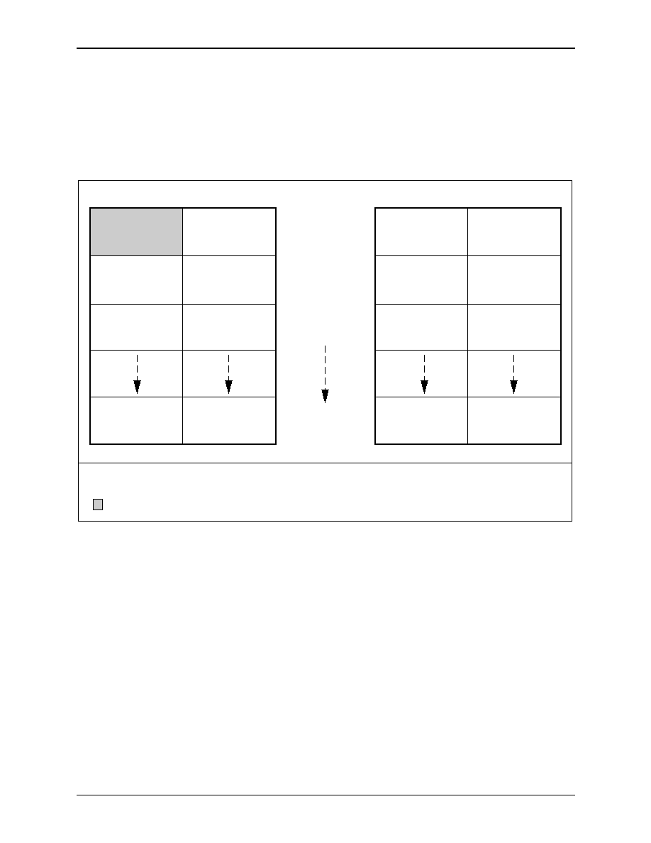
RS8234
6.0 Traffic Management
ATM ServiceSAR Plus with xBR Traffic Management
6.2 xBR Cell Scheduler Functional Description
28234-DSH-001-B
Mindspeed Technologies
TM
6-9
6.2.2.4 Schedule Slot
Formats With
USE_SCH_CTRL
Asserted
When USE_SCH_CTRL is asserted, the SLOT_DEPTH and VBR_OFFSET
fields in the SCH_CTRL register plus the CBR_TUN field in the SEG_CTRL
register, dictate the format of each schedule slot. This format is illustrated in
Figure 6-5
.
Figure 6-5. Schedule Slot Formats With USE_SCH_CTRL Asserted
CBR
VCC_Index
VBR/ABR
VCC_Index
(PRI=VBR_OFFSET+1)
VBR/ABR
VCC_Index
(PRI=VBR_OFFSET+3)
VBR/ABR
VCC_Index
(PRI=VBR_OFFSET+5)
VBR/ABR
VCC_Index
(PRI=15)
VBR/ABR
VCC_Index
(PRI=VBR_OFFSET+2)
VBR/ABR
VCC_Index
(PRI=VBR_OFFSET+4)
VBR/ABR
VCC_Index
(PRI=14)
(1)
(1)
VBR/ABR
VCC_Index
(PRI=VBR_OFFSET+1)
VBR/ABR
VCC_Index
(PRI=VBR_OFFSET+0)
VBR/ABR
VCC_Index
(PRI=VBR_OFFSET+3)
VBR/ABR
VCC_Index
(PRI=VBR_OFFSET+5)
VBR/ABR
VCC_Index
(PRI=15)
VBR/ABR
VCC_Index
(PRI=VBR_OFFSET+2)
VBR/ABR
VCC_Index
(PRI=VBR_OFFSET+4)
VBR/ABR
VCC_Index
(PRI=14)
(1)
(1)
CBR_TUN = 1
CBR_TUN = 0
SLOT_DEPTH = 000
SLOT_DEPTH = 001
SLOT_DEPTH = 010
SLOT_DEPTH = 111
8236_108
NOTE(S):
(1)
VBR_OFFSET would be set to 0 for these Schedule Slot formats.
= User Defined
6.0 Traffic Management
RS8234
6.2 xBR Cell Scheduler Functional Description
ATM ServiceSAR Plus with xBR Traffic Management
6-10
Mindspeed Technologies
TM
28234-DSH-001-B
6.2.2.5 Some
Scheduling Scenarios
This section discusses a few examples of scheduling priority schemes that system
designers may decide to implement, which demonstrate the range of flexibility
that the RS8234 affords system designers and network administrators.
Figure 6-6
illustrates how scheduling priorities are assigned in scheduling
slots. In this illustration, the number of VBR/ABR priorities = 3. In addition, the
tunnel at PRI=5 has shared VBR traffic. CBR_TUN = 1, SLOT_DEPTH = 001.
The highest VBR/ABR scheduling priority (PRI) is 5. Thus, VBR_OFFSET = 1.
As mentioned before, the VBR/ABR priorities must be contiguous in order to
be accessible by VBR_OFFSET. To ensure that these priorities remain contiguous
when accessed by VBR_OFFSET, the following condition must be met:
VBR_OFFSET + (# of VBR/ABR priorities)
<
15
Figure 6-6. One Possible Scheduling Priority Scheme with the RS8234
CBR
Reserved for Tunnel 1
UBR1
VBR1
VBR2
ABR
UBR2
UBR3
Reserved for Tunnel 2
Service/Application
Scheduling Priority
High
Low
Voice -- AAL1 on AAL0 VCCs
Tunnel through public ATM Network
Signalling, ILMI, PNNI Traffic
rt-VBR -- Video
nrt-VBR -- Frame Relay/ABR
MCR
ABR>MCR -- LAN Data Traffic
High Priority UBR User Traffic
Low Priority UBR User Traffic
Tunnel through private ATM Network
7
6
5
4
3
2
1
0
VBR_OFFSET
= 1
(VBR/ABR Priority 1)
(VBR/ABR Priority 2)
(VBR/ABR Priority 3)
15
8
(Unused)
(Scheduling Priorities 8 thru 15
are not used in the scheme.)
(UBR Only)
(UBR & VBR shared)
100074_045

RS8234
6.0 Traffic Management
ATM ServiceSAR Plus with xBR Traffic Management
6.2 xBR Cell Scheduler Functional Description
28234-DSH-001-B
Mindspeed Technologies
TM
6-11
6.2.3 CBR Traffic
The CBR service category guarantees end-to-end bandwidth through the network.
Certain data sources, such as voice circuits, require this guarantee, as well as
constrained Cell Delay Variation (CDV). CDV is a measure of the "burstiness" of
traffic. The ATM network supplies a minimum CDV for CBR channels by
reserving cell transmission opportunities for the connections.
The RS8234 generates CBR traffic by assigning specific slots in the Schedule
Table to a CBR VCC. This connection will always send a single cell during its
assigned slots. The system clock serves as a time reference for CBR cell
generation. The systems designer programs the duration of schedule slots in
system clocks in the SLOT_PER (slot period) field of the SCH_SIZE register.
6.2.3.1 CBR Rate
Selection
Maximum Rate
For each CBR assigned cell slot, the RS8234 generates one cell on the specified
VCC. The maximum or base rate of CBR channels is determined by the duration
of a cell slot according to the equation below, where R
max
is the maximum rate in
cells per second.
SLOT_PER should be nominally set to the number of clock cycles needed to
transmit a full cell, and its minimum bound should be no less than 70.
6.2.3.2 Available Rates
Once a maximum rate
(R
max
)
has been selected, the size of the Schedule Table
determines the rate granularity and minimum rate. The system designer specifies
the number of table slots in SCH_SIZE(TBL_SIZE). The available CBR rates are:
R
max
, R
max
x(TBL_SIZE �1)/TBL_SIZE, R
max
x(TBL_SIZE � 2)/
TBL_SIZE, ... ..., R
max
/TBL_SIZE
Minimum Rate
The minimum rate available is therefore
R
max
/TBL_SIZE
.
SLOT_PER
frequency SYSCLK
(
)
R
m ax
------------------------------------------------------
=
APPLICATION EXAMPLE: Determining Maximum Rate
frequency(SYSCLK) = 33 MHz
SLOT_PER = 93 clocks/slot
R
max
= 354.8 K cells/second
To achieve the maximum rate, the user would assign one VCC to every cell slot in the Schedule Table.
This would prevent any other VCC from being scheduled since this channel uses all of the available
slots.
6.0 Traffic Management
RS8234
6.2 xBR Cell Scheduler Functional Description
ATM ServiceSAR Plus with xBR Traffic Management
6-12
Mindspeed Technologies
TM
28234-DSH-001-B
Assigning CBR Cell Slots
Figure 6-7
displays an example Schedule Table with slots assigned to various
CBR channels, each with a different rate. In this example, TBL_SIZE = 100 and
SLOT_PER = 93. VCC_INDEX A occupies every tenth schedule slot and
therefore it will transmit at R/10, or 35.4 K cells/second. VCC_INDEX B
occupies a slot every 25 cell slots and will transmit at a rate of R/25, or
14.2 K cells/second. VCC_INDEX C occupies only one schedule slot
and therefore will transmit at the minimum rate, R/TBL_SIZE, or
3.54 K cells/second. Not all cell slots have been assigned to CBR channels.
During these slots, the RS8234 will dynamically schedule traffic from the other
service classes. However, the total bandwidth of channels A, B, and C will be
reserved.
Figure 6-7. Assigning CBR Cell Slots
00
01
02
03
04
05
06
07
08
09
10
11
12
13
14
15
16
17
18
19
20
21
22
23
24
25
26
27
28
29
30
31
32
33
34
35
36
37
38
39
40
41
42
43
44
45
46
47
48
49
50
51
52
53
54
55
56
57
58
59
60
61
62
63
64
65
66
67
68
69
70
71
72
73
74
75
76
77
78
79
80
81
82
83
84
85
86
87
88
89
90
91
92
93
94
95
96
97
98
99
29
VCC_INDEX = B
SCHEDULE SLOT
SCHEDULE TABLE
A
A
A
A
A
A
A
A
A
A
B
B
B
B
B
C
100074_046
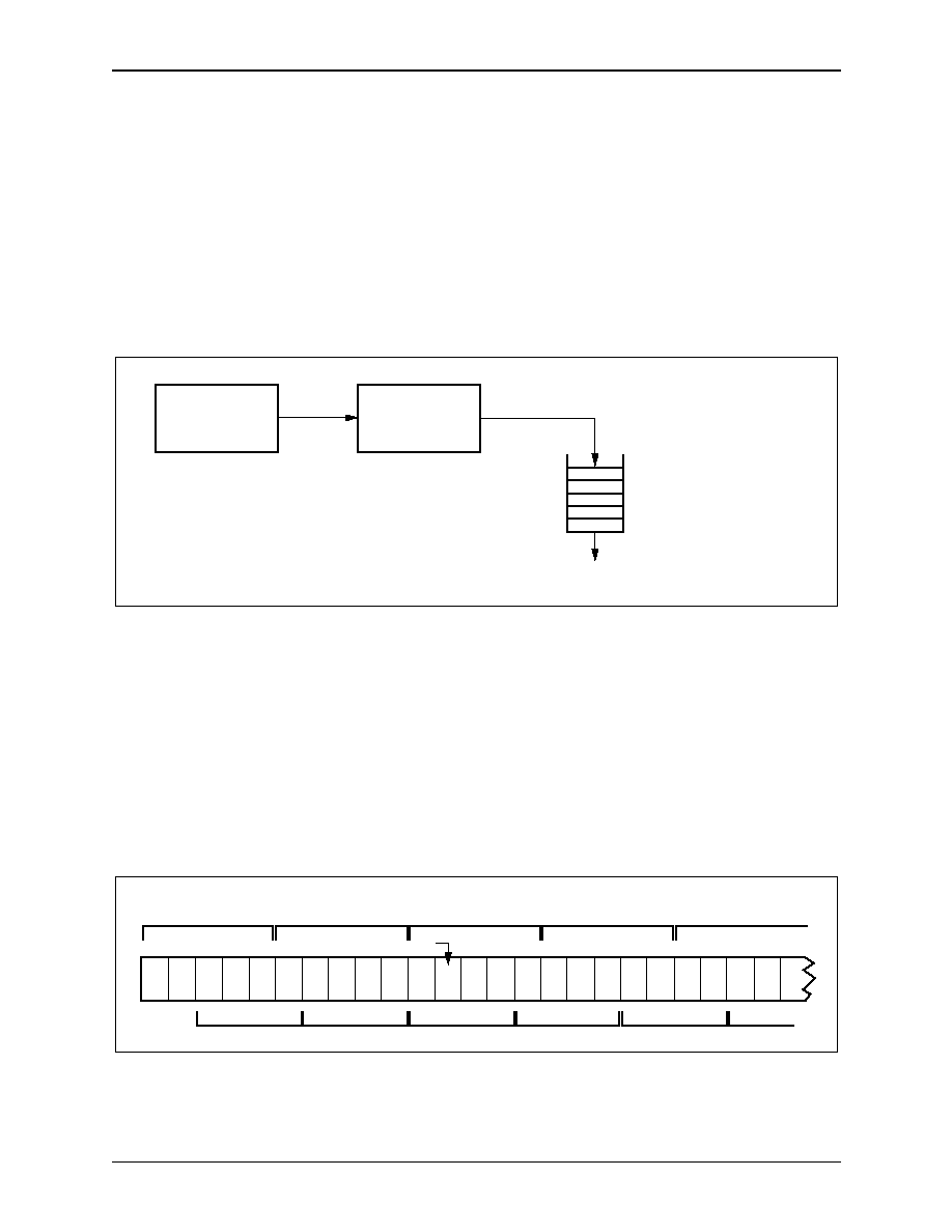
RS8234
6.0 Traffic Management
ATM ServiceSAR Plus with xBR Traffic Management
6.2 xBR Cell Scheduler Functional Description
28234-DSH-001-B
Mindspeed Technologies
TM
6-13
6.2.3.3 CBR Cell Delay
Variation (CDV)
By definition, CBR connections are sensitive to CDV. (See ATM Forum UNI 3.1
or TM 4.1 for a complete definition of CDV.) The RS8234's Traffic Manager
minimizes CDV by basing all traffic management on the SYSCLK frequency, and
providing the user the ability to explicitly decide the transmit time for CBR
traffic. However, no system is without some CDV. In the case of terminals using
the RS8234, the dominant factor in CDV is the variation introduced between the
segmentation coprocessor and the PHY layer device at the Transmit FIFO
(TX_FIFO). Line overhead created by the framer in the PHY layer device causes
this variation.
Figure 6-8
illustrates this interface.
A possible source of Schedule-Table-dependent CDV is created when the host
contracts for different CBR rates on more than one CBR channel, causing
schedule slot conflicts in the Schedule Table.
Figure 6-9
illustrates an example of
this. Illustrated is a linear representation of a Schedule Table with 100 schedule
slots. CBR channel A has reserved bandwidth for a rate of 70. K cells/second, or
every fifth cell slot. CBR channel B has reserved bandwidth for a rate of 88.7 K
cells/second, or every fourth cell slot. In this case there will be a schedule slot
reservation conflict between channels A and B every 20th cell slot, and one of the
channel's slots will have to be reserved one slot later.
Figure 6-8. Introduction of CDV at the ATM/PHY Layer Interface
Cell Scheduler
Segmentation
Coprocessor
Cells are added at CBR rate
Cells are removed at
(Line rate -- Line overhead)
PHY Interface
TX_FIFO
(1-9 Cells)
100074_047
Figure 6-9. Schedule Table with Slot Conflicts at Different CBR Rates
00
01
02
03
04
05
06
07
08
09
10
11
12
13
14
15
16
17
18
19
20 21
22
23
Schedule Table
A
A
A
A
A
B
B
B
B
B
B
5
5
5
5
4
4
4
4
4
100074_048

6.0 Traffic Management
RS8234
6.2 xBR Cell Scheduler Functional Description
ATM ServiceSAR Plus with xBR Traffic Management
6-14
Mindspeed Technologies
TM
28234-DSH-001-B
Another possible source of Schedule-Table-dependent CDV comes about for
certain CBR rates whose schedule slot spacings do not evenly divide the table slot
size. An example of this is illustrated in
Figure 6-10
. In this example, the
beginning and end of a 100 slot Schedule Table is shown. The system designer
has reserved bandwidth for CBR channel C at a rate of 32.25 K cells/second, or
every ninth cell slot. When the Scheduler wraps from the end of the table to the
beginning of the table, the number of schedule slots between the last C channel
slot at the end of the table and the first C channel slot at the beginning of the table
is 10 slots, not 9.
The worst-case CDV is determined by the following formula:
The first term in the formula above is introduced by CBR Rate Matching (see
Section 6.2.2.4
).
The second term in the formula above is introduced by the TX_FIFO itself.
The FIFO buffer introduces worst case CDV when one CBR cell is transmitted
through an empty FIFO buffer, and the next CBR cell from that channel is
segmented to a full FIFO buffer.
The system designer programs the TX_FIFO_LEN in the SEG_CTRL
register. By reducing the TX_FIFO_LEN, the system designer reduces CDV.
However, the TX_FIFO also absorbs PCI bus latency. To prevent PCI latency
from impacting line utilization, set the TX_FIFO length according to the
following formula:
Figure 6-10. CDV Caused by Schedule Table Size at Certain CBR Rates
00
01
02
03
04
05
06
07
08
09
10
11
12
13
14
15
16
17
18
19
20
85
86
87
88
89
90
91
92
93
94
95
96
97
98
99
Schedule Table
C
C
C
C
9
9
9
9
9
(Scheduler wraps
from slot 99 to slot 00.)
100074_049
CDV
max
1 (CBR rate in cells sec)
/
TX_FIFO_LEN (line rate in cells sec)
/
/
+
/
=
TX_FIFO_LEN > 1
(worst case PCI latency) (line rate in cells sec)
/
/
+

RS8234
6.0 Traffic Management
ATM ServiceSAR Plus with xBR Traffic Management
6.2 xBR Cell Scheduler Functional Description
28234-DSH-001-B
Mindspeed Technologies
TM
6-15
6.2.3.4 CBR Channel
Management
The host initializes the segmentation VCC Table entry of a CBR VCC. The
SCH_MODE of the VCC should be set to 001 (CBR). Thereafter, the RS8234
ignores further processing based on the SCH_MODE field in the VCC Table
entry for CBR VCCs.
CBR PVC Provisioning
Once a Schedule Table has been created, the system assigns specific cell slots to
any CBR provisioned virtual connections (PVCs). This process takes place before
the segmentation process is initiated. Once segmentation has begun, the RS8234
will dynamically allocate these cell slots to other channels until the data is
supplied for the CBR VCC.
CBR SVC Setup and Teardown
It is also possible to set up and tear down CBR switched virtual connections
(SVCs) without disrupting ongoing segmentation. The user simply configures a
new VCC Table entry. Once the VCC is initialized, the host assigns schedule slots
to the VCC according to its rate. The host then submits data as with any
segmentation VCC.
CBR Rate Matching
In reality, the CBR schedule rate of a channel will not exactly match the rate of its
data source. To compensate for this asynchronous data source behavior, the
RS8234 provides a rate matching mechanism for use when CBR traffic is mapped
to a Virtual FIFO. (This method is needed only for Virtual FIFOs. For VCCs that
are not Virtual FIFOs, the cell transmission is skipped automatically if there is no
data available.)
For an individual CBR channel mapped to a Virtual FIFO, the host directs the
RS8234 to skip one cell transmission opportunity whenever data is unavailable.
The host requests this rate matching adjustment by setting the SCH_OPT bit of
the CBR channel. The next time the RS8234 encounters a CBR slot for this VCC,
it will not transmit data on that VCC. Then the RS8234 indicates to the host that a
slot has been skipped by clearing the SCH_OPT bit.
With this method, the host effectively synchronizes the RS8234's scheduled
rate to the external data source rate. The host must configure the CBR VCC rate
slightly higher than the actual rate of the data source. Skipping cell transmission
slots then compensates for the rate differential.
6.0 Traffic Management
RS8234
6.2 xBR Cell Scheduler Functional Description
ATM ServiceSAR Plus with xBR Traffic Management
6-16
Mindspeed Technologies
TM
28234-DSH-001-B
6.2.4 VBR Traffic
The RS8234 Cell Scheduler also supports multiple priority levels for VBR traffic.
The VBR service class takes advantage of the asynchronous nature of ATM by
reserving bandwidth for VBR channels at average cell transmission rates without
hardcoding time slots, as with CBR traffic. This dynamic scheduling allows VBR
traffic to be statistically multiplexed onto the ATM line, resulting in better use of
the shared bandwidth resources.
6.2.4.1 Mapping
RS8234 VBR Service
Categories to TM 4.1
VBR Service Categories
The ATM Forum TM 4.1 Specification describes the different categories of VBR
service in a different manner than is employed in the RS8234 device. These
relationships are described here:
6.2.4.2 Rate-Shaping
vs. Policing
The Cell Scheduler rate-shapes the segmentation traffic for up to 64 K
connections. The outgoing cell stream for each VCC is scheduled according to
the GCRA algorithm. This guarantees compliance to policing algorithms applied
at the network ingress point. Channels can be rate-shaped as VCs or VPs,
according to one of three leaky bucket paradigms, set by the SCH_MODE bit in
the channel's segmentation VCC Table entry.
6.2.4.3 Single Leaky
Bucket
The first and simplest bucket scheme is single leaky bucket. The user defines a
single set of GCRA parameters -- I (Interval) and L (Limit). I is used to control
the per-VCC PCR and L is used to control the CDVT of the outgoing cell stream.
The user enables this scheme by setting the SCH_MODE bits to "
100
" (VBR1).
6.2.4.4 Dual Leaky
Bucket
The user can also select, on a per-VCC basis, to apply two leaky buckets to a
single connection. The user enables this scheme by setting the SCH_MODE bits
to "
101
"(VBR2).
When using VBR2 SCH_MODE, you are limited to 256 values for the I2 and
L2 parameters. These parameters are stored as bucket table entries. (See
Table 6-15
for the definition of a bucket table entry.) There is complete flexibility
with regard to using these 256 values to specify SCR or PCR. In VBR2, I1 and L1
can specify either PCR and CVDT, or SCR and Burst Tolerance (BT), with I2 and
L2 used to specify the parameters not assigned to I1 and L1.
For example, you can configure:
I1 = PCR, L1 = CDVT, I2 = SCR, L2 = BT
or
I1 = SCR, L1 = BT, I2 = PCR, L2 = CDVT
Table 6-3. RS8234 VBR to TM 4.1 VBR Mapping
RS8234 VBR
TM 4.1 VBR
Comments
VBR1
(None)
TM 4.1 does not employ single
leaky bucket.
VBR2
VBR.1
Double leaky bucket.
VBR3 (or VBRC)
VBR.2 /VBR.3
TM 4.1 defines two conformance standards for
CLP(0+1).

RS8234
6.0 Traffic Management
ATM ServiceSAR Plus with xBR Traffic Management
6.2 xBR Cell Scheduler Functional Description
28234-DSH-001-B
Mindspeed Technologies
TM
6-17
6.2.4.5 CLP-Based
Buckets
The third option allows both buckets to apply to CLP=0 cells. CLP=0 means high
priority cells; CLP=1 means cells are subject to discard. CLP=1 cells are
scheduled from the second bucket only. Therefore, the second bucket should
correspond to PCR. This controls the PCR of the total cell stream, but only
controls the SCR of CLP=0 cells. The user enables this scheme by setting the
SCH_MODE bits to "
110
" (VBRC -- also called VBR3).
6.2.4.6 Rate Selection
The I and L parameters of the GCRA algorithm represent cell slots in the
schedule table. Therefore, the VBR channels have the same maximum rate
available as the CBR channels. Since VBR channels are internally scheduled by
the Cell Scheduler based on that channel's I parameter, a floating point value, they
are not constrained to repeat at some n integer value of R
max
/(TBL_SIZE � n),
Thus, VBR channels have a much finer rate granularity.
The minimum rate for VBR channels is R
max
/(TBL_SIZE �1).
6.2.4.7 Real-Time VBR
and CDV
Real-time VBR traffic should be assigned the highest scheduling priority to
minimize cell delay variation. The worst-case CDV for rt-VBR traffic is
calculated as:
((# VBR VCCs at same-or-higher priority)+TX_FIFO_LEN)/(line rate in cells/sec).
6.2.5 UBR Traffic
The remaining priority levels not already assigned to ABR, VBR or CBR tunnel
traffic, are scheduled as UBR traffic. All UBR channels within a priority are
scheduled on a round-robin basis.
To limit the bandwidth that a UBR priority consumes, the user can use a CBR
tunnel in that priority level. Another method of limiting the bandwidth that a
UBR priority consumes is described in
Section 6.2.8
.

6.0 Traffic Management
RS8234
6.2 xBR Cell Scheduler Functional Description
ATM ServiceSAR Plus with xBR Traffic Management
6-18
Mindspeed Technologies
TM
28234-DSH-001-B
6.2.6 xBR Tunnels (Pipes)
A CBR tunnel occupies schedule table slots in the same manner as a CBR VCC.
However, instead of serving one VCC, from one to four priority levels are served.
The VCCs within a CBR tunnel can be UBR, VBR (VBR1 or VBR2), and/or
ABR traffic. In the case of a UBR priority in a tunnel, the VCCs of the served
priority level are serviced in round-robin order. For any VBR/ABR priorities in a
tunnel, each VCC is shaped to its GCRA parameters within the CBR tunnel.
NOTE:
The format of a CBR tunnel schedule table slot is not backward-
compatible with the CBR tunnel format used in the Bt8233 SAR.
When the user establishes a CBR tunnel, the user-defined transmit bandwidth
for that tunnel is reserved in the schedule table as schedule slots. The one-to-four
priority levels assigned to that tunnel are named at this time, and are written to the
PRI3, PRI2, PRI1, and PRI0 fields in the CBR_TUN_ID field for the schedule
slots reserved. PRI3 should specify the highest priority level for that tunnel, down
to PRI0 as the lowest assigned priority level for that tunnel. The scheduler
services the highest priority level that has data available on that priority queue at
each point a schedule slot for that tunnel becomes active. This serves as a
secondary shaping of the traffic assigned to these tunnel priorities. Any one
priority level can be assigned to only one CBR tunnel, and must not be assigned
as a priority to more than one tunnel. Additionally, all priority levels utilized
within a CBR tunnel need to be activated as a tunnel by setting the
TUN_ENA( � ) bit(s) in the SCH_PRI and SCH_PRI2 registers.
Sixteen tunnels can be active at once, if each of these tunnels has only one
scheduling priority assigned. All can be VBR/ABR tunnels. On the other hand,
the system designer can establish four tunnels, each of which has four scheduling
priorities assigned to it, or any combination of tunnels, which includes up to a
total of 16 scheduling priorities. Individual VCCs are assigned to the tunnel by
the host, by setting the PRI field in the VCC table to the priority of the tunnel.
The 3-bit PRI0 field allows the entry of only priority levels 0�7. If you wish to
enter a priority level higher than priority 7 in PRI0, you should assign the
difference in values as an offset, in the TUN_PRI0_OFFSET field in the
SCH_CTRL register.
If both non-tunnel and tunnel scheduling priorities exist, the host must assign
the highest priority level(s) to CBR tunnel(s).

RS8234
6.0 Traffic Management
ATM ServiceSAR Plus with xBR Traffic Management
6.2 xBR Cell Scheduler Functional Description
28234-DSH-001-B
Mindspeed Technologies
TM
6-19
APPLICATION EXAMPLES: Tunnels
Figure 6-6
shows priorities five and six used as CBR tunnels for UBR and VBR traffic. The host assigns
a fixed number of Schedule table slots to the tunnel to reserve a fixed rate. Each time an assigned slot is
encountered by the Cell Scheduler, it selects a VCC from a round-robin queue of active VCCs assigned to
that priority.
For example, 100 UBR VCCs with PRI = 6 might currently be segmenting data. Each gets 1/100th of the
CBR bandwidth assigned to the tunnel. Tunneling enables system-level end users to purchase CBR services
from a WAN service provider. The purchaser can then dynamically manage the traffic within this leased CBR
tunnel as CBR and/or a combination of other service categories.
In this example, the user has configured the RS8234 to manage two independent tunnels. The first tunnel
priority five, is through a private ATM network, perhaps a corporate ATM campus backbone. The other
tunnel, priority six, carries traffic through a public network. This topology allows the end user to lease
reserved CBR bandwidth from an administrative domain, but manage the usage of the tunnel in an arbitrary
fashion.
Figure 6-11
illustrates a different use of CBR tunnels. In this example, the user has established 4 separate
tunnels or pipes. Each can have an equal 1/4 share of the bandwidth available to the port by provisioning
every fourth schedule table slot to one tunnel for each of the four tunnels.
In each of the tunnels, 4 priority levels are assigned. The highest priority in each tunnel is assigned to
real-time VBR, the next highest priority to non-real-time VBR, the third highest priority to ABR, and the
lowest priority to UBR. This in effect establishes four multi-service pipes, each on equal priority to the others
(since the scheduler services each of the four pipes equally). Thus, the 4 rt-VBR priorities have effectively
the same priority, and so on through the four levels of priority serviced in each pipe. Number of VBR/ABR
priorities is 12. CBR_TUN = 1, SLOT_DEPTH = 110.
Highest VBR/ABR Scheduling priority is 15 (that is, PRI = 15). Thus, VBR_OFFSET = 3.
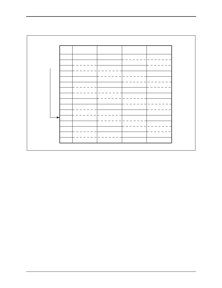
6.0 Traffic Management
RS8234
6.2 xBR Cell Scheduler Functional Description
ATM ServiceSAR Plus with xBR Traffic Management
6-20
Mindspeed Technologies
TM
28234-DSH-001-B
Figure 6-11. Another Possible Scheduling Priority Scheme with the RS8234
0
1
2
3
4
5
6
7
8
9
10
11
12
13
14
15
Tunnel A
Tunnel B
Tunnel C
Tunnel D
Priority
Levels
HIGH
VBR_OFFSET
=3
LOW
rt-VBR
nrt-VBR
nrt-VBR
nrt-VBR
nrt-VBR
rt-VBR
rt-VBR
rt-VBR
ABR
ABR
ABR
ABR
UBR
UBR
UBR
UBR
Example of Multi-Service Tunnels
100074_050

RS8234
6.0 Traffic Management
ATM ServiceSAR Plus with xBR Traffic Management
6.2 xBR Cell Scheduler Functional Description
28234-DSH-001-B
Mindspeed Technologies
TM
6-21
6.2.7 Guaranteed Frame Rate
GFR is a new service category defined by the ATM Forum to provide an MCR
QoS guarantee for AAL5 CPCS-PDUs (or "frames") not exceeding a specified
frame length. This class of service is designed specifically to use the UBR service
category. A GFR service connection is thus treated as UBR with a guaranteed
MCR.
The RS8234 implements GFR by scheduling/shaping the connections using
both the VBR1 scheduling procedure (for the MCR rate value) and a UBR
priority queue, thereby providing fair sharing for all GFR connections to excess
bandwidth. The VBR1 queue priority (the PRI field in the SEG VCC Table entry)
should be set to a higher priority than the UBR queue (the GFR_PRI field in the
SEG VCC table entry). The priority level entered in the GFR_PRI field can only
be one of the lower eight scheduling priorities. This establishes the condition
where those GFR connections sharing the same GFR_PRI would fair-share any
excess bandwidth above the MCR limits. Call control must be sure not to
oversubscribe MCR on GFR channels and other rate-guaranteed services.
The RS8234 helps guarantee MCR on a GFR channel by providing a
mechanism to trigger an increase in the scheduling priority by one priority level,
if the transmit rate on that channel falls below its specified MCR. This is done
using the MCRLIM_IDX field in that VCC's SCH_STATE entry in the SEG
VCC Table entry. MCRLIM_IDX is an 8-bit index into a table containing 256
entries (each formatted as described in
Table 6-19
), each containing MCR limit
values, and each indicating a trigger point for an increase in the VCC's priority for
that scheduled slot.
To disable this priority bumping, set MCR_LIMIT to its maximum value. The
user can accomplish this by setting each of the values in the GFR MCR Limit
bucket table entries as follows:
1.
Set NONZERO bits to 1.
2.
Set MCR_EXP fields to decimal value of 31 (i.e., all-ones).
3.
Set MCR_MAN fields to decimal value of 511 (i.e., all-ones).
An additional level of traffic shaping can be established on GFR-UBR priority
queues by shaping to a specified PCR. (See
Section 6.2.8
.)
6.2.8 PCR Control for Priority Queues
The RS8234 provides an optional method of creating tunnels (i.e., of limiting the
bandwidth of a group of channels), by allowing the user to assign a PCR to a
scheduling priority queue, so that the aggregate of the rates of the channels
assigned to that priority queue will not be greater than the PCR assigned. This can
be done for UBR, VBR, ABR and UBR-GFR traffic classes.
A maximum of four of the sixteen priority queues can be shaped to a PCR less
than line rate. The queues to be shaped are identified using the QPCR_ENAx bits
in the SCH_PRI and SCH_PRI_2 registers. The associated PCR for each queue
thus enabled is specified in one of the two PCR_QUE_INTxx registers. These
PCR values are stored as schedule table intervals. QPCR_INT3 maps to the
highest priority queue that is enabled for PCR shaping, QPCR_INT2 to the next
highest priority PCR shaped queue, and so on. If only one priority queue is
enabled for PCR shaping, it will be shaped using the QPCR_INT3 value; if two
priority queues are enabled for PCR shaping, QPCR_INT3 and QPCR_INT2 will
be used; and so on.
6.0 Traffic Management
RS8234
6.3 ABR Flow Control Manager
ATM ServiceSAR Plus with xBR Traffic Management
6-22
Mindspeed Technologies
TM
28234-DSH-001-B
6.3 ABR Flow Control Manager
6.3.1 A Brief Overview of TM 4.1
This section briefly describes the TM 4.1 ABR Flow Control algorithms.
However, it is strongly recommended that the reader be familiar with the ATM
Forum's TM 4.1 specification before attempting to understand the RS8234's ABR
implementation.
6.3.2 Internal ABR Feedback Control Loop
As a complete implementation of the UNI ATM layer, the RS8234 acts as both an
ABR Source and Destination, complying with all required TM 4.1 ABR
behaviors. The RS8234 utilizes the dynamic rate adjustment capability of the
xBR Cell Scheduler as the Source's variable rate shaper. An internal feedback
mechanism supplies feedback from the received cell stream to the ABR Flow
Control Manager, a special purpose state machine. This state machine translates
the feedback extracted from received Backward RM cells, to instructions for the
xBR Cell Scheduler and segmentation coprocessor. It supports both binary and
ER flow control methods.
Figure 6-12
illustrates this basic concept.
Figure 6-12. ABR Service Category Feedback Control
Source
Destination
Variable
Rate
Shaping
BW_RM
(Backward_RM)
TA_RM
(TurnAround_RM)
FW_RM
(ForWard_RM)
Switch
Congestion
Algorithms
ATM
Network
(
�
1 Switches)
Internal Congestion
Backpressure
100074_051

RS8234
6.0 Traffic Management
ATM ServiceSAR Plus with xBR Traffic Management
6.3 ABR Flow Control Manager
28234-DSH-001-B
Mindspeed Technologies
TM
6-23
6.3.2.1 Source Flow
Control Feedback
Figure 6-13
illustrates the feedback loop which controls the Source cell stream.
The RS8234 injects an in-rate cell stream (CLP = 0) into the ATM network for
each ABR VCC. Network elements modify the flow control fields in the cell
stream's Forward RM cells. After a round trip through the network and
destination node, these cells return to the RS8234 receive port as Backward RM
cells. The reassembly coprocessor processes incoming Backward RM cells, and
communicates with the segmentation state machines via the RSM/SEG Queue in
SAR shared memory. Upon receiving this feedback from the queue, the ABR
Flow Control Manager updates fields within the SCH_STATE portion of the
segmentation VCC Table entry. The xBR Cell Scheduler and segmentation
coprocessor use these fields to generate the ABR in-rate cell stream, closing the
Source Behavior feedback loop.
The SAR also processes the Explicit Forward Congestion Indication (EFCI)
bit in the data cell header(s) per the rules in TM 4.1.
Figure 6-13. RS8234 ABR-ER Feedback Loop (Source Behavior)
BACKWARD_RM
Segmentation
Reassembly
RS8234 Subsystem
ABR
Decision
Templates
Schedule
Table
ABR
Flow Control
Manager
Cell
Scheduler
Segmentation
Coprocessor
Rate
Decision
Reassembly
Coprocessor
RSM VCC
Table
Entry
SAR
UNI
ATM
Network +
Destination
Cell Type
Decision
RSM/SEG
Queue
ABR
Cell Stream
SEG VCC
Table Entry
SCH_STATE
100074_052
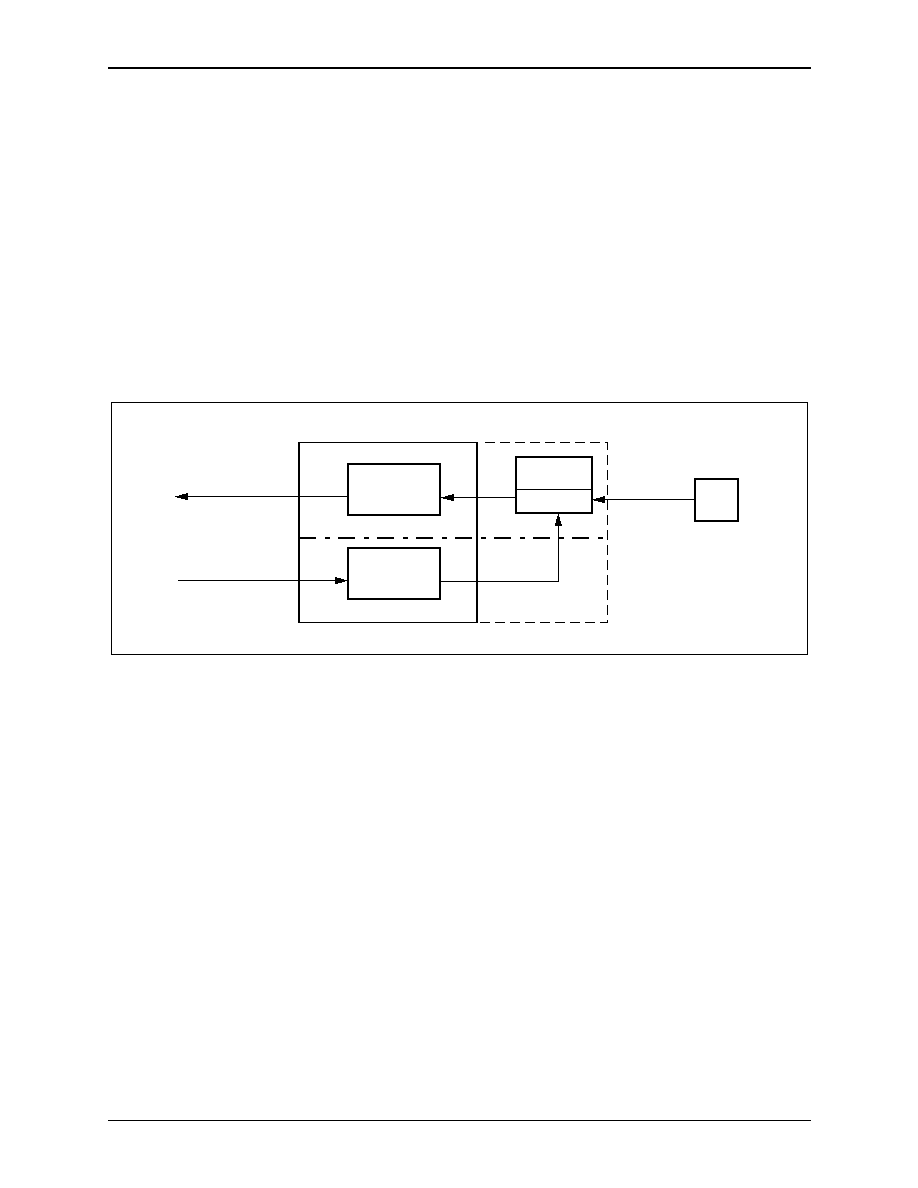
6.0 Traffic Management
RS8234
6.3 ABR Flow Control Manager
ATM ServiceSAR Plus with xBR Traffic Management
6-24
Mindspeed Technologies
TM
28234-DSH-001-B
6.3.2.2 Destination
Behavior
The RS8234 also responds to an incoming ABR cell stream as an ABR
Destination. The reassembly coprocessor processes received Forward RM cells. It
turns around this incoming information to the segmentation coprocessor via the
SCH_STATE part of the segmentation VCC Table entry. The segmentation
coprocessor then formats Backward RM cells containing this information and
inserts these turnaround RM cells into the transmit cell stream.
The RS8234 also provides a mechanism for the Destination host to apply
backpressure to the Source. The host notifies the RS8234 of internal system
congestion. The RS8234 passes this information to the Source via Backward RM
cells, to flow control the transmitting Source. The SAR also processes the EFCI
bit in the data cell header(s) per the rules in TM 4.1.
This process is illustrated in
Figure 6-14
.
6.3.2.3 Out-of-Rate
Cells
In addition to in-rate cell streams, the RS8234 can also generate out-of-rate
(CLP=1) cell streams. These CLP=1 streams compliment and enhance the
information flow contained in the in-rate cell streams. An example of the use of
this mechanism would be to send out-of-rate Forward RM cells on a channel if the
transmit rate on that channel has dropped below the schedule table minimum rate.
This provides a mechanism to restart scheduling of an ABR VCC whose rate has
dropped to zero or below the schedule table minimum rate.
6.3.3 Source and Destination Behaviors
ABR's Source and Destination Behavior Definitions are each listed in the ATM
Forum's TM 4.1 Specification. Refer to this specification for these definitions.
6.3.4 ABR VCC Parameters
The state of each VCC is stored individually in its SEG VCC Table entry. The
ABR parameters are stored in the SCH_STATE portion of the segmentation VCC
Table entry. Due to the large number of ABR parameters, the SCH_STATE of
ABR VCCs requires an additional location in the SEG VCC Table.
Figure 6-14. RS8234 ABR-ER Feedback Generation (Destination Behavior)
Segmentation
Coprocessor
Seg VCC
Table Entry
SCH_STATE
Reassembly
Coprocessor
BACKWARD_RM
FORWARD_RM
(Backward RM Cell Formatting)
(Forward RM Cell Processing)
Turnaround
Information
Congestion
Backpressure
Host
100074_053

RS8234
6.0 Traffic Management
ATM ServiceSAR Plus with xBR Traffic Management
6.3 ABR Flow Control Manager
28234-DSH-001-B
Mindspeed Technologies
TM
6-25
6.3.5 ABR Templates
The ABR Templates reside in SAR shared memory in a region referred to as the
ABR Instruction Table. The ABR Instruction Table contains one or more
templates. Individual VCCs are assigned to a single template. Each template
supports a group of VCCs. The key parameters contained in and controlled by the
ABR Templates are: PCR, Initial Cell Rate (ICR), MCR, RIF, RDF, and Nrm.
The user has the choice of defining MCR and ICR from the ABR Templates
or from fields in the SCH_STATE portion of the SEG VCC Table entry for each
connection, thus giving either per-template or per-connection control of MCR and
ICR. This choice is globally set using the ADV_ABR_TEMPL bit in the
SEG_CTRL register.
These ABR Templates are furnished by Mindspeed, and are downloaded to the
RS8234 as a complete microcoded state machine.
Three components constitute a complete template: a Cell Decision Table, a
Rate Decision Table and an Exponent Table.
The RS8234 uses the Cell Decision Table to select a cell type for insertion into
the transmitted in-rate cell stream.
The Rate Decision Table maps ABR cell stream rates to logical states. Each
state includes several vectors to other states, corresponding to different rates.
When an event forces a rate decision, the RS8234 decides which vector to follow
based on network stimulus (CI/NI), ER decisions, or internal timer/counter
expirations (ADTF and Crm).
The Exponent Table contains parameters for a piece-wise linear mapping
function. This function maps a TM 4.1 floating point rate representation (in
particular, the RM cell Explicit Rate field) to a Rate Decision Table index. The
Exponent Table is indexed by the Explicit Rate exponent. This mapping function
normalizes the ER field rate to the CI/NI state-based rate decision. Once
normalized, a rate can be chosen based on the minimum of the two rates.
6.3.6 Cell Type Decisions
6.3.6.1 In-rate Cell
Streams
Since every ABR connection in a network is full duplex, the RS8234 is a Source
and a Destination for each VCC. The RS8234 multiplexes user data cells,
Forward RM cells, and Backward RM cells into the in-rate ABR cell stream.
TM 4.1 Source Behaviors specify rules for the in-rate cell stream.
Figure 6-15 shows the desired result of the specification. First, the Source
transmits one Forward RM cell. A Backward RM cell follows. Finally, the Source
sends Nrm user data cells. At steady state, this sequence would be repeated with a
Forward RM cell marking the beginning of each sequence.
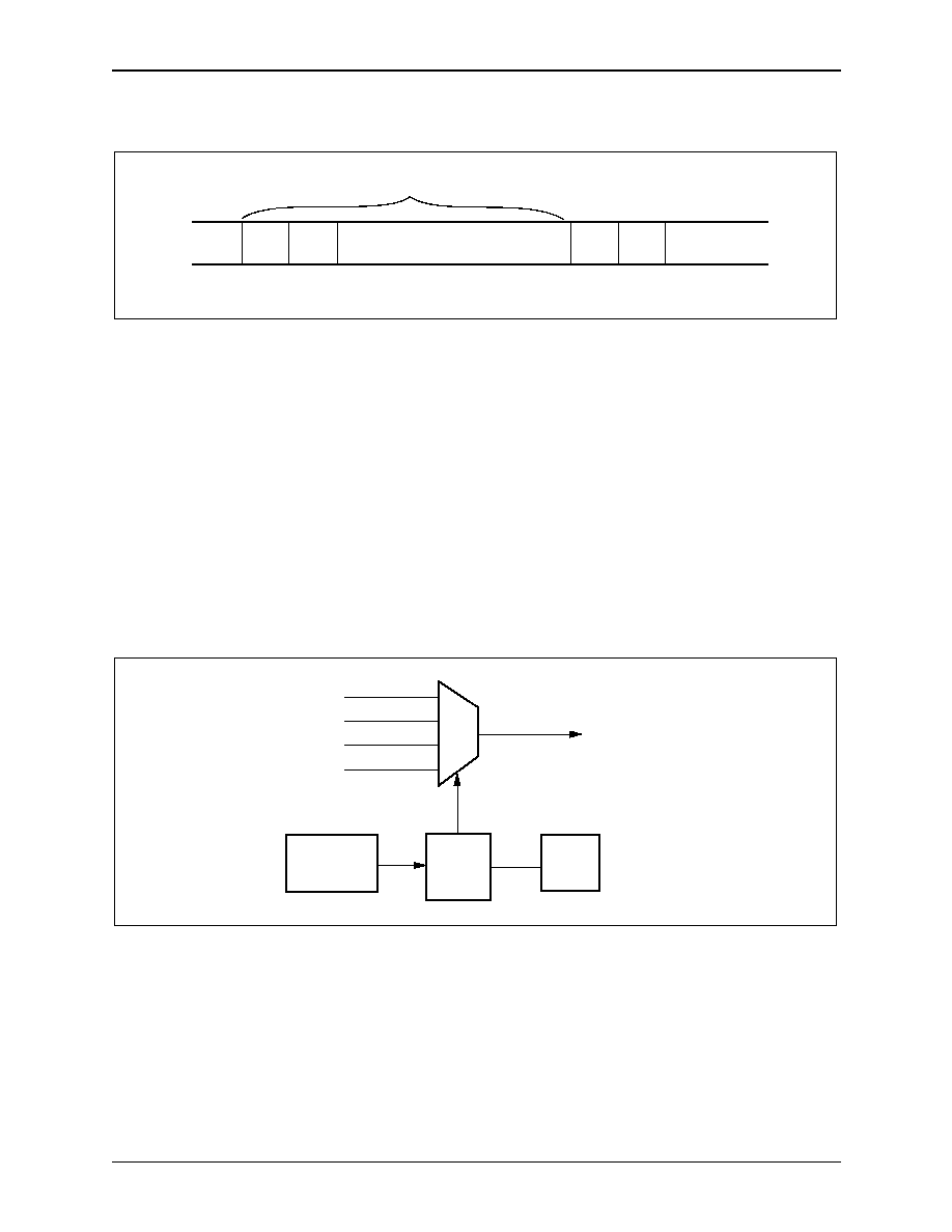
6.0 Traffic Management
RS8234
6.3 ABR Flow Control Manager
ATM ServiceSAR Plus with xBR Traffic Management
6-26
Mindspeed Technologies
TM
28234-DSH-001-B
Figure 6-15. Steady State ABR-ER Cell Stream
Unfortunately, due to the asynchronous, asymmetrical, and fluctuating
characteristics of ABR connections, all connections will not maintain a steady
state sequence. Furthermore, since it is an immature specification, the rules for
cell interleaving of in-rate cell streams may be modified slightly.
The RS8234 provides a programmable mechanism to comply with TM 4.1's
specification on cell stream interleaving. This Cell Type Decision algorithm
makes on-the-fly decisions concerning which type of cell to send, based on the
current state of the connection. Figure 6-16 shows a block diagram of the
algorithm. The ABR Flow Control Manager chooses a cell type based on a Cell
Decision Table and the VCC state. The segmentation coprocessor then formats
the appropriate cell type and sends it on the ABR in-rate cell stream. Note that the
ABR Flow Control Manager may choose to send no cell. This occurs when the
VCC has no user data to segment.
Figure 6-16. Cell Type Interleaving on ABR-ER Cell Stream
Since the Cell Decision Table template resides in SAR shared memory, the
user can modify it to optimize performance or react to changes in the ABR
specification. Furthermore, multiple tables allow groups of VCCs to be tuned for
different network policies.
BW_RM
FW_RM
FW_RM BW_RM
Nrm Data Cells
Note: Nominally, Nrm = 32
One FORWARD_RM Cell Period
100074_054
ABR-ER Cell Stream
Data Cell
Forward RM
Backward RM
Cell Type
Action
SEG VCC
State Table
(SCH_STATE)
Cell
Decision
Tab le
ABR
Flow
Control
Manager
None
100074_055
RS8234
6.0 Traffic Management
ATM ServiceSAR Plus with xBR Traffic Management
6.3 ABR Flow Control Manager
28234-DSH-001-B
Mindspeed Technologies
TM
6-27
6.3.6.2 ABR Cell
Decisions
The Cell Decision Tables reside in SAR shared memory as a segment of the Flow
Control Manager's ABR Instruction Table. Each entry of a table is an ABR Cell
Decision Block (ACDB). Each ACDB contains 16 Cell Type Actions. Cell Type
Actions result in one of four decisions: send in-rate Forward RM cell, send in-rate
Backward RM cell, send user data cell, or no action. A Cell Type Action is chosen
by a 4-bit ABR Cell Type Decision Vector (ACDV). The four bits of the ACDV
correspond to four current ABR VCC conditions.
Initialization Instructions
At system initialization, the Host loads one of more Cell Decision Tables into
SAR shared memory. Mindspeed provides standard Cell Decision Tables. The
system designer either uses these, or customized templates.
To assign an ABR VCC to a table, the Host initializes two SCH_STATE fields
at connection setup time. The first field, CELL_INDEX, tracks the current
ACDB position of the VCC. Source Behavior #2 specifies that the first in-rate
cell on a VCC is a Forward RM cell. Therefore, CELL_INDEX should be
initialized to an ACDB position which always decides to send a Forward RM cell.
The second field, FWD_INDEX, provides a reset point for the in-rate cell stream
sequence. Whenever the RS8234 transmits an in-rate Forward RM cell, it copies
FWD_INDEX to CELL_INDEX.
Run-time Operation
Each time an ABR cell transmit opportunity arises, the RS8234 makes a cell
decision. The SAR retrieves CELL_INDEX from SCH_STATE and chooses a
Cell Type Action location within the current ACDB. Table 6-4 shows the four
conditions which are used to form this vector. The presence of a condition sets the
vector bit to a one.
The SAR updates the CELL_INDEX field after each cell decision is made. If
an in-rate Forward RM cell is transmitted, FWD_INDEX is copied to
CELL_INDEX; otherwise, CELL_INDEX is incremented by one
(CELL_INDEX++). Therefore, the number of blocks in a Decision Table is
bounded by the maximum number of cell decisions made between transmitted
Forward RM cells, typically Nrm.
Table 6-4. ABR Cell Type Decision Vector (ACDV)
Bit
Name
Description
3
TRM_EXP
Time since last forward RM transmitted >= TRM
2
TA_PND
TA_PND bit set in VCC Table entry
1
TA_XMIT
TA_XMIT bit set in VCCTable entry
0
RUN
RUN bit set in VCC Table entry
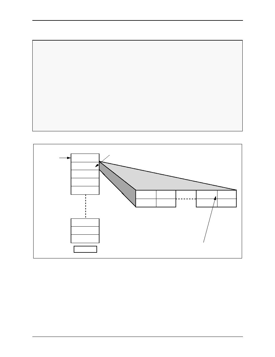
6.0 Traffic Management
RS8234
6.3 ABR Flow Control Manager
ATM ServiceSAR Plus with xBR Traffic Management
6-28
Mindspeed Technologies
TM
28234-DSH-001-B
Figure 6-17. Cell Decision Table for Nrm = 32
APPLICATION EXAMPLE: Cell Decision Table for Nrm=32
The Figure below, shows a typical Cell Decision Table. The anchor of the table, the FWD_INDEX
ACDB, is located at index 100 of the ABR Decision Table. Whenever a Forward RM cell is sent, this
ARCB will serve as the "reset" point for the decision state machine. When CELL_INDEX =
FWD_INDEX, a steady state ABR channel will transmit a Backward RM cell and advance the
CELL_INDEX. The diagram shows the next ACDB (101) in more detail. It contains the 16 Cell Type
Actions (BRM = Send Backward RM etc.). At the next cell transmission opportunity, the ABR Flow
Control Manager state machine will select a cell type by indexing into the ACDB according to the
ACDV. In this case, the only condition present is RUN=1, so ACDV = 0001b. Cell Type Action Index
1 is selected. For this ACDB, Cell Type Action 1 is DATA or "Send Data Cell". Therefore, the RS8234
will transmit a user data cell.
In steady state, CELL_INDEX will be incremented until it reaches ACDB 131. This ACDB
transmits a Forward RM Cell under all circumstances. Therefore, the RS8234 resets the CELL_INDEX
for this VCC to FWD_INDEX = 100, when it reaches this ACDB.
In this example, the Host should initialize CELL_INDEX to 131. The RS8234 would transmit a
Forward RM cell, and the sequence would continue from the FWD_INDEX.
100
101
102
103
104
129
130
131
Nrm = 32
7-BRM
6-BRM
1-DATA
0-NONE
15-FRM
14-FRM
9-FRM
8-FRM
CELL_INDEX(++)
ABR CELL DECISION BLOCK
FWD_INDEX
ABR Cell Type Decision Vector (ACDV)
[TRM_EXP, TA_PND, TA_XMIT, RUN] = 0001b
100074_056

RS8234
6.0 Traffic Management
ATM ServiceSAR Plus with xBR Traffic Management
6.3 ABR Flow Control Manager
28234-DSH-001-B
Mindspeed Technologies
TM
6-29
6.3.7 Rate Decisions and Updates
6.3.7.1 ABR Traffic
Shaping
The RS8234 schedules ABR VCCs as a single leaky bucket GCRA channel, but
the rate is subject to continual adjustment. At initialization, the Host assigns flow
controlled VCCs I and L parameters corresponding to the negotiated ICR. The
Cell Scheduler rate-shapes the initial traffic according to these GCRA
parameters. This shaped cell stream includes in-rate Forward and Backward RM
cells.
When feedback from the network results in flow control rate adjustments, the
ABR Flow Control Manager overwrites the I and L parameters in the
SCH_STATE of the VCC. The updated rates fall within the range of MCR and
PCR, which are specified on a per-connection basis.
6.3.7.2 Rate Adjustment
Overview
The RS8234 dynamically adjusts the rate of transmission for ABR VCCs based
upon network feedback, individual VCC parameters, and the current transmission
rate. The ABR Flow Control Manager uses all of these inputs to calculate the
ACR of the connection. This ACR corresponds to I and L GCRA parameters. The
RS8234 updates the I and L parameters of the VCC with the new ACR I and L
values.
The Flow Control Manager updates the transmission rate in response to two
types of events--the reception of a Backward RM cell or the transmission of a
Forward RM cell. The decision process is unique for each event type.
NOTE:
Note that both of these event types may occur in one cell slot. In this case,
the RS8234 makes both decisions before updating ACR.
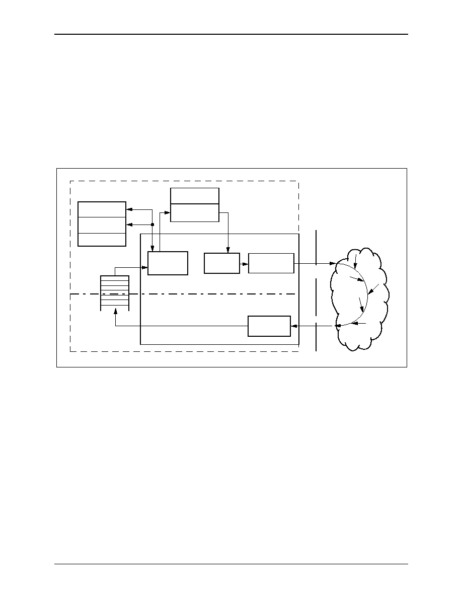
6.0 Traffic Management
RS8234
6.3 ABR Flow Control Manager
ATM ServiceSAR Plus with xBR Traffic Management
6-30
Mindspeed Technologies
TM
28234-DSH-001-B
6.3.7.3 Backward RM
Cell Flow Control
The ABR Rate Decision Table consists of many indexed entries. Each of these
entries is called an ABR Rate Decision Block or ARDB. Each ARDB represents a
possible transmission rate for an ABR VCC. The rate of an ARDB is a
monotonically increasing function of the index of the block.
The RS8234 tracks the state of each ABR connection's transmission rate by
storing its current ARDB index in the RATE_INDEX field of the SCH_STATE
VCC structure. This RATE_INDEX uniquely identifies the current transmission
rate of the VCC. Figure 6-18 illustrates a block diagram of Backward RM flow
control.
Figure 6-18. Backward_RM Flow Control, Block Diagram
Backward RM cells deliver stimulus for two flow control algorithms. The first
algorithm adjusts the state of a connection by a relative rate (RR) algorithm, in
response to the CI and NI bits. The second algorithm allows the network to
explicitly request a transmission rate in the ER RM cell field. Each of these
algorithms produces a candidate rate. The Source must adjust its rate to be less
than or equal to the lesser of these two candidates.
The RS8234 computes both rate candidates by first mapping all rate
parameters into rate index space. Since rate indexes are a monotonically
increasing function of rate, the RS8234 selects the candidate with the lowest rate
index.
For the RR algorithm, the conversion is embedded in the ARDBs themselves.
This algorithm can adjust the rate relative to the current rate. The adjusted rate
relates to the current rate by a constant multiplicative decrease or additive
increase. Specifically, the adjusted rate increases by RIF*PCR or decreases by
RDF*ACR. These values are pre-calculated and used to formulate a RS8234
ABR Rate Instruction Table, avoiding real time math.
BACKWARD_RM
ABR Decision
ABR Exponent
Table
ABR Rate
Instruction Table
ABR
Flow Control
Manager
Segmentation
Coprocessor
Rate
Decision
SAR
UNI
ATM
Network +
Destination
RSM/SEG
Queue
ABR
Cell Stream
SEG VCC
Table Entry
SCH_STATE
(RATE_INDEX)
Templates
Cell
Scheduler
Reassembly
Coprocessor
(CI, NI & ER Fields)
100074_057

RS8234
6.0 Traffic Management
ATM ServiceSAR Plus with xBR Traffic Management
6.3 ABR Flow Control Manager
28234-DSH-001-B
Mindspeed Technologies
TM
6-31
Each ARDB contains vectors to eight other ARDBs. Four of these vectors are
responses to the relative rate elements in Backward RM cells. The RS8234 uses
the CI/NI bits to choose an ARDB candidate from one of these four vectors. For
instance, if CI is set, the VCC must reduce its ACR by ACR*RDF. The vectors in
the ARDB that is chosen when CI is set point to ARDBs whose corresponding
rates are less than ACR-(ACR*RDF). The RS8234 recognizes the ARDB
indicated by the chosen vector, as the RR rate index candidate.
Figure 6-19. Relative Rate (RR) RATE_INDEX Candidate Selection
The RS8234 calculates the ER candidate by mapping the ER field from the
Backward RM cell into rate index space. This mapping converts the floating point
ER field rate representation to an absolute rate index. Note that this mapping does
not depend on the current rate of the connection. The RS8234 maps ER field to
rate indexes with a programmable piece-wise linear function. Each piece-wise
linear segment is described in the ABR Exponent Table. Again, the system
designer pre-calculates this mapping function to eliminate real-time floating point
math.
CONNECTION STATE (RATE_INDEX)
ACR
ACR - (ACR*RDF)
RR
INDEX
CANDIDATE
CI
(COMPLIANT
RELATIVE
RATES)
RR
�
ACR-(ACR*RDF)
ACR*RDF
RA
TE
100074_058

6.0 Traffic Management
RS8234
6.3 ABR Flow Control Manager
ATM ServiceSAR Plus with xBR Traffic Management
6-32
Mindspeed Technologies
TM
28234-DSH-001-B
Figure 6-20. Explicit Rate (ER) RATE_INDEX Candidate Selection
Once both candidates are identified, the RS8234 selects the smaller of the two,
each of which are
MCR. The winning candidate then replaces the current
RATE_INDEX in the VCC's SCH_STATE entry. Then the RS8234 uses this
RATE_INDEX to point to the corresponding appropriate RDB and, as specified
in TM 4.1, updates the VCC's rate parameter with the RDB's I and L parameters.
Figure 6-21 shows a block diagram of this process. The reassembly
coprocessor passes the CI, NI, and ER fields from the RM cell to the ABR Flow
Control Manager via the RSM/SEG Queue. The Flow Control Manager uses the
ABR Rate Decision Table and the Exponent Table, both programmable
components of an ER template, to calculate the two RATE_INDEX candidates,
each of which are
MCR. The min() function is applied to select a winning
candidate. Then the RS8234 updates the VCC's rate parameters with the newly
selected rate index. This rate index points to a Rate Decision Block whose I and L
parameters establish the new rate. The Cell Scheduler uses the updated rate to
schedule all future traffic (until the next rate update, of course.)
ER
ER
INDEX
CANDIDATE
RA
TE
CONNECTION STATE (RATE_INDEX)
100074_059
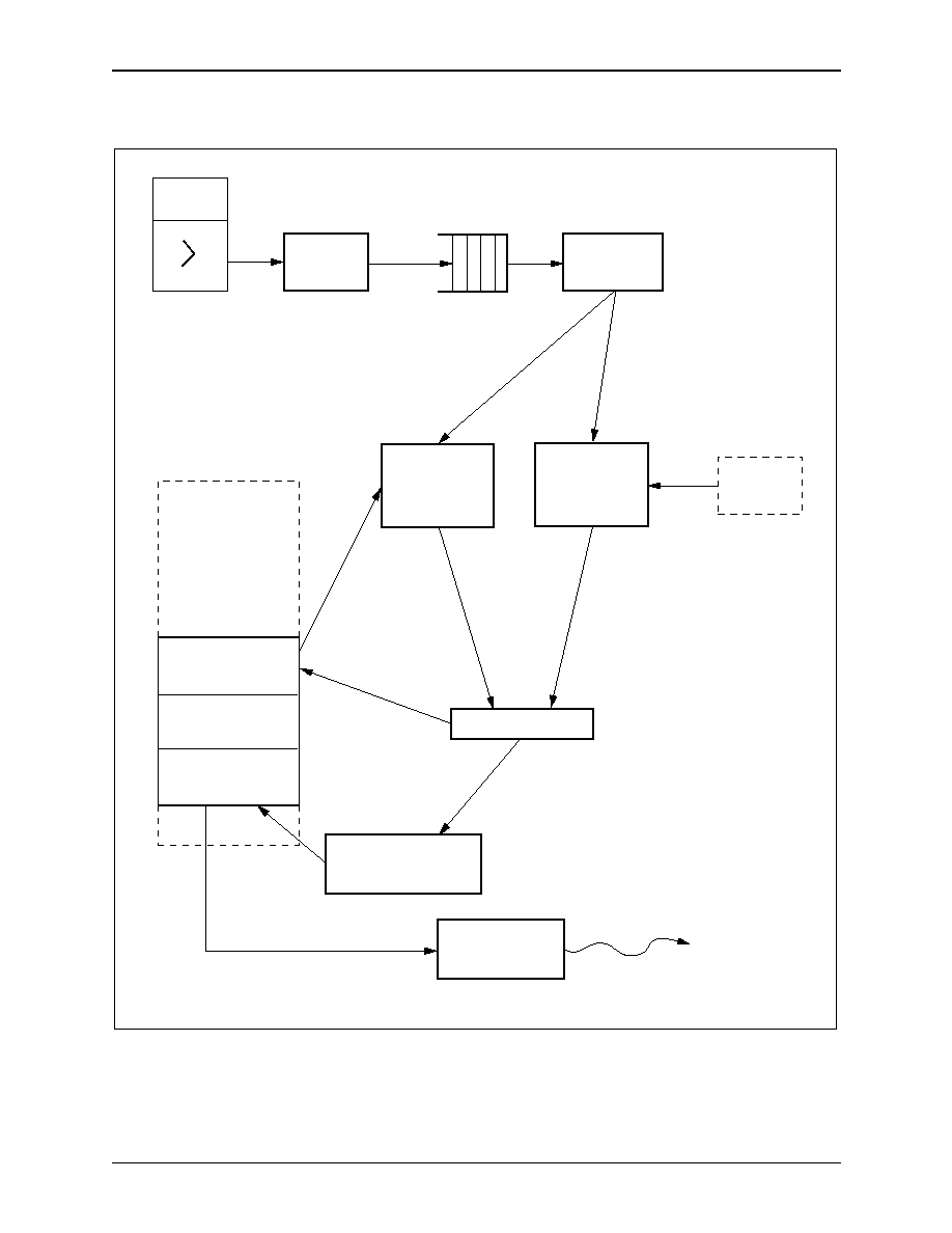
RS8234
6.0 Traffic Management
ATM ServiceSAR Plus with xBR Traffic Management
6.3 ABR Flow Control Manager
28234-DSH-001-B
Mindspeed Technologies
TM
6-33
Figure 6-21. Dynamic Traffic Shaping from RM Cell Feedback
Backward_
RM Cell
NI
CI
ER
Reassembly
Coprocessor
RSM/SEG
Queue
ABR Traffic
Manager
Segmentation VCC
Ta b le
Rate Decision
Vector Table
Traversal
Piece-Wise
Linear Mapping
Function
Exponent
Ta b le
Dynamic
Scheduler
TM4.0 ABR
Rate-Shaped
Traffic
RATE_INDEX
RR RATE_INDEX
ER RATE_INDEX
Min( )
RATE_INDEX -> NEW RATE
CURRENT RATE
Update
Update
VCC, ER,
CI, NI
CI, NI
ER
RR
SCH_STATE
Rate Decision Block
I & L parameters
100074_060
NOTE(S):
The RR RATE_INDEX and ER RATE_INDEX results are implicitly > or = MCR.

6.0 Traffic Management
RS8234
6.3 ABR Flow Control Manager
ATM ServiceSAR Plus with xBR Traffic Management
6-34
Mindspeed Technologies
TM
28234-DSH-001-B
6.3.7.4 Forward RM Cell
Transmission Decisions
The RS8234 also adjusts the transmission rates of an ABR in-rate cell stream
before sending a Forward RM cell. This adjustment utilizes a Rate Decision
Vector selection process. As stated above, four of the eight ARDB vectors are
used for CI/NI rate adjustment. The other four are used for Forward RM cell rate
adjustments.
Instead of the CI/NI bits, the Forward RM cell vector selection is based upon
the ADTF timer and the Crm counter. These internal measures may force the
connection to decrease its rate when sending an RM cell.
The ER for Forward RM cells on any channel is set in word 18 of the VCC
table entry (FWD_ER). The normal value for FWD_ER is PCR. When this field
is initialized in the VCC Table entry, it should be set to the rate specified by the
exponent table entries so that the resulting selected rate is
PCR. This is because
when a Forward RM cell is eventually received as a Backward RM cell, the
RS8234 will map the available cell rate (ACR) to a rate specified by the exponent
table. If PCR falls between two exponent table rates and FWD_ER is set to PCR,
the ACR of the connection will be limited to the lower of the two exponent table
rates, thereby lowering the rate below PCR.
6.3.7.5 Optional Rate
Adjustment in
Turnaround RM Cells
Based on Congestion in
the Switch
The system designer has the option of dictating a lowered explicit rate in
Turnaround RM cells, on any VCC which encounters congestion in the free buffer
queue for that VCC.
The Schedule Congestion register, SCH_CNG, includes a 32-bit field,
FBQ_CNG[31:0]; one bit for each of the 32 free buffer queues. The Host sets the
appropriate bit in this register field for any free buffer queue experiencing
congestion (i.e., an Empty condition).
The system designer can map each VCC to its free buffer queue ID by setting
the CONG_ID field in the VCC's SCH_STATE to the value of that FBQ ID.
NOTE:
This is a suggested mapping only. The system designer may wish to
employ some other mapping strategy than the above.
The designer enables this option for any rate by setting the CONG_ENA bit in
that rate's ABR Rate Decision Block (ARDB) to one. As a general rule, the
designer would set the CONG_ENA bit in those ARDBs describing higher rates,
when switch congestion is more likely to occur.
In each of the ARDBs that have the CONG_ENA bit set, the designer also
assigns a new lower explicit rate for congestion condition, and stores this rate in
the CONG_ER field of the ARDB.
During operation, when a Forward RM cell is received and CONG_ENA=1
for that rate, the RS8234 uses the CONG_ID value to look at the corresponding
SCH_CNG(FBQ_CNG[31:0]) bit to determine if it is set to logic high. If it is, the
RS8234 assigns the lowered rate in the CONG_ER field as the new explicit rate
in the Turnaround RM cell.

RS8234
6.0 Traffic Management
ATM ServiceSAR Plus with xBR Traffic Management
6.3 ABR Flow Control Manager
28234-DSH-001-B
Mindspeed Technologies
TM
6-35
6.3.7.6 Optional Rate
Adjustment Due to
Use-It-Or-Lose-It
Behavior
The Use-It-Or-Lose-It behavior defined in TM 4.1 describes a rate adjustment for
a VCC that has a high ACR but is not actually using that bandwidth in
transmission. In this case, the ACR is lowered to the level of ICR for that channel.
The RS8234's implementation of the TM 4.1 Use-It-Or-Lose-It behavior
allows the system designer to exactly tailor its operation. It uses a simple timeout
mechanism, dictatable for each explicit rate.
The designer selectively enables this function for the rate(s) he chooses by
setting the ACR_ENA bit to a logic high in each of the corresponding ABR Rate
Decision Blocks. As a general guideline, this bit would only be set in those
ARDBs dictating rates above ICR.
In those ARDBs which have this function enabled, the designer also specifies
two other values: ACR_TO (the trigger time for the timeout value when the rate
adjustment function activates), and ACR_INDEX (the new lower explicit rate
index to be established when the use-it-or-lose-it behavior is triggered).
As a general guideline, ACR_TO should be patterned on the ACR Decrease
Time Factor (ATDF), and ACR_INDEX should be patterned on the rate index for
ICR.
During run time on those ARDBs with the ACR_ENA bit set, the RS8234
compares RM_TIME (the schedule slot count at the time the last Forward RM
cell was generated) with ACR_TO. If the trigger point for the timeout has been
reached, the RS8234 generates a new Forward RM cell with the ACR_INDEX
value as the assigned new explicit rate.
6.3.8 Boundary Conditions and Out-of-Rate RM Cells
6.3.8.1 Calculated Rate
Boundaries
When the system designer pre-calculates the rates for the ARDB tables, the
designer must tailor those rates to fall within the two obvious upper and lower rate
boundaries--the lower rate boundary should not fall below MCR, and the upper
rate boundary should not be calculated above PCR.
6.3.8.2 Out-of-Rate
Forward RM Cell
Generation
A mechanism must exist to restart scheduling of a VCC once the rate on that
channel has dropped to zero, or is below the schedule table minimum rate (i.e.,
the rate is less than one schedule slot on the schedule table). Out-of-rate Forward
RM cell generation provides this mechanism.
To globally enable out-of-rate Forward RM cell generation, set
SCH_ABRBASE(OOR_ENA) to a logic high.
The system designer can set the SET_OOR bit to a logic high in any ABR
Rate Decision Block (ARDB). This enables out-of-rate Forward RM cell
generation for that rate.
When the actual cell rate on a channel has lowered to the point where
scheduling of the VCC has halted, and SET_OOR at that rate = 1, the RS8234
sets the SCH_OOR bit in the VCC's SCH_STATE to a logic high. The RS8234
will then generate an out-of-rate Forward RM cell on that channel.
The RS8234 calculates the rate for generation of out-of-rate Forward RM cells
as follows:
R = (maximum scheduled rate) = sysclk/SLOT_PER
generated rate = R / (OOR_INT + 1) / (VCC_MAX/2 + 1)
6.3.8.3 Out-of-Rate
Backward RM Cells
The system designer can set the TA_OOR bit to a logic high in any ABR Rate
Decision Block. This enables the RS8234 sending a Backward RM cell
out-of-rate when there is a pending Turnaround RM cell scheduled at that rate but
not yet sent, and another Forward RM cell is received.

6.0 Traffic Management
RS8234
6.4 GFC Flow Control Manager
ATM ServiceSAR Plus with xBR Traffic Management
6-36
Mindspeed Technologies
TM
28234-DSH-001-B
6.4 GFC Flow Control Manager
6.4.1 A Brief Overview of GFC
Generic Flow Control (GFC) is a one-way control mechanism which allows the
network equipment to control the input from an end station, for the class(es) of
traffic defined as controlled. This mechanism does not allow the end station to
exert any control on traffic from the network.
The usefulness of GFC is that it allows overbooking of the bandwidth on the
input side of the network switch buffers. This allows a much higher degree of
multiplexing than is otherwise possible, and allows the network-side costs of
connections to be significantly reduced. By overbooking the input bandwidth, a
high degree of sharing is possible and the buffer system can be used by more end
nodes than full bandwidth input would allow. GFC is used to coordinate access to
that bandwidth when temporary conflicts occur.
GFC provides a link-level, short-term, XON/XOFF-type flow control
mechanism that only works on the link from the end station to the first piece of
network equipment. The GFC protocols are defined and described in ITU
Recommendation I.361.
6.4.2 The RS8234's Implementation of GFC
The RS8234 implements the GFC one-queue mode. The reassembly coprocessor
provides Auto Configure and Command Detection. The segmentation
coprocessor provides Halt Processing and Per-transmit Queue SET_A control. It
does not implement the optional Queue B.
Once the link has been configured for GFC operation (as described in the
sub-section below), a received HALT indication will cause the segmentation
coprocessor to halt processing of all channels, both controlled and uncontrolled.
This halt condition will continue until a cell is received without the HALT
indication.
A received SET_A indication will increment the GFC credit counter by one. A
GFC controlled cell can be sent only when the GFC credit counter is equal to one.
Transmission of a GFC controlled cell decrements the credit counter by one. Each
of the eight transmit priority queues can be configured for GFC control by setting
the appropriate GFCn bit(s) in the Scheduling Priority (SCH_PRI) register. In this
way the SAR can segment both GFC controlled and GFC uncontrolled traffic
simultaneously. GFC controlled queues will be active only when the GFC credit
counter is equal to one.
CBR traffic is not affected by the SET_A command since it is not mapped into
a transmit priority queue. In addition, the segmentation coprocessor implements a
credit borrow algorithm that provides better utilization of the line when receive
and transmit cell streams are not synchronized. Up to one credit can be borrowed.
The user must control the transmitted GFC field via the HEADER_MOD and
GFC_DATA fields in the buffer descriptor entries. For GFC controlled channels,
GFC_DATA =
0101
; and for non-GFC controlled channels, GFC_DATA =
0001
.

RS8234
6.0 Traffic Management
ATM ServiceSAR Plus with xBR Traffic Management
6.4 GFC Flow Control Manager
28234-DSH-001-B
Mindspeed Technologies
TM
6-37
6.4.2.1 Configuring the
Link for GFC Operation
The following describes an example sequence of how to auto-configure a link for
GFC operation after the link has been initialized:
1.
Host sets a software GFC initialization timer = 0.
2.
Disable reassembly coprocessor by setting RSM_CTRL0(RSM_EN) = 0.
3.
Set the framer chip to pass unassigned cells.
4.
Enable the GFC link interrupt (GFC_LINK), by setting HOST_IMASK0
(EN_GFC_LINK) = 1.
5.
Read HOST_ISTAT0 register twice to clear it.
6.
Enable the reassembly coprocessor and set the GFC initialization timer to
some user-assigned value.
7.
Upon occurrence of an interrupt and before the GFC initialization timer
expires, read HOST_ISTAT0. If GFC_LINK is a logic high, continue. If
the timer expires before GFC_LINK is detected, do not enable the link for
GFC processing.
8.
Set SEG_CTRL(SEG_GFC) to a logic high.
9.
Set the GFCn bit(s) in the SCH_PRI register to enable the appropriate
priority queue(s) for GFC controlled operation.
10.
Set the framer chip to generate unassigned cells with GFC field in cell
headers set to the value of
0001
.
6.0 Traffic Management
RS8234
6.5 Traffic Management Control and Status Structures
ATM ServiceSAR Plus with xBR Traffic Management
6-38
Mindspeed Technologies
TM
28234-DSH-001-B
6.5 Traffic Management Control and Status
Structures
6.5.1 Schedule Table
At initialization, all words in the entire Schedule Table space should be written to
0xFFFFFFFF. Individual schedule slot entries can then be initialized as either
CBR slots or Tunnel slots as needed. The two formats are displayed in
Table 6-5
.
6.5.2 CBR-Specific Structures
6.5.2.1 CBR Traffic
A schedule slot is dedicated to a CBR connection by formatting the CBR bit to a
logic high and the CBR_TUN_ID field in the slot entry as illustrated in
Table 6-6
.
6.5.2.2 Tunnel Traffic
A schedule slot is dedicated to a CBR tunnel by formatting the CBR bit to a logic
low and the CBR_TUN_ID field of the slot entry as illustrated in
Table 6-7
. The
Schedule Slot field descriptions are detailed in
Table 6-8
.
Table 6-5. Schedule Slot Entry -- CBR/Tunnel Traffic
Word
31 30 29 28 27 26 25 24 23 22 21 20 19 18 17 16 15 14 13 12 11 10 9 8 7 6 5 4 3 2 1 0
0
CB
R
CBR_TUN_ID
(Reserved for 1 VBR/ABR pointer)
1-7
(1)(2)
(Reserved for 2 16-bit VBR/ABR pointers)
NOTE(S):
(1)
Word one is present only when the DBL_SLOT field in SEG_CTRL is set and USE_SCH_CTRL is not asserted, meaning two
words per schedule slot.
(2)
When USE_SCH_CTRL is asserted, the value of SLOT_DEPTH determines how many additional words are used in each
schedule slot; from 0 to 7 additional words.
Table 6-6. CBR_TUN_ID Field, Bit Definitions -- CBR Slot
Bit
31
30
29
28
27
26
25
24
23
22
21
20
19
18
17
16
Def.
1
CBR_VCC_INDEX (15 bits)
Table 6-7. CBR_TUN_ID Field, Bit Definitions -- Tunnel Slot
Bit
31
30
29
28
27
26
25
24
23
22
21
20
19
18
17
16
Def.
0
PRI3
PRI2
PRI1
PRI0
RS8234
6.0 Traffic Management
ATM ServiceSAR Plus with xBR Traffic Management
6.5 Traffic Management Control and Status Structures
28234-DSH-001-B
Mindspeed Technologies
TM
6-39
6.5.2.3 SCH_STATE
Fields For CBR
This section specifies the SCH_STATE portion (words 7�9) of the Segmentation
VCC Table entry, when SCH_MODE = CBR.
The CBR SCH_STATE is shown in
Table 6-9
, and the field descriptions are
detailed in
Table 6-10
.
Table 6-8. Schedule Slot Field Descriptions -- CBR Traffic
Field Name
Description
CBR
Set high to indicate a CBR slot; set low to indicate a tunnel slot.
PRI3
Specifies the highest priority of four possible scheduling priority queues to service when a scheduling
slot for this CBR tunnel becomes active.
PRI2
Specifies the second highest priority of four possible scheduling priority queues to service when a
scheduling slot for this CBR tunnel becomes active.
PRI1
Specifies the third highest priority of four possible scheduling priority queues to service when a
scheduling slot for this CBR tunnel becomes active.
PRI0
Specifies the lowest priority of four possible scheduling priority queues to service when a scheduling
slot for this CBR tunnel becomes active.
CBR_VCC_INDEX
Segmentation VCC Index for dedicated CBR schedule slot. CBR VCC indexes range from 0x0000 to
0x7FFE.
NOTE(S):
If the user wants only one priority of traffic scheduled in the CBR tunnel, then assign the priority level to PRI3 and make
PRI2 the same priority. PRI1 and PRI0 values are Don't Cares in this case. If two priorities are to be assigned to the tunnel, then
assign the higher priority to PRI3 and the lower priority to PRI2, making PRI1 the same as PRI2. PRI0 is a Don't Care in this
case. If three priorities are to be assigned to the tunnel, then assign the priorities by level to PRI3 (highest), PRI2 and PRI1
(lowest), making PRI0 the same as PRI1. Note that TUN_PRI0_OFFSET can be used to set PRI0 = PRI1, as needed.
Table 6-9. SCH_STATE for SCH_MODE = CBR
Word 31 30 29 28 27 26 25 24 23 22 21 20 19 18 17 16 15 14 13 12 11 10 9
8
7
6
5
4
3
2
1
0
7
Reserved
TUN_PRI_3
TUN_PRI_2
TUN_PRI_1
TUN_PRI
_0
8
Reserved
9
Reserved
6.0 Traffic Management
RS8234
6.5 Traffic Management Control and Status Structures
ATM ServiceSAR Plus with xBR Traffic Management
6-40
Mindspeed Technologies
TM
28234-DSH-001-B
6.5.3 VBR-Specific Structures
6.5.3.1 VBR SCH_STATE
Table 6-11
and
Table 6-12
the SCH_STATE part of the Segmentation VCC Table
entry, which consists of words 7�9 for VBR.
See
Section 6.2.4, VBR Traffic
, for key data on I and L values.
6.5.3.2 \VBR1 or VBR2
Schedule State Table
Table 6-10. CBR SCH_STATE Field Descriptions
Field Name
Description
TUN_PRI_3
When SCH_MODE is CBR and CBR_W_TUN bit is set to 1, this field specifies the highest priority of four
possible scheduling priority queues to service in place of the unused CBR slot. (This field is not active
when CBR_W_TUN = 0.)
TUN_PRI_2
When SCH_MODE is CBR and CBR_W_TUN bit is set to 1, this field specifies the second highest priority
of four possible scheduling priority queues to service in place of the unused CBR slot. (This field is not
active when CBR_W_TUN = 0.)
TUN_PRI_1
When SCH_MODE is CBR and CBR_W_TUN bit is set to 1, this field specifies the third highest priority of
four possible scheduling priority queues to service in place of the unused CBR slot. (This field is not
active when CBR_W_TUN = 0.)
TUN_PRI_0
When SCH_MODE is CBR and CBR_W_TUN bit is set to 1, this field specifies the lowest priority of four
possible scheduling priority queues to service in place of the unused CBR slot. (This field is not active
when CBR_W_TUN = 0.)
Table 6-11. SCH_STATE for SCH_MODE = VBR1 or VBR2
Word 31 30 29 28 27 26 25 24 23 22 21 20 19 18 17 16 15 14 13 12 11 10 9
8
7
6
5
4
3
2
1
0
7
BUCKET2
(MSB)
L1_EXP
L1_MAN
I1_EXP
I1_MAN
8
BUCKET2
(LSB)
Reserved
9
Reserved

RS8234
6.0 Traffic Management
ATM ServiceSAR Plus with xBR Traffic Management
6.5 Traffic Management Control and Status Structures
28234-DSH-001-B
Mindspeed Technologies
TM
6-41
6.5.3.3 VBR1 or VBR2
Schedule State Table
Table 6-12. VBR1 and VBR2 SCH_STATE Field Descriptions
Field Name
Description
BUCKET2
Index into Bucket table to give I2 and L2 for SCHED_MODE = VBR2 & VBRC. Bucket table base is given
by SEG_BCKB register field. Entries in Bucket table have same format as L1_EXP, L1_MAN, I1_EXP, and
I1_MAN.
L1_EXP
GCRA L parameter exponent for bucket 1.
L1_EXP must satisfy
L1_EXP <= min(I1_EXP + 9,29).
L1_EXP that does not satisfy
L1_EXP >= I1_EXP - 9
will have an effective L1 value of zero.
L1_MAN
GCRA L parameter mantissa for bucket 1.
Bucket 1 L value is:
2
(L1_EXP - 10)
(1+L1_MAN/512).
I1_EXP
GCRA I parameter exponent for bucket 1.
I1_EXP must satisfy
10 <= I1_EXP <= 25.
I1_MAN
GCRA I parameter mantissa for bucket 1.
Bucket 1 I value is:
2
(I1_EXP - 10)
(1+I1_MAN/512).
The GCRA I value is expressed in cell slot intervals. Example
(I is not expressed in cells/sec.)
I
1
PCR
------------
R
MAX
�
=
Table 6-13. SCH_STATE for SCH_MODE = VBR1 or VBR2
Word 31 30 29 28 27 26 25 24 23 22 21 20 19 18 17 16 15 14 13 12 11 10 9
8
7
6
5
4
3
2
1
0
7
BUCKET2
(MSB)
L1_EXP
L1_MAN
I1_EXP
I1_MAN
8
BUCKET2
(LSB)
PRESENT
9
DEL
T
A2
_
S
IGN
DEL
T
A2
_
N
Z
DEL
T
A1
_
S
IGN
DEL
T
A1
_
N
Z
DELTA2_EXP
DELTA2_MAN
DELTA1_EXP
DELTA1_MAN

6.0 Traffic Management
RS8234
6.5 Traffic Management Control and Status Structures
ATM ServiceSAR Plus with xBR Traffic Management
6-42
Mindspeed Technologies
TM
28234-DSH-001-B
DELTA1 and DELTA2 give the offsets to the desired position for each bucket and
need to have the same resolution as I and L.
6.5.3.4 Bucket Table for
VBR2 and VBRC
The Bucket Table has only 256 entries.
Table 6-15
and
Table 6-16
display the
entry format and field descriptions for the Bucket Table.
Table 6-14. VBR1 and VBR2 SCH_STATE Field Descriptions
Field Name
Description
BUCKET2
Index into Bucket table to give I2 and L2 for SCHED_MODE = VBR2 & VBRC. Bucket table base is
given by SEG_BCKB register field. Entries in Bucket table have same format as L1_EXP, L1_MAN,
I1_EXP, and I1_MAN.
L1_EXP
GCRA L parameter exponent for bucket 1.
L1_EXP must satisfy
L1_EXP <= min(I1_EXP + 9,29).
L1_EXP that does not satisfy
L1_EXP >= I1_EXP - 9
will have an effective L1 value of zero.
L1_MAN
GCRA L parameter mantissa for bucket 1.
Bucket 1 L value is:
2
(L1_EXP - 10)
(1+L1_MAN/512).
I1_EXP
GCRA I parameter exponent for bucket 1.
I1_EXP must satisfy
10 <= I1_EXP <= 25.
I1_MAN
GCRA I parameter mantissa for bucket 1.
Bucket 1 I value is:
2
(I1_EXP - 10)
(1+I1_MAN/512).
PRESENT
Current Schedule Table position.
DELTA2_SIGN
When set, indicates delta is negative for bucket 2.
DELTA2_NZ
When set, indicates delta is non-zero for bucket 2.
DELTA1_SIGN
When set, indicates delta is negative for bucket 1.
DELTA1_NZ
When set, indicates delta is non-zero for bucket 1.
DELTA2_EXP
Delta exponent for bucket 2.
DELTA2_MAN
Delta mantissa for bucket 2.
Desired position for bucket 2 is:
DELTA2_NZ * 2
(DELTA2_EXP - 10)
(1 + DELTA2_MAN/512) + PRESENT.
DELTA1_EXP
Delta exponent for bucket 1.
DELTA1_MAN
Delta mantissa for bucket 1.
Desired position for bucket 1 is:
DELTA1_NZ * 2
(DELTA1_EXP - 10)
(1 + DELTA1_MAN/512) + PRESENT.
NOTE(S):
The GCRA I value is expressed in cell slot intervals. Example
(I is not expressed in
cells/sec.)
I
1
PCR
------------
R
MAX
�
=
Table 6-15. Bucket Table Entry
Word 31 30 29 28 27 26 25 24 23 22 21 20 19 18 17 16 15 14 13 12 11 10 9
8
7
6
5
4
3
2
1
0
0
Rsvd
L2_EXP
L2_MAN
I2_EXP
I2_MAN

RS8234
6.0 Traffic Management
ATM ServiceSAR Plus with xBR Traffic Management
6.5 Traffic Management Control and Status Structures
28234-DSH-001-B
Mindspeed Technologies
TM
6-43
6.5.4 GFR-Specific Structures
6.5.4.1 GFR Schedule
State Table
Table 6-17
and
Table 6-18
detail the SCH_STATE structure for GFR traffic.
Table 6-16. Bucket Table Entry Field Descriptions
Field Name
Description
L2_EXP
GCRA L parameter exponent for bucket 2.
L2_EXP must satisfy
L2_EXP <= min(I2_EXP + 9,29).
L2_EXP that does not satisfy
L2_EXP >= I2_EX - 9
will have an effective L2 value of zero.
L2_MAN
GCRA L parameter mantissa for bucket 2.
Bucket 2 L value is:
2
(L2_EXP - 10)
(1+L2_MAN/512).
I2_EXP
GCRA I parameter exponent for bucket 2.
I2_EXP must satisfy
10 <= I2_EXP <= 25.
I2_MAN
GCRA I parameter mantissa for bucket 2.
Bucket 2 I value is:
2
(I2_EXP - 10)
(1+I2_MAN/512).
Table 6-17. SCH_STATE for SCH_MODE = GFR
Word 31 30 29 28 27 26 25 24 23 22 21 20 19 18 17 16 15 14 13 12 11 10 9
8
7
6
5
4
3
2
1
0
7
MCRLIM_IDX
(MSB)
L1_EXP
L1_MAN
I1_EXP
I1_MAN
8
MCRLIM_IDX
(LSB)
Reserved
9
Rsvd
Reserved
Reserved
Reserved
Table 6-18. SCH_STATE Field Descriptions for SCH_MODE = GFR
Field Name
Description
MCRLIM_IDX
Index into table of 256 MCR LIMIT values each specifying an increase in the VCC's priority by one if the
VCC's rate falls below MCR. The table base is located on top of the BUCKET2 table whose base is given
by SEG_BCKB register field. The BUCKET2 table is 1KB in length. Table values are in the form of a
non-zero bit, exponent, and mantissa such that MCR_LIMIT is:
MCR_LIM_NZ * 2
(MCR_LIM_EXP-10)
(1+MCR_LIM_MAN/512)
L1_EXP
GCRA L parameter exponent for MCR bucket.
L1_EXP must satisfy:
LI_EXP that does not satisfy
will have effective L1 value of zero.
L1_MAN
GCRA L parameter mantissa for MCR bucket
Bucket 1 L value is:
2
(L1_EXP - 10)
(1+L1_MAN/512)
I1_EXP
GCRA I parameter exponent for MCR bucket.
I1_EXP must satisfy
10 <= I2_EXP <= 25
I1_MAN
GCRA I parameter mantissa for MCR bucket.
Bucket 1 I value is:
2
(I1_EXP - 10)
(1+I1_MAN/512)
L1_EXP
min I1_EXP
9
+
29
(
,
)
L1_EXP
I1_EXP
9
�

6.0 Traffic Management
RS8234
6.5 Traffic Management Control and Status Structures
ATM ServiceSAR Plus with xBR Traffic Management
6-44
Mindspeed Technologies
TM
28234-DSH-001-B
6.5.4.2 GFR MCR Limit
Bucket Table
The 128 words of this table contain 256 MCR Limit values, two bucket table
entries per word. The table base is on top of the Bucket2 Table. Table values are in
the form of a non-zero bit, exponent and mantissa such that MCR_LIMIT is:
Table 6-19
and
Table 6-20
describe the MCR Limit Bucket Table.
MCR_LIM_NZ 2
MCR_LIM_EXP
10
�
(
)
1
MCR_LIM_MAN 512
/
+
(
)
Table 6-19. GFR MCR Limit Bucket Table Entry
Word 31 30 29 28 27 26 25 24 23 22 21 20 19 18 17 16 15 14 13 12 11 10 9
8
7
6
5
4
3
2
1
0
0
Rs
v
d
N
ONZ
ERO
MCR_EXP
MCR_MAN
Rs
v
d
N
ONZ
ERO
MCR_EXP
MCR_MAN
Table 6-20. GFR MCR Bucket Table Entry Field Descriptions
Field Name
Description
MCR_EXP
GFR MCR limit exponent.
MCR_EXP must satisfy
MCR_EXP <= 29.
MCR_MAN
GFR MCR limit mantissa.
MCR limit is:
NONZERO * 2
(MCR_EXP-10)
(1+MCR_MAN/512).
VCC priority will be increased by one when rate falls below 1/MCR limit.
NONZERO
GFR MCR limit is non-zero.

RS8234
6.0 Traffic Management
ATM ServiceSAR Plus with xBR Traffic Management
6.5 Traffic Management Control and Status Structures
28234-DSH-001-B
Mindspeed Technologies
TM
6-45
6.5.5 ABR-Specific Structures
6.5.5.1 ABR Schedule
State Table
Table 6-21
describes the SCH_STATE entries in the segmentation VCC Table
for the ABR service class.
Table 6-22
details the field descriptions for the ABR
SCH_STATE fields.
KEY:
= Values are furnished by the ABR Templates.
Table 6-21. SCH_STATE for SCH_MODE = ABR
Word 31 30 29 28 27 26 25 24 23 22 21 20 19 18 17 16 15 14 13 12 11 10 9
8
7
6
5
4
3
2
1
0
7
Rsvd
L_EXP
L_MAN
I_EXP
I_MAN
8
Rsvd
PRESENT
9
Rs
v
d
M
C
R_
LI
M
_
NZ
DEL
T
A
_
SI
GN
DE
L
T
A_
NZ
MCR_LIM_EXP
MCR_LIM_MAN
DELTA_EXP
DELTA_MAN
10
CONG_ID
OO
R_P
R
I
Rs
v
d
TM
_E
XP
BCK
_OO
R
F
W
D_
OOR
SCH
_OO
R
TA
_
X
M
I
T
TA
_
P
N
D
CELL_INDEX
11
FWD_INDEX
RM_TIME
12
RATE_INDEX
EB_INDEX
13
Rs
v
d
CRM
UNACK
14
Reserved
NEXT_OOR
15
MCR_INDEX
ICR_INDEX
16
1
TA_ID
TA
_
D
I
R
TA
_
B
N
TA
_
C
I
TA
_
N
I
TA
_
R
A
Rsvd
TA_ER
17
1
TA_CCR
TA_MCR
18
FWD_ID
FWD
_
D
I
R
FW
D
_
B
N
FWD
_
C
I
FWD
_
N
I
F
W
D_
RA
Rsvd
FWD_ER
19
Reserved
FWD_MCR
NOTE(S):
(1)
Words 16 and 17 are written directly by the RSm coprocessor (turnaround information).

6.0 Traffic Management
RS8234
6.5 Traffic Management Control and Status Structures
ATM ServiceSAR Plus with xBR Traffic Management
6-46
Mindspeed Technologies
TM
28234-DSH-001-B
Table 6-22. ABR SCH_STATE Field Descriptions (1 of 2)
Field Name
Description
L_EXP
GCRA L parameter exponent for ER rate.
L_MAN
GCRA L parameter mantissa for ER rate.
I_EXP
GCRA I parameter exponent for ER rate.
I_MAN
GCRA I parameter mantissa for ER rate.
PRESENT
Current schedule table position.
MCR_LIM_NZ
MCR Limit is non-zero.
To disable priority bumping, MCR_LIMIT must be set to its maximum value. Thus, MCR_LIM_NZ
must be set to 1.
DELTA_SIGN
Delta is negative for ER rate.
DELTA_NZ
Delta is non-zero for ER rate.
MCR_LIM_EXP
MCR Limit exponent.
MCR_LIM_EXP must satisfy
MCR_LIM_EXP <= 29.
To disable priority bumping, MCR_LIMIT must be set to its maximum value. Thus, MCR_LIM_EXP
must be set to a decimal value of 31 (i.e., binary all-ones).
MCR_LIM_MAN
MCR Limit mantissa.
MCR_LIMIT is:
MCR_LIM_NZ * 2
(MCR_LIM_EXP-10)
(1+MCR_LIM_MAN/512)
This format for calculating MCR_LIMIT is the same as used with the GCRA I parameter to calculate
rates.
VCC priority will be increased by one when rate falls below 1/MCR_LIM.
To disable priority bumping, MCR_LIMIT must be set to its maximum value. Thus, MCR_LIM_MAN
must be set to a decimal value of 511 (i.e., binary all-ones).
DELTA_EXP
Delta exponent for ER rate.
DELTA_MAN
Delta mantissa for ER rate.
Desired position for ER rate is:
DELTA_NZ * 2
(DELTA_EXP-10)
(1+DELTA_MAN/512)+PRESENT
CONG_ID
Congestion Index for changing ER on turnaround RM cells. The ER in the turnaround cell is changed
only if the FBQ_CNG[CONG_ID] bit is set in the SCH_CNG register. The normal setting for this field is
the free buffer queue ID for the VCC.
OOR_PRI
Segmentation priority for out-of-rate RM cells.
TM_EXP
RM_TIME value has expired and is no longer valid.
BCK_OOR
Backward RM cell has been scheduled out-of-rate.
FWD_OOR
Forward RM cell has been scheduled out-of-rate.
SCH_OOR
VCC has halted due to low ACR and has out-of-rate Forward RM cells enabled.
TA_XMIT
A Backward RM cell has been transmitted after the last Forward RM cell transmitted.
TA_PND
A Backward RM cell is waiting for transmission.
CELL_INDEX
ER cell type decision block index for cell type decisions. The cell type decision block is located at byte
address SCH_ABRB*128 + 8*CELL_INDEX.

RS8234
6.0 Traffic Management
ATM ServiceSAR Plus with xBR Traffic Management
6.5 Traffic Management Control and Status Structures
28234-DSH-001-B
Mindspeed Technologies
TM
6-47
FWD_INDEX
ER cell type decision block index for cell type decisions after a Forward RM cell is transmitted.
RM_TIME
Global slot count [21:6] at time of last Forward RM transmission.
RATE_INDEX
ER rate decision block index. The rate decision block is located at byte address SCH_ABRB*128 +
32*RATE_INDEX.
EB_INDEX
ER exponent table index for rate index block. The exponent table is located at byte address
SCH_ABRB*128 + EB_INDEX*128.
CRM
ER parameter.
UNACK
Number of Forward RM cells transmitted since last Backward RM cell received. Initialize to zero.
NEXT_OOR
Next VCC index for linking out-of-rate RM cells.
MCR_INDEX
Minimum Cell Rate decision block index. The rate decision block is located at byte address
SCH_ERB*128 + 32*MCR_INDEX.
ICR_INDEX
Initial Cell Rate decision block index. The rate decision block is locate at byte address SCH_ERB*128 +
32*ICR_INDEX.
TA_ID
ID field from most recent received Forward RM cell. This field is written by the SAR.
TA_DIR
DIR field for turnaround (Backward) RM cell. This field is written by the SAR.
TA_BN
BN field for turnaround (Backward) RM cell. This field is written by the SAR.
TA_CI
CI field for turnaround (Backward) RM cell. This field is written by the SAR.
TA_NI
NI field for turnaround (Backward) RM cell. This field is written by the SAR.
TA_RA
RA field from most recent received Forward RM cell. This field is written by the SAR.
TA_ER
ER field for turnaround (Backward) RM cell. This field is written by the SAR.
TA_CCR
CCR field from most recent received Forward RM cell. This field is written by the SAR.
TA_MCR
MCR field from most recent received Forward RM cell. This field is written by the SAR.
FWD_ID
ID field for transmitted Forward RM cells. This field is supplied by the user.
FWD_DIR
DIR field for transmitted Forward RM cells. This field is supplied by the user.
FWD_BN
BN field for transmitted Forward RM cells. This field is supplied by the user.
FWD_CI
CI field for transmitted Forward RM cells. This field is supplied by the user.
FWD_NI
NI field for transmitted Forward RM cells. This field is supplied by the user.
FWD_RA
RA field for transmitted Forward RM cells. This field is supplied by the user.
FWD_ER
ER field for transmitted Forward RM cells. This field is supplied by the user.
FWD_MCR
MCR field for transmitted Forward RM cells. This field is supplied by the user.
Table 6-22. ABR SCH_STATE Field Descriptions (2 of 2)
Field Name
Description
6.0 Traffic Management
RS8234
6.5 Traffic Management Control and Status Structures
ATM ServiceSAR Plus with xBR Traffic Management
6-48
Mindspeed Technologies
TM
28234-DSH-001-B
6.5.6 ABR Instruction Tables
An ABR cell decision block consists of 16 Cell Type Actions. The correct cell
type action is selected with a 4-bit cell type decision vector.
Table 6-23. ABR Cell Decision Block (ACDB)
Word 31 30 29 28 27 26 25 24 23 22 21 20 19 18 17 16 15 14 13 12 11 10 9
8
7
6
5
4
3
2
1
0
0
CT_ACT7
CT_ACT6
CT_ACT5
CT_ACT4
CT_ACT3
CT_ACT2
CT_ACT1
CT_ACT0
1
CT_ACT15
CT_ACT14
CT_ACT13
CT_ACT12
CT_ACT11
CT_ACT10
CT_ACT9
CT_ACT8
Table 6-24. ABR Cell Type Actions
Value
Description
0000
Reserved (no action).
0001
Send data cell without reporting I_MAN and I_EXP in status entry.
0010-1000
Reserved (no action).
1001
Send data cell with reporting of I_MAN and I_EXP in status entry.
1010
Send in-rate Forward RM cell.
1011
Send in-rate Backward RM cell.
1110-1111
Reserved (no action).
Table 6-25. ABR Cell Type Decision Vector (ACDV)
Bit
Name
Description
3
TRM_EXP
Time since last Forward RM transmitted >= TRM.
2
TA_PND
TA_PND bit set in VCC Table entry.
1
TA_XMIT
TA_XMIT bit set in VCC Table entry.
0
RUN
RUN bit set in VCC Table entry.

RS8234
6.0 Traffic Management
ATM ServiceSAR Plus with xBR Traffic Management
6.5 Traffic Management Control and Status Structures
28234-DSH-001-B
Mindspeed Technologies
TM
6-49
Table 6-26. ABR Rate Decision Block (ARDB)
Word 31 30 29 28 27 26 25 24 23 22 21 20 19 18 17 16 15 14 13 12 11 10 9
8
7
6
5
4
3
2
1
0
0
ACR_
EN
CONG
_
E
N
T
A
_
OOR
SET_
O
O
R
L_EXP
L_MAN
I_EXP
I_MAN
1
CONG_ER
ACR
2
ACR_INDEX
ACR_TO
3
Rsvd
4
NEW_RATE1
NEW_RATE0
5
NEW_RATE3
NEW_RATE2
6
NEW_RATE5
NEW_RATE4
7
NEW_RATE7
NEW_RATE6
Table 6-27. ARDB Field Descriptions
Field Name
Description
ACR_EN
ACR "Use-It-Or-Lose-It" behavior enabled on rate.
CONG_EN
Enable congestion rate adjustment on rate.
TA_OOR
Out of rate RM cell turnaround enabled on rate.
SET_OOR
Rate is below schedule table min rate. Enable out-of-rate Forward RM generation to restart VCC.
L_EXP
GCRA L parameter exponent for ER rate.
L_MAN
GCRA L parameter mantissa for ER rate.
I_EXP
GCRA I parameter exponent for ER rate.
I_MAN
GCRA I parameter mantissa for ER rate. I and L parameters are copied to VCC structure.
CONG_ER
New ER for congestion.
ACR
ACR field for transmitted forward RM cell.
ACR_INDEX
New rate index for ACR lose-it behavior triggered. The new rate decision block is located at byte
address SCH_ERB*128 + 32*ACR_INDEX.
ACR_TO
ACR Lose-it behavior trigger time.
NEW_RATE7 -
NEW_RATE0
New rate indexes. The correct new rate index is selected with a 3-bit rate decision vector. The rate
decision block is located at byte address SCH_ERB*128 + 32*NEW_RATEn.
6.0 Traffic Management
RS8234
6.5 Traffic Management Control and Status Structures
ATM ServiceSAR Plus with xBR Traffic Management
6-50
Mindspeed Technologies
TM
28234-DSH-001-B
An exponent table maps an explicit rate to a rate decision block index. The table is
indexed by the ER exponent.
Figure 6-22 illustrates the linkage pattern between the components of the ABR
Instruction Tables.
Table 6-28. ABR Rate Decision Vector (ARDV)
Value
Description
000
Reserved/Unused, or
Transmit Forward RM cell, ADTF not expired, CRM not expired
001
Transmit Forward RM cell, ADTF not expired, CRM expired
010
Reserved/Unused, or
Transmit Forward RM cell, ADTF expired, CRM not expired
011
Reserved/Unused, or
Transmit Forward RM cell, ADTF expired, CRM expired
100
Received Backward RM cell with CI = 0, NI = 0
101
Received Backward RM cell with CI = 0, NI = 1
110
Received Backward RM cell with CI = 1, NI = 0
111
Received Backward RM cell with CI = 1, NI = 1
Table 6-29. Exponent Table
Word 31 30 29 28 27 26 25 24 23 22 21 20 19 18 17 16 15 14 13 12 11 10 9
8
7
6
5
4
3
2
1
0
0
Rsvd
SHIFT0
EXP_BASE0
...
Rsvd
...
...
31
Rsvd
SHIFT31
EXP_BASE31
Table 6-30. Exponent Table Field Descriptions
Field Name
Description
EXP_BASE31-EXP_BA
SE0
Base rate decision block index.
SHIFT31-SHIFT0
Shift of ER mantissa. Rate index is EXP_BASEn + mantissa>>SHIFTn.
If the ER NZ bit is not set, the rate index is EXP_BASE0.
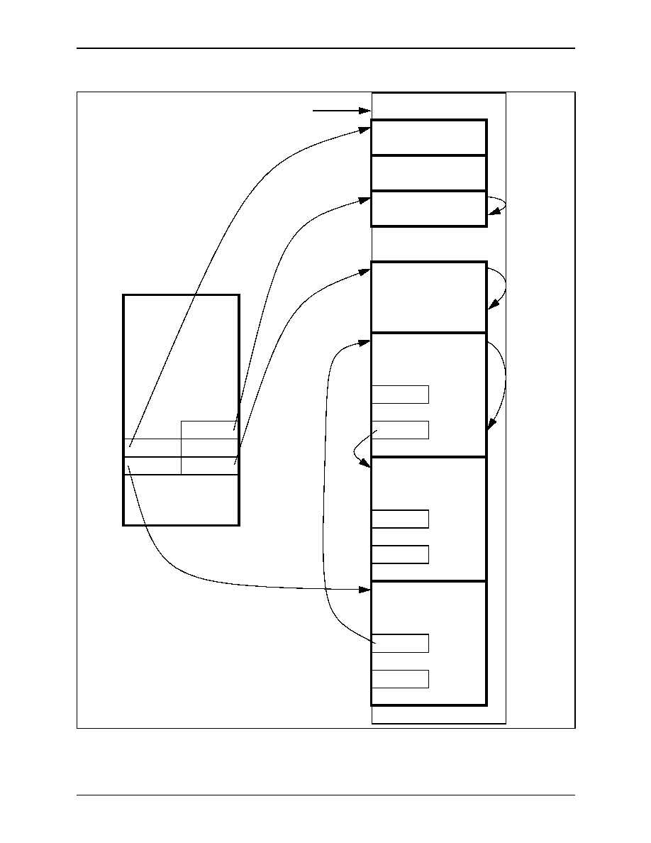
RS8234
6.0 Traffic Management
ATM ServiceSAR Plus with xBR Traffic Management
6.5 Traffic Management Control and Status Structures
28234-DSH-001-B
Mindspeed Technologies
TM
6-51
Figure 6-22. ABR Linkage
CELL_INDEX
FWD_INDEX
RATE_INDEX
EB_INDEX
ER SCH_STATE
SCH_ERB
ACDB
ACDB
ACDB
Exponent Table
ACDV
Exponent
ARDB
ACR_INDEX
NEW_RATEn
ARDB
ACR_INDEX
NEW_RATEn
ARDB
ACR_INDEX
NEW_RATEn
ARDV
6.0 Traffic Management
RS8234
6.5 Traffic Management Control and Status Structures
ATM ServiceSAR Plus with xBR Traffic Management
6-52
Mindspeed Technologies
TM
28234-DSH-001-B
6.5.7 RS_QUEUE
Table 6-31. RS_QUEUE Entry -- OAM-PM Reporting Information Ready for Transmission
Word 31 30 29 28 27 26 25 24 23 22 21 20 19 18 17 16 15 14 13 12 11 10 9
8
7
6
5
4
3
2
1
0
0
0000
OAM_PM
Rsvd
BLER
SEG_VCC_INDEX
1
BCK_TUC0
BCK_TUC01
2
TRCC0
TRCC0+1
3
Rsvd
Table 6-32. RS_QUEUE Entry -- Forward ER RM Cell Received
Word 31 30 29 28 27 26 25 24 23 22 21 20 19 18 17 16 15 14 13 12 11 10 9
8
7
6
5
4
3
2
1
0
0
0100
ER_FWD
Rsvd
SEG_VCC_INDEX
1
Rsvd
Table 6-33. RS_QUEUE Entry -- Backward ER RM Cell Received
Word 31 30 29 28 27 26 25 24 23 22 21 20 19 18 17 16 15 14 13 12 11 10 9
8
7
6
5
4
3
2
1
0
0
0101
ER_BCK
Rsvd
SEG_VCC_INDEX
1
Rsvd
BN
CI
NI
Rsvd
ER

RS8234
6.0 Traffic Management
ATM ServiceSAR Plus with xBR Traffic Management
6.5 Traffic Management Control and Status Structures
28234-DSH-001-B
Mindspeed Technologies
TM
6-53
6.5.8 Scheduler Internal SRAM Registers
NOTE:
FOR SAR INTERNAL USE ONLY!
Application program should ignore these registers.
The following graphic is a layout for the head and tail pointers.
Scheduler SRAM registers are located in the address range 0x1640-00x17FF.
Table 6-35
describes the memory map of these registers.
Table 6-34. RS_QUEUE Field Descriptions
Field Name
Description
OAM_PM
OAM PM backward reporting information ready for transmission.
BLER
Block Error Result.
SEG_VCC_INDEX
Segmentation VCC index for backward reporting OAM PM cell.
BCK_TUC0
TUC0 field in received forward monitoring cell. Written directly from Forward_RM cell.
BCK_TUC01
TUC01 field in received forward monitoring cell. Written directly from Forward_RM cell.
TRCC0
Total Received Cell Count with CLP=0.
TRCC0+1
Total Received Cell Count with CLP=0+1.
ER_FWD
Forward ER RM cell received.
SEG_VCC_INDEX
Segmentation VCC index for transmitted Backward ER RM cell.
ER_BCK
Backward ER RM cell received.
BN
Backward Explicit Congestion Notification bit from received RM cell.
CI
Congestion Indication bit from received RM cell.
NI
No Increase bit from received RM cell.
ER
Explicit Cell Rate field from received RM cell.
Figure 6-23. Head and Tail Pointers
8236_166
Head
31
16 15
0
Tail

6.0 Traffic Management
RS8234
6.5 Traffic Management Control and Status Structures
ATM ServiceSAR Plus with xBR Traffic Management
6-54
Mindspeed Technologies
TM
28234-DSH-001-B
Table 6-35. Scheduler Internal SRAM Memory Map
Address
Name
Description
0x1640-0x1643
PRI_PNTR0
Global priority 0.
0x1644-0x1647
PRI_PNTR1
Global priority 1.
0x1648-0x164B
PRI_PNTR2
Global priority 2.
0x164C-0x164F
PRI_PNTR3
Global priority 3.
0x1650-0x1653
PRI_PNTR4
Global priority 4.
0x1654-0x1657
PRI_PNTR5
Global priority 5.
0x1658-0x165B
PRI_PNTR6
Global priority 6.
0x165C-0x165F
PRI_PNTR7
Global priority 7.
0x1660-0x1663
PRI_PNTR8
Global priority 8.
0x1664-0x1667
PRI_PNTR9
Global priority 9.
0x1668-0x166B
PRI_PNTR10
Global priority p10.
0x166C-0x166F
PRI_PNTR11
Global priority 11.
0x1670-0x1673
PRI_PNTR12
Global priority 12.
0x1674-0x1677
PRI_PNTR13
Global priority 13.
0x1678-0x167B
PRI_PNTR14
Global priority 14.
0x167C-0x167F
PRI_PNTR15
Global priority 15.
0x1680-0x17FF
Reserved
Not implemented.

28234-DSH-001-B
Mindspeed Technologies
TM
7-1
7
7.0 OAM Functions
7.1 OAM Overview
OAM cells are ATM Layer management messages. These are generated by the
host on the segmentation side of the RS8234, and are detected and either
monitored or processed on the reassembly side of the RS8234.
ATM's OAM capabilities differentiate it from other less robustly managed
communication technologies. The RS8234 provides internal support for the
detection and generation of OAM traffic, including Performance Monitoring
(PM) OAM.
The RS8234 supports the F4 and F5 OAM flows according to ITU-T
Recommendation I.610. It also monitors the performance of up to 128 channels,
generating PM-OAM cells according to the same specification.

7.0 OAM Functions
RS8234
7.1 OAM Overview
ATM ServiceSAR Plus with xBR Traffic Management
7-2
Mindspeed Technologies
TM
28234-DSH-001-B
7.1.1 OAM Functions Supported
Refer to ITU-T Recommendation I.610 for complete information on the
structures and functions of OAM cell generation, detection, and processing.
Table 7-1 below lists the OAM functions of the F4 and F5 OAM flows, as
defined in Recommendation I.610.
The RS8234 internally supports the following functions as described in I.610:
�
Full Performance Monitoring functions (designed for estimating
transmission performance on any channel, and for reporting performance
estimations in the backward direction)
�
Detection of OAM cells, and routing them as directed by the host
�
Generation of OAM cells, as directed by the host
Implementation of the full range of functions in processing OAM cells will be
done at the software level due to the low bandwidth of OAM traffic (less than 1%
of the bandwidth of active connections).
Table 7-1. OAM Functions of the ATM Layer
OAM Function
Main Application
AIS (Alarm Indication Signal)
For reporting defect indications in the forward direction.
RDI (Remote Defect
Indication)
For reporting remote defect indications in the backward direction.
CC (Continuity Check)
For continuously monitoring the continuity of a connection. A continuity cell is used
periodically to check whether a connection is idle or has failed.
Loopback
Used for:
on-demand connectivity monitoring,
fault localization, and
pre-service connectivity verification.
PM (Performance
Monitoring)
For estimating performance and for reporting performance estimations in the backward
direction.
Activation/Deactivation
For activating/deactivating performance monitoring and continuity check.
System Management
(For use by end-systems only.)
RS8234
7.0 OAM Functions
ATM ServiceSAR Plus with xBR Traffic Management
7.1 OAM Overview
28234-DSH-001-B
Mindspeed Technologies
TM
7-3
7.1.2 OAM Flows Supported
7.1.2.1 F4 OAM Flow
The F4 OAM flow is the Virtual Path level, provided by OAM cells dedicated to
ATM layer OAM functions for Virtual Path Connections (VPCs). The F4 flow is
bidirectional.
There are two kinds of F4 OAM flows which can simultaneously exist in a
VPC:
�
end-to-end F4 flow (used for end-to-end VPC operations
communications); and
�
segment F4 flow (used for communicating operations information within
the bounds of one VPC link, such segment having its source and sink
defined by the user).
OAM cells for the F4 flow have the same VPI value as the user cells of the
VPC.
F4 flow OAM cells are identified as F4 flow cells by a pre-assigned VCI value
of three (segment flow cell) or four (end-to-end flow cell). The same pre-assigned
VCI value is used for both directions of the F4 flow.
7.1.2.2 F5 OAM Flow
The F5 OAM flow is the Virtual Channel level, provided by OAM cells dedicated
to ATM layer OAM functions for VCCs. The F5 flow is bidirectional.
There are two kinds of F5 OAM flows which can simultaneously exist in a
VCC:
�
end-to-end F5 flow (used for end-to-end VCC operations
communications); and
�
segment F5 flow (used for communicating operations information within
the bounds of one VCC link, such segment having its source and sink
defined by the user).
OAM cells for the F5 flow have the same VPI value and VCI value as the user
cells of the VCC.
F5 flow OAM cells are identified as F5 flow cells by a pre-assigned PTI code
value of 100 (segment flow cell) or 101 (end-to-end flow cell). The same
pre-assigned PTI value is used for both directions of the F5 flow.
Table 7-2. VCI Values for F4 OAM Flows
VCI Value
Interpretation
3
Segment OAM F4 flow cell
4
End-to-end OAM F4 flow cell
Table 7-3. PTI Values for F5 OAM Flows
PTI Code
Interpretation
100
Segment OAM F5 flow cell
101
End-to-end OAM F5 flow cell

7.0 OAM Functions
RS8234
7.1 OAM Overview
ATM ServiceSAR Plus with xBR Traffic Management
7-4
Mindspeed Technologies
TM
28234-DSH-001-B
7.1.2.3 Performance
Monitoring (PM)
Performance Monitoring includes a set of functions that monitor and process user
information on a channel to produce maintenance information specific to that
channel. This maintenance information is added to the in-rate data flow on that
channel in the form of PM cells; added at the source of a connection or link, and
extracted at the sink of a connection or link. With this maintenance information,
the user can estimate and analyze the transport integrity of that channel.
The PM flow is bidirectional, and PM cells are of two basic function types:
forward monitoring cells (which carry the forward error detection information),
and backward reporting cells (which carry the results of the performance
monitoring checks).
The RS8234 performs PM on up to 128 user-assigned channels. The SAR
enables PM for a channel by setting the PM enable bits (PM_EN) in the
Segmentation and Reassembly VCC State Table entries for that channel.
The RS8234 performs PM processing on any channel by monitoring blocks of
user cells on that channel. The size of this block of cells is set by the user, and can
have the value (N) of 128, 256, 512, or 1,024 cells. The RS8234 inserts a PM cell
after every N user cells on that channel. A block size of zero is valid when the
SAR is a destination point ONLY for PM processing. In this case, the
segmentation coprocessor will only generate Backward reporting cells in
response to reassembly performance monitoring calculations.
PM as performed by the RS8234 calculates the following:
�
Errored blocks (by means of a BIP-16 error detection code generated over
the payloads of the user cells in the PM block)
�
A count of misinserted PM forward monitoring cells
The user can activate PM on any channel either during connection
establishment, or at any time after the connection has been established.
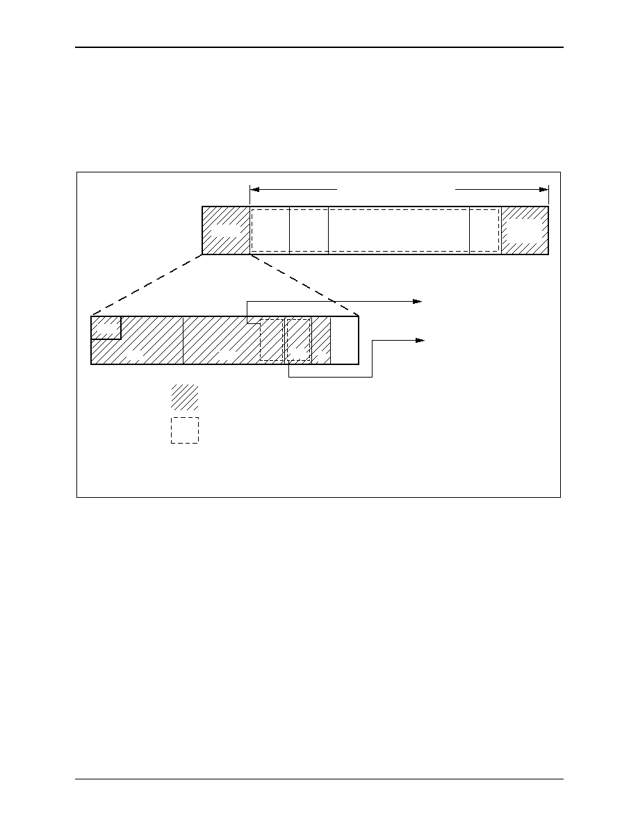
RS8234
7.0 OAM Functions
ATM ServiceSAR Plus with xBR Traffic Management
7.1 OAM Overview
28234-DSH-001-B
Mindspeed Technologies
TM
7-5
7.1.3 OAM Cell Format
Figure 7-1
illustrates the common OAM cell format and identifies the fields
specific to OAM.
Figure 7-1. OAM Cell Format
OAM Cell Information Fields
Cell Header
OAM
Type
Function
Type
Function Specific Fields
(Rsvd)
EDC
(CRC-10)
Header
HEC
VPI
VCI
PTI
L
GFC
5 octets
2 octets
45 octets
4 bits
3 bits
8 bits
8 bits
1 bit
4 bits
4 bits
6 bits
10 bits
4 bits
8 bits
12 bits
F4 Flow (VP)
VCI 3 = Segment
VCI 4 = End-to-end
F5 Flow (VC)
PTI 100 = Segment
PTI 101 = End-to-end
= Generated by the RS8234 for all OAM Cells.
= Generated by the RS8234 for PM OAM only.
NOTE(S): EDC = Error Detection Code (10 bits). This is a CRC-10 error detection code computed over the
OAM cell information fields, excluding the EDC field.
100074_061
7.0 OAM Functions
RS8234
7.1 OAM Overview
ATM ServiceSAR Plus with xBR Traffic Management
7-6
Mindspeed Technologies
TM
28234-DSH-001-B
The OAM Type and Function Type identifiers as specified by I.610, are listed
in Table 7-4.
.
Table 7-4. OAM Type and Function Type Identifiers
OAM Type
(1)
Coding
Function Type
(2)
Coding
Fault Management
0001
AIS
RDI
Continuity Check
Loopback
0000
0001
0100
1000
Performance Management
0010
Forward monitoring
Backward reporting
0000
0001
Activation/Deactivation
1000
Performance Monitoring
Continuity Check
0000
0001
System Management
1111
NOTE(S):
(1)
OAM Type indicates the type of management function performed by this cell; e.g., Fault Management, Performance
Management, etc.
(2)
Function Type indicates the actual function performed by this cell within the management type indicated by the
OAM Type field.

RS8234
7.0 OAM Functions
ATM ServiceSAR Plus with xBR Traffic Management
7.2 Segmentation of OAM Cells
28234-DSH-001-B
Mindspeed Technologies
TM
7-7
7.1.4 Local vs. Host Processing of OAM
ATM carries with it significant network management overhead. The RS8234
supports those robust OAM features described previously. Due to the breadth of
ATM applications and the continuing evolution of ATM management standards, it
is essential that a range of flexibility be provided in the processing of network
management overhead. To provide this flexibility, the RS8234 includes an
optional local processor interface.
Since the RS8234 is capable of SAR shared memory segmentation and
reassembly, it can route OAM traffic including PM traffic to and from this local
processor, thereby off-loading ATM network management from the host. Thus,
host processing power is focused on the user applications specifically concerned
with processing ATM user data traffic.
To accomplish this, the RS8234 provides global OAM buffer and status
queues (OAM_BFR_QU and OAM_STAT_QU, addresses for both assigned in the
RSM_CTRL1 register). If the OAM_QU_EN bit in the RSM_CTRL1 register is
set to a logic high, then the RS8234 routes OAM traffic to these global queues.
And with SAR shared memory addresses assigned to these global queues, the
RS8234 processes OAM traffic through the local processor, thereby freeing the
host from these management functions. As well, the global OAM segmentation
status queue, SEG_CTRL(OAM_STAT_ID), is used if the OAM_STAT bit in the
segmentation buffer descriptor is a logic high.
7.2 Segmentation of OAM Cells
The host (or local processor) places OAM cells in a single buffer, and thus
allocates a single segmentation buffer descriptor (SBD) for the OAM cell data
buffer, not a linked list of SBDs.
The host (or local processor) then writes a pointer to that SBD in the next
available transmit queue entry, and sets the VLD bit to one.
When the segmentation coprocessor processes that transmit queue entry, it
submits the OAM cell data buffer to the xBR Traffic Manager and the cell thus is
scheduled for transmission.

7.0 OAM Functions
RS8234
7.2 Segmentation of OAM Cells
ATM ServiceSAR Plus with xBR Traffic Management
7-8
Mindspeed Technologies
TM
28234-DSH-001-B
7.2.1 Key OAM-Related Fields for OAM Segmentation
7.2.1.1 Segmentation
Buffer Descriptors
Several fields in the SBD entry are used to facilitate segmentation of OAM cells.
�
Set the 2-bit AAL_OPT field to SINGLE (value = 01). This enables
reading 48 octets from a single buffer to form a single ATM cell.
�
Set the OAM_STAT bit to a logic high. The RS8234 will now report status
to the OAM-dedicated OAM_STAT_ID identified in the SEG_CTRL
register, instead of the STAT specified in the SEG VCC Table entry.
�
Set the single-bit HEADER_MOD field to a logic one. This activates the
WR_PTI and WR_VCI bits in the buffer descriptor, which signal the
RS8234 to overwrite the ATM header PTI and VCI fields for that cell with
the values from the PTI_DATA and VCI_DATA fields. In this way, F4 and
F5 flow OAM cells can be generated by the RS8234.
�
The VCI_DATA field set to a value of three (segment cell) or four
(end-to-end cell) generates an F4 flow OAM cell.
�
The PTI_DATA field set to a value of 100 (segment cell) or 101
(end-to-end cell) generates an F5 flow OAM cell.
�
Set the AAL_MODE field to 01 (AAL0).
�
Set both BOM and EOM bits to zero.
�
Set the CRC10 bit to a logic high.
7.2.1.2 Low Latency
Transmission
For low latency, the LINK_HEAD bit in the transmit queue entry should be set to
a logic high. This tells the RS8234 to link the buffer chain at the head of the
existing chain for the corresponding VCC. This bit is intended for use with the
SEG buffer descriptor's SINGLE option, to send in-line OAM cells. Only a single
SEG buffer descriptor may be linked to a transmit queue entry when this bit is set.
This bit must also be set if the OAM SBD is placed on the transmit queue after
a partial PDU, to ensure correct segmentation.
7.2.1.3 Segmentation
Status Queue
The SINGLE bit in the SEG status queue entry should be set to a logic high. This
bit is set if the SINGLE option in the AAL_OPT field of the SEG buffer
descriptor is set. This bit indicates a special buffer is in use, rather than the
normal system-assigned buffers for normal CPCS-PDUs.
7.2.1.4 F4 Flow
For F4 flow operation, a separate VCC Table entry must be configured.
7.2.2 Error Condition During OAM Segmentation
Each OAM cell has a 10-bit Error Detection Code (EDC) field, for storing and
transporting the calculated CRC-10 error detection code results (computed over
the OAM cell information fields, excluding the EDC field). To enable this
CRC-10 function, set the CRC10 bit in the SEG buffer descriptor entry to a logic
high.

RS8234
7.0 OAM Functions
ATM ServiceSAR Plus with xBR Traffic Management
7.3 Reassembly of OAM Cells
28234-DSH-001-B
Mindspeed Technologies
TM
7-9
7.3 Reassembly of OAM Cells
To enable the reassembly coprocessor to detect and therefore further process
OAM cells, set the OAM_EN bit in RSM_CTRL1 to a logic high.
The RS8234 detects the following OAM cell flows:
�
Segment F4 Flow
�
End-to-end F4 Flow
�
Segment F5 Flow
�
End-to-end F5 Flow
�
PTI = 6
�
PTI = 7
The RS8234 provides global OAM buffer and status queues (OAM_BFR_QU
and OAM_STAT_QU, addresses for both assigned in the RSM_CTRL1 register).
To activate these queues, set the OAM_QU_EN bit in the RSM_CTRL1 register
to a logic high. The RS8234 then routes OAM traffic to these global buffer and
status queues.
NOTE:
The cell buffer size must be large enough to hold a complete cell, when
OAM detection is enabled.
7.3.1 Key OAM-Related Fields for OAM Reassembly
7.3.1.1 Reassembly
VCC State Table
The reassembly VCC State Table field, SEG_VCC_INDEX, should be written to
point to the channel index of the corresponding segmentation channel. This is
necessary for PM-OAM, as well as ABR channels.
7.3.1.2 Reassembly
Status Queue
The 3-bit OAM field in the RSM status queue entry should be set to the value
indicated in the RSM status queue structure description for that field. A non-zero
value in the OAM field indicates that the cell is an OAM cell.
If the CRC-10 error detection code computation on the OAM cell shows an
error, the RS8234 will set the CRC_ERROR bit in the status queue entry to a
logic high.
7.3.1.3 F4 Flow
For F4 flow operation, a separate VCC Table entry must be configured.

7.0 OAM Functions
RS8234
7.3 Reassembly of OAM Cells
ATM ServiceSAR Plus with xBR Traffic Management
7-10
Mindspeed Technologies
TM
28234-DSH-001-B
7.3.2 OAM Reassembly Operation
Received OAM traffic should be detected and routed to the global OAM buffer
and status queues (OAM_BFR_QU and OAM_STAT_QU).
The reassembly coprocessor treats OAM cells as one-cell PDUs. The RSM
coprocessor transfers the 48-octet OAM payload to the next available global data
buffer, and writes a RSM status queue entry.
Once an OAM cell is detected, the RSM coprocessor checks the cell to
determine whether it is a PM cell, by seeing if the OAM_TYPE field in the cell is
set to value "0010". Note that PM detection is only performed on F4 and F5 OAM
cells.
If the RSM coprocessor finds the cell is a PM cell, it is processed following
the guidelines described in
Section 7.4
.
NOTE:
OAM cells that get buffers from the global OAM free buffer queue do not
effect the per-VCC firewall calculation.
7.3.3 Error Conditions During OAM Reassembly
The RSM coprocessor computes the CRC-10 error detection code each received
OAM cell's information fields. If an error is detected (i.e., the computed CRC
value does not match the CRC-10 value written in the cell), the SAR sets the
CRC_ERROR bit in the status queue entry to a logic high.
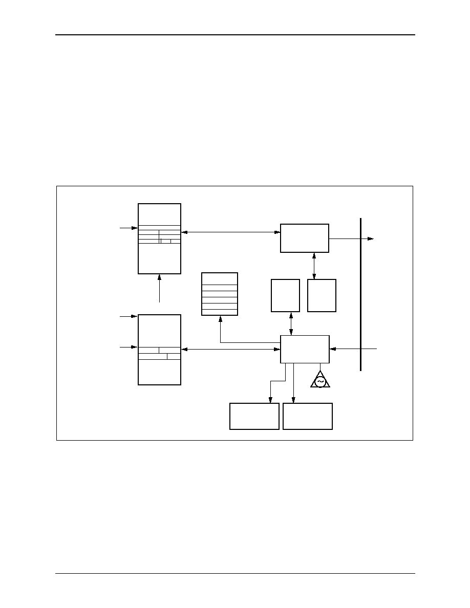
RS8234
7.0 OAM Functions
ATM ServiceSAR Plus with xBR Traffic Management
7.4 PM Processing
28234-DSH-001-B
Mindspeed Technologies
TM
7-11
7.4 PM Processing
OAM Performance Monitoring may be enabled for up to 128 VCCs by setting the
PM_EN bits in the RSM VCC Table entry and the SEG VCC Table entry for that
channel.
Figure 7-2 illustrates the functional blocks for PM processing.
Figure 7-2. Functional Blocks for PM Segmentation and Reassembly
SEG_PM Table
RSM_PM Table
OAM_BFR_QU
OAM_STAT_QU
PM_INDEX
PM_INDEX
Top of VPI Index
Table, +64 bytes
RS_Queue
Segmentation
Coprocessor
RSM
VCC
Table
SEG
VCC
Table
Reassembly
Coprocessor
(Global OAM Rsm
Buffer Queue)
(Global OAM Rsm
Status Queue)
(BIP-16 Calculation)
PHY
100074_062
7.0 OAM Functions
RS8234
7.4 PM Processing
ATM ServiceSAR Plus with xBR Traffic Management
7-12
Mindspeed Technologies
TM
28234-DSH-001-B
For any channel on which PM processing is enabled, the RS8234 performs
these functions:
�
The RSM coprocessor reassembles received PM-OAM cells in the global
reassembly OAM buffer queue (OAM_BFR_QU).
�
A reassembly status record is written to the global reassembly OAM status
queue, for each received PM-OAM cell. The status entry for a forward
monitoring PM-OAM cell includes the Block Error Result (BIPV)
calculation, and both Total Received Cell Counts (TRCC0 and TRCC0+1).
The two Total User Cell number fields (TUC0 and TUC0+1) can be
extracted directly from the cell payload.
�
The RSM coprocessor performs the BIP-16 calculation on each received
data cell in the defined PM block, and writes this data to the RSM_PM
table entry set aside for that PM_INDEX.
�
For each forward monitoring PM cell received, the RSM coprocessor
writes an entry for a backward reporting PM cell in the RS_Queue,
causing the RS8234 to generate and transmit a backward reporting PM
cell.
�
The segmentation coprocessor automatically generates a forward
monitoring PM cell at the end of each PM block. It gets the data for these
cells from the SEG_PM table entry for that PM_INDEX. This can be
optionally disabled by setting the FWD_MON field equal to zero.
7.4.1 Initializing PM Operation
The user must initialize the fields described in
Table 7-5
before starting PM
processing:
Table 7-5. PM-OAM Field Initialization For Any PM_INDEX
Register / Table
Field
Initialized Value
Notes
RSM_CTRL1
(Reassembly Control
Register 1)
OAM_EN
0-1
OAM_QU_EN
0-1
OAM_BFR_QU
(User assigned)
OAM_STAT_QU
(User assigned)
SEG_PMBASE
(SEG PM Base Register)
SEG_PMB[15:0]
(User assigned)
Base address for SEG_PM table.

RS8234
7.0 OAM Functions
ATM ServiceSAR Plus with xBR Traffic Management
7.4 PM Processing
28234-DSH-001-B
Mindspeed Technologies
TM
7-13
7.4.2 Setting Up Channels for PM Operation
When the RS8234 receives a PM activation cell (OAM Type = 1000, Function
Type = 0000), or when the user decides to activate PM processing on a channel,
the host (or local) processor must enable PM on the applicable channel by setting
the PM_EN bits in the RSM and SEG VCC Table entries to logic high, and
selecting an unused PM_INDEX (0-127).
The host would then initialize the corresponding SEG_PM and RSM_PM
table entries. The format of each entry of the SEG_PM table is illustrated in
Table 7-6
and the format of each entry of the RSM_PM Table is illustrated in
Table 7-8
.
The assigned PM_INDEX value for that channel will have to be written to
both the RSM VCC Table entry and the SEG VCC Table entry for that channel.
For F4 flows, each VCI channel in the VPI group must have the PM_EN bits
in both the RSM VCC Table entry and the SEG VCC Table entry set high, and the
PM_INDEX pointing to the same location. In addition, a RSM and SEG VCC
Table entry must be configured corresponding to VCI=3 or VCI=4.
To initialize backward reporting without forward monitoring on any channel,
set FWD_MON = 0.
Once the SEG_PM and RSM_PM table entries have been initialized, the
processor will send an activation confirmed OAM cell to the originator.
7.4.3 PM Operation
PM processing operates automatically on any channel until stopped by clearing
the PM_EN fields in the SEG VCC Table entry and the RSM VCC Table entry.
PM-OAM cells are not included in the NRM cell count, as part of ER
processing. See
Chapter 6.0
for details.
7.4.3.1 Generation of
Forward Monitoring PM
Cells
The segmentation coprocessor generates a forward monitoring PM cell at the end
of each PM block, as defined by the BLOCK_SIZE field in the SEG_PM table
for any PM_INDEX. It determines the point to generate a forward monitoring cell
by following these processes:
�
At the point of initialization of PM processing or when a forward
monitoring cell is sent, the SEG coprocessor sets the BLOCK_COUNT
field to zero. It also increments Monitoring Cell Sequence Number
(MSN), and re-initializes the BIP field to zero.
�
As each data cell is segmented, the SEG coprocessor increments the
BLOCK_COUNT number and updates the BIP field.
�
When the BLOCK_COUNT number reaches the block size specified by
the BLOCK_SIZE field, signifying the end of the PM block, the SEG
coprocessor generates a new forward monitoring PM cell and starts these
processes again.

7.0 OAM Functions
RS8234
7.4 PM Processing
ATM ServiceSAR Plus with xBR Traffic Management
7-14
Mindspeed Technologies
TM
28234-DSH-001-B
7.4.3.2 Reassembly of
Forward Monitoring PM
Cells
When the RS8234 receives a forward monitoring PM cell, the RSM coprocessor
reads the RSM_PM table word pointed to by the PM_INDEX field in the RSM
VCC Table entry. The location of the RSM_PM Table is above the LECID Table.
The BIPV, TRCC0, and TRCC0+1 fields are written to a special RSM-PM
forward monitoring status queue entry. The TUC0 and TUC0+1 fields can be
extracted directly from the RSM_PM cell payload.
When a new buffer is needed, the reassembly coprocessor uses the global
OAM buffer queue if RSM_CTRL1(OAM_QU_EN) is a logic high. Otherwise, it
uses the BFR0 pool identification number in the RSM VCC Table to point to the
appropriate free buffer queue.
A RSM status entry is written for each OAM cell reassembled.
The reassembly coprocessor uses the global OAM status queue if the
RSM_CTRL1(OAM_QU_EN) bit is a logic high. Otherwise, it uses the STAT
field in the RSM VCC Table to determine which status queue to use for that
channel.
7.4.3.3 Reassembly of
Backward Reporting PM
Cells
Backward reporting cells are reassembled in the same manner as non-PM OAM
cells.
7.4.3.4 Turnaround and
Segmentation of
Backward Reporting PM
Cells
For each forward monitoring cell received, the RS8234 also writes the BIPV,
TRCC0, TRCC0+1, TUC0, and TUC0+1 fields to the RS_Queue, for further
processing by the segmentation coprocessor. The segmentation coprocessor
generates a backward reporting cell.
7.4.3.5 Turnaround of
Backward Reporting PM
Cells ONLY
To enable turnaround of backward reporting PM cells without generation of
forward monitoring PM cells, set the segmentation PM_EN bit in the SEG VCC
Table entry to a logic high, set the PM_INDEX, and set the FWD_MON field to
zero.
7.4.4 Error Conditions During PM Processing
If OAM cells are not using the global reassembly OAM buffer pool, then the cells
are treated as Single Segment Messages (SSMs) for purposes of the firewall
protection. OAM cells using the global OAM buffer pool do not have per channel
protection.
If the RS_Queue fills, the PM-OAM information will be dropped, and the
RS_QUEUE_FULL status indication will be set.
7.4.5 PASS_OAM Function
A PASS_OAM only function is activated by setting bit 22 of word 0 in the RSM
VCC table. When active, OAM cells are processed, and data cells are discarded
without incrementing any discard counters.

RS8234
7.0 OAM Functions
ATM ServiceSAR Plus with xBR Traffic Management
7.5 OAM Control and Status Structures
28234-DSH-001-B
Mindspeed Technologies
TM
7-15
7.5 OAM Control and Status Structures
Refer to the "Control and Data Structures" sections of
Chapter 4.0
and
Chapter 5.0
for information on VCC Tables, buffer descriptors, the transmit
queue, and status queues, as they apply to generating and processing OAM cells.
The base address of the SEG_PM table is given by the SEG_PMB field in the
SEG_PMBASE register. The address of each entry is located at byte address,
SEG_PMB*128 + <PM_INDEX>*32.
The RSM_PM table is located above the LECID table, which is located above the
VPI table. The address of each entry is located at byte address,
if RSM_CTRL0(VPI_MASK)
RSM_ITB*128 + 1024 + 64 + <PM_INDEX>*16
else
RSM_ITB*128 + 16384 + 64 + <PM_INDEX>*16
7.0 OAM Functions
RS8234
7.5 OAM Control and Status Structures
ATM ServiceSAR Plus with xBR Traffic Management
7-16
Mindspeed Technologies
TM
28234-DSH-001-B
7.5.1 SEG_PM Structure
Table 7-6 and Table 7-7 describe the structure and field definitions of the
SEG_PM table.
Table 7-6. SEG_PM Structure
Word 31 30 29 28 27 26 25 24 23 22 21 20 19 18 17 16 15 14 13 12 11 10 9
8
7
6
5
4
3
2
1
0
0
ATM_HEADER
1
FWD_TUC0
FWD_TUC01
2
FW
D
_
P
M
BL
OC
K_
SIZ
E
FW
D
_
MO
N
Rsvd
BLOCK_COUNT
BIP
3
Rsvd
BLER
BCK_MSN
FWD_MSN
4
BCK_TUC0
BCK_TUC01
5
TRCC0
TRCC01
6
Reserved
7
Reserved
Table 7-7. SEG_PM Field Descriptions
Field Name
Description
ATM_HEADER
ATM header to use for both backward reporting and forward monitoring cells.
FWD_TUC0
Total User Cell number with CLP=0 for forward monitoring.
FWD_TUC01
Total User Cell number with CLP=0,1 for forward monitoring.
FWD_PM
Initialized to zero. Set to one when BLOCK_COUNT reaches its BLOCK_SIZE limit, signifying that a
PM cell is ready to forward.
BLOCK_SIZE
Size in cells of forward monitoring block:
00: block size = 128
01: block size = 256
10: block size = 512
11: block size = 1,024
FWD_MON
Set to enable both forward monitoring and backward reporting.
Clear to enable only backward reporting.
BLOCK_COUNT
Number of cells in current monitoring block.
BIP
BIP-16 for forward monitoring.
BLER
Block Error Result for backward reporting cells.
BCK_MSN
Monitoring Cell Sequence Number for backward reporting cells.
FWD_MSN
Monitoring Cell Sequence Number for forward monitoring cells.
BCK_TUC0
TUC0 field for backward reporting cells.
BCK_TUC01
TUC01 field for backward reporting cells.
TRCC0
Total Received Cell Count with CLP=0 for backward reporting.
TRCC01
Total Received Cell Count with CLP=0,1 for backward reporting.
RS8234
7.0 OAM Functions
ATM ServiceSAR Plus with xBR Traffic Management
7.5 OAM Control and Status Structures
28234-DSH-001-B
Mindspeed Technologies
TM
7-17
7.5.2 RSM_PM Table
Table 7-8
and
Table 7-9
describe the structure and definitions of the RSM_PM
table.
Table 7-8. RSM_PM Table Entry
Word 31 30 29 28 27 26 25 24 23 22 21 20 19 18 17 16 15 14 13 12 11 10 9
8
7
6
5
4
3
2
1
0
0
Rsvd
MSN
1
BIP16
BCNT
2
TRCC0
TRCC0+1
3
Rsvd
Table 7-9. RSM_PM Table Field Descriptions
Field Name
Description
BIP16
The BIP-16 error detection code generated over the payloads of the user information cells in the PM
block.
BCNT
Block Count. This field contains the calculated number of cells in the current PM block.
MSN
Monitoring Cell Sequence Number for forward monitoring PM cells. Backward reporting PM cells are
not included in this sequence. This field allows for the detection of lost or mis-inserted PM cells
containing forward monitoring information.
TRCC0
Total received cell count with CLP = 0.
TRCC0+1
Total received cell count.

7.0 OAM Functions
RS8234
7.5 OAM Control and Status Structures
ATM ServiceSAR Plus with xBR Traffic Management
7-18
Mindspeed Technologies
TM
28234-DSH-001-B

28234-DSH-001-B
Mindspeed Technologies
TM
8-1
8
8.0 DMA Coprocessor
8.1 Overview
The DMA coprocessor is intended to perform high-speed sustained data transfers
to and from the host memory space. It is controlled by the segmentation and
reassembly coprocessors.
The major functions of the DMA coprocessor are to transfer data from the
host memory (through the PCI bus) to the segmentation coprocessor, and to
transfer data from the reassembly coprocessor to the host memory space (through
the PCI bus).
In all modes of operation, the DMA coprocessor maintains a high level of
performance. It uses burst transfers when possible to maximize utilization of the
host bus bandwidth, performs byte switching to accommodate misaligned
transfers, and carries out concurrent input and output transfers (alternating burst
reads and burst writes) to support simultaneous input and output data streams.
8.2 DMA Read
For outgoing messages, DMA read cycles move data from host memory to the
segmentation coprocessor using a gather DMA method. The maximum burst size
is thirteen 32-bit words, which correspond to one cell. The burst size can be
reduced by setting the MAX_BURST_LEN field in the PCI Configuration
Register at a value less than 13 words.
8.3 DMA Write
For incoming messages, DMA write cycles move data from the reassembly
coprocessor to host memory using a scatter DMA method. The maximum burst
size is fourteen 32-bit words, which correspond to one ATM cell and a status
word appended to PM cells. The burst size can be reduced by setting the
MAX_BURST_LEN field in the PCI Configuration Register at a value less than
13 words.
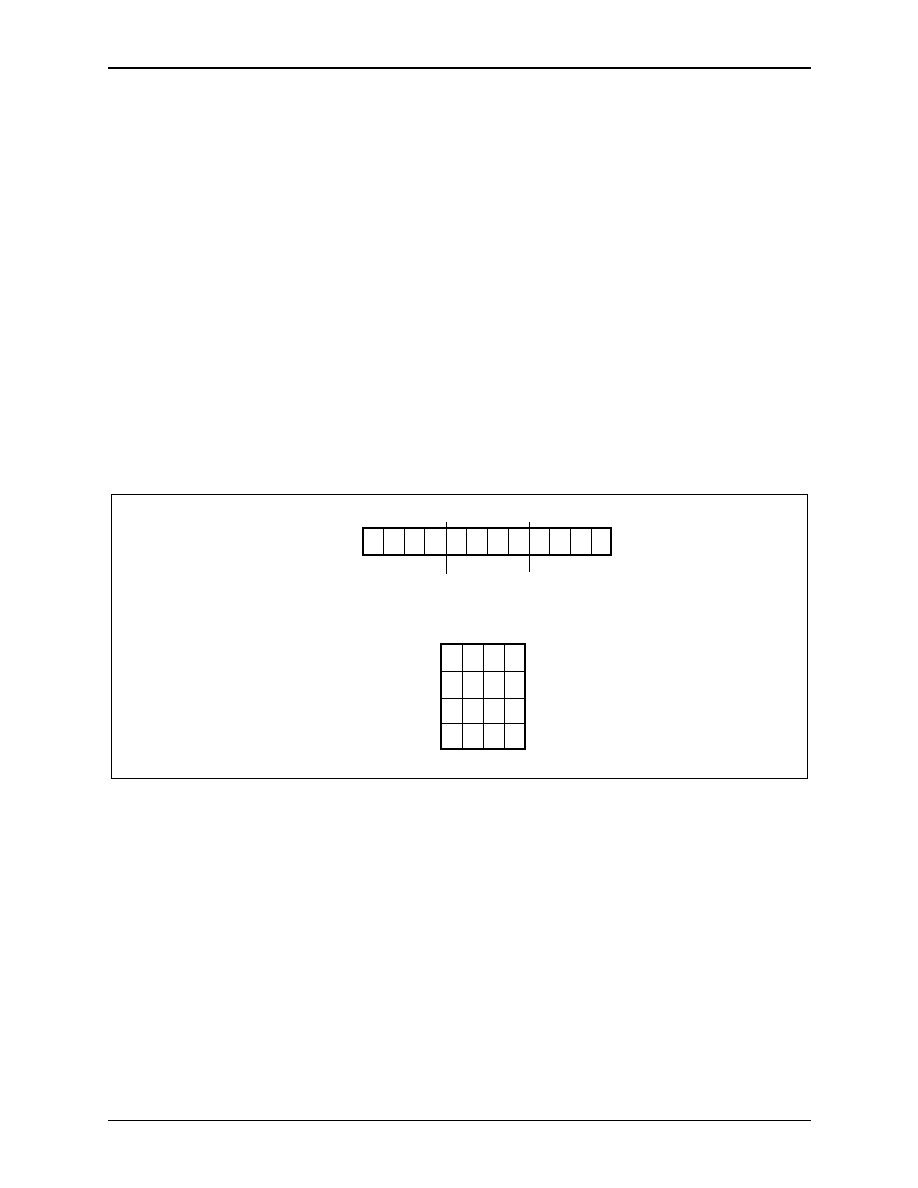
8.0 DMA Coprocessor
RS8234
8.4 Misaligned Transfers
ATM ServiceSAR Plus with xBR Traffic Management
8-2
Mindspeed Technologies
TM
28234-DSH-001-B
8.4 Misaligned Transfers
The reassembly and segmentation coprocessors handle data internally on word
addresses. The DMA coprocessor must be capable of handling transfers from the
PCI bus without the same constraint, i.e., with data that is not aligned on word
boundaries. In addition, the length of the transfer is specified in bytes, not 32-bit
words, even though the data bus widths are all 32 bits.
To facilitate this, byte-switching logic is used within the RS8234. When the
RS8234 specifies a host address with the Least Significant Bits (LSBs) = 00, it is
implied that the data is byte aligned.
Figure 8-1
shows how a byte-aligned address
would map into the PCI host address space for a little endian system. Selecting
between big and little endian systems is done using the ENDIAN [bit 12] in
Configuration Register 0 [CONFIG0;0x14].
Figure 8-1. LIttle Endian Aligned Transfer
ATM Cell
0
0
1
1
2
2
3
3
4
5
6
7
4
5
6
7
8
8
9
9
Host Address = 00 from RSM block
0x00
0x04
0x08
Address
10
10
11
11
Length(# of 32 bit words) = 3
Bytes
PCI Host Address Space
100074_063
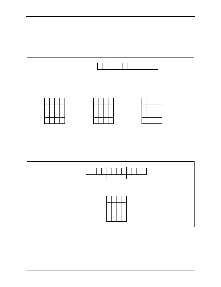
RS8234
8.0 DMA Coprocessor
ATM ServiceSAR Plus with xBR Traffic Management
8.4 Misaligned Transfers
28234-DSH-001-B
Mindspeed Technologies
TM
8-3
When the RS8234 specifies a host address with the LSBs not equal to 00, it is
implied that the data is misaligned.
Figure 8-2
shows how a misaligned address
would map into the PCI host address space for a little endian system.
Figure 8-3
shows how a byte-aligned address would map into the PCI host
address space for a big endian system.
Figure 8-2. Little Endian Misaligned Transfer
ATM Cell
0
0
0
0
1
1
1
1
2
2
2
2
3
3
3
3
4
4
4
4
5
5
5
5
6
6
6
6
7
7
7
7
8
8
8
8
9
9
9
9
Host Address = 11
0x00
0x04
0x08
0x0C
Address
Host Address = 10
0x00
0x04
0x08
0x0C
0x0C
Address
Host Address = 01
0x00
0x04
0x08
Address
10
10
10
10
11
11
11
11
Length (# of 32 bit words) = 3
PCI Host Address Space
Bytes
Bytes
Bytes
from RSM block
from RSM block
from RSM block
100074_064
Figure 8-3. Big Endian Aligned Transfer
0
0
1
1
2
2
3
3
4
4
5
5
6
6
7
7
8
8
9
9
0x00
0x04
0x08
Address
10
10
11
11
Bytes
ATM Cell
PCI Host Address Space
Length (# of 32 bit words) = 3
Host Address = 00 from RSM block
100074_065
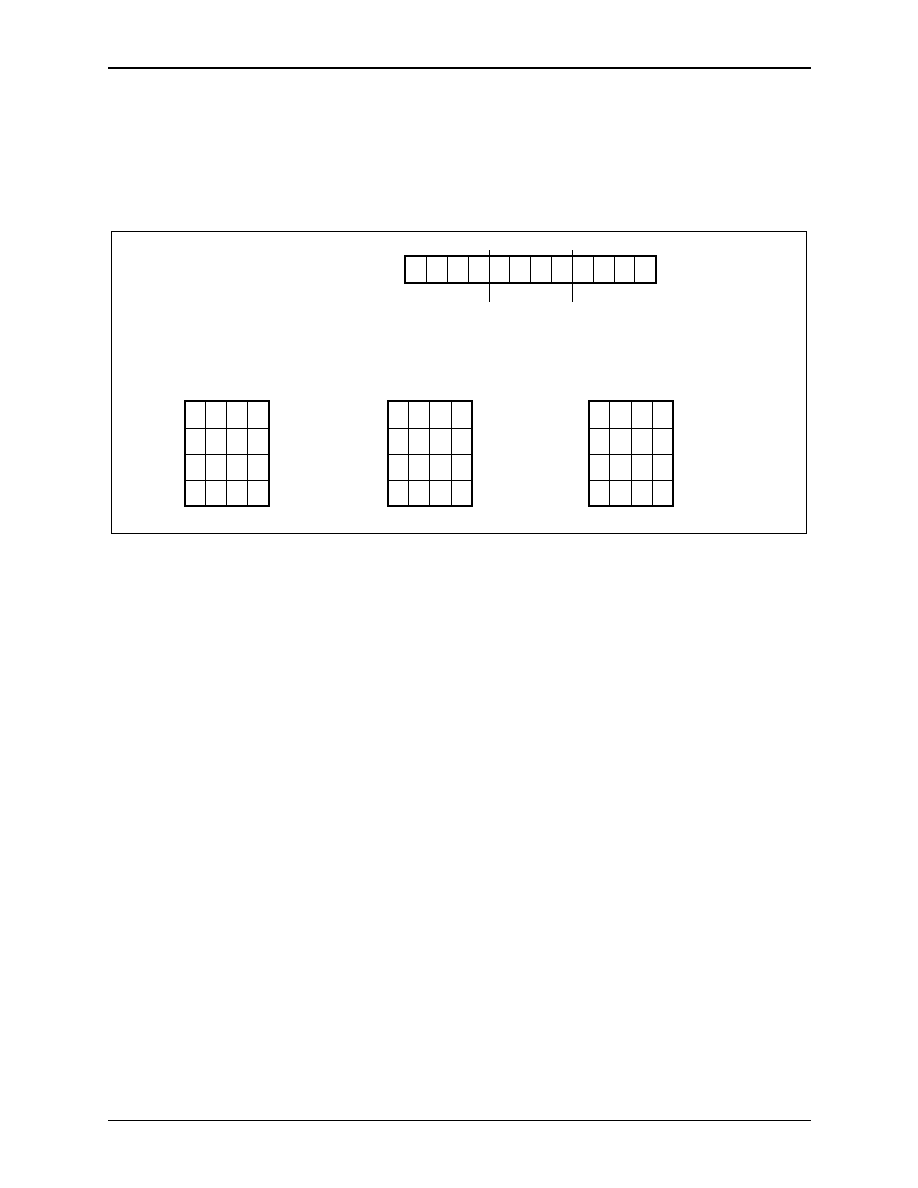
8.0 DMA Coprocessor
RS8234
8.5 Control Word Transfers
ATM ServiceSAR Plus with xBR Traffic Management
8-4
Mindspeed Technologies
TM
28234-DSH-001-B
When the RS8234 specifies a host address with the LSBs not equal to 00, it is
implied that the data is not aligned.
Figure 8-4
shows how an unaligned address
would map into the PCI host address space for a big endian system.
8.5 Control Word Transfers
If a host system sends control words to the SAR in little endian format, the
reassembly and segmentation blocks must have the capability of byte swapping, to
format these control words to or from big endian.
Control word byte swapping is controlled by bits 30 (Master Control Byte
Swap, MSTR_CTRL_SWAP) and 29 (Slave Control Byte Swap, SLAVE_
SWAP), located in the Special Status Register of the PCI Configuration Space
(address 0x40).
When SLAVE_SWAP is a logic high, the slave interface swaps the bytes of a
slave write or read access. When MSTR_CTRL_SWAP is a logic high, the
control structures that the SAR writes are written with bytes swapped.
An active HRST* will cause these bits to be a logic low.
Figure 8-4. Big Endian Misaligned Transfer
ATM Cell
0
0
0
0
1
1
1
1
2
2
2
2
3
3
3
3
4
4
4
4
5
5
5
5
6
6
6
6
7
7
7
7
8
8
8
8
9
9
9
9
Host Address = 11
0x00
0x04
0x08
0x0C
Address
Host Address = 10
0x00
0x04
0x08
0x0C
0x0C
Address
Host Address = 01
0x00
0x04
0x08
Address
10
10
10
10
11
11
11
11
Length (# of 32 bit words) = 3
PCI Host Address Space
Bytes
Bytes
Bytes
from RSM block
from RSM block
from RSM block
100074_066

28234-DSH-001-B
Mindspeed Technologies
TM
9-1
9
9.0 Local Memory Interface
9.1 Overview
To simplify system implementations, the RS8234 integrates a complete memory
controller, designed for direct interface to common SRAMs. The control and
status registers, as well as the physical interface devices in the standalone mode of
operation, are mapped into the bottom of the memory map. Consequently,
accesses to these resources are also controlled by the memory controller.
Up to 8 MB of external memory using SRAM devices can be accessed by the
RS8234. The amount of memory required is heavily dependent on the number of
VCCs implemented, as well as the number of VCCs that are currently active.
Memory requirements are discussed further in
Section 9.3
.

9.0 Local Memory Interface
RS8234
9.1 Overview
ATM ServiceSAR Plus with xBR Traffic Management
9-2
Mindspeed Technologies
TM
28234-DSH-001-B
Figure 9-1
shows the RS8234 address map.
Figure 9-1. RS8234 Memory Map
MCS[3]*
MCS[2]*
MCS[1]*
MCS[0]*
PHYCS2*
PHYCS1* (CN8250)
(1)
(1)
RS8234 Internal Registers
(0x7FFFFFh >> (5-BANKSIZE))
(0x600000h >> (5-BANKSIZE))
(0x5FFFFFh >> (5-BANKSIZE))
(0x400000h >> (5-BANKSIZE))
(0x3FFFFF >> (5-BANKSIZE))
(0x200000h >> (5-BANKSIZE))
(0x1FFFFFh >> (5-BANKSIZE))
0x001800h
0x000800h�0x000FFFh
0x000200h�0x0007FFh
0x000000h�0x0001FFh
0x001000h-0x0017FFh
Internal SRAM
100074_067
NOTE(S): All addresses in this illustration are byte addresses.
(1)
These device selects are available in stand-alone mode only; otherwise, this memory is mapped to MSC[0]*.

RS8234
9.0 Local Memory Interface
ATM ServiceSAR Plus with xBR Traffic Management
9.2 Memory Bank Characteristics
28234-DSH-001-B
Mindspeed Technologies
TM
9-3
9.2 Memory Bank Characteristics
The external memory is organized in one to four banks of up to 2 MB each. The
system may use any number of banks to fulfill the memory requirements, the only
stipulation is that the banks must be of the same size and organization. The local
processor and Host processor select between the banks via the PBSEL[1:0]
inputs. PBSEL[1:0] is sourced by local processor Host processor sources PCI
Address Bits. BANKSIZE[2:0] (bits 23�21) in the CONFIG0 register denote the
size of the memory banks and allow the RS8234 to incorporate the various bank
sizes into contiguous memory.
Table 9-1
gives the coding of the BANKSIZE[2:0]
control bits.
The memory controller is designed to work with standard by_8 and by_4
SRAM devices, as well as with by_16 devices. Grounding the RAMMODE input
selects the by_4 or by_8 mode of operation, while pulling RAMMODE to a logic
one selects by_16 operation. When by_16 operation is selected, the MWE[3:0]*
outputs become byte enables for both reads and writes.
Figure 9-2
shows a typical
half MB bank implementation using by_8 SRAM devices.
Figure 9-3
shows a
typical 1 MB bank using by_16 RAM. To connect different sized RAM banks,
simply use more or less address bits; all other control remains the same.
NOTE:
The number and type of SRAM chips used affect the address and data bus
capacitance and, therefore, the AC timing specifications and the required
SRAM speed. The use of by_4 devices causes more address bus loading
than the use of by_8 or by_16 devices. See
Chapter 15.0
for detailed
timing information.
Table 9-1. Memory Bank Size
BANKSIZE
Bank Memory
Organization
Total Bank
Size (Bytes)
PBSEL[1:0]
or PCI
Address Bits
Typical Implementation
111
Reserved
--
--
--
110
Reserved
--
--
--
101
512 K x 32
2 M
A[22:21]
Four 512 K x 8
100
256 K x 32
1 M
A[21:20]
Two 256 K x 16, Eight 256 K x 4
011
128 K x 32
512 k
A[20:19]
Four 128 K x 8
010
64 K x 32
256 k
A[19:18]
Two 64 K x 16, Eight 64 K x 4
001
32 K x 32
128 k
A[18:17]
Four 32 K x 8
000
16 K x 32
64 k
A[17:16]
Two 16 K x 16, Eight 16 K x 4
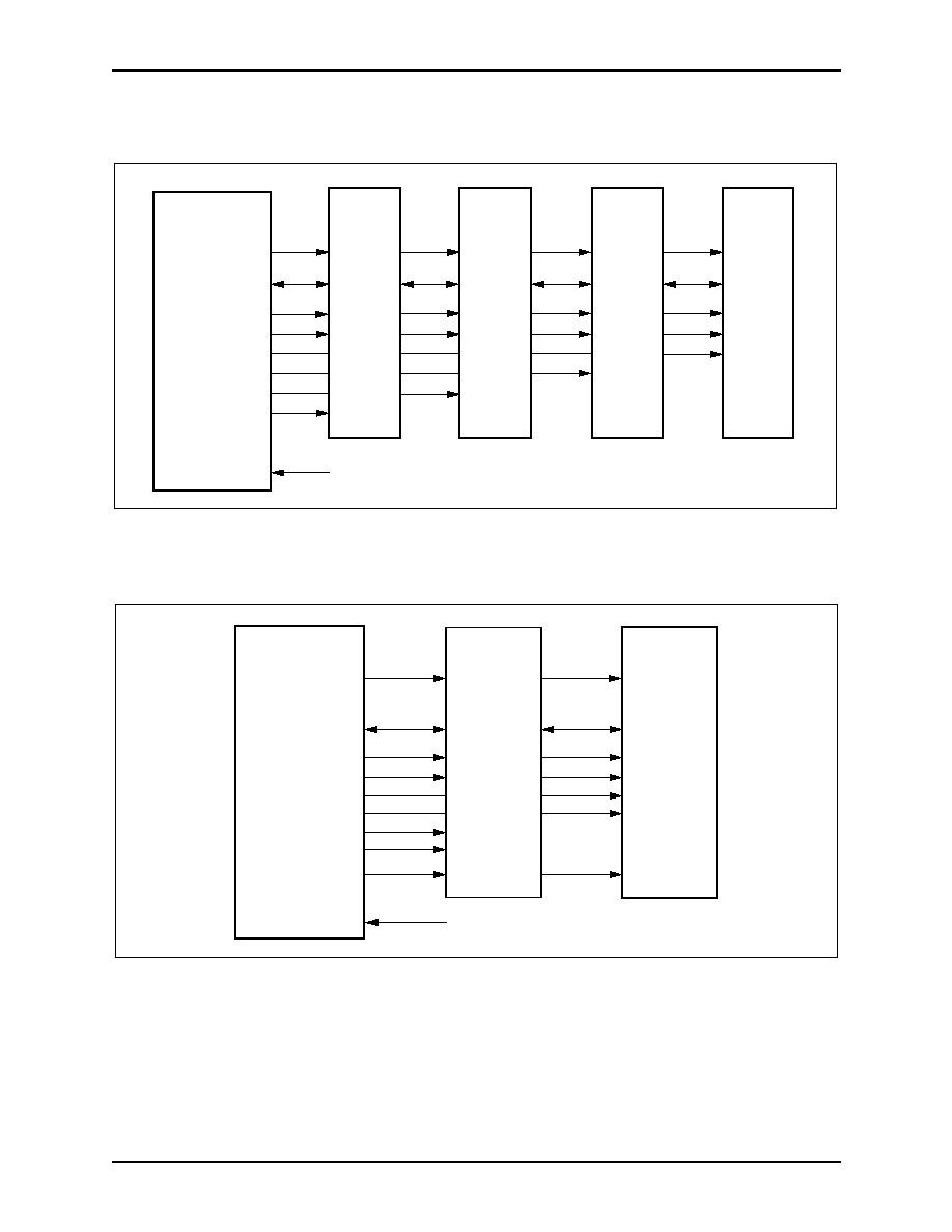
9.0 Local Memory Interface
RS8234
9.2 Memory Bank Characteristics
ATM ServiceSAR Plus with xBR Traffic Management
9-4
Mindspeed Technologies
TM
28234-DSH-001-B
The memory map contains space allocated to the RS825x physical interface
IC, and to a future second Mindspeed PHY device. This mapping is only valid
when the PROCMODE input pin is pulled high, indicating standalone operation
with no local processor present. Standalone operation is detailed in
Section 10.6
.
When PROCMODE is logic low and the local processor is present, addresses
0x100h through 0xFFFh are available for general use and are mapped to
MCS[0]*.
Figure 9-2. 0.5 MB SRAM Bank Utilizing by_8 Devices
LADDR[16:0]
LDATA[31:0]
MCSx*
MOE*
MWE[3]*
MWE[2]*
MWE[1]*
MWE[0]*
MWR*
A[16:0]
D[31:24]
D[23:16]
D[15:8]
D[7:0]
/CS
/OE
/WE
D[7:0]
A[16:0]
/CS
/OE
/WE
D[7:0]
A[16:0]
/CS
/OE
/WE
D[7:0]
A[16:0]
/CS
/OE
/WE
D[7:0]
RS8234
SRAM
SRAM
SRAM
SRAM
RAMMODE
GND
128 k x 8
128 k x 8
128 k x 8
128 k x 8
100074_068
Figure 9-3. 1 MB SRAM Bank Utilizing by_16 Devices
LADDR[17:0]
LDATA[31:0]
MCSx*
MOE*
MWE[3]*
MWE[2]*
MWE[1]*
MWE[0]*
MWR*
A[17:0]
D[31:16]
D[15:0]
/CS
/OE
/WE
D[15:0]
A[17:0]
/CS
/OE
/WE
D[15:0]
RS8234
SRAM
SRAM
/BEH
/BEL
/BEH
/BEL
RAMMODE
Pullup
256 k x 16
256 k x 16
100074_069

RS8234
9.0 Local Memory Interface
ATM ServiceSAR Plus with xBR Traffic Management
9.2 Memory Bank Characteristics
28234-DSH-001-B
Mindspeed Technologies
TM
9-5
The MEMCTRL bit in the CONFIG0 Register selects the number of wait
states that the memory controller uses to access the SRAM. A logic zero indicates
zero wait state or single-cycle memory, while a logic one indicates one wait state
or two-cycle memory. The power-on default is MEMCTRL=1, selecting one wait
state or two-cycle memory accesses.
Accesses made to the control registers and internal SRAM by the local
processor follow the convention for SRAM accesses; that is, either zero or one
wait state, depending on MEMCTRL programming. Subsequently, the local
processor sees no functional timing differences between accesses to registers or
SRAM. The internal register accesses from the PCI slave interface are always
zero wait state. When the RS8234 decodes a PCI slave read to its address space,
the RS8234 performs a prefetch of four subsequent (contiguous) word locations.
SRAM access time requirements are directly proportional to the system clock
speed, as well as the amount and organization of the memory. The required
system clock speed for a given application is dependent on the physical line rate,
number of VCCs, and the percentage of idle cells versus assigned cells. Memory
access times and other requirements are specified at three typical
implementations of one, two, and four banks of by_8 SRAM. In terms of address
bus loading, one bank of by_8 SRAM equals one-half bank of by_16 or two
banks of by_4. In this way, the system designer can choose the appropriate SRAM
characteristics to suit the amount of memory and organization required for the
application. See
Chapter 15.0
for timing information.

9.0 Local Memory Interface
RS8234
9.3 Memory Size Analysis
ATM ServiceSAR Plus with xBR Traffic Management
9-6
Mindspeed Technologies
TM
28234-DSH-001-B
9.3 Memory Size Analysis
Table 9-2
gives the segmentation memory size requirements for 1,024 configured
VCCs under the following assumptions:
SEGMENTATION
1.
Schedule Table is 2,112 schedule slots and each slot is a double word. This
allows CBR and three-priority VBR schedule in 64 K bits/sec increments
for an OC-3 connection.
2.
Eight ABR Templates.
3.
32 OAM PM channels active.
4.
Transmit queues configured for 256 entries.
5.
No status queues in SAR local memory.
6.
Each active channel has an average of one active segmentation buffer.
7.
RS_Queue size is 1,024.
REASSEMBLY
1.
Eight VPIs per 1,024 channels.
2.
1 K preallocation on VPI=0 only.
3.
UNI VPI space.
4.
32 OAM PM channels active.
5.
Free buffer queues configured for 256 entries.
6.
No status queues in SAR local memory.
7.
FBQ pools 0-15 have 4-word entries, and pools 16-31 have 2-word entries.
Table 9-2. Memory Size in Bytes
Data Structure
One Peer
16 Peers
32 Peers
SEG Schedule Table
16,896
16,896
16,896
SEG SEG_PM
1024
1024
1024
RS Queue
8,192
8,192
8,192
SEG Transmit Queues
1,024
16,384
32,768
SEG ER Tables
67,200
67,200
67,200
RSM Free Buffer Queues
4,096
65,536
98,304
RSM PM-OAM
512
512
512
RSM VPI Index Table
1,024
1,024
1,024
Total Fixed
99,200
176,000
225,152
SEG VCC Table
40,960
40,960
40,960
SEG Buffer Descriptors
20,480
20,480
20,480
RSM VCC Table
49,152
49,152
49,152
RSM VCI Index Table
92
92
92
Total Incremental
110,684
110,684
110,684
Grand Total
209,884
286,684
335,836
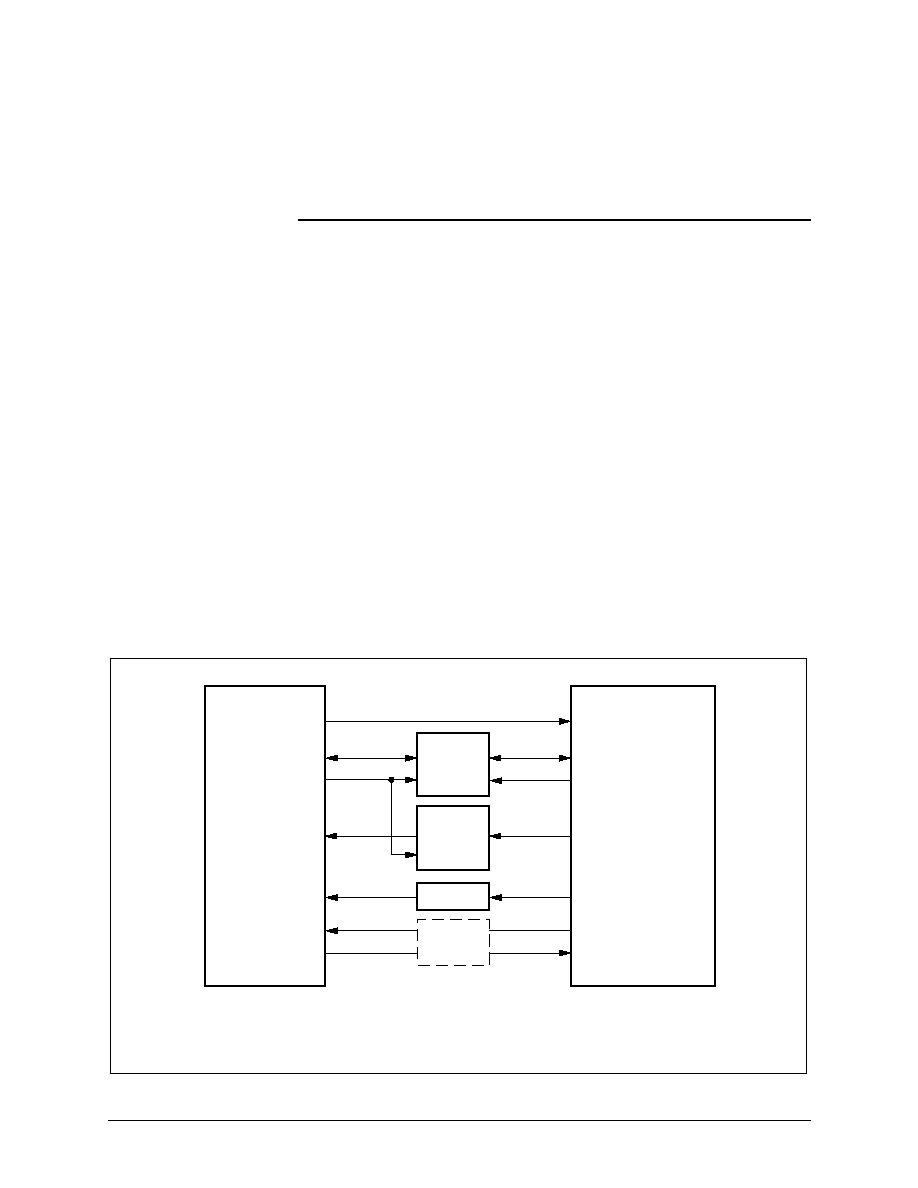
28234-DSH-001-B
Mindspeed Technologies
TM
10-1
10
10.0 Local Processor Interface
10.1 Overview
The RS8234 integrated circuit can be used in conjunction with an external
processor that performs initialization, link management, monitoring, and control
functions. The local processor interface consists of a "loosely coupled"
architecture where it interfaces to the RS8234 through bidirectional transceivers
and buffers that are controlled by the local processor and the RS8234, as shown in
Figure 10-1
. This architecture allows the processor access to all of the RS8234
SAR shared memory and control registers, while insulating the RS8234 from
processor instruction and data cache fills. This also allows the local processor the
option to control multiple RS8234 and/or physical interface devices.
Figure 10-1. RS8234--Local Processor Interface
Dir
Data
Data
Data Enable
Dir
/OE
x32 Xcvr
/OE
Address
Address
x17 Buff
Local Processor
RS8234
High Address
Decode
Chip Select
Control
Status
Control
Status
Optional
Clock
Clock
Logic
(1)
(2)
100074_070
NOTE(S):
(1)
Required to address full 8-MB range. Typically, fewer address lines are used.
(2)
Required for non-i960 processors.

10.0 Local Processor Interface
RS8234
10.1 Overview
ATM ServiceSAR Plus with xBR Traffic Management
10-2
Mindspeed Technologies
TM
28234-DSH-001-B
The processor interface is a generic synchronous interface based on the Intel
i960CA 32-bit architecture and is completely compatible with the i960CA/CF
and the new i960Jx processors. Other synchronous and asynchronous processors
(e.g., from Motorola, AMD, IDT) can be interfaced using external circuitry. The
only requirement is that the processor have a 32-bit bus and that the control
signals be synchronized to SYSCLK.
To access the RS8234 SAR shared memory or control registers, the processor
must arbitrate with the RS8234 for access to the memory controller. Due to the
requirements of reassembly and segmentation access to SRAM, and the
implications of PCI bus utilization, the local processor has the lowest priority in
the memory arbitration scheme. Since the local processor is typically used for low
bandwidth supervision and maintenance functions, this should be acceptable.
When the local processor accesses the RS8234's control registers, internal
SRAM or SAR shared memory, a local processor memory request is generated
internal to the RS8234. The memory arbiter then coordinates this request with
requests from other memory consumers, and grants the memory bus to the local
processor at the appropriate time. The local processor is held off during this
process by the insertion of a variable number of wait states, accomplished by the
i960 withholding READY* or RDYRCV*. Once the local processor is granted
the memory system, the transceivers are enabled to allow the local processor's
address and data to access the SRAM or control registers. The conclusion of the
data transaction is signaled by the assertion of PRDY*. Wait states may be
inserted by the processor at any time by asserting PWAIT*. The last data cycle in
a burst is indicated by the PBLAST* signal. In this manner, non-i960 processor
half-speed buses or slow transceivers can be accounted for.
The LP_BWAIT bit in the CONFIG0 Register will automatically add a single
wait state between the first access in a burst and subsequent accesses. This can be
used to simplify the design of memory controllers for processors that do not
produce a wait output and which require more time between data cycles in a burst.

RS8234
10.0 Local Processor Interface
ATM ServiceSAR Plus with xBR Traffic Management
10.2 Interface Pin Descriptions
28234-DSH-001-B
Mindspeed Technologies
TM
10-3
10.2 Interface Pin Descriptions
The local processor bus interface consists of the control, address, and status
signals described in
Table 10-1
. Refer to
Table 2-1
and
Figure 10-7
,
i80960CA/CF interface description, for further information on these interface
pins.
Table 10-1. Processor Interface Pins
Signal
Dir
(1)
Description
PROCMODE
I
Processor interface mode select input--A logic low on this input enables the local processor mode
of operation.
PCS*
I
Processor interface chip select--A logic low on this signal in conjunction with a logic low on PAS*
at the rising edge of SYSCLK initiates a memory request to the memory controller.
PAS*
I
Processor address strobe-- A logic low on this signal in conjunction with a logic low on PCS*
latches the value of PWNR, PBSEL[1:0], PADDR[1:0], and PBE[3:0]* at the rising edge of SYSCLK.
PWNR
I
Processor write/read select--A logic one on this input indicates a write cycle, a logic zero indicates
a read cycle. Latched at rising edge of SYSCLK when PAS* and PCS* are active.
PADDR[1:0]
I
Word select address inputs--Indicates the word address for a single cycle access, or the first word
for a multi-cycle burst access. Latched at rising edge of SYSCLK when PAS* and PCS* are active.
PBSEL[1:0]
I
Bank select inputs--Decode to select MCS[3:0]*. Latched at rising edge of SYSCLK when PAS*
and PCS* are active.
PBE[3:0]*
I
Byte select inputs--Active low. Allows individual bytes of selected word to be written. Not active on
reads. Latched at rising edge of SYSCLK when PAS* and PCS* active. PBE[3]* controls writes to
LDATA[31:24]; PBE[2]* controls LDATA[23:16]; etc.
PWAIT*
I
Processor wait input--Allows the processor to insert a variable number of wait states to extend
memory transaction. Must be active on rising edge of SYSCLK with PRDY* active to insert wait
cycle. Can be used to interface to half speed or slow processor bus or to allow the use of slow
transceivers. If insertion of wait states is not required, set this input to a logic high. This signal can
only be active, logic low, when PBLAST* is a logic high.
PBLAST*
I
Processor burst last input--Indicates the last word of a cycle. Must be active on rising edge of
SYSCLK with PRDY* active to indicate last cycle. If burst accesses and wait cycles generated by
PWAIT* are not required, this signal should be set to a logic low.
PRDY*
O
Processor interface ready signal--A logic low on this signal at rising edge of SYSCLK indicates
that the present cycle has been completed. If a read cycle, the data is valid to latch by the
processor; if a write cycle, the data has been written and can be removed from the bus. When
PRDY* is active, wait states can be inserted with PWAIT*, or a single or burst cycle can be
terminated by PBLAST*
(2)
.
PFAIL*
I
The local processor can indicate a failure of its internal self-test or initialization processes by
asserting the PFAIL* input to the RS8234.
(1)
Direction given with respect to the RS8234.
(2)
This output corresponds to the READY* or RDYRCV* input in the i960 architecture.
(3)
The processor system is responsible for controlling the direction of the bidirectional data bus transceiver. In the i960
architecture, this can be controlled by the DT/R* signal.

10.0 Local Processor Interface
RS8234
10.3 Bus Cycle Descriptions
ATM ServiceSAR Plus with xBR Traffic Management
10-4
Mindspeed Technologies
TM
28234-DSH-001-B
10.3 Bus Cycle Descriptions
Throughout the bus cycle descriptions, "cycle" refers to a single SYSCLK cycle
ending with a rising edge. An arbitration cycle is one in which the memory
requests from the local processor and internal memory consumers are compared,
and the one with the highest priority is granted the memory access on the next
cycle. A memory access that was previously arbitrated might occur on an
arbitration cycle. Once the local processor has successfully acquired the memory
controller, it holds the bus until it is relinquished by the assertion of PBLAST* on
the last data cycle. Therefore, local processor burst transfers will always be
completed, and can theoretically be of arbitrary length. However, in practice,
burst transfers should be limited to four or less. The maximum arbitration delay
for a local processor access is on the order of 20 cycles; however, it will typically
be from one to four cycles. This parameter is heavily influenced by the SYSCLK
frequency, line rate, number of VCCs, idle cell ratio, and SRAM access speed.
Therefore, a system design in which local processor accesses must occur within a
fixed time period is not recommended.

RS8234
10.0 Local Processor Interface
ATM ServiceSAR Plus with xBR Traffic Management
10.3 Bus Cycle Descriptions
28234-DSH-001-B
Mindspeed Technologies
TM
10-5
10.3.1 Single Read Cycle, Zero Wait State Example
Figure 10-2
illustrates a single read cycle with zero wait states. During the
address cycle (cycle one) at the rising edge of SYSCLK with PCS* and PAS*
active, a memory request is generated by the processor interface circuitry. Also at
this time, the read/write select, bank select, and word select inputs (PWNR,
PBSEL[1:0], and PADDR[1:0]) are internally latched. The byte enables
(PBE[3:0]*) are Don't-Cares during reads. During cycle two, this local processor
memory request is processed by the memory arbitration circuitry. If no other
memory consumers request an access on the same cycle, the local processor is
granted access on cycle three. However, to take into account bus transceiver
turnaround, cycle three is always a wait or bus recovery state, which gives
sufficient time for the address from the processor to access the SRAM. For zero
wait state SRAM, unless a wait state is inserted by the processor, the data is
available to be latched into the processor on cycle four, which is indicated by the
assertion of PRDY*. Cycle five is an arbitration cycle for the internal memory
consumers, which might have requested access during the processor access. It
also serves as a bus recovery cycle for the processor. Once the PCS*, PAS*,
PWNR, PBSEL[1:0], and PADDR[1:0] are sampled at cycle one, they are
Don't-Cares for the remainder of the access. DT/R* is an output supplied by the
local processor to indicate the direction of the data transceivers. The RS8234
PDAEN* signal is active to enable data and address.
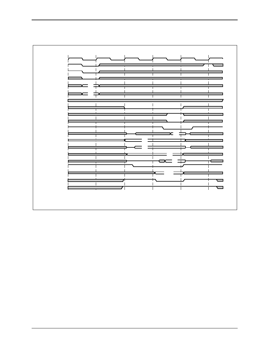
10.0 Local Processor Interface
RS8234
10.3 Bus Cycle Descriptions
ATM ServiceSAR Plus with xBR Traffic Management
10-6
Mindspeed Technologies
TM
28234-DSH-001-B
Figure 10-2. Local Processor Single Read Cycle
ta
tarb
tbr
td
tbr/tabr
SYSCLK
PCS*
PAS*
PWNR
PBSEL[1:0]
PADDR[1:0]
PBE[3:0]
DT/R*
PWAIT*
PBLAST*
PRDY*
D[31:0]
A[20:4]
LADDR[18:2]
LADDR[1:0]
LDATA[31:0]
PDAEN*
MCS*[3:0]
MOE*
MWE*[3:0]
0111
D0
10
A0
A0
D0
11
10
Address
Cycle
1.
Arbitration
Cycle
2.
Bus
Recovery
Cycle
3.
4. Data Cycle
5. Bus Recovery
Next Arbitration
Cycle
100074_071
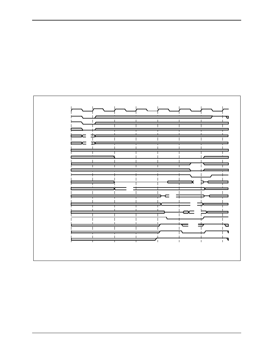
RS8234
10.0 Local Processor Interface
ATM ServiceSAR Plus with xBR Traffic Management
10.3 Bus Cycle Descriptions
28234-DSH-001-B
Mindspeed Technologies
TM
10-7
10.3.2 Single Read Cycle, Wait States Inserted By Memory Arbitration
Figure 10-3
illustrates a local processor single read cycle with arbitration wait
states. This example is similar to the preceding one, except that here the local
processor is not able to access the RAM immediately because of higher priority
memory requests on cycles two and three. On cycle four, the memory controller
allows the local processor access to the address and data bus and the transaction
takes place at the end of cycle six.
Figure 10-3. Local Processor Single Read Cycle with Arbitration Wait States
1
2
3
4
5
6
7
SYSCLK
PCS*
PAS*
PWNR
PBSEL[1:0]
PADDR[1:0]
PBE[3:0]
DT/R*
PWAIT*
PBLAST*
PRDY*
D[31:0]
A[20:4]
LADDR[18:2]
LADDR[1:0]
LDATA[31:0]
PDAEN*
MCS*[3:0]
MOE*
MWE*[3:0]
ta
tarb
tbr
td
tarb
tarb
tarb
11
10
A0
D0
A0
10
D0
0111
Address
Cycle
1.
Arbitration
Cycle
2.
Arbitration
Cycle
3.
Arbitration
Cycle
7.
Arbitration
Cycle
4.
Bus
Recovery
Cycle
5.
6. Data
Cycle
100074_072

10.0 Local Processor Interface
RS8234
10.3 Bus Cycle Descriptions
ATM ServiceSAR Plus with xBR Traffic Management
10-8
Mindspeed Technologies
TM
28234-DSH-001-B
10.3.3 Double Read Burst With Processor Wait States
In
Figure 10-4
the processor inserts wait states on cycle four and cycle six, to
allow additional time for the reads to occur. At the rising edge of SYSCLK on
cycle four and cycle six, the combination of PWAIT* low and PRDY* low
extends the read by one more cycle. The local processor word select inputs
(PADDR[1:0]) are latched at cycle one. The RS8234 word select address lines,
LADDR[1:0], are incremented automatically at the beginning of cycle six.
Figure 10-4. Local Processor Double Read with Wait States Inserted
SYSCLK
PCS*
PAS*
PWNR
PBSEL[1:0]
PADDR[1:0]
PBE[3:0]
DT/R*
PWAIT*
PBLAST*
PRDY*
D[31:0]
A[20:4]
LADDR[18:2]
LADDR[1:0]
LDATA[31:0]
PDAEN*
MCS*[3:0]
MOE*
MWE*[3:0]
ta
tarb
tbr
tw
td
td
tw
D0
D1
1101
10
00
A0
A0
00
D0
01
D1
Address
Cycle
1.
Arbitration
Cycle
2.
Bus
Recovery
Cycle
3.
Data
Cycle
7.
Wait
Cycle
4.
Data
Cycle
5.
6. Wait
Cycle
2
3
4
5
6
7
1
100074_073
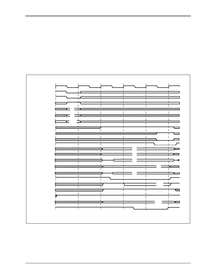
RS8234
10.0 Local Processor Interface
ATM ServiceSAR Plus with xBR Traffic Management
10.3 Bus Cycle Descriptions
28234-DSH-001-B
Mindspeed Technologies
TM
10-9
10.3.4 Single Write With One-Wait-State Memory
In
Figure 10-5
, the local processor performs a single write into one-wait-state
memory. There is no arbitration delay. RAMMODE is a logic high, indicating that
by_16 RAM is used. Here the PBE[3:0]* inputs are latched at cycle one, and are
used to select the byte enables that are active during the cycle when MWR* is
active. In this case, the two most significant bits are active, indicating a 16-bit
write to the two most significant bytes.
Figure 10-5. Local Processor Single Write with One Wait State by_16 SRAM
1
2
3
4
5
SYSCLK
PCS*
PAS*
PWNR
PBSEL[1:0]
PADDR[1:0]
PBE*[3:0]
DT/R*
PWAIT*
PBLAST*
PRDY*
D[31:0]
A[20:4]
LADDR[18:2]
LADDR[1:0]
LDATA[31:0]
PDAEN*
MCS*[3:0]
MOE*
RAMMODE
MWE*[3:0]
MWR*
ta
tarb
tbr
tw
td
D0
1110
0011
D0
A0
A0
01
00
01
0011
Address
Cycle
1.
Arbitration
Cycle
2.
Bus
Recovery
Cycle
3.
Wait
Cycle
4.
Data
Cycle
5.
100074_074
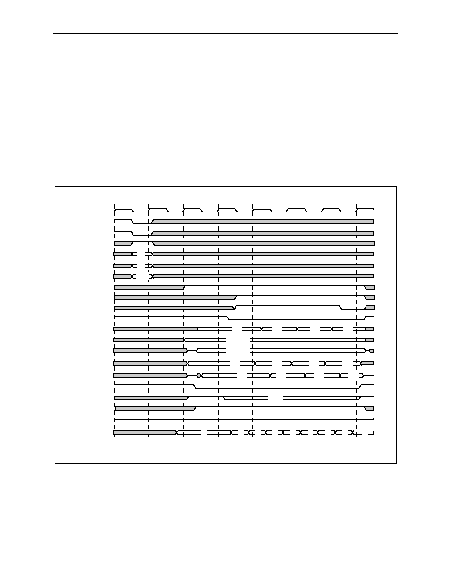
10.0 Local Processor Interface
RS8234
10.3 Bus Cycle Descriptions
ATM ServiceSAR Plus with xBR Traffic Management
10-10
Mindspeed Technologies
TM
28234-DSH-001-B
10.3.5 Quad Write Burst, No Wait States
In
Figure 10-6
, a quad burst write access to zero-wait-state memory is shown.
RAMMODE is logic low, selecting by_8 or by_4 RAM mode. Here PBE[3:0]* is
latched on cycle one, indicating that the write is active on all bytes, and the
MWE*[3:0] outputs are active as write strobes while MWR* is not used. The
SAR shared memory word select addresses, LADDR[1:0], are incremented
automatically by the RS8234 on each successive write cycle. Although the i960
architecture has the limitation that a quad word transfer must start on a quad word
boundary, the RS8234 does not have that limitation. Thus, the PADDR[1:0] bits
can be any value and are incremented as long as the burst transfer proceeds.
Figure 10-6. Local Processor Quad Write, No Wait States
1
2
3
4
5
6
7
SYSCLK
PCS*
PAS*
PWNR
PBSEL[1:0]
PADDR[1:0]
PBE[3:0]
DT/R*
PWAIT*
PBLAST*
PRDY*
D[31:0]
A[20:4]
LADDR[18:2]
LADDR[1:0]
LDATA[31:0]
PDAEN*
MCS*[3:0]
MOE*
RAMMODE
MWE*[3:0]
ta
tarb
tbr
td
td
td
td
D0
D1
D2
D3
Address
Address
00
01
10
11
D0
D1
D2
D3
1011
F
0
F
0
F
0
F
0
F
01
00
0000
Address
Cycle
1.
Arbitration
Cycle
2.
Bus
Recovery
Cycle
3.
Data3
Cycle
7.
Data
Cycle
4.
Data1
Cycle
5.
6. Data2
Cycle
100074_075
RS8234
10.0 Local Processor Interface
ATM ServiceSAR Plus with xBR Traffic Management
10.4 Processor Interface Signals
28234-DSH-001-B
Mindspeed Technologies
TM
10-11
10.4 Processor Interface Signals
Figure 10-7
illustrates the signal interface between the RS8234 device and the
i960CA/CF processor. The memory region decoded for PCS* should be set for
N
RAD
and N
WAD
= 2, N
RDD
and N
WDD
= 0 or 1 (depending on the use of zero or
one wait state SRAM), and N
XDA
= 1. In addition, external ready control must be
enabled, and burst can be enabled or disabled at the system designer's option.
Pulling up the i960 CLKMODE input to a logic one selects the divide-by-one
clock mode, making i960 PCLK synchronous to SYSCLK.
Figure 10-7. i960CA/CF to the RS8234 Interface
i960CA/CF
A[2]
A[3]
SRAM
A[20:4]
A[1]
A[0]
A[18:2]
PADDR[0]
PADDR[1]
LADDR[18:2]
LADDR[1]
LADDR[0]
D[31:0]
LDATA[31:0]
D[31:0]
A[22:21]
PBSEL[1:0]
READY*
BE[3:0]*
BLAST*
PRDY*
PBE[3:0]*
PBLAST*
WAIT*
PWAIT*
W/R*
PWNR
RESET*
XINT0
FAIL*
AS*
CLKIN
PRST*
PINT*
PFAIL*
PAS*
SYSCLK
WE[3:0]
MWE[3:0]*
MOE*
OE
SRAMCS*
SRAMCS*
SRAMCS*
SRAMCS*
MCS[3]*
MCS[2]*
MCS[1]*
MCS[0]*
DT/R*
PCS*
Decode
x32 Xcvr
x17 Buff
(1)
PDAEN*
MWR*
For by_16 SRAM
A[31:28]
CLKMODE
Pullup
PROCMODE
GND
RAMMODE
GND for by_8 or by_4,
VCC for by_16
PCLK
NC
RS8234
100074_076
NOTE(S):
(1)
Required for full 8 MB address range.

10.0 Local Processor Interface
RS8234
10.5 Local Processor Operating Mode
ATM ServiceSAR Plus with xBR Traffic Management
10-12
Mindspeed Technologies
TM
28234-DSH-001-B
This configuration is for addressing the entire 8 MB of SRAM. In the majority
of systems, the SRAM requirements will be considerably less. The implications
of this are that the PBSEL[1:0] inputs can be driven by lower order address lines,
and there will be less than 17 address lines to buffer. Therefore, in most
applications, the data transceivers can utilize two x_16 parts, such as a
74ABT16245, and the address buffer can utilize a single x_16 74ABT16244.
NOTE:
The i960CA/CF signals a failure of its internal self-test upon reset or
power-up, by asserting its FAIL* output. This line is connected to the
PFAIL* pin of the RS8234, and the status of this pin is reflected in the
Host Interrupt Status Register [HOST_ISTAT0; 0xC0].
10.5 Local Processor Operating Mode
The major difference between the i80960Jx processor and the i80960CA is that
the i80960Jx utilizes a multiplexed address/data bus structure, while the
i80960CA/CF is non-multiplexed. However, in the RS8234 system, the
demultiplexing of address/data takes place on the processor side of the address
buffers and, therefore, does not affect the RS8234. Otherwise, the i80960Jx has
the same bus control signals as the i80960CA/CF with the exception of the
WAIT* signal, which the i80960Jx does not possess. The insertion of wait states,
if required, must be accomplished by an external memory controller, which in any
case, is required for a i80960Jx implementation.

RS8234
10.0 Local Processor Interface
ATM ServiceSAR Plus with xBR Traffic Management
10.6 Standalone Operation
28234-DSH-001-B
Mindspeed Technologies
TM
10-13
10.6 Standalone Operation
Standalone interface pins and descriptions are given in
Table 10-2
.
Figure 10-8
shows the signal interface between the RS8234 and the RS825x ATM
receiver/transmitter device with no local processor. The PCS*, PAS*, and PWNR
pins are now outputs providing chip select, address strobe, and write/read control
to the RS825x. PDAEN* is now an input connected to the interrupt sources of the
RS825x. PBLAST* is a second chip select, which can be used to connect a future
second Mindspeed PHY device. The PRDY* output is active and indicates the
cycles in which the data transaction occurs. The PWAIT* input is active and can
be used to prolong the cycle as shown in
Figure 10-9
. Physical interface devices
other than the RS825x can be connected by using PWAIT* to extend the read or
write cycle, and by using external logic to translate the RS8234 control signals.
Table 10-2. Standalone Interface Pins
Signal
Dir
(1)
Description
PROCMODE
I
Processor interface mode select input. A logic one enables standalone operation without a
local processor.
PCS*
O
Chip select output for PHY device number one. Synchronous to SYSCLK.
PBLAST*
O
Chip select output for PHY device number two. Synchronous to SYSCLK.
PAS*
O
PHY address strobe. Synchronous to SYSCLK.
PWNR
O
PHY write/read select. A logic one on this output indicates a write cycle, a logic zero
indicates a read cycle. Synchronous to SYSCLK.
PRDY*
O
PHY interface ready signal. A logic low on this signal at rising edge of SYSCLK indicates
that the data cycle has been completed.
PWAIT*
I
PHY wait input. Allows external logic to insert wait states to extend data cycles. Only
active when PRDY* is active.
PDAEN*
I
PHY interrupt input, active low, level sensitive
(2)
.
PADDR[1:0]
I
Not used, pull to logic zero.
PBSEL[1:0]
I
Not used, pull to logic zero.
PBE[3:0]*
I
Not used, pull to logic zero.
PFAIL*
I
Not used, pull to logic one.
NOTE(S):
(1)
Direction given with respect to the RS8234.
(2)
See the HOST_ISTAT0 Register for details.
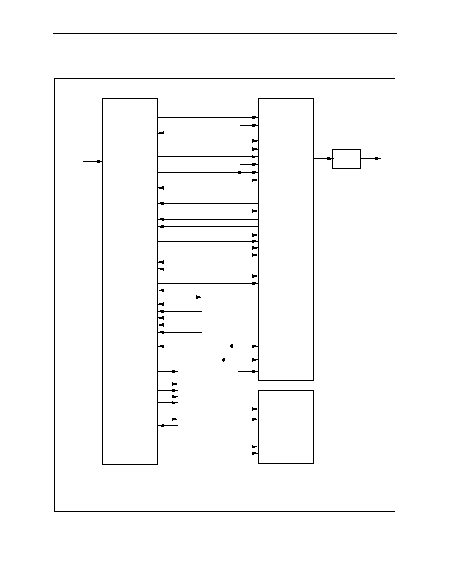
10.0 Local Processor Interface
RS8234
10.6 Standalone Operation
ATM ServiceSAR Plus with xBR Traffic Management
10-14
Mindspeed Technologies
TM
28234-DSH-001-B
Figure 10-8. RS825x and SAR (RS8234) Interface (Standalone Operation)
CN825x
RS8234 SAR
SRAM
PADDR[0]
PADDR[1]
Data[7:0]
LDATA[31:0]
PBSEL[1:0]
Cs*
W/R*, Rd*
As*, Wr*
PRDY*
PBE[3:0]*
PBLAST*
Mclk, ClkSel
PWAIT*
PWNR
PRST*
PDAEN*
PFAIL*
PAS*
SYSCLK
A[18:0]
D[31:0]
LADDR[18:0]
Addr[6:0]
SRAMCS*
SRAMCS*
SRAMCS*
Int*
WE[3:0]*
MWR[3:0]*
OE*
MOE*
SRAMCS*
MCS[3]*
MCS[2]*
MCS[1]*
MCS[0]*
Reset*
PCS*
Pullup
N/C
(2)
GND
GND
GND
GND
Open
Pullup
PROCMODE
MWR*
For x16 SRAM
RAMMODE
GND for x_8 or x_4
Pullup for x_16
Pullup
Pullup
(1)
SyncMode
Fiber
PMD
or
Cat 5
PCI
Bus
Device
TxData[7:0]
TxData[15:8]
TxClav
TxEnb*
TxSOC
TxPrty
TxAddr[4:0]
UtopTxClk
UtopRxClk
RxData[7:0]
RxData[15:8]
RxClav
RxEnb*
RxSOC
RxPrty
RxAddr[4:0]
TXD[7:0]
TXCLAV
TXEN
TXSOC
TXPAR
CLKD3
RXD[7:0]
RXCLAV
RXEN*
RXSOC
RXPAR
GND
GND
Open
GND
VCC
100074_077
NOTE(S):
(1)
Can be driven by external circuitry to extend cycles.
(2)
Can be used by external circuitry.

RS8234
10.0 Local Processor Interface
ATM ServiceSAR Plus with xBR Traffic Management
10.6 Standalone Operation
28234-DSH-001-B
Mindspeed Technologies
TM
10-15
Figure 10-9. RS8234/PHY Functional Timing with Inserted Wait States
ta
tw
tw
td
Write Address
Write Data
1
2
3
4
5
SYSCLK
PCS*
PAS*
PWNR
PWAIT*
PRDY*
LADDR[13:0]
LDATA[7:0]
100074_078
10.0 Local Processor Interface
RS8234
10.6 Standalone Operation
ATM ServiceSAR Plus with xBR Traffic Management
10-16
Mindspeed Technologies
TM
28234-DSH-001-B
Figure 10-10
shows a read and write RS825x access. At cycle one (the rising
edge of SYSCLK) the RS825x samples PCS*, PAS*, and PWNR low, indicating
a read cycle. By the next rising edge of SYSCLK at cycle two, the data is output
by the RS825x to be latched by the RS8234. The same procedure occurs for a
write except that at cycle four, PWNR is sampled high. The RS825x then latches
the data to the appropriate internal register on the next SYSCLK rising edge at
cycle five.
Figure 10-10. RS8234/RS825x Read/Write Functional Timing
tA
tD
tA
tD
Read Address
Write Address
Read Data
Write Data
1
2
3
4
5
6
SYSCLK
PCS*
PAS*
PWNR
PWAIT*
PRDY*
LADDR[13:0]
LDATA[7:0]
1, 2 Read Cycle
4, 5 Write Cycle
100074_079

RS8234
10.0 Local Processor Interface
ATM ServiceSAR Plus with xBR Traffic Management
10.7 System Clocking
28234-DSH-001-B
Mindspeed Technologies
TM
10-17
10.7 System Clocking
The RS8234 derives all of its timing from a 2x clock input, CLK2X. This clock is
internally divided by two to create the system clock, SYSCLK. This system clock
is used internal to the device, and is output to the system to provide the clock to
an external processor or PHY device. All processor interface signals are
synchronous to SYSCLK.
In addition, CLKD3 (CLK2X asymmetrically divided by three, an output
clock), is provided, and can be used as the clock for the UTOPIA ATM physical
interface. The clock signal would be looped externally to RXCLK (aka
FRCTRL). For example, if CLK2X is 66 MHz, then CLKD3 is 22 MHz, and is
suitable for the UTOPIA interface. If CLK2X is 50 MHz, then SYSCLK is 25
MHz and is suitable for the UTOPIA interface.
The CLK2X frequency required for a given application is a function of the
physical line rate, number of VCCs, active concurrent VCCs, and the SRAM
cycle time.
10.8 Real-Time Clock Alarm
A real-time clock counter and alarm registers are built into the RS8234. This
real-time clock consists simply of a 7-bit prescaler (configured via the DIVIDER
field in the CONFIG0 Register) that accepts the SYSCLK input and outputs a
constant (nominally 1 MHz) pulse train, and a 32-bit read/write counter (the
Real-Time Clock Register [CLOCK;0x00]), that counts the number of pulses
output by the prescaler since the system was initialized. When the prescaler is set
to generate a 1 MHz pulse train, the CLOCK counter counts in 1
�
s intervals. An
interrupt is generated when the CLOCK counter overflows, i.e., more than 2
32
pulses have occurred since it was cleared to zero. If this happens, the CLOCK
counter simply wraps around to zero and starts counting over. The control
processor or host software is responsible for noting the overflow.
One simple real-time alarm is implemented in the RS8234. This is Alarm
Register 1 [ALARM1;0x04], which is continuously compared to the Clock
Register. When a match is detected, the corresponding interrupt is generated to
the local or host processors. Either processor can then respond to this interrupt
and reload a new value into the ALARM1 Register.

10.0 Local Processor Interface
RS8234
10.9 RS8234 Reset
ATM ServiceSAR Plus with xBR Traffic Management
10-18
Mindspeed Technologies
TM
28234-DSH-001-B
10.9 RS8234 Reset
The RS8234 must be reset by the host processor prior to system initialization for
proper operation. This can be done in one of two ways: by asserting the external
HRST* pin (which is normally connected to the system power-up reset circuitry),
or by setting the GLOBAL_RESET bit in the Configuration Register 0
[CONFIG0;0x14]. The HRST* pin must be deasserted and GLOBAL_RESET
must be cleared before beginning the RS8234 initialization process.
Asserting the HRST* input pin automatically causes the local processor reset
pin to be driven active. The reset to the local processor will stay active until the
LP_ENABLE bit in the CONFIG0 Register is set to a logic high. When using the
GLOBAL_RESET bit, the processor must manually set or clear the appropriate
bits in the CONFIG0 Register.

28234-DSH-001-B
Mindspeed Technologies
TM
11-1
11
11.0 PCI Bus Interface
11.1 Overview
The PCI bus interface is compliant with PCI Local Bus Specification,
Revision 2.1. With the exception of HRST* and HINT*, this interface is
completely synchronous to the PCI bus clock (HCLK). All inputs are sampled at
the rising edge of HCLK, and all outputs are driven by the RS8234 to be valid
before the next rising edge of HCLK.
The maximum PCI bus clock rate supported by the RS8234 is 33 MHz. The
PCI bus interface logic is clocked directly from the PCI bus clock, while the
remainder of the RS8234 logic runs off separate clocks. Synchronizing registers
and FIFOs are implemented in the PCI bus interface in order to transfer data
between the PCI bus clock (HCLK) and the system (SYSCLK) clock domains.
The PCI bus drivers are shared between master and slave bus interface
functional blocks. The PCI bus master logic (within the device) arbitrates via the
PCI bus arbiter (external to the device) for access to the PCI bus; access to the
PCI bus automatically implies access to the bus drivers, since no other master can
be concurrently communicating with the slave logic. The bus master logic
contends for the bus on a transaction by transaction basis.
The PCI bus interface responds to read and write requests by the host CPU,
allowing access to chip resources by host software. The RS8234 is also capable of
acting as DMA bus master on the PCI bus. As a result, the PCI bus interface
implements the full set of address, data, and control signals required to drive the
bus as master, and contains the logic required to support arbitration for the PCI
bus. The DMA coprocessor and the PCI bus interface are closely linked and,
hence, are shown as one unit.

11.0 PCI Bus Interface
RS8234
11.1 Overview
ATM ServiceSAR Plus with xBR Traffic Management
11-2
Mindspeed Technologies
TM
28234-DSH-001-B
The PCI bus interface functional blocks are as follows:
�
I/O drivers and receivers that drive the pins connected to the PCI bus
signals.
�
PCI bus master logic that allows the bus interface to acquire mastership of
the PCI bus and act as a transaction initiator. The bus master logic also
contains a command decoder that interprets access commands generated
by the DMA coprocessor, and a burst controller for controlling the
duration of each read or write burst. In addition, the bus master logic
contains address counters that allow it to restart and retry burst transfers if
required by the transaction target.
�
Burst FIFO buffers that store and transfer bursts of data words between the
DMA coprocessor and the PCI bus master logic.
�
PCI bus slave logic that responds to transactions initiated by other masters
on the PCI bus with the RS8234 as a target. The bus slave logic also
synchronizes data passed back and forth across the clock boundary
between the PCI bus interface and the internal chip logic.
�
Configuration registers holding initialization parameters and PCI bus
status information.
�
Logic that allows the host CPU to read/write the internal RS8234 registers
via the PCI slave port.
�
Logic to enable read/write access to the SAR shared memory space from
the host CPU, again via the PCI slave port.
�
An Interface module that allows the PCI core to connect to a serial
EEPROM.

RS8234
11.0 PCI Bus Interface
ATM ServiceSAR Plus with xBR Traffic Management
11.2 Unimplemented PCI Bus Interface Functions
28234-DSH-001-B
Mindspeed Technologies
TM
11-3
11.2 Unimplemented PCI Bus Interface
Functions
The PCI bus interface on the RS8234 does not implement all the transaction types
defined by the PCI bus specification; only those sections of the protocol that are
necessary for slave and DMA memory accesses are implemented. In particular,
the following transaction types are not implemented:
�
64-bit transfers, as well as the Dual Address Cycle command.
�
Snooping and cache support. Memory Read Line, Memory Write and
Invalidate commands are internally aliased to the Memory Read and
Memory Write commands as per the PCI specification.
�
Locked and exclusive accesses: the PCI LOCK* line is not driven by the
RS8234, and the PCI slave interface does not handle locked accesses by
other bus masters in any special manner.
�
I/O accesses (the I/O Read and I/O Write commands).
�
Interrupt acknowledge cycles, including the Interrupt Acknowledge
command.
�
The Special Cycle command and Special Cycle transactions.
�
Burst transfers that do not have simple, sequentially incrementing
addresses for consecutive data phases. The PCI master logic always
performs sequentially incrementing burst transfers. The two LSBs of the
PCI address lines (AD[1,0]) must be zero during the address phase of any
transfer made to the PCI slave logic (indicating sequentially incrementing
burst addresses). If AD[1,0] is not equal to zero, the slave logic will signal
a type A or B target disconnect after the first data phase, forcing the
external master to perform a single word transfer as per the PCI
specification.
11.3 PCI Configuration Space
In accordance with the PCI bus specification Revision 2.1, the RS8234 PCI bus
interface implements a 128-byte configuration register space. These
configuration registers can be used by the host processor to initialize, control, and
monitor the SAR bus interface logic. The complete definitions of these registers
and the relevant fields within them is given in the PCI bus specification, and will
not be repeated here. The descriptions and definitions of these register fields as
implemented in the RS8234 is shown in
Chapter 13.0
.

11.0 PCI Bus Interface
RS8234
11.4 PCI Bus Master Logic
ATM ServiceSAR Plus with xBR Traffic Management
11-4
Mindspeed Technologies
TM
28234-DSH-001-B
11.4 PCI Bus Master Logic
The PCI bus master logic block is responsible for accepting read and write
commands from the DMA coprocessor (passed via the burst FIFO buffers), and in
turn acquiring mastership of the PCI bus and generating transactions to perform
the actual data transfers. The bus master logic contains the following:
�
A command decoder that interprets commands issued from the DMA
coprocessor.
�
A burst controller that counts off read and write cycles in each burst on the
PCI bus (and also latches and drives the address and command during the
address phase of each transfer).
�
Arbitration logic that acquires control of the PCI bus.
�
Arbitration parking.
�
A bus state machine that sequences and controls transfers.
It is possible for the addressed slave to request a disconnect or a retry during a
read or a write transfer, using the defined PCI protocol sequence. In this case, the
bus master logic will terminate the current burst, maintain its bus request, and
restart the transfer at the point of termination. Disconnects and retries are not
regarded as errors.
Five possible sources of error are present during any PCI bus master
transaction. If any of the following five errors occur, the bus master logic will
permanently terminate the transaction, flag an error, and cease to process any
more commands.
1.
Target Abort--The PCI transaction will terminate if the addressed target
signals a target abort. In this case, the RTA and MERROR bits in the PCI
Configuration Register space will be set and the PCI_BUS_STATUS[4] bit
in the SYS_STAT Register will be set.
2.
Master Abort--If the addressed target does not respond with an
HDEVSEL* assertion, then a master abort is flagged. In this case, the
RMA and MERROR bits in the PCI Configuration Register space will be
set and the PCI_BUS_STATUS[3] bit in the SYS_STAT Register will be
set.
3.
Parity Error--If the data parity checked during read transfers is
inconsistent with the state of the HPAR signal, then a parity error is
signaled. In this case, the DPR and MERROR bits in the PCI
Configuration Register space will be set and the PCI_BUS_STATUS[2] bit
in the SYS_STAT Register will be set.

RS8234
11.0 PCI Bus Interface
ATM ServiceSAR Plus with xBR Traffic Management
11.5 Burst FIFO Buffers
28234-DSH-001-B
Mindspeed Technologies
TM
11-5
4.
Interface Disabled--If the driver or application software on the PCI host
CPU has disabled, the RS8234 PCI bus master logic (using the M_EN bit
in the Command field of the PCI bus configuration registers), then any
attempt to perform a DMA transaction to the PCI bus will result in an
error. In this case, the MERROR and INTF_DIS bits in the PCI
configuration space will be set and the PCI_BUS_STATUS[1] bit in the
SYS_STAT Register will be set.
5.
Internal Failure--Upon a synchronization error between the DMA
coprocessor and the PCI master logic, an internal failure will be flagged. In
this case, the MERROR and INT_FAIL bits in the PCI configuration space
will be set and the PCI_BUS_STATUS[0] bit in the SYS_STAT Register
will be set.
NOTE:
The above errors permanently affect system level operation. Because of
this the system should be re-initialized, since full system level recovery is
unlikely. The bus protocol errors can be cleared either by a software reset
of the associated status flag or flags, i.e., RTA, RMA, or DPR, or with a
reset of the PCI bus master logic using the HRST* input pin. For example,
a master abort error can be cleared by writing a logic one to the RMA
status bit in the PCI Configuration Register space, causing the status bit to
be cleared. Internal failures (attempting to initiate a master transaction
with the interface disabled, or loss of synchronization with the DMA
controller) can only be reset by applying the global reset, CONFIG0
(GLOBAL_RESET), or by asserting the HRST* signal.
Next, the MERROR bit must be cleared. The MERROR bit in the PCI
Configuration Register drives the PCI_BUS_ERROR interrupt. To clear
this interrupt, a logic high must be written to the MERROR bit location.
The MERROR bit can also be cleared by a logic low on the HRST* input
pin.
The local processor can clear the error bits by setting CONFIG0
(PCI_ERR_RESET) to a logic high. After the errors have been cleared, the
SAR should be re-initialized.
Several fields are provided in the PCI configuration space to aid in
recovering from a PCI master error. The PCI host software can determine
that an error occurred by checking the MERROR bit. It can also determine
if the transaction was a read or write by inspecting the MRD bit, and then
retrieve the read or write address at which an error occurred by reading the
MASTER_READ_ADDR or MASTER_WRITE_ADDR fields.
The PCI Read and PCI Read MULTIPLE commands issued by the PCI
block are under the control of the PCI_READ_MULTI bit in the
CONFIG0 register.
11.5 Burst FIFO Buffers
Two small FIFO buffers are implemented to support PCI burst-mode operation, to
allow synchronization between the RS8234 internal logic and the PCI bus
interface, and to carry commands from the DMA coprocessor to the PCI bus
logic. The incoming FIFO is 512 x 32 bits, the outgoing FIFO is 16 x 36 bits.

11.0 PCI Bus Interface
RS8234
11.6 PCI Bus Slave Logic
ATM ServiceSAR Plus with xBR Traffic Management
11-6
Mindspeed Technologies
TM
28234-DSH-001-B
11.6 PCI Bus Slave Logic
The PCI slave logic permits the host CPU on the PCI bus to access and modify
RS8234 resources (the external SAR shared memory, internal memory, and
internal registers). Because the control processor also has access to these
resources, the PCI slave logic must arbitrate for access prior to performing any
read or write transaction. The slave logic also contains the PCI configuration
registers. These registers control the PCI slave and master interfaces, and can be
read or written at any time by the PCI host. The slave logic implements the
synchronizers required for rate-matching between the PCI bus clock and the
internal RS8234 system clock. Also, small FIFOs are used to speed up burst reads
(8x32) and writes (64x32) performed by the host processor to local resources, by
buffering prefetched read data and absorbing latency during consecutive writes.
In general, the PCI slave interface functions as a normal memory-mapped PCI
target, responding to Memory Read, Memory Write, Configuration Read, and
Configuration Write commands from any initiator on the PCI bus. The slave
interface will respond only to Memory Read and Memory Write commands if the
MS_EN bit of the Command field in the PCI Configuration Register has been set.
The PCI slave logic does not implement special cycle commands, or respond
to special cycles on the PCI bus. If a master performs a special cycle on the PCI
bus, the following occurs:
�
The slave logic never asserts HDEVSEL*.
�
Parity errors during the address phase of the special cycle command will
be reported to be asserting HSERR* in the normal fashion, if SE_EN and
PE_EN in the command register are both set.
�
Parity errors during the data phase are ignored.
11.7 Byte Swapping of Control Structures
Two control bits in the PCI configuration space are used to configure byte
swapping, in order to align with various big and little endian host system
requirements.
The SLAVE_SWAP control bit is bit 29 of address offset 0x40 in the PCI
Configuration register. When SLAVE_SWAP is set to a logic high, the slave
interface swaps the bytes of a slave write or read access. The default setting for
this bit is logic low.
The MSTR_CTRL_SWAP control bit is bit 30 of address offset 0x40 in the
PCI Configuration register. When MSTR_CTRL_SWAP is set to a logic high, the
control structures that the SAR writes are written with bytes swapped. The default
setting for this bit is logic low.
The HRST* pin made active will cause both of these bits to be logic low.

RS8234
11.0 PCI Bus Interface
ATM ServiceSAR Plus with xBR Traffic Management
11.8 Power Management
28234-DSH-001-B
Mindspeed Technologies
TM
11-7
11.8 Power Management
Power Management, as a defined class of functions, consists of mechanisms in
software and hardware to minimize system power consumption, manage system
thermal limits, and maximize system battery life. The RS8234 supports Power
Management on the PCI bus according to the PCI Bus Power Management
Interface Specification, Revision 1.0.
Power management states are defined as varying, distinct levels of power
savings. The RS8234 device supports the two mandatory power states,
D0
and
D3
, of the PCI Bus Power Management Interface Specification.
D0
is the
maximum powered state (on) and
D3
is the minimum powered state (off). When
in the
D3
state, SYSCLK is turned off.
Refer to
Section 13.7
for the detailed information on the PCI Configuration
space and PCI registers concerned with implementing the Power Management
functions.
Power Management is enabled by default. This capability can be disabled via
bit 2 of the EEPROM (Disable Capability Register), which sets bit 20 of the PCI
Status Register to a logic low. See the PCI Bus Power Management Interface
Specification, Revision 1.0, for specific information on the functions involved in
Power Management.

11.0 PCI Bus Interface
RS8234
11.9 Interface Module to Serial EEPROM
ATM ServiceSAR Plus with xBR Traffic Management
11-8
Mindspeed Technologies
TM
28234-DSH-001-B
11.9 Interface Module to Serial EEPROM
The Interface Module implements the protocol to allow the PCI core to connect to
a serial EEPROM.
11.9.1 EEPROM Format
The first 32 bytes of the 128-byte EEPROM are used to store PCI configuration
information, loaded into the PCI Configuration space at reset. Unless otherwise
specified, all unused bytes are reserved and should be programmed to 0x00. Bytes
above address offset 0x20 can be used by application software or device drivers as
needed. The EEPROM fields are described in
Table 11-1
.
Table 11-1. EEPROM Fields
Address
Offset
Name
Description
0x00
FIELD_ENABLES
Bit 5: Load Memory Size Mask from EEPROM.
Bit 4: Load Latency Timer from EEPROM.
Bit 3: Load General Enables from EEPROM.
Bit 2: Disable Capability Registers (for Power Management).
Bit 1: Load Subsystem ID (SID) from EEPROM.
Bit 0: Load Subsystem Vendor ID (SVID) from EEPROM.
0x01-0x03
Reserved
Set to zeros.
0x04-0x05
SVID
Subsystem Vendor ID.
0x06-0x07
SID
Subsystem ID.
0x08
General Enables
Bit 4: Special Status Register Bit 29 (SLAVE_SWAP, Slave Control Byte Swap).
Bit 3: Special Status Register Bit 30 (MSTR_CTRL_SWAP, Master Control Byte
Swap).
Bit 2: PCI Command Register Bit 6 (PE_EN, Enable Detection of Parity Errors).
Bit 1: PCI Command Register Bit 2 (M_EN, Master Enable).
(1)
Bit 0: PCI Command Register Bit 1 (MS_EN, Memory Space Enable).
(1)
0x09
Latency Timer
Master Latency Timer
0x0a
Memory Size Mask
Valid Mask Values:
Bit 7 6 5 4 3 2 1 0 = Size
x 0 0 0 0 0 0 0 = 8 M
NOTE(S):
(1)
System BIOS is typically responsible for setting these bits after programming the PCI Base address register.

RS8234
11.0 PCI Bus Interface
ATM ServiceSAR Plus with xBR Traffic Management
11.9 Interface Module to Serial EEPROM
28234-DSH-001-B
Mindspeed Technologies
TM
11-9
11.9.2 Loading the EEPROM Data at Reset
At reset, the PCI Configuration block first reads byte 0x00 of the EEPROM to
determine which fields of the EEPROM should be read. It first looks at the
FIELD_ENABLES bits. If bit 2 is set, it sets bit 20 in the PCI Status Register to
zero, to disable Power Management capabilities. It then looks at bits 1 and 0 to see
if the corresponding SVID and/or SID fields are to be loaded into the
corresponding PCI Configuration register fields. If either of these is set to zero,
the SUBSYSTEM_ID and/or SUBSYSTEM_VENDOR_ID fields will default to
all zeros.
11.9.3 Accessing the EEPROM
The EEPROM is accessed through the PCI Configuration space at offset 0x4C,
the EEPROM Register. See
Chapter 13.0
for a description of the EEPROM
Register's contents.
Before starting an EEPROM operation, the BUSY bit must be a logic zero
(not busy). When in this state, the EEPROM can be either written to or read from.
After initiating a read or write operation, the BUSY bit will be a logic one (busy)
until the transfer completes. During this time, the application software must poll
the BUSY bit to determine when the transfer has completed. Once completed, the
NO_ACK bit will indicate the status of the operation. A logic one (no
acknowledge) indicates that no device responded to the request.
To initiate a write operation, the application software must write the
BYTE_ADDR and DATA fields and set the READ_WRITE bit to zero. The
module will then transfer the data in bits 7:0 (the DATA field) to the device on the
bus at the hardware address at the BYTE_ADDR specified. Application software
should then poll the register until the BUSY bit is read as zero (not busy), which
indicates that the transfer has completed. Software must then check the NO_ACK
bit to ensure that the transaction completed normally. If not, the software should
retry the transaction or signal the error to the user. Since the EEPROM might not
respond until after a few milliseconds after a write transaction, it is recommended
that all operations resulting in NO_ACK=1 be retried several times before issuing
the failure.
For read operations, the application software must also write to the EEPROM
Register, specifying the BYTE_ADDR to be read and setting the READ_WRITE
bit to one. The software must then poll the BUSY bit until the operation
completes. At this point the data is returned in the DATA field of the EEPROM
register. The software should check the NO_ACK bit to ensure proper completion
of the transfer with no error.
Explanation of series EEPROM clock:
SCL
PCI 84
/
(
)
4
/
98.2 KHz @PCI
33MHz
=
(
)
=
=

11.0 PCI Bus Interface
RS8234
11.10 PCI Host Address Map
ATM ServiceSAR Plus with xBR Traffic Management
11-10
Mindspeed Technologies
TM
28234-DSH-001-B
11.9.4 Using the Subsystem ID Without an EEPROM
For applications that can utilize BIOS or boot code to initialize devices before
loading high-level operating system software, the RS8234 allows for the
programming of the PCI Configuration space fields, SUBSYSTEM_ID and
SUBSYSTEM_VENDOR_ID. This feature allows a user to employ the RS8234
without an EEPROM, but still allowing for unique Subsystem IDs.
To program the SUBSYSTEM_ID and SUBSYSTEM_VENDOR_ID fields,
BIOS must first write a logic one to bit 31 of the PCI Special Status Register. This
enables the writing to these two fields in the PCI Configuration space. BIOS can
then update the IDs by writing the desired values to the PCI Configuration space
at offset 0x2C. Once the values are written, BIOS should then disable the writing
to these fields by setting bit 31 of the PCI Special Status Register to logic zero.
When bit 31 is set to zero, writes to these two fields are ignored.
11.10 PCI Host Address Map
The address map of the RS8234 resources seen by the PCI bus is the same as
that seen by the host processor. The base address of the RS8234 resource
mapping is defined in the BASE_ADDRESS_REGISTER_0 field, located in the
PCI configuration space.
Burst reads of the Control and Status registers will only return valid data for
the first address. Subsequent data words read during a burst read will be
indeterminate.

28234-DSH-001-B
Mindspeed Technologies
TM
12-1
12
12.0 ATM Utopia Interface
12.1 Overview of ATM UTOPIA Interface
The ATM UTOPIA interface contains receive and transmit framer interface logic
and receive error generation logic. The ATM UTOPIA interface block also
interfaces with the segmentation and reassembly coprocessors.
The ATM UTOPIA interface for the RS8234 accepts 52 octet cells from the
segmentation coprocessor and transmits them to the PHY device while inserting a
dummy HEC. The interface also receives 53 octet cells from the PHY device,
removes the HEC, and saves them in a FIFO to be used by the reassembly
coprocessor.
The ATM UTOPIA interface is responsible for communicating with and
controlling the ATM link interface chip, which carries out all the transmission
convergence and physical media dependent functions defined by the ATM
protocol. The block performs the following functions:
�
Receives and transmits ATM UTOPIA interface logic. The ATM UTOPIA
interface accommodates the Mindspeed RS825x framer device, a
UTOPIA-compatible framer or a Mindspeed-conceived slave UTOPIA
interface, and is responsible for converting between these devices and the
internal data interfaces. The Slave UTOPIA interface connects the RS8234
to a cell-switched backplane.
�
Receives cell synchronization logic, which validates cell boundaries in the
incoming byte stream, strips off the HEC byte from the ATM header, and
formats the remaining 52 bytes into thirteen 32-bit words before passing
them to the incoming cell FIFO. The receive cell synchronization logic
ensures that only complete cells are passed down to the remainder of the
reassembly controller.
�
Transmits cell synchronization logic, which converts the 32-bit data read
from the transmit cell FIFO buffer into an 8-bit (plus parity) stream,
generates appropriate cell delineation pulses for use by the transmit ATM
UTOPIA interface, and inserts the blank HEC byte into the ATM header of
each cell prior to transferring it to the UTOPIA interface.
�
Generates and checks odd parity on the octet transmit and receive data
buses.

12.0 ATM Utopia Interface
RS8234
12.2 ATM UTOPIA Interface Logic
ATM ServiceSAR Plus with xBR Traffic Management
12-2
Mindspeed Technologies
TM
28234-DSH-001-B
12.2 ATM UTOPIA Interface Logic
The RS8234 ATM UTOPIA interface logic consists of the I/O drivers required to
communicate with the external framer device, together with adaptation logic
required to convert between either the UTOPIA or slave UTOPIA interface
protocol, and the internal byte streams. Configuration pins (FRCFG[1:0])
determine whether the UTOPIA or slave UTOPIA protocol will be used.
12.3 ATM Physical I/O Pins
The operational mode desired is indicated to the RS8234 by appropriately driving
the FRCFG[1:0] input according to
Table 12-1
.
Table 12-1. ATM Physical Interface Mode Select
FRCFG[1:0]
ATM Physical Interface Mode
0 0
Reserved - Do Not Use
0 1
UTOPIA
1 0
Slave UTOPIA
1 1
Reserved - Do Not Use

RS8234
12.0 ATM Utopia Interface
ATM ServiceSAR Plus with xBR Traffic Management
12.3 ATM Physical I/O Pins
28234-DSH-001-B
Mindspeed Technologies
TM
12-3
The interpretation of the ATM physical interface pins on the RS8234, and the
actual signals generated or received by the framer in UTOPIA mode are shown in
Table 12-2
. Both the TxClk and RxClk signals of the UTOPIA interface can be
derived from the CLKD3 output of the RS8234, which must also be connected to
the FRCTRL input. The symbol * indicates active low.The interpretation of the
ATM physical interface pins on the RS8234 and the actual signals generated or
received by the framer in slave UTOPIA mode is shown in
Table 12-3
. The
symbol * indicates active low.
Table 12-2. UTOPIA Mode Signals
RS8234 Signal
PHY Signal
Active Polarity
RS8234 Direction
TXD[7:0]
TxData[7:0]
--
Out
TXPAR
TxPrty
--
Out
TxSOC (aka TXMARK)
TxSOC
High
Out
TXEN*
TxEnb*
Low
Out
TXCLAV(aka TXFLAG)*
TxFull*
Low
In
RXD[7:0]
RxData[7:0]
--
In
RXPAR
RxPrty
--
In
RXSOC (aka RXMARK)
RxSOC
High
In
RXEN*
RxEnb*
Low
Out
RXCLAV(aka RXFLAG)*
RxEmpty*
Low
In
RXCLK (aka FRCTRL)
RxClk/TxClk
Rising Edge
In
Table 12-3. Slave UTOPIA Mode Interface Signals
RS8234 Signal
PHY Signal
Active Polarity
RS8234 Direction
TXD[7:0]
TxData[7:0]
--
Out
TXPAR
TxPrty
--
Out
TxSOC (aka TXMARK)
TxSOC
High
Out
TXEN*
TxEnb*
Low
In
TXCLAV(aka TXFLAG)*
TxEmp*
Low
Out
RXD[7:0]
RxData[7:0]
--
In
RXPAR
RxPrty
--
In
RXSOC (aka RXMARK)
RxSOC
High
In
RXEN*
RxEnb*
Low
In
RXCLAV(aka RXFLAG)*
RxFull*
Low
Out
RXCLK (aka FRCTRL)
RxClk/TxClk
Rising Edge
In
12.0 ATM Utopia Interface
RS8234
12.4 UTOPIA Mode Cell Handshake Timing
ATM ServiceSAR Plus with xBR Traffic Management
12-4
Mindspeed Technologies
TM
28234-DSH-001-B
12.4 UTOPIA Mode Cell Handshake Timing
If high, the UTOPIA_MODE bit in the CONFIG0 Register selects cell-level
handshaking. Received data is latched from the RXD[7:0] and RXPAR lines on
the rising edge of FRCTRL, after RXEN* is sampled active (see
Figure 12-3
).
The 8-bit odd parity computed over the RXD[7:0] lines is compared to the
RXPAR input. If in error, the FR_PAR_ERR bit is set in the HOST_ISTAT0/
LP_ISTAT0 registers. No data is discarded upon a parity error unless the
RSM_PHALT bit in the RSM_CTRL Register is set to a logic high. If so, the
reassembly coprocessor halts upon a parity error. The RXSOC signals to the
RS8234 the start of cell. The RXCLAV input is the physical layer FIFO empty
signal. When it is active, a complete cell is not present in the physical receive
FIFO. The physical layer device sets RXCLAV inactive when it has a complete
cell to transfer. The RS8234 sets RXEN* to a logic low if it can accept a complete
cell. On the clock cycle after the last octet of a cell is transferred, the RS8234
samples the RXCLAV input. If low, the physical device does not have a cell to
transfer. If RXCLAV is high, the physical device has another cell to transfer and
the RS8234 will immediately start receiving the next cell if it can accept a
complete cell. The FR_RMODE bit in the CONFIG0 Register should be set to a
logic low in this mode.
Transmit data is driven on TXD[7:0] on the rising edge of FRCTRL when
TXEN* is asserted. TXEN* is only asserted when there is data in the RS8234
transmit FIFO. Simultaneously, the 8-bit odd parity computed over the TXD[7:0]
lines is driven on to the TXPAR output. The TXSOC line is driven by the framer
device to indicate start of cell. If the TXCLAV input is asserted by the framer
device, the framer device is full and another cell is not transmitted to the physical
framer. (See
Figure 12-2
.)
Figure 12-1. Receive Timing in UTOPIA Mode with Cell Handshake
H1
***
P47
P48
X
H2
H1
***
P47
P48
FRCTRL
RXSOC
RXCLAV
RXEN*
RXD/RXPAR
(2)
(1)
(3)
100074_080
NOTE(S):
(1)
Once a cell transfer is started, RxClav is not sampled until the end of the cell.
(2)
RxEN* goes active only if there is room in the FIFO buffer for a complete cell.
(3)
RxEN* goes inactive at cell boundaries if the receive FIFO buffer cannot accept another cell.
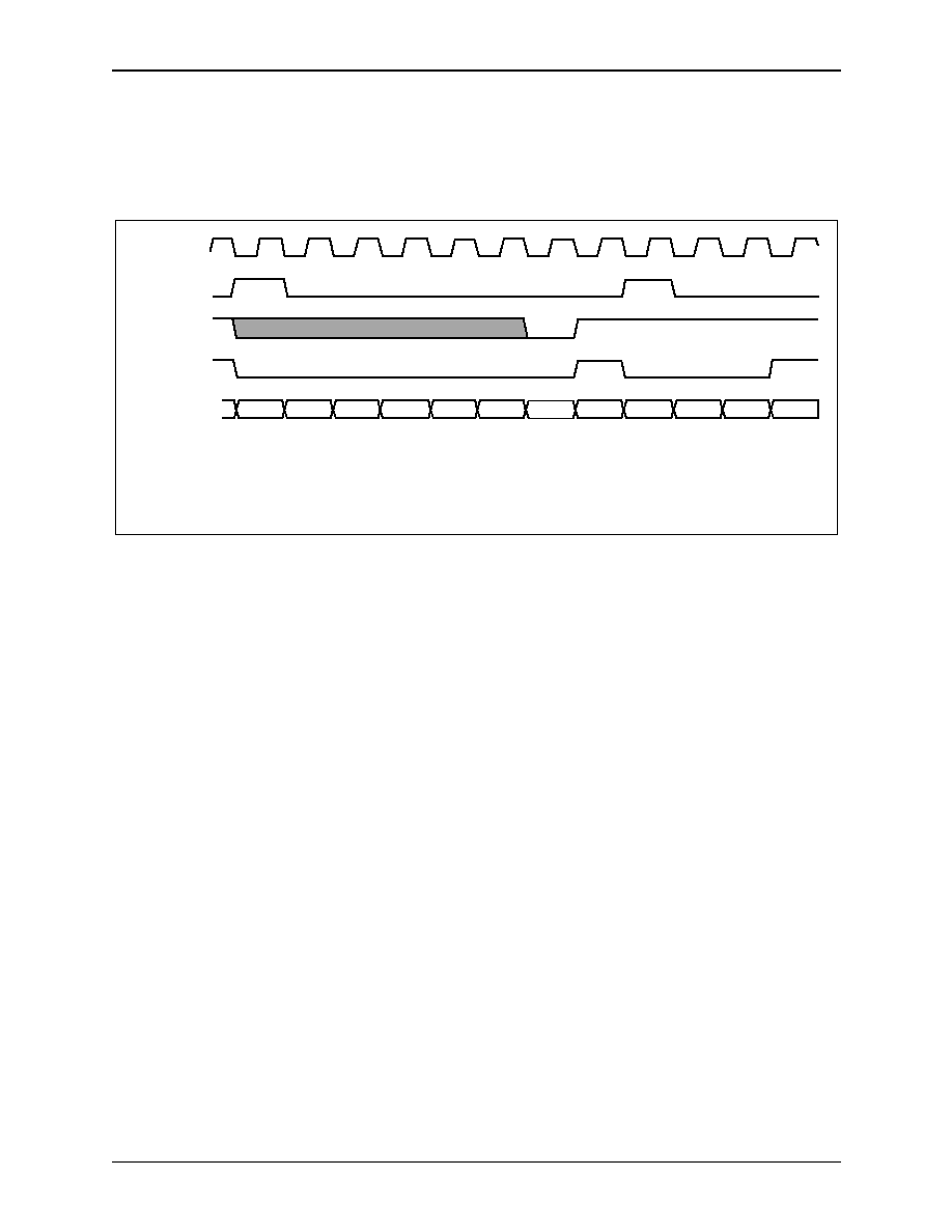
RS8234
12.0 ATM Utopia Interface
ATM ServiceSAR Plus with xBR Traffic Management
12.4 UTOPIA Mode Cell Handshake Timing
28234-DSH-001-B
Mindspeed Technologies
TM
12-5
In UTOPIA mode, the FRCTRL input can be connected to the RS8234
CLKD3 output; a 50% duty cycle clock derived by dividing CLK2X by three.
Figure 12-2. Transmit Timing in UTOPIA Mode with Cell Handshake
H1
***
P44
P45
P46
P47
P48
X
H1
***
P48
X
FRCTRL
TXSOC
TXEN*
TXD/TXPAR
(2)
(1)
(3)
(4)
100074_081
NOTE(S):
(1)
Once transfer of a cell is started, TxClav is sampled only on the last octet of a cell.
(2)
TxEN* goes active if TxClav is inactive at previous rising clock edge and a complete cell in the transmit FIFO buffer.
(3)
TxEN* goes inactive due to TxClav being active on previous cycle.
(4)
TxEN* goes inactive since a complete cell is not in the transmit FIFO buffer.
TXCLAV
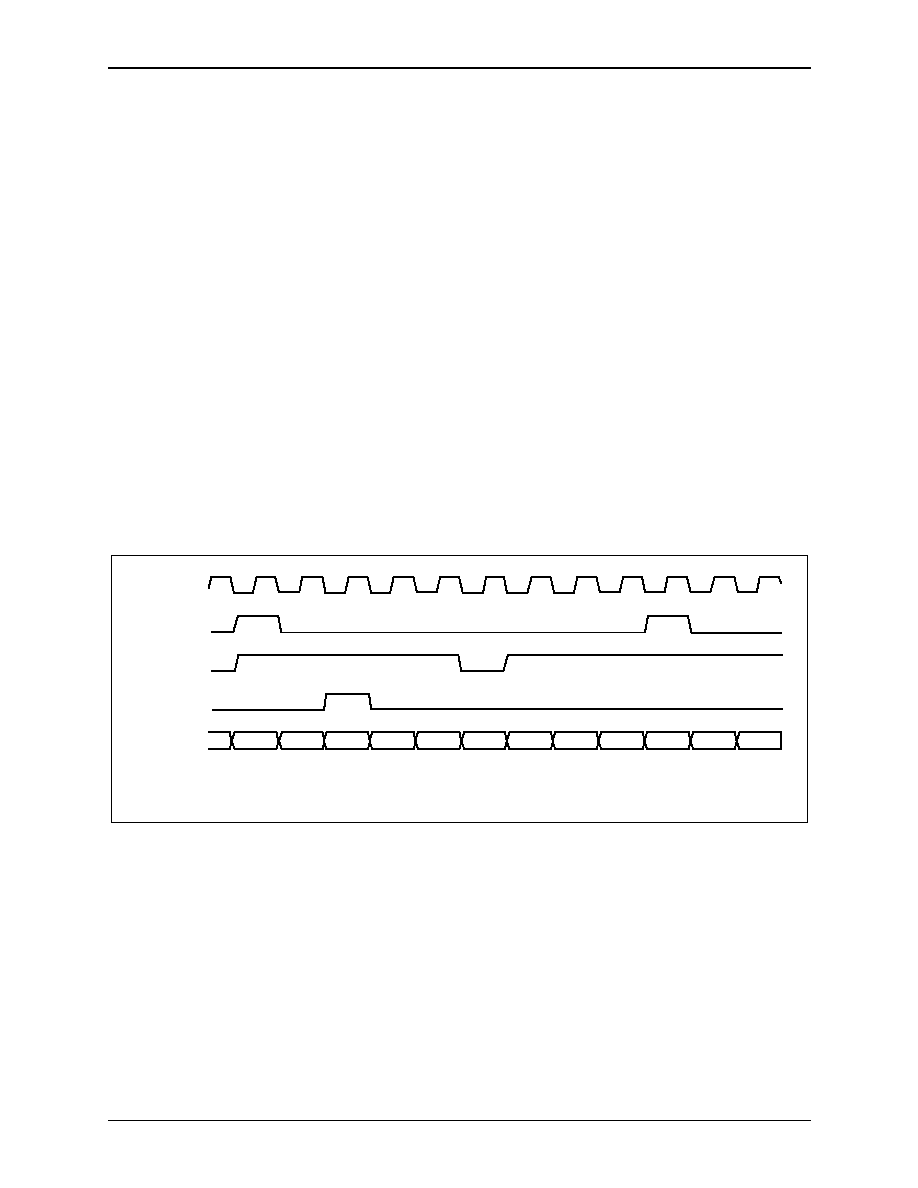
12.0 ATM Utopia Interface
RS8234
12.5 UTOPIA Mode Octet Handshake Timing
ATM ServiceSAR Plus with xBR Traffic Management
12-6
Mindspeed Technologies
TM
28234-DSH-001-B
12.5 UTOPIA Mode Octet Handshake Timing
If low, the UTOPIA_MODE bit in the CONFIG0 Register selects octet-level
handshaking. Received data is latched from the RXD[7:0] and RXPAR lines on
the rising edge of FRCTRL after RXEN* is sampled active (see
Figure 12-3
). The
8-bit odd parity computed over the RXD[7:0] lines is compared to the RXPAR
input. If in error, FR_PAR_ERR in the HOST_ISTAT0/LP_ISTAT0 registers is
set. No data is discarded upon a parity error unless the RSM_PHALT bit in the
RSM_CTRL Register is set to a logic high. If so, the reassembly coprocessor halts
upon a parity error.
The RXSOC signals the start of cell to the RS8234. The RXCLAV input is the
physical layer FIFO empty signal. When it is active, no data is present in the
physical receive FIFO. The physical layer device sets RXCLAV inactive when it
has an octet to transfer. The RS8234 sets RXEN* to a logic low if it can accept an
octet in the next clock cycle. The FR_RMODE bit in the CONFIG0 Register
should be set to a logic low in this mode.
Transmit data is driven on TXD[7:0] on the rising edge of FRCTRL when
TXEN* is asserted. TXEN* is only asserted when there is data in the RS8234
transmit FIFO. Simultaneously, the 8-bit odd parity computed over the TXD[7:0]
lines is driven on to the TXPAR output. The TXSOC line is driven by the framer
device to indicate start of cell. If the TXCLAV input is asserted by the framer
device, the framer device is full and can accept only one to four more octets. (See
Figure 12-2
.)
Figure 12-3. Receive Timing in UTOPIA Mode with Octet Handshake
H1
H2
H3
X
H4
X
H5
***
P48
H1
H2
H3
FRCTRL
RXSOC
RXCLAV
RXEN*
RXD/RXPAR
(1)
100074_082
NOTE(S):
(1)
RxEN* goes inactive only if there is no room for another octet in the receive FIFO buffer.
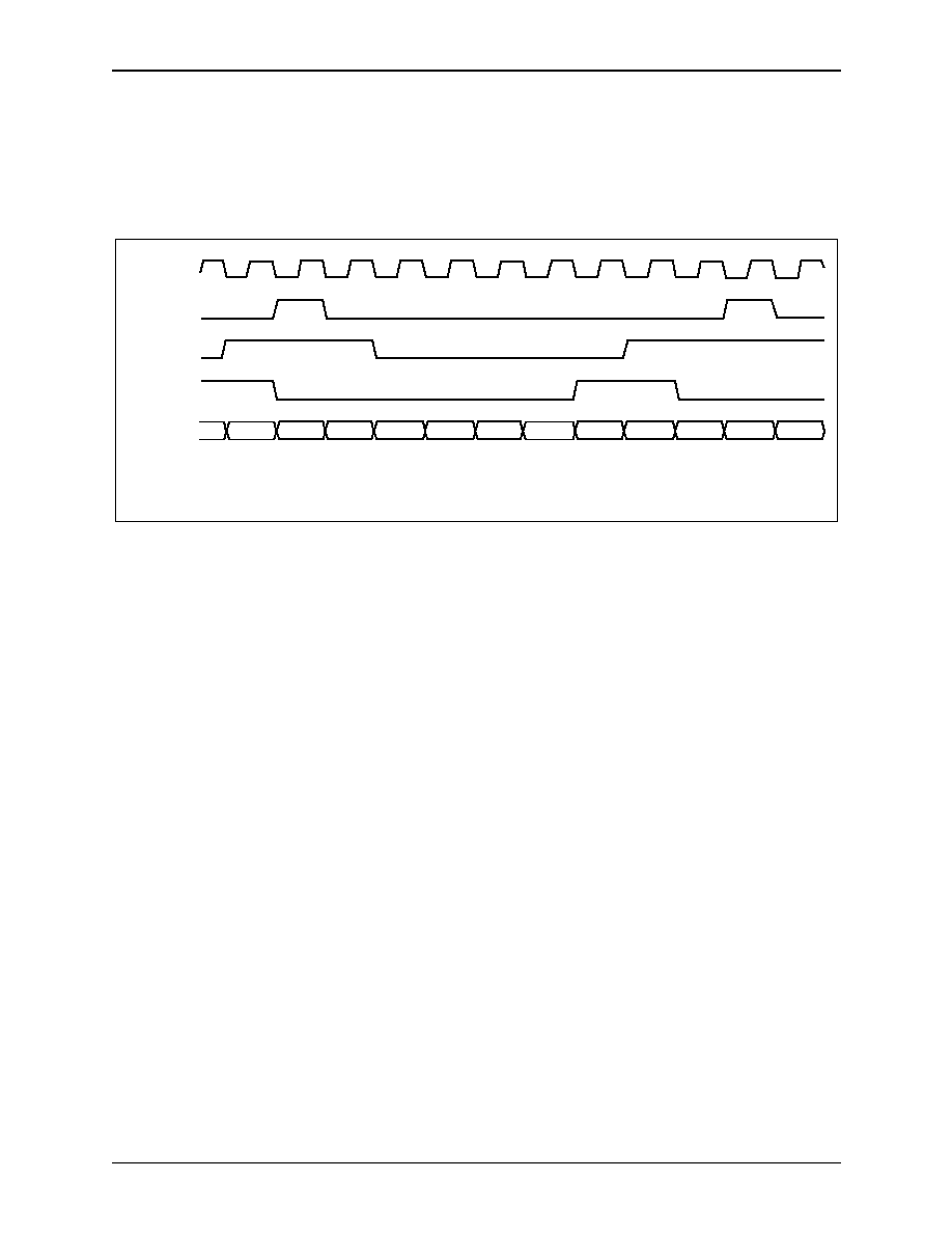
RS8234
12.0 ATM Utopia Interface
ATM ServiceSAR Plus with xBR Traffic Management
12.5 UTOPIA Mode Octet Handshake Timing
28234-DSH-001-B
Mindspeed Technologies
TM
12-7
In UTOPIA mode, the FRCTRL input may be connected to the RS8234
CLKD3 output, which is a 50% duty cycle clock derived by dividing the CLK2X
input by three.
Figure 12-4. Transmit Timing in UTOPIA Mode with Octet Handshake
H1
***
P45
P46
P47
X
P44
X
P48
X
H1
H2
FRCTRL
TXEN*
TXD/TXPAR
(1)
(2)
100074_083
NOTE(S):
(1)
TxEN* goes active of TxClav is inactive at previous rising clock edge and a complete cell in the transmit FIFO buffer.
(2)
TxEN* goes inactive one to four clock cycles after TxClav goes active.
TXSOC
TXCLAV
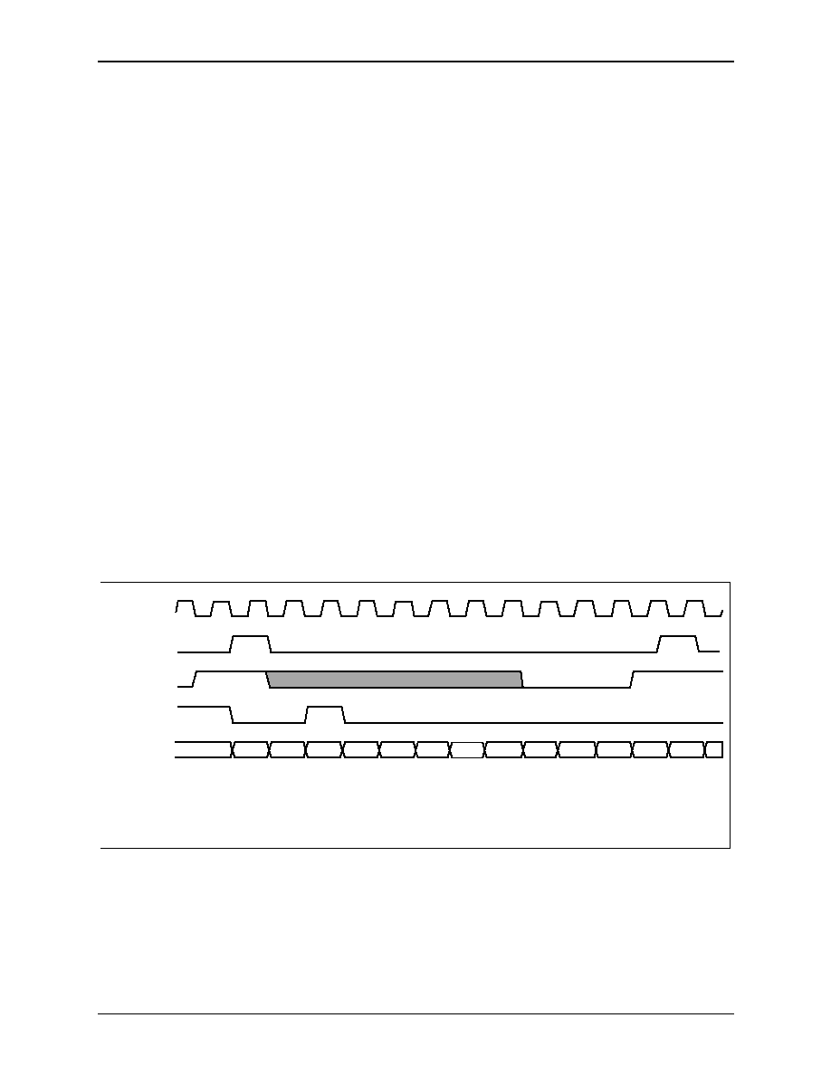
12.0 ATM Utopia Interface
RS8234
12.6 Slave UTOPIA Mode
ATM ServiceSAR Plus with xBR Traffic Management
12-8
Mindspeed Technologies
TM
28234-DSH-001-B
12.6 Slave UTOPIA Mode
The slave UTOPIA mode is similar to the UTOPIA mode, except the direction of
the enable signals and FIFO flags are reversed. This allows a switch fabric or
backplane to directly control the physical port. The transmit and receive enable
signals are generated by the physical layer instead of the RS8234. The TxFull*
signal is changed to the TxEmpty* signal and is an output of the RS8234. The
RxEmpty* signal is changed to the RxFull* signal, and is also an output of the
RS8234. This mode supports only a cell-level handshake protocol.
Received data is latched from the RXD[7:0] and RXPAR lines on the rising
edge of FRCTRL when RXEN* is active (see
Figure 12-5
). The 8-bit odd parity
computed over the RXD[7:0] lines is compared to the RXPAR input. If there is a
parity error, the FR_PAR_ERR bit is set in the HOST_ISTAT0/LP_ISTAT0
registers. No data is discarded upon a parity error unless the RSM_PHALT bit in
the RSM_CTRL Register is set to a logic high. If so, the reassembly coprocessor
halts upon a parity error. The RXSOC signals to the RS8234 the start of cell. The
RXCLAV output is the receive FIFO full signal. When it is active, the RS8234
cannot accept another cell. The RS8234 sets RXCLAV inactive when it has room
in the receive FIFO for another cell. The physical device sets RXEN* to a logic
low if it can transfer an octet. The FR_RMODE bit in the CONFIG0 Register
should be set to a logic low in this mode.
Figure 12-5. Receive Timing in Slave UTOPIA Mode
H2
H3
P44
***
P48
X
H1
H2
FRCTRL
RXEN*
RXD/TXPAR
(1)
(2)
(3)
P47
P46
P45
X
H1
X
100074_084
NOTE(S):
(1)
RxClav goes inactive when there is room in the receive FIFO buffer for a complete cell.
(2)
RxClav goes active when there is no longer room in the receive FIFO buffer for another complete cell.
(3)
RxEN* need not be inactive when RxClav is active.
RXSOC
RXCLAV
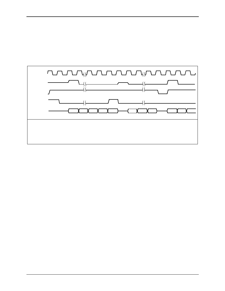
RS8234
12.0 ATM Utopia Interface
ATM ServiceSAR Plus with xBR Traffic Management
12.6 Slave UTOPIA Mode
28234-DSH-001-B
Mindspeed Technologies
TM
12-9
Transmit data is driven on TXD[7:0] on the rising edge of FRCTRL after
TXEN* is sampled asserted. Simultaneously, the 8-bit odd parity computed over
the TXD[7:0] lines is driven on to the TXPAR output. The TXSOC line is driven
by the SAR to indicate start of cell. If the TXCLAV output is asserted by the
RS8234, the transmit FIFO does not contain a complete cell. (See
Figure 12-2
.)
Figure 12-6. Transmit Timing in Slave UTOPIA Mode
H5
P1
P2
***
***
FRCTRL
TXSOC
TXCLAV
TXEN*
TXD/TXPAR
(1)
(4)
(3)
(3)
(2)
8234_006
NOTE(S):
(1)
TXCLAV goes active when a complete cell is in the transmit FIFO buffer.
(2)
Example of physical device deactivating TXEN*.
(3)
The TXD/TXPAR and TXSOC lines are three-stated (floated) when TXEN* is sampled high (de-asserted).
(4)
Physical device can keep TXEN* active while TXCLAV is inactive.
H1
P3
H2
H1
P48
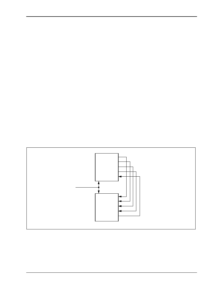
12.0 ATM Utopia Interface
RS8234
12.7 Loopback Mode
ATM ServiceSAR Plus with xBR Traffic Management
12-10
Mindspeed Technologies
TM
28234-DSH-001-B
12.7 Loopback Mode
The physical interface can be internally looped by setting the FR_LOOP bit in the
CONFIG0 Register to a logic high. This mode uses the internal system clock for
operation; therefore, a framer clock is not needed during loopback operation.
When the signal "fr_src_loop" equals one, the interface will loop back the
data and control signals, so the path from the segmentation coprocessor to the
reassembly coprocessor can be tested. The internal connections of the PHY
device interface signals are connected, as
Figure 12-7
illustrates. The transmit
side is put into the UTOPIA Mode and the receive side is put into the Reverse
UTOPIA Mode.
In this mode, the outputs of the chip, txd, txpar, txsoc, txen_, and rxclav_ are
three-stated, so there are no output conflicts with other devices connected to these
signals.
NOTE:
A reset of the reassembly coprocessor is required after the changing of the
FR_LOOP bit, because this changes the source of the clock to the physical
interface circuitry. To accomplish this reset, assert RSM_CTRL0
(RSM_RESET).
Figure 12-7. Source Loopback Mode Diagram
Transmit
Side in
UTOPIA
Mode
Receive
Side In
Reverse
UTOPIA
Mode
SYSCLK
TXD[15:0]
TXPAR
TXSOC
TXEN_
TXCLAV
RXD[15:0]
RXPAR
RXSOC
RXEN_
RXCLAV
100074_086

RS8234
12.0 ATM Utopia Interface
ATM ServiceSAR Plus with xBR Traffic Management
12.8 Receive Cell Synchronization Logic
28234-DSH-001-B
Mindspeed Technologies
TM
12-11
12.8 Receive Cell Synchronization Logic
The receive cell synchronization logic accepts a stream of octets (together with
error and cell boundary indications) from the receive ATM physical interface and
performs the following functions:
�
Maintains a sequence counter that marks the various components of an
ATM cell: the 5-byte ATM header, the 1-byte HEC field within the header,
and the 48-byte payload. The sequence counter is also used by the ATM
physical interface to check cell boundary synchronization.
�
Extracts and discards the HEC byte from each 53-byte ATM cell, leaving
52 bytes of cell data.
�
Formats consecutive 4-byte segments into 32-bit words; thus, the header
forms the first word, the first four bytes of the payload form the next word,
and so on. A total of thirteen 32-bit words are created from each 52-byte
cell after the HEC byte has been removed. The bytes within each word are
left-justified (big-endian format), i.e., the first byte received is the MSB of
the word.
�
Ensures that a complete cell (exactly 52 bytes) is always written to the
FIFO. If a synchronization error occurs, the FR_SYNC_ERR bit in the
HOST_ISTAT0/LP_ISTAT0 registers is set. The ATM physical interface
attempts to resynchronize with the data stream.
�
Sets the RSM_OVFL bit in the HOST_ISTAT0/LP_ISTAT0 registers if an
octet could not be transferred due to the receive FIFO being full.

12.0 ATM Utopia Interface
RS8234
12.9 Transmit Cell Synchronization Logic
ATM ServiceSAR Plus with xBR Traffic Management
12-12
Mindspeed Technologies
TM
28234-DSH-001-B
12.9 Transmit Cell Synchronization Logic
The transmit cell synchronization logic copies cell data from the transmit cell
FIFO to the transmit ATM physical interface while performing the following
functions:
�
Reads 32-bit words from the transmit cell FIFO and converts them to a
stream of octets, with the MSB of each 32-bit word corresponding to the
first byte derived from that word (big-endian format).
�
Maintains a sequence counter that delineates the various components of
each ATM cell (4-byte header, 48-byte payload) in the outgoing byte
stream.
�
Inserts a blank (all-zero) HEC byte, used as a placeholder, into the
outgoing byte stream representing each ATM cell. The HEC placeholder is
inserted after the first four bytes (the ATM header) have been transferred.
�
Generates appropriate cell delineation pulses to the transmit ATM physical
interface logic, for use in generating the TXSOC output, and also in
verifying synchronization with the framer device.
�
If the ATM physical transmit interface runs out of cells to transmit, the
device sets the SEG_UNFL bit in the HOST_ISTAT0/LP_ISTAT0
registers.
The transmit cell synchronization logic supplies a continuous stream of octets
to the transmit ATM physical interface unit, with cell delineation pulses at the
starting byte of every cell. Only complete 53-byte cells are supplied to the ATM
physical interface. If the transmit cell FIFO is empty, the transmit cell
synchronization logic indicates that no more data can be transferred to the framer.

28234-DSH-001-B
Mindspeed Technologies
TM
13-1
13.0 RS8234 Registers
13.1
Control and Status Registers
Control and status registers of the RS8234 are listed in
Table 13-1
. Detailed register descriptions are provided in
this section.
NOTE:
Note that byte enables are ignored by the RS8234 when writing to
control and status registers.
The access type terminology given below applies to all registers in this section. Each register description is
prefaced with the appropriate abbreviated access types.
Abbreviation
Description
R/W
Read and write access for both host and local processors
R/W H
Read and write access for host; read only access for local processor
R/W L
Read and write access for local; read only access for host processor
R/W R
Read and write access for both processors with restrictions
R/O-W/O B
Part of this register is read only; part write only by both processors
R/O
Read only access for both processors
13

13.0 RS8234 Registers
RS8234
13.1 Control and Status Registers
ATM ServiceSAR Plus with xBR Traffic Management
13-2
Mindspeed Technologies
TM
28234-DSH-001-B
Table 13-1. RS8234 Control and Status Registers (1 of 2)
Address
Name
Type
Description
0x00
CLOCK
R/W
Real Time Clock Register
0x04
ALARM1
R/W
Alarm Register 1
0x08
Reserved
�
Not Implemented
0x0C
SYS_STAT
R/O
System Status Register
0x10
Reserved
�
Not Implemented
0x14
CONFIG0
R/W
Basic Configuration And Control Register 0
0x18
Reserved
�
Not Implemented.
Must be set to 0.
0x1c
INT_DELAY
R/W
Interrupt Delay Register
0x20-0x7c
Reserved
-
Not Implemented
0x80
SEG_CTRL
R/W
Segmentation Control Register
0x84
SEG_VBASE
R/W
SEG VCC Table and Schedule Table Base Address Register
0x88
SEG_PMBASE
R/W
SEG PM Table and Bucket Table Base Address Register
0x8c
SEG_TXBASE
R/W
Segmentation Transmit Queue Base Register
0x90-0x9c
Reserved
-
Not Implemented
0xa0
SCH_PRI
R/WB
Schedule Priority Register
0xa4
SCH_PRI_2
R/W
Schedule Priority Control Register 2
0xa8
SCH_SIZE
R/W
Schedule Size and Slot Minimum Drain Rate Register
0xac
SCH_CTRL
R/W
Scheduler Control Register
0xb0
SCH_ABR_MAX
R/W
Maximum ABR VCC_INDEX Register
0xb4
SCH_ABR_CON
R/W
Schedule ABR Constant Register
0xb8
SCH_ABRBASE
R/W
ABR Decision Table Lookup Base Register
0xbc
SCH_CNG
R/W
ABR Congestion Notification Register
0xc0
PCR_QUE_INT01
R/W
PCR Queue Interval 0 and 1 Register
0xc4
PCR_QUE_INT23
R/W
PCR Queue Interval 2 and 3 Register
0xc8�0xeC
Reserved
�
Not Implemented
0xf0
RSM_CTRL0
R/W
Reassembly Control Register 0
0xf4
RSM_CTRL1
R/W
Reassembly Control Register 1
0xf8
RSM_FQBASE
R/W
Reassembly Free Buffer Queue Base Register
0xfC
RSM_FQCTRL
R/W
Reassembly Free Buffer Queue Control Register
0x100
RSM_TBASE
R/W
Reassembly Table Base Register
0x104
RSM_TO
R/W
Reassembly Time-out Register
0x108
RS_QBASE
R/W
Reassembly/Segmentation Queue Base Address Register
0x10C�0x15C
Reserved
�
Not Implemented
0x160
CELL_XMIT_CNT
R/O
ATM Cells Transmitted Counter

RS8234
13.0 RS8234 Registers
ATM ServiceSAR Plus with xBR Traffic Management
13.1 Control and Status Registers
28234-DSH-001-B
Mindspeed Technologies
TM
13-3
0x164
CELL_RCVD_CNT
R/O
ATM Cells Received Counter
0x168
CELL_DSC_CNT
R/O
ATM Cells Discarded Counter
0x16C
AAL5_DSC_CNT
R/O
AAL5 PDUs Discarded Counter
0x170 - 0x19C
Reserved
-
Not Implemented
0x1a0
HOST_MBOX
R/W L
Host Mailbox Register
0x1a4
HOST_ST_WR
R/O
Host Status Write Register
0x1a8-0x1ac
Reserved
-
Not Implemented
0x1b0
LP_MBOX
R/W H
Local Processor Mailbox Register
0x1b4-0x1bc
Reserved
-
Not Implemented
0x1c0
HOST_ISTAT0
R/O
Host Processor Interrupt Status Register 0
0x1c4
HOST_ISTAT1
R/O
Host Processor Interrupt Status Register 1
0x1c8-0x1cc
Reserved
-
Not Implemented
0x1d0
HOST_IMASK0
R/W H
Host Interrupt Mask Register 0
0x1d4
HOST_IMASK1
R/W H
Host Interrupt Mask Register 1
0x1d8-0x1dc
Reserved
�
Not Implemented
0x1e0
LP_ISTAT0
R/O
Local Processor Interrupt Status Register 0
0x1e4
LP_ISTAT1
R/O
Local Processor Interrupt Status Register 1
0x1e8-0x1ec
Reserved
�
Not Implemented
0x1f0
LP_IMASK0
R/W L
Local Processor Interrupt Mask Register 0
0x1f4
LP_IMASK1
R/W L
Local Processor Interrupt Mask Register 1
0x1f8-0x1fc
Reserved
�
Not Implemented
Table 13-1. RS8234 Control and Status Registers (2 of 2)
Address
Name
Type
Description

13.0 RS8234 Registers
RS8234
13.2 System Registers
ATM ServiceSAR Plus with xBR Traffic Management
13-4
Mindspeed Technologies
TM
28234-DSH-001-B
13.2 System Registers
0x00 - Real-Time Clock Register (CLOCK)
This register contains the 32-bit real time clock. It is incremented by the system clock (SYSCLK), which has
been divided by the DIVIDER[6:0] field in the CONFIG0 register. It can be written to any value by each
processor, and can generate an interrupt on the RTC_OVFL status bit in the LP_ISTAT0 register when it
overflows from 0xFFFFFFFF to 0x0.
0x04 - Alarm Register 1 (ALARM1)
This register contains a 32-bit value which is compared against the CLOCK register. When the two registers are
equal, the ALARM1 status bit in the LP_ISTAT0 register is latched and can be enabled to cause an interrupt to
the local processor. To implement a periodic interrupt, add a constant value to this register after each interrupt.
Bit
Field
Size
Name
Description
31�0
32
CLOCK[31:0]
Real-time clock value.
Bit
Field
Size
Name
Description
31�0
32
ALARM1[31:0]
ALARM1 comparison value.
RS8234
13.0 RS8234 Registers
ATM ServiceSAR Plus with xBR Traffic Management
13.2 System Registers
28234-DSH-001-B
Mindspeed Technologies
TM
13-5
0x0c - System Status Register (SYS_STAT)
The System Status Register provides read-only system status. This register reflects the device ID and version
information for the part, as well as pin programmable options that otherwise might not be visible to the
processors. It also contains expanded information for the status located in the HOST_ISTAT0 and LP_ISTAT0
registers.
0x14 - Configuration Register 0 (CONFIG0)
This register provides all of the control and configuration bits that are not associated with the reassembly and
segmentation coprocessors. The majority of these bits are configuration (which occurs at initialization time) and
are not changed dynamically. The assertion of the HRST* system reset pin will clear all of the bits in the
CONFIG0 register except for MEMCTRL, which will be set high.
Bit
Field
Size
Name
Description
31�17
15
Reserved
Not implemented at this time.
16�12
5
PCI_BUS_STATUS
[4:0]
The status bits are as follows:
4 = Target Abort
3 = Master Abort
2 = Parity Error
1 = Interface Disabled
0 = Internal Failure
Reflects corresponding error bits in the PCI Configuration register. Bits are
reset by either a write to the PCI Configuration register by the host, or by
setting CONFIG0 (PCI_ERR_RESET) bit.
11
1
RAMMODE
Reflects the state of the RAMMODE input pin.
10
1
PROCMODE
Reflects the state of the PROCMODE input pin.
9, 8
2
FRCFG[1:0]
Reflects the state of the FRCFG[1:0] input pins.
7�4
4
VERSION [3:0]
Version number for the RS8234; for Rev A set to zero, for Rev B set to one,
for Rev C set to two, for Rev D set to three, for Rev E set to four, and for Rev
F set to five.
3�0
4
DEVICE[3:0]
Device ID for the RS8234; set to two.
Bit
Field
Size
Name
Description
31
1
LP_ENABLE
When set, this bit causes the PRST* output pin to be high. This can be
used to reset the local processor.
30
1
GLOBAL_RESET
When set, this bit causes reset of the segmentation and reassembly
coprocessors as well as all latched status.
29
1
PCI_MSTR_RESET
When set, this bit resets the PCI master logic. Once active, this bit must
stay active for 16 cycles of the HCLK input signal.
28
1
PCI_ERR_RESET
When set, resets all PCI error bits in the PCI configuration, including RMA,
RTA, DPR, INTF_DIS, INT_FAIL, and MERROR. This also re-enables PCI
master operation.
27�26
2
Reserved
Always set to zero.

13.0 RS8234 Registers
RS8234
13.2 System Registers
ATM ServiceSAR Plus with xBR Traffic Management
13-6
Mindspeed Technologies
TM
28234-DSH-001-B
25
1
PHY2_EN
Enables the second PHY device memory space in standalone operation.
24
1
INT_LBANK
When set, allows only byte 0 and 1 writes to address space
0x1000�0x10ff and 0x1400�0x14ff. This allows endian neutral access of
the Status Queue Base Table READ_UD field by the host or local
processor.
23
1
Reserved
Always set to zero.
22
1
PCI_READ_MULTI
When this bit is set, the SAR's PCI Master implements the PCI Read
Multiple Command. Otherwise, the PCI Master implements the PCI Read
Command.
21
1
PCI_ARB
Selects PCI Master arbitration scheme. When a logic high, enables
round-robin between read and write requests. When a logic low, reads
have priority over writes.
20�16
5
STATMODE[4:0]
Selects which internal status to output on the STAT[1:0] output pins.
15
1
FR_RMODE
(BT8222/3)
Controls reassembly start of cell processing. When set low, processing
starts after the first two words of a cell are received. When set high, a
complete cell must be in reassembly FIFO before cell is processed.
14
1
FR_LOOP
When set, this bit enables loopback of cells at the ATM physical interface.
Loopback uses SYSCLK.
13
1
UTOPIA_MODE
Selects byte or cell UTOPIA handshake mode.
0 = Octet handshake
1 = Cell handshake
12
1
ENDIAN
Selects between Little and Big Endian host data structures.
0 = Little Endian
1 = Big Endian
11
1
LP_BWAIT
Selects zero or one wait states between consecutive data cycles during
local processor burst accesses. Set to logic low for standalone operation
mode.
10
1
MEMCTRL
Selects zero or one wait states SAR shared memory (1 or 2 cycle).
9�7
3
BANKSIZE[2:0]
Selects size of memory banks for contiguous memory support. See
Section 9.2
, for further explanation.
6�0
7
DIVIDER[6:0]
Prescaler for SYSCLK which advances the counter in the CLOCK Register.
SYSCLK is divided by the divider value; if zero, divided by 128.
Bit
Field
Size
Name
Description

RS8234
13.0 RS8234 Registers
ATM ServiceSAR Plus with xBR Traffic Management
13.2 System Registers
28234-DSH-001-B
Mindspeed Technologies
TM
13-7
0x1c - Interrupt Delay Register (INT_DELAY)
Bit
Field
Size
Name
Description
31�11
21
Reserved
Set to zero.
10
1
TIMER_LOC
If logic high, interrupt hold off timer used with local interrupt; else with host
interrupt.
9
1
EN_TIMER
Enable status queue interrupt timer delay.
8
1
EN_STAT_CNT
Enable status queue interrupt counter delay.
7-0
8
STAT_CNT[7:0]
Number of status queue entries written before allowing interrupt to
propagate to output pin.

13.0 RS8234 Registers
RS8234
13.3 Segmentation Registers
ATM ServiceSAR Plus with xBR Traffic Management
13-8
Mindspeed Technologies
TM
28234-DSH-001-B
13.3 Segmentation Registers
0x80 - Segmentation Control Register (SEG_CTRL)
This register contains general control bits for the segmentation coprocessor. The assertion of the HRST* system
reset pin or GLOBAL_RESET bit in the CONFIG0 register will cause the clearing of the SEG_ENABLE
control bit.
Bit
Field
Size
Name
Description
31
1
SEG_ENABLE
Segmentation Enable--enables segmentation coprocessor. If disabled, the
segmentation coprocessor will halt on a cell boundary.
30
1
SEG_RESET
Segmentation Reset --resets segmentation coprocessor and pointers.
29-27
3
VBR_OFFSET
Offset from schedule slot priority to general priority. (VBR_OFFSET + (#
VBR/ABR priorities)
<
7.) Not active if USE_SCH_CTRL is asserted.
26
1
SEG_GFC
Enable segmentation GFC processing. The segmentation machine is
disabled when the SAR receives cells with GFC halt set. GFC priority
queues (set in the SCH_PRI register) are active for one cell for each
received cell with GFC SET_A bit = 1.
25
1
DBL_SLOT
Each schedule slot occupies two words. Not active if USE_SCH_CTRL is
asserted.
24
1
CBR_TUN
Use first entry in each schedule slot for CBR/tunnel traffic.
23
1
ADV_ABR_TMPLT
Advanced ABR template mode. When logic high, per-connection MCR and
ICR enabled. When logic low, per-template MCR and ICR enabled.
22
1
USE_SCH_CTRL
Activate the use of SLOT_DEPTH, the 4-bit VBR_OFFSET field, and
TUN_PRI0_OFFSET from the SCH_CTRL register. De-activate the use of
DBL_SLOT and the 3-bit VBR_OFFSET field from the SEG_CTRL register.
21-16
6
Reserved
Program and read as zero.
15-12
4
TX_FIFO_LEN
Depth of transmit FIFO in cells. Valid range is 3�9. To ensure optimum
performance, the depth of the FIFO should be at least three.
11
1
CLP0_EOM
Set CLP in ATM header to zero on last cell of CPCS-PDU.
10-6
5
OAM_STAT_ID
Status queue ID for buffer descriptors with OAM_STAT set.
5
1
SEG_ST_HALT
Enables a status queue entry for a VCC halted with a partially segmented
packet.
4
1
SEG_LS_DIS
Segmentation Local Status Disable--Disable segmentation check for SAR
shared memory status queue full condition. If this bit is not set, the
segmentation coprocessor will not segment any cells for a VCC assigned
to a full SAR shared memory status queue. This bit can be used to disable
overflow checking when the queues are sized large enough to prevent
overflow.

RS8234
13.0 RS8234 Registers
ATM ServiceSAR Plus with xBR Traffic Management
13.3 Segmentation Registers
28234-DSH-001-B
Mindspeed Technologies
TM
13-9
0x84 - Segmentation VCC Table and Schedule Table Base Address Register
(SEG_VBASE)
The SEG_VBASE register sets the base address in SAR shared memory for the segmentation VCC table and the
schedule table. Both base addresses are 128-byte aligned and only the 16 most significant bits of the address are
specified in the SEG_VBASE register.
0x88 - Segmentation PM Base Register (SEG_PMBASE)
The SEG_PMBASE register sets the base address in SAR shared memory for the VBR bucket table and the
performance monitoring table. Both base addresses are 128-byte aligned and only the 16 most significant bits of
the address are specified in the SEG_PMBASE register.
3
1
SEG_HS_DIS
Segmentation Host Status Disable--Disable segmentation check for PCI
memory status queue full condition. If this bit is not set, the segmentation
coprocessor will not segment any cells for a VCC assigned to a full PCI
memory status queue. This bit can be used to disable overflow checking
when the queues are sized large enough to prevent overflow.
2
1
TX_RND
Set for transmit queue servicing in round-robin order.
Clear for transmit queue servicing in priority order (31 is highest priority).
1-0
2
TR_SIZE[1:0]
Number of entries in each transmit queue.
00 = 64
01 = 256
10 = 1,024
11 = 4,096
Bit
Field
Size
Name
Description
Bit
Field
Size
Name
Description
31-16
16
SEG_SCHB[15:0]
Base address for the schedule table.
15-0
16
SEG_VCCB[15:0]
Base address for the segmentation VCC table.
Bit
Field
Size
Name
Description
31-16
16
SEG_BCKB[15:0]
Base address for the VBR bucket table. (See
Section 6.2.4
, for details on
loading bucket table entries.)
15-0
16
SEG_PMB[15:0]
Base address for the performance monitoring table.

13.0 RS8234 Registers
RS8234
13.3 Segmentation Registers
ATM ServiceSAR Plus with xBR Traffic Management
13-10
Mindspeed Technologies
TM
28234-DSH-001-B
0x8c - Segmentation Transmit Queue Base Register (SEG_TXBASE)
The SEG_TXBASE register sets the base address in SAR shared memory for the transmit queues and enables
the individual queues. The base address is 128-byte aligned and only the 16 most significant bits of the address
are specified in the SEG_TXBASE register.
Bit
Field
Size
Name
Description
31-16
16
SEG_TXB[15:0]
Base address for the transmit queues.
15-13
3
Reserved
Program and read as zero.
12-5
8
XMIT_INTERVAL[7:0]
Interval for transmit queue READ_UD_PNTR update.
4-0
5
TX_EN
Transmit queues 0-TX_EN are enabled.

RS8234
13.0 RS8234 Registers
ATM ServiceSAR Plus with xBR Traffic Management
13.4 Scheduler Registers
28234-DSH-001-B
Mindspeed Technologies
TM
13-11
13.4 Scheduler Registers
0xa0 - Schedule Priority Register (SCH_PRI)
This register specifies the use of each global priority pointer, for priority queues 0 through 7.
Bit
Field
Size
Name
Description
31
1
QPCR_ENA7
Enable PCR limits on global priority pointer 7.
30
1
QPCR_ENA6
Enable PCR limits on global priority pointer 6.
29
1
QPCR_ENA5
Enable PCR limits on global priority pointer 5.
28
1
QPCR_ENA4
Enable PCR limits on global priority pointer 4.
27
1
QPCR_ENA3
Enable PCR limits on global priority pointer 3.
26
1
QPCR_ENA2
Enable PCR limits on global priority pointer 2.
25
1
QPCR_ENA1
Enable PCR limits on global priority pointer 1.
24
1
QPCR_ENA0
Enable PCR limits on global priority pointer 0.
23
1
Reserved
Program and read as zero.
22
1
TUN_ENA7
Enable tunnel on global priority pointer 7.
21
1
GFC7
Enable GFC on priority pointer 7.
20
1
Reserved
Program and read as zero.
19
1
TUN_ENA6
Enable tunnel on global priority pointer 6.
18
1
GFC6
Enable GFC on priority pointer 6.
17
1
Reserved
Program and read as zero.
16
1
TUN_ENA5
Enable tunnel on global priority pointer 5.
15
1
GFC5
Enable GFC on priority pointer 5.
14
1
Reserved
Program and read as zero.
13
1
TUN_ENA4
Enable tunnel on global priority pointer 4.
12
1
GFC4
Enable GFC on priority pointer 4.
11
1
Reserved
Program and read as zero.
10
1
TUN_ENA3
Enable tunnel on global priority pointer 3.
9
1
GFC3
Enable GFC on priority pointer 3.
8
1
Reserved
Program and read as zero.
7
1
TUN_ENA2
Enable tunnel on global priority pointer 2.
6
1
GFC2
Enable GFC on priority pointer 2.
5
1
Reserved
Program and read as zero.

13.0 RS8234 Registers
RS8234
13.4 Scheduler Registers
ATM ServiceSAR Plus with xBR Traffic Management
13-12
Mindspeed Technologies
TM
28234-DSH-001-B
0xa4 - Schedule Priority Control Register 2 (SCH_PRI_2)
The SCH_PRI_2 register sets the enables for GFC, CBR tunneling and PCR limits, on global priority queues 8
through 15.
4
1
TUN_ENA1
Enable tunnel on global priority pointer 1.
3
1
GFC1
Enable GFC on priority pointer 1.
2
1
Reserved
Program and read as zero.
1
1
TUN_ENA0
Enable tunnel on global priority pointer 0.
0
1
GFC0
Enable GFC on priority pointer 0.
Bit
Field
Size
Name
Description
Bit
Field
Size
Name
Description
31
1
QPCR_ENA_15
Enable PCR limits on global priority pointer 15.
30
1
QPCR_ENA_14
Enable PCR limits on global priority pointer 14.
29
1
QPCR_ENA_13
Enable PCR limits on global priority pointer 13.
28
1
QPCR_ENA_12
Enable PCR limits on global priority pointer 12.
27
1
QPCR_ENA_11
Enable PCR limits on global priority pointer 11.
26
1
QPCR_ENA_10
Enable PCR limits on global priority pointer 10.
25
1
QPCR_ENA_9
Enable PCR limits on global priority pointer 9.
24
1
QPCR_ENA_8
Enable PCR limits on global priority pointer 8.
23
1
Reserved
Program and read as zero.
22
1
TUN_ENA_15
Enable tunnel on global priority pointer 15.
21
1
GFC15
Enable GFC on global priority pointer 15.
20
1
Reserved
Program and read as zero.
19
1
TUN_ENA_14
Enable tunnel on global priority pointer 14.
18
1
GFC14
Enable GFC on global priority pointer 14.
17
1
Reserved
Program and read as zero.
16
1
TUN_ENA_13
Enable tunnel on global priority pointer 13.
15
1
GFC13
Enable GFC on global priority pointer 13.
14
1
Reserved
Program and read as zero.
13
1
TUN_ENA_12
Enable tunnel on global priority pointer 12.
12
1
GFC12
Enable GFC on global priority pointer 12.
11
1
Reserved
Program and read as zero.
10
1
TUN_ENA_11
Enable tunnel on global priority pointer 11.
9
1
GFC11
Enable GFC on global priority pointer 11.

RS8234
13.0 RS8234 Registers
ATM ServiceSAR Plus with xBR Traffic Management
13.4 Scheduler Registers
28234-DSH-001-B
Mindspeed Technologies
TM
13-13
0xa8 - Schedule Size Register (SCH_SIZE)
The SCH_SIZE register sets the size of the schedule table in schedule slots and the period of a schedule slot in
system clocks.
0xac - Scheduler Control Register (SCH_CTRL)
The SCH_CTRL register defines the configured schedule slot and priority and VBR offsets, when 16 priority
queues are used.
8
1
Reserved
Program and read as zero.
7
1
TUN_ENA_10
Enable tunnel on global priority pointer 10.
6
1
GFC10
Enable GFC on global priority pointer 10.
5
1
Reserved
Program and read as zero.
4
1
TUN_ENA_9
Enable tunnel on global priority pointer 9.
3
1
GFC9
Enable GFC on global priority pointer 9.
2
1
Reserved
Program and read as zero.
1
1
TUN_ENA_8
Enable tunnel on global priority pointer 8.
0
1
GFC8
Enable GFC on global priority pointer 8.
Bit
Field
Size
Name
Description
Bit
Field
Size
Name
Description
31-16
16
TBL_SIZE[15:0]
Size of schedule table in schedule slots.
15-14
2
Reserved
Program and read as zero.
13-0
14
SLOT_PER[13:0]
Number of system clocks per schedule slot. The value written to the
register should be (SLOT_PER - 1). Minimum bound for SLOT_PER
value = 70.
Bit
Field
Size
Name
Description
31-27
5
Reserved
Program and read as zero.
26
1
Reserved
NOTE:
Must be set to
0
during initialization unless using an external
scheduler clock.
25-15
11
Reserved
Program and read as zero.
14-12
3
SLOT_DEPTH
Depth of the schedule slot is set to 1 + SLOT_DEPTH words. Active only if
USE_SCH_CTRL is asserted.
11-10
2
Reserved
Program and read as zero.
9-6
4
TUN_PRI0_OFFSET
Offset from the TUN_PRI_0 field in the schedule table and CBR VCC table.
Active only if USE_SCH_CTRL is asserted.

13.0 RS8234 Registers
RS8234
13.4 Scheduler Registers
ATM ServiceSAR Plus with xBR Traffic Management
13-14
Mindspeed Technologies
TM
28234-DSH-001-B
0xb0 - Maximum ABR VCC_INDEX Register (SCH_ABR_MAX)
The SCH_ABR_MAX register defines the configured maximum ABR VCC index.
0xb4 - Schedule ABR Constant Register (SCH_ABR_CON)
The SCH_ABR_CON register sets the ABR TRM and ADTF timeout. Timeout values are in units of 64 cell
slots.
access types: R/W
5-4
2
Reserved
Program and read as zero.
3-0
4
VBR_OFFSET
Offset from schedule slot priority to general priority. Active only if
USE_SCH_CTRL is asserted.
Bit
Field
Size
Name
Description
31-16
16
Reserved
Program and read as zero.
15-0
16
VCC_MAX
Maximum ABR VCC index.
Bit
Field
Size
Name
Description
Bit
Field
Size
Name
Description
31-16
16
ABR_TRM
ABR TRM parameter.
Parameter value is SYSCLK period x SLOT_PER x ABR_TRM x 64.
15-0
16
ABR_ADTF
ABR ADTF parameter.
Parameter values is SYSCLK period x SOT_PER x ABR_ADTF x 64.

RS8234
13.0 RS8234 Registers
ATM ServiceSAR Plus with xBR Traffic Management
13.4 Scheduler Registers
28234-DSH-001-B
Mindspeed Technologies
TM
13-15
0xb8 - ABR Decision Table Lookup Base Register (SCH_ABRBASE)
The SCH_ABRBASE register sets the base address in SAR shared memory for the ABR decision table. This
address is 128-byte aligned, and only the 16 most significant bits of the address are specified in the
SCH_ABRBASE register.
0xbc - ABR Congestion Register (SCH_CNG)
The SCH_CNG register sets each reassembly free buffer queue to a congested or non-congested state for
transmitted reverse RM cells.
Bit
Field
Size
Name
Description
31-29
3
Reserved
Program and read as zero.
28
1
OOR_EN
Enable ABR out-of-rate Forward RM cell generation.
27-16
12
OOR_INT
ABR out-of-rate Forward RM cell interval. A VCC is examined for an
out-of-rate cell every OOR_INT schedule slots.
15-0
16
SCH_ABRB[15:0]
Base address for the ABR decision table.
Bit
Field
Size
Name
Description
31-0
32
FBQ_CNG[31:0]
Congestion state for each free buffer queue.

13.0 RS8234 Registers
RS8234
13.4 Scheduler Registers
ATM ServiceSAR Plus with xBR Traffic Management
13-16
Mindspeed Technologies
TM
28234-DSH-001-B
0xc0 - PCR Queue Interval 0 and 1 Register (PCR_QUE_INT01)
The PCR_QUE_INT01 register fields are used to store the two lower PCR values used in PCR shaping on
priority queues that have been enabled for PCR shaping by setting the QPCR_ENAx bits in the SCH_PRI
register. QPCR_INTx values are used in order: 3, 2, 1, and 0; highest to lowest. PCR is determined by:
1/(QPCR_INTx x SYSCLK_period x SLOT_PER).
0xc4 - PCR Queue Interval 2 and 3 Register (PCR_QUE_INT23)
The PCR_QUE_INT23 register fields are used to store the two highest PCR values used in PCR shaping on
priority queues that have been enabled for PCR shaping by setting the QPCR_ENAx bits in the SCH_PRI
register. QPCR_INTx values are used in order: 3, 2, 1, and 0; highest to lowest. PCR is determined by:
1/(QPCR_INTx x SYSCLK_period x SLOT_PER).
Bit
Field
Size
Name
Description
31-16
16
QPCR_INT1
The assigned PCR interval, entered as number of schedule table slots,
used to map to the 3rd-highest priority queue that is enabled for PCR
shaping (using the QPCR_ENAx bits in the SCH_PRI register).
15-0
16
QPCR_INT0
The assigned PCR interval, entered as number of schedule table slots,
used to map to the 4th-highest priority queue that is enabled for PCR
shaping (using the QPCR_ENAx bits in the SCH_PRI register).
Bit
Field
Size
Name
Description
31-16
16
QPCR_INT3
The assigned PCR interval, entered as number of schedule table slots,
used to map to the highest priority queue that is enabled for PCR shaping
(using the QPCR_ENAx bits in the SCH_PRI register).
15-0
16
QPCR_INT2
The assigned PCR interval, entered as number of schedule table slots,
used to map to the 2nd-highest priority queue that is enabled for PCR
shaping (using the QPCR_ENAx bits in the SCH_PRI register).

RS8234
13.0 RS8234 Registers
ATM ServiceSAR Plus with xBR Traffic Management
13.5 Reassembly Registers
28234-DSH-001-B
Mindspeed Technologies
TM
13-17
13.5 Reassembly Registers
0xf0 - Reassembly Control Register 0 (RSM_CTRL0)
The Reassembly Control Register 0 contains the general control bits for the reassembly coprocessor. The
assertion of the HRST* system reset pin or the GLOBAL_RESET bit in the CONFIG0 register will clear the
RSM_ENABLE control bit.
Bit
Field
Size
Name
Description
31
1
RSM_ENABLE
Reassembly enable. Initiates an incoming transfer if set, and halts it if reset.
If this bit is reset while the reassembly coprocessor is running, it
temporarily suspends the activities of the reassembly coprocessor logic.
Suspension takes place on a cell boundary, i.e., between the completion of
all processing and transfers required for the current cell, and the start of
processing for the next cell. The hold can be removed and the transfer
resumed by setting the RSM_ENABLE bit. This bit will also be set low
internally on certain reassembly error conditions. This includes parity error
with PHALT_EN. In this case, the error condition should be corrected and
the RSM_ENABLE bit set high to resume operation.
30
1
RSM_RESET
Reassembly reset. Forces a hardware reset of the reassembly coprocessor
when asserted. It must be deasserted before the reassembly coprocessor
will resume normal operation.
29
1
Reserved
Program and read as zero.
28
1
VPI_MASK
VPI Mask enable. Used to select UNI/NNI header operation in the direct
index method. When a logic high, the four MSBs of the header are masked
for UNI operation. This also controls the Index Table size. A UNI table is 256
entries and a NNI table is 4,096.
27-24
4
Reserved
Program and read as zero.
23-18
6
Reserved
Program and read as zero.
17
1
RSM_PHALT
Reassembly coprocessor halt on parity error detect. The reassembly
coprocessor will halt the incoming channel logic if a parity error is detected
and the RSM_PHALT bit is set.
16
1
Reserved
Program and read as zero.
15
1
FWALL_EN
Firewall enable. Enables free buffer queue firewalling of user cells. If set,
this bit enables the per connection free buffer queue firewall. Each
connection that firewall is active in must have the FW_EN bit set to a logic
high in the VCC table.
14
1
RSM_FBQ_DIS
Free Buffer Queue Underflow Protection Disable. When a logic high, the
reassembly coprocessor ignores the VLD bit in the free buffer queue when a
new buffer is required. The periodic writing of the read index pointer to
host/SAR shared memory is also disabled.
13
1
RSM_STAT_DIS
Status Queue Overflow Protection Disable. When a logic high, the
reassembly coprocessor ignores the READ_UD pointer.
13.0 RS8234 Registers
RS8234
13.5 Reassembly Registers
ATM ServiceSAR Plus with xBR Traffic Management
13-18
Mindspeed Technologies
TM
28234-DSH-001-B
0xf4 - Reassembly Control Register 1 (RSM_CTRL1)
The Reassembly Control Register 1 contains additional general control bits for the reassembly coprocessor.
12
1
GTO_EN
Global Time-out Enable. When a logic high, the automatic reassembly
time-out function is enabled.
11-5
7
MAX_LEN
Maximum Length. MAX_LEN x 1,024 is the maximum allowable size in
bytes of an AAL5 CPCS-PDU, including overhead.
4-0
5
GDIS_PRI
Global Discard Priority. Used by the Frame Relay and CLP discard functions.
If the individual channel priority number is less than or equal to GDIS_PRI,
PDUs on that channel can be discarded.
Bit
Field
Size
Name
Description
Bit
Field
Size
Name
Description
31
1
EN_PROG_BLK_SZ
Enable Programmable Block Size. When a logic high, the programmable
block size VPI/VCI lookup method is enabled. This method consists of
programmable block sizes, and an additional BLK_EN bit in the VCI Index
Table.
30-28
3
VCI_IT_BLK_SZ
VCC Table/VCI Index Table Block Size. This field determines the number of
RSM VCC entries accessed per VCI Index Table entry.
27-24
4
Reserved
Program and read as zero.
23-20
4
Reserved
Program and read as zero.
19-17
3
Reserved
Program and read as zero.
16-13
4
Reserved
Program and read as zero.
12
1
OAM_FF_DSC
OAM FIFO Full Discard. When a logic high and OAM_QU_EN is a logic high,
an OAM cell will be discarded if the incoming DMA FIFO is almost full.
11
1
OAM_EN
OAM Enable. Enables detection and processing of OAM cells.
VALUE
VCC BLOCK_SIZE
000
1
001
2
010
4
011
8
100
16
101
32
110
64
111
not valid.

RS8234
13.0 RS8234 Registers
ATM ServiceSAR Plus with xBR Traffic Management
13.5 Reassembly Registers
28234-DSH-001-B
Mindspeed Technologies
TM
13-19
0xf8 - Reassembly Free Buffer Queue Base Register (RSM_FQBASE)
This register determines the base address of both banks of contiguous free buffer queue spaces. The base
address is a 16-bit number. Since both banks reside in SAR shared memory (23-bits of byte addressing), the
structures can start on 128 byte boundaries. Bank 0 has additional boundary requirements if the buffer return
mechanism is enabled.
10
1
OAM_QU_EN
OAM Buffer/Status Queue Enable. When a logic high, an OAM cell will use
the global OAM free buffer queue and status queue instead of per-channel
resources.
9-5
5
OAM_BFR_QU
OAM Free Buffer Queue. When OAM_QU_EN is a logic high, OAM cells will
use buffers from the free buffer queue identified by OAM_BFR_QU.
4-0
5
OAM_STAT_QU
OAM Status Queue. When OAM_QU_EN is a logic high, OAM cells will post
status to the status queue identified by OAM_STAT_QU.
Bit
Field
Size
Name
Description
Bit
Field
Size
Name
Description
31-16
16
FBQ1_BASE
Free Buffer Queue Bank 1 base address.
15-0
16
FBQ0_BASE
Free Buffer Queue Bank 0 base address.

13.0 RS8234 Registers
RS8234
13.5 Reassembly Registers
ATM ServiceSAR Plus with xBR Traffic Management
13-20
Mindspeed Technologies
TM
28234-DSH-001-B
0xfc - Reassembly Free Buffer Queue Control Register (RSM_FQCTRL)
This register contains free buffer queue control information.
0x100 - Reassembly Table Base Register (RSM_TBASE)
This register consists of a 16-bit address pointer that points to the beginning of the VPI Index table, and a 16-bit
address pointer that points to the beginning of the RSM VCC Table. Since both tables reside in SAR shared
memory, the tables start on 128-byte boundaries. The size of the VPI Index Table used in the direct index
method is dependent upon the setting of RSM_CTRL0(VPI_MASK).
Bit
Field
Size
Name
Description
31-16
16
Reserved
Not implemented at this time.
15-14
2
FBQ_SIZE
Free Buffer Queue Size. Selects the size of all free buffer queues.
0 = 64
1 = 256
2 = 1,024
3 = 4,096
13
1
FWD_RND
Buffer Return Processing Priority Selection. When a logic low, buffer return
entries are processed from queues in priority fashion with queue 15 having
the highest priority. When a logic high, round robin arbitration is used.
12
1
FBQ0_RTN
Free Buffer Queue 0 Buffer Return Enable. When a logic high, bank 0 is
enabled to process buffer return for firewall operation. When this bit is set,
queue entries 0�15 are four words independent of the value of FWD_EN;
otherwise, they are two words.
11-8
4
FWD_EN
Forward Processing Enable. Selects the number of free buffer queues in
bank 0 that have buffer return processing enabled. Starting with free buffer
queue 0, a value of zero in FWD_EN selects only one queue, and a value of
15 selects 16 queues.
7-0
8
FBQ_UD_INT
Free Buffer Queue Update Interval. This value determines how many buffers
are taken off the free buffer queue before the reassembly coprocessor writes
the current read index pointer to host or SAR shared memory.
Bit
Field
Size
Name
Description
31-16
16
RSM_VCCB
Reassembly VCC Table Base Address.
15-0
16
RSM_ITB
VPI Index Table Base Address.

RS8234
13.0 RS8234 Registers
ATM ServiceSAR Plus with xBR Traffic Management
13.5 Reassembly Registers
28234-DSH-001-B
Mindspeed Technologies
TM
13-21
0x104 - Reassembly Time-out Register (RSM_TO)
0x108 - Reassembly/Segmentation Queue Base Address Register (RS_QBASE)
This register contains the 128-byte aligned base address of the reassembly/segmentation queue structure.
Bit
Field
Size
Name
Description
31-16
16
RSM_TO_PER
Reassembly Time-out Interrupt Period. The value in this register determines
the number of SYSCLK periods for each time-out interrupt. A value of zero
divides by 65,538.
15-0
16
RSM_TO_CNT
Reassembly Time-out Counter. The value in this register plus one determines
the number of time-out interrupts that occur in each pass through the RSM
VCC Table.
Bit
Field
Size
Name
Description
31-18
14
Reserved
Program and read as zero.
17-16
2
RS_SIZE[1:0]
Size of the RS Queue. Each RS Queue entry is eight octets in length.
00 = 256
01 = 1,024
10 = 4,096
11 = 16,384
15-0
16
RS_QBASE[15:0]
Base address of the reassembly/segmentation queue.

13.0 RS8234 Registers
RS8234
13.6 Counters and Status Registers
ATM ServiceSAR Plus with xBR Traffic Management
13-22
Mindspeed Technologies
TM
28234-DSH-001-B
13.6 Counters and Status Registers
0x160 - ATM Cells Transmitted Counter (CELL_XMIT_CNT)
This register counts the number of user data cells transmitted by the segmentation coprocessor. The counter is
reset to zero by an assertion of either the HRST* system reset pin or the GLOBAL_RESET bit in the CONFIG0
register. Optionally, an interrupt can be programmed when the counter rolls over.
0x164 - ATM Cells Received Counter (CELL_RCVD_CNT)
This register counts the number of assigned cells received by the reassembly coprocessor. The counter is reset to
zero by an assertion of either the HRST* system reset pin or the GLOBAL_RESET bit in the CONFIG0
register. Optionally, an interrupt can be programmed when the counter rolls over.
0x168 - ATM Cells Discarded Counter (CELL_DSC_CNT)
This register counts the number of unassigned cells received by the reassembly coprocessor. The counter is reset
to zero by an assertion of either the HRST* system reset pin or the GLOBAL_RESET bit in the CONFIG0
register. Optionally, an interrupt can be programmed when the counter rolls over.
Bit
Field
Size
Name
Description
31-0
32
CELL_XMIT_CNT
Count of user data cells transmitted.
Bit
Field
Size
Name
Description
31-0
32
CELL_RCVD_CNT
Count of assigned received cells.
Bit
Field
Size
Name
Description
31-0
32
CELL_DSC_CNT
Count of unassigned cells dropped.

RS8234
13.0 RS8234 Registers
ATM ServiceSAR Plus with xBR Traffic Management
13.6 Counters and Status Registers
28234-DSH-001-B
Mindspeed Technologies
TM
13-23
0x16c - AAL5 PDUs Discarded Counter (AAL5_DSC_CNT)
This register counts the number of AAL5 CPCS-PDUs discarded due to buffer firewall, buffer underflow, or
status overflow. The counter is reset to zero by an assertion of either the HRST* system reset pin or the
GLOBAL_RESET bit in the CONFIG0 register. Optionally, an interrupt can be programmed when the counter
rolls over.
0x1a0 - Host Mailbox Register (HOST_MBOX)
This register implements a mailbox for communication between the host and local processors. The register is
written by the local processor and read by the host to pass messages in that direction. Writes to this register may
interrupt the host while reads can interrupt the local processor.
0x1a4 - Host Status Write Register (HOST_ST_WR)
This register indicates if a reassembly or segmentation host-located status queue has been written. Only queues
0 through 15 are supported. All bits are latched until read by the host. The RSM_HS_WRITE[15:0] bits are
ORed together into HOST/LP_ISTAT0(RSM_HS_WRITE), and the SEG_HW_WRITE[15:0] bits are ORed
together into HOST/LP_ISTAT0(SEG_HS_WRITE).
0x1b0 - Local Processor Mailbox Register (LP_MBOX)
This register implements a mailbox for communication between the host and local processors. LP_MBOX is
written by the host processor and read by the local processor to pass messages in that direction. Writes to this
register can interrupt the local processor while reads can interrupt the host processor.
Bit
Field
Size
Name
Description
31-16
16
Reserved
Not implemented at this time.
15-0
16
AAL5_DSC_CNT
AAL5 PDUs discarded by the reassembly coprocessor.
Bit
Field
Size
Name
Description
31�0
32
HOST_MBOX[31:0]
Messages flow from local processor to host.
Bit
Field
Size
Name
Description
31�16
16
RSM_HS_WRITE[15:0]
Indication that a host-located reassembly status queue entry has
been written. Only queues 0 through 15 are supported.
15-0
16
SEG_HS_WRITE[15:0]
Indication that a host-located segmentation status queue entry has
been written. Only queues 0 through 15 are supported.

13.0 RS8234 Registers
RS8234
13.6 Counters and Status Registers
ATM ServiceSAR Plus with xBR Traffic Management
13-24
Mindspeed Technologies
TM
28234-DSH-001-B
Host Interrupt Status Registers
These two registers contain all interruptible status bits for the host processor. The corresponding interrupt
enables are located in the HOST_IMASKx registers. Status types are defined as:
0x1c0 - Host Processor Interrupt Status Register 0 (HOST_ISTAT0)
Bit
Field
Size
Name
Description
31�0
32
LP_MBOX[31:0]
Local processor mailbox register. Messages flow from host processor to
local processor.
L
Level-sensitive status--A logic one on the status bit will cause an interrupt when enabled by the
corresponding IMASK bit. Reading the status does not clear the status or interrupt. The source
of the condition causing the status must be cleared before the status or interrupt is cleared.
E
Event driven status--A 0 ->1 transition on the status bit causes an interrupt when enabled.
Reading the status register clears the status bit and the interrupt.
DE
Dual Event status--A 0 -> 1 and 1 -> 0 transition on the status bit can be enabled to cause an
interrupt. Reading the status register clears the status bit and the interrupt.
NOTE:
Only host reads will reset the status bits in the HOST_ISTAT0 register.
Bit
Field
Size
Type
Name
Description
31
1
L
PFAIL
Reflects inverted state of processor PFAIL* input.
30
1
L
PHY_INTR
In standalone operation, this bit reflects the inverted state
of the PDAEN* input. PHY_INTR can be connected to a
PHY interrupt source.
29
1
--
Reserved
Read as zero.
28
1
E
HOST_MBOX_
WRITTEN
This bit is set upon a write to the HOST_MBOX register
by the local processor, and cleared by a read of the
HOST_MBOX register.
27
1
E
LP_MBOX_READ
This bit is set upon the read of the LP_MBOX register by
the local processor.
26
1
--
Reserved
Read as zero.
25-24
2
--
Reserved
Read as zero.
23
1
--
Reserved
Read as zero. Reserved for future status page expansion.
22
1
L
HSTAT1
This bit is set when any bit in HOST_ISTAT1 is set.
21-19
3
--
Reserved
Read as zero.
18
1
E
GFC_LINK
Set when three consecutive received cells have GFC
SET_A, SET_B, or HALT bits set.

RS8234
13.0 RS8234 Registers
ATM ServiceSAR Plus with xBR Traffic Management
13.6 Counters and Status Registers
28234-DSH-001-B
Mindspeed Technologies
TM
13-25
17
1
L
RSM_RUN
Set when the reassembly machine is running. Will be
high when the RSM Coprocessor is processing a cell.
16
1
L
RSM_HS_WRITE
Indicates reassembly host status has been written by
RS8234 to status queues 0 through 15. For queue
number, read HOST_ST_WR which must be read in order
to clear status bit.
15
1
E
RSM_LS_WRITE
Indicates reassembly local status has been written by
RS8234.
14-12
3
--
Reserved
Read as zero.
11
1
L
SEG_RUN
Set when the segmentation machine is running. Will be
high when SEG_ENABLE bit in SEG_CTRL is high or
when processing the last cell after SEG_ENABLE is low.
10
1
L
SEG_HS_WRITE
Indicates segmentation host status has been written by
the RS8234 to status queues 0 through 15. For queue
number, read HOST_ST_WR which must be read in order
to clear status bit.
9
1
E
SEG_LS_WRITE
Indicates that a segmentation local status queue has
been written by the RS8234.
8-4
5
--
Reserved
Read as zero.
3
1
E
AAL5_DSC_RLOVR
Set on the occurrence of an AAL5_DSC_CNT rollover.
2
1
E
CELL_DSC_RLOVR
Set on the occurrence of a CELL_DSC_CNT rollover.
1
1
E
CELL_RCVD_RLOVR
Set on the occurrence of a CELL_RCVD_CNT rollover.
0
1
E
CELL_XMT_RLOVR
Set on the occurrence of a CELL_XMIT_CNT rollover.
Bit
Field
Size
Type
Name
Description

13.0 RS8234 Registers
RS8234
13.6 Counters and Status Registers
ATM ServiceSAR Plus with xBR Traffic Management
13-26
Mindspeed Technologies
TM
28234-DSH-001-B
0x1c4 - Host Processor Interrupt Status Register 1 (HOST_ISTAT1)
Bit
Field
Size
Type
Name
Description
31
1
L
PCI_BUS_EROR
This bit is set if the MERROR bit in the PCI configuration
register is set. The MERROR bit is reset by either writing a
logic 1 to the MERROR bit in the PCI configuration register,
or setting the CONFIG0(PCI_ERR_RESET) bit to a logic
high.
30-27
4
--
Reserved
Read as zero.
26
1
E
DMA_AFULL
Set when the incoming DMA burst FIFO becomes almost
full.
25
1
E
FR_PAR_ERR
Set on the occurrence of a parity error on the reassembly
ATM physical interface.
24
1
E
FR_SYNC_ERR
Set on the occurrence of a synchronization error on the
reassembly ATM physical interface.
23-16
8
--
Reserved
Read as zero.
15
1
E
RS_QUEUE_FULL
Reassembly/segmentation queue full condition.
14
1
E
RSM_OVFL
Reassembly overflow. Indicates that a cell was lost due to a
FIFO full condition.
13
1
E
RSM_HS_FULL
Set on the occurrence of a host status queue full condition.
12
1
E
RSM_LS_FULL
Set on the occurrence of a local status queue full condition.
11
1
E
RSM_HF_EMPT
Set on the occurrence of a host free buffer queue empty
condition.
10
1
E
RSM_LF_EMPT
Set on the occurrence of a local free buffer queue empty
condition.
9-3
7
--
Reserved
Read as zero.
2
1
E
SEG_UNFL
Segmentation underflow indicates that a scheduled cell
could not be sent due to lack of PCI bandwidth.
1
1
E
SEG_HS_FULL
Indicates that the segmentation host status queue is full.
0
1
E
SEG_LS_FULL
Indicates that the segmentation local status queue is full.

RS8234
13.0 RS8234 Registers
ATM ServiceSAR Plus with xBR Traffic Management
13.6 Counters and Status Registers
28234-DSH-001-B
Mindspeed Technologies
TM
13-27
0x1d0 - Host Interrupt Mask Register 0 (HOST_IMASK0)
This register contains the interrupt enables that correspond to the status bits in the HOST_ISTAT0 register. The
assertion of the HRST* system reset pin will clear all of the HOST_IMASK0 interrupt enables.
Bit
Field
Size
Name
Description
31
1
EN_PFAIL
Enables interrupt when PFAIL status is a logic 1.
30
1
EN_PHY_INTR
Enables interrupt when PHY_INTR status is a logic 1.
29
1
Reserved
Set to zero.
28
1
EN_HOST_MBOX_WRITTEN
Enables interrupt when HOST_MBOX WRITTEN status is a logic 1.
27
1
EN_LP_MBOX_READ
Enables interrupt when LP_MBOX_READ status is a logic 1.
26
1
Reserved
Set to zero.
25-24
2
Reserved
Set to zero.
23
1
Reserved
Set to zero. Reserved for future status page expansion.
22
1
EN_HSTAT1
Global interrupt enable for HOST_ISTAT1 status register. Individual
interrupts in HOST_ISTAT1 are enabled in HOST_IMASK1.
21-19
3
Reserved
Set to zero.
18
1
EN_GFC_LINK
Enables interrupt when GFC_LINK status is a logic 1.
17
1
EN_RSM_RUN
Enables interrupt when RSM_RUN status is a logic 1.
16
1
EN_RSM_HS_WRITE
Enables interrupt when RSM_HS_WRITE status is a logic high.
15
1
EN_RSM_LS_WRITE
Enables interrupt when RSM_LS_WRITE status is a logic high.
14-12
3
Reserved
Set to zero.
11
1
EN_SEG_RUN
Enables interrupt when SEG_RUN status is a logic high.
10
1
EN_SEG_HS_WRITE
Enables interrupt when SEG_HS_WRITE status is a logic high.
9
1
EN_SEG_LS_WRITE
Enables interrupt when SEG_LS_WRITE status is a logic high.
8-4
5
Reserved
Set to zero.
3
1
EN_AAL5_DSC_RLOVR
Enables an interrupt when AAL5_DSC_RLOVR status is a logic high.
2
1
EN_CELL_DSC_RLOVR
Enables an interrupt when CELL_DSC_RLOVR status is a logic high.
1
1
EN_CELL_RCVD_RLOVR
Enables an interrupt when CELL_RCVD_RLOVR status is a logic high.
0
1
EN_CELL_XMIT_RLOVR
Enables an interrupt when CELL_XMIT_RLOVR status is a logic high.

13.0 RS8234 Registers
RS8234
13.6 Counters and Status Registers
ATM ServiceSAR Plus with xBR Traffic Management
13-28
Mindspeed Technologies
TM
28234-DSH-001-B
0x1d4 - Host Interrupt Mask Register 1 (HOST_IMASK1)
This register contains the interrupt enables that correspond to the status in the HOST_ISTAT1 register. The
assertion of the HRST* system reset pin will clear all of the HOST_IMASK1 interrupt enables.
Bit
Field
Size
Name
Description
31
1
EN_PCI_BUS_ERROR
Enables interrupt when PCI_BUS_ERROR status is a logic 1.
30-27
4
Reserved
Set to zero.
26
1
EN_DMA_AFULL
Enabled interrupt when DMA_AFULL status is a logic 1.
25
1
EN_FR_PAR_ERR
Enables interrupt when FR_PAR_ERR status is a logic 1.
24
1
EN_FR_SYNC_ERR
Enables interrupt when FR_SYNC_ERR status is a logic 1.
23-16
8
Reserved
Set to zero.
15
1
EN_RSQUEUE_FULL
Enables interrupt when RSQUEUE_FULL status is a logic 1.
14
1
EN_RSM_OVFL
Enables interrupt when RSM_OVFL status is a logic 1.
13
1
EN_RSM_HS_FULL
Enables interrupt when RSM_HS_FULL status is a logic high.
12
1
EN_RSM_LS_FULL
Enables interrupt when RSM_LS_FULL status is a logic high.
11
1
EN_RSM_HF_EMPT
Enables interrupt when RSM_HF_EMPT status is a logic high.
10
1
EN_RSM_LF_EMPT
Enables interrupt when RSM_LF_EMPT status is a logic high.
9-3
7
Reserved
Set to zero.
2
1
EN_SEG_UNFL
Enables interrupt when SEG_UNFL status is a logic high.
1
1
EN_SEG_HS_FULL
Enables interrupt when SEG_HS_FULL status is a logic high.
0
1
EN_SEG_LS_FULL
Enables interrupt when SEG_LS_FULL status is a logic high.

RS8234
13.0 RS8234 Registers
ATM ServiceSAR Plus with xBR Traffic Management
13.6 Counters and Status Registers
28234-DSH-001-B
Mindspeed Technologies
TM
13-29
Local Processor Interrupt Status Registers
The Local Processor Interrupt Status Registers contain all the interruptible status bits for the local processor.
The corresponding interrupt enables are located in the LP_IMASKx registers. Status types are defined as:
0x1e0 - Local Processor Interrupt Status Register 0 (LP_ISTAT0)
L
Level sensitive status--A logic one on the status bit will cause an interrupt when enabled by the
corresponding IMASK bit. Reading the status does not clear the status or interrupt. The source of
the condition causing the status must be cleared before the status or interrupt is cleared.
E
Event driven status--A 0 -> 1 transition on the status bit causes an interrupt when enabled.
Reading the status register clears the status bit and the interrupt.
DE
Dual event status--A 0 -> 1 and 1 -> 0 transition on the status bit can be enabled to cause an
interrupt. Reading the status register clears the status bit and the interrupt.
NOTE:
Only local processor reads will reset the status bits in the LP_ISTAT0 register.
Bit
Field
Size
Type
Name
Description
31
1
E
RTC_OVFL
Clock register overflow.
30
1
E
ALARM1
Set when ALARM1 register matches CLOCK register.
29
1
--
Reserved
Read as zero.
28
1
E
LP_MBOX_WRITTEN
This bit is set upon a write to the LP_MBOX register by
the host processor.
27
1
E
HOST_MBOX_READ
This bit is set upon the read of the HOST_MBOX register
by the host processor.
26
1
--
Reserved
Read as zero.
25-24
2
--
Reserved
Read as zero.
23
1
--
Reserved
Read as zero. Reserved for future status page
expansion.
22
1
L
LSTAT1
This bit is set when any bit in LP_ISTAT1 is set.
21-19
3
--
Reserved
Read as zero.
18
1
E
GFC_LINK
Set when three consecutive received cells have GCF
SET_A, SET_B, or HALT bits set.
17
1
L
RSM_RUN
Set when the reassembly machine is running. Will be
high when the RSM coprocessor is processing a cell.
16
1
L
RSM_HS_WRITE
Indicates reassembly host status has been written by
the RS8234 to status queues 0 through 15. For queue
number, read HOST_ST_WR which must be read in
order to clear status bit.
15
1
E
RSM_LS_WRITE
Indicates that a reassembly local status queue has been
written by the RS8234.
14-12
3
--
Reserved
Read as zero.

13.0 RS8234 Registers
RS8234
13.6 Counters and Status Registers
ATM ServiceSAR Plus with xBR Traffic Management
13-30
Mindspeed Technologies
TM
28234-DSH-001-B
11
1
L
SEG_RUN
Set when the segmentation machine is running. Will be
high when SEG_ENABLE bit in SEG_CTRL is high or
when processing the last cell after SEG_ENABLE is set
low.
10
1
L
SEG_HS_WRITE
Indicates segmentation host status has been written by
the RS8234 to status queues 0 through 15. For queue
number, read HOST_ST_WR, which must be read in
order to clear status bit.
9
1
E
SEG_LS_WRITE
Indicates that a segmentation local status queue has
been written by the RS8234.
8-4
5
--
Reserved
Read as zero.
3
1
E
AAL5_DSC_RLOVR
Set on the occurrence of an AAL5_DSC_CNT rollover.
2
1
E
CELL_DSC_RLOVR
Set on the occurrence of a CELL_DSC_CNT rollover.
1
1
E
CELL_RCVD_RLOVR
Set on the occurrence of a CELL_RCVD_CNT rollover.
0
1
E
CELL_XMIT_RLOVR
Set on the occurrence of a CELL_XMIT_CNT rollover.
Bit
Field
Size
Type
Name
Description

RS8234
13.0 RS8234 Registers
ATM ServiceSAR Plus with xBR Traffic Management
13.6 Counters and Status Registers
28234-DSH-001-B
Mindspeed Technologies
TM
13-31
0x1e4 -Local Processor Interrupt Status Register 1 (LP_ISTAT1)
Bit
Field
Size
Type
Name
Description
31
1
L
PCI_BUS_EROR
This bit is set if the MERROR bit in the PCI configuration
register is set. The MERROR bit is reset by either writing a
logic 1 to the MERROR bit in the PCI configuration register,
or setting the CONFIG0(PCI_ERR_RESET) bit to a logic
high.
30-27
4
--
Reserved
Read as zero.
26
1
E
DMA_AFULL
Set when the incoming DMA burst FIFO becomes almost
full.
25
1
E
FR_PAR_ERR
Set on the occurrence of a parity error on the reassembly
ATM physical interface.
24
1
E
FR_SYNC_ERR
Set on the occurrence of a synchronization error on the
reassembly ATM physical interface.
23-16
8
--
Reserved
Read as zero.
15
1
E
RS_QUEUE_FULL
Reassembly/segmentation queue full condition.
14
1
E
RSM_OVFL
Reassembly overflow. Indicates that a cell was lost due to a
FIFO full condition.
13
1
E
RSM_HS_FULL
Set on the occurrence of a host status queue full condition.
12
1
E
RSM_LS_FULL
Set on the occurrence of a local status queue full condition.
11
1
E
RSM_HF_EMPT
Set on the occurrence of a host free buffer queue empty
condition.
10
1
E
RSM_LF_EMPT
Set on the occurrence of a local free buffer queue empty
condition.
9-3
7
--
Reserved
Read as zero.
2
1
E
SEG_UNFL
Segmentation underflow indicates that a scheduled cell
could not be sent due to lack of PCI bandwidth.
1
1
E
SEG_HS_FULL
Indicates that the segmentation host status queue is full.
0
1
E
SEG_LS_FULL
Indicates that the segmentation local status queue is full.

13.0 RS8234 Registers
RS8234
13.6 Counters and Status Registers
ATM ServiceSAR Plus with xBR Traffic Management
13-32
Mindspeed Technologies
TM
28234-DSH-001-B
0x1f0 - Local Processor Interrupt Mask Register 0 (LP_IMASK0)
This register contains the interrupt enables that correspond to the status in the LP_ISTAT0 register. The
assertion of the HRST* system reset pin clears all of the LP_IMASK0 interrupt enables.
Bit
Field
Size
Name
Description
31
1
EN_RTC_OVFL
Enables an interrupt when RTC_OVFL status is a logic high.
30
1
EN_ALARM1
Enables an interrupt when ALARM1 status is a logic 1.
29
1
Reserved
Set to zero.
28
1
EN_LP_MBOX_WRITTEN
Enables an interrupt when LP_MBOX_WRITTEN status is a logic 1.
27
1
EN_HOST_MBOX_READ
Enables an interrupt when HOST_MBOX_READ status is a logic 1.
26
1
Reserved
Set to zero.
25-24
2
Reserved
Set to zero.
23
1
Reserved
Set to zero. Reserved for future status page expansion.
22
1
EN_LSTAT1
Global interrupt enable for LP_ISTAT1 status register. Individual
interrupts of LP_ISTAT1 are enabled in LP_IMASK1.
21-19
3
Reserved
Set to zero.
18
1
EN_GFC_LINK
Enables an interrupt when GFC_LINK status is a logic 1.
17
1
EN_RSM_RUN
Enables an interrupt when RSM_RUN status is a logic 1.
16
1
EN_RSM_HS_WRITE
Enables an interrupt when RSM_HS_WRITE status is a logic high.
15
1
EN_RSM_LS_WRITE
Enables an interrupt when RSM_LS_WRITE status is a logic high.
14-12
3
Reserved
Set to zero.
11
1
EN_SEG_RUN
Enables an interrupt when SEG_RUN status is a logic high.
10
1
EN_SEG_HS_WRITE
Enables an interrupt when SEG_HS_WRITE status is a logic high.
9
1
EN_SEG_LS_WRITE
Enables an interrupt when SEG_LS_WRITE status is a logic high.
8-4
5
Reserved
Set to zero.
3
1
EN_AAL5_DSC_RLOVR
Enables an interrupt when AAL4_DSC_RLOVR status is a logic high.
2
1
EN_CELL_DSC_RLOVR
Enables an interrupt when CELL_DSC_RLOVR status is a logic high.
1
1
EN_CELL_RCVD_RLOVR
Enables an interrupt when CELL_RCVD_RLOVR status is a logic high.
0
1
EN_CELL_XMIT_RLOVR
Enables an interrupt when CELL_XMIT_RLOVR status is a logic high.

RS8234
13.0 RS8234 Registers
ATM ServiceSAR Plus with xBR Traffic Management
13.6 Counters and Status Registers
28234-DSH-001-B
Mindspeed Technologies
TM
13-33
0x1f4 - Local Processor Interrupt Mask Register 1 (LP_IMASK1)
This register contains the interrupt enables that correspond to the statuses in the LP_ISTAT1 register. The
assertion of the HRST* system reset pin will clear all of the LP_IMASK1 interrupt enables.
Bit
Field
Size
Name
Description
31
1
EN_PCI_BUS_ERROR
Enables an interrupt when PCI_BUS_ERROR status is a logic 1.
30-27
4
Reserved
Set to zero.
26
1
EN_DMA_AFULL
Enables an interrupt when DMA_AFULL status is a logic 1.
25
1
EN_FR_PAR_ERR
Enables an interrupt when FR_PAR_ERR status is a logic 1.
24
1
EN_FR_SYNC_ERR
Enables an interrupt when FR_SYNC_ERR status is a logic 1.
23-16
8
Reserved
Set to zero.
15
1
EN_RSQUEUE_FULL
Enables an interrupt when RSQUQUQ_FULL status is a logic 1.
14
1
EN_RSM_OVFL
Enables an interrupt when RSM_OVFL status is a logic 1.
13
1
EN_RSM_HS_FULL
Enables an interrupt when RSM_HS_FULL status is a logic high.
12
1
EN_RSM_LS_FULL
Enables an interrupt when RSM_LS_FULL status is a logic high.
11
1
EN_RSM_HS_EMPT
Enables an interrupt when RSM_HS_EMPT status is a logic high.
10
1
EN_RSM_LS_EMPT
Enables an interrupt when RSM_LS_EMPT status is a logic high.
9-3
7
Reserved
Set to zero.
2
1
EN_SEG_UNFL
Enables an interrupt when SEG_UNFL status is a logic high.
1
1
EN_SEG_HS_FULL
Enables an interrupt when SEG_HS_FULL status is a logic high.
0
1
EN_SEG_LS_FULL
Enables an interrupt when SEG_LS_FULL status is a logic high.

13.0 RS8234 Registers
RS8234
13.7 PCI Bus Interface Registers
ATM ServiceSAR Plus with xBR Traffic Management
13-34
Mindspeed Technologies
TM
28234-DSH-001-B
13.7 PCI Bus Interface Registers
In accordance with the PCI Bus Specification, Revision 2.1, the SAR PCI bus interface implements a 128-byte
configuration register space. These configuration registers are used by the host processor to initialize, control,
and monitor the PCI bus interface logic. The complete definitions of these registers and the relevant fields
within them are given in the PCI bus specification, and are not repeated here. The implementation of the
configuration space registers in the RS8234 is shown in the table directly below. Descriptions of fields and other
registers within the PCI configuration space are shown in the tables following.
PCI Configuration Register
Byte
Addr
PCI Configuration Register Layout
31
30
29
28 27 26 25 24 23 22 21 20 19 18 17 16 15 14 13 12 11 10
9
8
7
6
5
4
3
2
1
0
0x00
DEVICE_ID (0x8234)
VENDOR_ID (0x14F1)
0x04
STATUS COMMAND
0x08
CLASS_CODE (0x020300)
REV_ID (0x00)
0x0c
Reserved
HEADER_TYPE (0x00)
LAT_TIMER
CACHE_LINE_SIZE (0x00)
0x10
BASE_ADDRESS_REGISTER_0
0x14-
0x28
Reserved
0x2C
SUBSYSTEM_ID (SID)
SUBSYSTEM_VENDOR_ID (SVID)
0x30
Reserved
0x34
Reserved
CAPABILITY_PTR (0x50)
0x38
Reserved
0x3C
MAX_LATENCY (0x05)
MIN_GRANT (0x02)
INTERRUPT_PIN (0x01)
INTERRUPT_LINE
0x40
SPECIAL_STATUS_REGISTER
0x44
MASTER_READ_ADDR
0x48
MASTER_WRITE_ADDR
0x4C
EEPROM_REGISTER
0x50
PM_CAPABILITY
NEXT_CAP_PTR
CAPABILITY_ID
(0x01)
0x54
PM_DATA
Reserved
PMCSR
0x58�
0x7C
Reserved
(0x00000000)

RS8234
13.0 RS8234 Registers
ATM ServiceSAR Plus with xBR Traffic Management
13.7 PCI Bus Interface Registers
28234-DSH-001-B
Mindspeed Technologies
TM
13-35
PCI Configuration Register Field Descriptions
Field Name
Description/Function
DEVICE_ID
16-bit device identifier. Serves to uniquely identify the SAR to the host operating system. Set to
0x8234.
VENDOR_ID
16-bit vendor identifier code, allocated on a global basis by the PCI Special Interest Group. Set to
0x14F1.
STATUS
PCI bus interface status register. The PCI host can monitor its operation using the STATUS field. This
field is further divided into subfields as shown below. These bits can be reset by writing a logic high to
the appropriate bit. See the Status register below for a description of the bits in the register.
COMMAND
PCI bus interface control/command register. The PCI host can configure the SAR bus interface logic
using the COMMAND field. This field is further divided into subfields as shown below. Active HRST*
input causes all bits to be a logic 0. See the Command register below for a description of the bits in the
register.
CLASS_CODE
The CLASS_CODE register is read-only and is used to identify the generic function of the device. See
PCI Bus Specification, Revision 2.1 for the specific allowed settings for this field. Set to 0x020300
(indicates a network controller, specifically an ATM controller).
REV_ID
Revision ID code for the RS8234 chip; 0=Rev A, 1=Rev B, 2=Rev C.
HEADER_TYPE
This field identifies the layout of the second part of the predefined header of the PCI Configuration
space (beginning at 0x10). See PCI Bus Specification, Revision 2.1 for the specific possible settings for
this field. Set to 0x00.
LAT_TIMER
Latency timer. Value after HRST* active is 0x00. All bits are writable. The suggested value is 0x10 in
order to allow the complete transfer of a cell.
CACHE_LINE_SIZE
This read/write register specifies the system cacheline size in units of 32-bit words. Must be initialized
to 0x00 at initialization and reset.
BASE_ADDRESS
_REGISTER_0
Base address of PCI address space occupied by the RS8234 (as seen and assigned by the host
processor). Value after HRST* active is 0x00. The upper 9 bits are writeable, resulting in an 8 Mbyte
address space.
SUBSYSTEM_ID
(SID)
This register value is used to uniquely identify the add-in board or subsystem where the PCI device
resides. Thus, it provides a mechanism for add-in card vendors to distinguish their cards from one
another even though the cards may have the same PCI controller on them (and therefore the same
DEVICE_ID).
SUBSYSTEM
_VENDOR_ID (SVID)
This register value is used to uniquely identify the vendor of an add-in board or subsystem where the
PCI device resides. Thus, it provides a mechanism for add-in card vendors to distinguish their cards
from one another even though the cards can have the same PCI controller on them (and therefore the
same VENDOR_ID).
CAPABILITY_PTR
This field provides an offset into the PCI Configuration space for the location of the first item in the
Capabilities Linked List. Set to 0x50.
MAX_LATENCY
This read-only register specifies how often the RS8234 device needs to gain access to the PCI bus,
assuming a clock rate of 33 MHz. Set to 0x02 (a period of time in units of 1/4 microseconds).
MIN_GRANT
This read-only register specifies how long of a burst period the RS8234 device needs to gain access to
the PCI bus. Set to 0x02 (a period of time in units of 1/4 microseconds).
INTERRUPT_PIN
This read-only register tells which interrupt pin the device (or device function) uses. Set to 0x01
(corresponds to interrupt pin INTA#).
INTERRUPT_LINE
Interrupt line identifier. The value in this register tells which input of the system interrupt controller(s)
the device's interrupt pin is connected to. The device itself does not use this value; rather, it is used by
device drivers and operating systems.

13.0 RS8234 Registers
RS8234
13.7 PCI Bus Interface Registers
ATM ServiceSAR Plus with xBR Traffic Management
13-36
Mindspeed Technologies
TM
28234-DSH-001-B
SPECIAL_STATUS
_REGISTER
Device status not defined by the PCI specification. The field is further subdivided into subfields as
shown in the Special Status register below. Detailed descriptions of these subfields can be found in the
PCI bus specification. The configuration registers are accessed starting from byte address 0 in the
configuration space allotted to an adapter card containing the SAR chip. Access to the configuration
registers is available only to the PCI host CPU, and is independent of all other SAR logic.
MASTER_READ
_ADDR
Current read target address used by PCI bus master (read only).
MASTER_WRITE
_ADDR
Current write target address used by PCI bus master (read only).
EEPROM_REGISTER
A 32-bit register controlling access to the Serial EEPROM. See for a description of the specific fields in
the EEPROM_REGISTER.
PM_CAPABILITY
Power Management Capabilities register. A 16-bit read-only register which provides information on the
capabilities of the function related to Power Management. See the PCI Bus Power Management
Interface Specification, Revision 1.0 for specific information related to this register.
NEXT_CAP_PTR
Next Item Pointer register. This field provides an offset into the PCI Configuration space pointing to the
location of the next item of the linked capability list. If there are no additional items in the Capabilities
List, this register is set to 0x00.
CAPABILITY_ID
Capability Identifier. When set to 0x01, indicates that the linked list item being pointed to is the PCI
Power Management registers. Default value is 0x01.
PM_DATA
Power Management Data register. This 8-bit read-only register provides a mechanism for the Power
Management function to report state-dependent operating data, such as power consumed or heat
dissipation. See the PCI Bus Power Management Interface Specification, Revision 1.0 for specific
information related to this register.
PMCSR
Power Management Control/Status register. This 16-bit register is used to manage the PCI function's
power management state, as well as to enable and monitor power management events. See the PCI
Bus Power Management Interface Specification, Revision 1.0 for specific information related to this
register.
Field Name
Description/Function

RS8234
13.0 RS8234 Registers
ATM ServiceSAR Plus with xBR Traffic Management
13.7 PCI Bus Interface Registers
28234-DSH-001-B
Mindspeed Technologies
TM
13-37
PCI Command Register
PCI Status Register
Bit
Field
Size
Name
Description
15-10
6
Reserved
Set to 0x000.
9
1
FB_EN
Master Fast Back-to-back enable across target.
8
1
SE_EN
SERR* pin output enable.
7
1
Reserved
Set to zero.
6
1
PE_EN
(1)
Parity Error detection and report enable.
5-3
3
Reserved
Set to zero.
2
1
M_EN
(1)
Master enable. M_EN must be asserted (i.e., set to one) before the RS8234
can act as master on the PCI bus.
1
1
MS_EN
(1)
Memory Space enable. MS_EN must be asserted (i.e., set to one) before
the RS8234 address space (registers and memory) can be accessed
across the PCI interface.
0
1
I/O Space enable. (Not used.) Set to zero.
(1)
May be loaded from EEPROM.
Bit
Field
Size
Name
Description
31
1
DPE
Parity Error Detected.
30
1
SSE
Signalled System Error. (Device asserted SERR*.)
29
1
RMA
Received Master Abort. (Device Master aborted transfer.)
28
1
RTA
Received Target Abort. (Detected target abort as master.)
27
1
Target aborted as slave.
26-25
2
Devsel Speed (00 Fast).
24
1
DPR
Reported Data Parity Error. (Parity error detected as master).
23
1
Fast Back-to-back supported as Slave. Set to one.
22
1
UDF Support. Set to zero.
21
1
66 MHz Support. Set to zero.
20
1
NEW_CAP
Capability List Support. This bit indicates whether this function
implements a list of extended capabilities defined in PCI Bus Spec.,
Revision 2.1, such as PCI Power Management. When set to one, indicates
the presence of New Capabilities. A value of 0 indicates that this function
does not implement New Capabilities. Set to one.
(1)
19-16
4
Reserved
Set to 0x0.
(1)
May be set to zero from EEPROM.

13.0 RS8234 Registers
RS8234
13.7 PCI Bus Interface Registers
ATM ServiceSAR Plus with xBR Traffic Management
13-38
Mindspeed Technologies
TM
28234-DSH-001-B
PCI Special Status Register
Bit
Field
Size
Name
Description
31
1
EN_SID_WR
Enable SVID/SID Write. Default=0.
30
1
MSTR_CTRL_SWAP
(1)
Enable byte swapping on control words that the SAR writes. Default=low.
29
1
SLAVE_SWAP
(1)
Enable byte swapping on control words of a slave write or read access.
Default=low.
28-23
6
Reserved
Set to 0b000000.
22-16
7
Memory Size Mask
(1)
A 7-bit mask which sets one of a range of values for the size of the PCI
address space. Default=0000000.
0000000 = 8 M
15-12
4
Reserved
Set to 0x0.
11
1
INTF_DIS
Master Interface Disabled. If the M_EN bit in the COMMAND field is a logic
low, any attempt by the RS8234 to perform a DMA transaction to the PCI
bus will result in an error. INTF_DIS and MERROR bits will both be set to a
logic high. This bit can be reset by writing a logic high to itself.
10
1
INT_FAIL
Master Interface Failed. Set to a logic high when an internal PCI/DMA
synchronization error has occurred. The MERROR bit will also be set to a
logic high. This bit can be reset by writing a logic high to itself.
9
1
MERROR
Memory Error. Indicates that the PCI bus master has encountered a fatal
error and therefore has halted operation. Set when either RTA, RMA, DPR,
INTF_DIS, or INT_FAIL errors occur. This bit can be reset by writing a logic
high to itself.
8
1
MRD
Error on Master Read/Write. If a logic high, indicates that the errored
transaction was a read and the address of the read is located in the
MASTER_READ_ADDR field. If a logic low, indicates the errored
transaction was a write and the corresponding address is located in the
MASTER_WRITE_ADDR field.
7-0
8
Reserved
Set to 0x00.
(1)
May be loaded from EEPROM.

RS8234
13.0 RS8234 Registers
ATM ServiceSAR Plus with xBR Traffic Management
13.7 PCI Bus Interface Registers
28234-DSH-001-B
Mindspeed Technologies
TM
13-39
EEPROM Register
Bit
Field
Size
Name
Description
31
1
BUSY
Indicates that an EEPROM operation is currently in progress. This bit
must be read as a zero before initiating an EEPROM transfer.
30
1
NO_ACK
When set to a one, indicates that the previous transfer failed (i.e., no
hardware address response).
29-24
6
Reserved
Reserved for future use.
23-17
7
HARDWARE_ADDR
The 7-bit hardware address for a transfer that indicates the target of the
transfer. The EEPROM has the hardware address of b1010000.
16
1
READ_WRITE
Indicates the desired operation. 0=Write; 1=Read.
15-8
8
BYTE_ADDR
The desired byte address of the EEPROM.
7-0
8
DATA
For writes, the data to be written to the EEPROM. For reads, the data
read from the EEPROM.

13.0 RS8234 Registers
RS8234
13.7 PCI Bus Interface Registers
ATM ServiceSAR Plus with xBR Traffic Management
13-40
Mindspeed Technologies
TM
28234-DSH-001-B

28234-DSH-001-B
Mindspeed Technologies
TM
14-1
14
14.0 SAR Initialization - Example
Tables
The following tables provide an example RS8234 SAR initialization of control
registers, internal memory control structures, and external memory control
structures.

14.0 SAR Initialization - Example Tables
RS8234
14.1 Segmentation Initialization
ATM ServiceSAR Plus with xBR Traffic Management
14-2
Mindspeed Technologies
TM
28234-DSH-001-B
14.1 Segmentation Initialization
14.1.1 Segmentation Control Registers
Before segmentation is enabled, the host must allocate and initialize all of the
segmentation control registers.
Table 14-1
lists the initial value(s) for each field.
Table 14-1. Table of Values for Segmentation Control Register Initialization
Register
Field
Initialized
Value
Notes
SEG_CTRL
(Segmentation Control
Register)
SEG_ENABLE
0-1
Must be set to a logic low until initialization of all
segmentation structures is complete. Set to a logic high
to commence segmentation process.
SEG_RESET
0
Use CONFIG0(GLOBAL_RESET) to initialize the SAR.
VBR_OFFSET
0
Schedule slot priority equals general priority.
SEG_GFC
0
Disable segmentation GFC processing.
DBL_SLOT
1
Enable two word schedule slot entries.
CBR_TUN
1
Enable CBR traffic scheduling.
ADV_ABR_TMPLT
1
Enable per-connection MCR & ICR ABR parameters.
TX_FIFO_LEN
0x4
Set Transmit FIFO depth to four cells.
CLP0_EOM
0
Disable CLP on EOM processing.
OAM_STAT_ID
0x10
OAM global status queue set to 16.
SEG_ST_HALT
0
Disable status queue entry for a VCC halted with a
partially segmented buffer.
SEG_LS_DIS
0
Enable local status queue full check.
SEG_HS_DIS
0
Enable host status queue full check.
TX_RND
1
Round robin transmit queue processing selected.
TR_SIZE
0x0
Transmit queue size set to 64 entries.
SEG_VBASE
(SEG Virtual Channel
Connection Base
Address Register)
SEG_SCHB
0x1A5
Schedule table starts at 0xD280 in SAR shared memory.
SEG_VCCB
0x17D
SEG VCC table starts at 0xBE80 in SAR shared memory.
SEG_PMBASE
(SEG PM Base Address
Register)
SEG_BCKB
0x219
VBR bucket table starts at 0x10C80 in SAR shared
memory.
SEG_PMB
0x1AD
PM table starts at 0xD680 in SAR shared memory.
SEG_TXBASE
(Segmentation Transmit
Queue Base Register)
SEG_TXB
0x13D
Transmit queues start at 0x9E80 in SAR shared memory.
XMIT_INTERVAL
0x20
Transmit queue update interval set to 32.
TX_EN
0x8
Transmit queues 0 through 8 are enabled.

RS8234
14.0 SAR Initialization - Example Tables
ATM ServiceSAR Plus with xBR Traffic Management
14.1 Segmentation Initialization
28234-DSH-001-B
Mindspeed Technologies
TM
14-3
14.1.2 Segmentation Internal Memory Control Structures
Before segmentation is enabled, the host must allocate and initialize all of the
segmentation internal memory control structures.
Table 14-2
lists the initial
value(s) for each field.
Table 14-2. Table of Values for Segmentation Internal Memory Initialization
Table
Field
Initialized Value
Notes
SEG_SQ_BASE Table
Entry 0
(SEG Status Queue
Base Table Entry 0)
BASE_PNTR
0x1C00
Base address of status queue 0 is 0x1C00.
LOCAL
0
Status queue 0 resides in host memory.
SIZE
0x0
Size of status queue 0 is 64 entries.
WRITE
0x0
Must be initialized to zero.
READ_UD
0x0
Must be initialized to zero.
Rsvd
0x0
Must be initialized to zero.
SEG_TQ_BASE Table
Entry 0
(SEG Transmit Queue
BAse Table Entry 0)
READ_UD_PNTR
0x40
Location of READ_UD is at 0x100.
LOCAL
0
READ_UD located in host memory.
UPDATE
0x0
Must be initialized to zero.
READ
0x0
Must be initialized to zero.
Rsvd
0x0
Must be initialized to zero.

14.0 SAR Initialization - Example Tables
RS8234
14.1 Segmentation Initialization
ATM ServiceSAR Plus with xBR Traffic Management
14-4
Mindspeed Technologies
TM
28234-DSH-001-B
14.1.3 Segmentation SAR Shared Memory Control Structures
Before segmentation is enabled, the host must allocate and initialize all of the
segmentation SAR shared memory control structures.
Table 14-3
lists the initial
value(s) for each field.
Table 14-3. Table of Values for Segmentation SAR Shared Memory Initialization (1 of 2)
Table
Field
Initialized
Value
Notes
SEG VCC Table Entry 0 -
(Words 0 - 6)
PM_INDEX
0x0
PM Table Index = 0.
LAST_PNTR
0x0
Must be initialized to zero.
ATM_HEADER
0x00100100
ATM Header, VPI = 0x1, VCI = 0x10.
CRC_REM
0xFFFF_FFFF
Must be initialized to 0xFFFF_FFFF for AAL5
channels.
BETAG
0
First AAL3/4 BTag/ETag pair will be zero.
SN
0
First AAL3/4 SN = 0.
MID
5
AAL3/4 MID = 5.
STM_MODE
0
Status Message Mode enabled.
STAT
0x2
Channel will use status queue 2.
PM_EN
1
PM OAM processing enabled.
CURR_PNTR
0x0
Must be initialized to zero.
VPC
0
VCC connection.
GFR_PRI
0x2
GFR UBR Priority is 2.
SCH_MODE
0x4
Channel configured for VBR traffic.
PRI
0x3
Schedule priority is 3.
SCH_OPT
1
Send maximum burst.
Rsvd
0x0
Must be initialized to zero.
SEG Buffer Descriptors
(No initialization required.)
SEG Transmit Queue
Entries
VLD
0
Must be initialized to zero.
LINK_HEAD
0
Must be initialized to zero.
FND_CHAIN
0
Must be initialized to zero.
SEG_BD_PNTR
0x0
Must be initialized to zero.
Rsvd
0x0
Must be initialized to zero.

RS8234
14.0 SAR Initialization - Example Tables
ATM ServiceSAR Plus with xBR Traffic Management
14.1 Segmentation Initialization
28234-DSH-001-B
Mindspeed Technologies
TM
14-5
SEG Status Queue
Entries
USER_PNTR
0x0
Must be initialized to zero.
VLD
0
Must be initialized to zero.
STOP
0
Must be initialized to zero.
DONE
0
Must be initialized to zero.
SINGLE
0
Must be initialized to zero.
OVFL
0
Must be initialized to zero.
I_EXP
0x0
Must be initialized to zero.
I_MAN
0x0
Must be initialized to zero.
SEG_VCC_INDEX
0x0
Must be initialized to zero.
Rsvd
0x0
Must be initialized to zero.
SEG_PM Table Entry 0
ATM_HEADER
0x00100108
VPI=0x1, VCI=0x10, PTI=4 (F5 segment).
FWD_TUC0
0x0
Must be initialized to zero.
FWD_TUC01
0x0
Must be initialized to zero.
BCK_MSN
0x0
Must be initialized to zero.
BCK_TUC0
0x0
Must be initialized to zero.
BCK_TUC01
0x0
Must be initialized to zero.
TRCC0
0x0
Must be initialized to zero.
TRCC0+1
0x0
Must be initialized to zero.
BIP
0x0
Must be initialized to zero.
FWD_MON
1
Forward Monitoring cell generation enabled.
BLOCK_SIZE
10
PM OAM block size of 512.
FWD_MSN
0x3
Initial sequence number is 3.
Rsvd
0x0
Must be initialized to zero.
Table 14-3. Table of Values for Segmentation SAR Shared Memory Initialization (2 of 2)
Table
Field
Initialized
Value
Notes

14.0 SAR Initialization - Example Tables
RS8234
14.2 Scheduler Initialization
ATM ServiceSAR Plus with xBR Traffic Management
14-6
Mindspeed Technologies
TM
28234-DSH-001-B
14.2 Scheduler Initialization
14.2.1 Scheduler Control Registers
Before segmentation is enabled, the host must allocate and initialize all of the
Scheduler control registers.
Table 14-4
lists the initial value(s) for each field.
Table 14-4. Table of Values for Scheduler Control Register Initialization
Register
Field
Initialized Value
Notes
SCH_PRI
(Schedule Priority
Register)
TUN_ENA7-0
0
No tunnels enabled.
GFC7-0
0
No GFC priorities enabled.
QPCR_ENA7-0
0x04
Enable PCR limits on queue 2.
SCH_SIZE
(Schedule Size Register)
TBL_SIZE
0x80
Schedule Table consists of 128 entries.
SLOT_PER
0x5B
Schedule slot period is 91 SYSCLK periods.
SCH_ABR_MAX
(Schedule Maximum ABR
Register)
VCC_MAX
0x63
Enable 50 channels of ABR processing.
PCR_QUE_INT01
(PCR Queue Interval 0 & 1
Register)
QPCR_INT0
0x0
Not used since only one global PCR queue
enabled.
QPCR_INT1
0x0
Not used since only one global PCR queue
enabled.
PCR_QUE_INT_23
(PCR Queue Interval 2 & 3
Register)
QPCR_INT2
0x0
Not used since only one global PCR queue
enabled.
QPCR_INT3
0x16C
PCR interval = 364 schedule slots.
SCH_ABR_CON
(Schedule ABR Constant
Register)
ABR_TRM
0x23C
Set TRM to TM 4.1 default of 100 msec.
ABR_ADTF
0xB2E
Set ADTF to TM 4.1 default of.5 second.
SCH_ABRBASE
(ABR Decision Table
Lookup Base Reg)
OOR_ENA
1
Enable out-of-rate ABR RM cells.
OOR_INT
0x1C9D
Produces an out-of-rate interval of one cell
per second.
SCH_ABRB
0x1D1
ABR Table starts at 0xE880 in SAR shared
memory.
SCH_CNG
(ABR Congestion
Register)
FBQ_CNG
0x0
No congestion experienced.

RS8234
14.0 SAR Initialization - Example Tables
ATM ServiceSAR Plus with xBR Traffic Management
14.2 Scheduler Initialization
28234-DSH-001-B
Mindspeed Technologies
TM
14-7
14.2.2 Scheduler Internal Memory Control Structures
There are no internal memory scheduler structures that need to be initialized.
14.2.3 Scheduler SAR Shared Memory Control Structures
Before segmentation is enabled, the host must allocate and initialize all of the
scheduler SAR shared memory control structures.
Table 14-5
lists the initial
value(s) for each field.
Table 14-5. Table of Values for Sch SAR Shared Memory Initialization (1 of 2)
Table
Field
Initialized
Value
Notes
Schedule Table (CBR slot)
CBR
1
Slot will schedule a CBR channel.
CBR_VCC_INDEX
0x0
Schedule seg_vcc_index = 0 channel as CBR.
Rsvd
0xF
Set all reserved bits to one.
Schedule Table (Tunnel
slot)
CBR
0
Slot will schedule a tunnel.
PRI
0x3
Tunnel Priority Queue = 3.
Rsvd
0xF
Set all reserved bits to one.
Schedule Table (DEFAULT)
Rsvd
0xF
Set all reserved bits to one.
SEG VCC Table Entry for
VBR (Words 7 - 8)
BUCKET2
0x4
Offset of four into Bucket Table for VBR2
parameters.
L1_EXP
0xB
L1_MAN
0x0
GCRA L = 2.
I1_EXP
0xB
I1_MAN
0x100
GCRA I = 3.
Rsvd
0x0
Must be initialized to zero.
Bucket Table Entry
L2_EXP
0xA
L2_MAN
0x0
GCRA L = 1.
I2_EXP
0xB
I2_MAN
0x0
GCRA I = 2.
Rsvd
0x0
Must be initialized to zero.
SEG VCC Table Entry for
GFR (Words 7 - 9)
(NOTE: Set PRI_GFR lower
than PRI in word 6).
MCRLIM_IDX
0x3
Offset of 3 into GFR MCR_Limit table.
L1_EXP
0xF
L1_MAN
0x0
GCRA L = 32.
I1_EXP
0xF
I1_MAN
0x120
GCRA I = 50. (Provides MCR ~ 3 Mbps.)
Rsvd
0x0
Must be initialized to zero.

14.0 SAR Initialization - Example Tables
RS8234
14.2 Scheduler Initialization
ATM ServiceSAR Plus with xBR Traffic Management
14-8
Mindspeed Technologies
TM
28234-DSH-001-B
SEG VCC Table Entry for
ABR (Words 7 - 19)
CONG_ID
0x1
Channel associated with RSM free buffer
queue 1 for host congestion indication.
OOR_PRI
0x2
Out-of-rate RM cells assigned to priority
queue 2.
CRM
0x14
TM 4.1 CRM parameter set to 20.
MCR_INDEX
-
Output of ABR template.
ICR_INDEX
-
Output of ABR template.
FWD_ID
0x01
Forward RM cell ID field set to one.
FWD_DIR
0
Forward RM cell DIR field set to zero.
FWD_BN
0
Forward RM cell BN field set to zero.
FWD_CI
0
Forward RM cell CI field set to zero.
FWD_NI
0
Forward RM cell NI field set to zero.
FWD_RA
0
Forward RM cell RA field set to zero.
FWD_ER
0x64BF
Forward RM cell ER field set to approximately
360,000 cells per second.
Rsvd
0x0
Must be initialized to zero.
(ALL OTHER FIELDS)
-
Direct output of ABR template.
ABR Cell Decision Block
(ALL FIELDS)
-
Direct output of ABR template.
ABR Rate Decision Block
(ALL FIELDS)
-
Direct output of ABR template.
Exponent Table
(ALL FIELDS)
-
Direct output of ABR template.
Table 14-5. Table of Values for Sch SAR Shared Memory Initialization (2 of 2)
Table
Field
Initialized
Value
Notes

RS8234
14.0 SAR Initialization - Example Tables
ATM ServiceSAR Plus with xBR Traffic Management
14.3 Reassembly Initialization
28234-DSH-001-B
Mindspeed Technologies
TM
14-9
14.3 Reassembly Initialization
14.3.1 Reassembly Control Registers
Before reassembly is enabled, the host must allocate and initialize all of the
reassembly control registers.
Table 14-6
lists the initial value(s) for each field.
Table 14-6. Table of Values for Reassembly Control Register Initialization (1 of 2)
Register
Field
Initialized
Value
Notes
RSM_CTRL0
(Reassembly Control
Register 0)
RSM_ENABLE
0-1
Must be set to a logic low until initialization of all
reassembly structures is complete. Set to a logic high
to commence reassembly process.
RSM_RESET
0
Use CONFIG0(GLOBAL_RESET) to initialize the SAR.
VPI_MASK
1
UNI VPI space selected.
RSM_PHALT
0
RSM halt on receive parity error disabled.
FWALL_EN
1
Firewall function enabled.
RSM_FBQ_DIS
0
Free buffer queue underflow protection enabled.
RSM_STAT_DIS
0
Status queue overflow protection enabled.
GTO_EN
1
Enable internal time-out interrupt.
MAX_LEN
0x10
AAL5 max CPCS-PDU length = 16,384 bytes.
GDPRI
0x4
Global Service Discard Priority = 4.
Rsvd
0x0
Must be initialized to zero.
RSM_CTRL1
(Reassembly Control
Register 1)
OAM_FF_DSC
1
OAM cells discarded when Incoming DMA FIFO
almost full.
OAM_EN
1
OAM detection enabled.
OAM_QU_EN
1
Global OAM FB and Stat queues enabled.
OAM_BFR_QU
0x4
Global OAM free buffer queue = 4.
OAM_STAT_QU
0x4
Global OAM status queue = 4.
Rsvd
0x0
Must be initialized to zero.
RSM_FQBASE
(RSM Free Buffer
Queue Base Register)
FBQ1_BASE
0xB0
Free buffer queue bank 1 starts at 0x5800 in SAR
shared memory.
FBQ0_BASE
0x30
Free buffer queue bank 0 starts at 0x1800 in SAR
shared memory.

14.0 SAR Initialization - Example Tables
RS8234
14.3 Reassembly Initialization
ATM ServiceSAR Plus with xBR Traffic Management
14-10
Mindspeed Technologies
TM
28234-DSH-001-B
RSM_FQCTRL
(RSM Free Buffer
Queue Control Register)
FBQ_SIZE
0x0
Free buffer queue size is 64 entries.
FWD_RND
1
Free buffer queues are processed in round robin
fashion for credit return.
FBQ0_RTN
0
Free buffer queue bank 0 selected for buffer return
processing.
FWD_EN
0x4
Free buffers queues 0 through 4 enabled for buffer
return processing.
FBQ_UD_INT
0x20
Free buffer queue update interval set to 32.
Rsvd
0x0
Must be initialized to zero.
RSM_TBASE
(RSM Table Base
Register)
RSM_VCCB
0x105
RSM VCC Table starts at 0x8280 in SAR shared
memory.
RSM_ITB
0xF0
VPI Index Table starts at 0x7800 in SAR shared
memory.
RSM_TO
(RSM Time-out
Register)
RSM_TO_PER
0x100
Internal time-out interrupt every 256 SYSCLK
periods.
RSM_TO_CNT
0x10
RSM VCC Table entries 0 through 16 enabled for
time-out processing.
RS_QBASE
(RSM/SEG Queue Base
Register)
RS_SIZE
0x0
RSM/SEG Queue size is 256 entries.
RS_QBASE
0x12D
RSM/SEG Queue starts at 0x9680 in SAR shared
memory.
Rsvd
0x0
Must be initialized to zero.
Table 14-6. Table of Values for Reassembly Control Register Initialization (2 of 2)
Register
Field
Initialized
Value
Notes

RS8234
14.0 SAR Initialization - Example Tables
ATM ServiceSAR Plus with xBR Traffic Management
14.3 Reassembly Initialization
28234-DSH-001-B
Mindspeed Technologies
TM
14-11
14.3.2 Reassembly Internal Memory Control Structures
Before reassembly is enabled, the host must allocate and initialize all of the
reassembly internal memory control structures.
Table 14-7
lists the initial value(s)
for each field.
Table 14-7. Table of Values for Reassembly Internal Memory Initialization
Table
Field
Initialized Value
Notes
RSM_SQ_BASE Table
Entry 0
(RSM Status Queue
Base Table Entry 0)
BASE_PNTR
0x1800
Base address of RSM status queue 0 is 0x6000.
LOCAL
0
Status queue 0 resides in host memory.
SIZE
0x0
Size of status queue 0 is 64 entries.
WRITE
0x0
Must be initialized to zero.
READ_UD
0x0
Must be initialized to zero.
Rsvd
0x0
Must be initialized to zero.
RSM_FBQ_BASE Table
Entry 0
(RSM Free Buffer
Queue Base Table Entry
0)
READ_UD_PNTR
0x0
Location of READ_UD is at 0x0.
BD_LOCAL
0
Buffer descriptors and READ_UD located in host
memory.
BFR_LOCAL
0
Buffers located in host memory.
EMPT
0
Must be initialized to zero.
UPDATE
0x0
Must be initialized to zero.
READ
0x0
Must be initialized to zero.
FORWARD
0x20
32 free buffers initially put on free buffer queue.
LENGTH
0x200
Buffer lengths in free buffer queue 0 are 200
bytes.
Rsvd
0x0
Must be initialized to zero.
Global Time-out Table
TERM_TOCNT0
0x400
Provides a 133 ms time-out period.
TERM_TOCNT1
0xFFFF
Provides an 8.5 sec time-out period.
TERM_TOCNT2
0x400
Provides a 133 ms time-out period.
TERM_TOCNT3
0x400
Provides a 133 ms time-out period.
TERM_TOCNT4
0x400
Provides a 133 ms time-out period.
TERM_TOCNT5
0x400
Provides a 133 ms time-out period.
TERM_TOCNT6
0x400
Provides a 133 ms time-out period.
TERM_TOCNT7
0x400
Provides a 133 ms time-out period.
TO_VCC_INDEX
0x0
Must be initialized to zero.
Rsvd
0x0
Must be initialized to zero.

14.0 SAR Initialization - Example Tables
RS8234
14.3 Reassembly Initialization
ATM ServiceSAR Plus with xBR Traffic Management
14-12
Mindspeed Technologies
TM
28234-DSH-001-B
14.3.3 Reassembly SAR Shared Memory Control Structures
Before reassembly is enabled, the host must allocate and initialize all of the
reassembly SAR shared memory control structures.
Table 14-8
lists the initial
value(s) for each field.
Table 14-8. Table of Values for Reassembly SAR Shared Memory Initialization (1 of 4)
Table
Field
Initialized Value
Notes
VPI Index Table Entry
0
VP_EN
1
VPI=0 enabled. NOTE: All entries in the VPI
Index table must be initialized. If VPI is disabled,
set VP_EN = 0.
VCI_RANGE
0x10
Allowable VCI range is 0 to 0x43F.
VCI_IT_PNTR
0x2014
VCI Index Table is located at 0x8050 in SAR
shared memory.
VCI Index Table Entry
0
VCC_BLOCK_PNTR
0x0
Initial block of 64 VCC Table entries is 0.
Rsvd
0x0
Must initialized to zero.
RSM VCC Table Entry
0
FF_DSC
1
Enable FIFO Full EPD.
VC_EN
1
Table Entry is enabled. NOTE: All VCC Table
entries that have a path through the VPI/VCI
lookup space must be initialized. If entry is
disabled, set VC_EN=0.
AAL_TYPE
0x0
Channel configured for AAL5.
DPRI
0x2
Channel service discard priority set to 2.
TO_INDEX
0x1
Point to TERM_TOCNT1 global time-out value.
PM_INDEX
0x2
Channel used entry 2 of PM_OAM table.
AAL_EN
0x082
Message Status mode and Frame Relay Discard
enabled.
TO_LAST
0
Not last VCC entry processed for time-out.
RSM VCC Table Entry
0
TO_EN
1
Time-out processing enabled on this channel.
CUR_TOCNT
0x0
Must be initialized to zero.
ABR_CTRL
0x0
No ABR service enabled on this channel.
PDU_FLAGS
0x002
Must be initialized to two.
TOT_PDU_LEN
0x0
Must be initialized to zero.
CRC_REM
0xFFFF_FFFF
Must be initialized to 0xFFFF_FFFF for AAL5
channels.
BASIZE
0x0
Must be initialized to zero. (For AAL3/4 only.)
NEXT_ST
0x2
Must be initialized to two. (For AAL3/4 only.)
NEXT_SN
0x0
Must be initialized to zero. (For AAL3/4 only.)

RS8234
14.0 SAR Initialization - Example Tables
ATM ServiceSAR Plus with xBR Traffic Management
14.3 Reassembly Initialization
28234-DSH-001-B
Mindspeed Technologies
TM
14-13
RSM VCC Table Entry
0
BTAG
0x0
Must be initialized to zero. (For AAL3/4 only.)
STAT
0x1
Channel uses status queue 1.
BFR1
0x11
Channel uses free buffer queue 17 for COM
buffers.
BFR0
0x1
Channel uses free buffer queue 1 for BOM
buffers.
SEG_VCC_INDEX
0x4
Corresponding seg channel = 4 for PM_OAM
and ABR service.
SERV_DIS
0x0
Must be initialized to zero.
RX_COUNTER
0x100
Initial firewall credit = 256.
Rsvd
0x0
Must be initialized to zero.
RSM AAL3/4 Head
VCC Table Entry
VC_EN
1
Table entry is enabled.
AAL_TYPE
0x2
Channel configured for AAL3/4.
FF_DSC
1
Enable FIFO Full EPD.
PM_INDEX
0x2
Channel used entry 2 of PM_OAM Table.
AAL_EN
0x084
Enable buffer descriptor linking.
TO_LAST
0
Not last VCC entry processed for time-out.
TO_EN
0
Must be initialized to zero.
MID0
1
Allow MID value of zero.
MID_BITS
0x5
Allow MID values up to 31.
CRC10_EN
1
Enable CRC10 field checking and error counting.
LI_EN
1
Enable LI field checking and error counting.
ST_EN
1
Enable ST field checking and error counting.
SN_EN
1
Enable SN field checking and error counting.
CPI_EN
1
Enable CPI field checking.
BAT_EN
1
Enable BASIZE = Length checking.
BAH_EN
0
Do not check for BASIZE < 37.
ER_EFCI
0
Must be initialized to zero.
Table 14-8. Table of Values for Reassembly SAR Shared Memory Initialization (2 of 4)
Table
Field
Initialized Value
Notes

14.0 SAR Initialization - Example Tables
RS8234
14.3 Reassembly Initialization
ATM ServiceSAR Plus with xBR Traffic Management
14-14
Mindspeed Technologies
TM
28234-DSH-001-B
RSM AAL3/4 Head
VCC Table Entry
ABR_CTRL
0x0
No ABR service enabled on this channel.
VCC_INDEX
0x0010
AAL3/4 block located at VCC table entry #16.
STAT
0x1
OAMs use status queue 1.
BFR1
-
(not applicable.)
BFR0
0x1
OAMs use free buffer queue 1.
CRC10_ERR
0
Must be initialized to zero.
MID_ERR
0
Must be initialized to zero.
LI_ERR
0
Must be initialized to zero.
SN_ERR
0
Must be initialized to zero.
BOM_SSM_ERR
0
Must be initialized to zero.
EOM_ERR
0
Must be initialized to zero.
SEG_VCC_INDEX
0x4
Corresponding SEG channel = 4 for PM_OAM
and ABR service.
RX_COUNTER/VPC_
INDEX
0x100
Initial firewall credit = 256.
RSM Buffer
Descriptors
NEXT_PTR
0x0
Initialization optional.
BUFF_PNTR
0x2000
Buffer address of 0x2000.
RSM Free Buffer
Queue Entries
VLD
0-1
Free buffer queue can be initialized with several
free buffers. Valid entries should have VLD=1,
and invalid entries should have VLD=0.
BUFFER_PNTR
0x2000
Buffer address of 0x2000.
BD_PNTR
0x80
Buffer descriptor address of 0x80.
FWD_VLD
0
Must be initialized to zero.
VCC_INDEX
0
Must be initialized to zero.
Rsvd
0x0
Must be initialized to zero.
RSM Status Queue
Entries
VLD
0
Must be initialized to zero.
(ALL OTHER
ENTRIES)
0
Must be initialized to zero.
LECID Table
LECID0-31
0x20
LANE LECID = 32.
Table 14-8. Table of Values for Reassembly SAR Shared Memory Initialization (3 of 4)
Table
Field
Initialized Value
Notes
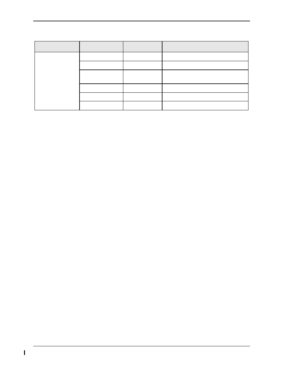
RS8234
14.0 SAR Initialization - Example Tables
ATM ServiceSAR Plus with xBR Traffic Management
14.3 Reassembly Initialization
28234-DSH-001-B
Mindspeed Technologies
TM
14-15
RSM_PM Table Entry
0
BCNT
0x0
Must be initialized to zero.
BIP16
0x0
Must be initialized to zero.
MSN
0x4
First expected MSN in forward monitoring cell is
four.
Rsvd
0x0
Must be initialized to zero.
TRCC0
0x0
Must be initialized to zero.
TRCC01
0x0
Must be initialized to zero.
Table 14-8. Table of Values for Reassembly SAR Shared Memory Initialization (4 of 4)
Table
Field
Initialized Value
Notes

14.0 SAR Initialization - Example Tables
RS8234
14.4 General Initialization
ATM ServiceSAR Plus with xBR Traffic Management
14-16
Mindspeed Technologies
TM
28234-DSH-001-B
14.4 General Initialization
14.4.1 General Control Registers
Before the SAR is enabled, the host must allocate and initialize all of the general
SAR control registers.
Table 14-9
lists the initial value(s) for each field.
Table 14-9. Table of Values for General Control Register Initialization (1 of 3)
Register
Field
Initialized
Value
Notes
CONFIG0
(Configuration Register 0)
LP_ENABLE
0
Local processor not used.
GLOBAL_RESET
0-1
This must be toggled to a logic high and
back to a logic low after completion of all
initialization, but before RSM and SEG
coprocessors are enabled.
PCI_MSTR_RESET
0
Use GLOBAL_RESET to reset SAR.
PCI_ERR_RESET
0
Must be initialized to zero.
INT_LBANK
0-1
Should be set to zero during initialization,
but set to one after system reset.
PCI_READ_MULTI
1
PCI Read Multiple Command used.
PCI_ARB
1
Round robin arbitration of internal
read/write PCI master.
STATMODE
0x0
Selects BOM sync hardware mode.
FR_RMODE
0
Early RSM header processing enabled.
FR_LOOP
0
Internal ATM physical interface disabled.
UTOPIA_MODE
1
Cell handshake mode selected.
LP_BWAIT
0
Selects zero wait states between
consecutive data cycles during local
processor.
MEMCTRL
0
Selects zero wait states SAR shared
memory.
BANKSIZE
0x3
512 KB banks selected.
DIVIDER
0x0
Divide by 128 selected for CLOCK prescaler.
Rsvd
0x0
Must be initialized to zero.

RS8234
14.0 SAR Initialization - Example Tables
ATM ServiceSAR Plus with xBR Traffic Management
14.4 General Initialization
28234-DSH-001-B
Mindspeed Technologies
TM
14-17
INT_DELAY
(Interrupt Delay Register)
TIMER_LOC
0
Interrupt hold-off timer used with HINT*.
EN_TIMER
0
Disable status queue interrupt timer delay.
EN_STAT_CNT
1
Enable status queue interrupt counter delay.
STAT_CNT[7:0]
0x35
Interrupt delay counter set to 53.
HOST_ST_WR
(Host Status Write Register)
RSM_HS_WRITE
--
Read twice after SAR reset.
RSM_LS_WRITE
--
Read twice after SAR reset.
HOST_ISTAT1
(Host Interrupt Status Register
1)
(ALL)
--
Read twice HOST_ST_WR reset.
HOST_ISTAT0
(Host Interrupt Status Register
0)
(ALL)
--
Read twice HOST_ISTAT1 reset.
LP_ISTAT1
(Local Interrupt Status Register
1)
(ALL)
--
Read twice SAR reset.
LP_ISTAT0
(Local Interrupt Status Register
0)
(ALL)
--
Read twice LP_ISTAT1 reset.
HOST_IMASK1
(Host Interrupt Mask Register
1)
(ALL)
0x8700FC07
Enable all errors to cause an interrupt.
HOST_IMASK0
(Host Interrupt Mask Register
0)
(ALL)
0x4040000F
Enable interrupts in errors, counter
relievers and framer interrupt.
LP_IMASK1
(Local Interrupt Mask Register
1)
(ALL)
0x0
Local processor not used.
LP_IMASK0
(Local Interrupt Mask Register
0)
(ALL)
0x0
Local processor not used.
PCI Configuration Space
COMMAND
0x0346
Enable all functions of PCI interface.
LAT_TIMER
0x10
Latency timer = 16 clock periods.
BASE_ADDRESS_
REGISTER_0
0x01
Base address of SAR device in PCI memory
space is 0x0100_0000.
INTERRUPT_LINE
0x00
Interrupt vector = 0.
(ALL OTHER FIELDS)
--
Hard-coded reads only.
Table 14-9. Table of Values for General Control Register Initialization (2 of 3)
Register
Field
Initialized
Value
Notes

14.0 SAR Initialization - Example Tables
RS8234
14.4 General Initialization
ATM ServiceSAR Plus with xBR Traffic Management
14-18
Mindspeed Technologies
TM
28234-DSH-001-B
PCI COMMAND Register
FB_EN
1
Enable master fast back-to-back across
target.
SE_EN
1
Enable SERR* output pin.
PE_EN
1
Enable parity error detection and report.
M_EN
1
Enable RS8234 device master on the PCI
bus.
MS_EN
1
Enable RS8234 memory space access
across the PCI bus.
PCI STATUS Register
(No initialization required.)
PCI SPECIAL_STATUS Register
(No initialization required.)
PCI EEPROM Register
(No initialization required.)
Table 14-9. Table of Values for General Control Register Initialization (3 of 3)
Register
Field
Initialized
Value
Notes

28234-DSH-001-B
Mindspeed Technologies
TM
15-1
15
15.0 Electrical and Mechanical
Specifications
15.1 Timing
15.1.1 PCI Bus Interface Timing
All PCI bus interface signals are synchronous to the PCI bus clock, HCLK, except for HRST* and HINT*.
Table 15-1
provides the PCI bus interface timing parameters.
Figure 15-1
and
Figure 15-2
illustrate this timing.
Table 15-1. PCI Bus Interface Timing Parameters (1 of 2)
Symbol
Parameter
Min
Max
Units
t
cyc
HCLK Cycle Time
(1)
30
--
ns
t
high
HCLK High Time
(1)
11
19
ns
t
low
HCLK Low Time
(1)
11
19
ns
t
su
HAD Input Setup Time to HCLK
(1)
7
--
ns
HC/BE Input Setup Time to HCLK
(1)
7
--
ns
HPAR Input Setup Time to HCLK
(1)
7
--
ns
HFRAME* Input Setup Time to HCLK
(1)
7
--
ns
HIRDY* Input Setup Time to HCLK
(1)
7
--
ns
HTRDY* Input Setup Time to HCLK
(1)
7
--
ns
HSTOP* Input Setup Time to HCLK
(1)
7
--
ns
HDEVSEL* Input Setup Time to HCLK
(1)
7
--
ns
HIDSEL Input Setup Time to HCLK
(1)
7
--
ns
HGNT* Input Setup Time to HCLK
(1)
10
--
ns
HPERR* Input Setup Time to HCLK
(1)
7
--
ns
t
h
Input Hold Time from HCLK�All Inputs
(1)
0
--
ns
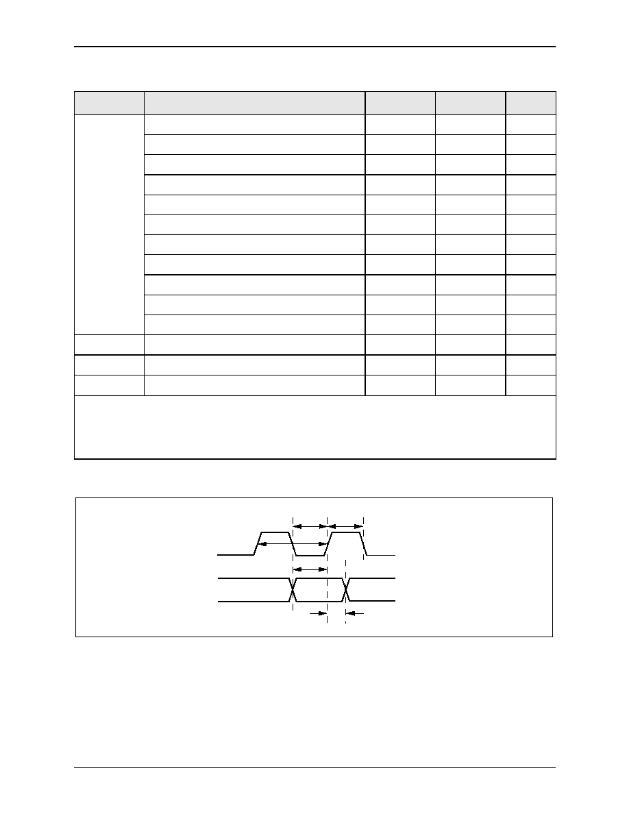
15.0 Electrical and Mechanical Specifications
RS8234
15.1 Timing
ATM ServiceSAR Plus with xBR Traffic Management
15-2
Mindspeed Technologies
TM
28234-DSH-001-B
t
val
HCLK to HAD Valid Delay
(2)
2
11
ns
HCLK to HC/BE Valid Delay
(2)
2
11
ns
HCLK to HPAR Valid Delay
(2)
2
11
ns
HCLK to HFRAME* Valid Delay
(2)
2
11
ns
HCLK to HIRDY* Valid Delay
(2)
2
11
ns
HCLK to HSTOP* Valid Delay
(2)
2
11
ns
HCLK to HDEVSEL Valid Delay
(2)
2
11
ns
HCLK to HPERR* Valid Delay
(2)
2
11
ns
HCLK to HREQ Valid Delay
(2)
2
12
ns
HCLK to HSERR* Valid Delay
(2)
2
11
ns
HCLK to STAT Valid Delay
(3)
2
20
ns
t
on
Float to Active Delay--All Three-state Outputs
(2)
2
--
ns
t
off
Active to Float Delay--All Three-state Outputs
(2)
--
28
ns
t
rst-off
Reset Active to Output Float Delay
--
40
ns
NOTE(S):
(1)
See
Figure 15-1
for waveforms and definitions.
(2)
See
Figure 15-2
for waveforms and definitions. The maximum output delays are measured with a 50 pF load and the
minimum delays are measured with a 0 pF load.
(3)
Applicable when STAT outputs configured as BOM cell synchronization signals.
Figure 15-1. PCI Bus Input Timing Measurement Conditions
Table 15-1. PCI Bus Interface Timing Parameters (2 of 2)
Symbol
Parameter
Min
Max
Units
HCLK
Input
t
low
t
high
t
cyc
t
su
t
h
100074_087

RS8234
15.0 Electrical and Mechanical Specifications
ATM ServiceSAR Plus with xBR Traffic Management
15.1 Timing
28234-DSH-001-B
Mindspeed Technologies
TM
15-3
15.1.2 ATM Physical Interface Timing--UTOPIA and Slave UTOPIA
All ATM physical interface signals are synchronous to the interface clock, FRCTRL, except for TXCLAV and
RXCLAV in the slave UTOPIA mode. Timing parameters for the UTOPIA interface are provided in
Table 15-2
.
Table 15-3
provides the timing parameters for the slave UTOPIA interface. Timing diagrams for both interfaces
are provided in
Figure 15-3
and
Figure 15-4
.
Figure 15-2. PCI Bus Output Timing Measurement Conditions
Table 15-2. UTOPIA Interface Timing Parameters (1 of 2)
Symbol
Parameter
Min
Max
Units
t
cyc
FRCTRL Cycle Time
(1)
30
--
ns
t
high
FRCTRL High Time
(1)
(% of tcyc)
40
60
%
t
low
FRCTRL Low Time
(1)
(% of tcyc)
40
60
%
t
su
RXD Input Setup Time to FRCTRL
(1)
10
--
ns
RXPAR Input Setup Time to FRCTRL
(1)
10
--
ns
RXSOC Input Setup Time to FRCTRL
(1)
10
--
ns
RXCLAV Input Setup Time to FRCTRL
(1)
10
--
ns
TXCLAV Input Setup Time to FRCTRL
(1)
10
--
ns
t
h
RXD Input Hold Time from FRCTRL
(1)
1
--
ns
RXPAR Input Hold Time from FRCTRL
(1)
1
--
ns
RXSOC Input Hold Time from FRCTRL
(1)
1
--
ns
RXCLAV Input Hold Time from FRCTRL
(1)
1
--
ns
TXCLAV Input Hold Time from FRCTRL
(1)
1
--
ns
HCLK
Output Delay
Three-state Output
tval
t
on
toff
100074_088
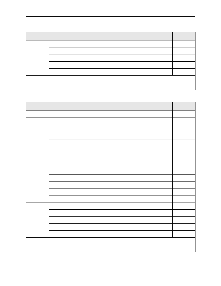
15.0 Electrical and Mechanical Specifications
RS8234
15.1 Timing
ATM ServiceSAR Plus with xBR Traffic Management
15-4
Mindspeed Technologies
TM
28234-DSH-001-B
t
val
FRCTRL to TXD Valid Delay
(2)
2
18
ns
FRCTRL to TXPAR Valid Delay
(2)
2
18
ns
FRCTRL to TXSOC Valid Delay
(2)
2
18
ns
FRCTRL to TXEN* Valid Delay
(2)
2
20
ns
FRCTRL to RXEN* Valid Delay
(2l
2
20
ns
NOTE(S):
(1)
See
Figure 15-3
for waveforms and definitions.
(2)
See
Figure 15-4
for waveforms and definitions. The output delays are measured with a 25 pF load.
Table 15-3. Slave UTOPIA Interface Timing Parameters
Symbol
Parameter
Min
Max
Units
t
cyc
FRCTRL Cycle Time
(1)
30
--
ns
t
high
FRCTRL High Time
(1)
(% of tcyc)
40
60
%
t
low
FRCTRL Low Time
(1)
(% of tcyc)
40
60
%
t
su
RXD Input Setup Time to FRCTRL
(1)
6
--
ns
RXPAR Input Setup Time to FRCTRL
(1)
3
--
ns
RXSOC Input Setup Time to FRCTRL
(1)
8
--
ns
RXEN* Input Setup Time to FRCTRL
(1)
10
--
ns
TXEN* Input Setup Time to FRCTRL
(1)
3
--
ns
t
h
RXD Input Hold Time from FRCTRL
(1)
1
--
ns
RXPAR Input Hold Time from FRCTRL
(1)
1
--
ns
RXSOC Input Hold Time from FRCTRL
(1)
1
--
ns
RXEN* Input Hold Time from FRCTRL
(1)
1
--
ns
TXEN* Input Hold Time from FRCTRL
(1)
1
--
ns
t
val
FRCTRL to TXD Valid Delay
(2)
2
16
ns
FRCTRL to TXPAR Valid Delay
(2)
2
16
ns
FRCTRL to TXCLAV Valid Delay
(2)
2
20
ns
FRCTRL to RXCLAV Valid Delay
(2)
2
20
ns
FRCTRL to TXSOC Valid Delay
(2)
2
17
ns
NOTE(S):
(1)
See
Figure 15-3
for waveforms and definitions.
(2)
See
Figure 15-4
for waveforms and definitions. The output delays are measured with a 25 pF load.
Table 15-2. UTOPIA Interface Timing Parameters (2 of 2)
Symbol
Parameter
Min
Max
Units
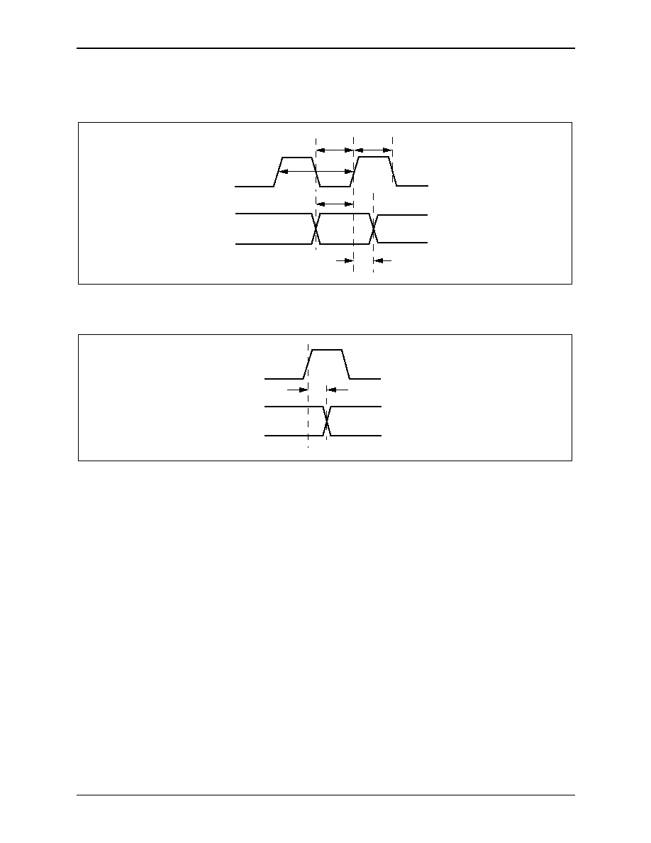
RS8234
15.0 Electrical and Mechanical Specifications
ATM ServiceSAR Plus with xBR Traffic Management
15.1 Timing
28234-DSH-001-B
Mindspeed Technologies
TM
15-5
Figure 15-3. UTOPIA and Slave UTOPIA Input Timing Measurement Conditions
Figure 15-4. UTOPIA and Slave UTOPIA Output Timing Measurement Conditions
FRCTRL
Input
tlow
thigh
tcyc
tsu
th
100074_089
FRCTRL
Output Delay
tval
100074_090

15.0 Electrical and Mechanical Specifications
RS8234
15.1 Timing
ATM ServiceSAR Plus with xBR Traffic Management
15-6
Mindspeed Technologies
TM
28234-DSH-001-B
15.1.3 System Clock Timing
The system clock timing consists of the CLK2X input and the SYSCLK and CLKD3 outputs. The CLK2X
input and SYSCLK outputs are used to generate the internal and external system clocks, as well as SAR shared
memory and processor read and write timing. The CLKD3 output can be used as the ATM physical interface
clock. There is no defined skew relationship between the CLK2X input and SYSCLK and CLKD3 outputs.
Table 15-4
specifies the timing parameters of the three clocks.
Figure 15-5
and
Figure 15-6
illustrates this
timing.
Table 15-4. System Clock Timing
Symbol
Parameter
Min
Max
Units
Input Clocks
(1)
t
cf
CLK2X Frequency
0
66
MHz
t
c
CLK2X Period
15.15
ns
t
cd
CLK2X Duty Cycle
40
60
%
t
cr
CLK2X Rise Time
0
6
ns
t
cf
CLK2X Fall Time
0
6
ns
Output Clocks
(2)
t
sf
SYSCLK Frequency
t
CF
/2
MHz
t
s
SYSCLK Period
2t
C
ns
t
sh
SYSCLK High Time
(t
S
/2) � 2
(t
S
/2) + 2
ns
t
sl
SYSCLK Low Time
(t
S
/2) � 2
(t
S
/2) + 2
ns
t
sr
SYSCLK Rise Time
1
4
ns
t
sf
SYSCLK Fall Time
1
4
ns
t
df
CLKD3 Frequency
t
CF
/3
MHz
t
d
CLKD3 Period
3t
C
t
dh
CLKD3 High Time
(t
D
/2) � 2
(t
D
/2) + 2
ns
t
dl
CLKD3 Low Time
(t
D
/2) � 2
(t
D
/2) + 2
ns
t
dr
CLKD3 Rise Time
1
4
ns
t
df
CLKD3 Fall Time
1
4
ns
NOTE(S):
(1)
See
Figure 15-5
for waveforms and definitions.
(2)
See
Figure 15-6
for waveforms and definitions. The outputs are measured with a load of 35 pF.
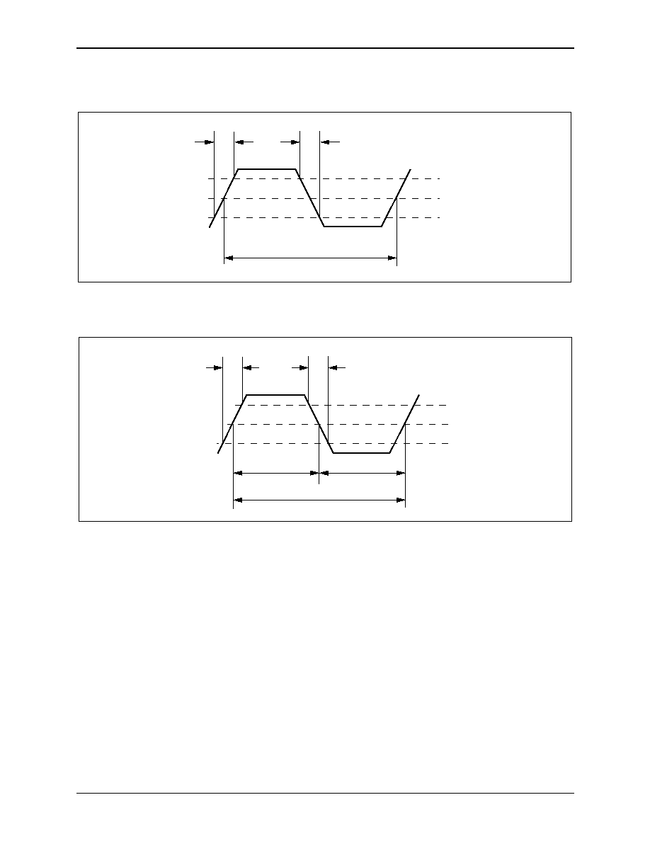
RS8234
15.0 Electrical and Mechanical Specifications
ATM ServiceSAR Plus with xBR Traffic Management
15.1 Timing
28234-DSH-001-B
Mindspeed Technologies
TM
15-7
Figure 15-5. Input System Clock Waveform
Figure 15-6. Output System Clock Waveform
tcr
tcf
2.0 V
1.5 V
0.8 V
tc
100074_091
tsr,t dr
tsf,t df
2.4 V
1.5 V
0.4 V
tsh,t dh
tsl,t dl
ts,t d
100074_092

15.0 Electrical and Mechanical Specifications
RS8234
15.1 Timing
ATM ServiceSAR Plus with xBR Traffic Management
15-8
Mindspeed Technologies
TM
28234-DSH-001-B
15.1.4 RS8234 Memory Interface Timing
Memory access times and other timing requirements are specified at three typical implementations of one, two,
and four banks of by_8 SRAM.
Table 15-5
gives the number of loads per bank for the different SRAM
organizations while
Table 15-6
gives the capacitive loading used in the timing specifications given for the three
typical implementations. RS8234 memory interface timing is given in
Table 15-7
. See
Section 9.2
for details of
memory bank organization.
Table 15-5. SRAM Organization Loading Dependencies
Signal
Loads/Bank
(1)
by_16 SRAM
by_8 SRAM
by_4 SRAM
LADDR[18:0]
(1)
2
4
8
LDATA[31:0]
(1)
1
1
1
MWR*
(1)
2
N/A
N/A
MOE*
(1)
2
4
8
MCSx*
(1, 2)
2
4
8
MWEx*
(1)
1
1
2
NOTE(S):
(1)
Typical input loading for SRAM is 7 pF. For exact values, consult the SRAM databook.
(2)
Only connected to one bank by definition.
Table 15-6. SAR Shared Memory Output Loading Conditions
Signal
4 banks of by_8
SRAM
2 banks of by_8
SRAM
1 bank of
by_8 SRAM
Units
Memory Interface Loading
(1)
LADDR[18:0]
(1)
150
100
50
pF
MOE*
150
100
50
pF
MWR*
(2)
--
50
35
pF
LDATA[31:0]
50
35
25
pF
MWE[3:0]*
50
35
25
pF
MCS[3:0]*
50
35
25
pF
NOTE(S):
(1)
In general, the LADDR loading is the most critical parameter, one bank of by_8 SRAM has the same address loading as two
banks of by_16 and 1/2 bank of by_4 SRAM. For example, use the timing from the two banks of by_8 column for four banks
of by_16 SRAM, or one bank of by_4 SRAM.
(2)
For by_16 SRAM, the WE* input has the same loading as the address bus and OE*; therefore, 16 loads specified by the four
banks of by_8 is not applicable, since the maximum number of by_16 SRAMs supported is eight.

RS8234
15.0 Electrical and Mechanical Specifications
ATM ServiceSAR Plus with xBR Traffic Management
15.1 Timing
28234-DSH-001-B
Mindspeed Technologies
TM
15-9
Table 15-7. RS8234 Memory Interface Timing
Symbol
Parameter
4 banks of
by_8 SRAM
2 banks of
by_8 SRAM
1 bank of by_8
SRAM
Units
Min
Max
Min
Max
Min
Max
Memory Read Timing
t
rc
READ Cycle Time
(2)
T
T
T
ns
t
aov
LADDR[18:0] Output Valid
(1)
1
10
1
8
1
7
ns
t
mcsov
MCS[3:0]* Output Valid
(1)
1
10
1
8
1
7
ns
t
mweov
MWE* Byte Enables Output Valid
(1)
(RAMMODE = 1)
1
10
1
8
1
7
ns
t
moel
MOE* Low
(1)
17
16
15
ns
t
moeh
MOE* High
(1)
10
8
7
ns
t
dod
LDATA Output Disable
(1)
7
6
6
ns
t
dis
LDATA Input Setup
(1)
5
5
5
ns
t
dh
LDATA Input Hold
(1)
0
0
0
ns
t
doe
LDATA Driven by SAR
(1)
12
11
11
ns
t
dodmoe
LDATA Disable to MOE* Low
(1)
0
0
0
ns
t
moedoe
MOE* High to LDATA Driven
(1)
6
7
8
ns
Memory Write Timing
t
wc
WRITE Cycle Time
(2)
T
T
T
ns
t
w
MWR*, MWE[3:0]* Width
(2, 4)
T/2-2
T/2-2
T/2-2
ns
t
aov
LADDR[18:0] Output Valid
(4)
1
10
1
8
1
7
ns
t
mcsov
MCS[3:0]* Output Valid
(4)
1
10
1
8
1
7
ns
t
mweov
MWE* Byte Enables Output Valid
(1)
(RAMMODE = 1)
1
10
1
8
1
7
ns
t
dov
LDATA Output Valid
( 4)
1
10
1
10
1
10
ns
t
mwel
MWE[3:0]* Low
(4)
T/2-2
16
16
16
ns
t
mweh
MWE[3:0]* High
(4)
1
1
1
ns
t
mwrl
MWR[3:0]* Low
( 4)
T/2-2
16
16
16
ns
t
mwrh
MWR[3:0]* High
(4)
1
1
1
ns
NOTE(S):
(1)
See
Figure 15-7
for waveforms.
(2)
T = t
s
for single cycle memory (no wait states), T = 2t
s
for two cycle memory, (one wait state).
(3)
Insert one clock cycle for two cycle memory (one wait state).
(4)
See
Figure 15-8
for waveforms.
(5)
SYSCLK shown for reference only.
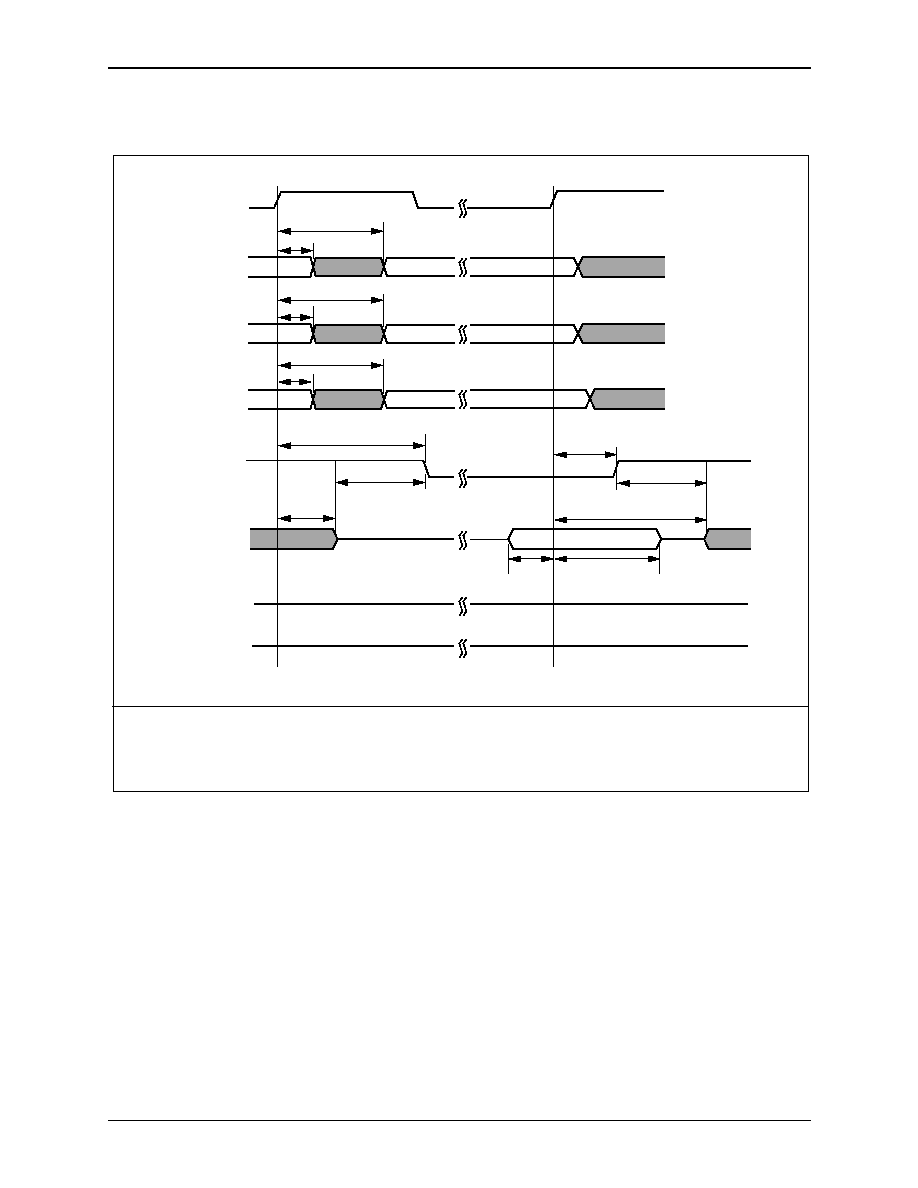
15.0 Electrical and Mechanical Specifications
RS8234
15.1 Timing
ATM ServiceSAR Plus with xBR Traffic Management
15-10
Mindspeed Technologies
TM
28234-DSH-001-B
Figure 15-7. RS8234 Memory Read Timing
LADDR
MWE[3:0]* BE*
MOE*
MCS[3:0]*
taov(max)
SYSCLK
taov(min)
tmcsov
mweov(max)
mweov(min)
(max)
tmcsov(min)
tmoel
tdod
tdis
tdh
t
t
moeh
moedoe
SRAM Data Valid
VALID
VALID
(1)
LDATA
t dodmoe
t
t
VALID
tdoe
(2)
MWE*
MWR*
8236_117
NOTE(S):
(1)
Insert one clock cycle for two cycle memory (one wait state).
(2)
SYSCLK shown for reference only.
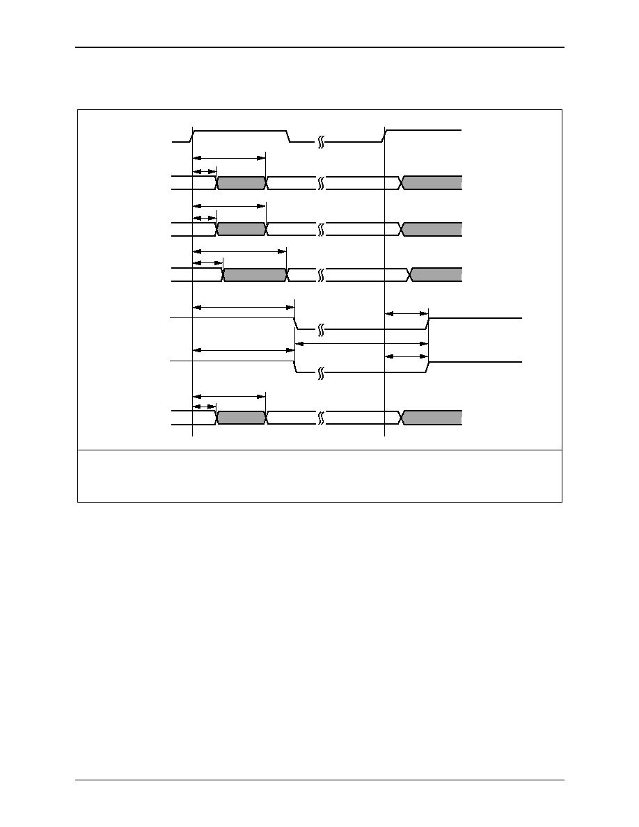
RS8234
15.0 Electrical and Mechanical Specifications
ATM ServiceSAR Plus with xBR Traffic Management
15.1 Timing
28234-DSH-001-B
Mindspeed Technologies
TM
15-11
Figure 15-8. RS8234 Memory Write Timing
LADDR
LDATA
MWE[3:0]*
MCS[3:0]*
taov(max)
SYSCLK
taov(min)
tmcsov(max)
tmcsov(min)
tmweov(max)
tmweov(min)
tmwel
tmweh
VALID
VALID
VALID
(1)
MWR*
tmwrl
tmwrh
tdov(max)
tdov(min)
tw
VALID
(2)
MWE[3:0]* BE*
100074_094
NOTE(S):
(1)
Insert 1 clock cycle for 2-cycle memory (1 wait state).
(2)
SYSCLK shown for reference only.
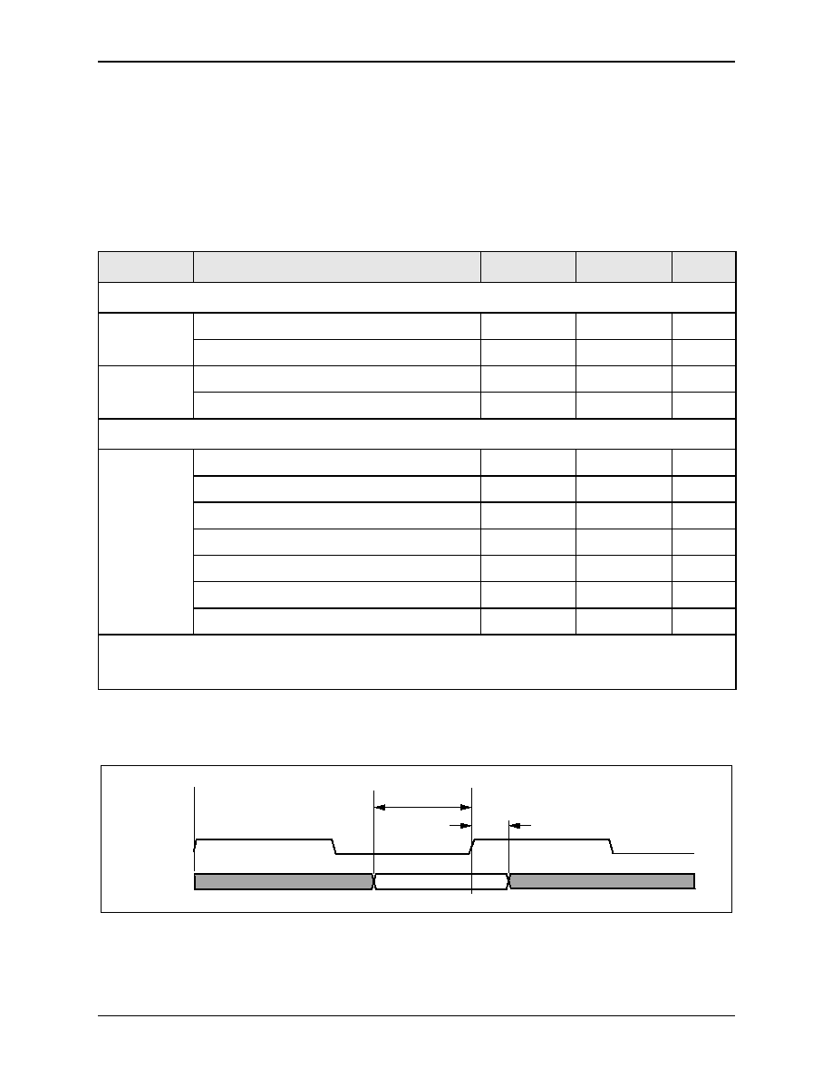
15.0 Electrical and Mechanical Specifications
RS8234
15.1 Timing
ATM ServiceSAR Plus with xBR Traffic Management
15-12
Mindspeed Technologies
TM
28234-DSH-001-B
15.1.5 PHY Interface Timing (Standalone Mode)
The standalone mode of operation is entered when the PROCMODE input is at a logic high indicating that no
local processor is present. In this mode, the RS8234 changes its memory map to include the ATM physical
interface device. The interface is fully synchronous to SYSCLK and is designed to interface directly to the
RS825x ATM Receiver/Transmitter. Timing is given in
Table 15-8
,
Figure 15-9
, and
Figure 15-10
. See
Section 10.6
or details.
Table 15-8. PHY Interface Timing (PROCMODE = 1)
Symbol
Parameter
Min
Max
Units
Synchronous Inputs
t
is
PWAIT* Input Setup
(1)
14
ns
LDATA Input Setup
(1)
5
ns
t
ih
PWAIT* Input Hold
(1)
0
ns
LDATA Input Hold
(1)
0
ns
Synchronous Outputs
t
ov
PRDY* Output Valid Delay
(2)
5
15
ns
PAS Output Valid Delay
(2)
5
15
ns
PCS* Output Valid Delay
(2)
5
15
ns
PBLAST* Output Valid Delay
(2)
5
15
ns
PWNR Output Valid Delay
(2)
5
15
ns
LDATA* Output Valid Delay
(2)
1
10
ns
LADDR Output Valid Delay
(2)
1
10
ns
NOTE(S):
(1)
See
Figure 15-9
for waveforms and definitions.
(2)
See
Figure 15-10
for waveforms and definitions. The outputs are measured with a load of 35 pF.
Figure 15-9. Synchronous PHY Interface Input Timing
tih
SYSCLK
Sync Input
tis
100074_095
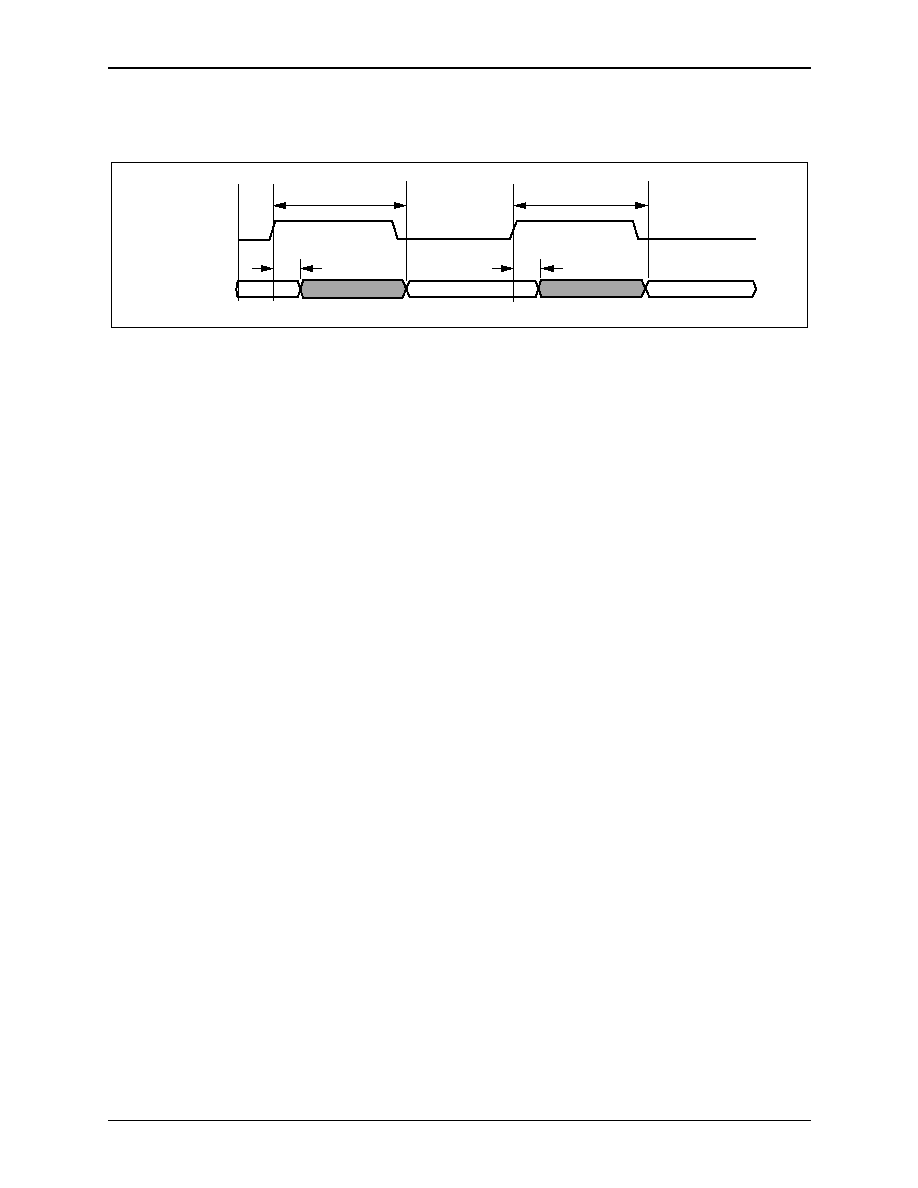
RS8234
15.0 Electrical and Mechanical Specifications
ATM ServiceSAR Plus with xBR Traffic Management
15.1 Timing
28234-DSH-001-B
Mindspeed Technologies
TM
15-13
Figure 15-10. Synchronous PHY Interface Output Timing
t ov (min)
SYSCLK
Sync Output
t ov (max)
t ov (min)
t ov (max)
VALID
VALID
100074_096

15.0 Electrical and Mechanical Specifications
RS8234
15.1 Timing
ATM ServiceSAR Plus with xBR Traffic Management
15-14
Mindspeed Technologies
TM
28234-DSH-001-B
15.1.6 Local Processor Interface Timing
Timing for the local processor interface can be broken into two sections. The first is the synchronous to
SYSCLK interface of processor control signals to and from the RS8234. The second is the interface to the SAR
shared memory and the RS8234 control and status registers, which involves both SRAM and transceiver, as well
as buffer timing parameters that are not specified and are left up to the system designer.
All of the synchronous interface signals are inputs to the RS8234 except for SYSCLK and the ready output
of the RS8234 (PRDY*). The output loading of these signals is 35 pF for the timing given in
Table 15-9
.
Memory Interface Timing is given in
Table 15-10
.
Table 15-9. Synchronous Processor Interface Timing
Symbol
Parameter
Min
Max
Units
Synchronous Inputs
t
is
PCS* Input Setup
(1)
8
ns
PAS* Input Setup
(1)
10
ns
PBLAST* Input Setup
(1)
10
ns
PWAIT* Input Setup
(1)
10
ns
PADDR[1,0] Input Setup
(1)
10
ns
PBSEL[1,0] Input Setup
(1)
8
ns
PBE[3:0]* Input Setup
(1)
8
ns
PWNR Input Setup
(1)
10
ns
t
ih
PCS* Input Hold
(1)
0
ns
PAS* Input Hold
(1)
0
ns
PBLAST* Input Hold
(1)
0
ns
PWAIT* Input Hold
(1)
0
ns
PADDR[1,0] Input Hold
(1)
0
ns
PBSEL[1,0] Input Hold
(1)
0
ns
PBE[3:0]* Input Hold
(1)
0
ns
PWNR Input Hold
(1)
0
ns
Synchronous Outputs
t
ov
PRDY* Output Valid Delay
(2)
5
15
ns
NOTE(S):
(1)
See
Figure 15-11
for waveforms and definitions.
(2)
See
Figure 15-12
for waveforms and definitions. The outputs are measured with a load of 35 pF.
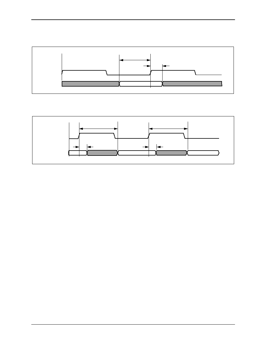
RS8234
15.0 Electrical and Mechanical Specifications
ATM ServiceSAR Plus with xBR Traffic Management
15.1 Timing
28234-DSH-001-B
Mindspeed Technologies
TM
15-15
Figure 15-11. Synchronous Local Processor Input Timing
Figure 15-12. Synchronous Local Processor Output Timing
tih
SYSCLK
Sync Input
tis
100074_097
t ov (min)
SYSCLK
Sync Output
t ov (max)
t ov (min)
t ov (max)
VALID
VALID
100074_098

15.0 Electrical and Mechanical Specifications
RS8234
15.1 Timing
ATM ServiceSAR Plus with xBR Traffic Management
15-16
Mindspeed Technologies
TM
28234-DSH-001-B
Table 15-10. Local Processor Memory Interface Timing
Symbol
Parameter
Min
Max
Units
t
pdaenl
SYSCLK to PDAEN* Low, Bus Recovery Cycle
(1)
12
ns
t
pdaenh
SYSCLK to PDAEN* High, Bus Recovery Cycle
(1)
2
ns
t
lod
LADDR[18:2], LDATA Output Disable to PDAEN* Low,
Bus Recovery Cycle
(1)
4
ns
t
loe
PDAEN* High to LADDR[18:2], LDATA Output Enable,
Bus Recovery Cycle
(1)
9
ns
t
mcs
SYSCLK to MCS*[3:0] Valid
(1)
1
6
ns
t
lav
SYSCLK to LADDR[1,0] Valid
(1, 2)
1
7
ns
t
oel
MOE* Active from SYSCLK
(1, 3)
8
20
ns
t
oeh
MOE* Inactive from SYSCLK
(1, 3)
1
10
ns
t
wl
MWR*, MWE[3:0] Active from SYSCLK
(1, 3)
16
ns
t
wh
MWR*, MWE[3:0]* Inactive to SYSCLK
(1, 3)
1
ns
t
be
MWE[3:0]* Byte Enables Valid from SYSCLK (RAMMODE = 1)
(1)
1
7
ns
t
crd
CSR Read Data Output Valid
2
20
ns
t
cwds
CSR Write Data Setup to SYSCLK
8
ns
t
cwdh
CSR Write Data Hold from SYSCLK
0
ns
t
las
LADDR Setup to SYSCLK
12
ns
NOTE(S):
(1)
See
Figure 15-13
and
Figure 15-14
for waveforms and definitions.
(2)
t
lav
is valid for second and subsequent accesses during burst transfers. See functional timing diagrams.
(3)
In the case of two cycle memory, or when inserting wait states by PWAIT*, MOE*, MWE[3:0]*, and MWR* are
extended across two or more clock cycles with the same relative timing to SYSCLK. See the functional timing diagrams in
Section 10.6
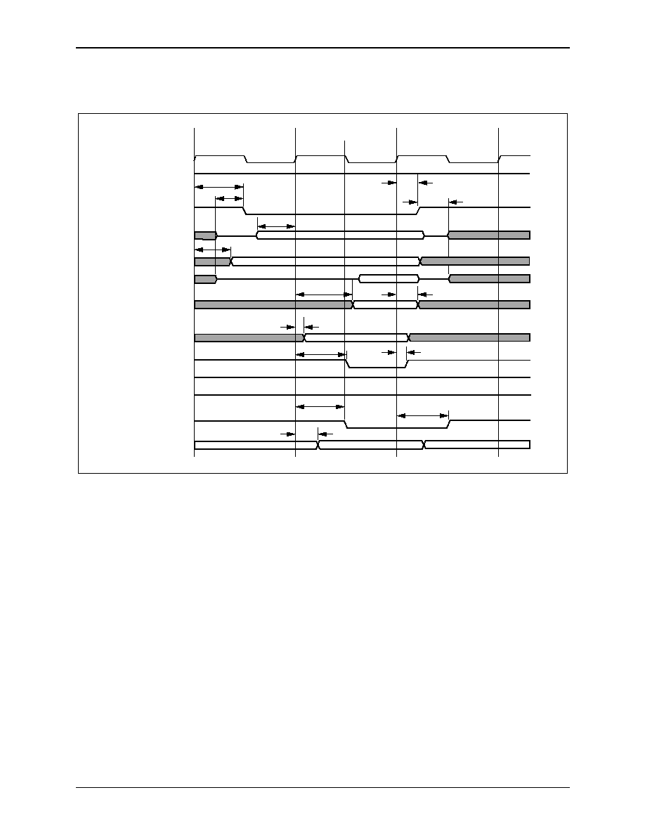
RS8234
15.0 Electrical and Mechanical Specifications
ATM ServiceSAR Plus with xBR Traffic Management
15.1 Timing
28234-DSH-001-B
Mindspeed Technologies
TM
15-17
Figure 15-13. Local Processor Read Timing
tmcs
tpdaenh
toeh
tlod
tloe
tpdaenl
tlav
tcrd(min)
SYSCLK
PWAIT*
PDAEN*
LADDR[18:2]
LADDR[1:0]
LDATA (RAM Read)
LDATA (CSR or
MCS[3:0]*
MOE*
MWE[3:0]*
MWR*
PRDY*
lp addr
t be
MWE[3:0]* BE
tov
tcrd(max)
toel
toh
Int. Mem. Read)
tlas
100074_099
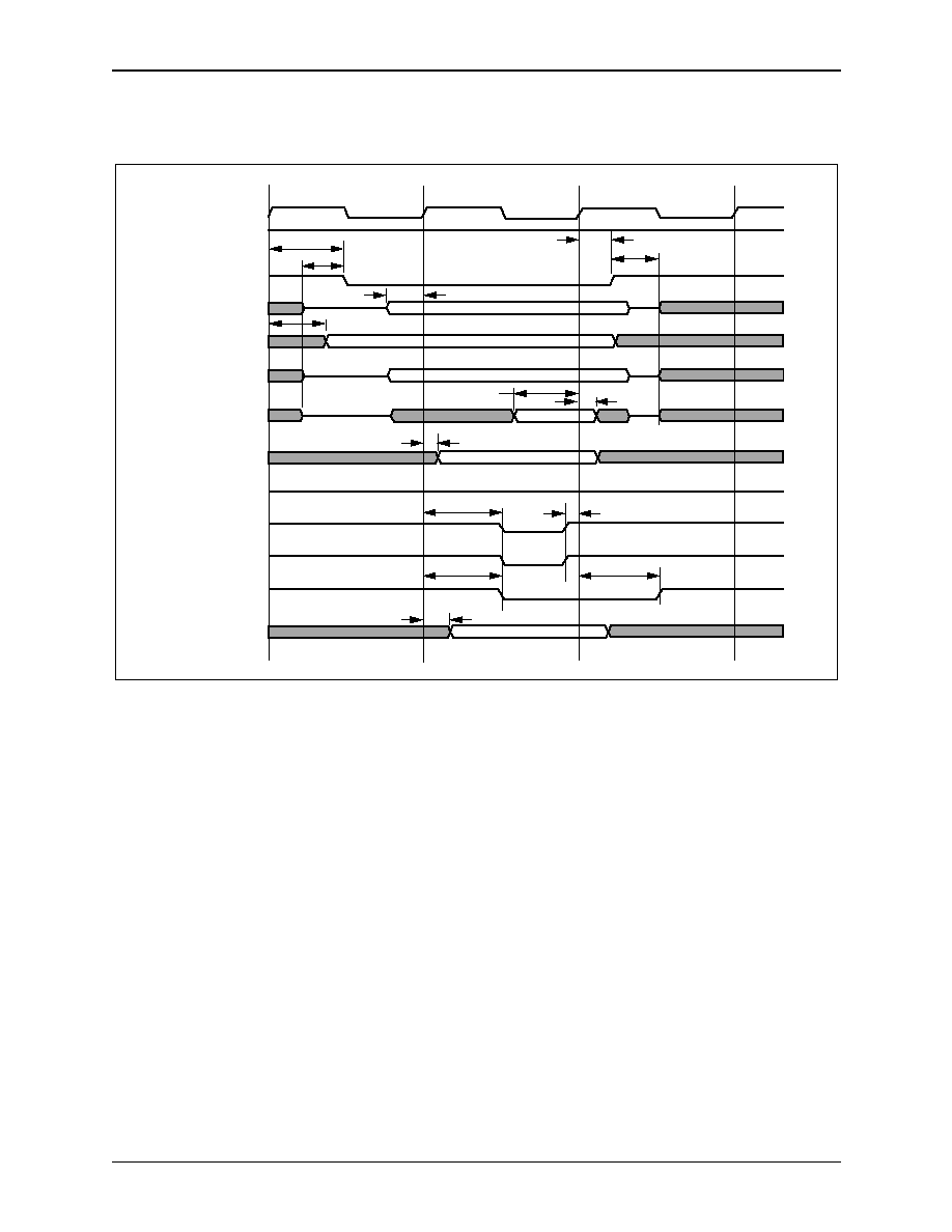
15.0 Electrical and Mechanical Specifications
RS8234
15.1 Timing
ATM ServiceSAR Plus with xBR Traffic Management
15-18
Mindspeed Technologies
TM
28234-DSH-001-B
Figure 15-14. Local Processor Write Timing
tmcs
tpdaenh
twh
tlod
tpdaenl
tlav
tcwdh
tloe
lp data
SYSCLK
PWAIT*
PDAEN*
LADDR[18:2]
LADDR[1:0]
LDATA (CSR or
LDATA (RAM wr)
MCS[3:0]*
MOE*
MWE[3:0]*
MWE[3:0]* BE
MWR*
PRDY*
lp addr
twl
tov
toh
Int. Mem. write)
tlas
t cwds
100074_100

RS8234
15.0 Electrical and Mechanical Specifications
ATM ServiceSAR Plus with xBR Traffic Management
15.2 Absolute Maximum Ratings
28234-DSH-001-B
Mindspeed Technologies
TM
15-19
15.2 Absolute Maximum Ratings
Stresses above those listed as absolute maximum ratings (
Table 15-11
) can cause permanent damage to the
device. This is a stress rating only and functional operation of the device at these or any other conditions above
those indicated in other sections of this document is not implied. Exposure to absolute maximum rating
conditions for extended periods may affect device reliability. This device should be handled as an ESD-sensitive
device. Voltage on any signal pin exceeding 5.5 V can induce destructive latchup.
Table 15-11. Absolute Maximum Ratings
Parameter
Value
Unit
Supply Voltage (Vdd)
�0.5 to +4
V
Input Voltage
�0.5 to +5.5
V
Output Voltage
�0.5 to (Vdd + 0.3)
V
Storage Temperature
�40 to 125
C
Maximum Current @ Max Clock Frequencies
and 3.6 V
400
mA
Moisture Sensitivity Level (MSL)
4
--
FIT @ 55
�
C
55
--
Theta Ja (T
a
= 85
�
C, T
j
= 125
�
C)
17
C/W

15.0 Electrical and Mechanical Specifications
RS8234
15.3 DC Characteristics
ATM ServiceSAR Plus with xBR Traffic Management
15-20
Mindspeed Technologies
TM
28234-DSH-001-B
15.3 DC Characteristics
Table 15-12. DC Characteristics
Parameter
Conditions
Min
Max
Unit
Operating Supply Voltage (Vdd)
3.0
3.6
V
Output Voltage High
I
OH
= �500 �A V PCI signaling)
0.9*Vdd
V
I
OH
= �2 mA
(for all 5V PCI signaling)
2.4
V
I
OH
= 4.0 mA
(for all other signals)
2.4
V
Output Voltage Low
I
OL
= 1500 �A
(for all 3.3 V PCI signals)
0.1*Vdd
V
I
OH
= 3 mA, 6 mA
(1)
(for all 5V PCI signaling)
0.55
V
I
OL
= 4.0 mA
(for all other signals)
0.4
V
Input Voltage High
(PCI)
(for 3.3 V PCI signaling)
0.5*Vdd
5.25
V
(for 5 V PCI signaling)
2.0
5.25
V
Input Voltage High
(HCLK, CLK2X, HRST*, FRCTRL)
0.7*Vdd
5.25
V
Input Voltage High
(all others)
2.0
5.25
V
Input Voltage Low
(PCI)
(for 3.3 V PCI signaling)
�0.5
0.3*Vdd
V
(for 5 V PCI signaling)
�0.5
0.8
V
Input Voltage Low
(HCLK, CLK2X, HRST*, FRCTRL)
0
0.3*Vdd
V
Input Voltage Low
(all others)
0
0.8
V
Input Leakage Current
Vin = Vdd or GND
�10
10
�
A
Three-state Output Leakage Current
VOUT = Vdd or GND
�10
10
�
A
Pullup Current
30
100
�
A
Input Capacitance
7
pF
Output Capacitance
7
pF
NOTE(S):
All outputs are CMOS drive levels, and can be used with CMOS or TTL logic.
(1)
Per PCI Specification Rev 2.1, signals without pullup resistors must have 3 mA low output current. Signals requiring pullup
must have 6 mA. The latter include: FRAME*, TRDY*, IRDY*, DEVSEL*, STOP*, SERR*, PERR*, and LOCK*.

RS8234
15.0 Electrical and Mechanical Specifications
ATM ServiceSAR Plus with xBR Traffic Management
15.4 Mechanical Specifications
28234-DSH-001-B
Mindspeed Technologies
TM
15-21
15.4 Mechanical Specifications
The RS8234 388-pin BGA package is illustrated in
Figure 15-15
.
Figure 15-16
is a pinout configuration of the
RS8234, and a pin listing is given in
Table 15-13
.
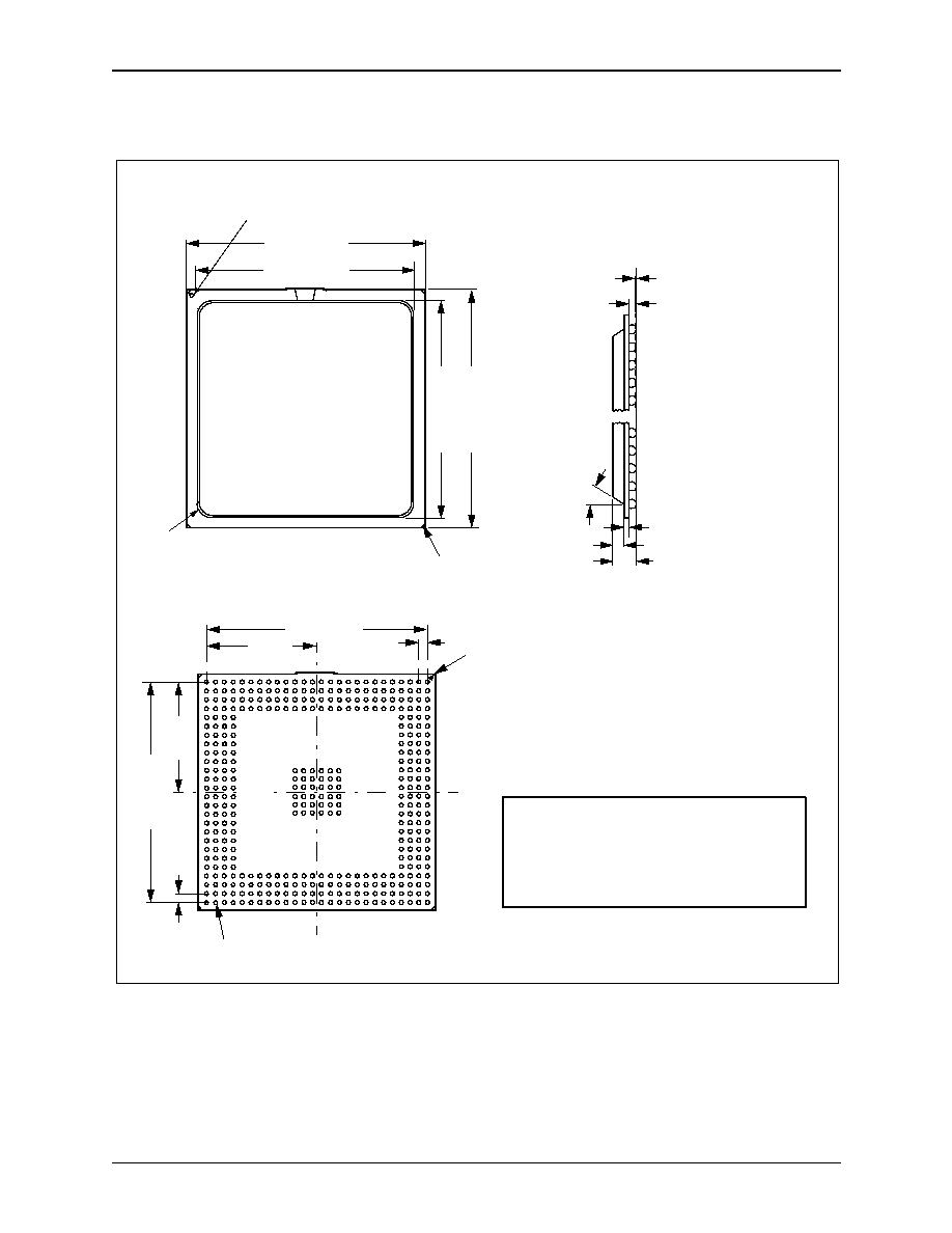
15.0 Electrical and Mechanical Specifications
RS8234
15.4 Mechanical Specifications
ATM ServiceSAR Plus with xBR Traffic Management
15-22
Mindspeed Technologies
TM
28234-DSH-001-B
Figure 15-15. 388-Pin Ball Grid Array Package (BGA)
35.000 � .100
30.000 � .050
35.
000 �
.100
3
0
.00
0 � .05
0
1.70 R
TYP 4 PL
PIN A1
TRIANGLE
(UNDERSIDE)
OPTIONAL
45� CHAMFER
TYP 4 PL
TOP VIEW
15�
2.220 � .220 BEFORE REFLOW
1.100 � .050
.520 � .070
SEATING PLANE
.150 MAX
0.600 � .100 BEFORE REFLOW
SIDE VIEW
2.100 REF AFTER REFLOW
0.480 REF AFTER REFLOW
1.270 TYP
15.875
31.750 BSC
31.
750
B
S
C
1
.
27
0 T
Y
P
15.
875
A
26
25
24
23
22
21
20
19
18
17
16
15
14
13
12
11
10
9
8
7
6
5
4 3
2
1
B
C
D
E
F
G
H
J
K
L
M
N
P
R
T
U
V
W
Y
AA
AB
AC
AD
AE
AF
BOTTOM VIEW
PIN A1
TRIANGLE
0.75 � 0.15 DIA
NOTES:
- ALL DIMENSIONS ARE IN MILLIMETERS (MM).
- REFLOW APPLIES TO SOLDERING TO HOST
PC BOARD.
- REF: GP00-D353
- THERMAL BALLS IN CENTER CONNECT
TO GROUND.
100074_101
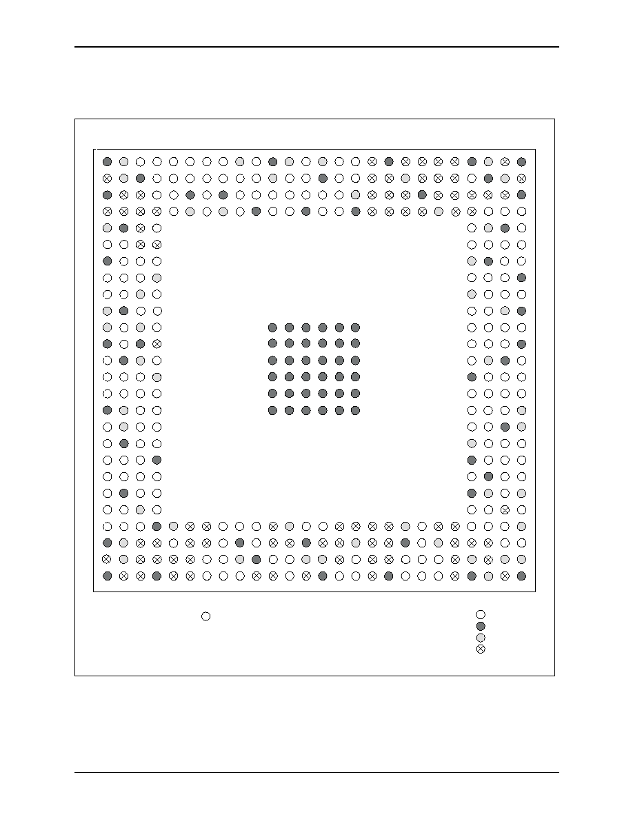
RS8234
15.0 Electrical and Mechanical Specifications
ATM ServiceSAR Plus with xBR Traffic Management
15.4 Mechanical Specifications
28234-DSH-001-B
Mindspeed Technologies
TM
15-23
Figure 15-16. RS8234 Pinout Configuration
STAT0
STAT1
RAMMODE
MWE3_
MWE2_
MWE1_
MWE0_
MOE_
MWR_
MCS3_
MCS2_
MCS1_
MCS0_
HLED_
CLKD3
SYSCLK
CLK2X
LDATA31
LDATA30
LDATA29
LDATA28
LDATA24
LDATA25
LDATA26
LDATA27
LDATA23
LDATA21
LDATA19
LDATA18
LDATA15
LDATA14
LDATA13
LDATA12
LDATA11
LDATA10
LDATA8
LDATA7
LDATA6
LDATA5
LDATA4
LDATA2
LDATA0
VDD
RXPAR
RXD7
RXD6
RXD5
RXD2
RXD1
RXD0
RXSOC
RXEN_
FRCFG0
FRCFG1
FRCTRL
TXEN_
TXCLAV
TXPAR
TXD7
TXD6
TXD5
TXD4
TXD3
TXD2
TXD1
TXD0
TCLK
TRST_
TDI
HINT_
HRST_
HAD30
HAD27
HAD25
HCBE3_
HAD23
HAD22
HAD17
HCBE2_
HCLK
HFRAME*_
HIRDY*_
HTRDY*_
HDEVSEL_
HSTOP_
HPERR_
HSERR_
HPAR
HCBE1_
HAD15
HAD14
HAD13
HAD12
HAD11
HAD10
HAD9
HAD8
HAD7
HAD6
HAD5
HCBE0_
HAD4
HAD3
HAD2
HAD1
HAD0
HENUM
PROCMODE
PRST_
PINT_
PFAIL_
PDAEN_
PCS_
PAS_
PBLAST_
PWAIT_
PRDY_
PWNR
PBE_
PBE2_
PBE1_
PBE0_
PBSEL1
PBSEL0
PADDR1
PADDR0
LADDR18
LADDR17
LADDR16
LADDR15
LADDR14
LADDR13
LADDR12
LADDR11
LADDR10
LADDR9
LADDR8
LADDR7
LADDR6
LADDR5
LADDR4
LADDR3
LADDR2
LADDR1
LADDR0
1 2 3 4 5 6 7 8 9 10 11 12 13 14 15 16 17 18 19 20 21 22 23 24 25 26
1 2 3 4 5 6 7 8 9 10 11 12 13 14 15 16 17 18 19 20 21 22 23 24 25 26
A
B
C
D
E
F
G
H
J
K
L
M
N
P
R
T
U
V
W
Y
AA
AB
AC
AD
AE
AF
A
B
C
D
E
F
G
H
J
K
L
M
N
P
R
T
U
V
W
Y
AA
AB
AC
AD
AE
AF
SCL
PCI5V
VGG
(viewed from top
of device)
LDATA22
LDATA20
LDATA16
LDATA17
LDATA9
LDATA3
LDATA1
RXD4
RXD3
HAD16
HAD18
HAD19
HAD21
HAD20
HIDSEL
HAD24
HAD26
HAD28
HAD29
HAD31
HREQ_
HGNT_
SDA
TDO
TMS
Signal
Ground - VSS
Power - VDD
Spare/No Connect
100074_102
RXCLAV
TXSOC

15.0 Electrical and Mechanical Specifications
RS8234
15.4 Mechanical Specifications
ATM ServiceSAR Plus with xBR Traffic Management
15-24
Mindspeed Technologies
TM
28234-DSH-001-B
Table 15-13. Pin Descriptions (1 of 4)
Pin
Pin Label
I/O
Pin
Pin Label
I/O
Pin
Pin Label
I/O
A1
VSS
--
L4
HLED
--
W3
LDATA[13]
I/O
B2
VDD
--
L3
VDD
--
W4
VSS
--
C3
spare
--
L2
CLKD3
O
Y1
LDATA[12]
I/O
D4
spare
--
L1
VDD
--
Y2
LDATA[11]
I/O
B1
spare
--
M4
spare
--
Y3
LDATA[10]
I/O
C2
spare
--
M3
VSS
--
Y4
LDATA[9]
I/O
C1
VSS
--
M2
SYSCLK
O
AA1
LDATA[8]
I/O
D3
spare
--
M1
VSS
--
AA2
VSS
--
D2
spare
--
N4
CLK2X
I
AA3
LDATA[7]
I/O
D1
spare
--
N3
VDD
--
AA4
LDATA[6]
I/O
E4
VGG
I
N2
VSS
--
AB1
LDATA[5]
I/O
E3
spare
--
N1
LDATA[31]
I/O
AB2
LDATA[4]
I/O
E2
VSS
--
P1
LDATA[30]
I/O
AB3
VDD
--
E1
VDD
--
P2
LDATA[29]
I/O
AB4
LDATA[3]
I/O
F4
spare
--
P3
LDATA[28]
I/O
AC1
LDATA[2]
I/O
F3
spare
--
P4
VDD
--
AC2
LDATA[1]
I/O
F2
STAT1
O
R1
LDATA[27]
I/O
AC3
LDATA[0]
I/O
F1
STAT0
O
R2
LDATA[26]
I/O
AD1
VSS
--
G4
RAMMODE
I
R3
LDATA[25]
I/O
AD2
VDD
--
G3
MWE3*
O
R4
LDATA[24]
I/O
AE1
spare
--
G2
MWE2*
O
T1
VSS
--
AF1
VSS
--
G1
VSS
--
T2
VDD
--
AE2
VDD
--
H4
VDD
--
T3
LDATA[23]
I/O
AD3
spare
--
H3
MWE1*
O
T4
LDATA[22]
I/O
AC4
VSS
--
H2
MWE0*
O
U1
LDATA[21]
I/O
AF2
spare
--
H1
MOE*
O
U2
VDD
--
AE3
spare
--
J4
MWR*
O
U3
LDATA[20]
I/O
AF3
spare
--
J3
VDD
--
U4
LDATA[19]
I/O
AD4
spare
--
J2
MCS3*
O
V1
LDATA[18]
I/O
AE4
spare
--
J1
MCS2*
O
V2
VSS
--
AF4
VSS
--
K4
MCS1*
O
V3
LDATA[17]
I/O
AC5
VDD
--
K3
MCS0*
O
V4
LDATA[16]
I/O
AD5
RXPAR
I
K2
VSS
--
W1
LDATA[15]
I/O
AE5
spare
--
K1
VDD
--
W2
LDATA[14]
I/O
AF5
spare
--

RS8234
15.0 Electrical and Mechanical Specifications
ATM ServiceSAR Plus with xBR Traffic Management
15.4 Mechanical Specifications
28234-DSH-001-B
Mindspeed Technologies
TM
15-25
AC6
spare
--
AD14
spare
--
AF23
VSS
--
AD6
spare
--
AC14
TXEN*
I/O
AE23
VDD
--
AE6
spare
--
AF15
TXSOC
I/O
AD23
spare
--
AF6
spare
--
AE15
spare
--
AF24
VDD
--
AC7
spare
--
AD15
spare
--
AE24
spare
--
AD7
spare
--
AC15
spare
--
AF25
spare
--
AE7
RXD[7]
I
AF16
TXCLAV
I/O
AF26
VSS
--
AF7
RXD[6]
I
AE16
TXPAR
O
AE25
VDD
--
AC8
RXD[5]
I
AD16
VDD
--
AD24
spare
--
AD8
RXD[4]
I
AC16
spare
--
AC23
TCLK
I
AE8
RXD[3]
I
AF17
spare
--
AE26
VDD
--
AF8
RXD[2]
I
AE17
spare
--
AD25
TRST*
I
AC9
RXD[1]
I
AD17
spare
--
AD26
TMS
I
AD9
VSS
--
AC17
spare
--
AC24
TDO
O
AE9
VDD
--
AF18
VSS
--
AC25
TDI
I
AF9
RXD[0]
I
AE18
spare
--
AC26
VDD
--
AC10
RXSOC
I
AD18
spare
--
AB23
SCL
O
AD10
RXEN*
I/O
AC18
spare
�
AB24
SDA
I/O
AE10
VSS
--
AF19
TXD[7]
O
AB25
spare
--
AF10
spare
--
AE19
TXD[6]
O
AB26
PCI5V
I
AC11
spare
--
AD19
VSS
--
AA23
VSS
--
AD11
spare
--
AC19
VDD
--
AA24
VDD
--
AE11
RXCLAV
I/O
AF20
TXD[5]
O
AA25
HINT*
OD
AF11
spare
--
AE20
TXD[4]
O
AA26
VDD
--
AC12
VDD
--
AD20
TXD[3]
O
Y23
HRST*
I
AD12
spare
--
AC20
TXD[2]
O
Y24
VSS
--
AE12
FRCFG0
I
AF21
TXD[1]
O
Y25
HGNT*
I
AF12
FRCFG1
I
AE21
TXD[0]
O
Y26
HREQ*
O
AC13
FRCTRL
I
AD21
VDD
--
W23
VSS
--
AD13
VSS
--
AC21
spare
--
W24
HAD[31]
I/O
AE13
VDD
--
AF22
spare
--
W25
HAD[30]
I/O
AF13
spare
--
AE22
spare
--
W26
HAD[29]
I/O
AF14
VSS
--
AD22
spare
--
V23
VDD
--
AE14
VDD
--
AC22
spare
--
V24
HAD[28]
I/O
V25
HAD[27]
I/O
J26
HAD[15]
I/O
B23
HENUM_
--
Table 15-13. Pin Descriptions (2 of 4)
Pin
Pin Label
I/O
Pin
Pin Label
I/O
Pin
Pin Label
I/O

15.0 Electrical and Mechanical Specifications
RS8234
15.4 Mechanical Specifications
ATM ServiceSAR Plus with xBR Traffic Management
15-26
Mindspeed Technologies
TM
28234-DSH-001-B
V26
HAD[26]
I/O
J25
HAD[14]
I/O
A23
VSS
--
U23
HAD[25]
I/O
J24
HAD[13]
I/O
D22
spare
--
U24
HAD[24]
I/O
J23
VDD
--
C22
spare
--
U25
VSS
--
H26
VSS
--
B22
spare
--
U26
VDD
--
H25
HAD[12]
I/O
A22
spare
--
T23
HC/BE[3]*
I/O
H24
HAD[11]
I/O
D21
VDD
--
T24
HIDSEL
I
H23
HAD[10]
I/O
C21
spare
--
T25
HAD[23]
I/O
G26
HAD[9]
I/O
B21
spare
--
T26
VDD
--
G25
HAD[8]
I/O
A21
spare
--
R23
HAD[22]
I/O
G24
VSS
--
D20
spare
--
R24
HAD[21]
I/O
G23
VDD
--
C20
VSS
--
R25
HAD[20]
I/O
F26
HC/BE[0]*
I/O
B20
spare
--
R26
HAD[19]
I/O
F25
HAD[7]
I/O
A20
spare
--
P23
VSS
--
F24
HAD[6]
I/O
D19
spare
--
P24
HAD[18]
I/O
F23
HAD[5]
I/O
C19
spare
--
P25
HAD[17]
I/O
E26
HAD[4]
I/O
B19
VDD
--
P26
HAD[16]
I/O
E25
VSS
--
A19
spare
--
N26
HC/BE[2]*
I/O
E24
VDD
--
D18
spare
--
N25
VSS
--
E23
HAD[3]
I/O
C18
spare
--
N24
VDD
--
D26
HAD[2]
I/O
B18
spare
--
N23
HCLK
I
D25
HAD[1]
I/O
A18
VSS
--
M26
VSS
--
D24
HAD[0]
I/O
D17
spare
--
M25
HFRAME*
I/O
C26
VSS
--
C17
spare
--
M24
HIRDY*
I/O
C25
spare
--
B17
spare
--
M23
HTRDY*
I/O
B26
spare
--
A17
spare
--
L26
HDEVSEL*
I/O
A26
VSS
--
D16
VSS
--
L25
HSTOP*
I/O
B25
VDD
--
C16
VDD
--
L24
HPERR*
I/O
C24
spare
--
B16
PROCMODE
I
L23
HSERR*
OD
D23
spare
--
A16
PRST*
O
K26
VSS
--
A25
spare
--
D15
PINT*
OD
K25
VDD
--
B24
VSS
--
C15
PFAIL*
I
K24
HPAR
I/O
A24
VDD
--
B14
VSS
--
K23
HC/BE[1]*
I/O
C23
spare
--
A14
VDD
--
B15
PDAEN*
I/O
A10
PBSEL[0]
I
A6
LADDR[9]
I/O
A15
PCS*
I/O
B10
PADDR[1]
I
B6
LADDR[8]
I/O
D14
PAS*
I/O
C10
PADDR[0]
I
C6
VSS
--
Table 15-13. Pin Descriptions (3 of 4)
Pin
Pin Label
I/O
Pin
Pin Label
I/O
Pin
Pin Label
I/O

RS8234
15.0 Electrical and Mechanical Specifications
ATM ServiceSAR Plus with xBR Traffic Management
15.4 Mechanical Specifications
28234-DSH-001-B
Mindspeed Technologies
TM
15-27
C14
PBLAST*
I/O
D10
VSS
--
D6
VDD
--
A13
PWAIT*
I
A9
VDD
--
A5
LADDR[7]
I/O
B13
PRDY*
O
B9
LADDR[18]
I/O
B5
LADDR[6]
I/O
C13
PWNR
I/O
C9
LADDR[17]
I/O
C5
LADDR[5]
I/O
D13
VSS
--
D9
LADDR[16]
I/O
D5
LADDR[4]
I/O
A12
VDD
--
A8
LADDR[15]
I/O
A4
LADDR[3]
I/O
B12
PBE[3]*
I
B8
LADDR[14]
I/O
B4
LADDR[2]
I/O
C12
PBE[2]*
I
C8
VSS
--
B3
VSS
--
D12
PBE[1]*
I
D8
VDD
--
A2
VDD
--
A11
VSS
--
A7
LADDR[13]
I/O
C4
LADDR[1]
I/O
B11
VDD
--
B7
LADDR[12]
I/O
A3
LADDR[0]
I/O
C11
PBE[0]*
I
C7
LADDR[11]
I/O
D11
PBSEL[1]
I
D7
LADDR[10]
I/O
Table 15-13. Pin Descriptions (4 of 4)
Pin
Pin Label
I/O
Pin
Pin Label
I/O
Pin
Pin Label
I/O

15.0 Electrical and Mechanical Specifications
RS8234
15.4 Mechanical Specifications
ATM ServiceSAR Plus with xBR Traffic Management
15-28
Mindspeed Technologies
TM
28234-DSH-001-B
The pins listed in
Table 15-14
have been selected as future inputs. When designing the printed circuit board,
tie these pins to ground for backward compatibility of future parts.
Table 15-14. Spare Pins Reserved for Inputs
Pin
Comments
C2
Tied to ground on PCB for forward compatibility.
D1
Tied to ground on PCB for forward compatibility.
F3
Tied to ground on PCB for forward compatibility.
AE1
Tied to ground on PCB for forward compatibility.
AE5
Tied to ground on PCB for forward compatibility.
AF5
Tied to ground on PCB for forward compatibility.
AC6
Tied to ground on PCB for forward compatibility.
AD6
Tied to ground on PCB for forward compatibility.
AE6
Tied to ground on PCB for forward compatibility.
AF6
Tied to ground on PCB for forward compatibility.
AC7
Tied to ground on PCB for forward compatibility.
AD7
Tied to ground on PCB for forward compatibility.
AF11
Tied to ground on PCB for forward compatibility.
AD12
Tied to ground on PCB for forward compatibility.
AF13
Tied to ground on PCB for forward compatibility.
AD23
Tied to ground on PCB for forward compatibility.
AE24
Tied to ground on PCB for forward compatibility.
C25
Tied to ground on PCB for forward compatibility.
A25
Tied to ground on PCB for forward compatibility.

28234-DSH-001-B
Mindspeed Technologies
TM
A-1
A
Appendix A Boundary Scan
The RS8234 supports boundary scan testing conforming to IEEE standard 1149.1-1990 and Supplement B,
1994. This appendix is intended to assist the customer in developing boundary scan tests for printed circuit
boards and systems that use the RS8234. It is assumed that the reader is familiar with boundary scan
terminology.
The Boundary Scan section of the RS8234 provides access to all external I/O signals of the device for board
and system-level testing. This circuitry also conforms to IEEE Std 1149.1-1990. The boundary scan test logic is
accessed through five dedicated pins on the RS8234 (see
Table A-1
).
NOTE:
This section uses the following pin names:
RXFLAG=RXCLAV
RXMARK=RXSOC
TXFLAG=TXCLAV
TXMARK=TXSOC
The test circuitry includes the Boundary Scan Register, a BYPASS Register, an Instruction Register (IR),
and the Tap Access Port (TAP) controller (see
Figure A-2
).
Table A-1. Boundary Scan Signals
Pin
Name
Signal Name
I/O
Definition
TRST*
Test Logic Reset
In
When at a logic low, this signal asynchronously resets the boundary scan
test circuitry and puts the test controller into the reset state. This state
allows normal system operation.
TCLK
Test Clock
In
Test clocking is generated externally by the system board or by the tester.
TCLK can be stopped in either the high state or the low state.
TMS
Test Mode Select
In
Decoded to control test operations.
TDO
Serial Test Data Output
Out
Outputs serial test pattern data.
TDI
Serial Test Data Input
In
Input for serial test pattern data.
Appendix A Boundary Scan
RS8234
ATM ServiceSAR Plus with xBR Traffic Management
A-2
Mindspeed Technologies
TM
28234-DSH-001-B
Table A-2. Test Circuitry Block Diagram
363-bit Boundary Scan Register
362
1-bit Bypass Register
3-bit Instruction Register
TAP Controller
3
0
TMS
TCLK
TRST*
TDI
MU
X
TDO
0
100074_103
NOTE(S):
If the boundary scan circuitry of the RS8234 is not being used, tie TCLK and TRST* to ground.

RS8234
Appendix A Boundary Scan
ATM ServiceSAR Plus with xBR Traffic Management
A.1 Instruction Register
28234-DSH-001-B
Mindspeed Technologies
TM
A-3
A.1 Instruction Register
The Instruction Register is a 4-bit register with no parity. When the boundary scan circuitry is reset, the IR is
loaded with the binary value b1111, which is equivalent to the BYPASS Instruction value. The Capture-IR
binary value is b0001, and is shifted out TDO as the IR is loaded.
The 16 instructions include three IEEE 1149.1 mandatory public instructions (BYPASS, EXTEST, and
SAMPLE/PRELOAD) and thirteen private instructions for manufacturing use only. Bit-0 (LSB) is shifted into
the instruction register first.
Table A-3
shows the bit settings for this register.
NOTE:
The implementation of this register as described here is applicable only to Rev C of the RS8234 device.
Table A-3. IEEE Std. 1149.1 Instructions
Bit 3
Bit 2
Bit 1
Bit 0
Instruction
Register Accessed
0
0
0
0
EXTEST
Boundary Scan
0
0
0
1
RSTHIGH - Private
--
0
0
1
0
SAMPLE/PRELOAD
Boundary Scan
0
0
1
1
TMWAFIFO - Private
--
0
1
0
0
TMWBFIFO - Private
--
0
1
0
1
TMRFIFO - Private
--
0
1
1
0
TSEGFIFO - Private
--
0
1
1
1
TRSMFIFO - Private
--
1
0
0
0
T38AFIFO - Private
--
1
0
0
1
T38VBFIFO - Private
--
1
0
1
0
RSVD0 - Private
--
1
0
1
1
RSVD1 - Private
--
1
1
0
0
RSVD2 - Private
Boundary Scan
1
1
0
1
RSVD3 - Private
Boundary Scan
1
1
1
0
PM_EN - Private
--
1
1
1
1
BYPASS
--

Appendix A Boundary Scan
RS8234
A.2 BYPASS Register
ATM ServiceSAR Plus with xBR Traffic Management
A-4
Mindspeed Technologies
TM
28234-DSH-001-B
A.2 BYPASS Register
The BYPASS Register is a 1-bit shift register used to pass TDI data to TDO to facilitate the testing of other
devices in the scan path without having to shift the data patterns through the complete Boundary Scan Register
of the RS8234.
A.3 Boundary Scan Register
The Boundary Scan Register consists of two different types of registers corresponding to IEEE Std.
1149.1a-1993 attributes and definitions. These register names are STD_1149_1_1993 Standard Boundary Cell
names BC-1, and BC-7.
A.4 Boundary Scan Register Cells
Table A-4
defines the Boundary Scan Register cells.
Cell 0 is closest to TDO in the chain.
These are the Cell Type definitions:
�
Output3 = Output-three-state
�
Input = Input-Observe
�
Bidir = Reversible cell for bidirectional pin
�
Control = Output-Control
�
Controlr = Output-Control that is forced to its disable state in the Test-Logic-Reset controller state.
�
Internal = Control-and-Observe internal cell, not associated with an I/O pin.
All controlling cells put their respective output cell into the inactive state with a value of one.

RS8234
Appendix A Boundary Scan
ATM ServiceSAR Plus with xBR Traffic Management
A.4 Boundary Scan Register Cells
28234-DSH-001-B
Mindspeed Technologies
TM
A-5
Table A-4. Boundary Scan Register Cells 1 of 3
Cell
Related Pin Name
Cell Type
Controlling
Cell
0
TXD[0]
output3
7
1
TXD[1]
output3
7
2
TXD[2]
output3
7
3
TXD[3]
output3
7
4
TXD[4]
output3
7
5
TXD[5]
output3
7
6
TXD[6]
output3
7
7
--
controlr
8
TXD[7]
output3
7
9
TXPAR
output3
7
10
--
controlr
11
TXFLAG_NEG
bidir
10
12
--
controlr
13
TXMARK
bidir
12
14
--
controlr
15
TXEN_NEG
bidir
14
16
FRCTRL
input
17
FRCFG[1]
input
18
FRCFG[0]
input
19
--
controlr
20
RXFLAG_NEG
bidir
19
21
--
controlr
22
RXEN_NEG
bidir
21
23
RXMARK
input
24
RXD[0]
input
25
RXD[1]
input
26
RXD[2]
input
27
RXD[3]
input
28
RXD[4]
input
29
RXD[5]
input
30
RXD[6]
input
31
RXD[7]
input
32
RXPAR
input
33
--
internal
34
LDATA[0]
bidir
41
35
LDATA[1]
bidir
41
36
LDATA[2]
bidir
41
37
LDATA[3]
bidir
41
38
LDATA[4]
bidir
41
39
LDATA[5]
bidir
41
40
LDATA[6]
bidir
41
41
--
internal
42
LDATA[7]
bidir
41
43
LDATA[8]
bidir
50
44
LDATA[9]
bidir
50
45
LDATA[10]
bidir
50
46
LDATA[11]
bidir
50
47
LDATA[12]
bidir
50
48
LDATA[13]
bidir
50
49
LDATA[14]
bidir
50
50
--
controlr
51
LDATA[15]
bidir
50
52
LDATA[16]
bidir
59
53
LDATA[17]
bidir
59
54
LDATA[18]
bidir
59
55
LDATA[19]
bidir
59
56
LDATA[20]
bidir
59
57
LDATA[21]
bidir
59
58
LDATA[22]
bidir
59
59
--
controlr
60
LDATA[23]
bidir
59
61
LDATA[24]
bidir
68
62
LDATA[25]
bidir
68
63
LDATA[26]
bidir
68
64
LDATA[27]
bidir
68
65
LDATA[28]
bidir
68
66
LDATA[29]
bidir
68
67
LDATA[30]
bidir
68
68
--
controlr
69
LDATA[31]
bidir
68
Cell
Related Pin Name
Cell Type
Controlling
Cell

Appendix A Boundary Scan
RS8234
A.4 Boundary Scan Register Cells
ATM ServiceSAR Plus with xBR Traffic Management
A-6
Mindspeed Technologies
TM
28234-DSH-001-B
70
CLK2X
input
71
SYSCLK
output3
115
72
CLKD3
output3
115
73
MCS[0]_NEG
output3
115
74
MCS[1]_NEG
output3
115
75
MCS[2]_NEG
output3
115
76
MCS[3]_NEG
output3
115
77
MWR_NEG
output3
115
78
MOE_NEG
output3
115
79
MWE[0]_NEG
output3
115
80
MWE[1]_NEG
output3
115
81
MWE[2]_NEG
output3
115
82
MWE[3]_NEG
output3
115
83
RAMMODE
input
84
STAT[0]
output3
115
85
STAT[1]
output3
115
86
LADDR[0]
output3
115
87
LADDR[1]
output3
115
88
LADDR[2]
bidir
104
89
LADDR[3]
bidir
104
90
LADDR[4]
bidir
104
91
LADDR[5]
bidir
104
92
LADDR[6]
bidir
104
93
LADDR[7]
bidir
104
94
LADDR[8]
bidir
104
95
LADDR[9]
bidir
104
96
LADDR[10]
bidir
104
97
LADDR[11]
bidir
104
98
LADDR[12]
bidir
104
99
LADDR[13]
bidir
104
100
LADDR[14]
bidir
104
101
LADDR[15]
bidir
104
102
LADDR[16]
bidir
104
103
LADDR[17]
bidir
104
104
--
controlr
105
LADDR[18]
bidir
104
106
PADDR[0]
input
Cell
Related Pin Name
Cell Type
Controlling
Cell
107
PADDR[1]
input
108
PBSEL[0]
input
109
PBSEL[1]
input
110
PBE[0]_NEG
input
111
PBE[1]_NEG
input
112
PBE[2]_NEG
input
113
PBE[3]_NEG
input
114
PWNR
bidir
120
115
--
controlr
116
PRDY_NEG
output3
115
117
PWAIT_NEG
input
118
PBLAST_NEG
bidir
120
119
PAS_NEG
bidir
120
120
--
controlr
121
PCS_NEG
bidir
120
122
--
controlr
123
PDAEN_NEG
bidir
122
124
PFAIL_NEG
input
125
--
controlr
126
PINT_NEG
output3
125
127
PRST_NEG
output3
115
128
PROCMODE
input
129
HAD[0]
bidir
136
130
HAD[1]
bidir
136
131
HAD[2]
bidir
136
132
HAD[3]
bidir
136
133
HAD[4]
bidir
136
134
HAD[5]
bidir
136
135
HAD[6]
bidir
136
136
--
controlr
137
HAD[7]
bidir
136
138
HCBE[0]_NEG
bidir
177
139
HAD[8]
bidir
146
140
HAD[9]
bidir
146
141
HAD[10]
bidir
146
142
HAD[11]
bidir
146
143
HAD[12]
bidir
146
Cell
Related Pin Name
Cell Type
Controlling
Cell

RS8234
Appendix A Boundary Scan
ATM ServiceSAR Plus with xBR Traffic Management
A.4 Boundary Scan Register Cells
28234-DSH-001-B
Mindspeed Technologies
TM
A-7
144
HAD[13]
bidir
146
145
HAD[14]
bidir
146
146
--
controlr
147
HAD[15]
bidir
146
148
HCBE[1]_NEG
bidir
177
149
--
controlr
150
HPAR
bidir
149
151
--
controlr
152
HSERR_NEG
output3
151
153
--
controlr
154
HPERR_NEG
bidir
153
155
--
controlr
156
HSTOP_NEG
bidir
155
157
--
controlr
158
HDEVSEL_NEG
bidir
157
159
--
controlr
160
HTRDY_NEG
bidir
159
161
--
controlr
162
HIRDY_NEG
bidir
161
163
--
controlr
164
HFRAME_NEG
bidir
163
165
HCLK
input
166
HCBE[2]_NEG
bidir
177
167
HAD[16]
bidir
174
168
HAD[17]
bidir
174
169
HAD[18]
bidir
174
170
HAD[19]
bidir
174
171
HAD[20]
bidir
174
172
HAD[21]
bidir
174
173
HAD[22]
bidir
174
174
--
controlr
175
HAD[23]
bidir
174
176
HIDSEL
input
177
--
controlr
178
HCBE[3]_NEG
bidir
177
179
HAD[24]
bidir
186
180
HAD[25]
bidir
186
Cell
Related Pin Name
Cell Type
Controlling
Cell
181
HAD[26]
bidir
186
182
HAD[27]
bidir
186
183
HAD[28]
bidir
186
184
HAD[29]
bidir
186
185
HAD[30]
bidir
186
186
--
controlr
187
HAD[31]
bidir
186
188
--
controlr
189
HREQ_NEG
output3
188
190
HGNT_NEG
input
191
HRST_NEG
input
192
--
controlr
193
HINT_NEG
output3
192
194
PCI5V
input
195
--
controlr
196
SDA
bidir
195
197
--
controlr
198
SCL
bidir
197
Cell
Related Pin Name
Cell Type
Controlling
Cell

Appendix A Boundary Scan
RS8234
A.5 Electrical Characteristics
ATM ServiceSAR Plus with xBR Traffic Management
A-8
Mindspeed Technologies
TM
28234-DSH-001-B
A.5 Electrical Characteristics
This section describes the electrical characteristics for boundary scan.
Table A-5
provides timing specifications
and
Figure A-6
shows a timing diagram.
Table A-5. Timing Specifications
Symbol
Description
Min
Max
Unit
--
TCLK Frequency
--
20
MHz
t
cyc
TCLK Cycle
50
--
ns
t
high
TCLK High Pulse Width
20
30
ns
t
low
TCLK Low Pulse Width
20
30
ns
t
rise
TCLK Rise
1
4
ns
t
fall
TCLK Fall
1
4
ns
t
sur
TRST* Inactive to TCLK Rising Edge
(1)
5
--
ns
t
hr
TRST* Inactive after TCLK Rising Edge
(1)
5
--
ns
t
rst
TRST* Active
1
--
t
cyc
t
su
TDI, TMS, and Data Inputs Setup
5
--
ns
t
h
TDI, TMS, and Data Inputs Hold
5
--
ns
t
out
TDO and Data Outputs Valid
--
10
ns
t
on
TDO and Data Outputs Float to Valid
--
10
ns
t
off
TDO and Data Outputs Valid to Float
--
10
ns
NOTE(S):
(1)
TRST* going inactive timing only required if TMS = 0 at the rising edge of TCLK.
RS8234
Appendix A Boundary Scan
ATM ServiceSAR Plus with xBR Traffic Management
A.5 Electrical Characteristics
28234-DSH-001-B
Mindspeed Technologies
TM
A-9
Table A-6. Timing Diagram
t rise
t fall
1.5
t high
t low
t rst
t sur
t cyc
t su
t h
t out
Data Valid
Data Valid
t on
Data Valid
t off
t hr
Data Outputs,
TDO
Data Inputs,
TDI,TMS
Data Outputs,
TDO
Data Outputs,
TDO
TCLK
TRST*
100074_104

Appendix A Boundary Scan
RS8234
A.6 Boundary Scan Description Language (BSDL) File
ATM ServiceSAR Plus with xBR Traffic Management
A-10
Mindspeed Technologies
TM
28234-DSH-001-B
A.6 Boundary Scan Description Language (BSDL) File
To obtain an electronic copy of this file, go to the Mindspeed web site at www.mindspeed.com.
---------------------------------------------------------------------------
-- Boundary Scan Description Language (IEEE 1149.1b)
-- BSDL for Device Rs8234
-- BSDL File Created by 'topgen' revision 3.1
-- (c) Conexant Systems Inc.
---------------------------------------------------------------------------
entity Rs8234 is generic (PHYSICAL_PIN_MAP : string := "BGA_352");
port (
STAT0 : out bit;
RAMMODE : in bit;
MWE3_NEG : out bit;
MWE2_NEG : out bit;
OUTGND0 : linkage bit;
OUTVDD0 : linkage bit;
MWE1_NEG : out bit;
MWE0_NEG : out bit;
MOE_NEG : out bit;
MWR_NEG : out bit;
OUTVDD1 : linkage bit;
MCS3_NEG : out bit;
MCS2_NEG : out bit;
MCS1_NEG : out bit;
MCS0_NEG : out bit;
OUTGND1 : linkage bit;
OUTVDD2 : linkage bit;
OUTVDD3 : linkage bit;
CLKD3 : out bit;
OUTVDD4 : linkage bit;
OUTGND2 : linkage bit;
SYSCLK : out bit;
OUTGND3 : linkage bit;
CLK2X : in bit;
OUTVDD5 : linkage bit;
OUTGND4 : linkage bit;
LDATA31 : inout bit;
LDATA30 : inout bit;
LDATA29 : inout bit;
LDATA28 : inout bit;
OUTVDD6 : linkage bit;

RS8234
Appendix A Boundary Scan
ATM ServiceSAR Plus with xBR Traffic Management
A.6 Boundary Scan Description Language (BSDL) File
28234-DSH-001-B
Mindspeed Technologies
TM
A-11
LDATA27 : inout bit;
LDATA26 : inout bit;
LDATA25 : inout bit;
LDATA24 : inout bit;
OUTGND5 : linkage bit;
OUTVDD7 : linkage bit;
LDATA23 : inout bit;
LDATA22 : inout bit;
LDATA21 : inout bit;
OUTVDD8 : linkage bit;
LDATA20 : inout bit;
LDATA19 : inout bit;
LDATA18 : inout bit;
OUTGND6 : linkage bit;
LDATA17 : inout bit;
LDATA16 : inout bit;
LDATA15 : inout bit;
LDATA14 : inout bit;
LDATA13 : inout bit;
OUTGND7 : linkage bit;
LDATA12 : inout bit;
LDATA11 : inout bit;
LDATA10 : inout bit;
LDATA9 : inout bit;
LDATA8 : inout bit;
OUTGND8 : linkage bit;
LDATA7 : inout bit;
LDATA6 : inout bit;
LDATA5 : inout bit;
LDATA4 : inout bit;
OUTVDD9 : linkage bit;
LDATA3 : inout bit;
LDATA2 : inout bit;
LDATA1 : inout bit;
LDATA0 : inout bit;
OUTGND9 : linkage bit;
OUTVDD10 : linkage bit;
CGND0 : linkage bit;
CVDD0 : linkage bit;
OUTGND10 : linkage bit;
OUTGND11 : linkage bit;
OUTVDD11 : linkage bit;
RXPAR : in bit;
RXD7 : in bit;
RXD6 : in bit;
RXD5 : in bit;
RXD4 : in bit;
RXD3 : in bit;
RXD2 : in bit;

Appendix A Boundary Scan
RS8234
A.6 Boundary Scan Description Language (BSDL) File
ATM ServiceSAR Plus with xBR Traffic Management
A-12
Mindspeed Technologies
TM
28234-DSH-001-B
RXD1 : in bit;
OUTGND12 : linkage bit;
OUTVDD12 : linkage bit;
RXD0 : in bit;
RXMARK : in bit;
RXEN_NEG : inout bit;
OUTGND13 : linkage bit;
RXFLAG_NEG : inout bit;
OUTVDD13 : linkage bit;
FRCFG0 : in bit;
FRCFG1 : in bit;
FRCTRL : in bit;
OUTGND14 : linkage bit;
OUTVDD14 : linkage bit;
OUTGND15 : linkage bit;
OUTVDD15 : linkage bit;
TXEN_NEG : inout bit;
TXMARK : out bit;
TXFLAG_NEG : inout bit;
TXPAR : out bit;
TXD7 : out bit;
TXD6 : out bit;
OUTGND16 : linkage bit;
OUTVDD16 : linkage bit;
TXD5 : out bit;
TXD4 : out bit;
TXD3 : out bit;
TXD2 : out bit;
TXD1 : out bit;
TXD0 : out bit;
OUTVDD17 : linkage bit;
OUTGND17 : linkage bit;
OUTVDD18 : linkage bit;
OUTVDD19 : linkage bit;
CGND1 : linkage bit;
CVDD1 : linkage bit;
TCLK : in bit;
OUTVDD20 : linkage bit;
TRST_NEG : in bit;
TMS : in bit;
TDO : out bit;
TDI : in bit;
OUTVDD21 : linkage bit;
SCL : inout bit;
SDA : inout bit;
PCI5V : in bit;
OUTGND18 : linkage bit;
OUTVDD22 : linkage bit;
HINT_NEG : inout bit;

RS8234
Appendix A Boundary Scan
ATM ServiceSAR Plus with xBR Traffic Management
A.6 Boundary Scan Description Language (BSDL) File
28234-DSH-001-B
Mindspeed Technologies
TM
A-13
OUTVDD23 : linkage bit;
OUTGND19 : linkage bit;
OUTVDD24 : linkage bit;
HRST_NEG : inout bit;
OUTGND20 : linkage bit;
HGNT_NEG : inout bit;
HREQ_NEG : inout bit;
OUTGND21 : linkage bit;
HAD31 : inout bit;
HAD30 : inout bit;
HAD29 : inout bit;
OUTVDD25 : linkage bit;
HAD28 : inout bit;
HAD27 : inout bit;
HAD26 : inout bit;
HAD25 : inout bit;
HAD24 : inout bit;
OUTGND22 : linkage bit;
OUTVDD26 : linkage bit;
HCBE3_NEG : inout bit;
HIDSEL : inout bit;
HAD23 : inout bit;
OUTVDD27 : linkage bit;
HAD22 : inout bit;
HAD21 : inout bit;
HAD20 : inout bit;
HAD19 : inout bit;
OUTGND23 : linkage bit;
HAD18 : inout bit;
HAD17 : inout bit;
HAD16 : inout bit;
HCBE2_NEG : inout bit;
OUTGND24 : linkage bit;
OUTVDD28 : linkage bit;
HCLK : inout bit;
OUTGND25 : linkage bit;
HFRAME_NEG : inout bit;
HIRDY_NEG : inout bit;
HTRDY_NEG : inout bit;
HDEVSEL_NEG : inout bit;
HSTOP_NEG : inout bit;
HPERR_NEG : inout bit;
HSERR_NEG : inout bit;
OUTGND26 : linkage bit;
OUTVDD29 : linkage bit;
HPAR : inout bit;
HCBE1_NEG : inout bit;
HAD15 : inout bit;
HAD14 : inout bit;

Appendix A Boundary Scan
RS8234
A.6 Boundary Scan Description Language (BSDL) File
ATM ServiceSAR Plus with xBR Traffic Management
A-14
Mindspeed Technologies
TM
28234-DSH-001-B
HAD13 : inout bit;
OUTVDD30 : linkage bit;
OUTGND27 : linkage bit;
HAD12 : inout bit;
HAD11 : inout bit;
HAD10 : inout bit;
HAD9 : inout bit;
HAD8 : inout bit;
OUTGND28 : linkage bit;
OUTVDD31 : linkage bit;
HCBE0_NEG : inout bit;
HAD7 : inout bit;
HAD6 : inout bit;
HAD5 : inout bit;
HAD4 : inout bit;
OUTGND29 : linkage bit;
OUTVDD32 : linkage bit;
HAD3 : inout bit;
HAD2 : inout bit;
HAD1 : inout bit;
HAD0 : inout bit;
OUTGND30 : linkage bit;
OUTGND31 : linkage bit;
OUTVDD33 : linkage bit;
OUTGND32 : linkage bit;
OUTVDD34 : linkage bit;
OUTGND33 : linkage bit;
OUTVDD35 : linkage bit;
OUTGND34 : linkage bit;
OUTVDD36 : linkage bit;
OUTGND35 : linkage bit;
CGND2 : linkage bit;
CVDD2 : linkage bit;
PROCMODE : in bit;
PRST_NEG : out bit;
PINT_NEG : out bit;
PFAIL_NEG : in bit;
OUTGND36 : linkage bit;
OUTVDD37 : linkage bit;
PDAEN_NEG : inout bit;
PCS_NEG : inout bit;
PAS_NEG : inout bit;
PBLAST_NEG : inout bit;
PWAIT_NEG : in bit;
PRDY_NEG : out bit;
PWNR : inout bit;
OUTGND37 : linkage bit;
OUTVDD38 : linkage bit;
PBE3_NEG : in bit;

RS8234
Appendix A Boundary Scan
ATM ServiceSAR Plus with xBR Traffic Management
A.6 Boundary Scan Description Language (BSDL) File
28234-DSH-001-B
Mindspeed Technologies
TM
A-15
PBE2_NEG : in bit;
PBE1_NEG : in bit;
OUTGND38 : linkage bit;
OUTVDD39 : linkage bit;
PBE0_NEG : in bit;
PBSEL1 : in bit;
PBSEL0 : in bit;
PADDR1 : in bit;
PADDR0 : in bit;
OUTGND39 : linkage bit;
OUTVDD40 : linkage bit;
LADDR18 : inout bit;
LADDR17 : inout bit;
LADDR16 : inout bit;
LADDR15 : inout bit;
LADDR14 : inout bit;
OUTGND40 : linkage bit;
OUTVDD41 : linkage bit;
LADDR13 : inout bit;
LADDR12 : inout bit;
LADDR11 : inout bit;
LADDR10 : inout bit;
LADDR9 : inout bit;
LADDR8 : inout bit;
OUTGND41 : linkage bit;
OUTVDD42 : linkage bit;
LADDR7 : inout bit;
LADDR6 : inout bit;
LADDR5 : inout bit;
LADDR4 : inout bit;
LADDR3 : inout bit;
LADDR2 : inout bit;
OUTGND42 : linkage bit;
OUTVDD43 : linkage bit;
LADDR1 : out bit;
LADDR0 : out bit;
OUTGND43 : linkage bit;
OUTVDD44 : linkage bit;
OUTGND44 : linkage bit;
PVGG0 : linkage bit;
CGND3 : linkage bit;
CVDD3 : linkage bit;
STAT1 : out bit
);
-- Libraries
-- bcad won't recognize the reference to the work library.
-- use work.STD_1149_1_1994.all;
use STD_1149_1_1994.all;

Appendix A Boundary Scan
RS8234
A.6 Boundary Scan Description Language (BSDL) File
ATM ServiceSAR Plus with xBR Traffic Management
A-16
Mindspeed Technologies
TM
28234-DSH-001-B
attribute COMPONENT_CONFORMANCE of Rs8234 : entity is
"STD_1149_1_1993";
attribute PIN_MAP of Rs8234 : entity is PHYSICAL_PIN_MAP;
constant BGA_352: PIN_MAP_STRING :=
"STAT0 : F1," &
"RAMMODE : G4," &
"MWE3_NEG : G3," &
"MWE2_NEG : G2," &
"OUTGND0 : G1," &
"OUTVDD0 : H4," &
"MWE1_NEG : H3," &
"MWE0_NEG : H2," &
"MOE_NEG : H1," &
"MWR_NEG : J4," &
"OUTVDD1 : J3," &
"MCS3_NEG : J2," &
"MCS2_NEG : J1," &
"MCS1_NEG : K4," &
"MCS0_NEG : K3," &
"OUTGND1 : K2," &
"OUTVDD2 : K1," &
"OUTVDD3 : L3," &
"CLKD3 : L2," &
"OUTVDD4 : L1," &
"OUTGND2 : M3," &
"SYSCLK : M2," &
"OUTGND3 : M1," &
"CLK2X : N4," &
"OUTVDD5 : N3," &
"OUTGND4 : N2," &
"LDATA31 : N1," &
"LDATA30 : P1," &
"LDATA29 : P2," &
"LDATA28 : P3," &
"OUTVDD6 : P4," &
"LDATA27 : R1," &
"LDATA26 : R2," &
"LDATA25 : R3," &
"LDATA24 : R4," &
"OUTGND5 : T1," &
"OUTVDD7 : T2," &
"LDATA23 : T3," &
"LDATA22 : T4," &
"LDATA21 : U1," &
"OUTVDD8 : U2," &
"LDATA20 : U3," &

RS8234
Appendix A Boundary Scan
ATM ServiceSAR Plus with xBR Traffic Management
A.6 Boundary Scan Description Language (BSDL) File
28234-DSH-001-B
Mindspeed Technologies
TM
A-17
"LDATA19 : U4," &
"LDATA18 : V1," &
"OUTGND6 : V2," &
"LDATA17 : V3," &
"LDATA16 : V4," &
"LDATA15 : W1," &
"LDATA14 : W2," &
"LDATA13 : W3," &
"OUTGND7 : W4," &
"LDATA12 : Y1," &
"LDATA11 : Y2," &
"LDATA10 : Y3," &
"LDATA9 : Y4," &
"LDATA8 : AA1," &
"OUTGND8 : AA2," &
"LDATA7 : AA3," &
"LDATA6 : AA4," &
"LDATA5 : AB1," &
"LDATA4 : AB2," &
"OUTVDD9 : AB3," &
"LDATA3 : AB4," &
"LDATA2 : AC1," &
"LDATA1 : AC2," &
"LDATA0 : AC3," &
"OUTGND9 : AD1," &
"OUTVDD10 : AD2," &
"CGND0 : AF1," &
"CVDD0 : AE2," &
"OUTGND10 : AC4," &
"OUTGND11 : AF4," &
"OUTVDD11 : AC5," &
"RXPAR : AD5," &
"RXD7 : AE7," &
"RXD6 : AF7," &
"RXD5 : AC8," &
"RXD4 : AD8," &
"RXD3 : AE8," &
"RXD2 : AF8," &
"RXD1 : AC9," &
"OUTGND12 : AD9," &
"OUTVDD12 : AE9," &
"RXD0 : AF9," &
"RXMARK : AC10," &
"RXEN_NEG : AD10," &
"OUTGND13 : AE10," &
"RXFLAG_NEG : AE11," &
"OUTVDD13 : AC12," &
"FRCFG0 : AE12," &
"FRCFG1 : AF12," &

Appendix A Boundary Scan
RS8234
A.6 Boundary Scan Description Language (BSDL) File
ATM ServiceSAR Plus with xBR Traffic Management
A-18
Mindspeed Technologies
TM
28234-DSH-001-B
"FRCTRL : AC13," &
"OUTGND14 : AD13," &
"OUTVDD14 : AE13," &
"OUTGND15 : AF14," &
"OUTVDD15 : AE14," &
"TXEN_NEG : AC14," &
"TXMARK : AF15," &
"TXFLAG_NEG : AF16," &
"TXPAR : AE16," &
"TXD7 : AF19," &
"TXD6 : AE19," &
"OUTGND16 : AD19," &
"OUTVDD16 : AC19," &
"TXD5 : AF20," &
"TXD4 : AE20," &
"TXD3 : AD20," &
"TXD2 : AC20," &
"TXD1 : AF21," &
"TXD0 : AE21," &
"OUTVDD17 : AD21," &
"OUTGND17 : AF23," &
"OUTVDD18 : AE23," &
"OUTVDD19 : AF24," &
"CGND1 : AF26," &
"CVDD1 : AE25," &
"TCLK : AC23," &
"OUTVDD20 : AE26," &
"TRST_NEG : AD25," &
"TMS : AD26," &
"TDO : AC24," &
"TDI : AC25," &
"OUTVDD21 : AC26," &
"SCL : AB23," &
"SDA : AB24," &
"PCI5V : AB26," &
"OUTGND18 : AA23," &
"OUTVDD22 : AA24," &
"HINT_NEG : AA25," &
"OUTVDD23 : AD16," &
"OUTGND19 : AF18," &
"OUTVDD24 : AA26," &
"HRST_NEG : Y23," &
"OUTGND20 : Y24," &
"HGNT_NEG : Y25," &
"HREQ_NEG : Y26," &
"OUTGND21 : W23," &
"HAD31 : W24," &
"HAD30 : W25," &
"HAD29 : W26," &

RS8234
Appendix A Boundary Scan
ATM ServiceSAR Plus with xBR Traffic Management
A.6 Boundary Scan Description Language (BSDL) File
28234-DSH-001-B
Mindspeed Technologies
TM
A-19
"OUTVDD25 : V23," &
"HAD28 : V24," &
"HAD27 : V25," &
"HAD26 : V26," &
"HAD25 : U23," &
"HAD24 : U24," &
"OUTGND22 : U25," &
"OUTVDD26 : U26," &
"HCBE3_NEG : T23," &
"HIDSEL : T24," &
"HAD23 : T25," &
"OUTVDD27 : T26," &
"HAD22 : R23," &
"HAD21 : R24," &
"HAD20 : R25," &
"HAD19 : R26," &
"OUTGND23 : P23," &
"HAD18 : P24," &
"HAD17 : P25," &
"HAD16 : P26," &
"HCBE2_NEG : N26," &
"OUTGND24 : N25," &
"OUTVDD28 : N24," &
"HCLK : N23," &
"OUTGND25 : M26," &
"HFRAME_NEG : M25," &
"HIRDY_NEG : M24," &
"HTRDY_NEG : M23," &
"HDEVSEL_NEG : L26," &
"HSTOP_NEG : L25," &
"HPERR_NEG : L24," &
"HSERR_NEG : L23," &
"OUTGND26 : K26," &
"OUTVDD29 : K25," &
"HPAR : K24," &
"HCBE1_NEG : K23," &
"HAD15 : J26," &
"HAD14 : J25," &
"HAD13 : J24," &
"OUTVDD30 : J23," &
"OUTGND27 : H26," &
"HAD12 : H25," &
"HAD11 : H24," &
"HAD10 : H23," &
"HAD9 : G26," &
"HAD8 : G25," &
"OUTGND28 : G24," &
"OUTVDD31 : G23," &
"HCBE0_NEG : F26," &

Appendix A Boundary Scan
RS8234
A.6 Boundary Scan Description Language (BSDL) File
ATM ServiceSAR Plus with xBR Traffic Management
A-20
Mindspeed Technologies
TM
28234-DSH-001-B
"HAD7 : F25," &
"HAD6 : F24," &
"HAD5 : F23," &
"HAD4 : E26," &
"OUTGND29 : E25," &
"OUTVDD32 : E24," &
"HAD3 : E23," &
"HAD2 : D26," &
"HAD1 : D25," &
"HAD0 : D24," &
"OUTGND30 : C26," &
"OUTGND31 : A26," &
"OUTVDD33 : B25," &
"OUTGND32 : B24," &
"OUTVDD34 : A24," &
"OUTGND33 : A23," &
"OUTVDD35 : D21," &
"OUTGND34 : C20," &
"OUTVDD36 : B19," &
"OUTGND35 : A18," &
"CGND2 : D16," &
"CVDD2 : C16," &
"PROCMODE : B16," &
"PRST_NEG : A16," &
"PINT_NEG : D15," &
"PFAIL_NEG : C15," &
"OUTGND36 : B14," &
"OUTVDD37 : A14," &
"PDAEN_NEG : B15," &
"PCS_NEG : A15," &
"PAS_NEG : D14," &
"PBLAST_NEG : C14," &
"PWAIT_NEG : A13," &
"PRDY_NEG : B13," &
"PWNR : C13," &
"OUTGND37 : D13," &
"OUTVDD38 : A12," &
"PBE3_NEG : B12," &
"PBE2_NEG : C12," &
"PBE1_NEG : D12," &
"OUTGND38 : A11," &
"OUTVDD39 : B11," &
"PBE0_NEG : C11," &
"PBSEL1 : D11," &
"PBSEL0 : A10," &
"PADDR1 : B10," &
"PADDR0 : C10," &
"OUTGND39 : D10," &
"OUTVDD40 : A9," &

RS8234
Appendix A Boundary Scan
ATM ServiceSAR Plus with xBR Traffic Management
A.6 Boundary Scan Description Language (BSDL) File
28234-DSH-001-B
Mindspeed Technologies
TM
A-21
"LADDR18 : B9," &
"LADDR17 : C9," &
"LADDR16 : D9," &
"LADDR15 : A8," &
"LADDR14 : B8," &
"OUTGND40 : C8," &
"OUTVDD41 : D8," &
"LADDR13 : A7," &
"LADDR12 : B7," &
"LADDR11 : C7," &
"LADDR10 : D7," &
"LADDR9 : A6," &
"LADDR8 : B6," &
"OUTGND41 : C6," &
"OUTVDD42 : D6," &
"LADDR7 : A5," &
"LADDR6 : B5," &
"LADDR5 : C5," &
"LADDR4 : D5," &
"LADDR3 : A4," &
"LADDR2 : B4," &
"OUTGND42 : B3," &
"OUTVDD43 : A2," &
"LADDR1 : C4," &
"LADDR0 : A3," &
"OUTGND43 : A1," &
"OUTVDD44 : B2," &
"OUTGND44 : C1," &
"PVGG0 : E4," &
"CGND3 : E2," &
"CVDD3 : E1," &
"STAT1 : F2";
-- TAP Port Name Attributes
attribute TAP_SCAN_IN of TDI : signal is true;
attribute TAP_SCAN_OUT of TDO : signal is true;
attribute TAP_SCAN_MODE of TMS : signal is true;
attribute TAP_SCAN_CLOCK of TCLK : signal is (1.0e+07, BOTH);
attribute TAP_SCAN_RESET of TRST_NEG : signal is true;
-- Instruction Register Attributes
attribute INSTRUCTION_LENGTH of Rs8234 : entity is 4;
attribute INSTRUCTION_OPCODE of Rs8234 : entity is
"EXTEST (0000)," &
"RSTHIGH (0001)," &
"SAMPLE (0010)," &
"TMWAFIFO (0011)," &
"TMWBFIFO (0100)," &

Appendix A Boundary Scan
RS8234
A.6 Boundary Scan Description Language (BSDL) File
ATM ServiceSAR Plus with xBR Traffic Management
A-22
Mindspeed Technologies
TM
28234-DSH-001-B
"TMRFIFO (0101)," &
"TSEGFIFO (0110)," &
"TRSMFIFO (0111)," &
"T38AFIFO (1000)," &
"T38BFIFO (1001)," &
"IDCODE (1010)," &
"HIGHZ (1011)," &
"RSVD0 (1100)," &
"RSVD1 (1101)," &
"RSVD2 (1110)," &
"BYPASS (1111)";
attribute INSTRUCTION_CAPTURE of Rs8234 : entity is "0001";
attribute INSTRUCTION_PRIVATE of Rs8234 : entity is
"RSTHIGH," &
"TMWAFIFO," &
"TMWBFIFO," &
"TMRFIFO," &
"TSEGFIFO," &
"TRSMFIFO," &
"T38AFIFO," &
"T38BFIFO," &
"RSVD0," &
"RSVD1," &
"RSVD2";
attribute IDCODE_REGISTER of Rs8234 : entity is
"0101" & -- Version
"1000001000110100" & -- Part Number
"00000010011" & -- Manufacturer's ID
"1";
attribute REGISTER_ACCESS of Rs8234 : entity is
"BYPASS (BYPASS, HIGHZ, RSTHIGH, TMWAFIFO, TMWBFIFO, TMRFIFO, TSEGFIFO,
TRSMFIFO, T38AFIFO, T38BFIFO, RSVD0, RSVD1)," &
"BOUNDARY (EXTEST, SAMPLE, RSVD2)," &
"DEVICE_ID (IDCODE)";
-- Boundary Register Attributes
attribute BOUNDARY_LENGTH of Rs8234 : entity is 249;
attribute BOUNDARY_REGISTER of Rs8234 : entity is
-- num cell port function safe ccell dsval rslt
"0 (BC_1, STAT1 , output3, X, 30, 1, Z)," &
"1 (BC_1, LADDR0 , output3, X, 30, 1, Z)," &
"2 (BC_1, LADDR1 , output3, X, 30, 1, Z)," &
"3 (BC_7, LADDR2 , bidir, X, 19, 1, Z)," &
"4 (BC_7, LADDR3 , bidir, X, 19, 1, Z)," &

RS8234
Appendix A Boundary Scan
ATM ServiceSAR Plus with xBR Traffic Management
A.6 Boundary Scan Description Language (BSDL) File
28234-DSH-001-B
Mindspeed Technologies
TM
A-23
"5 (BC_7, LADDR4 , bidir, X, 19, 1, Z)," &
"6 (BC_7, LADDR5 , bidir, X, 19, 1, Z)," &
"7 (BC_7, LADDR6 , bidir, X, 19, 1, Z)," &
"8 (BC_7, LADDR7 , bidir, X, 19, 1, Z)," &
"9 (BC_7, LADDR8 , bidir, X, 19, 1, Z)," &
"10 (BC_7, LADDR9 , bidir, X, 19, 1, Z)," &
"11 (BC_7, LADDR10 , bidir, X, 19, 1, Z)," &
"12 (BC_7, LADDR11 , bidir, X, 19, 1, Z)," &
"13 (BC_7, LADDR12 , bidir, X, 19, 1, Z)," &
"14 (BC_7, LADDR13 , bidir, X, 19, 1, Z)," &
"15 (BC_7, LADDR14 , bidir, X, 19, 1, Z)," &
"16 (BC_7, LADDR15 , bidir, X, 19, 1, Z)," &
"17 (BC_7, LADDR16 , bidir, X, 19, 1, Z)," &
"18 (BC_7, LADDR17 , bidir, X, 19, 1, Z)," &
"19 (BC_1, * , control, 1)," &
"20 (BC_7, LADDR18 , bidir, X, 19, 1, Z)," &
"21 (BC_4, PADDR0 ,
input, X)," &
"22 (BC_4, PADDR1 ,
input, X)," &
"23 (BC_4, PBSEL0 ,
input, X)," &
"24 (BC_4, PBSEL1 ,
input, X)," &
"25 (BC_4, PBE0_NEG ,
input, X)," &
"26 (BC_4, PBE1_NEG ,
input, X)," &
"27 (BC_4, PBE2_NEG ,
input, X)," &
"28 (BC_4, PBE3_NEG ,
input, X)," &
"29 (BC_7, PWNR , bidir, X, 35, 1, Z)," &
"30 (BC_1, * , control, 1)," &
"31 (BC_1, PRDY_NEG , output3, X, 30, 1, Z)," &
"32 (BC_4, PWAIT_NEG ,
input, X)," &
"33 (BC_7, PBLAST_NEG , bidir, X, 35, 1, Z)," &
"34 (BC_7, PAS_NEG , bidir, X, 35, 1, Z)," &
"35 (BC_1, * , control, 1)," &
"36 (BC_7, PCS_NEG , bidir, X, 35, 1, Z)," &
"37 (BC_1, * , control, 1)," &
"38 (BC_7, PDAEN_NEG , bidir, X, 37, 1, Z)," &
"39 (BC_4, PFAIL_NEG ,
input, X)," &
"40 (BC_1, * , control, 1)," &
"41 (BC_1, PINT_NEG , output3, X, 40, 1, Z)," &
"42 (BC_1, PRST_NEG , output3, X, 30, 1, Z)," &
"43 (BC_4, PROCMODE ,
input, X)," &
"44 (BC_7, HAD0 , bidir, X, 60, 1, Z)," &
"45 (BC_7, HAD1 , bidir, X, 60, 1, Z)," &
"46 (BC_7, HAD2 , bidir, X, 60, 1, Z)," &
"47 (BC_7, HAD3 , bidir, X, 60, 1, Z)," &
"48 (BC_7, HAD4 , bidir, X, 60, 1, Z)," &
"49 (BC_7, HAD5 , bidir, X, 60, 1, Z)," &
"50 (BC_1, * , internal, X)," &
"51 (BC_1, * , internal, X)," &
"52 (BC_1, * , internal, X)," &
"53 (BC_4, * , internal, X)," &

Appendix A Boundary Scan
RS8234
A.6 Boundary Scan Description Language (BSDL) File
ATM ServiceSAR Plus with xBR Traffic Management
A-24
Mindspeed Technologies
TM
28234-DSH-001-B
"54 (BC_4, * , internal, X)," &
"55 (BC_4, * , internal, X)," &
"56 (BC_4, * , internal, X)," &
"57 (BC_4, * , internal, X)," &
"58 (BC_4, * , internal, X)," &
"59 (BC_7, HAD6 , bidir, X, 60, 1, Z)," &
"60 (BC_1, * , control, 1)," &
"61 (BC_7, HAD7 , bidir, X, 60, 1, Z)," &
"62 (BC_7, HCBE0_NEG , bidir, X, 102, 1, Z)," &
"63 (BC_7, HAD8 , bidir, X, 70, 1, Z)," &
"64 (BC_7, HAD9 , bidir, X, 70, 1, Z)," &
"65 (BC_7, HAD10 , bidir, X, 70, 1, Z)," &
"66 (BC_7, HAD11 , bidir, X, 70, 1, Z)," &
"67 (BC_7, HAD12 , bidir, X, 70, 1, Z)," &
"68 (BC_7, HAD13 , bidir, X, 70, 1, Z)," &
"69 (BC_7, HAD14 , bidir, X, 70, 1, Z)," &
"70 (BC_1, * , control, 1)," &
"71 (BC_7, HAD15 , bidir, X, 70, 1, Z)," &
"72 (BC_7, HCBE1_NEG , bidir, X, 102, 1, Z)," &
"73 (BC_1, * , control, 1)," &
"74 (BC_7, HPAR , bidir, X, 73, 1, Z)," &
"75 (BC_1, * , control, 1)," &
"76 (BC_7, HSERR_NEG , bidir, X, 75, 1, Z)," &
"77 (BC_1, * , control, 1)," &
"78 (BC_7, HPERR_NEG , bidir, X, 77, 1, Z)," &
"79 (BC_1, * , control, 1)," &
"80 (BC_7, HSTOP_NEG , bidir, X, 79, 1, Z)," &
"81 (BC_1, * , control, 1)," &
"82 (BC_7, HDEVSEL_NEG , bidir, X, 81, 1, Z)," &
"83 (BC_1, * , control, 1)," &
"84 (BC_7, HTRDY_NEG , bidir, X, 83, 1, Z)," &
"85 (BC_1, * , control, 1)," &
"86 (BC_7, HIRDY_NEG , bidir, X, 85, 1, Z)," &
"87 (BC_1, * , control, 1)," &
"88 (BC_7, HFRAME_NEG , bidir, X, 87, 1, Z)," &
"89 (BC_4, HCLK ,
input, X)," &
"90 (BC_4, *
, internal, X)," &
"91 (BC_7, HCBE2_NEG , bidir, X, 102, 1, Z)," &
"92 (BC_7, HAD16 , bidir, X, 99, 1, Z)," &
"93 (BC_7, HAD17 , bidir, X, 99, 1, Z)," &
"94 (BC_7, HAD18 , bidir, X, 99, 1, Z)," &
"95 (BC_7, HAD19 , bidir, X, 99, 1, Z)," &
"96 (BC_7, HAD20 , bidir, X, 99, 1, Z)," &
"97 (BC_7, HAD21 , bidir, X, 99, 1, Z)," &
"98 (BC_7, HAD22 , bidir, X, 99, 1, Z)," &
"99 (BC_1, * , control, 1)," &
"100 (BC_7, HAD23 , bidir, X, 99, 1, Z)," &
"101 (BC_4, HIDSEL ,
input, X)," &
"102 (BC_1, * , control, 1)," &

RS8234
Appendix A Boundary Scan
ATM ServiceSAR Plus with xBR Traffic Management
A.6 Boundary Scan Description Language (BSDL) File
28234-DSH-001-B
Mindspeed Technologies
TM
A-25
"103 (BC_7, HCBE3_NEG , bidir, X, 102, 1, Z)," &
"104 (BC_7, HAD24 , bidir, X, 111, 1, Z)," &
"105 (BC_7, HAD25 , bidir, X, 111, 1, Z)," &
"106 (BC_7, HAD26 , bidir, X, 111, 1, Z)," &
"107 (BC_7, HAD27 , bidir, X, 111, 1, Z)," &
"108 (BC_7, HAD28 , bidir, X, 111, 1, Z)," &
"109 (BC_7, HAD29 , bidir, X, 111, 1, Z)," &
"110 (BC_7, HAD30 , bidir, X, 111, 1, Z)," &
"111 (BC_1, * , control, 1)," &
"112 (BC_7, HAD31 , bidir, X, 111, 1, Z)," &
"113 (BC_1, * , control, 1)," &
"114 (BC_7, HREQ_NEG , bidir, X, 113, 1, Z)," &
"115 (BC_4, HGNT_NEG ,
input, X)," &
"116 (BC_4, HRST_NEG ,
input, X)," &
"117 (BC_1, *
, internal, X)," &
"118 (BC_1, *
, internal, X)," &
"119 (BC_1, *
, internal, X)," &
"120 (BC_1, *
, internal, X)," &
"121 (BC_1, *
, internal, X)," &
"122 (BC_1, *
, internal, X)," &
"123 (BC_1, *
, internal, X)," &
"124 (BC_1, *
, internal, X)," &
"125 (BC_1, * , control, 1)," &
"126 (BC_7, HINT_NEG , bidir, X, 125, 1, Z)," &
"127 (BC_4, PCI5V ,
input, X)," &
"128 (BC_1, * , control, 1)," &
"129 (BC_7, SDA , bidir, X, 128, 1, Z)," &
"130 (BC_1, * , control, 1)," &
"131 (BC_7, SCL , bidir, X, 130, 1, Z)," &
"132 (BC_1, * , internal, X)," &
"133 (BC_1, * , internal, X)," &
"134 (BC_1, * , internal, X)," &
"135 (BC_1, * , internal, X)," &
"136 (BC_1, * , internal, X)," &
"137 (BC_1, * , internal, X)," &
"138 (BC_1, TXD0 , output3, X, 145, 1, Z)," &
"139 (BC_1, TXD1 , output3, X, 145, 1, Z)," &
"140 (BC_1, TXD2 , output3, X, 145, 1, Z)," &
"141 (BC_1, TXD3 , output3, X, 145, 1, Z)," &
"142 (BC_1, TXD4 , output3, X, 145, 1, Z)," &
"143 (BC_1, TXD5 , output3, X, 145, 1, Z)," &
"144 (BC_1, TXD6 , output3, X, 145, 1, Z)," &
"145 (BC_1, * , control, 1)," &
"146 (BC_1, TXD7 , output3, X, 145, 1, Z)," &
"147 (BC_1, TXPAR , output3, X, 145, 1, Z)," &
"148 (BC_1, * , control, 1)," &
"149 (BC_7, TXFLAG_NEG , bidir, X, 148, 1, Z)," &
"150 (BC_1, * , control, 1)," &
"151 (BC_1, TXMARK , output3, X, 150, 1, Z)," &

Appendix A Boundary Scan
RS8234
A.6 Boundary Scan Description Language (BSDL) File
ATM ServiceSAR Plus with xBR Traffic Management
A-26
Mindspeed Technologies
TM
28234-DSH-001-B
"152 (BC_1, * , control, 1)," &
"153 (BC_7, TXEN_NEG , bidir, X, 152, 1, PULL1)," &
"154 (BC_4, * , internal, X)," &
"155 (BC_4, FRCTRL ,
input, X)," &
"156 (BC_4, FRCFG1 ,
input, X)," &
"157 (BC_4, FRCFG0 ,
input, X)," &
"158 (BC_4, * , internal, X)," &
"159 (BC_1, * , control, 1)," &
"160 (BC_7, RXFLAG_NEG , bidir, X, 159, 1, Z)," &
"161 (BC_1, * , control, 1)," &
"162 (BC_7, RXEN_NEG , bidir, X, 161, 1, PULL1)," &
"163 (BC_4, RXMARK ,
input, X)," &
"164 (BC_4, RXD0 ,
input, X)," &
"165 (BC_4, RXD1 ,
input, X)," &
"166 (BC_4, RXD2 ,
input, X)," &
"167 (BC_4, RXD3 ,
input, X)," &
"168 (BC_4, RXD4 ,
input, X)," &
"169 (BC_4, RXD5 ,
input, X)," &
"170 (BC_4, RXD6 ,
input, X)," &
"171 (BC_4, RXD7 ,
input, X)," &
"172 (BC_4, RXPAR ,
input, X)," &
"173 (BC_1, * , internal, X)," &
"174 (BC_1, * , internal, X)," &
"175 (BC_1, * , internal, X)," &
"176 (BC_1, * , internal, X)," &
"177 (BC_1, * , internal, X)," &
"178 (BC_1, * , internal, X)," &
"179 (BC_4, * , internal, X)," &
"180 (BC_7, LDATA0 , bidir, X, 195, 1, Z)," &
"181 (BC_7, LDATA1 , bidir, X, 195, 1, Z)," &
"182 (BC_7, LDATA2 , bidir, X, 195, 1, Z)," &
"183 (BC_7, LDATA3 , bidir, X, 195, 1, Z)," &
"184 (BC_4, * , internal, X)," &
"185 (BC_4, * , internal, X)," &
"186 (BC_4, * , internal, X)," &
"187 (BC_4, * , internal, X)," &
"188 (BC_4, * , internal, X)," &
"189 (BC_4, * , internal, X)," &
"190 (BC_4, * , internal, X)," &
"191 (BC_4, * , internal, X)," &
"192 (BC_7, LDATA4 , bidir, X, 195, 1, Z)," &
"193 (BC_7, LDATA5 , bidir, X, 195, 1, Z)," &
"194 (BC_7, LDATA6 , bidir, X, 195, 1, Z)," &
"195 (BC_1, * , control, 1)," &
"196 (BC_7, LDATA7 , bidir, X, 195, 1, Z)," &
"197 (BC_7, LDATA8 , bidir, X, 204, 1, Z)," &
"198 (BC_7, LDATA9 , bidir, X, 204, 1, Z)," &
"199 (BC_7, LDATA10 , bidir, X, 204, 1, Z)," &
"200 (BC_7, LDATA11 , bidir, X, 204, 1, Z)," &

RS8234
Appendix A Boundary Scan
ATM ServiceSAR Plus with xBR Traffic Management
A.6 Boundary Scan Description Language (BSDL) File
28234-DSH-001-B
Mindspeed Technologies
TM
A-27
"201 (BC_7, LDATA12 , bidir, X, 204, 1, Z)," &
"202 (BC_7, LDATA13 , bidir, X, 204, 1, Z)," &
"203 (BC_7, LDATA14 , bidir, X, 204, 1, Z)," &
"204 (BC_1, * , control, 1)," &
"205 (BC_7, LDATA15 , bidir, X, 204, 1, Z)," &
"206 (BC_7, LDATA16 , bidir, X, 213, 1, Z)," &
"207 (BC_7, LDATA17 , bidir, X, 213, 1, Z)," &
"208 (BC_7, LDATA18 , bidir, X, 213, 1, Z)," &
"209 (BC_7, LDATA19 , bidir, X, 213, 1, Z)," &
"210 (BC_7, LDATA20 , bidir, X, 213, 1, Z)," &
"211 (BC_7, LDATA21 , bidir, X, 213, 1, Z)," &
"212 (BC_7, LDATA22 , bidir, X, 213, 1, Z)," &
"213 (BC_1, * , control, 1)," &
"214 (BC_7, LDATA23 , bidir, X, 213, 1, Z)," &
"215 (BC_7, LDATA24 , bidir, X, 222, 1, Z)," &
"216 (BC_7, LDATA25 , bidir, X, 222, 1, Z)," &
"217 (BC_7, LDATA26 , bidir, X, 222, 1, Z)," &
"218 (BC_7, LDATA27 , bidir, X, 222, 1, Z)," &
"219 (BC_7, LDATA28 , bidir, X, 222, 1, Z)," &
"220 (BC_7, LDATA29 , bidir, X, 222, 1, Z)," &
"221 (BC_7, LDATA30 , bidir, X, 222, 1, Z)," &
"222 (BC_1, * , control, 1)," &
"223 (BC_7, LDATA31 , bidir, X, 222, 1, Z)," &
"224 (BC_4, CLK2X ,
input, X)," &
"225 (BC_1, SYSCLK , output3, X, 30, 1, Z)," &
"226 (BC_4, *
, internal, X)," &
"227 (BC_1, CLKD3 , output3, X, 30, 1, Z)," &
"228 (BC_1, * , internal, X)," &
"229 (BC_1, * , internal, X)," &
"230 (BC_1, MCS0_NEG , output3, X, 30, 1, Z)," &
"231 (BC_1, MCS1_NEG , output3, X, 30, 1, Z)," &
"232 (BC_1, MCS2_NEG , output3, X, 30, 1, Z)," &
"233 (BC_1, MCS3_NEG , output3, X, 30, 1, Z)," &
"234 (BC_1, MWR_NEG , output3, X, 30, 1, Z)," &
"235 (BC_1, MOE_NEG , output3, X, 30, 1, Z)," &
"236 (BC_1, MWE0_NEG , output3, X, 30, 1, Z)," &
"237 (BC_1, MWE1_NEG , output3, X, 30, 1, Z)," &
"238 (BC_1, MWE2_NEG , output3, X, 30, 1, Z)," &
"239 (BC_1, MWE3_NEG , output3, X, 30, 1, Z)," &
"240 (BC_4, RAMMODE , input, X)," &
"241 (BC_1, STAT0 , output3, X, 30, 1, Z)," &
"242 (BC_4, * , internal, X)," &
"243 (BC_4, *
, internal, X)," &
"244 (BC_4, *
, internal, X)," &
"245 (BC_4, *
, internal, X)," &
"246 (BC_4, *
, internal, X)," &
"247 (BC_4, *
, internal, X)," &
"248 (BC_4, *
, internal, X)";
end Rs8234;

Appendix A Boundary Scan
RS8234
A.6 Boundary Scan Description Language (BSDL) File
ATM ServiceSAR Plus with xBR Traffic Management
A-28
Mindspeed Technologies
TM
28234-DSH-001-B

28234-DSH-001-B
Mindspeed Technologies
TM
B-29
B
Appendix B: List of Acronyms
A
AAL
ATM Adaption Layer
ABR
Available Bit Rate
ACR
Allowed Cell Rate
ATM
Asynchronous Transfer Mode
B
BASIZE
Buffer Allocation Size
BGA
Ball Grid Array
BOM
Beginning of Message
BSDL
Boundary Scan Description Language
BTAG
Beginning Tag
C
CBR
Constant Bit Rate
CCR
Current Cell Rate
CDV
Cell Delay Variation
CDVT
Cell Delay Variation Tolerance
CLP
Cell Loss Priority
CLR
Cell Loss Ratio
CI
Congestion Indication
COM
Continuation of Message
CPCS
Common Part Convergence Sublayer
CPI
Common Part Indicator
CPU
Central Processing Unit
CRC
Cyclic Redundancy Check
CSR
Control and Status Registers
CTD
Cell Transfer Delay
D
DE
Discard Eligibility
DMA
Direct Memory Access
E
EDC
Error Detection Code
EOM
End of Message
EPD
Early Packet Discard
ER
Explicit Rate
ETAG
Ending Tag
EVS
Evaluation System

Appendix B: List of Acronyms
RS8234
ATM ServiceSAR Plus with xBR Traffic Management
B-30
Mindspeed Technologies
TM
28234-DSH-001-B
F
FIFO
First In First Out
G
GCRA
Generic Cell Rate Algorithm
GFC
Generic Flow Control
GFR
Guaranteed Frame Rate
GPIO
General Purpose Input/Output
I
IETF
Internet Engineering Task Force
ILMI
Interim Local Management Interface
J
JTAG
Joint Test Action Group
L
LANE
LAN Emulation
LEC
LAN Emulation Client
LECID
LAN Emulation Client ID
LEN
Length
LSB
Least Significant Bit
M
Mbit
Megabit
Mbps
Megabits Per Second
MBS
Maximum Burst Size
MIB
Management Information Base
MSB
Most Significant Bit
N
NI
No Increase
NIC
Network Interface Card
NNI
Network-to-Network Interface
O
OAM
Operation And Maintenance
P
PCI
Peripheral Component Interconnect
PCR
Peak Cell Rate
PDU
Protocol Data Unit
PFE
Package Forward Engine
PHY
Physical Layer Device
PM
Performance Monitoring
PTI
Payload Type Identifier
PVC
Permanent Virtual Connections (Circuit)
Q
QoS
Quality of Service

RS8234
Appendix B: List of Acronyms
ATM ServiceSAR Plus with xBR Traffic Management
28234-DSH-001-B
Mindspeed Technologies
TM
B-31
R
RDB
Rate Decision Block
RDF
Rate Decrease Factor
RM
Resource Management
RR
Relative Rate
RSM
Reassembly Coprocessor
S
SAM
Service Access Multiplexer
SBD
Segmentation Buffer Descriptor
SCR
Sustainable Cell Rate
SDU
Service Data Unit
SEG
Segmentation Coprocessor
ServiceSAR Service Segmentation and Reassembly Controller
SMDS
Switched Multimegabit Data Service
SNMP
Simple Network Management Protocol
SRAM
Static Random Access Memory
SRC
Segmentation and Reassembly Controller Chip
SSM
Single Segment Message
ST
Segment Type
SVC
Switched Virtual Circuit (Connection)
U
UNI
User-to-Network Interface
UTOPIA
Universal Test and Operation Physical Interface for ATM
UU
User-to-User
T
TCR
Tagged Cell Rate
TTL
Transistor-Transistor Logic
U
UBR
Unspecified Bit Rate
V
VBR
Variable Bit Rate
VC
Virtual Circuit
VCC
Virtual Channel Connection
VCI
Virtual Channel Identifier
VP
Virtual Path
VPI
Virtual Path Identifier

Appendix B: List of Acronyms
RS8234
ATM ServiceSAR Plus with xBR Traffic Management
B-32
Mindspeed Technologies
TM
28234-DSH-001-B

www.mindspeed.com
General Information:
U.S. and Canada: (800) 854-8099
International: (949) 483-6996
Headquarters - Newport Beach
4311 Jamboree Rd. P.O. Box C
Newport Beach, CA. 92658-8902