 | –≠–ª–µ–∫—Ç—Ä–æ–Ω–Ω—ã–π –∫–æ–º–ø–æ–Ω–µ–Ω—Ç: M52347 | –°–∫–∞—á–∞—Ç—å:  PDF PDF  ZIP ZIP |
MITSUBISHI ICs (Monitor)
M52347SP/FP
SYNC SIGNAL PROCESSOR
1
DESCRIPTION
The M52347 automatically selects three types of synchronous
signals containing separate sync (positive and negative polarities of
0.5 to 2.5 V
P-P
), composite sync (positive and negative polarities of
0.5 to 2.5 V
P-P
) and sync-on-video (sync negative polarity), and
performs waveform shaping. The IC is optimum to synchronous
signal processing for multi-scan type display monitor.
FEATURES
∑
Low power consumption with supply voltage of 5V
∑
Capable of obtaining output information on whether to input syn-
chronous signal, and on polarity
∑
Output of clamp pulse
∑
Equipped with V TIME GATE SW that enables selecting whether
or not VD portion pulse is output from pin
/
.
∑
Equipped with CLAMP SW that enables switching the clamp
pulse output position.
APPLICATION
Display monitor
RECOMMENDED OPERATING CONDITION
Supply voltage range..............................................Vcc=4.5 to 5.5V
Rated Supply voltage............................................................Vcc=5V
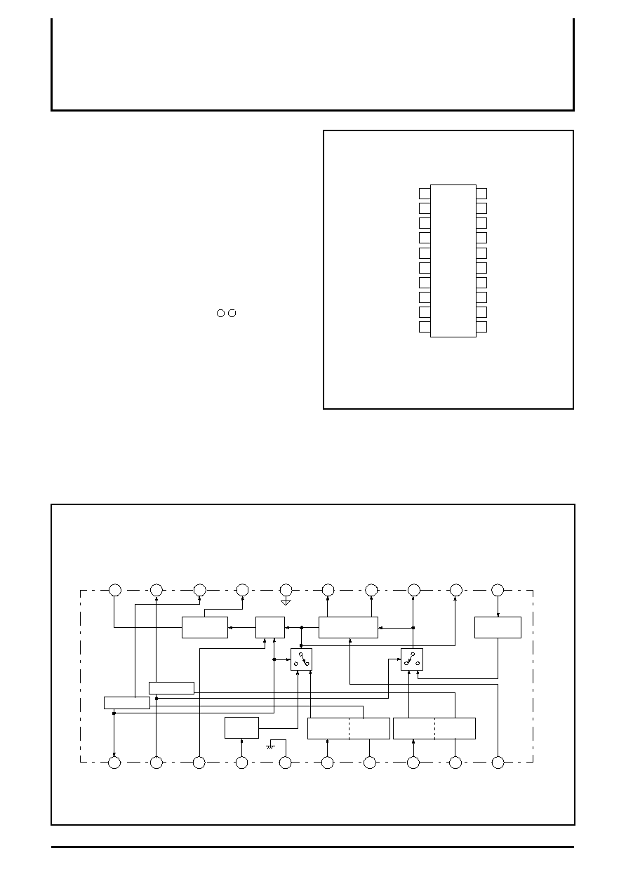
BLOCK DIAGRAM
PIN CONFIGURATION (TOP VIEW)
14
15
1
2
3
4
5
6
7
8
9
10
20
19
18
17
16
15
14
13
12
11
COMP/H
IN
H. STATE
COMP/H
DET
V. STATE
CLAMP
SW
GREEN
IN
V TIME GATA
SW
VD
+
OUT
V S/S
OUT
GND
V DET
V IN
H. POL.
CLAMP
+
OUT
V
CC
HD
-
OUT
HD
+
OUT
V S/S
IN
CLAMP
GET
EDGE
SW
CLAMP
TIMING
Y. POL.
H
DET
V. SYNC
SEP
V. TIME
GATE
LOGIC
H
SHAPE
V
SHAPE
V
DET
SYNC
SEP
LOGIC
Outline 20P4B(SP)
20
17
18
19
1
4
3
2
16
5
15
6
12
9
11
10
7
8
14
13
M52347SP/FP
CLAMP TIMING
Y. POL.
H. POL.
CLAMP
+
OUT
V
CC
HD
+
OUT
VD
+
OUT
V S/S OUT
V S/S IN
HD
-
OUT
COMP/H IN
H. STATE
COMP/H DET
V. STATE
CLAMP SW
GREEN IN
V TIME GATE SW
GND
V DET
V IN
20P2N-A(FP)

MITSUBISHI ICs (Monitor)
M52347SP/FP
SYNC SIGNAL PROCESSOR
2
ABSOLUTE MAXIMUM RATINGS
(Ta=25∞C, unless otherwise noted)
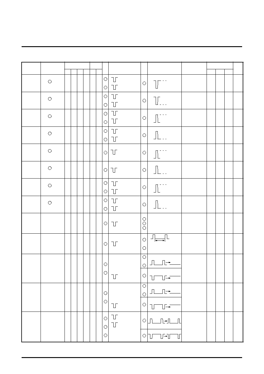
ELECTRICAL CHARACTERISTICS
(Ta=25∞C, Vcc=12V, unless otherwise noted)
Symbol
Parameter
Ratings
Unit
V
CC
Supply voltage
6.0
V
Pd
Power dissipation
1237.6(SP),827.8(FP)
mW
S
urge
Electrostatic discharge
±
200
V
T
opr
Operating temperature
-20 to +85
∞C
T
stg
Storage temperature
-40 to +150
∞C
Symbol
Parameter
Relay condition
TP
condition
In
put
pin
Input condition
Out
put
pin
Output waveform
Note
Limits
Unit
4
6
8
16
3
10
Min. Typ. Max.
Circuit
current
I
CC
2
2
2
2 5V 5V
A
40
53
66
mA
1 OH
Pin
output
Hi level
2
1
1
1
0V
2.5V
5V
5V
50kHz
1V
P-P
50kHz
1V
P-P
DC
4.0
5.0
5.0
V
1 OL
Pin
output
Low level
2
1
1
1
0V
2.5V
5V
5V
50kHz
0.2V
P-P
50kHz
1.0V
P-P
DC
0.2 V
P-P
of
input
signal is equiv-
alent to NON
SYNC.
0
0.04 0.5
V
2 OH
Pin
output
Hi level
2
1
1
1
0V
2.5V
5V
5V
50kHz
1V
P-P
50kHz
1V
P-P
DC
4.0
5.0
5.0
V
2 OL
Pin
output
Low level
2
1
1
1
0V
2.5V
5V
5V
50kHz
1.0V
P-P
50kHz
0.2V
P-P
DC
0.2 V
P-P
of
input
signal is equiv-
alent to NON
SYNC.
0
0.04 0.5
V
18 OH
Pin
output
Hi level
2
1
1
1
0V
2.5V
5V
5V
50kHz
1V
P-P
50kHz
1V
P-P
DC
4.0
5.0
5.0
V
18 OL
Pin
output
Low level
2
1
1
1
0V
2.5V
5V
5V
50kHz
1V
P-P
50kHz
1V
P-P
DC
0
0.04 0.5
V
19 OH
Pin
output
Hi level
2
1
1
1
0V
2.5V
5V
5V
50kHz
1V
P-P
50kHz
1V
P-P
DC
4.0
5.0
5.0
V
19 OL
Pin
output
Low level
2
1
1
1
0V
2.5V
5V
5V
50kHz
1V
P-P
50kHz
1V
P-P
DC
0
0.04 0.5
V
14 OH
Pin
output
Hi level
1
1
2
1
0V
2.5V
5V
5V
50kHz
0.6V
P-P
50kHz
2V
P-P
4.0
5.0
5.0
V
14 OL
Pin
output
Low level
1
1
2
1
0V
2.5V
5V
5V
50kHz
0.6V
P-P
50kHz
2V
P-P
0
0.25 0.5
V
16
1
6
8
1
1
6
8
1
2
6
8
2
2
6
8
2
18
6
8
18
18
6
8
18
19
6
8
19
19
6
8
19
14
4
6
14
V Meas
14
4
6
14
V Meas
The true value table depends on Table 1.
1
µ
S
1
µ
S
1
µ
S
1
µ
S
1
µ
S
1
µ
S
1
µ
S
1
µ
S
1
µ
S
1
µ
S
1
µ
S
1
µ
S
1
µ
S
1
µ
S
1
µ
S
1
µ
S
1
µ
S
1
µ
S
1
µ
S
1
µ
S
MITSUBISHI ICs (Monitor)
M52347SP/FP
SYNC SIGNAL PROCESSOR
3
ELECTRICAL CHARACTERISTICS
(cont.)
Symbol
Parameter
Relay condition
TP
condition
In
put
pin
Input condition
Out
put
pin
Output waveform
Note
Limits
Unit
4
6
8
16
3
10
Min. Typ. Max.
15 OH
Pin
output
Hi level
1
1
2
1
0V
2.5V
5V
5V
50kHz
0.6V
P-P
50kHz
2V
P-P
4.0
5.0
5.0
V
15 OL
Pin
output
Low level
1
1
2
1
0V
2.5V
5V
5V
50kHz
0.6V
P-P
50kHz
2V
P-P
0
0.25 0.5
V
17 OH
Pin
output
Hi level
1
1
2
1
0V
2.5V
5V
5V
50kHz
0.6V
P-P
50kHz
2V
P-P
4.0
5.0
5.0
V
17 OL
Pin
output
Hi level
1
1
2
1
0V
2.5V
5V
5V
50kHz
0.6V
P-P
50kHz
2V
P-P
0
0.25 0.5
V
13 OH
Pin
output
Hi level
2
2
1
1
0V
2.5V
5V
5V
50kHz
2V
P-P
4.0
5.0
5.0
V
13 OL
Pin
output
Low level
2
2
1
1
0V
2.5V
5V
5V
50kHz
2V
P-P
0
0.25 0.5
V
12 OH
Pin
output
Hi level
1
1
2
1
0V
2.5V
5V
5V
50kHz
0.6V
P-P
50kHz
2V
P-P
4.0
5.0
5.0
V
12 OL
Pin
output
Low level
1
1
2
1
0V
2.5V
5V
5V
50kHz
0.6V
P-P
50kHz
2V
P-P
0
0.25 0.5
V
SS-NV
Sync-Sep
Sync input
signa Max.
noise ampli-
tude voltage
1
2
2
1
0V
2.5V
5V
5V
50kHz
0.05V
P-P
No pulse must be
output.
Must not oper-
ate when input
amplitude is
0.05 V
P-P
or
less. (Pseudo
noise signal)
-
-
0.05 V
P-P
SS-LV
Sync-Sep
Sync input
signal
Min. ampli-
tude voltage
1
2
2
1
0V
2.5V
5V
5V
50kHz
0.2V
P-P
No pulse must be
output in this por-
tion.
Must operate
when the input
amplitude is
0.2 V
P-P
or
more.
0.2
-
-
V
P-P
V3H
CLAMP SW
Threshold
voltage H
2
1
2
1
5V
DC voltage must
be applied.
Checking output
pulse for output
with a voltage of
5 VDC applied,
decrease the DC
voltage and then
measure the volt-
age when the
output pulse is
not output.
2.8
3.1
3.4
V
50kHz
2V
P-P
V3L
CLAMP SW
Threshold
voltage H
Variable
2
1
2
1
5V
DC voltage must
be applied.
Checking output
pulse for output
with a voltage of
0 VDC applied,
increase the DC
voltage and then
measure the volt-
age when the
output pulse is
not output.
1.0
1.3
1.6
V
50kHz
2V
P-P
V10
V TIME
GATE SW
Threshold
voltageVari-
able
2
1
1
1
0V
5V
50kHz
2V
P-P
50kHz
2V
P-P
Checking output
pulse for output
with a voltage of
5 VDC applied,
decrease the DC
voltage and then
measure the volt-
age when the
output pulse
becomes narrow.
2.0
2.5
3.0
V
DC voltage must
be applied.
15
4
6
15
15
4
6
15
17
4
6
17
17
4
6
17
13
8
13
13
8
13
12
4
6
12
12
4
6
12
4
14
15
17
4
14
17
3
6
14
17
15
3
6
14
17
15
6
8
10
14
15
1
µ
S
1
µ
S
1
µ
S
1
µ
S
1
µ
S
1
µ
S
1
µ
S
1
µ
S
1
µ
S
1
µ
S
1
µ
S
1
µ
S
1
µ
S
1
µ
S
1
µ
S
1
µ
S
V Meas
V Meas
V Meas
V Meas
V Meas
V Meas
V Meas
V Meas
1
µ
S
1
µ
S
1
µ
S
1
µ
S
50kHz
V
a
r
iab
le
V
a
r
iab
le
V
a
r
iab
le
MITSUBISHI ICs (Monitor)
M52347SP/FP
SYNC SIGNAL PROCESSOR
4
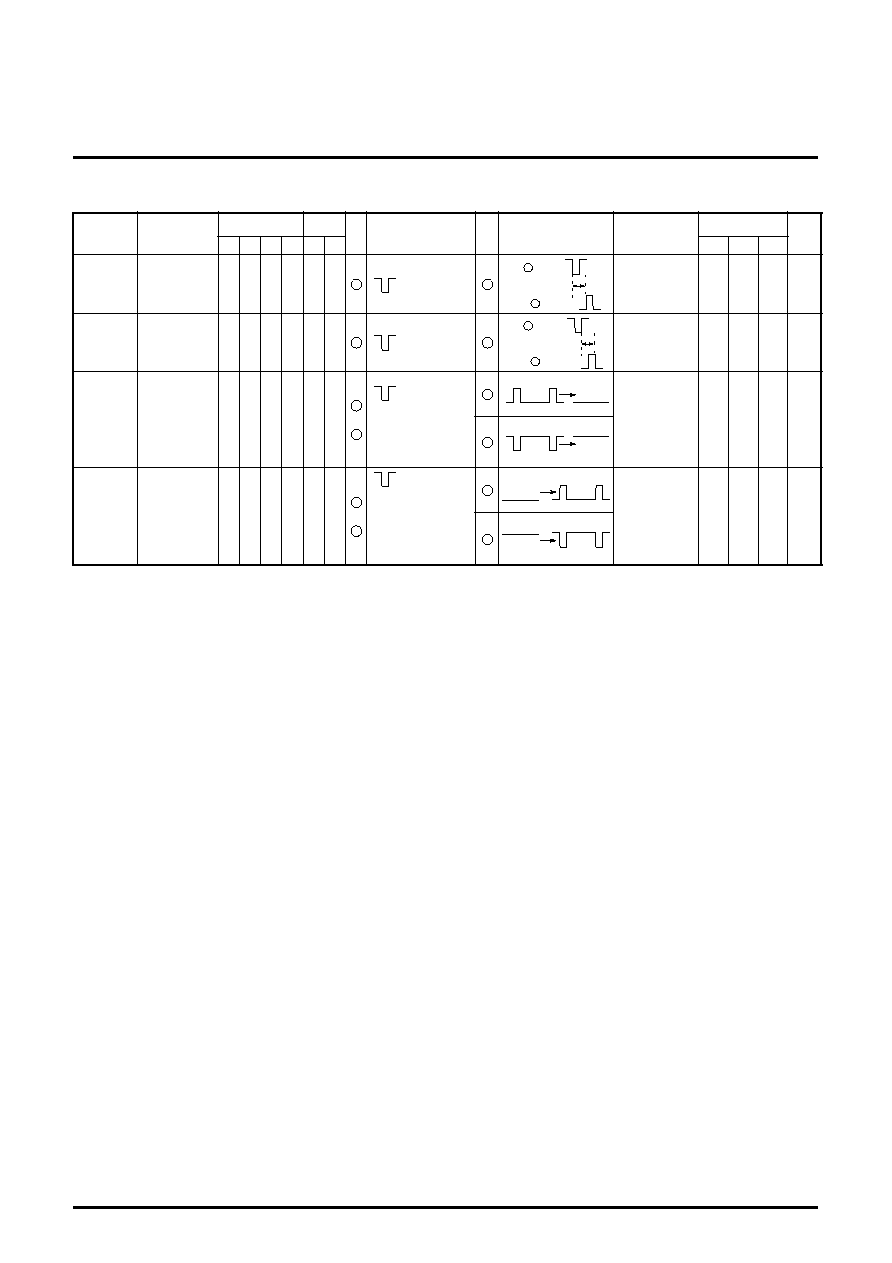
ELECTRICAL CHARACTERISTICS
(cont.)
Symbol
Parameter
Relay condition
TP
condition
In
put
pin
Input condition
Out
put
pin
Output waveform
Note
Limits
Unit
4
6
8
16
3
10
Min. Typ. Max.
HD
+
-DA
HD
+
-delay
time (A)
1
1
2
1
0V
5V
5V
50kHz
0.6V
P-P
50kHz
2V
P-P
Input
(50%)
Output
(50%)
-
120 350 nsec
HD
+
-DB
HD
+
-delay
time (B)
1
1
2
1
0V
5V
5V
50kHz
0.6V
P-P
50kHz
2V
P-P
Input
(50%)
Output
(50%)
-
80
350 nsec
HD
+
-DC
HD
+
-delay
time (C)
1
1
2
1
2.5V
5V
50kHz
0.6V
P-P
50kHz
2V
P-P
Input
(50%)
Output
(50%)
-
140 350 nsec
HD
+
-DD
HD
+
-delay
time (D)
1
1
2
1
2.5V
5V
50kHz
0.6V
P-P
50kHz
2V
P-P
nput
(50%)
Output
(50%)
-
120 350 nsec
HD
-
-DA
HD
-
-delay
time (A)
1
1
2
1
0V
5V
5V
50kHz
0.6V
P-P
50kHz
2V
P-P
nput
(50%)
Output
(50%)
-
70
350 nsec
HD
-
-DB
HD
-
-delay
time (B)
1
1
2
1
0V
5V
5V
50kHz
0.6V
P-P
50kHz
2V
P-P
nput
(50%)
Output
(50%)
-
120 350 nsec
HD
-
-DC
HD
-
-delay
time (C)
1
1
2
1
2.5V
5V
50kHz
0.6V
P-P
50kHz
2V
P-P
Input
(50%)
Output
(50%)
-
100 350 nsec
HD
-
-DD
HD
-
-delay
time (D)
1
1
2
1
2.5V
5V
50kHz
0.6V
P-P
50kHz
2V
P-P
Input
(50%)
Output
(50%)
-
150 350 nsec
CP
+
-DA
CP
+
-delay
time (A)
1
1
2
1
0V
5V
50kHz
0.6V
P-P
50kHz
2V
P-P
nput
(50%)
Output
(50%)
-
90
350 nsec
CP
+
-DB
CP
+
-delay
time (B)
1
1
2
1
2.5V
5V
50kHz
0.6V
P-P
50kHz
2V
P-P
nput
(50%)
Output
(50%)
-
130 350 nsec
CP
+
-DC
CP
+
-delay
time (C)
1
1
2
1
5V
5V
50kHz
0.6V
P-P
50kHz
2V
P-P
nput
(50%)
Output
(50%)
-
90
350 nsec
CP
+
-PW
CP
+
-PULSE
-WIDTH
1
1
2
1
0V
2.5V
5V
5V
50kHz
0.6V
P-P
50kHz
2V
P-P
Output
(50%)
250 400 550 nsec
4
6
14
6
14
4
6
14
6
14
4
6
14
4
14
4
6
14
4
14
4
6
15
6
15
4
6
15
6
15
4
6
15
4
15
4
6
15
4
15
4
6
17
6
17
4
6
17
4
17
4
6
17
6
17
4
6
17
17
Time
Meas
1
µ
S
1
µ
S
1
µ
S
1
µ
S
1
µ
S
1
µ
S
1
µ
S
1
µ
S
1
µ
S
1
µ
S
1
µ
S
1
µ
S
1
µ
S
1
µ
S
1
µ
S
1
µ
S
1
µ
S
1
µ
S
1
µ
S
1
µ
S
1
µ
S
1
µ
S
1
µ
S
1
µ
S
Time
Meas
Time
Meas
Time
Meas
Time
Meas
Time
Meas
Time
Meas
Time
Meas
Time
Meas
Time
Meas
Time
Meas
Time
Meas
MITSUBISHI ICs (Monitor)
M52347SP/FP
SYNC SIGNAL PROCESSOR
5
ELECTRICAL CHARACTERISTICS
(cont.)
Symbol
Parameter
Relay condition
TP
condition
In
put
pin
Input condition
Out
put
pin
Output waveform
Note
Limits
Unit
4
6
8
16
3
10
Min. Typ. Max.
VD
+
-DA
VD
+
-delay
time (A)
2
2
1
1
0V
2.5V
5V
5V
50kHz
2V
P-P
Input
(50%)
Output
(50%)
-
100 350 nsec
VD
+
-DB
VD
+
-delay
time (B)
2
2
1
1
0V
2.5V
5V
5V
50kHz
2V
P-P
Input
(50%)
Output
(50%)
-
70
350 nsec
V11H
V Sync-Sep
Threshold
voltage H
2
1
2
1
0V
5V
0V
50kHz
2V
P-P
Checking output
pulse for output
with a voltage of
0 VDC applied,
increase the DC
voltage and then
measure the volt-
age when the
output pulse is
not output.
3.0
3.5
4.0
V
DC voltage must
be applied.
V11L
V Sync-Sep
Threshold
voltage L
2
1
2
1
0V
5V
0V
50kHz
2V
P-P
Checking output
pulse for output
with a voltage of
5 VDC applied,
decrease the DC
voltage and then
measure the volt-
age when the
output pulse is
output.
1.3
1.8
2.3
V
DC voltage must
be applied.
8
13
8
13
8
13
8
13
6
11
14
15
6
11
14
15
1
µ
S
1
µ
S
1
µ
S
1
µ
S
Time
Meas
Time
Meas