 | ÐлекÑÑоннÑй компоненÑ: M54640P | СкаÑаÑÑ:  PDF PDF  ZIP ZIP |
Äîêóìåíòàöèÿ è îïèñàíèÿ www.docs.chipfind.ru
STEPPER MOTOR DRIVER
M54640P
MITSUBISHI <CONTROL / DRIVER IC>
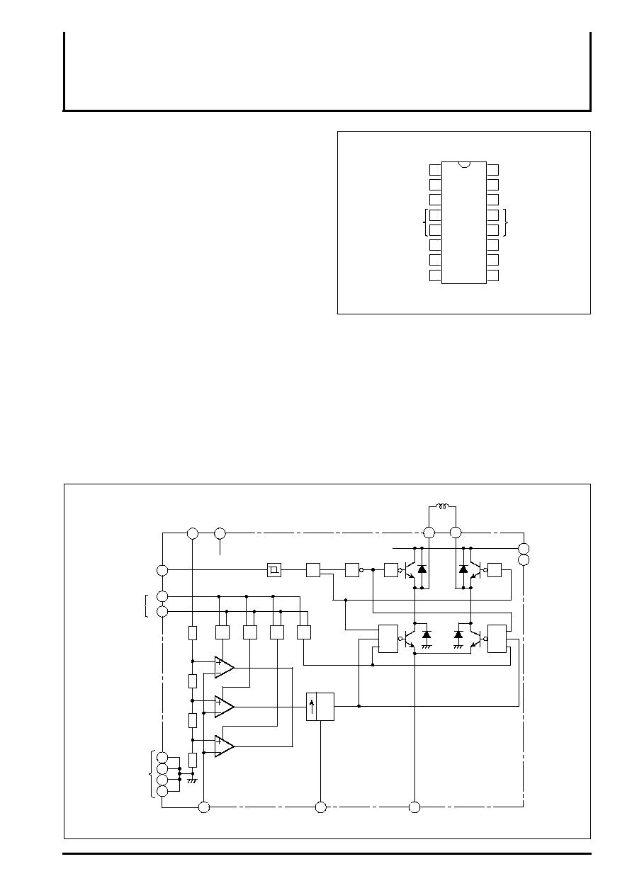
PIN CONFIGURATION (TOP VIEW)
each comparator, and then each comparator output triggers
monomulti and the current is cut for a certain time (t
OFF
) by utilizing
the inductance of the coil.
Also, diodes needed for choppering and a thermal shutdown circuit
as a countermeasure against overvoltage are built in this circuit.
BLOCK DIAGRAM
DESCRIPTION
The M54640P is a semiconductor IC to drive a stepper motor by
the bipolar method.
FEATURES
q
Bipolar and constant-current drive
q
Wide current control rage (20 800mA)
q
Wide supply voltage drive range (10 40V)
q
Built in flywheel diodes
q
Current level can be changed by steps or continuously.
q
Built in a thermal shutdown circuit
APPLICATION
Printer, FDD, HDD, Fax
FUNCTION
The M54640P drives a stepper motor by the bipolar drive method to
change the current direction of a single coil and controls the current
direction with PHASE input pin. In order to obtain higher efficiency,
the constant current drive system to control the coil current is
introduced. The current value can be selected among four levels (0
to max.) by selecting the combination of three internal comparators
by logic input. It also can be continuously changed by controlling
the reference voltage. Conversion to voltage is conducted by the
current value sensing resistor (R
s
) and the voltage is sensed with
Schmitt trigger
11
V
R
V
CC
6
8
7
9
4
5
12
13
10
2
16
15
1
3
14
1
>
1
1
>
1
00
01
10
11
M
A
M
B
V
MM
P
h
I
1
I
0
V
KH
V
KM
V
KL
Comparator reference input
Comparator input
C
T
E
One-shot-multi time constant
Current sensor
Current sensor
Output
Output
Cutput current
direction switcing
Output current
value setting
GND
Monostable
t
OFF
= 0.69 · R
T
C
T
1
Output power
supply
16
13
14
15
1
4
3
2
12
5
11
6
10
7
9
8
Outline 16P4
Output
One-shot-multi
time constant
Output power
Power supply
Output current
Output current
Current sensor
Output
Output power
Comparator
reference input
Comparator input
Output current
M
B
T
V
MM
GND
V
CC
I
1
P
h
E
M
A
V
MM
V
R
C
Io
GND
M5
4640P
setting
direction switching
value setting
supply
supply
STEPPER MOTOR DRIVER
M54640P
MITSUBISHI <CONTROL / DRIVER IC>
RECOMMENDED OPERATING CONDITIONS (Ta=25
°
C, unless otherwise noted)
ABSOLUTE MAXIMUM RATINGS (Ta=25
°
C, unless otherwise noted)
Symbol
Ratings
Unit
Parameter
Conditions
V
CC
V
MM
V
L
V
C
V
R
I
L
I
C
I
MM
P
d
T
opr
T
stg
Supply voltage
Output supply voltage
Analog input voltage
Comparative input voltage
Logic input current
Analog input current
Output supply current
Power dissipation
Operating temperature
Storage temperature
Logic input voltage
Mounted on a board
-0.3 7
-0.3 45
-0.3 6
-0.3 V
CC
-0.3 15
-10
-10
±
1000
1.92
-20 75
-55 125
V
V
V
V
V
mA
mA
mA
W
°
C
°
C
Note. Every voltage value is measured when the voltage at GND pin is 0V. The maximum and the minimum of each voltage value are shown in absolute values.
Regarding current directions, inflow current is shown in a positive value and outflow current is shown in a negative value. The maximum and the minimum
of each current value are shown in absolute values.
Symbol
Parameter
Limits
Min.
Typ.
Max.
Unit
V
CC
V
MM
I
O
t
PLH
t
PHL
T
ON
Supply voltage
Output supply voltage
Output current
Logic input rise time
Logic input fall time
Thermal shutdown temperature
4.75
10
20
5
175
5.25
40
800
2
2
V
V
mA
µ
s
µ
s
°
C
ELECTRICAL CHARACTERISTICS (V
CC
=5V, Ta=25
°
C, unless otherwise noted)
Limits
Min.
Typ.
Max.
Symbol
Test conditions
Unit
Parameter
V
IH
V
IL
V
CH
V
CM
V
CL
I
CO
I
OFF
V
sat
t
OFF
t
d
I
CC
I
IH
I
IL
Logic input voltage
Comparator threshold
Comparator input current
Output cutoff current
Saturation voltage
Cutoff time
Turnoff delay
Supply current
Logic input current
The voltage at the sensing resistor is not
included. I
O
=500mA
"H"
"L"
"H"
"L"
V
CC
=5V
V
R
=5V, I
0
=I
1
=0
V
R
=5V, I
0
=1,I
1
=0
V
R
=5V, I
0
=0, I
1
=1
I
0
=I
1
=1(Ta=25
°
C)
V
MM
=10V, t
ON
5
µ
s
Ta=25
°
C, dVK/dt
50mV/
µ
s
V
CC
=5V
V
I
=2.4V
V
I
=0.4V
2.0
0
400
240
75
-20
25
430
260
90
30
1.6
V
CC
0.8
450
280
100
20
100
4.0
35
2.0
25
20
-0.4
V
mV
µ
A
µ
A
V
µ
s
µ
s
mA
µ
A
mA
STEPPER MOTOR DRIVER
M54640P
MITSUBISHI <CONTROL / DRIVER IC>
SWITCHING CHARACTERISTICS
I
0
H
L
H
L
I
1
H
Current level
H
L
L
0
Low
Average
High
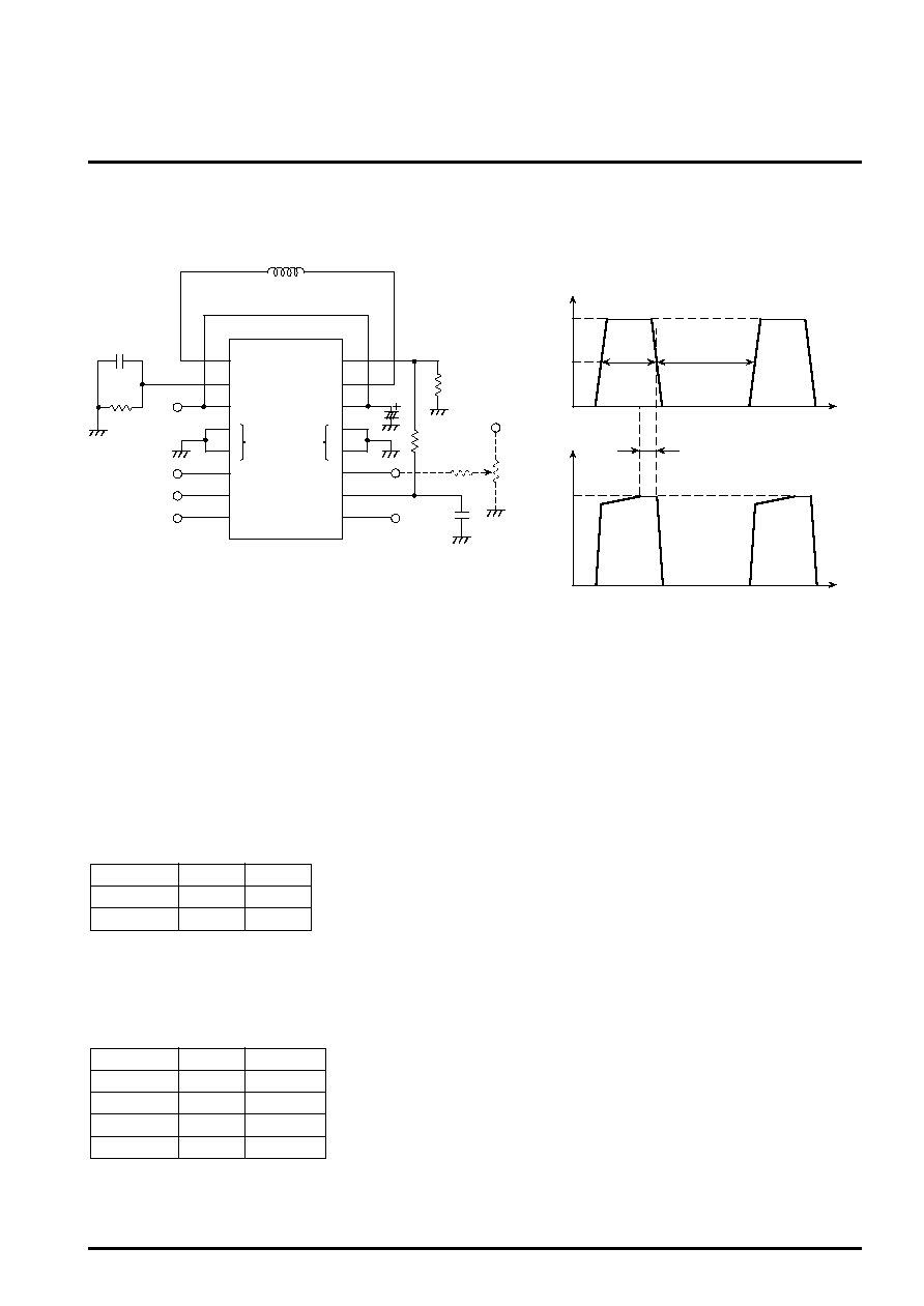
APPLICATION DESCRIPTION
Test circuit
Switching waveforms
· PHASE INPUT
Phase input decides the output mode.
· Current sensor
When the voltage fall at the current sensing resistor and the
selected current level becomes of the same level, the comparator
triggers the monostable. Then, the output stage is cut off for a
certain time (t
OFF
). During this cutoff time, the current volume
decreases slightly and falls short of the comparison level.
After the cutoff time (t
OFF
), the output stage is in ON state again.
This operation is repeated.
· Single pulse generator
At the comparator output rise edge, the monostable is triggered.
The pulse width of the monostable at the external timing R
t
and
C
t
is as follows.
t
OFF
= 0.69 x R
t
C
t
Retrigger during t
OFF
is neglected.
· Analog control
The output current level can be continuously changed by
changing the voltage at V
R
or the feedback voltage to the
comparator.
· I
0
, I
1
I
0
and I
1
fixed based on the comparison voltage V
R
decide the
output current level.
The current level can be continuously changed by changing the
voltage at V
R
continuously.
PHASE
H
L
M
A
H
M
B
L
L
H
8
7
1
2
3
4
5
6
M
B
T
V
MM
GND
V
CC
I
1
Phase
E
M
A
V
MM
V
R
I
0
C 10
9
R
S
R
C
C
V
C
C
V
CC
C
T
R
T
GND
11
12
13
14
15
16
:
1
: 1k
: 56k
: 820pF
: 820pF
: 47
µ
F
R
S
R
C
R
T
C
C
C
T
C
V
1
1/2
t
ON
t
OFF
t
OFF
= 0.69RTCT
V
MA
V
MB
or V
MB
V
MA
t
d
V
CH
V
CM
V
CL
STEPPER MOTOR DRIVER
M54640P
MITSUBISHI <CONTROL / DRIVER IC>
TIMING CHART
Phase A
Phase B
I
0
,
1
= (A) = 0
I
0
,
1
= (B) = 0
Phase A
Phase B
I
0, 1
= (B)
Phase A
Phase B
I
0
(B)
I
1
(B)
I
0
(A)
I
1
(A)
2-phase excitation
1-2-phase excitation
Microstep (divided into six)
I
0, 1
= (A)
STEPPER MOTOR DRIVER
M54640P
MITSUBISHI <CONTROL / DRIVER IC>
TYPICAL CHARACTERISTICS (Absolute maximum ratings)
Safety operating temperature
Output current Io
(A)
1.0
0.8
0.6
0.4
0.2
0
0
10
20
30
40 45
50
A
B
C
Output V
MM
(V)
Recommended
Schottky diodes should be externally connected between
output pins and power supply pins.
Schottky diodes should be externally instaalled between
output pins and power supply pins and between output
pins and GND pin.
A :
B :
C :
Mounted on a 25cm
2
glass epoxy board which is coated
with copper on one side.
c-a
= 45
°
C/W
10cm
2
aluminum heat sink (1t) is used.
c-a
= 25
°
C/W
100cm
2
aluminum heat sink (1t) is used.
c-a
= 10
°
C/W
T
j(max)
= 150
°
C
A :
j-c
= 10
°
C/W
B :
C :
Ambient (
°
C)
10.0
8.0
6.0
4.0
2.0
0
0
25
75
50
A
B
C
Allowable power
dissipation
(W)
100
Thermal derating