MITSUBISHI ELECTRIC
M5M5V216ATP,RT
revision-01, ' 98.12.08
2097152-BIT (131072-WORD BY 16-BIT) CMOS STATIC RAM
MITSUBISHI LSIs
PIN CONFIGURATION
DESCRIPTION
Single +2.7~+3.6V power supply
Small stand-by current: 0.3µA(3V,typ.)
No clocks, No refresh
Data retention supply voltage=2.0V to 3.6V
All inputs and outputs are TTL compatible.
Easy memory expansion by S , BC1 and BC2
Common Data I/O
Three-state outputs: OR-tie capability
OE prevents data contention in the I/O bus
Process technology: 0.25µm CMOS
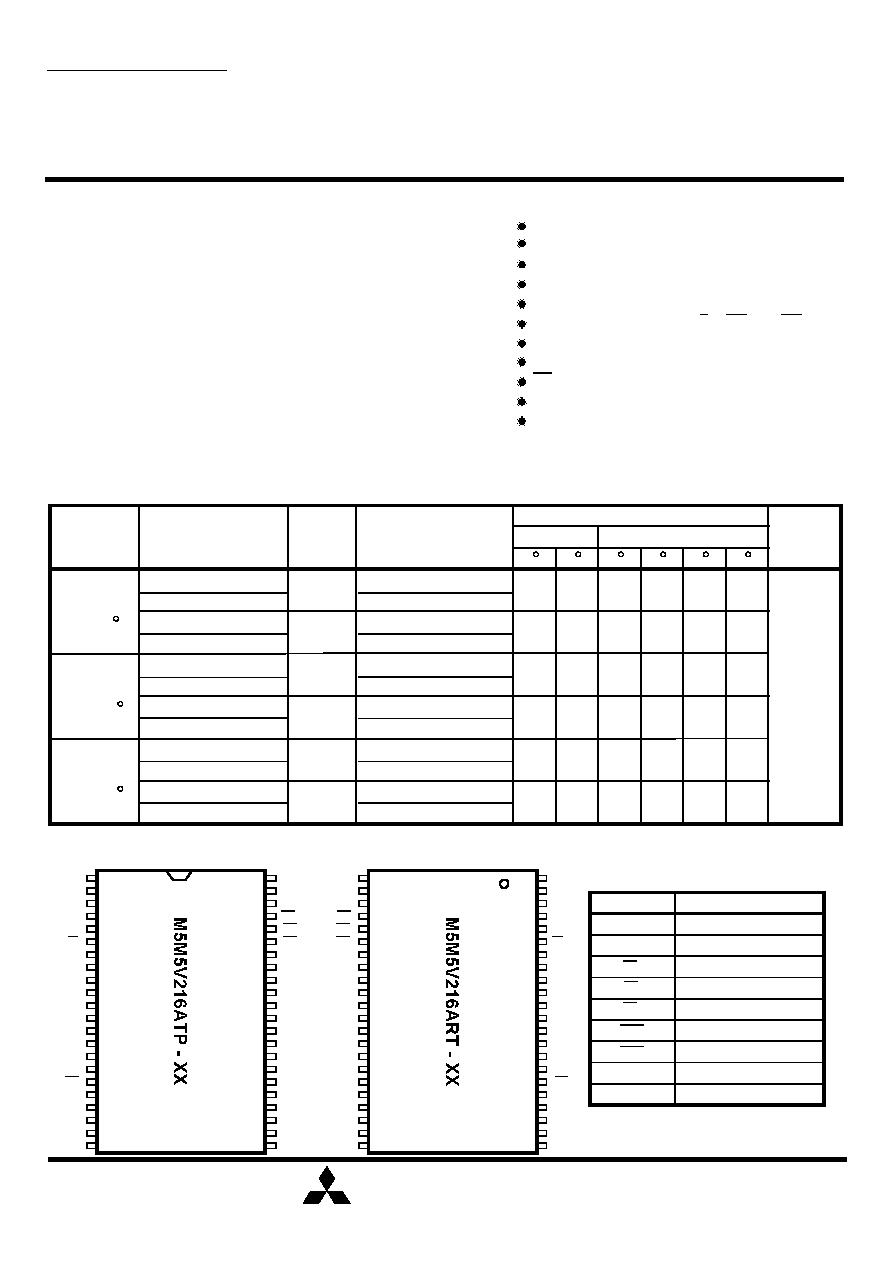
Package: 44 pin 400mil TSOP (II)
FEATURES
1
The M5M5V216A is a family of low voltage 2-Mbit static RAMs
organized as 131,072-words by 16-bit, fabricated by Mitsubishi's
high-performance 0.25µm CMOS technology.
The M5M5V216A is suitable for memory applications where a
simple interfacing , battery operating and battery backup are the
important design objectives.
M5M5V216ATP, RT are packaged in a 44-pin 400mil thin small
outline package. M5M5V216ATP (normal lead bend type package)
, M5M5V216ART (reverse lead bend type package) , both types
are very easy to design a printed circuit board.
From the point of operating temperature, the family is divided into
three versions; "Standard", "W-version", and "I-version". Those are
summarized in the part name table below.
PART NAME TABLE
Standard
0 ~ +70 C
W-
version
-20 ~ +85 C
I-
version
-40 ~ +85 C
Version,
Part name
Power
Supply
Access
time
max.
25 C
Stand-by current Icc
(PD)
, Vcc=3.0V
55ns(@ 2.7V) / 50ns(@3.3V)
2.7 ~ 3.6V
2.7 ~ 3.6V
2.7 ~ 3.6V
2.7 ~ 3.6V
2.7 ~ 3.6V
2.7 ~ 3.6V
---
---
---
0.3µA
0.3µA
0.3µA
---
1µA
1µA
3µA
1µA
3µA
typical *
---
---
---
40 C
1µA
1µA
1µA
---
---
20µA
8µA
20µA
8µA
50µA
24µA
20µA
8µA
50µA
24µA
70 C
85 C
25 C
40 C
---
---
---
---
---
3µA
Active
current
45mA
(10MHz)
5mA
(1MHz)
Ratings (max.)
Operating
temperature
(3.0V, typ.)
Icc1
* "typical" parameter is sampled, not 100% tested.
Outline: TP :
44P3W - H
RT : 44P3W - J
NC: No Connection
A0 ~ A16
DQ1 ~ DQ16
S
W
OE
BC1
Address input
Data input / output
Chip select input
Write control input
Output inable input
Lower Byte (DQ1 ~ 8)
Pin
Function
Vcc
GND
Power supply
Ground supply
BC2
Upper Byte (DQ9 ~ 16)
BC1
OE
A4
A3
BC2
S
A5
DQ1
NC
Vcc
GND
W E
NC
A8
A9
A10
A11
1
2
3
4
5
6
7
8
9
10
11
12
13
14
15
16
17
18
19
20
21
22
44
43
42
41
40
39
38
37
36
35
34
33
32
31
30
29
28
27
26
25
24
23
A2
A1
A0
DQ2
DQ3
DQ4
DQ5
DQ6
DQ7
DQ8
A16
A15
A14
A13
A12
DQ9
DQ10
DQ11
DQ12
Vcc
GND
DQ13
DQ14
DQ15
DQ16
A6
A7
1
2
3
4
5
6
7
8
9
10
11
12
13
14
15
16
17
18
19
20
21
22
44
43
42
41
40
39
38
37
36
35
34
33
32
31
30
29
28
27
26
25
24
23
A4
A3
S
DQ1
Vcc
GND
W E
A2
A1
A0
DQ2
DQ3
DQ4
DQ5
DQ6
DQ7
DQ8
A16
A15
A14
A13
A12
BC1
OE
BC2
A5
NC
NC
A8
A9
A10
A11
DQ9
DQ10
DQ11
DQ12
Vcc
GND
DQ13
DQ14
DQ15
DQ16
A6
A7
M5M5V216ATP , RT -70L
70ns(@ 2.7V) / 65ns(@3.3V)
M5M5V216ATP , RT -55H
55ns(@ 2.7V) / 50ns(@3.3V)
M5M5V216ATP , RT -70H
70ns(@ 2.7V) / 65ns(@3.3V)
M5M5V216ATP , RT -55LW
55ns(@ 2.7V) / 50ns(@3.3V)
M5M5V216ATP , RT -70LW
70ns(@ 2.7V) / 65ns(@3.3V)
M5M5V216ATP , RT -55HW
55ns(@ 2.7V) / 50ns(@3.3V)
M5M5V216ATP , RT -70HW
70ns(@ 2.7V) / 65ns(@3.3V)
M5M5V216ATP , RT -55L I
55ns(@ 2.7V) / 50ns(@3.3V)
M5M5V216ATP , RT -70L I
70ns(@ 2.7V) / 65ns(@3.3V)
M5M5V216ATP , RT -55H I
55ns(@ 2.7V) / 50ns(@3.3V)
M5M5V216ATP , RT -70H I
70ns(@ 2.7V) / 65ns(@3.3V)
M5M5V216ATP , RT -55L
MITSUBISHI ELECTRIC
M5M5V216ATP,RT
revision-01, ' 98.12.08
2097152-BIT (131072-WORD BY 16-BIT) CMOS STATIC RAM
MITSUBISHI LSIs
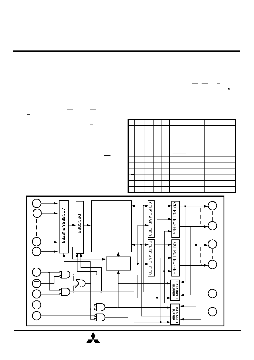
FUNCTION TABLE
2
FUNCTION
The M5M5V216ATP,RT is organized as 131,072-words by
16-bit. These devices operate on a single +2.7~3.6V power
supply, and are directly TTL compatible to both input and
output. Its fully static circuit needs no clocks and no
refresh, and makes it useful.
The operation mode are determined by a combination of
the device control inputs BC1 , BC2 , S , W and OE.
Each mode is summarized in the function table.
A write operation is executed whenever the low level W
overlaps with the low level BC1 and/or BC2 and the low
level S. The address(A0~A16) must be set up before the
write cycle and must be stable during the entire cycle.
A read operation is executed by setting W at a high level
and OE at a low level while BC1 and/or BC2 and S are in
an active state(S=L).
When setting BC1 at the high level and other pins are in
an active stage , upper-byte are in a selesctable mode in
which both reading and writing are enabled, and lower-byte
are in a non-selectable mode. And when setting BC2 at a
high level and other pins are in an active stage, lower-
byte are in a selectable mode and upper-byte are in a
non-selectable mode.
When setting BC1 and BC2 at a high level or S at a high
level, the chips are in a non-selectable mode in which both
reading and writing are disabled. In this mode, the output
stage is in a high-impedance state, allowing OR-tie with
other chips and memory expansion by BC1, BC2 and S.
The power supply current is reduced as low as 0.3µA(25 C,
typical), and the memory data can be held at +2V power
supply, enabling battery back-up operation during power
failure or power-down operation in the non-selected mode.
BLOCK DIAGRAM
Mode
S
W
H
X
X
High-Z
S BC1 BC2
OE
DQ1~8
X
X
Non selection
DQ9~16
Icc
High-Z Standby
High-Z High-Z
L
X
L
L
H
Din
High-Z
Active
L
H
L
H
Read
High-Z
Dout
Active
L
L
H
L
Active
L
H
L
Active
L
L
High-Z
High-Z
Active
H
L
H
H
High-Z
L
L
Dout
H
L
L
Read
Dout
Active
L
L
Din
L
L
X
Write
Din
Active
H
High-Z
H
H
High-Z High-Z
Non selection
H
H
X
X
Standby
Write
L
H
L
L
Write
Din
Active
X
L
L
H
Read
High-Z
Active
L
Dout
H
High-Z
MEMORY ARRAY
131072 WORDS
x 16 BITS
CLOCK
GENERATOR
A
0
A
1
A
15
A
16
S
BC1
BC2
W
OE
DQ
8
DQ
1
DQ
16
DQ
9
-
Vcc
GND
L
MITSUBISHI ELECTRIC
M5M5V216ATP,RT
revision-01, ' 98.12.08
2097152-BIT (131072-WORD BY 16-BIT) CMOS STATIC RAM
MITSUBISHI LSIs
3
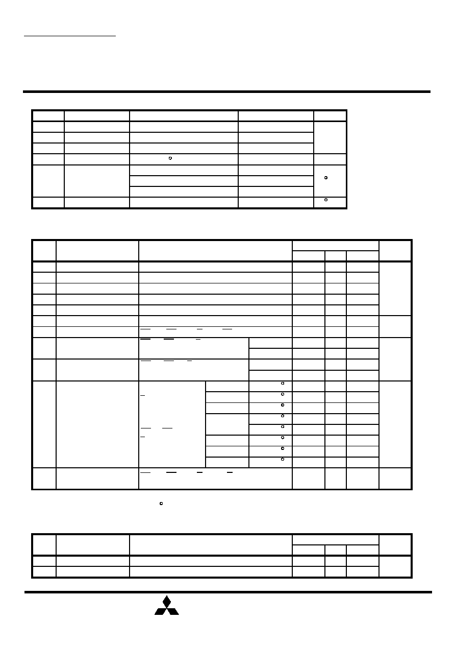
ABSOLUTE MAXIMUM RATINGS
pF
8
10
V
I
=GND, V
I
=25mVrms, f=1MHz
V
O
=
GND,V
O
=25mVrms, f=1MHz
C
I
C
O
Symbol
Parameter
Limits
Conditions
Units
µA
mA
µA
mA
V
Icc
1
Icc
2
Icc
4
V
IH
V
IL
I
O
Icc
3
V
OH1
I
OH
= -0.5mA
V
OH2
I
OH
= -0.05mA
V
OL
I
OL
=2mA
I
I
V
I
=0
~
Vcc
BC1 and BC2=V
IH
or S=V
IH
or OE=V
IH
, V
I/O
=0 ~ Vcc
Vcc+0.3V
0.6
2.0
-0.3 *
2.4
0.5
0.4
±1
60
45
10
Vcc-0.5V
±1
15
-HW, -HI
Max
Typ
Min
DC ELECTRICAL CHARACTERISTICS
+70 C
+40 ~ +70 C
+25 ~ +40 C
0.3
f= 10MHz
f= 1MHz
-
-
-
-
-
-
-
-
-
-
Supply voltage
Input voltage
Output voltage
Power dissipation
Operating
temperature
Storage temperature
V
mW
C
C
Conditions
Ta=25 C
700
- 20 ~ +85
- 65 ~ +150
Ratings
Vcc
V
I
V
O
P
d
T
a
T
stg
-0.5
*
~ +4.6
-0.5
*
~ Vcc + 0.5
0 ~ Vcc
Symbol
Parameter
Units
- 40 ~ +85
0 ~ +70
Standard
W-version
I-version
With respect to GND
f= 10MHz
f= 1MHz
5
60
45
15
5
+70 ~ +85 C
+70 ~ +85 C
-L, -LW, -LI
- 20 ~ +25 C
- 40 ~ +25 C
-H, -HW, -HI
0 ~ +25 C
-H
-HW
-HI
-
-LW, -LI
-
-
0.3
0.3
1
2
5
-
-
-
-
30
25
60
-
(-L, -H)
(-LW, -HW)
(-LI, -HI)
With respect to GND
With respect to GND
( Vcc=2.7 ~ 3.6V, unless otherwise noted)
High-level input voltage
Low-level input voltage
High-level output voltage 1
High-level output voltage 2
Low-level output voltage
Input leakage current
Output leakage current
Active supply current
( AC,MOS level )
( AC,TTL level )
Active supply current
Stand by supply current
( AC,MOS level )
( AC,TTL level )
Stand by supply current
Other inputs= 0 ~ Vcc
* -3.0V in case of AC (Pulse width 30ns)
Note 1: Direction for current flowing into IC is indicated as positive (no mark)
Note 2: Typical value is for Vcc=3.0V and Ta=25 C
CAPACITANCE
(Vcc=2.7 ~ 3.6V, unless otherwise noted)
Symbol
Parameter
Conditions
Limits
Max
Typ
Min
Units
Input capacitance
Output capacitance
* -3.0V in case of AC (Pulse width 30ns)
BC1 and BC2 0.2V , S 0.2V
other inputs 0.2V or Vcc-0.2V
Output - open (duty 100%)
<
=
<
=
>
=
BC1 and BC2=V
IL
, S=V
IL
<
=
other pins =V
IH or
V
IL
Output - open (duty 100%)
BC1 and BC2 Vcc - 0.2V
Other inputs=0~Vcc
S Vcc - 0.2V,
other inputs = 0 ~ Vcc
>
=
>
=
S 0.2V
<
=
< 1 >
< 2 >
BC1 and BC2=V
IH ,
S=V
IL
or S=V
IH
2
2
<
=
<
=

MITSUBISHI ELECTRIC
M5M5V216ATP,RT
revision-01, ' 98.12.08
2097152-BIT (131072-WORD BY 16-BIT) CMOS STATIC RAM
MITSUBISHI LSIs
4
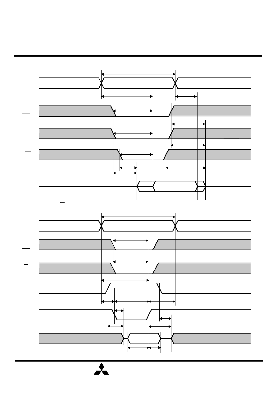
AC ELECTRICAL CHARACTERISTICS
(Vcc=2.7 ~ 3.6V, unless otherwise noted)
1TTL
CL
DQ
Input rise time and fall time
Reference level
Output loads
2.7V~3.6V
V
IH
=2.2V,V
IL
=0.4V
V
OH
=V
OL
=1.5V
Transition is measured ±500mV from
steady state voltage.(for t
en
,t
dis
)
5ns
Fig.1,CL=30pF
CL=5pF (for ten,tdis)
(1) TEST CONDITIONS
Supply voltage
Input pulse
Fig.1 Output load
Including scope and
jig capacitance
Output disable time after S high
t
CR
ns
t
a
(S)
t
a
(OE)
t
dis
(S)
t
dis
(OE)
t
en
(S)
t
en
(OE)
t
V
(A)
t
a
(A)
70
10
35
ns
ns
ns
ns
ns
ns
ns
ns
(2) READ CYCLE
Symbol
Parameter
Limits
Units
Max
Min
Read cycle time
Address access time
Chip select access time
Output enable access time
Data valid time after address
t
a
(BC1)
t
a
(BC2)
Byte control 1 access time
Byte control 2 access time
t
dis
(BC1)
t
dis
(BC2)
Output disable time after BC1 high
Output disable time after BC2 high
Output disable time after OE high
t
en
(BC1)
t
en
(BC2)
Output enable time after BC1 low
Output enable time after BC2 low
Output enable time after S low
Output enable time after OE low
ns
ns
ns
ns
ns
ns
70
70
70
70
25
25
25
25
10
10
5
10
(3) WRITE CYCLE
t
su
(A-WH)
t
CW
t
w
(W)
t
su
(A)
t
su
(S)
t
su
(D)
t
h
(D)
t
rec
(W)
t
dis
(W)
t
dis
(OE)
t
en
(W)
t
en
(OE)
Chip select setup time
ns
70
ns
ns
ns
ns
ns
ns
ns
ns
Symbol
Parameter
Limits
Units
Max
Min
Write cycle time
Write pulse width
Address setup time
Address setup time with respect to W
Byte control 1 setup time
Data setup time
Data hold time
Write recovery time
Output disable time from OE high
Output enable time from W high
Output disable time from W low
Output enable time from OE low
ns
ns
ns
ns
ns
55
0
65
25
25
5
5
t
su
(BC1)
t
su
(BC2)
Byte control 2 setup time
65
65
65
30
0
0
55
10
30
Max
Min
55
55
55
55
20
20
20
20
10
10
5
10
M5M5V216ATP,RT - 70
M5M5V216ATP,RT - 55
55
Max
Min
45
0
50
20
20
5
5
50
50
50
25
0
0
M5M5V216ATP,RT - 70
M5M5V216ATP,RT - 55
MITSUBISHI ELECTRIC
M5M5V216ATP,RT
revision-01, ' 98.12.08
2097152-BIT (131072-WORD BY 16-BIT) CMOS STATIC RAM
MITSUBISHI LSIs
t
en
(W)
5
t
a
(A)
t
a
(BC1)
t
v
(A)
t
dis
(BC1) or
t
dis
(BC1)
t
a
(OE)
t
en
(OE)
t
dis
(OE)
t
CR
t
h
(D)
t
su
(D)
DQ
1~16
t
su
(BC1) or
t
su
(BC2)
t
en
(OE)
t
dis
(OE)
t
w
(W)
t
rec
(W)
t
su
(A)
t
dis
(W)
t
CW
t
en
(S)
W = "H" level
A
0~16
DQ
1~16
A
0~16
OE
OE
W
(4)TIMING DIAGRAMS
Read cycle
(Note3)
(Note3)
(Note3)
(Note3)
VALID DATA
Write cycle ( W control mode )
DATA IN
STABLE
(Note3)
(Note3)
t
a
(S)
t
dis
(S)
S
(Note3)
(Note3)
BC1
BC2
and / or
t
a
(BC2)
or
t
en
(BC2)
t
en
(BC1)
t
su
(A-WH)
S
(Note3)
(Note3)
BC1
BC2
and / or
t
su
(S)