
M63016FP
Spindle Motor AND 4CH ACTUATOR Drive IC
MITSUBISHI SEMICONDUCTORS
MITSUBISHI ELECTRIC CORPORATION REV.011126
20
[FEATURES]
[APPLICATION]
CD-ROM, DVD, DVD-ROM, DVD-RAM,Optical disc related system,etc
This IC is 1 chip driver IC for Spindle Motor and 4 channel
actuators. All of the Motor and actuator of optical disk drive
system (CD-ROM etc.) can be driven by only this IC.
This IC has current control drive system for Focus,
Tracking, Spindle and Slide channel drive, also has a direct
PWM control system for Spindle and Slide channels drive
due TO reducing IC power dissipation.
This IC has three voltage supply terminals(for Spindle ,
Slide/Loading and Focus/Tracking), and three voltage
supply can be set separately.
Further more this IC has an operational amplifier for Slide
input, FG amplifier, thermal shut down circuit, standby
circuit, channel SELECT function,reverse rotation detect
circuit and Short braking SELECT.
FO+
PIN CONFIGURATION
(Top View)
Package outline : 42 pin POWER SSOP (42P9R-B)
1
2
3
4
5
6
7
8
9
10
11
12
13
14
15
16
17
18
19
20
21
GND
GND
LOIN+
MU1
MU2
VM23
LO+
LO-
RSL
SL+
SL-
W
V
U
RSP
HW-
HW+
HV-
HV+
HU-
HU+
25
26
27
28
29
30
31
32
33
34
35
36
37
38
39
40
41
42
22
23
24
GND
GND
HB
FG
REF
TOIN
FOIN
LOIN-
SLIN
OSC
RFO
TO-
RTO
5VCC
OPIN-
Spin
TO+
MU3
FO-
VM1
M63
016
FP
1
[BLOCK DIAGRAM]
FG
Reverse
Detect
Frequency
generator
Direction
comp.
Direction
comp.
Hall Bias
Regulator
TSD
FG
HU+
HU-
HV+
HV-
HW+
HW-
HB
REF
Spin
TOIN
FOIN
TO+
TO-
FO+
FO-
OPIN-
OSC
MU2
MU1
RSP
U
V
W
SL+
SL-
LO+
LO-
VM1
GND
VM1
VM23
+ -
RFO
RTO
s
s
s
s
s
s
5VCC
Reg
Reg
LOIN-
5VCC
5V power
supply
LOIN+
Tracking
Current
comp.
Current
comp.
Spindle
Slide
Loading
10K
2K
SLIN
RSL
Focus
BIAS
CTL
amp.
CTL
amp.
5VCC
MU3
M63016FP
Spindle Motor AND 4CH ACTUATOR Drive IC
MITSUBISHI SEMICONDUCTORS
MITSUBISHI ELECTRIC CORPORATION
REV.011126
20
2
SYMBOL
SYMBOL
TERMINAL
TERMINAL FUNCTION
TERMINAL
TERMINAL FUNCTION
1
2
3
4
5
6
7
8
15
16
17
18
19
21
22
23
24
25
26
27
28
36
37
38
39
40
41
42
Loading non-inverted output
LO+
Loading inverted output
LO-
HW-
HW+
HV- sensor amp. input
HV-
RSL
Slide current sense
Motor drive output U
U
Spindle current sense
RSP
GND
GND
[PIN FUNCTION]
GND
GND
14
20
29
HW+ sensor amp. input
HW- sensor amp. input
HV+ sensor amp. input
HV+
HU- sensor amp. input
HU-
HU+
HU+ sensor amp. input
35
9
SL+
Slide non-inverted output
34
10
SL-
Slide inverted output
33
GND
GND
11
GND
GND
32
OPIN-
12
W
Motor drive output W
31
13
V
Motor drive output V
30
MU2
mute 2
mute 1
MU1
VM23
LOIN +
Loading control input (+)
SLIN
Slide control input
Spin
Tracking control voltage input
PWM carrier oscillation set
OSC
HB
Bias for Hall Sensor
FG
Frequency generator output
FOIN
Focus control voltage input
TOIN
Spindle control voltage input
Focus inverted output
FO-
TO-
Tracking inverted output
TO+
Tracking non-inverted output
REF
Focus non-inverted output
FO+
Reference voltage input
VM1
Operational amplifier inverted input
Motor Power Supply 3(for Slide/Loading)
5V Power Supply (for FS and TS)
Motor Power Supply 1 (for Spindle)
LOIN -
Loading control input (- )
RFO
RTO
Current feedback terminal for Focus
Current feedback terminal for Tracking
5VCC
MU3
mute 3
*The M63016FP is possible to same function M63015FP when 39pin terminal(MU3) connect to 5V.

M63016FP
Spindle Motor AND 4CH ACTUATOR Drive IC
MITSUBISHI SEMICONDUCTORS
MITSUBISHI ELECTRIC CORPORATION
REV.011126
20
3
K0
mW / C
C
C
C
-20 +75
-40 +150
Io A
V
A
VIN
Pt
Tj
To pr
Tstg
150
W
[ ABSOLUTE MAXIMUM RATING]
(Ta=25 C )
SYMBOL
PARAMETER
CONDITIONS
RATING
Unit
Motor power supply 23
Focus and Tracking power supply
Slide and Loading power supply
Motor Output Current A
Power dissipation
Free Air and on the grass epoxy board
Thermal dera ting
Junction temperature
Operating temperature
Storage temperature
maximum input voltage
of terminals
0 5VCC
V
1.0
20.8
*note1 ; The ICs must be operated within the Pt (power dissipation) or the area of safety operation
The Spindle and Slide output terminal is needed external shottky diode between each output and GND
when it is used above 0.6A. Description(IoA) is case of with external shottky diode.
(The Schottky diodes are not necessary IN some application. )
Focus,Tracking and Loading output current
MU1,MU2,MU3,Hw-,Hw+,Hv-,Hv+,Hu-,Hu+,REF,
Spin,TOIN,FOIN,OSC,Opin -,LOIN -,LOIN+
2.6
Free Air and on the grass epoxy board
15
V
VM1
Motor power supply 1
Spindle power supply
5VCC
5V power supply
7
V
Io C
A
Motor Output Current C
1.5
*note 1
Spindle output current
with external shottky diode
V
V
12
SYMBOL
PARAMETER
minimum
typical
maximum
Unit
VM1 power supply (for Spindle)
5VCC
5
VM 1
LIMITS
[ RECOMMENDED OPERATING CONDITIONS]
(Ta=25 C)
13.2
7
4.5
5V power supply (for Focus and Tracking)
IoA,B
Spindle and Slide Output Current
A
Io C
Focus, Tracking and Loading Output Current
KHz
120
PWM carrier frequency
A
0.5
0.5
V
12
VM23 power supply (for Slide and Loading)
VM 23
4.5
13.2
6
1.0
0.8
30
*note2 ; The Spindle and Slide output terminal is needed external shottky diode between each output and GND
when it is used above 0.6A. Description(IoA) is case of with external shottky diode.
(The Shottky diodes are not necessary IN some application. )
*note2
VM23
15
Io B
A
Motor Output Current B
1.2
*note 1
Slide output current
with external shottky diode
*note 1
Fosc
M63016FP
Spindle Motor AND 4CH ACTUATOR Drive IC
MITSUBISHI SEMICONDUCTORS
MITSUBISHI ELECTRIC CORPORATION
REV.011126
20
[ THERMAL DERATING]
Ambient Temperature Ta ( C)
Power Dissipation (Pdp)
0
25
50
75
100
125
150
1.0
2.0
3.0
4.0
5.0
6.0
(W)
using N-type board
using P-type board
This IC's package is POWER-SSOP,
so improving the board on which the
IC is mounted enables a large power
dissipation without a heat sink.
For example, using an 1 layer glass
epoxy resin board, the IC's power
dissipation is 2.6W at least. And it
comes to 3.6W by using an improved 2
layer board.
The information of the N, P type
board is shown in attached.
Icc1
Icc2
mA
KHz
u A
110
[ ELECTRICAL CHARACTERISTICS]
SYMBOL
PARAMETER
Supply current
CONDITIONS
LIMITS
MIN
TYP
MAX
Unit
PWM carrier frequency
Sleep current
at LOIN+=LOIN-
5VCC, VM1, VM23 current under Sleep
(MU1 = MU2 =0V).
OSC : with 180 pF
30
Common
VINREF
V
3.3
REF input voltage range
VMULO
V
0.8
MUTE terminal Low voltage
MU1,MU2,MU3
VMUHI
V
IMU
u A
500
Mute terminal input current
1.0
3.0
IINREF
u A
REF input voltage range
VREF=1.65V
+10
-10
(Ta=25 C, 5VCC=5V,VM1=VM23=12V unless otherwise noted.)
VINOP
V
5
OPamp input voltage range
0
IINOP
OPamp input current
Opin - = 1.65V
u A
0
-1.0
-0.15
V of OP
OPamp input offset voltage
REF=1.65V(Opin- = OPOUT; buffer)
+10
-10
mV
V out OP
V
4.5
Opamp output voltage range
0.5
Io= -2.0 +2.0mA
Opin -
60
MUTE terminal high voltage
MU1,MU2,MU3 at 5V input voltage
50
at LOIN+=LOIN-=0V
5VCC,VM1,VM23 current
MU1,MU2,MU3
Fosc
44
35
4

M63016FP
Spindle Motor AND 4CH ACTUATOR Drive IC
MITSUBISHI SEMICONDUCTORS
MITSUBISHI ELECTRIC CORPORATION
REV.011126
20
MU1=MU2=MU3=0V
[ ELECTRICAL CHARACTERISTICS]
Vdyc 1
Vdead1-
V
VIN1
V
mV
SYMBOL
PARAMETER
Dynamic range of output
CONDITIONS
LIMITS
MIN
TYP
MAX
Unit
Control voltage input range 1
Control voltage dead zone 1
Spin
11.0
10.5
0
Spindle
Gvo1
V/V
1.0
1.15
Control gain 1
Gio1=Gvo1/ Rs [A/V]
Vlim1F
V
0.6
Control limit 1F
VH min
mVp-p
VHB
V
HB output voltage
IHB
mA
30
HB terminal sink current
0.85
0.4
VHcom
V
Hall sensor amp.
common mode input range
Hall sensor amp. input signal level
mV
+80
Vdead1+
Spin<REF [REVERSE]
REF<Spin [FORWARD]
-40
+40
-80
0
Ilim1F= Vlim1F/ Rs [A] [FORWARD] at MU3=5V
0.5
3.7
1.3
60
at Load current (IHB)=10mA
1.2
0.6
0.85
Io=0.5 [A]
5
0
Hu+,Hu-,Hv+,Hv-,Hw+ ,Hw-
Hu+,Hu-,Hv+,Hv-,Hw+ ,Hw-
(Ta=25 C, 5VCC=5V,VM1=VM23=12V unless otherwise noted.)
Vdead2-
V
VIN2
V
mV
SYMBOL
PARAMETER
CONDITIONS
LIMITS
MIN
TYP
MAX
Unit
Control voltage input range 2
Control voltage dead zone 2
SLIN
0
Gvo2
V/V
1.0
1.15
Control gain 2
Gio2=Gvo2/ Rs [A/V]
Vlim2
V
0.58
Control limit 2
Tdon
u sec
Output turn-on delay
Tdoff
u sec
Output turn-off delay
0.85
0.43
mV
+80
Vdead2+
SLIN < REF
REF < SLIN
-40
+40
-80
0
Ilim2=Vlim2/ Rs [A]
0.5
2.0
1.0
Tdsw
Output switching delay
7.0
3.5
Ileak
u A
100
Output leak current
-100
u sec
10.0
5.0
0
Vdyc 2
Dynamic range of output
I o=0.5
[A]
(Ta=25 C, 5VCC=5V,VM1=VM23=12V unless otherwise noted.)
5
at VM23=5[V]
at VM23=12[V]
10.8
10.3
4.2
3.8
Vlim1R
Control limit 1R
Ilim1R= Vlim1R/ Rs [A] [REVERSE]
0.41
0.27
0.34
Vlim2F
V
0.41
Control limit 2F
0.27
Ilim2F= Vlim2F/ Rs [A] [FORWARD] at MU3=0V
0.34
Slide
V
VM1=12[V]
Time after RS is greater than an input instruction value,
while an output turns on.
Time after RS is less than an input instruction value,
while an output turns off.
All output off time at the time of the output drive
direction change.
5

M63016FP
Spindle Motor AND 4CH ACTUATOR Drive IC
MITSUBISHI SEMICONDUCTORS
MITSUBISHI ELECTRIC CORPORATION
REV.011126
20
6
[ THERMAL CHARACTERISTICS]
SYMBOL
PARAMETER
Unit
MIN
TYP
MAX
MIN
TYP
MAX
FUNCTION START TEMPERATURE OF IC
FUNCTION STOP TEMPERATURE OF IC
TSD
Thermal Shut Down
160
C
130
[ELECTRICAL CHARACTERISTICS]
Vdyc 3
V
VIN 3
V
SYMBOL
PARAMETER
CONDITIONS
LIMITS
MIN
TYP
MAX
Unit
Control voltage input range3
Loading
Gvo3
19.3
Control gain 3
Voff 1
m V
+ 100
Output offset voltage
16.6
- 100
0
(LOIN+)-(LOIN-)
(LO+) �(LO-)
Io=0.5[A]
Dynamic range of output
LOIN+,LOIN-
5
0
(Ta=25 C, 5VCC=5V,VM1=VM23=12V unless otherwise noted.)
VM23=5[V]
VM23=12[V]
10.8
10.3
3.8
3. 3
Vdyc4
V
VIN 4
V
SYMBOL
PARAMETER
CONDITIONS
LIMITS
MIN
TYP
MAX
Unit
Control voltage input range4
Focus / Tracking
Gvo 4
dB
-8.0
-6.7
Control gain 4
Voff 2
- 5
Output offset voltage
-9.4
+ 5
RFO (RTO ) - FO - (TO - )
at REF=FOIN(TOIN)=1.65V
0
FOIN(TOIN) - REF
RFO(RTO) - FO-(TO-)
Io=0.5[A]
Dynamic range of output
FOIN,TOIN
5
0
(Ta=25 C,5VCC=5V,VM1=VM23=12V unless otherwise noted.)
5VCC=5[V]
4.2
3.8
m V
1 8
dB
(LOIN+)=(LOIN-)=5V
+ 5 0
- 5 0
0
m V
(LOIN+)=(LOIN-)=1.65V
(LO+) -(LO-)
Channel
off voltage
LOIN+,LOIN-[Both input voltage]
VinOff
0.4
V
0.5

M63016FP
Spindle Motor AND 4CH ACTUATOR Drive IC
MITSUBISHI SEMICONDUCTORS
MITSUBISHI ELECTRIC CORPORATION
REV.011126
20
7
This IC has three MUTE terminal (MU1 , MU2 and MU3).
It is possible to control ON / OFF of each channel by external Logic inputs.
It has eight kinds of function for SELECT.In case of SELECT1andSELECT5, the bias of all circuit becomes OFF.
Therefore, this mode is available IN order to reduce the power dissipation when the waiting mode.
In case of SELECT2,it is possible to SELECT the PWM reverse braking to take the brake of Spindle Motor.
Also,in case of SELECT4,it is possible to SELECT the short braking when in the same.
In case of SELECT3,it is possible to do OFF the Slide channel
Regard with making OFF the Loading channel in case of SELECT2,SELECT3 and SELECT4,please refer to
[Loading channel].In case of SELECT6,SELECT7 and SELECT8 it is possible to SELECT the 68% current limit under acceleration.
Therefore ,this mode is av ailable in order to reduce a temperature under acceleration.
Channel SELECT function
Loading channel
LOIN+
LOIN-
LO+
LO-
M
forward
Reverse
VM23
Loading
Channel
Vo
+
The Loading channel is the circuit of BTL voltage drive.
This circuit has the referential input. Output swing is determined
with VIN X 8. Also,it is possible for this channel to use for the Slide Motor ,
the Focus coil and the Tracking coil.
The input terminal is high impedance.
It is possible to do variable a gain by external resistor.
The output becomes high impedance in case of both input voltage becomes under 0.
5volts. It is possible for the input terminal to operate from 0 volts.
The following table and diagram show an application in case of two MCU port and one
MCU port for the Loading Motor.IN case of one MCU port,
if use three state port, it is possible for this channel to have the stop function.
Logic control
Drive channel
Loading Slide
Focus Tracking Spindle OP amp
-
SELECT1
L
L
Off
Off
Off
Off
Off
Off
--
SELECT2
H
L
On
On
On
On
On
On
PWM
SELECT3
L
H
On
Off
On
On
On
On
Short
SELECT4
H
H
On
On
On
On
On
On
Short
MU1 MU2
Brake
SELECT
(Spin<REF)
H
H
H
H
MU3
Current
limit
(Spin>REF)
100%
100%
100%
SELECT5
L
L
Off
Off
Off
Off
Off
Off
--
SELECT6
H
L
On
On
On
On
On
PWM
SELECT7
L
H
Off
On
On
On
On
Short
SELECT8
H
H
On
On
On
On
On
Short
L
L
L
L
68%
68%
68%
--
--
On
On
On

M63016FP
Spindle Motor AND 4CH ACTUATOR Drive IC
MITSUBISHI SEMICONDUCTORS
MITSUBISHI ELECTRIC CORPORATION
REV.011126
20
8
Logic control
Situation of Loading channel
Output voltage swing
P1
P2
5V
5V
Short brake --> Stop
Vo= 0 [V]
0
5V
Reverse rotation
Vo= - 8X5XR1/(R1+2XR2)
5V
0
Forward rotation
Vo= 8X5XR1/(R1+2XR2)
0
0
Off [ High impedance output]
Off
application.1:Two port H/L control
Logic control Situation of Loading channel
Output voltage swing
P1
5v
Forward rotation
Z
Short brake --> Stop
Vo= 0 [V]
(Hi impedance)
0
Reverse rotation
Vo= 2.5[V] X8X R2
(R1/2)+R2+R3
Vo= - 2.5[V] X8X R2
(R1/2)+R2+R3
application.2 :One port H/Z/L control)
LO+
LO-
LO+
LO-
Coil
Coil
Gvo = 8 [v/v]
-
+
-
+
Output
voltage [V]
Vo
VM23
2
Vo
=
[LO+] - [LO-]
= 8 X ([LOIN+] - [LOIN-])
[LOIN+] - [ LOIN-] (V)
P1
5v
0v
P2
5v
0v
application.1
( Two port H/L control )
R2
R2
P1
P2
R1 LOIN+
LOIN-
R1
R1
P1
R2
R3
LOIN+
LOIN-
5V
application.2
(One port H/Z/L control)
P1
5v
0v
Z

M63016FP
Spindle Motor AND 4CH ACTUATOR Drive IC
MITSUBISHI SEMICONDUCTORS
MITSUBISHI ELECTRIC CORPORATION
REV.011126
20
Spindle channel
The relationship between the differential voltage between Spin and REF
and the torque is shown in right Figure. The voltage gain[Gvo] is 1.0[V/V].
The current gain[Gio] is 20A/V (at sensing resistor : 0.5 ohm,and
R1= ,R2=0ohm) in forward torque directions, and the dead zone is from
0mV to 80mV (at R1= ,R2=0ohm)
The coil current gain under the reverse torque is the same with IN forward
torque directions.And the limitation function gets on when the differential
voltage of VM1(12V) RSP is 0.5Vat forward and 0.3V at reverse
in case of SELECT6, SELECT7,SELECT8 the differential voltage of VM1
(12V) RSP is 0.3Vat forward. Therefore ,this mode is available in order
to reduce a temperature under acceleration.
Therefore current-gain-control and current-limit of this IC is determined with
sensing resister value, and more detail control can be determined with
setting a gain-resister outer this IC as below.
0.50
0.75
1.33
1.00
1.00
Gio* [A/V]
1.00
0.66
0.50
0.66
0.44
0.33
R1=
R2=0 ohm
R1=R2
R1=2XR2
Gio*= R1 / [(R1+R2)XRs] [A/V]
The example of current-gain and current-limit of Spindle.
IL (A)
CTL-REF (V)
Forward torque
Reverse torque
Dead zone
current limit
current limit
Gio
Gio
Dead zone
lim1F
lim1R
1.00
Ilim1F
[A]
0.66
0.50
REF
Spin
RSP
R1
R2
1.65v
CTL
VM1
Rs
HB
HU+
HU-
HV+
HV-
HW+
HW-
U
V
W
M
Rh
5V
GND
lim2F
Ilim1R
[A]
Ilim2F
[A]
0.68
0.45
0.34
0.68
0.45
0.34
RS
[ohm]
For obtaining the above mentioned characteristic,
it is necessary to set the REF input voltage range
as 1.0-3.3V(5VCC=5V conditions).
However,if 5VCC condition limit minimum value(5VCC=4.5V conditions)
it is necessary to set the REF input voltage range as 1.0V-2.8V.
9
2.00

M63016FP
Spindle Motor AND 4CH ACTUATOR Drive IC
MITSUBISHI SEMICONDUCTORS
MITSUBISHI ELECTRIC CORPORATION
REV.011126
20
The relationship between the differential voltage between SLIN and
REF and the torque is shown in right Figure. The voltage gain[Gvo] is
1.0 [V/V]. The current gain is 20A/V (at sensing resistor : 0.5 ohm and
R1=R2) in forward torque directions, and the dead zone is from 0mV to
60mV (at R1=R2=16kohm).
The coil current gain under the reverse torque is the same with in
forward torque directions.And the limitation function gets on when the
differential voltage of VM23(12V) RSL is 0.5V.
Therefore current-gain-control and current-limit of this IC is determined
with sensing resister value.IN the input part,built-IN an inverted
amplifier. It is possible to control more detail by setting external circuit.
RS
[ohm]
0.50
1.00
2.00
Ilim [A]
0.75
0.66
1.33
1.00
0.50
1.00
Gio* [A/V]
1.00
0.66
0.50
R1=R2
2XR1=R2
Gio*= R1 / R2
X
Rs [A/V]
The example of current-gain and current-limit of Slide
Slide channel
CTL -REF (V)
IL (A)
current limit
Gio
Forward
Reverse
current limit
Dead zone
Dead zone
Gio
REF
SLIN
RS L
VM23
Rs
10K
+
-
2K
OPIN-
R1
R2
CTL
SLIN
OPIN-
R1
R2
CTL
OPIN-
C1
SL+
SL-
M
forward
Reverse
GND
SLIN
For obtaining the above mentioned characteristic,
it is necessary to set the REF input voltage range
as 1.0-3.3V(5VCC=5V conditions).
However,if 5VCC condition limit minimum value
(5VCC=4.5V conditions).
it is necessary to set the REF input voltage range
as 1.0V-2.8V.
10K ohm are built in the non-inverted terminal of input amplifier,
and 2K ohm are built in the inverted terminal.
In order to compensate input offset,
please set up external resistance so that synthetic resistance
is set to 8K ohm.
10

M63016FP
Spindle Motor AND 4CH ACTUATOR Drive IC
MITSUBISHI SEMICONDUCTORS
MITSUBISHI ELECTRIC CORPORATION
REV.011126
20
Focus / Tracking channel
The Focus and Tracking channel is the current feedback control
drive of MITSUBISHI original.The Focus and Tracking is the
same composition.
The relationship between the differential voltage between FOIN
and REF and the output current is shown in right Figure.
The voltage gain is 0.4 [V/V] Therefore, the current gain is
0.8[A/V] in case of the sensing resistor is 0. 5ohm.
2.5R
2.5R
R
R
R
R
R
R
FO-
FO+
RFO
FOIN
REF
VM4
Rs
Coil
FOIN - REF (V)
FO+
RFO
FO-
FO+
RFO
FO-
Rs
Coil
Rs
Coil
Gio =
1.0A/V
at Rs =0.33 ohm
Coil
current [A]
FOIN - REF (V)
-
+
-
+
0
+
IL = Vrs
/
Rs
Vrs =( RFO- [FO-])
= 0.4 X (FOIN - REF)
Output
voltage [V]
Vrs
IL
Vcoil
VM4
2
11

M63016FP
Spindle Motor AND 4CH ACTUATOR Drive IC
MITSUBISHI SEMICONDUCTORS
MITSUBISHI ELECTRIC CORPORATION
REV.011126
20
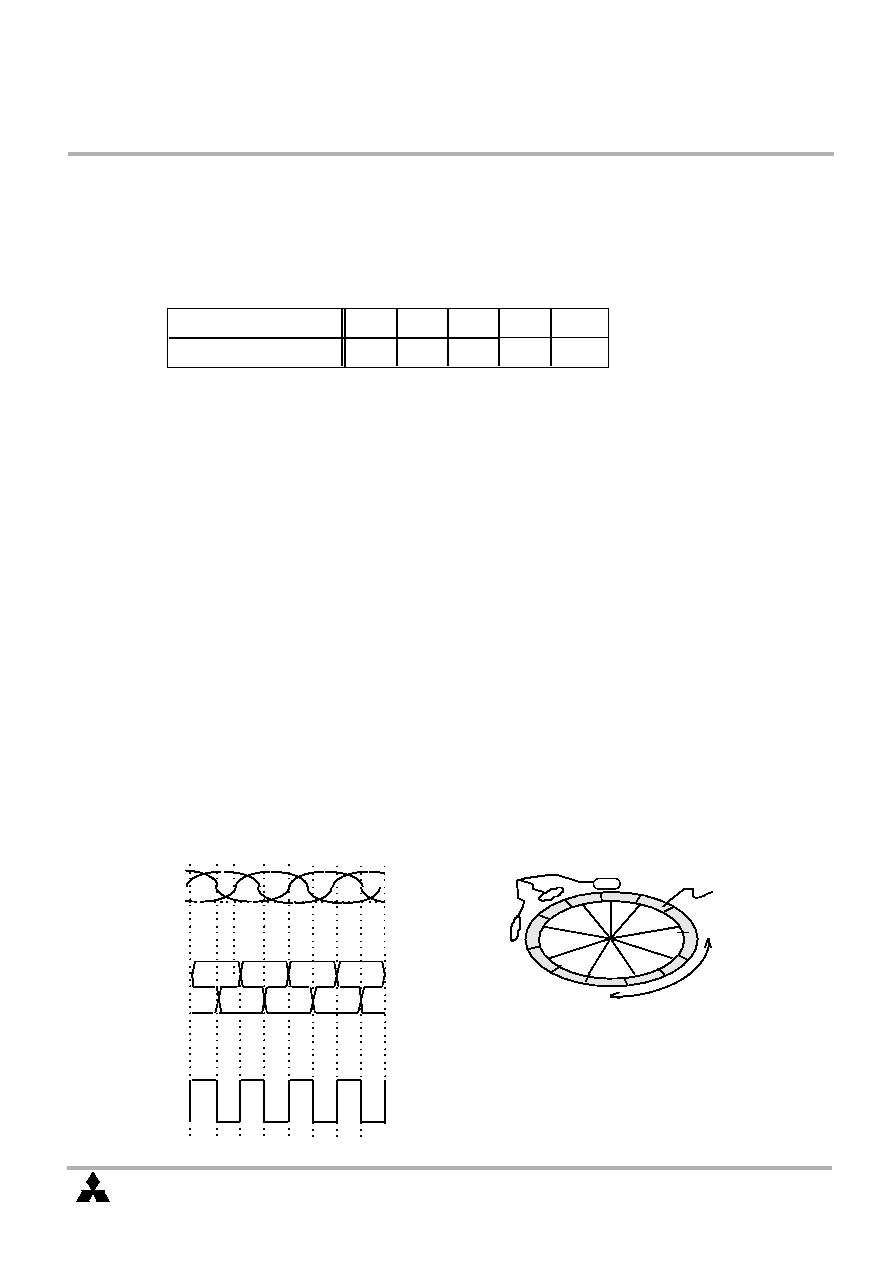
Time
carrier period
Motor current
Control value
Io=Vrs / Rs
Control value
Current
path 1
Current
path 2
Direct PWM operation
FORWARD Current path timing 2.
Current path 2
M
Rs
VM23
RSL
SL+
SL-
GND
FORWARD Current path timing 1.
M
Current path 1
Rs
VM23
RSL
SL+
SL-
GND
The spindle and the slide channel is controlled by the direct PWM control.
Analog input voltage control the driving current which is in proportion to input voltage.
This control is direct PWM control type of motor current chopper.
Also,built-in the current limit circuit. This IC controls the motor current directly.
direct PWM operation as follows;
1) The current which flows on a motor is detected, and current is supplied
from a power supply until it reaches the predetermined instruction value
to which the current is proportional to input voltage.
2) When current reaches an instruction value, an output transistor is changed and
the period coil inertia energy to a career cycle is made to regeneration using an internal path.
3) After repeat 1) and 2).
Therefore, the IC constantly surveillance and control the current value itself use sensor resistor.
Moreover, these ICs built-in current limit circuit so that protect to large current.
Thus, if input excessive control voltage, the current don't flow that settle limit current.
12
M63016FP
Spindle Motor AND 4CH ACTUATOR Drive IC
MITSUBISHI SEMICONDUCTORS
MITSUBISHI ELECTRIC CORPORATION
REV.011126
20
PWM carrier frequency setting
PWM carrier frequency is decided by charging and discharging the capacitor that is connected to OSC terminal
outer IC. Examination of the relationship the capacitor connected to OSC terminal and PWM carrier frequency
is given in following table.
Capacitor [pF]
330
220
65
90
130
140
Carrier Frequency [KHz]
110
160
*note) This PWM carrier frequency is TYP value.
180
110
Recommendation of SHORT BRAKE MODE at Spindle DRIVE
This IC has two brake mode, PWM-BRAKE-MODE and SHORT-BRAKE-MODE. IN this IC recommendation,
SHORT-BRAKE-MODE is superior to PWM-BRAKE-MODE to reducing the power dissipation and to avoid breaking
down of this IC.
(By excessive reverse torque current IN braking a Motor with PWM-BRAKE from high-speed-rotation with being
excessive Back-EMF, this IC could be broken.)
The relationship between the hall elements, the Motor output current and FG output(18pulse/rotation)
are shown in bellow Figure.
Hw+
Hv+
Hu+
U
W
V
U
W
V
U
W
V
Output
current
+
0
-
FG
output
U
V
W
U
V
W
V
U
W
FORWARD
Spin > REF
REVERSE
Spin < REF
Outer rotor
The relationship between hall-amplifier-input and output-current-commutation/FG output at Spindle DRIVE
Hall elements
Hall
input
13

M63016FP
Spindle Motor AND 4CH ACTUATOR Drive IC
MITSUBISHI SEMICONDUCTORS
MITSUBISHI ELECTRIC CORPORATION
REV.011126
20
FG function at Spindle DRIVE
The FG terminal outputs the square pulse signal synchronizing with the Hall inputs [Hu+,Hu-,
Hv+, Hv-,Hw+,Hw-] timing.And, the FG terminal is open-collector output.
(cf.FG timing chart on the previous page)
Phase delay circuit at Slide
Phase delay circuit is built in the IC to detect an output spike current, when the Motor current
direction is switching.
IN switching the Motor current direction, Phase delay circuit switch-off all output transistor of H-
bridge for 3usec.
Output current setting at Slide
IN this IC, since output transistor is NPN-type transistor, Motor coil current (Io) is larger than
sensing resistance current about 20mA (TYP.) according to base current of output transistor.
Therefore please design output current with consisting these base current.
14
M63016FP
Spindle Motor AND 4CH ACTUATOR Drive IC
MITSUBISHI SEMICONDUCTORS
MITSUBISHI ELECTRIC CORPORATION
REV.011126
20
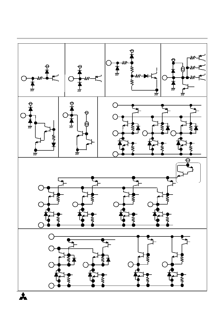
[I/O circuit]
FOIN,TOIN,Spin
LOIN+,LOIN-
Opin,REF
5VCC
2K
Hu+,Hu-
Hv+,Hv-
Hw+,Hw-
5VCC
2K
MU1,MU2,MU3
HB
FG
VM1,RSP,U,V,W
VM1
RSP
U
V
W
GND
OSC
VM23,RSL,SL+,SL,LO+,LO-
VM23
RSL
SL+
SL-
GND
LO+
LO-
5VCC,FO+,FO,TO+,TO-
5VCC
FO+
FO-
GND
TO+
TO-
REG
VM1
9V Max
5VCC
5VCC
2K
8K
30K
10K
5VCC
2K
2K
2K
5VCC
5VCC
VM1
15

M63016FP
Spindle Motor AND 4CH ACTUATOR Drive IC
MITSUBISHI SEMICONDUCTORS
MITSUBISHI ELECTRIC CORPORATION
REV.011126
20
Glass-epoxy FR-4
thickness
Size
material : copper
Board material
70X70mm
t=1.6mm
1 and 2 layers
Thickness:t=
18um
N-type
board
[2 layer]
O-type
board
[2 layer]
P-type
board
[1 layer]
1st layer [TOP view]
2nd layer [BACK view]
[The boards for thermal dera ting evaluation]
POWER-SSOP
42P9R-B
Evaluation board
mounted IC
Chip
Heat sinkLead
16

M63016FP
Spindle Motor AND 4CH ACTUATOR Drive IC
MITSUBISHI SEMICONDUCTORS
MITSUBISHI ELECTRIC CORPORATION
REV.011126
20
[The Notes on designing the layout of the board]
This IC has direct PWM controls for the Spindle channel and the Slide channel drive, therefore the circuits of the IC are
influenced more easily by the PWM switching noise than those have linear controls. Please refer to the following
notes on the occasion of designing the layout pattern of the board on which the IC is mounted.
note1
I t is necessary for some application in order to reduce the PWM noise that pass condensers are connected
between power supply pins(VM23:4pin, VM1:22pin, 5VCC:39pin) and GND pin, even if the power
supplies of the application already have pass condensers. The closer the connection points of the condensers are
to the pins, the more effective it is to reduce the noise.
Please refer to the values of the condensers on the page of [An example of the values of the external parts.]
(The value of the condensers is only a reference value. It differs in each application because the bad influence of
PWM noise relates to the layout pattern of the board.)
note2
The feedback point of the Spindle channel [the Slide channel] is the connected point to the VM1(22pin)
[the VM23(4pin)] line from the RSP(15pin) [RSL(8pin)] pin through the sensing resistor RSP[RSL]. Therefore
the closer the feedback point is to the power supply pin, the more stable the circuits are for the PWM noise.
cf. [application circuit]
note3
The farther the large current output lines(especially PWM output lines of the Spindle CH. and the Slide CH.) which
are indicated as wide lines in the Fig. [application circuit] are to the small signal input lines, the less the bad influence
of the PWM noise comes to be without the cross-talk between a large current output line and a small input signal line.
17

M63016FP
Spindle Motor AND 4CH ACTUATOR Drive IC
MITSUBISHI SEMICONDUCTORS
MITSUBISHI ELECTRIC CORPORATION
REV.011126
20
[The Notes on designing the layout of the board]
note5
The closer the GND side of the capacitor connected with OSC pin (30 pin) is to the GND pin(33pin), which is the nearest
GND to the GND of the small signal circuit inside the IC, the less the bad influence of the PWM noise on the GND line
comes to be.
cf. [application circuit]
note4
IN case the PWM switching noise influences the REF input, it is necessary for some application that a condenser is
connected between REF pin(25pin) and GND pin. The closer the connection points of the condensers are to the pins,
the more effective it is to reduce the noise. (This is the same as note1.)
cf.[application circuit], [An example of the values of the external parts]
18
M63016FP
Spindle Motor AND 4CH ACTUATOR Drive IC
MITSUBISHI SEMICONDUCTORS
MITSUBISHI ELECTRIC CORPORATION
REV.011126
20
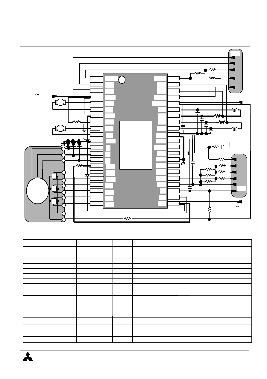
[APPLICATION CIRCUIT1]
External Parts Name
Typ. value
Unit
Note
RSP
0.33
ohm
Ilim1F=1.5[A], Ilim1R=1.0[A], gain=3.0[A/V]
RSL
0.5
ohm
Ilim=1.0[A], gain=2.0[A/V]
RFO, RTO
0.33
ohm
gain=1.2[A/V]
Rh
200
ohm
R1, R2, R3, R4, R5, R6
10
K ohm
R7, R8
10
K ohm
R9, R10
10
K ohm
C1
330
pF
C2
180
pF
FOSC=110KHz
C3
0.1 - 0.01
uF
Capacitors against output oscillation in a cold atmosphere
D1
-
-
Shottky Diode (VF<0.5V at IL=1.0A recommend)
C4, C5, C6
10 - 33
uF
Pass condenser for power supply
C7
0.1
uF
REF input noise filter condenser
[An example of the values of the external parts]
*These values are only examples, not the guaranteed values. And the values differ IN each application.
(The Shottky diodes are not necessary in some application.
cf. note1,note2 in page(4/22)
(The capacitor is not necessary in some application. )
Slide, Loading
1
2
3
4
5
6
7
8
9
10
11
12
13
14
15
16
17
18
25
26
27
28
29
30
31
32
33
34
35
36
37
38
39
40
41
42
M63
0
1
6
FP
19
20
21
22
23
24
GND
OPIN-
GND
GND
OSC
RFO
VM23
MU3
LO+
LO-
RSL
SL+
SL-
W
V
U
RSP
HW-
HW+
HV-
HV+
HU-
HU+
VM1
HB
FG
REF
MU1
MU2
FOIN
SPIN
TOIN
LOIN+
FO-
TO+
TO-
SLIN
TS
FS
Loading
10K
*Pull-up
Resistance
6v 12v
DSP
MCU
M
M
Slide
GND
5VCC
FO+
5V
1.65v
RS L
RSP
R1
R2
R3
R4
5 12v
C1
LOIN-
RTO
C2
M
RTO
RFO
R5
R6
R7
R8
R9
R10
Rh
R9
C5
C4
C6
C7
C3
C3
C3
C3
D1D1
D1
+
+
+
SBD
(The capacitors are not necessary in some application.)
C8
480
pF
FG output noise filter condenser
C8
19

M63016FP
Spindle Motor AND 4CH ACTUATOR Drive IC
MITSUBISHI SEMICONDUCTORS
MITSUBISHI ELECTRIC CORPORATION
REV.011126
20
Slide, Loading
1
2
3
4
5
6
7
8
9
10
11
12
13
14
15
16
17
18
25
26
27
28
29
30
31
32
33
34
35
36
37
38
39
40
41
42
M63
0
1
6
FP
19
20
21
22
23
24
GND
OPIN-
GND
GND
OSC
RFO
VM23
MU3
LO+
LO-
RSL
SL+
SL-
W
V
U
RSP
HW-
HW+
HV-
HV+
HU-
HU+
VM1
HB
FG
REF
MU1
MU2
FOIN
SPIN
TOIN
LOIN+
FO-
TO+
TO-
SLIN
TS
FS
Loading
10K
*Pull-up
resistance
6v 12v
DSP
MCU
M
M
Slide
GND
5VCC
FO+
5V
1.65v
RS L
RSP
R1
R2
R3
R4
5 12v
C1
LOIN-
RTO
C2
M
RTO
RFO
R5
R6
R7
R8
R9
R10
Rh
R9
C5
C4
C6
C7
C3
C3
C3
C3
D1D1
D1
+
+
+
SBD
C8
External Parts Name
Typ. value
Unit
Note
RSP
0.33
ohm
Ilim1F=1.5[A], Ilim1R=1.0[A], gain=3.0[A/V]
RSL
0.5
ohm
Ilim=1.0[A], gain=2.0[A/V]
RFO, RTO
0.33
ohm
gain=1.2[A/V]
Rh
200
ohm
R1, R2, R3, R4, R5, R6
10
K ohm
R7, R8
10
K ohm
R9, R10
10
K ohm
C1
330
pF
C2
180
pF
Fosc=110KHz
C3
0.1 - 0.01
uF
D1
-
-
Shottky Diode (VF<0.5V at IL=1.0A recommend)
C4, C5, C6
10 - 33
uF
Pass condenser for power supply
C7
0.1
uF
[An example of the values of the external parts]
*These values are only examples, not the guaranteed values. And the values differ IN each application.
(The Shottky diodes are not necessary in some application.
cf. note1,note2 in page(3/20)
)
(The capacitor is not necessary in some application. )
(The capacitors are not necessary in some application.)
C8
480
pF
FG output noise filter condenser
Capacitors against output oscillation in a cold atmosphere
REF input noise filter condenser
[APPLICATION CIRCUIT2] M63015FP same condition
20