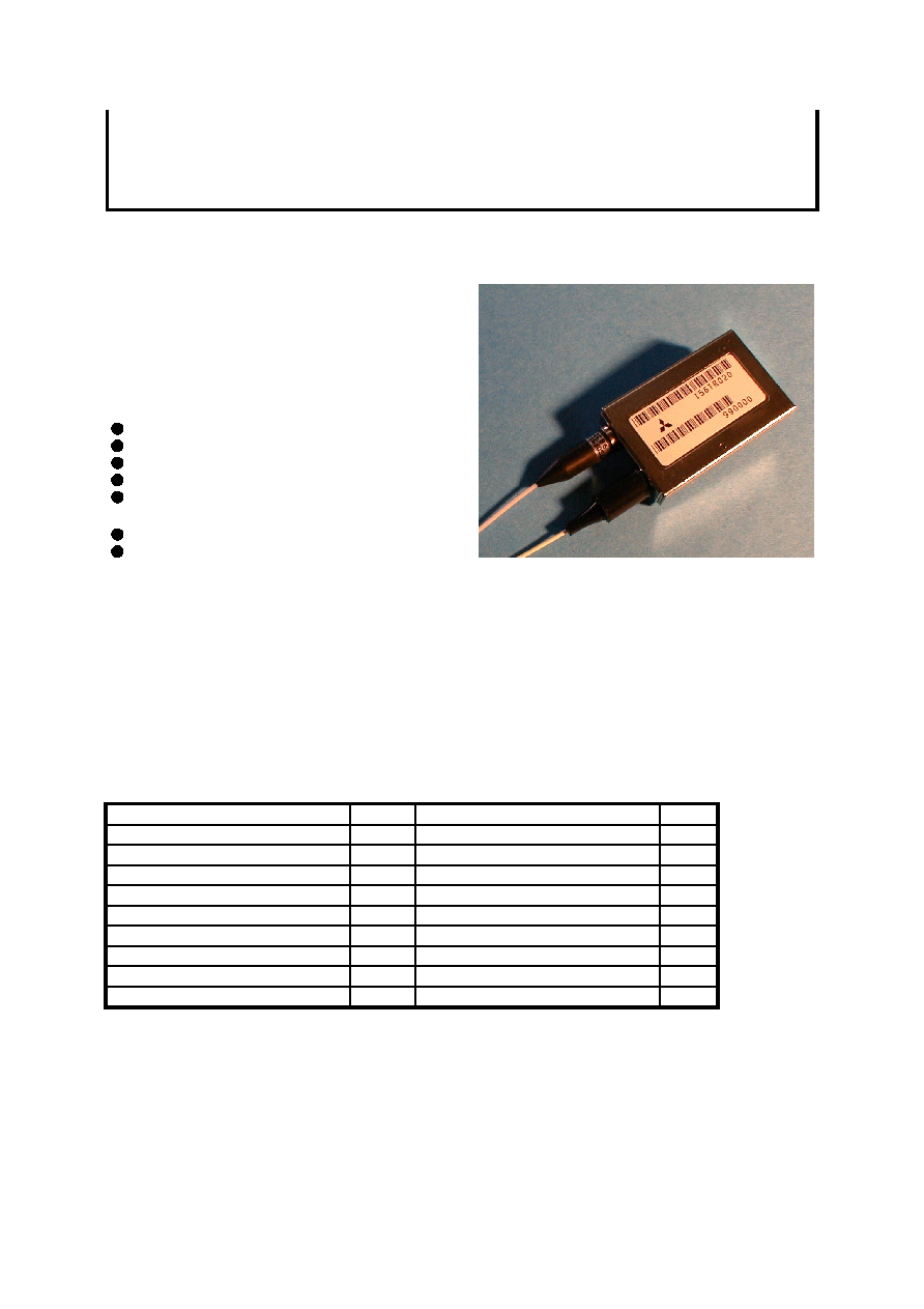
MITSUBISHI (OPTICAL DEVICES)
MF-156DS-TR123-030/040/050
SONET/SDH TRANSCEIVER
DESCRIPTION
This product is designed to provide high optical
performance for SDH STM-1/SONET OC-3.
Transmitter uses uncooled laser in a hermetic pigtail
coaxial module with drivered by specific integrated
circuit.
Receiver uses PIN preamp in a hermetic pigtail
coaxial module and integrated circuits for reshaping,
retiming and regenerating optical signal.
FEATURES
Tx + Rx combined
Full SONET/SDH line up
Low voltage, low power consumption, low cost
20-PIN DIP with fiber pigtail
Single +3.3V power supply and P-ECL compatible
input and output
Temp range:-40 to 85
∞
C
Clock recovery
APPLICATION
Short haul and long haul telecommunication systems
for SDH STM-1 / SONET OC-3.
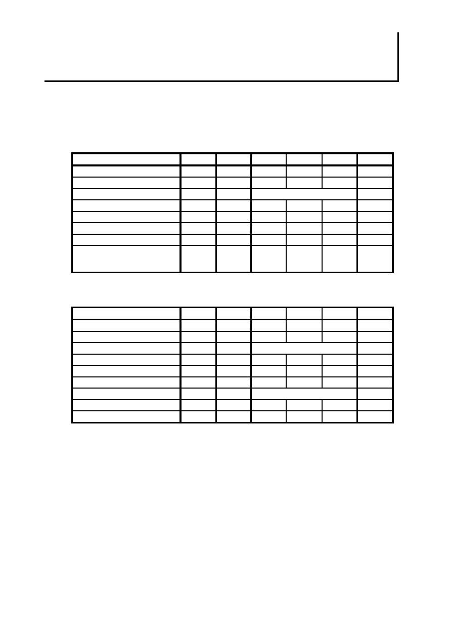
ABSOLUTE MAXIMUM RATINGS
Stress below listed absolute maximum rating may cause permanent damage to the transceiver.
Th is is a stress o nly and functional operation of the transceiver at these or any other conditions in excess of those
given in the operational sections of this data sheet is not implied.
Exposure to Absolute Maximum Rating for extended periods may affect transceiver reliability.
(TC=25
∞
C)
Parameter
Symbol
Rating
Unit
Supply voltage
Vcc
5.0
V
PECL high output current
-
30
mA
PECL input voltage
-
0 to Vcc
V
Storage temperature
Tstg
-40 to 85
∞
C
Operating case temperature
Tc
-40 to 85
∞
C
Soldering Temperature
-
+250
∞
C
Soldering Time
-
10
sec
Relative humidity(non condensation)
-
5 to 85
%
Fiber bend radius
rF
30
mm
MITSUBISHI (OPTICAL DEVICES)
MF-156DS-TR123-030/040/050
SONET/SDH TRANSCEIVER
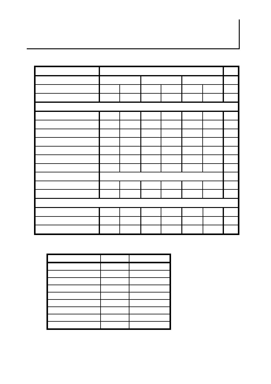
ELECTRICAL CHARACTERISTICS
All parameters are specified over the operating case temperature.
Measurement conditions are at 155.52Mb/s+/-20ppm, NRZ PN2
23
-1 and 50%duty cycle data signal.
Vcc=+3.3V+/-5%, Tc=-40 to 85
∞
C, Using a PRBS 2
23
-1 pattern with a 50% Mark ratio, unless otherwise noted.
Transmitter
Parameters
Condition
Symbol
Min.
Typ.
Max.
Unit
Supply voltage
Vcc
3.135
3.3
3.465
V
Power consumption
Pc
-
230
610
mW
Input voltage
note 1
-
LVPECL(*)
-
Transmitter disable voltage
note 2
-
Vcc-1.165
-
Vcc
V
Transmitter enable voltage
note 2
-
0
-
0.8
V
Laser bias monitor voltage
note 3
-
-
-
0.55
V
Laser backface monitor voltage
note 3
-
-
-
0.20
V
Laser bias monit or and Laser
backface monitor common mode
voltage
note 3
-
0.0
-
3.0
V
Receiver
Parameters
Condition
Symbol
Min.
Typ.
Max.
Unit
Supply voltage
Vcc
3.135
3.3
3.465
V
Power consumption
Pc
-
500
700
mW
Output voltage
note 4
-
LVPECL(*)
-
Data/Clock external Load
note 4
RI
50
-
-
ohm
Data to clock phase
note 5
-
-0.8
-
+0.8
nsec.
Clock duty
note 5
-
45
-
55
%
SD output voltage
note 6
-
LVTTL(*)
-
SD activation time
note 7
Tact
-
-
95
us
SD deactivation time
note 7
Tdeact
-
-
300
ms
(*): Values shown are for Vcc=3.3V Level specifications will vary 1:1 with Vcc
MITSUBISHI (OPTICAL DEVICES)
MF-156DS-TR123-030/040/050
SONET/SDH TRANSCEIVER
OPTICAL CHARACTERISTICS
Parameter
Specification
Unit
ITU code
S-1.1(*)
L-1.1
L-1.2(*)
Min.
Max.
Min.
Max.
Min.
Max.
Optical Budget
0
14
10
29
10
29
dB
Transmitter
Wavelength
1261
1360
1280
1335
1480
1580
nm
Optical power at pigtail
-14
-8
-4
0
-4
0
dBm
Optical power when disable
-
-45
-
-45
-
-45
dBm
Spectral width(rms)
-
4
-
-
-
-
nm
Spectral width(-20dB)
-
-
-
1
-
1
nm
SMSR
-
-
30
-
30
-
dB
Extinction ratio
8.2
-
10
-
10
-
dB
Optical wave form
ITU Mask compliant
-
Path penalty
-
1
-
1
-
1
dB
Dispersion
-
100
-
185
-
1900
ps/nm
Receiver
Sensitivity
-
-34
-
-34
-
-34
dBm
Overload
-8(#)
-
-8(#)
-
-8(#)
-
dBm
Wavelength
1260
1580
1260
1580
1260
1580
nm
(*): Under development (#): target 0dBm
ORDERING INFORMATION
Part number
ITU-code
Optical connector type
MF-156DS-TR123-030
S-1.1
FC/FC
MF-156DS-TR123-031
S-1.1
SC/SC
MF-156DS-TR123-032
S-1.1
ST/ST
MF-156DS-TR123-040
L-1.1
FC/FC
MF-156DS-TR123-041
L-1.1
SC/SC
MF-156DS-TR123-042
L-1.1
ST/ST
MF-156DS-TR123-050
L-1.2
FC/FC
MF-156DS-TR123-051
L-1.2
SC/SC
MF-156DS-TR123-052
L-1.2
ST/ST

MITSUBISHI (OPTICAL DEVICES)
MF-156DS-TR123-030/040/050
SONET/SDH TRANSCEIVER
TRANSCEIVER PIN ALLOCATION
No.
Symbol
Description
No.
Symbol
Description
1
PDB
No user connection
20
LBF+
Laser-backface monitor(+)
2
SD
Signal detect
19
LBF-
Laser-backface monitor(-)
3
NUC
No user connection
18
LBS+
Laser-bias monitor(+)
4
GND
Ground
17
LBS-
Laser-bias monitor(-)
5
VCC
Vcc
16
TDT-
Tx data(-)
6
RCK-
Rx clock(-)
15
TDT+
Tx data(+)
7
RCK+
Rx clock(+)
14
GND
Ground
8
RDT-
Rx data(-)
13
TD
Transmit disable
9
RDT+
Rx data(+)
12
Vcc
Vcc
10
NUC
No user connection
11
NUC
No user connection
NOTE: NUC pin: OPEN (don't connect)
GENERAL OUTLINE DRAWING
Transmitter / Receiver (FC/PC, SC/PC and ST/PC connector are available)
NOTE: TOLERANCES UNLESS NOTED +/-0.5
DIMENSIONS ARE IN MILLIMETERS
L=550+/-100
MITSUBISHI (OPTICAL DEVICES)
MF-156DS-TR123-030/040/050
SONET/SDH TRANSCEIVER
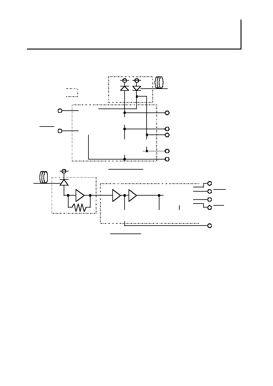
BLOCK DIAGRAM
Alarm
PLL
DATAout
DATAout
CLKout
CLKout
Signal Detect
OPT. IN
Receiver Part
Decider
Clock recovery IC
Amp
Preamp
PD-Preamp Module
PD
LD Module
Driver IC
A.P.C
DATAin
DATAin
DRIVER IC
PD
LD
Laser-backface monitor(+)
Laser-backface monitor(-)
Laser-bias monitor(+)
Laser-bias monitor(-)
Transmitter disable
integrated device
OPT. OUT
Transmitter Part
VCC
VCC