
MOSEL VITELIC
1
V53C518160A
1M x 16 FAST PAGE MODE
CMOS DYNAMIC RAM
V53C518160A Rev. 1.3 March 1998
HIGH PERFORMANCE
50
60
Max. RAS Access Time, (t
RAC
)
50 ns
60 ns
Max. Column Address Access Time, (t
CAA
)
25 ns
30 ns
Min. Fast Page Mode Cycle Time, (t
PC
)
35 ns
40 ns
Min. Read/Write Cycle Time, (t
RC
)
90 ns
110 ns
Features
s
1MB x 16-bit organization
s
Fast Page Mode for a sustained data rate
of 29 MHz
s
RAS access time: 50, 60 ns
s
Dual CAS Inputs
s
Low power dissipation
s
Read-Modify-Write, RAS-Only Refresh,
CAS-Before-RAS Refresh, Self Refresh
� Refresh Interval: 1024 cycles/16 ms
s
Available in 42-pin 400 mil SOJ and
44/50-pin 400 mil TSOP-II Packages
s
Single 5V
�
10% Power Supply
s
TTL Interface
Description
The V53C518160A is a 1048576 x 16 bit high-
performance CMOS dynamic random access
memory. The V53C518160A offers Fast Page
mode operation. The V53C518160A has symmet-
ric address, 10-bit row and 10-bit column.
All inputs are TTL compatible. Fast Page Mode
operation allows random access up to 1024 x 16
bits, within a page, with cycle times as short as
35ns.
These features make the V53C518160A ideally
suited for a wide variety of high performance com-
puter systems and peripheral applications.
Device Usage Chart
Operating
Temperature
Range
Package Outline
Access Time (ns)
Power
Temperature
Mark
K
T
50
60
Std.
0
�
C to 70
�
C
�
�
�
�
�
Blank
�40
�
C to +85
�
C
�
�
�
�
�
I
2
V53C518160A Rev. 1.3 March 1998
MOSEL VITELIC
V53C518160A
Pin Names
A
0
�A
9
Row, Column Address Inputs
RAS
Row Address Strobe
UCAS
Column Address Strobe/Upper Byte Control
LCAS
Column Address Strobe/Lower Byte Control
WE
Write Enable
OE
Output Enable
I/O
1
�I/O
16
Data Input, Output
V
CC
+5V Supply
V
SS
0V Supply
NC
No Connect
Description
Pkg.
Pin Count
TSOP-II
T
44/50
SOJ
K
42
V
CC
I/O
1
I/O
2
I/O
3
I/O
4
VCC
I/O
5
I/O
6
I/O
7
I/O
8
NC
NC
WE
RAS
NC
NC
A0
A
1
A
2
A
3
V
CC
V
SS
I/O
16
I/O
15
I/O
14
I/O
13
V
SS
I/O
12
I/O
11
I/O
10
I/O
9
NC
LCAS
UCAS
OE
A
9
A
8
A
7
A
6
A
5
A
4
V
SS
5
6
7
8
9
10
11
12
1
2
3
4
40
39
38
37
36
35
34
33
32
31
30
29
13
14
15
16
17
18
19
20
28
27
26
25
24
23
22
42
21
41
V
CC
I/O
1
I/O
2
I/O
3
I/O
4
VCC
I/O
5
I/O
6
I/O
7
I/O
8
NC
NC
NC
WE
RAS
NC
NC
A0
A
1
A
2
A
3
V
CC
V
SS
I/O
16
I/O
15
I/O
14
I/O
13
V
SS
I/O
12
I/O
11
I/O
10
I/O
9
NC
NC
LCAS
UCAS
OE
A
9
A
8
A
7
A
6
A
5
A
4
V
SS
5
6
7
8
9
10
11
1
2
3
4
15
16
17
18
19
20
511816500-02
21
22
23
24
25
46
45
44
43
42
41
40
50
49
48
47
36
35
34
33
32
31
30
29
28
27
26
42-Pin Plastic SOJ
PIN CONFIGURATION
Top View
44/50-Pin Plastic TSOP-II
PIN CONFIGURATION
Top View

3
V53C518160A Rev. 1.3 March 1998
MOSEL VITELIC
V53C518160A
Block Diagram
No. 2 Clock
Generator
Data In
Buffer
Data Out
Buffer
Column
Address
Buffers (10)
Refresh
Controller
Row
Decoder
Refresh
Counter (10)
Voltage Down
Generator
No. 1 Clock
Generator
Row
Address
Buffers (10)
10
16
I/O1 I/O2
I/O16
16
VCC
VCC (internal)
OE
10
10
10
16
1024
1024
x16
Memory Array
1024 x 1024 x 16
Sense Amplifier
I/O Gating
316516500-03
Column
Decoder
A0
UCAS
WE
LCAS
A1
A2
A3
A4
A5
A6
A7
A8
A9
RAS
10
� � �
Absolute Maximum Ratings*
*
Note:
Stresses greater than those listed under "Absolute Maximum Ratings" may cause permanent damage to the device. This is a
stress rating only and functional operation of the device at these or any other conditions above those indicated in the operational
sections of this specification is not implied. Exposure to absolute maximum rating conditions for extended periods may affect
reliability.
Capacitance*
T
A
= 25
�
C, V
CC
= 5 V
�
10%, V
SS
= 0 V, f = 1 MHz
*
Note:
Capacitance is sampled and not 100% tested.
Symbol
Parameter
Commercial
Extended
Units
V
N
Power Supply Voltage
-1 to +7
-1 to +7
V
V
DQ
Input/Output Voltage
-0.5 to min (V
CC
+0.5, 7.0)
-0.5 to min (V
CC
+0.5, 7.0)
V
T
BIAS
Temperature Under Bias
-10 to +125
-65 to +135
�
C
T
STG
Storage Temperature
-55 to +125
-65 to +150
�
C
Symbol
Parameter
Min.
Max.
Unit
C
IN1
Address Input
--
5
pF
C
IN2
RAS, UCAS, LCAS,
WE, OE
--
7
pF
C
OUT
Data Input/Output
--
7
pF
4
V53C518160A Rev. 1.3 March 1998
MOSEL VITELIC
V53C518160A
DC and Operating Characteristics
(1-2)
T
A
= 0
�
C to 70
�
C, V
CC
= 5 V
�
10%, V
SS
= 0 V, t
T
= 2ns, unless otherwise specified.
Symbol
Parameter
Access
Time
Commercial
Unit
Test Conditions
Notes
Min.
Max.
I
LI
Input Leakage Current
(any input pin)
�10
10
m
A
V
SS
�
V
IN
�
V
CC
+ 0.5V
1
I
LO
Output Leakage Current
(for High-Z State)
�10
10
m
A
V
SS
�
V
OUT
�
V
CC
+ 0.5V
RAS, CAS at V
IH
1
I
CC1
V
CC
Supply Current,
Operating
50
200
mA
t
RC
= t
RC
(min.)
2, 3, 4
60
180
I
CC2
V
CC
Supply Current,
TTL Standby
2
mA
RAS, CAS at V
IH
other inputs
�
V
SS
I
CC3
V
CC
Supply Current,
RAS-Only Refresh
50
200
mA
t
RC
= t
RC
(min.)
2, 4
60
180
I
CC4
V
CC
Supply Current,
Fast Page Mode
50
55
mA
Minimum Cycle
2, 3, 4
60
50
I
CC5
V
CC
Supply Current,
during CAS-before-RAS Refresh
50
200
mA
t
RC
= t
RC
(min.)
2, 4
60
180
I
CC6
V
CC
Supply Current,
CMOS Standby
1.0
mA
RAS
�
V
CC
� 0.2 V,
CAS
�
V
CC
� 0.2 V
other input
�
V
SS
1
I
CC7
Self Refresh
1.0
mA
CBR cycle with
t
RAS
�
t
RASS (min.)
,
CAS Held Low,
WE = V
CC
-0.2V, Address and
D
IN
= V
CC
-0.2V or 0.2V
V
CC
Power Supply Voltage
4.5
5.5
V
V
IL
Input Low Voltage
�0.5
0.8
V
1
V
IH
Input High Voltage
2.4
V
CC
+0.5
V
1
V
OL
Output Low Voltage
0.4
V
I
OL
= 4.2 mA
1
V
OH
Output High Voltage
2.4
V
I
OH
= �5.0 mA
1
5
V53C518160A Rev. 1.3 March 1998
MOSEL VITELIC
V53C518160A
AC Characteristics
(5,6)
T
A
= 0
�
C to 70
�
C, V
CC
= 5 V
�
10%, t
T
= 2ns, unless otherwise noted
#
Symbol
Parameter
Limit Values
Unit
Note
-50
-60
Min.
Max.
Min.
Max.
Common Parameters
1
t
RC
Random read or write cycle time
90
--
110
--
ns
2
t
RP
RAS precharge time
30
--
40
--
ns
3
t
RAS
RAS pulse width
50
10k
60
10k
ns
4
t
CAS
CAS pulse width
13
10k
15
10k
ns
5
t
ASR
Row address setup time
0
--
0
--
ns
6
t
RAH
Row address hold time
8
--
10
--
ns
7
t
ASC
Column address setup time
0
--
0
--
ns
8
t
CAH
Column address hold time
10
--
15
--
ns
9
t
RCD
RAS to CAS delay time
18
37
20
45
ns
10
t
RAD
RAS to column address delay
13
25
15
30
ns
11
t
RSH
RAS hold time
13
--
15
--
ns
12
t
CSH
CAS hold time
50
--
60
--
ns
13
t
CRP
CAS to RAS precharge time
5
--
5
--
ns
14
t
T
Transition time (rise and fall)
3
50
3
50
ns
7
15
t
REF
Refresh period
--
16
--
16
ms
Read Cycle
16
t
RAC
Access time from RAS
--
50
--
60
ns
8, 9
17
t
CAC
Access time from CAS
--
13
--
15
ns
8, 9
18
t
CAA
Access time from column address
--
25
--
30
ns
8,10
19
t
OAC
OE access time
--
13
--
15
ns
20
t
CAR
Column address to RAS lead time
25
--
30
--
ns
21
t
RCS
Read command setup time
0
--
0
--
ns
22
t
RCH
Read command hold time
0
--
0
--
ns
11
23
t
RRH
Read command hold time referenced to RAS
0
--
0
--
ns
11
24
t
CLZ
CAS to output in low-Z
0
--
0
--
ns
8
25
t
OFF
Output buffer turn-off delay
0
13
0
15
ns
12
26
t
OEZ
Output turn-off delay from OE
0
13
0
15
ns
12
27
t
DZC
Data to CAS low delay
0
--
0
--
ns
13
28
t
DZO
Data to OE low delay
0
--
0
--
ns
13
29
t
CDD
CAS high to data delay
10
--
13
--
ns
14
30
t
ODD
OE high to data delay
10
--
13
--
ns
14
6
V53C518160A Rev. 1.3 March 1998
MOSEL VITELIC
V53C518160A
Write Cycle
31
t
WCH
Write command hold time
8
�
10
�
ns
32
t
WP
Write command pulse width
8
�
10
�
ns
33
t
WCS
Write command setup time
0
�
0
�
ns
15
34
t
RWL
Write command to RAS lead time
13
�
15
�
ns
35
t
CWL
Write command to CAS lead time
13
�
15
�
ns
36
t
DS
Data setup time
0
�
0
�
ns
16
37
t
DH
Data hold time
10
�
10
�
ns
16
Read-modify-Write Cycle
38
t
RWC
Read-write cycle time
126
�
150
�
ns
39
t
RWD
RAS to WE delay time
68
�
80
�
ns
15
40
t
CWD
CAS to WE delay time
31
�
35
�
ns
15
41
t
AWD
Column address to WE delay time
43
�
50
�
ns
15
42
t
OEH
OE command hold time
13
�
15
�
ns
Fast Page Mode Cycle
43
t
PC
Fast page mode cycle time
35
�
40
�
ns
44
t
CP
CAS precharge time
10
�
10
�
ns
45
t
CPA
Access time from CAS precharge
�
30
�
35
ns
7
46
t
COH
Output data hold time
5
�
5
�
ns
47
t
RASP
RAS pulse width in fast page mode
50
200k
60
200k
ns
48
t
RHPC
CAS precharge to RAS Delay
30
�
35
�
ns
49
t
OES
OE setup time prior to
CAS
5
�
5
�
ns
Fast Page Mode Read-Modify-Write Cycle
50
t
PRWC
Fast page mode read-write cycle time
71
�
80
�
ns
51
t
CPWD
CAS precharge to WE
48
�
55
�
ns
CAS-before-RAS Refresh Cycle
52
t
CSR
CAS setup time
10
�
10
�
ns
53
t
CHR
CAS hold time
10
�
10
�
ns
54
t
RPC
RAS to CAS precharge time
5
�
5
�
ns
55
t
WRP
Write to RAS precharge time
10
�
10
�
ns
56
t
WRH
Write hold time referenced to RAS
10
�
10
�
ns
CAS-before-RAS Counter Test Cycle
57
t
CPT
CAS precharge time (CAS-before-RAS counter test cycle)
35
�
40
�
ns
#
Symbol
Parameter
Limit Values
Unit
Note
-50
-60
Min.
Max.
Min.
Max.
AC Characteristics
(Cont'd)

7
V53C518160A Rev. 1.3 March 1998
MOSEL VITELIC
V53C518160A
Self Refresh
58
t
REF
Self Refresh period
--
16
--
16
ms
59
t
RASS
RAS pulse width
100K
--
100K
--
ns
17
60
t
RPS
RAS precharge time
95
--
110
--
ns
17
61
t
CHS
CAS hold time
-50
--
-50
--
ns
17
#
Symbol
Parameter
Limit Values
Unit
Note
-50
-60
Min.
Max.
Min.
Max.

8
V53C518160A Rev. 1.3 March 1998
MOSEL VITELIC
V53C518160A
Notes:
1. All voltage are referenced to V
SS
.
2.
I
CC1
, I
CC3
, I
CC4
, and I
CC5
depend on cycle rate.
3.
I
CC1
and I
CC4
depend on output loading. Specified values are measured with the output open.
4.
Address can be changed once or less while RAS = V
IL
. In the case of I
CC4
it can be changed once or less during
an Fast page mode cycle.
5.
An initial pause of 200
m
s is required after power-up followed by 8 RAS cycles of which at least one cycle has to be
a refresh cycle, before proper device operation is achieved. In case of using internal refresh counter, a minimum of
8 CAS-before-RAS initialization cycles instead of 8 RAS cycles are required.
6.
AC measurements assume t
T
= 2ns.
7.
V
IH
(min.) and V
IL
(max.) are reference levels for measuring timing of input signals. Transition times are also
measured between V
IH
and V
IL
.
8.
Measured with the specified current load and 100pF at V
OL
= 0.8 V and V
OH
= 2.0 V. Access time is determined by
the latter of t
RAC
, t
CAC
, t
CAA
, t
CPA
, t
OAC
, t
CAC
is measured from tristate.
9.
Operation within the t
RCD (max.)
limit ensures that t
RAC
(max.)
can be met. t
RCD (max.)
is specified as a reference point
only. If t
RCD
is greater than the specified t
RCD (max.)
limit, then access time is controlled by t
CAC
.
10.
Operation within the t
RAD (max.)
limit ensures that t
RAC
(max.)
can be met. t
RAD (max.)
is specified as a reference point
only. If t
RAD
is greater than the specified t
RAD (max.)
limit, then access time is controlled by t
CAA
.
11.
Either t
RCH
or t
RRH
must be satisfied for a read cycle.
12.
t
OFF (max.)
, t
OEZ (max.)
define the time at which the outputs acheive the open-circuit condition and are not referenced
to output voltage levels. t
OFF
is referenced from the rising edge of RAS or CAS, whichever occurs last.
13.
Either t
DZC
or t
DZO
must be satisfied.
14.
Either t
CDD
or t
ODD
must be satisfied.
15.
t
WCS
, t
RWD
, t
CWD
, and t
AWD
are not restrictive operating parameters. They are included in the data sheet as electri-
cal characteristics only. If t
WCS
> t
WCS
(min.)
, the cycle is an early write cycle and data out pin will remain open-circuit
(high impedance) through the entire cycle; if t
RWD
> t
RWD (min.)
, t
CWD
> t
CWD (min.)
, and t
AWD
> t
AWD
(min.), the cycle
is a read-write cycle and I/O pins will contain data read from the selected cells. If neither of the above sets of con-
ditions is satisfied, the condition of the I/O pins (at access time) is indeterminate.
16.
These parameters are referenced to the CAS leading edge in early write cycles and to the WE leading edge in
read-write cycles.
17.
When using Self Refresh mode, the following refresh operations must be performed to ensure proper DRAM oper-
ation:
If row addresses are being refreshed on an evenly distributed manner over the refresh interval using CBR refresh
cycles, then only one CBR cycle must be performed immediately after exit from Self Refresh.
If row addresses are being refreshed in any other manner (ROR - Distributed/Burst; or CBR-Burst) over the refresh
interval, then a full set of row refreshes must be performed immediately before entry to and immediately after exit
from Self Refresh.

9
V53C518160A Rev. 1.3 March 1998
MOSEL VITELIC
V53C518160A
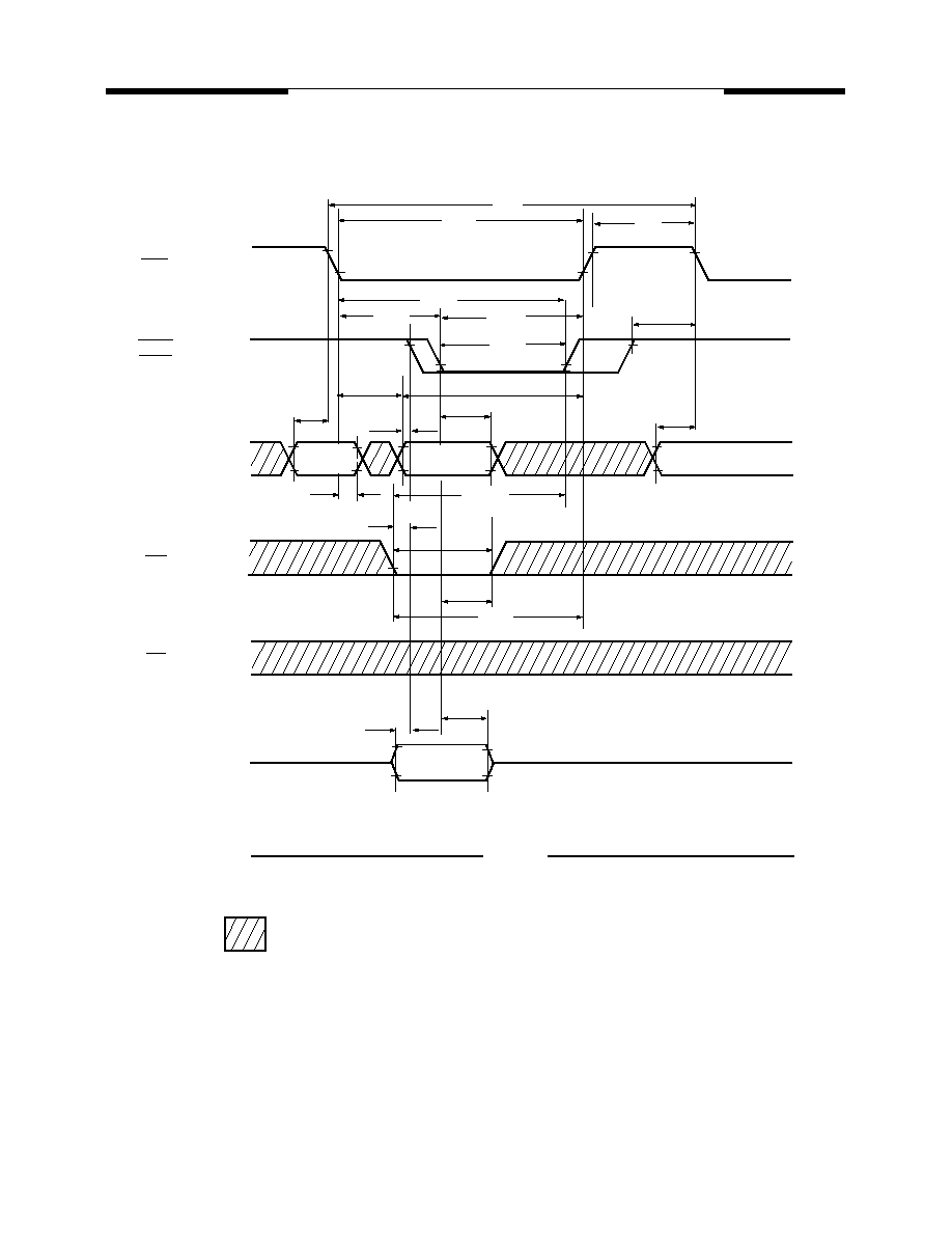
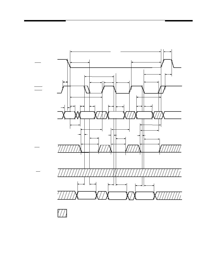
Waveforms of Read Cycle
Row
Column
Row
Valid Data Out
RAS
UCAS
Address
WE
OE
I/O
(Inputs)
I/O
(Outputs)
V
IH
V
IL
t
RAS
t
RC
t
CSH
t
RAD
t
CAS
t
RP
t
RAH
t
CRP
t
RSH
t
RCD
t
CAR
t
ASR
t
CAH
t
ASC
t
ASR
t
RCH
t
RRH
t
RCS
t
CAA
t
OAC
t
CLZ
t
CAC
t
OEZ
t
ODD
t
CDD
t
OFF
t
DZC
t
DZO
t
RAC
Hi Z
Hi Z
"H" or "L"
511816502-04
V
IH
V
IL
V
IH
V
IL
V
IH
V
IL
V
IH
V
IL
V
IH
V
IL
V
OH
V
OL
LCAS
10
V53C518160A Rev. 1.3 March 1998
MOSEL VITELIC
V53C518160A
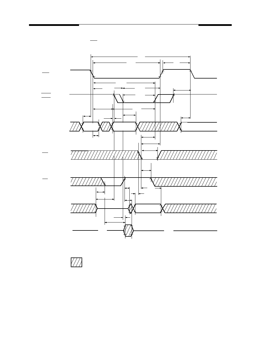
Waveforms of Write Cycle (Early Write)
RAS
Address
WE
OE
I/O
(Inputs)
I/O
(Outputs)
.
t
RAS
Valid Data In
Hi Z
Column
Row
Row
"H" or "L"
511816502-05
t
RC
t
RP
t
CSH
t
RCD
t
RSH
t
CAS
t
CRP
t
CAR
t
RAD
t
ASR
t
ASC
t
CAH
t
ASR
t
CWL
t
RAH
t
WCS
t
WP
t
WCH
t
RWL
t
DH
t
DS
V
IH
V
IL
V
IH
V
IL
V
IH
V
IL
V
IH
V
IL
V
IH
V
IL
V
IH
V
IL
V
OH
V
OL
UCAS
LCAS
11
V53C518160A Rev. 1.3 March 1998
MOSEL VITELIC
V53C518160A
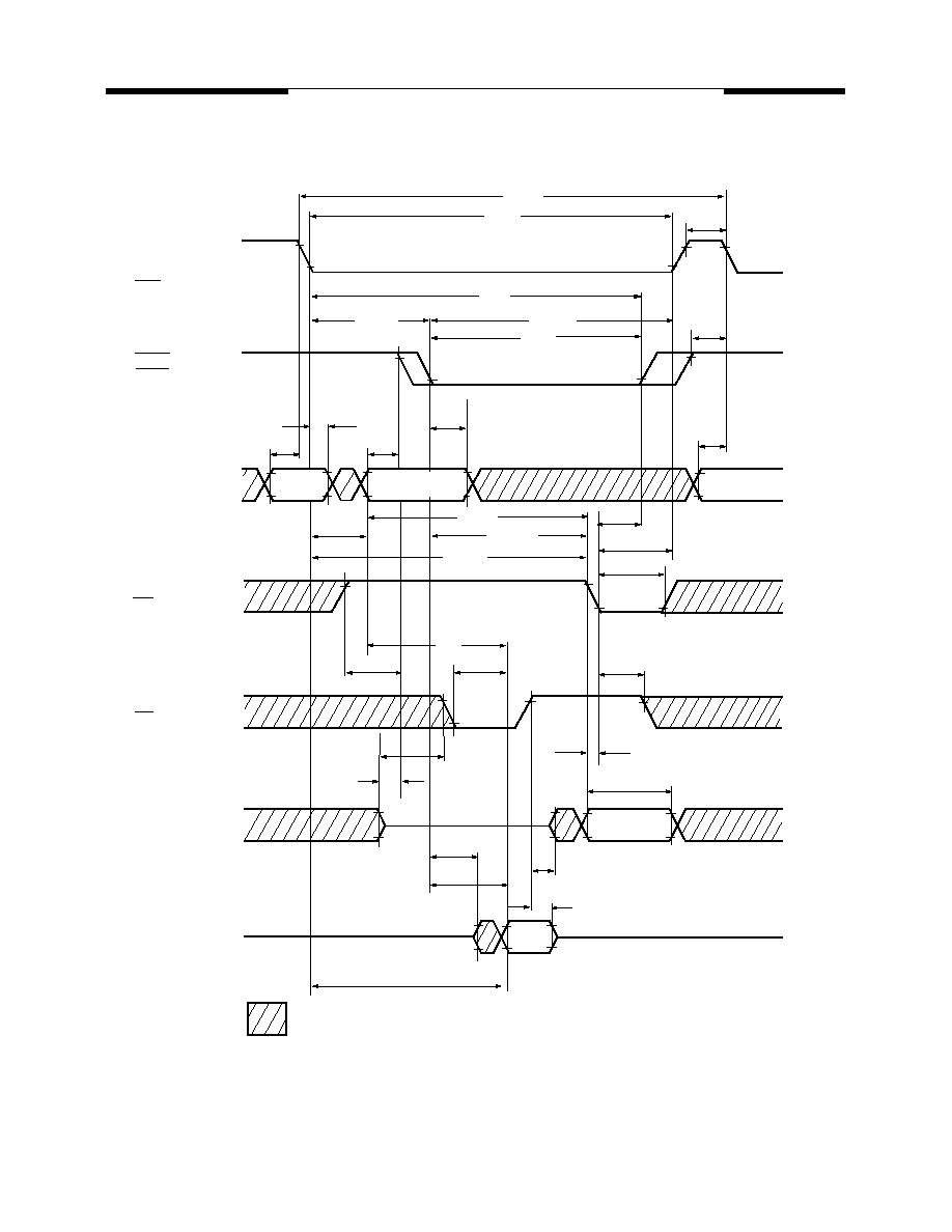
Waveforms of Write Cycle (OE Controlled Write)
Valid Data
t
RWL
t
WP
t
OEH
t
CWL
Row
"H" or "L"
Hi-Z
Hi-Z
Column
Row
t
ASC
t
RAD
t
CAR
t
CAH
t
RAH
RAS
Address
WE
OE
I/O
(Inputs)
I/O
(Outputs)
tCAS
tRSH
tRCD
t
ASR
t
ASR
511816502-06
V
IH
V
IL
V
OH
V
OL
V
IH
V
IL
V
IH
V
IL
V
IH
V
IL
V
IH
V
IL
V
IH
V
IL
t
RC
t
RAS
t
RP
t
CSH
t
CRP
t
ODD
t
DZO
t
DZC
t
DH
t
DS
t
OEZ
t
CLZ
t
OAC
UCAS
LCAS
12
V53C518160A Rev. 1.3 March 1998
MOSEL VITELIC
V53C518160A
Waveforms of Read-Write (Read-Modify-Write) Cycle
Row
Row
t
RWC
I/O
(Outputs)
I/O
(Inputs)
OE
WE
Column
Valid
Data in
Data
Out
t
RAC
"H" or "L"
RAS
Address
511816502-07
V
IH
V
IL
V
IH
V
IL
V
IH
V
IL
V
IH
V
IL
V
IH
V
IL
V
IH
V
IL
V
OL
V
OH
t
RAS
t
RP
t
CSH
t
RCD
t
RSH
t
CAS
t
CRP
t
ASR
t
CAH
t
ASC
t
RAH
t
ASR
t
RAD
t
AWD
t
CWD
t
RWD
t
CWL
t
RWL
t
WP
t
OEH
t
CAA
t
OAC
t
RCS
t
DS
t
DH
t
DZO
t
DZC
t
CLZ
t
CAC
t
ODD
t
OEZ
UCAS
LCAS

13
V53C518160A Rev. 1.3 March 1998
MOSEL VITELIC
V53C518160A
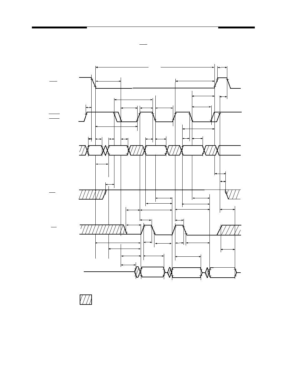
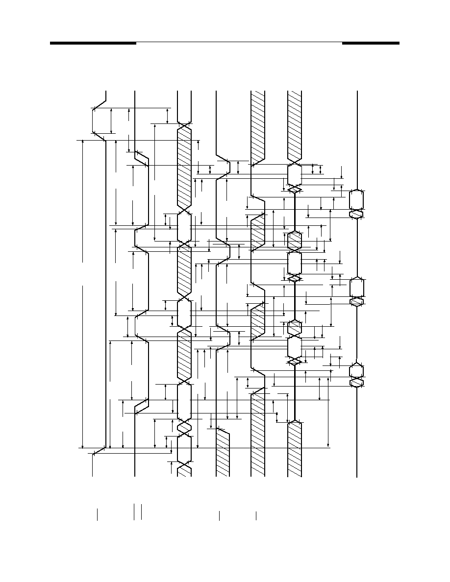
Waveforms of Fast Page Mode Read Cycle
tRP
Column 2
Row
Data Out
RAS
I/O
WE
Address
V
IH
V
IL
"H" or "L"
OE
t
RASP
(Output)
Data Out
Column N
Column 1
Data Out
1
2
N
511816502-08
V
IH
V
IL
V
IH
V
IL
V
IH
V
IL
V
OH
V
OL
V
IH
V
IL
t
RHPC
t
RCD
t
CRP
t
PC
t
CAS
t
CP
t
CAS
t
RSH
t
CAS
t
CRP
t
CSH
t
CAR
t
ASR
t
RAH
t
ASC
t
CAH
t
ASC
t
CAH
t
ASC
t
CAH
t
RAD
t
RCS
t
RRH
t
RCH
t
CAC
t
CAA
t
CPA
t
OES
t
CPA
t
CAA
t
OFF
t
OAC
t
RAC
t
CAC
t
CAA
t
CLZ
t
COH
t
COH
t
OEZ
t
CAC
UCAS
LCAS
14
V53C518160A Rev. 1.3 March 1998
MOSEL VITELIC
V53C518160A
Waveforms of Fast Page Mode Read Cycle (OE Control)
Column 2
Row
Data Out
RAS
I/O
WE
Address
"H" or "L"
OE
t
RASP
(Output)
Data Out
Column N
Column 1
Data Out
1
2
N
511816502
-09
V
IH
V
IL
V
IH
V
IL
V
IH
V
IL
V
IH
V
IL
V
OH
V
OL
V
IH
V
IL
t
RCD
t
RHPC
t
RP
t
CRP
t
RSH
t
CAS
t
CAS
t
CP
t
CAS
t
PC
t
CRP
t
CSH
t
CAR
t
ASR
t
RAH
t
ASC
t
CAH
t
ASC
t
CAH
t
ASC
t
CAH
t
RAD
t
RCS
t
RRH
t
RCH
t
CAC
t
CAC
t
CAA
t
CAA
t
CPA
t
CPA
t
OES
t
OFF
t
OEHC
t
OEHC
t
OAC
t
OEZ
t
OAC
t
OEP
t
OEZ
t
OAC
t
OEP
t
OEZ
t
CAC
t
CAA
t
RAC
t
CLZ
UCAS
LCAS

15
V53C518160A Rev. 1.3 March 1998
MOSEL VITELIC
V53C518160A
Waveforms of Fast Page Mode Read Cycle (WE Control)
Column 2
Row
Data Out
RAS
I/O
WE
Address
"H" or "L"
OE
t
RASP
(Output)
Data Out
Column N
Column 1
Data Out
1
2
N
511816502-10
V
IH
V
IL
V
IH
V
IL
V
IH
V
IL
V
IH
V
IL
V
OH
V
OL
V
IH
V
IL
t
RP
t
RCD
t
RHPC
t
PC
t
CRP
t
CAS
t
CP
t
CAS
t
RSH
t
CAS
t
CRP
t
CSH
t
ASR
t
RAH
t
ASC
t
CAH
t
ASC
t
CAH
t
ASC
t
CAH
t
CAR
t
RAD
t
CAA
t
CAA
t
RRH
t
RCH
t
RCS
t
RCH
t
RCS
t
RCH
t
RCS
t
WPZ
t
OES
t
OAC
t
CPA
t
CAC
t
CPA
t
CAC
t
OFF
t
OEZ
t
WEZ
t
WEZ
t
CAC
t
CLZ
t
CAA
t
CAR
t
WPZ
UCAS
LCAS
16
V53C518160A Rev. 1.3 March 1998
MOSEL VITELIC
V53C518160A
Waveforms of Fast Page Mode Early Write Cycle
Column 1
Column 2
Row
Addr
Data In N
Data In 2
Data In 1
Column N
RAS
I/O (Input)
WE
Address
"H" or "L"
OE
t
RASP
511816502-11
V
IH
V
IL
V
IH
V
IL
V
IH
V
IL
V
IH
V
IL
V
OH
V
OL
V
IH
V
IL
t
RCD
t
RHPC
t
RP
t
CRP
t
PC
t
CAS
t
CP
t
CAS
t
CAS
t
CRP
t
RSH
t
CAR
t
CAH
t
ASC
t
CAH
t
ASC
t
CAH
t
CSH
t
ASC
t
RAH
t
ASR
t
RAD
t
CWL
t
WCH
t
WP
t
WCS
t
WP
t
WP
t
WCH
t
WCH
t
WCS
t
WCS
t
CWL
t
CWL
t
RWL
t
DS
t
DH
t
DH
t
DS
t
DH
t
DS
UCAS
LCAS

17
V53C518160A Rev. 1.3 March 1998
MOSEL VITELIC
V53C518160A
Waveforms of Fast Page Mode Late Write Cycle
Column 2
Row
Data In
RAS
I/O
WE
Address
"H" or "L"
OE
(Input)
Data In
Column N
Column 1
Data In
1
2
N
511816502-12
V
IH
V
IL
V
IH
V
IL
V
IH
V
IL
V
IH
V
IL
V
OH
V
OL
V
IH
V
IL
t
RASP
t
RCD
t
RP
t
CRP
t
PC
t
CAS
t
CP
t
CAS
t
CP
t
CAS
t
RSH
t
CRP
t
CSH
t
RAH
t
ASR
t
ASC
t
CAH
t
CAH
t
CAH
t
ASC
t
ASC
t
CAR
t
RAD
t
CWL
t
CWL
t
CWL
t
RWL
t
RCS
t
RCS
t
RCS
t
WP
t
WP
t
WP
t
OEH
t
OEH
t
OEH
t
ODD
t
ODD
t
DS
t
DH
t
DS
t
DH
t
DS
t
DH
t
ODD
UCAS
LCAS
18
V53C518160A Rev. 1.3 March 1998
MOSEL VITELIC
V53C518160A
Waveforms of Fast Page Mode Read-Modify-Write Cycle
RAS
WE
OE
Address
I/O
(Inputs)
I/O
(Outputs)
Data In
Data In
Data In
Data
Out
Out
Data
Data
Out
Row
Column
Column
Row
Column
t
RASP
V
IH
V
IL
V
IH
V
IL
V
IH
V
IL
V
IH
V
IL
V
IH
V
IL
V
IH
V
IL
V
OH
V
OL
t
PRWC
t
CSH
t
RCD
t
CAS
t
CAS
t
CAS
t
RSH
t
RP
t
CRP
t
ASR
t
CAR
t
CAH
t
ASC
t
CAH
t
CP
t
CAH
t
ASC
t
RAD
t
RAH
t
ASR
t
RWL
t
CWL
t
CPWD
t
CWD
t
CWL
t
CWD
t
CPWD
t
CWL
t
CWD
t
RWD
t
RCS
t
AWD
t
CAA
t
OAC
t
AWD
t
OAC
t
WP
t
WP
t
AWD
t
WP
t
RAC
t
DZO
t
CAC
t
DZC
t
CLZ
t
ODD
t
OEZ
t
DS
t
DH
t
OEH
t
DZC
t
CPA
t
CAA
t
CLZ
t
ODD
t
OEZ
t
DS
t
DH
t
DZC
t
CPA
t
CLZ
t
OEH
t
CAC
t
CAA
t
DS
t
DH
t
OEH
t
ODD
t
OEZ
UCAS
LCAS
t
ASC
t
OAC
511816502-13

19
V53C518160A Rev. 1.3 March 1998
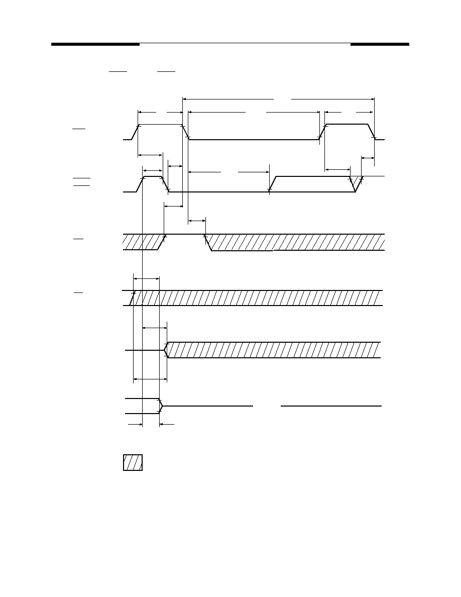
MOSEL VITELIC
V53C518160A
Waveforms of RAS Only Refresh Cycle
Row
Row
HI-Z
Address
RAS
I/O
(Outputs)
"H" or "L"
V
IH
V
IL
V
IH
V
IL
V
IH
V
IL
V
OH
V
OL
t
RC
t
RAS
t
RP
t
CRP
t
RPC
t
ASR
t
ASR
t
RAH
UCAS
LCAS
511816502-14
20
V53C518160A Rev. 1.3 March 1998
MOSEL VITELIC
V53C518160A
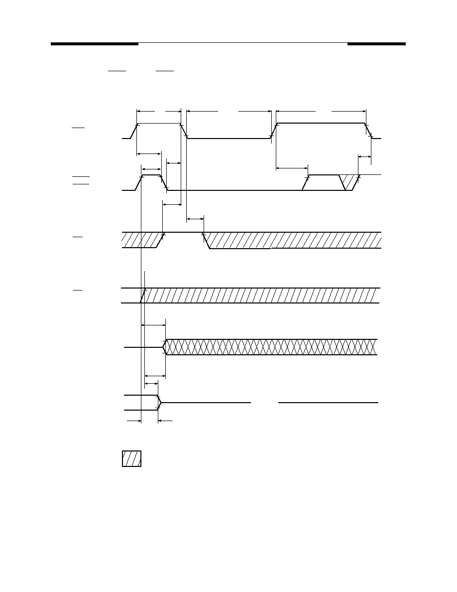
Waveforms of CAS-before-RAS Refresh Cycle
t
RC
HI-Z
"H" or "L"
RAS
I/O
(Outputs)
I/O
(Inputs)
OE
WE
V
IH
V
IL
V
IH
V
IL
V
IH
V
IL
V
IH
V
IL
V
IH
V
IL
V
OH
V
OL
t
RAS
t
RP
t
RP
t
RPC
t
CSR
t
CP
t
CHR
t
RPC
t
CRP
t
WRP
t
WRH
t
OEZ
t
CDD
t
ODD
t
OFF
UCAS
LCAS
511816502-15
21
V53C518160A Rev. 1.3 March 1998
MOSEL VITELIC
V53C518160A
Waveforms of CAS-before-RAS Self Refresh Cycle (Optional)
HI-Z
"H" or "L"
RAS
I/O
(Outputs)
I/O
(Inputs)
OE
WE
V
IH
V
IL
V
IH
V
IL
V
IH
V
IL
V
IH
V
IL
V
IH
V
IL
V
OH
V
OL
t
RASS
t
RPS
t
RP
t
RPC
t
CSR
t
CP
t
CHS
t
CRP
t
WRP
t
WRH
t
OEZ
t
CDD
t
ODD
t
OFF
UCAS
LCAS
511816502-15

22
V53C518160A Rev. 1.3 March 1998
MOSEL VITELIC
V53C518160A
Waveforms of Hidden Refresh Read Cycle
RAS
I/O
(Outputs)
I/O
(Inputs)
OE
WE
Address
"H" or "L"
Valid Data Out
Row
Column
Row
HI-Z
511816502-16
V
IH
V
IL
V
IH
V
IL
V
IH
V
IL
V
IH
V
IL
V
IH
V
IL
V
IH
V
IL
V
OH
V
OL
t
RC
t
RC
t
RAS
t
RP
t
RAS
t
RP
t
RCD
t
RSH
t
CHR
t
CRP
t
RAD
t
ASC
t
RAH
t
ASR
t
CAH
t
WRP
t
WRH
t
ASR
t
RRH
t
RCS
t
CAA
t
OAC
t
DZC
t
DZO
t
CDD
t
ODD
t
OFF
t
OEZ
t
CAC
t
CLZ
t
RAC
UCAS
LCAS

23
V53C518160A Rev. 1.3 March 1998
MOSEL VITELIC
V53C518160A
Waveforms of Hidden Refresh Early Write Cycle
RAS
I/O
(Output)
I/O
(Input)
WE
Address
"H" or "L"
t
RC
Row
Row
Valid Data
HI-Z
Column
V
IH
V
IL
V
IH
V
IL
V
IH
V
IL
V
IH
V
IL
V
IH
V
IL
V
OH
V
OL
t
RAS
t
RP
t
RCD
t
RSH
t
RC
t
RAS
t
RP
t
CRP
t
CHR
t
RAD
t
RAH
t
ASR
t
ASC
t
CAH
t
ASR
t
WCS
t
WCH
t
WP
t
WRP
t
WRH
t
DS
t
DH
UCAS
LCAS
511816502-17

24
V53C518160A Rev. 1.3 March 1998
MOSEL VITELIC
V53C518160A
Functional Description
The V53C518160A is a CMOS dynamic RAM op-
timized for high data bandwidth, low power applica-
tions. It is functionally similar to a traditional
dynamic RAM. The V53C518160A reads and writes
data by multiplexing an 20-bit address into a 10-bit
row and a 10-bit column address. The row address
is latched by the Row Address Strobe (RAS). The
column address "flows through" an internal address
buffer and is latched by the Column Address Strobe
(CAS). Because access time is primarily dependent
on a valid column address rather than the precise
time that the CAS edge occurs, the delay time from
RAS to CAS has little effect on the access time.
Memory Cycle
A memory cycle is initiated by bringing RAS low.
Any memory cycle, once initiated, must not be end-
ed or aborted before the minimum t
RAS
time has ex-
pired. This ensures proper device operation and
data integrity. A new cycle must not be initiated until
the minimum precharge time t
RP
/t
CP
has elapsed.
Read Cycle
A Read cycle is performed by holding the Write
Enable (WE) signal High during a RAS/CAS opera-
tion. The column address must be held for a mini-
mum specified by t
AR
. Data Out becomes valid only
when t
OAC
, t
RAC
, t
CAA
and t
CAC
are all satisifed. As
a result, the access time is dependent on the timing
relationships between these parameters. For exam-
ple, the access time is limited by t
CAA
when t
RAC
,
t
CAC
and t
OAC
are all satisfied.
Write Cycle
A Write Cycle is performed by taking WE and
CAS low during a RAS operation. The column ad-
dress is latched by CAS. The Write Cycle can be
WE controlled or CAS controlled depending on
whether WE or CAS falls later. Consequently, the
input data must be valid at or before the falling edge
of WE or CAS, whichever occurs last. In the CAS-
controlled Write Cycle, when the leading edge of
WE occurs prior to the CAS low transition, the I/O
data pins will be in the High-Z state at the beginning
of the Write function. Ending the Write with RAS or
CAS will maintain the output in the High-Z state.
In the WE controlled Write Cycle, OE must be in
the high state and t
OED
must be satisfied.
Fast Page Mode
Fast Page operation permits all 1024 columns
within a selected row of the device to be randomly
accessed at a high data rate. Maintaining RAS low
while performing successive CAS cycles retains the
row address internally and eliminates the need to
reapply it for each cycle. The column address buffer
acts as a transparent or flow-through latch while
CAS is high. Thus, access begins from the occur-
rence of a valid column address rather than from the
falling edge of CAS, eliminating t
ASC
and t
T
from the
critical timing path. CAS latches the address into the
column address buffer. During Fast Page operation,
Read, Write, Read-Modify-Write or Read-Write-
Read cycles are possible at random addresses
within a row. Following the initial entry cycle into
EDO Mode, access is t
CAA
or t
CAP
controlled. If the
column address is valid prior to the rising edge of
CAS, the access time is referenced to the CAS ris-
ing edge and is specified by t
CAP
. If the column ad-
dress is valid after the rising CAS edge, access is
timed from the occurrence of a valid address and is
specified by t
CAA
. In both cases, the falling edge of
CAS latches the address and enables the output.
Fast Page provides a sustained data rate of 29
MHz for applications that require high bandwidth
such as bit-mapped graphics or high-speed signal
processing. The following equation can be used to
calculate the maximum data rate:
Self Refresh
Self Refresh mode provides internal refresh con-
trol signals to the DRAM during extended periods of
inactivity. Device operation in this mode provides
additional power savings and design ease by elimi-
nation of external refresh control signals. Self Re-
fresh mode is initialed with a CAS before RAS
(CBR) Refresh cycle, holding both RAS low (t
RASS
)
and CAS low (t
CHD
) for a specified period. Both of
these parameters are specified with minimum val-
ues to guarantee entry into Self Refresh operation.
Once the device has been placed in to Self Refresh
mode the CAS clock is no longer required to main-
tain Self Refresh operation.
The Self Refresh mode is terminated by returning
the RAS clock to a high level for a specified (t
RPS
)
minimum time. After termination of the Self Refresh
cycle normal accesses to the device may be initiat-
ed immediately, poviding that subsequest refresh
cycles utilize the CAS before RAS (CBR) mode of
operation.
Data Rate
1024
t
RC
1023
t
PC
�
+
--------------------------------------------
=

MOSEL VITELIC
V53C518160A
25
V53C518160A Rev. 1.3 March 1998
Data Output Operation
The V53C518160A Input/Output is controlled by
OE, CAS, WE and RAS. A RAS low transition en-
ables the transfer of data to and from the selected
row address in the Memory Array. A RAS high tran-
sition disables data transfer and latches the output
data if the output is enabled. After a memory cycle
is initiated with a RAS low transition, a CAS low
transition or CAS low level enables the internal I/O
path. A CAS high transition or a CAS high level dis-
ables the I/O path and the output driver if it is en-
abled. A CAS low transition while RAS is high has
no effect on the I/O data path or on the output driv-
ers. The output drivers, when otherwise enabled,
can be disabled by holding OE high. The OE signal
has no effect on any data stored in the output latch-
es. A WE low level can also disable the output driv-
ers when CAS is low. During a Write cycle, if WE
goes low at a time in relationship to CAS that would
normally cause the outputs to be active, it is neces-
sary to use OE to disable the output drivers prior to
the WE low transition to allow Data In Setup Time
(t
DS
) to be satisfied.
Power-On
After application of the V
CC
supply, an initial
pause of 200
m
s is required followed by a minimum
of 8 initialization cycles (any combination of cycles
containing a RAS clock). Eight initialization cycles
are required after extended periods of bias without
clocks (greater than the Refresh Interval).
During Power-On, the V
CC
current requirement of
the V53C518160A is dependent on the input levels
of RAS and CAS. If RAS is low during Power-On,
the device will go into an active cycle and I
CC
will ex-
hibit current transients. It is recommended that RAS
and CAS track with V
CC
or be held at a valid V
IH
dur-
ing Power-On to avoid current surges.
Table 1. V53C518160A Data Output
Operation for Various Cycle Types
Cycle Type
I/O State
Read Cycles
Data from Addressed
Memory Cell
CAS-Controlled Write Cycle
(Early Write)
High-Z
WE-Controlled Write
Cycle (Late Write)
OE Controlled. High
OE = High-Z I/Os
Read-Modify-Write Cycles
Data from Addressed
Memory Cell
EDO Read Cycle
Data from Addressed
Memory Cell
EDO Write Cycle (Early Write)
High-Z
EDO Read-Modify-Write Cycle
Data from Addressed
Memory Cell
RAS-only Refresh
High-Z
CAS-before-RAS
Refresh Cycle
High-Z
CAS-only Cycles
High-Z

26
V53C518160A Rev. 1.3 March 1998
MOSEL VITELIC
V53C518160A
Notes:
27
V53C518160A Rev. 1.3 March 1998
MOSEL VITELIC
V53C518160A
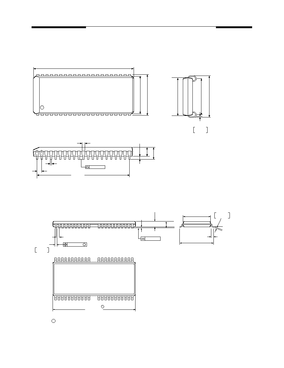
Package Diagrams
42-Pin 400 mil SOJ
44/50-Pin 400 mil TSOP-II
1.08
�0.010
[27.41
�0.25
]
0.05 [1.27]
1.0 [25.4]
0.017
�
0.004
[0.43
�
0.1]
0.004 [0.1]
0.045 [1.15] MIN
0.145 [3.68] MAX
.406
�0.012
[10.3
�0.3
]
.441
�
0.006
[11.2
�
0.15
]
42
1
22
21
0.370
�
0.010 [9.4
�
0.25]
.406
�0.012
(1)
[10.3 � 0.3]
.441
�0.006
[11.2
�0.15
]
(1)
0.2
Unit in inches [mm]
0.81 [.032] MAX
+0.12
�0.05
0.008
+0.005
�0.002
0.088
�
0.004
[2.24
�
0.1]
(1) Does not include plastic or metal protrusion of 0.010 [0.25] max per side.
50
26
36
40
1
25
15
11
0.016
+0.002
�0.004
0.4
+0.05
�0.1
0.006
+0.003
�0.001
0.15
+0.08
�0.03
0.008 [0.2]
44x
M
Unit in inches [mm]
0.004
�
0.002
[0.1
�
0.05]
0.031 [0.8]
0.039
�
0.002
[1
�
0.05]
0.4
�
0.005
[10.16
�
0.13]
0.463
�
0.008
[11.76
�
0.2]
0.047 Max
[1.2 Max]
0.004 [0.1]
0.825
�
0.005
[20.95
�
0.13]
Does not include plastic or metal protrusion of 0.010 [0.25] max. per side
1
1
0.020
�
0.004
[0.5
�
0.1]

MOSEL VITELIC
WORLDWIDE OFFICES
V53C518160A
� Copyright 1998, MOSEL VITELIC Inc.
3/98
Printed in U.S.A.
MOSEL VITELIC
3910 N. First Street, San Jose, CA 95134-1501 Ph: (408) 433-6000 Fax: (408) 433-0952 Tlx: 371-9461
U.S. SALES OFFICES
The information in this document is subject to change without
notice.
MOSEL VITELIC makes no commitment to update or keep cur-
rent the information contained in this document. No part of this
document may be copied or reproduced in any form or by any
means without the prior written consent of MOSEL-VITELIC.
MOSEL VITELIC subjects its products to normal quality control
sampling techniques which are intended to provide an assurance
of high quality products suitable for usual commercial applica-
tions. MOSEL VITELIC does not do testing appropriate to provide
100% product quality assurance and does not assume any liabil-
ity for consequential or incidental arising from any use of its prod-
ucts. If such products are to be used in applications in which
personal injury might occur from failure, purchaser must do its
own quality assurance testing appropriate to such applications.
U.S.A.
3910 NORTH FIRST STREET
SAN JOSE, CA 95134
PHONE: 408-433-6000
FAX: 408-433-0185
HONG KONG
19 DAI FU STREET
TAIPO INDUSTRIAL ESTATE
TAIPO, NT, HONG KONG
PHONE: 852-2665-4883
FAX: 852-2664-7535
TAIWAN
7F, NO. 102
MIN-CHUAN E. ROAD, SEC. 3
TAIPEI
PHONE: 886-2-2545-1213
FAX: 886-2-2545-1209
1 CREATION ROAD I
SCIENCE BASED IND. PARK
HSIN CHU, TAIWAN, R.O.C.
PHONE: 886-3-578-3344
FAX: 886-3-579-2838
JAPAN
WBG MARINE WEST 25F
6, NAKASE 2-CHOME
MIHAMA-KU, CHIBA-SHI
CHIBA 261-71
PHONE: 81-43-299-6000
FAX: 81-43-299-6555
IRELAND & UK
BLOCK A UNIT 2
BROOMFIELD BUSINESS PARK
MALAHIDE
CO. DUBLIN, IRELAND
PHONE: +353 1 8038020
FAX: +353 1 8038049
GERMANY
(CONTINENTAL
EUROPE & ISRAEL )
71083 HERRENBERG
BENZSTR. 32
GERMANY
PHONE: +49 7032 2796-0
FAX: +49 7032 2796 22
NORTHWESTERN
3910 NORTH FIRST STREET
SAN JOSE, CA 95134
PHONE: 408-433-6000
FAX: 408-433-0185
NORTHEASTERN
SUITE 436
20 TRAFALGAR SQUARE
NASHUA, NH 03063
PHONE: 603-889-4393
FAX: 603-889-9347
SOUTHWESTERN
SUITE 200
5150 E. PACIFIC COAST HWY.
LONG BEACH, CA 90804
PHONE: 562-498-3314
FAX: 562-597-2174
CENTRAL & SOUTHEASTERN
604 FIELDWOOD CIRCLE
RICHARDSON, TX 75081
PHONE: 972-690-1402
FAX: 972-690-0341