 | Электронный компонент: 2N6240 | Скачать:  PDF PDF  ZIP ZIP |
1
Motorola Thyristor Device Data
Silicon Controlled Rectifiers
Reverse Blocking Triode Thyristors
. . . PNPN devices designed for high volume consumer applications such as
temperature, light, and speed control; process and remote control, and warning
systems where reliability of operation is important.
╖
Passivated Surface for Reliability and Uniformity
╖
Power Rated at Economical Prices
╖
Practical Level Triggering and Holding Characteristics
╖
Flat, Rugged, Thermopad Construction for Low Thermal Resistance, High Heat
Dissipation and Durability
╖
Recommended Electrical Replacement for C106
MAXIMUM RATINGS
(TJ = 25
░
C unless otherwise noted.)
Rating
Symbol
Value
Unit
*Repetitive Peak Forward and Reverse Blocking Voltage(1)
(1/2 Sine Wave)
(RGK = 1000 ohms, TC = ¡40 to +110
░
C)
VDRM
or
VRRM
400
Volts
*Non¡repetitive Peak Reverse Blocking Voltage
(1/2 Sine Wave, RGK = 1000 ohms,
TC = ¡40
░
to +110
░
C)
VRSM
450
Volts
*Average On¡State Current
(TC = ¡40 to + 90
░
C)
(TC = +100
░
C)
IT(AV)
2.6
1.6
Amps
*Surge On¡State Current
(1/2 Sine Wave, 60 Hz, TC = +90
░
C)
(1/2 Sine Wave, 1.5 ms, TC = +90
░
C)
ITSM
25
35
Amps
Circuit Fusing
(t = 8.3 ms)
I2t
2.6
A2s
*Peak Gate Power
(Pulse Width = 10
╡
s, TC = 90
░
C)
PGM
0.5
Watts
*Indicates JEDEC Registered Data.
(continued)
1. VDRM and VRRM for all types can be applied on a continuous basis. Ratings apply for zero or negative gate voltage; however, positive gate
voltage shall not be applied concurrent with negative potential on the anode. Blocking voltages shall not be tested with a constant current
source such that the voltage ratings of the devices are exceeded.
Order this document
by 2N6240/D
MOTOROLA
SEMICONDUCTOR TECHNICAL DATA
⌐
Motorola, Inc. 1999
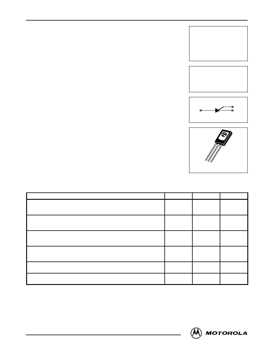
2N6240
CASE 77-08
(TO-225AA)
STYLE 2
SCRs
4 AMPERES RMS
400 VOLTS
K
A
G
A
K
A
G

2N6240
2
Motorola Thyristor Device Data
MAXIMUM RATINGS -- continued
(TJ = 25
░
C unless otherwise noted.)
Rating
Unit
Value
Symbol
*Average Gate Power
(t = 8.3 ms, TC = 90
░
C)
PG(AV)
0.1
Watt
Peak Forward Gate Current
IGM
0.2
Amp
Peak Reverse Gate Voltage
VRGM
6
Volts
*Operating Junction Temperature Range
TJ
¡40 to +110
░
C
*Storage Temperature Range
Tstg
¡40 to +150
░
C
Mounting Torque(1)
6
in. lb.
THERMAL CHARACTERISTICS
Characteristic
Symbol
Min
Max
Unit
*Thermal Resistance, Junction to Case
R
JC
--
3
░
C/W
Thermal Resistance, Junction to Ambient
R
JA
--
75
░
C/W
*Indicates JEDEC Registered Data.
ELECTRICAL CHARACTERISTICS
(TC = 25
░
C and RGK = 1000 ohms unless otherwise noted.)
Characteristic
Symbol
Min
Typ
Max
Unit
* Peak Forward or Reverse Blocking Current
(VAK = Rated VDRM or VRRM) TC = 25
░
C
TC = 110
░
C
IDRM, IRRM
--
--
--
--
10
200
╡
A
╡
A
*Peak Forward "On" Voltage
(ITM = 8.2 A Peak, Pulse Width = 1 to 2 ms, 2% Duty Cycle)
VTM
--
--
2.2
Volts
Gate Trigger Current (Continuous dc)(2)
(VAK = 12 Vdc, RL = 24 Ohms)
*(VAK = 12 Vdc, RL = 24 Ohms,
TC = ¡40
░
C)
IGT
--
--
--
--
200
500
╡
A
Gate Trigger Voltage (Continuous dc)
(Source Voltage = 12 V, RS = 50 Ohms)
*(VAK = 12 Vdc, RL = 24 Ohms, TC = ¡40
░
C)
VGT
--
--
1
Volts
Gate Non¡Trigger Voltage
(VAK = Rated VDRM, RL = 100 Ohms, TC = 110
░
C)
VGD
0.2
--
--
Volts
Holding Current
(VAK = 12 Vdc, IGT = 2 mA)
TC = 25
░
C
*(Initiating On¡State Current = 200 mA)
TC = ¡40
░
C
IH
--
--
--
--
5
10
mA
*Total Turn¡On Time
(Source Voltage = 12 V, RS = 6 k Ohms)
(ITM = 8.2 A, IGT = 2 mA, Rated VDRM)
(Rise Time = 20 ns, Pulse Width = 10
╡
s)
tgt
--
2
--
╡
s
Forward Voltage Application Rate
(VD = Rated VDRM, TC = 110
░
C)
dv/dt
--
10
--
V/
╡
s
*Indicates JEDEC Registered Data.
1. Torque rating applies with use of compression washer (B52200F006 or equivalent). Mounting torque in excess of 6 in. lb. does not appreciably
lower case-to-sink thermal resistance. Anode lead and heatsink contact pad are common. (See AN¡209 B)
For soldering purposes (either terminal connection or device mounting), soldering temperatures shall not exceed +200
░
C. For optimum
results an activated flux (oxide removing) is recommended.
2. Measurement does not include RGK current.

2N6240
3
Motorola Thyristor Device Data
dc
106
82
94
110
102
98
0
0.8
1.6
2.4
3.2
90
4.0
IT(AV), AVERAGE FORWARD CURRENT (AMP)
86
90
50
30
110
FIGURE 1 ¡ MAXIMUM CASE TEMPERATURE
0
FIGURE 2 ¡ MAXIMUM AMBIENT TEMPERATURE
IT(AV), AVERAGE FORWARD CURRENT (AMP)
0.1
0.2
0.3
0.4
180
░
90
░
60
░
= 30
░
dc
C
░
T
, MAXIMUM
ALLOW
ABLE CASE
TEMPERA
TURE ( C)
A
░
T
, MAXIMUM
ALLOW
ABLE
AMBIENT
0.4
1.2
2.0
2.8
3.6
0
f = 60 Hz
120
░
70
0.5
0.6
0.7
0.8
180
░
90
░
60
░
= 30
░
0
f = 60 Hz
TEMPERA
TURE ( C)

2N6240
4
Motorola Thyristor Device Data
PACKAGE DIMENSIONS
NOTES:
1. DIMENSIONING AND TOLERANCING PER ANSI
Y14.5M, 1982.
2. CONTROLLING DIMENSION: INCH.
STYLE 2:
PIN 1.
CATHODE
2.
ANODE
3.
GATE
¡B¡
¡A¡
M
K
F
C
Q
H
V
G
S
D
J
R
U
1
3
2
2 PL
M
A
M
0.25 (0.010)
B
M
M
A
M
0.25 (0.010)
B
M
DIM
MIN
MAX
MIN
MAX
MILLIMETERS
INCHES
A
0.425
0.435
10.80
11.04
B
0.295
0.305
7.50
7.74
C
0.095
0.105
2.42
2.66
D
0.020
0.026
0.51
0.66
F
0.115
0.130
2.93
3.30
G
0.094 BSC
2.39 BSC
H
0.050
0.095
1.27
2.41
J
0.015
0.025
0.39
0.63
K
0.575
0.655
14.61
16.63
M
5 TYP
5 TYP
Q
0.148
0.158
3.76
4.01
R
0.045
0.055
1.15
1.39
S
0.025
0.035
0.64
0.88
U
0.145
0.155
3.69
3.93
V
0.040
¡¡¡
1.02
¡¡¡
_
_
CASE 77¡08
(TO¡225AA)
Motorola reserves the right to make changes without further notice to any products herein. Motorola makes no warranty, representation or guarantee regarding
the suitability of its products for any particular purpose, nor does Motorola assume any liability arising out of the application or use of any product or circuit, and
specifically disclaims any and all liability, including without limitation consequential or incidental damages. "Typical" parameters which may be provided in Motorola
data sheets and/or specifications can and do vary in different applications and actual performance may vary over time. All operating parameters, including "Typicals"
must be validated for each customer application by customer's technical experts. Motorola does not convey any license under its patent rights nor the rights of
others. Motorola products are not designed, intended, or authorized for use as components in systems intended for surgical implant into the body, or other
applications intended to support or sustain life, or for any other application in which the failure of the Motorola product could create a situation where personal injury
or death may occur. Should Buyer purchase or use Motorola products for any such unintended or unauthorized application, Buyer shall indemnify and hold Motorola
and its officers, employees, subsidiaries, affiliates, and distributors harmless against all claims, costs, damages, and expenses, and reasonable attorney fees
arising out of, directly or indirectly, any claim of personal injury or death associated with such unintended or unauthorized use, even if such claim alleges that
Motorola was negligent regarding the design or manufacture of the part. Motorola and are registered trademarks of Motorola, Inc. Motorola, Inc. is an Equal
Opportunity/Affirmative Action Employer.
Mfax is a trademark of Motorola, Inc.
How to reach us:
USA / EUROPE / Locations Not Listed: Motorola Literature Distribution;
JAPAN: Motorola Japan Ltd.; SPD, Strategic Planning Office, 141,
P.O. Box 5405, Denver, Colorado 80217. 1¡303¡675¡2140 or 1¡800¡441¡2447
4¡32¡1 Nishi¡Gotanda, Shinagawa¡ku, Tokyo, Japan. 81¡3¡5487¡8488
Customer Focus Center: 1¡800¡521¡6274
Mfax
TM
: RMFAX0@email.sps.mot.com ¡ TOUCHTONE 1¡602¡244¡6609
ASIA/PACIFIC: Motorola Semiconductors H.K. Ltd.; Silicon Harbour Centre,
Motorola Fax Back System
¡ US & Canada ONLY 1¡800¡774¡1848
2, Dai King Street, Tai Po Industrial Estate, Tai Po, N.T., Hong Kong.
¡ http://sps.motorola.com/mfax/
852¡26629298
HOME PAGE: http://motorola.com/sps/
2N6240/D