 | –≠–ª–µ–∫—Ç—Ä–æ–Ω–Ω—ã–π –∫–æ–º–ø–æ–Ω–µ–Ω—Ç: BUT11AF | –°–∫–∞—á–∞—Ç—å:  PDF PDF  ZIP ZIP |

1
Motorola Bipolar Power Transistor Device Data
Full Pak
High Voltage NPN Power Transistor
For Isolated Package Applications
The BUT11AF was designed for use in line operated switching power supplies in a
wide range of end use applications. This device combines the latest state of the art
bipolar fabrication techniques to provide excellent switching, high voltage capability
and low saturation voltage.
∑
1000 Volt VCES Rating
∑
Low Base Drive Requirements
∑
Isolated Overmold Package
∑
Improved System Efficiency
∑
No Isolating Washers Required
∑
Reduced System Cost
∑
High Isolation Voltage Capability (4500 VRMS)
MAXIMUM RATINGS
Rating
Symbol
Value
Unit
Collector≠Emitter Sustaining Voltage
VCEO(sus)
450
Vdc
Collector≠Emitter Breakdown Voltage
VCES
1000
Vdc
Emitter≠Base Voltage
VEBO
9.0
Vdc
RMS Isolation Voltage (For 1 sec,
Per Figure 7
VISOL1
4500
TA = 25
∞
C, Rel. Humidity < 30%)
Per Figure 8
VISOL2
3500
V
Per Figure 9
VISOL3
2500
Collector Current -- Continuous
Collector Current
-- Pulsed (1)
IC
ICM
5.0
10
Adc
Base Current -- Continuous
Base Current
-- Pulsed (1)
IB
IBM
2.0
4.0
Adc
Total Power Dissipation @ TC = 25
∞
C*
Derated above 25
∞
C
PD
40
0.32
Watts
W/
∞
C
Operating and Storage Temperature Range
TJ, Tstg
≠ 65 to +150
∞
C
THERMAL CHARACTERISTICS
Thermal Resistance -- Junction to Case*
R
JC
3.125
∞
C/W
Maximum Lead Temperature for soldering purposes
1/8
from case for 5 sec.
TL
260
∞
C
(1) Pulse Test: Pulse Width = 5.0 ms, Duty Cycle
10%.
* Measurement made with thermocouple contacting the bottom insulated mounting surface of the package (in a location beneath the die),
the device mounted on a heatsink, thermal grease applied, and a mounting torque of 6 to 8 in . lbs.
Full Pak is a registered trademark of Motorola Inc.
MOTOROLA
SEMICONDUCTOR TECHNICAL DATA
Order this document
by BUT11AF/D
©
Motorola, Inc. 1995
BUT11AF
POWER TRANSISTOR
5.0 AMPERES
450 VOLTS
40 WATTS
CASE 221D≠02
TO≠220 TYPE
REV 2

BUT11AF
2
Motorola Bipolar Power Transistor Device Data
ELECTRICAL CHARACTERISTICS
(TC = 25
∞
C unless otherwise noted)
Characteristic
Symbol
Min
Typ
Max
Unit
OFF CHARACTERISTICS (1)
Collector-Emitter Sustaining Voltage (Figures 1 & 2)
(IC = 100 mAdc, IB = 0, L = 25
µ
H)
VCEO(sus)
450
≠
≠
Vdc
Collector Cutoff Current
(VCE = 1000 Vdc, VBE = 0)
(VCE = 1000 Vdc, VBE = 0, TJ = 125
∞
C)
ICES
≠
≠
≠
≠
1.0
2.0
mAdc
Emitter-Base Leakage
(VEB = 9.0 Vdc, IC = 0)
IEBO
≠
≠
10
mAdc
ON CHARACTERISTICS (1)
Collector-Emitter Saturation Voltage
(IC = 2.5 Adc, IB = 0.5 Adc)
VCE(sat)
≠
≠
1.5
Vdc
Base-Emitter Saturation Voltage
(IC = 2.5 Adc, IB = 0.5 Adc)
VBE(sat)
≠
≠
1.5
Vdc
DC Current Gain
(IC = 5.0 mAdc, VCE = 5.0 Vdc)
hFE
10
≠
≠
≠
≠
≠
DYNAMIC CHARACTERISTICS
Insulation Capacitance (Collector to External Heatsink)
Cc-hs
≠
15
≠
pF
SWITCHING CHARACTERISTICS
Inductive Load (Figures 3 & 4)
Storage
IC = 2.5 Adc, IB1 = 0.5 Adc
TJ = 25
∞
C
ts
≠
1100
1400
ns
Fall Time
IC = 2.5 Adc, IB1 = 0.5 Adc
TJ = 25
∞
C
tfi
≠
80
150
Storage
IC = 2.5 Adc, IB1 = 0.5 Adc
TJ = 100
∞
C
ts
≠
1200
1500
Fall Time
TJ = 100
∞
C
tfi
≠
140
300
Resistive Load (Figures 5 & 6)
Turn-On Time
IC = 2.5 Adc, IB1 = IB2 = 0.5 Adc
ton
≠
≠
1000
ns
Storage Time
IC = 2.5 Adc, IB1 = IB2 = 0.5 Adc
ts
≠
≠
4000
Fall Time
tf
≠
≠
800
(1) Pulse Test: Pulse Width = 300
µ
s
, Duty Cycle
2.0%.
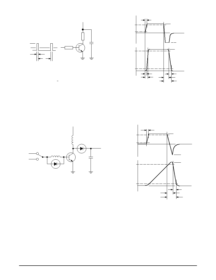
0
200
250
100
MIN
VCEO(sus)
VCE (V)
Figure 1. Oscilloscope Display for Sustaining Voltage
IC
(mA)
HOR.
OSCILLOSCOPE
VERT.
OSCILLOSCOPE
+50 V
L
VIN
0
tp
T
100 ≠ 200
1
Figure 2. Test Circuit for VCEO(sus)
BUT11AF
3
Motorola Bipolar Power Transistor Device Data
VIN
0
tp
T
RB
RL
T.U.T.
VCC
Figure 3. Test Circuit Resistive Load
VCC
VIN
tp
tp
T
= 250 V
= ≠ 6 to +8 V
= 20
µ
s
= 0.01
90%
10%
90%
10%
IB
IC
IB on
IB off
IC on
tr
t
td
ton
toff
ts
tf
t
Figure 4. Switching Times Waveforms with
Resistive Load
Figure 5. Test Circuit Inductive Load
+IB1
≠VBE
LB
VCC
LC
VCL
T.U.T.
7Z89211.2
VCL
VCC
VEB
LB
VCL
= 300 V
= 30 V
= 5 V
= 1
µ
H
= 200
µ
H
Figure 6. Switching Times Waveforms
with Inductive Load
90%
10%
90%
10%
IB
IC
IB1
IB2
IC on
tr
tf
ts
toff
t
BUT11AF
4
Motorola Bipolar Power Transistor Device Data
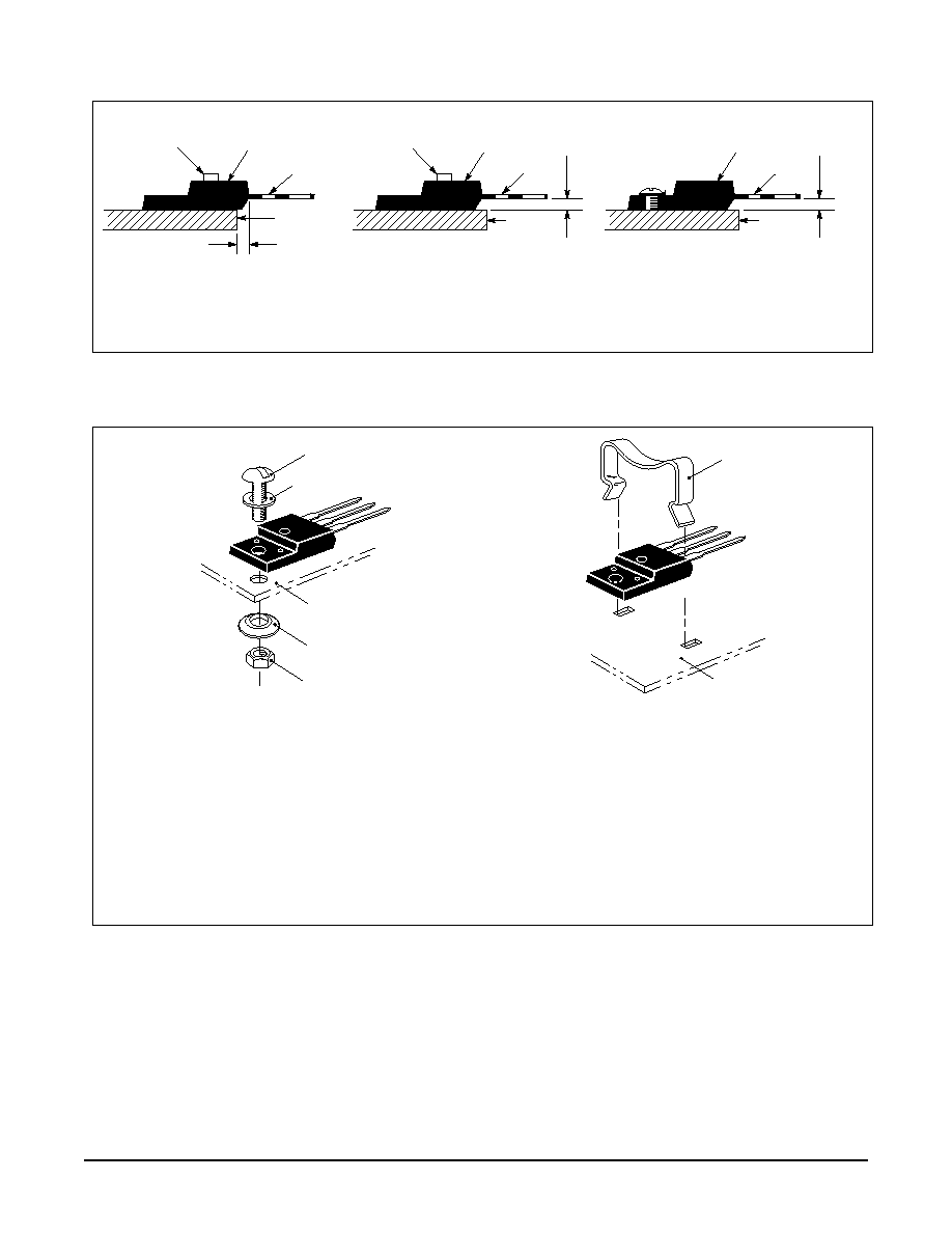
TEST CONDITIONS FOR ISOLATION TESTS*
MOUNTED
FULLY ISOLATED
PACKAGE
LEADS
HEATSINK
0.110
MIN
Figure 7. Screw or Clip Mounting Position
for Isolation Test Number 1
* Measurement made between leads and heatsink with all leads shorted together.
CLIP
MOUNTED
FULLY ISOLATED
PACKAGE
LEADS
HEATSINK
CLIP
0.107
MIN
MOUNTED
FULLY ISOLATED
PACKAGE
LEADS
HEATSINK
0.107
MIN
Figure 8. Clip Mounting Position
for Isolation Test Number 2
Figure 9. Screw Mounting Position
for Isolation Test Number 3
MOUNTING INFORMATION
4≠40 SCREW
PLAIN WASHER
HEATSINK
COMPRESSION WASHER
NUT
CLIP
HEATSINK
Laboratory tests on a limited number of samples indicate, when using the screw and compression washer mounting technique, a screw
torque of 6 to 8 in . lbs is sufficient to provide maximum power dissipation capability. The compression washer helps to maintain a constant
pressure on the package over time and during large temperature excursions.
Destructive laboratory tests show that using a hex head 4≠40 screw, without washers, and applying a torque in excess of 20 in . lbs will
cause the plastic to crack around the mounting hole, resulting in a loss of isolation capability.
Additional tests on slotted 4≠40 screws indicate that the screw slot fails between 15 to 20 in . lbs without adversely affecting the package.
However, in order to positively ensure the package integrity of the fully isolated device, Motorola does not recommend exceeding 10 in . lbs
of mounting torque under any mounting conditions.
Figure 10. Typical Mounting Techniques
for Isolated Package
BUT11AF
5
Motorola Bipolar Power Transistor Device Data
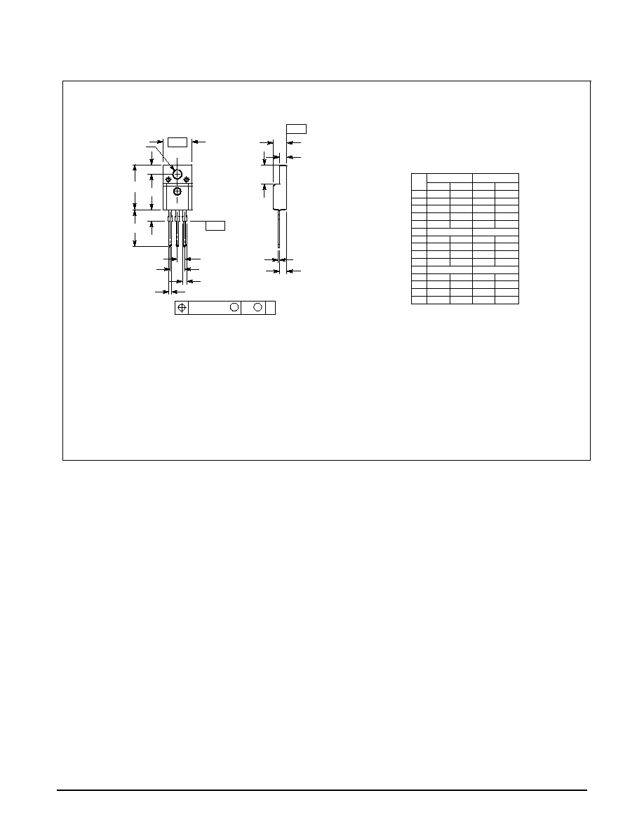
PACKAGE DIMENSIONS
CASE 221D≠02
TO≠220 TYPE
ISSUE D
NOTES:
1. DIMENSIONING AND TOLERANCING PER ANSI
Y14.5M, 1982.
2. CONTROLLING DIMENSION: INCH.
STYLE 2:
PIN 1. BASE
2. COLLECTOR
3. EMITTER
DIM
A
MIN
MAX
MIN
MAX
MILLIMETERS
0.621
0.629
15.78
15.97
INCHES
B
0.394
0.402
10.01
10.21
C
0.181
0.189
4.60
4.80
D
0.026
0.034
0.67
0.86
F
0.121
0.129
3.08
3.27
G
0.100 BSC
2.54 BSC
H
0.123
0.129
3.13
3.27
J
0.018
0.025
0.46
0.64
K
0.500
0.562
12.70
14.27
L
0.045
0.060
1.14
1.52
N
0.200 BSC
5.08 BSC
Q
0.126
0.134
3.21
3.40
R
0.107
0.111
2.72
2.81
S
0.096
0.104
2.44
2.64
U
0.259
0.267
6.58
6.78
≠B≠
≠Y≠
G
N
D
L
K
H
A
F
Q
3 PL
1 2 3
M
B
M
0.25 (0.010)
Y
SEATING
PLANE
≠T≠
U
C
S
J
R