 | –≠–ª–µ–∫—Ç—Ä–æ–Ω–Ω—ã–π –∫–æ–º–ø–æ–Ω–µ–Ω—Ç: MAC4DHM | –°–∫–∞—á–∞—Ç—å:  PDF PDF  ZIP ZIP |
1
Motorola Thyristor Device Data
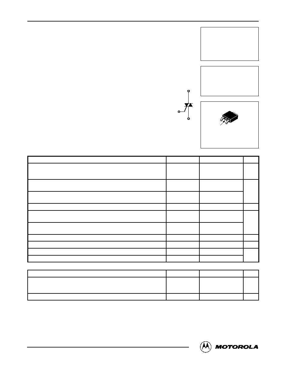
Sensitive Gate TRIACS
Silicon Bidirectional Thyristors
Designed for high volume, low cost, industrial and consumer applications
such as motor control; process control; temperature, light and speed control.
∑
Small Size Surface Mount DPAK Package
∑
Passivated Die for Reliability and Uniformity
∑
Four≠Quadrant Triggering
∑
Blocking Voltage to 600 V
∑
On≠State Current Rating of 4.0 Amperes RMS at 93
∞
C
∑
Low Level Triggering and Holding Characteristics
ORDERING INFORMATION
∑
To Obtain "DPAK" in Surface Mount Leadform (Case 369A)
Shipped in Sleeves -- No Suffix, i.e. MAC4DHM
Shipped in 16 mm Tape and Reel -- Add "T4" Suffix to Device Number,
i.e. MAC4DHMT4
∑
To Obtain "DPAK" in Straight Lead Version (Case 369) Shipped in Sleeves --
Add "≠1" Suffix to Device Number, i.e. MAC4DHM≠1
MAXIMUM RATINGS
(TJ = 25
∞
C unless otherwise noted)
Rating
Symbol
Value
Unit
Peak Repetitive Off≠State Voltage (1)
(TJ = ≠40 to 110
∞
C, Sine Wave, 50 to 60 Hz, Gate Open)
MAC4DHM
MAC4DLM
VDRM
600
600
Volts
On≠State RMS Current
(Full Cycle Sine Wave, 60 Hz, TC = 93
∞
C)
IT(RMS)
4.0
Amps
Peak Non≠Repetitive Surge Current
(One Full Cycle, 60 Hz, TJ = 110
∞
C)
ITSM
40
Circuit Fusing Consideration (t = 8.3 msec)
I2t
6.6
A2sec
Peak Gate Power
(Pulse Width
10
m
sec, TC = 93
∞
C)
PGM
0.5
Watts
Average Gate Power
(t = 8.3 msec, TC = 93
∞
C)
PG(AV)
0.1
Peak Gate Current (Pulse Width
10
m
sec, TC = 93
∞
C)
IGM
0.2
Amps
Peak Gate Voltage (Pulse Width
10
m
sec, TC = 93
∞
C)
VGM
5.0
Volts
Operating Junction Temperature Range
TJ
≠40 to 110
∞
C
Storage Temperature Range
Tstg
≠40 to 150
THERMAL CHARACTERISTICS
Characteristic
Symbol
Max
Unit
Thermal Resistance -- Junction to Case
Thermal Resistance
-- Junction to Ambient
Thermal Resistance
-- Junction to Ambient (2)
R
q
JC
R
q
JA
R
q
JA
3.5
88
80
∞
C/W
Maximum Lead Temperature for Soldering Purposes (3)
TL
260
∞
C
(1) VDRM for all types can be applied on a continuous basis. Ratings apply for zero or negative gate voltage; positive gate voltage shall not be
applied concurrent with negative potential on the anode. Blocking voltages shall not be tested with a constant current source such that the
voltage ratings of the device are exceeded.
(2) Surface mounted on minimum recommended pad size.
(3) 1/8
from case for 10 seconds.
Preferred devices are Motorola recommended choices for future use and best overall value.
Order this document
by MAC4DHM/D
MOTOROLA
SEMICONDUCTOR TECHNICAL DATA
MAC4DHM
MAC4DLM
TRIACS
4.0 AMPERES RMS
600 VOLTS
CASE 369A≠13
STYLE 6
MT2
MT1
G
MT2
G
MT2
MT1
Motorola Preferred Devices
©
Motorola, Inc. 1997

MAC4DHM MAC4DLM
2
Motorola Thyristor Device Data
ELECTRICAL CHARACTERISTICS
(TJ = 25
∞
C unless otherwise noted)
Characteristics
Symbol
Min
Typ
Max
Unit
Peak Repetitive Blocking Current
(VD = Rated VDRM, Gate Open)
TJ = 25
∞
C
TJ = 110
∞
C
IDRM
--
--
--
--
0.01
2.0
mA
Peak On≠State Voltage (1)
(ITM =
±
6.0 A)
VTM
--
1.3
1.6
Volts
Gate Trigger Current (Continuous dc) (VD = 12 V, RL = 100
W
)
MT2(+), G(+)
MAC4DLM
MT2(+), G(≠)
MT2(≠), G(≠)
MT2(≠), G(+)
MT2(+), G(+)
MAC4DHM
MT2(+), G(≠)
MT2(≠), G(≠)
MT2(≠), G(+)
IGT
--
--
--
--
--
--
--
--
1.8
2.1
2.4
4.2
1.8
2.1
2.4
4.2
3.0
3.0
3.0
5.0
5.0
5.0
5.0
10
mA
Gate Trigger Voltage (Continuous dc) (VD = 12 V, RL = 100
W
)
MT2(+), G(+)
MT2(+), G(≠)
MT2(≠), G(≠)
MT2(≠), G(+)
(VD = 12 V, RL = 10 K
W
, TJ = 110
∞
C)
MT2(+), G(+); MT2(+), G(≠); MT2(≠), G(≠); MT2(≠), G(+)
VGT
0.5
0.5
0.5
0.5
0.1
0.62
0.57
0.65
0.74
0.4
1.3
1.3
1.3
1.3
--
Volts
Holding Current
(VD = 12 V, Gate Open, IT =
±
200 mA)
IH
--
1.5
15
mA
Latching Current
MT2(+), G(+)
(VD = 12 V, IG = 5.0 mA)
MT2(+), G(≠)
(VD = 12 V, IG = 5.0 mA)
MT2(≠), G(≠)
(VD = 12 V, IG = 5.0 mA)
MT2(≠), G(+)
(VD = 12 V, IG = 10 mA)
IL
--
--
--
--
1.75
5.2
2.1
2.2
10
10
10
10
mA
DYNAMIC CHARACTERISTICS
Characteristics
Symbol
Min
Typ
Max
Unit
Rate of Change of Commutating Current (1)
(VD = 200 V, ITM = 1.8 A, Commutating dv/dt = 1.0 V/
m
sec, TJ = 110
∞
C,
f = 250 Hz, CL = 5.0
m
fd, LL = 80 mH, RS = 56
W
, CS = 0.03
m
fd)
See Figure 10
di/dt(c)
--
3.0
--
A/ms
Critical Rate of Rise of Off≠State Voltage
(VD = 0.67 X Rated VDRM, Exponential Waveform,
Gate Open, TJ = 110
∞
C)
dv/dt
--
10
--
V/
m
s
(1) Pulse test: Pulse Width
2.0 msec, Duty Cycle
2%.
MAC4DHM MAC4DLM
3
Motorola Thyristor Device Data
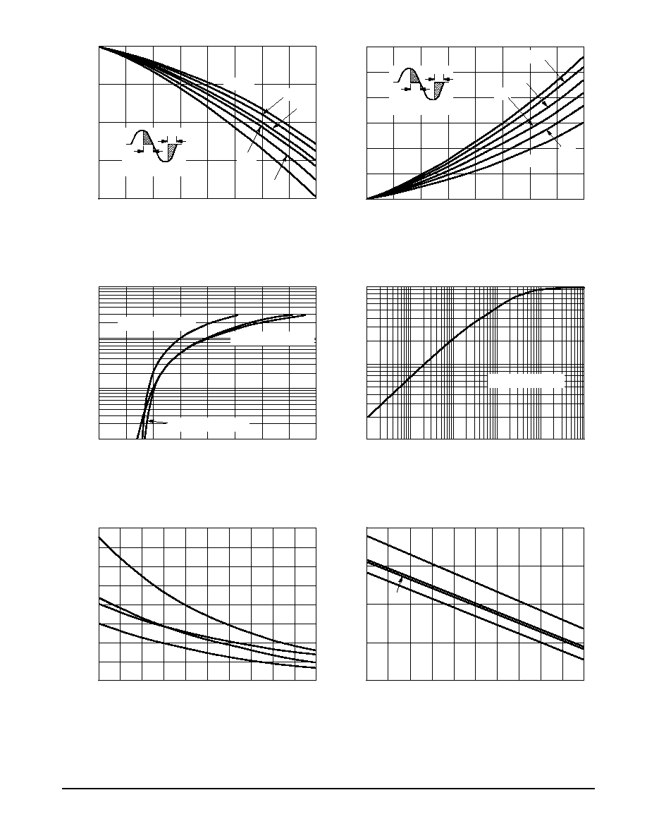
Figure 1. RMS Current Derating
Figure 2. On≠State Power Dissipation
Figure 3. On≠State Characteristics
Figure 4. Transient Thermal Response
Figure 5. Typical Gate Trigger Current versus
Junction Temperature
Figure 6. Typical Gate Trigger Voltage versus
Junction Temperature
2.5
4.0
0
IT(RMS), RMS ON≠STATE CURRENT (AMPS)
110
105
100
IT(RMS), RMS ON≠STATE CURRENT (AMPS)
3.0
4.0
0
4.0
2.0
1.0
0
4.0
0
VT, INSTANTANEOUS ON≠STATE VOLTAGE (VOLTS)
100
10
1.0
0.1
t, TIME (ms)
1.0
0.1
1.0
0.1
0.01
3.5
≠25
20
≠40
TJ, JUNCTION TEMPERATURE (
∞
C)
8.0
3.0
2.0
0
TJ, JUNCTION TEMPERATURE (
∞
C)
≠25
65
≠40
0.8
0.6
0.2
20
5.0
T C
, MAXIMUM
ALLOW
ABLE CASE
TEMPERA
TURE ( C)
P
I
r (t)
, TRANSIENT
RESIST
ANCE
(NORMALIZED)
95
90
0.5
1.0
1.5
2.0
3.0
3.5
1.0
2.0
3.0
5.0
6.0
1.0
0.5
3.0
10
100
1000
10 K
, GA
TE
TRIGGER
CURRENT
(mA)
I GT
50
110
65
4.0
5.0
110
35
50
0.4
V
GT
, GA
TE
TRIGGER
VOL
T
AGE
(VOL
TS)
∞
,
A
VERAGE POWER DISSIP
A
TION
(W
A
TTS)
(A
V)
, INST
ANT
ANEOUS
ON≠ST
A
TE
CURRENT
(AMPS)
T
80
5.0
dc
180
∞
120
∞
90
∞
60
∞
a
= 30
∞
dc
180
∞
120
∞
90
∞
60
∞
TYPICAL @ TJ = 25
∞
C
MAXIMUM @ TJ = 25
∞
C
MAXIMUM @ TJ = 110
∞
C
Z
q
JC(t) = R
q
JC(t)
S
r(t)
Q3
Q2
Q1
Q3
Q2
Q1
a
= CONDUCTION ANGLE
a
= CONDUCTION ANGLE
a
= 30
∞
1.0
1.0
2.5
3.5
0.5
1.5
2.5
2.0
1.5
≠10
35
95
6.0
7.0
Q4
≠10
95
80
Q4

MAC4DHM MAC4DLM
4
Motorola Thyristor Device Data
Figure 7. Typical Holding Current versus
Junction Temperature
Figure 8. Typical Latching Current versus
Junction Temperature
Figure 9. Exponential Static dv/dt versus
Gate≠MT1 Resistance, MT2(+)
65
110
≠40
TJ, JUNCTION TEMPERATURE (
∞
C)
2.0
TJ, JUNCTION TEMPERATURE (
∞
C)
20
110
≠40
4.0
2.0
0
1000
10 K
100
RGK, GATE≠MT1 RESISTANCE (OHMS)
20
15
10
5.0
0
I H
, HOLDING CURRENT
(mA)
I
ST
A
TIC dv/dt (V/ s)
1.0
0
≠25
5.0
20
50
95
≠25
5.0
8.0
10
12
, LA
TCHING
CURRENT
(mA)
L
4.0
3.0
5.0
80
50
65
m
MT2 POSITIVE
MT2 NEGATIVE
Q2
Q3
Q1
VD = 400 V
TJ = 110
∞
C
MT2 POSITIVE
6.0
≠10
35
80
≠10
35
95
Q4
Figure 10. Critical Rate of Rise of
Commutating Voltage
1.0
0
di/dt(c), RATE OF CHANGE OF COMMUTATING CURRENT (A/ms)
10
1.0
0.1
COMMUT
A
TING VOL
T
AGE (V/ s)
m
2.0
3.0
VPK = 400 V
100
∞
C
90
∞
C
TJ = 110
∞
C
tw
VDRM
(di/dt)c =
6f ITM
1000
f =
1
2 tw
dv/dt(c),
CRITICAL
RA
TE OF RISE OF
4.0
5.0
6.0
MT2 NEGATIVE
MAC4DHM MAC4DLM
5
Motorola Thyristor Device Data
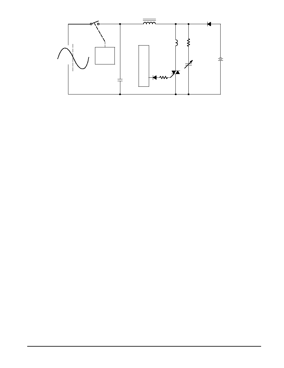
Figure 11. Simplified Test Circuit to Measure the Critical Rate of Rise of Commutating Voltage
80 mHY
LL
1N4007
200 V
+
MEASURE
I
≠
CHARGE
CONTROL
CHARGE
TRIGGER
5
m
F
NON-POLAR
CL
51
2
1
1N914
G
TRIGGER CONTROL
200 VRMS
ADJUST FOR
ITM, 60 Hz VAC
Note: Component values are for verification of rated (dv/dt)c. See AN1048 for additional information.
RS
56
W
0.03
m
F
ADJUST FOR
dv/dt(c)
CS