 | –≠–ª–µ–∫—Ç—Ä–æ–Ω–Ω—ã–π –∫–æ–º–ø–æ–Ω–µ–Ω—Ç: MC100EL14 | –°–∫–∞—á–∞—Ç—å:  PDF PDF  ZIP ZIP |
MOTOROLA
SEMICONDUCTOR TECHNICAL DATA
4≠1
REV 1
©
Motorola, Inc. 1996
7/95
1:5 Clock Distribution Chip
The MC100LVEL/100EL14 is a low skew 1:5 clock distribution chip
designed explicitly for low skew clock distribution applications. The
device can be driven by either a differential or single-ended ECL or, if
positive power supplies are used, PECL input signal. The LVEL14 is
functionally and pin compatible with the EL14 but is designed to operate
in ECL or PECL mode for a voltage supply range of ≠3.0V to ≠3.8V ( or
3.0V to 3.8V). If a single-ended input is to be used the VBB output should
be connected to the CLK input and bypassed to ground via a 0.01
µ
F
capacitor. The VBB output is designed to act as the switching reference
for the input of the LVEL14 under single-ended input conditions, as a
result this pin can only source/sink up to 0.5mA of current.
The LVEL14 features a multiplexed clock input to allow for the
distribution of a lower speed scan or test clock along with the high speed
system clock. When LOW (or left open and pulled LOW by the input
pulldown resistor) the SEL pin will select the differential clock input.
The common enable (EN) is synchronous so that the outputs will only
be enabled/disabled when they are already in the LOW state. This avoids
any chance of generating a runt clock pulse when the device is
enabled/disabled as can happen with an asynchronous control. The
internal flip flop is clocked on the falling edge of the input clock, therefore
all associated specification limits are referenced to the negative edge of
the clock input.
∑
50ps Output-to-Output Skew
∑
Synchronous Enable/Disable
∑
Multiplexed Clock Input
∑
75k
Internal Input Pulldown Resistors
∑
>2000V ESD Protection
∑
VEE Range of ≠3.0V to ≠5.5V
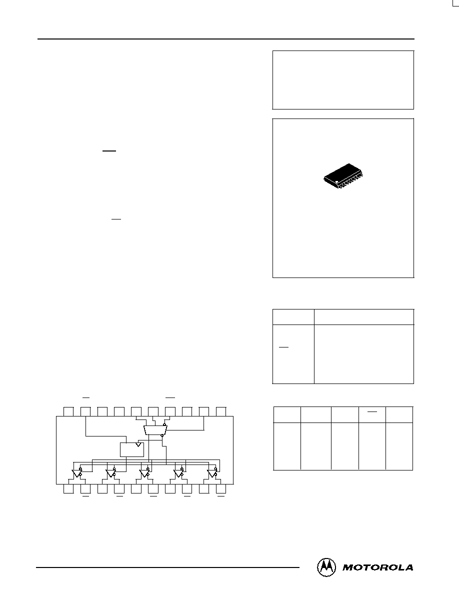
LOGIC DIAGRAM AND PINOUT ASSIGNMENT
Q1
Q2
Q3
Q4
17
18
16
15
14
13
12
4
3
5
6
7
8
9
VCC
11
10
Q4
Q3
Q2
Q1
NC
SCLK
CLK
CLK
VBB
SEL
VEE
D
Q
1 0
Q0
19
20
2
1
VCC
Q0
EN
MC100LVEL14
MC100EL14
DW SUFFIX
PLASTIC SOIC PACKAGE
CASE 751D-04
1
20
PIN
FUNCTION
CLK
Diff Clock Inputs
SCLK
Scan Clock Input
EN
Sync Enable
SEL
Clock Select Input
VBB
Reference Output
Q0≠4
Diff Clock Outputs
PIN DESCRIPTION
CLK
L
H
X
X
X
SCLK
X
X
L
H
X
SEL
L
L
H
H
X
EN
L
L
L
L
H
Q
L
H
L
H
L*
FUNCTION TABLE
* On next negative transition of
CLK or SCLK

MC100LVEL14 MC100EL14
MOTOROLA
ECLinPS and ECLinPS Lite
DL140 -- Rev 3
4≠2
ABSOLUTE MAXIMUM RATINGS1
Symbol
Characteristic
Rating
Unit
VEE
Power Supply (VCC = 0V)
≠8.0 to 0
VDC
VI
Input Voltage (VCC = 0V)
0 to ≠6.0
VDC
Iout
Output Current
Continuous
Surge
50
100
mA
TA
Operating Temperature Range
≠40 to +85
∞
C
VEE
Operating Range1,2
≠5.7 to ≠4.2
V
1. Absolute maximum rating, beyond which, device life may be impaired, unless otherwise specified on an individual data sheet.
2. Parametric values specified at:
100EL Series:
≠4.20V to ≠5.50V
10EL Series:
≠4.94V to ≠5.50V
DC CHARACTERISTICS (VEE = VEE(min) ≠ VEE(max); VCC = GND1)
≠40
∞
C
0
∞
C to 85
∞
C
Symbol
Characteristic
Min
Typ
Max
Min
Typ
Max
Unit
Condition
VOH
Output HIGH Voltage
≠1085
≠1005
≠880
≠1025
≠955
≠880
mV
VIN = VIH(max)
VOL
Output LOW Voltage
≠1830
≠1695
≠1555
≠1810
≠1705
≠1620
mV
or VIL(min)
VOHA
Output HIGH Voltage
≠1095
--
--
≠1035
--
--
mV
VIN = VIH(max)
VOLA
Output LOW Voltage
--
--
≠1555
--
--
≠1610
mV
or VIL(min)
VIH
Input HIGH Voltage
≠1165
--
≠880
≠1165
--
≠880
mV
VIL
Input LOW Voltage
≠1810
--
≠1475
≠1810
--
≠1475
mV
IIL
Input LOW Current
CLK
Others
≠300
0.5
--
--
≠300
0.5
--
--
µ
A
VIN = VIL(max)
1. This table replaces the three tables traditionally seen in ECL 100K data books. The same DC parameter values at VEE = ≠4.5V now apply across
the full VEE range of ≠3.0V to ≠5.5V. Outputs are terminated through a 50
resistor to ≠2.0V except where otherwise specified on the individual
data sheets.
MC100LVEL14 MC100EL14
4≠3
MOTOROLA
ECLinPS and ECLinPS Lite
DL140 -- Rev 3
MC100LVEL14 AC/DC CHARACTERISTICS (VEE = ≠3.8V to ≠3.0V; VCC = GND)
≠40
∞
C
0
∞
C
25
∞
C
85
∞
C
Symbol
Characteristic
Min
Typ
Max
Min
Typ
Max
Min
Typ
Max
Min
Typ
Max
Unit
IEE
Power Supply Current
100LVEL
100EL
32
32
40
40
32
32
40
40
32
32
40
40
34
34
42
42
mA
VBB
Output Ref
100LVEL
Voltage
100EL
≠1.43
≠1.38
≠1.30
≠1.26
≠1.38
≠1.38
≠1.27
≠1.26
≠1.35
≠1.38
≠1.25
≠1.26
≠1.31
≠1.38
≠1.19
≠1.26
V
IIH
Input High Current
150
150
150
150
µ
tPLH
tPHL
Prop
CLK to Q (Diff)
Delay
CLK to Q (SE)
SCLK to Q
520
470
470
720
770
770
550
500
500
750
800
800
580
530
530
680
680
680
780
830
830
630
580
580
830
880
880
ps
tSKEW
Part-to-Part Skew
Within-Device Skew1
200
50
200
50
200
50
200
50
ps
tS
Setup Time EN
0
0
0
0
ps
tH
Hold Time EN
0
0
0
0
ps
VPP
Minimum Input Swing CLK
150
150
150
150
mV
VCMR
Common Mode Range2
VPP < 500mV
VPP
500mV
≠2.0
≠1.8
≠0.4
≠0.4
≠2.1
≠1.9
≠0.4
≠0.4
≠2.1
≠1.9
≠0.4
≠0.4
≠2.1
≠1.9
≠0.4
≠0.4
V
tr
tf
Output Rise/Fall Times Q
(20% ≠ 80%)
230
500
230
500
230
500
230
500
ps
1. Skews are specified for identical LOW-to-HIGH or HIGH-to-LOW transitions.
2. The CMR range is referenced to the most positive side of the differential input signal. Normal operation is obtained if the HIGH level falls within
the specified range and the peak-to-peak voltage lies between VPPmin and 1V. The lower end of the CMR range varies 1:1 with VEE. The
numbers in the spec table assume a nominal VEE = ≠3.3V. Note for PECL operation, the VCMR(min) will be fixed at 3.3V ≠ |VCMR(min)|.
MC100EL14 AC/DC CHARACTERISTICS (VEE = ≠4.2V to ≠5.5V; VCC = GND)
≠40
∞
C
0
∞
C
25
∞
C
85
∞
C
Symbol
Characteristic
Min
Typ
Max
Min
Typ
Max
Min
Typ
Max
Min
Typ
Max
Unit
IEE
Power Supply Current
100LVEL
100EL
32
32
40
40
32
32
40
40
32
32
40
40
34
34
42
42
mA
VBB
Output Ref
100LVEL
Voltage
100EL
≠1.43
≠1.38
≠1.30
≠1.26
≠1.38
≠1.38
≠1.27
≠1.26
≠1.35
≠1.38
≠1.25
≠1.26
≠1.31
≠1.38
≠1.19
≠1.26
V
IIH
Input High Current
150
150
150
150
µ
tPLH
tPHL
Prop
CLK to Q (Diff)
Delay
CLK to Q (SE)
SCLK to Q
520
470
470
720
770
770
550
500
500
750
800
800
580
530
530
680
680
680
780
830
830
630
580
580
830
880
880
ps
tSKEW
Part-to-Part Skew
Within-Device Skew1
200
50
200
50
200
50
200
50
ps
tS
Setup Time EN
0
0
0
0
ps
tH
Hold Time EN
0
0
0
0
ps
VPP
Minimum Input Swing CLK
150
150
150
150
mV
VCMR
Common Mode Range2
VPP < 500mV
VPP
500mV
≠3.2
≠3.0
≠0.4
≠0.4
≠3.3
≠3.1
≠0.4
≠0.4
≠3.3
≠3.1
≠0.4
≠0.4
≠3.3
≠3.1
≠0.4
≠0.4
V
tr
tf
Output Rise/Fall Times Q
(20% ≠ 80%)
230
500
230
500
230
500
230
500
ps
1. Skews are specified for identical LOW-to-HIGH or HIGH-to-LOW transitions.
2. The CMR range is referenced to the most positive side of the differential input signal. Normal operation is obtained if the HIGH level falls within
the specified range and the peak-to-peak voltage lies between VPPmin and 1V. The lower end of the CMR range varies 1:1 with VEE. The
numbers in the spec table assume a nominal VEE = ≠4.5V. Note for PECL operation, the VCMR(min) will be fixed at 5.0V ≠ |VCMR(min)|.

MC100LVEL14 MC100EL14
MOTOROLA
ECLinPS and ECLinPS Lite
DL140 -- Rev 3
4≠4
OUTLINE DIMENSIONS
D SUFFIX
PLASTIC SOIC PACKAGE
CASE 751D-04
ISSUE E
MIN
MIN
MAX
MAX
MILLIMETERS
INCHES
DIM
A
B
C
D
F
G
J
K
M
P
R
0.510
0.299
0.104
0.019
0.035
0.012
0.009
7
∞
0.415
0.029
0.499
0.292
0.093
0.014
0.020
0.010
0.004
0
∞
0.395
0.010
12.95
7.60
2.65
0.49
0.90
0.32
0.25
7
∞
10.55
0.75
12.65
7.40
2.35
0.35
0.50
0.25
0.10
0
∞
10.05
0.25
NOTES:
1. DIMENSIONING AND TOLERANCING PER
ANSI Y14.5M, 1982.
2. CONTROLLING DIMENSION: MILLIMETER.
3. DIMENSIONS A AND B DO NOT INCLUDE
MOLD PROTRUSION.
4. MAXIMUM MOLD PROTRUSION 0.150
(0.006) PER SIDE.
5. DIMENSION D DOES NOT INCLUDE
DAMBAR PROTRUSION. ALLOWABLE
DAMBAR PROTRUSION SHALL BE 0.13
(0.005) TOTAL IN EXCESS OF D DIMENSION
AT MAXIMUM MATERIAL CONDITION.
1.27 BSC
0.050 BSC
-A-
-B-
P
10 PL
1
10
11
20
-T-
D
20 PL
K
C
SEATING
PLANE
R
X 45
∞
M
0.010 (0.25)
B
M
M
0.010 (0.25)
T
A
B
M
S
S
G
18 PL
F
J
Motorola reserves the right to make changes without further notice to any products herein. Motorola makes no warranty, representation or guarantee regarding
the suitability of its products for any particular purpose, nor does Motorola assume any liability arising out of the application or use of any product or circuit, and
specifically disclaims any and all liability, including without limitation consequential or incidental damages. "Typical" parameters which may be provided in Motorola
data sheets and/or specifications can and do vary in different applications and actual performance may vary over time. All operating parameters, including "Typicals"
must be validated for each customer application by customer's technical experts. Motorola does not convey any license under its patent rights nor the rights of
others. Motorola products are not designed, intended, or authorized for use as components in systems intended for surgical implant into the body, or other
applications intended to support or sustain life, or for any other application in which the failure of the Motorola product could create a situation where personal injury
or death may occur. Should Buyer purchase or use Motorola products for any such unintended or unauthorized application, Buyer shall indemnify and hold Motorola
and its officers, employees, subsidiaries, affiliates, and distributors harmless against all claims, costs, damages, and expenses, and reasonable attorney fees
arising out of, directly or indirectly, any claim of personal injury or death associated with such unintended or unauthorized use, even if such claim alleges that
Motorola was negligent regarding the design or manufacture of the part. Motorola and are registered trademarks of Motorola, Inc. Motorola, Inc. is an Equal
Opportunity/Affirmative Action Employer.
How to reach us:
USA/EUROPE/Locations Not Listed: Motorola Literature Distribution;
JAPAN: Nippon Motorola Ltd.; Tatsumi≠SPD≠JLDC, 6F Seibu≠Butsuryu≠Center,
P.O. Box 20912; Phoenix, Arizona 85036. 1≠800≠441≠2447 or 602≠303≠5454
3≠14≠2 Tatsumi Koto≠Ku, Tokyo 135, Japan. 03≠81≠3521≠8315
MFAX: RMFAX0@email.sps.mot.com ≠ TOUCHTONE 602≠244≠6609
ASIA/PACIFIC: Motorola Semiconductors H.K. Ltd.; 8B Tai Ping Industrial Park,
INTERNET: http://Design≠NET.com
51 Ting Kok Road, Tai Po, N.T., Hong Kong. 852≠26629298
MC100LVEL14/D
*MC100LVEL14/D*