MOTOROLA
SEMICONDUCTOR TECHNICAL DATA
3≠1
REV 2
©
Motorola, Inc. 1996
12/93
˜
2,
˜
4,
˜
8 Clock
Generation Chip
The MC10/100EL34 is a low skew
˜
2,
˜
4,
˜
8 clock generation chip
designed explicitly for low skew clock generation applications. The
internal dividers are synchronous to each other, therefore, the common
output edges are all precisely aligned. The device can be driven by either
a differential or single-ended ECL or, if positive power supplies are used,
PECL input signal. In addition, by using the VBB output, a sinusoidal
source can be AC coupled into the device (see Interfacing section of the
ECLinPS
TM
Data Book DL140/D). If a single-ended input is to be used, the
VBB output should be connected to the CLK input and bypassed to ground
via a 0.01
µ
F capacitor. The VBB output is designed to act as the switching
reference for the input of the EL34 under single-ended input conditions,
as a result, this pin can only source/sink up to 0.5mA of current.
The common enable (EN) is synchronous so that the internal dividers
will only be enabled/disabled when the internal clock is already in the
LOW state. This avoids any chance of generating a runt clock pulse on
the internal clock when the device is enabled/disabled as can happen
with an asynchronous control. An internal runt pulse could lead to losing
synchronization between the internal divider stages. The internal enable
flip-flop is clocked on the falling edge of the input clock, therefore, all
associated specification limits are referenced to the negative edge of the
clock input.
Upon startup, the internal flip-flops will attain a random state; the
master reset (MR) input allows for the synchronization of the internal
dividers, as well as multiple EL34s in a system.
∑
50ps Output-to-Output Skew
∑
Synchronous Enable/Disable
∑
Master Reset for Synchronization
∑
75k
Internal Input Pulldown Resistors
∑
>1000V ESD Protection
VCC
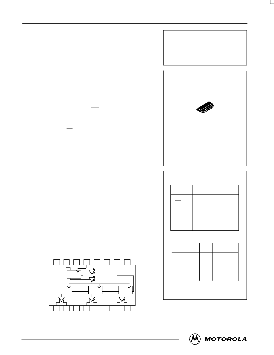
LOGIC DIAGRAM AND PINOUT ASSIGNMENT
Q0
Q1
VCC
Q2
15
16
14
13
12
11
10
2
1
3
4
5
6
7
VCC
9
8
Q2
Q0
EN
NC
CLK
CLK
VBB
MR
VEE
D
Q
R
Q
R
˜
2
Q
R
˜
4
Q
R
˜
8
Q1
MC10EL34
MC100EL34
PIN
FUNCTION
CLK
Diff Clock Inputs
EN
Sync Enable
MR
Master Reset
VBB
Reference Output
Q0
Diff
˜
2 Outputs
Q1
Diff
˜
4 Outputs
Q2
Diff
˜
8 Outputs
PIN DESCRIPTION
CLK
Z
ZZ
X
EN
L
H
X
MR
L
L
H
FUNCTION
Divide
Hold Q0≠3
Reset Q0≠3
FUNCTION TABLE
Z = Low-to-High Transition
ZZ = High-to-Low Transition
D SUFFIX
PLASTIC SOIC PACKAGE
CASE 751B-05
1
16

MC10EL34 MC100EL34
MOTOROLA
ECLinPS and ECLinPS Lite
DL140 -- Rev 3
3≠2
AC/DC CHARACTERISTICS (VEE = VEE(min) to VEE(max); VCC = GND)
≠40
∞
C
0
∞
C
25
∞
C
85
∞
C
Symbol
Characteristic
Min
Typ
Max
Min
Typ
Max
Min
Typ
Max
Min
Typ
Max
Unit
fMAX
Max Toggle Frequency
1100
1100
1100
1100
MHz
IEE
Power Supply
10EL
Current
100EL
39
39
39
39
39
39
39
42
mA
VBB
Output Reference
10EL
Voltage
100EL
≠1.43
≠1.38
≠1.30
≠1.26
≠1.38
≠1.38
≠1.27
≠1.26
≠1.35
≠1.38
≠1.25
≠1.26
≠1.31
≠1.38
≠1.19
≠1.26
V
IIH
Input High Current
150
150
150
150
µ
tPLH
tPHL
Propagation
CLK
Q0
Delay to
CLK
Q1,2
Output
MR
Q
960
900
750
1200
1140
1060
960
900
750
1200
1140
1060
960
900
750
1200
1140
1060
970
910
790
1210
1150
1090
ps
tSKEW
Within-Device Skew
100
100
100
100
ps
tS
Setup Time EN
400
400
400
400
ps
tH
Hold Time EN
250
250
250
250
ps
VPP
Minimum Input Swing
CLK
250
250
250
250
mV
VCMR
Common Mode Range
CLK
≠2.0
≠0.4
≠2.0
≠0.4
≠2.0
≠0.4
≠2.0
≠0.4
V
tr
tf
Output Rise/Fall Times Q
(20% ≠ 80%)
275
525
275
525
275
525
275
525
ps
Figure 1. Timing Diagram
CLK
Q0
Q1
Q2
EN
The EN signal will freeze the internal clocks to the flip≠flops on the first falling edge of CLK after its assertion. The internal dividers will maintain their state
during the internal clock freeze and will return to clocking once the internal clocks are unfrozen. The outputs will transition to their next states in the same
manner, time and relationship as they would have had the EN signal not been asserted.
Internal Clock
Disabled
Internal Clock
Enabled

MC10EL34 MC100EL34
3≠3
MOTOROLA
ECLinPS and ECLinPS Lite
DL140 -- Rev 3
OUTLINE DIMENSIONS
D SUFFIX
PLASTIC SOIC PACKAGE
CASE 751B-05
ISSUE J
NOTES:
1. DIMENSIONING AND TOLERANCING PER ANSI
Y14.5M, 1982.
2. CONTROLLING DIMENSION: MILLIMETER.
3. DIMENSIONS A AND B DO NOT INCLUDE
MOLD PROTRUSION.
4. MAXIMUM MOLD PROTRUSION 0.15 (0.006)
PER SIDE.
5. DIMENSION D DOES NOT INCLUDE DAMBAR
PROTRUSION. ALLOWABLE DAMBAR
PROTRUSION SHALL BE 0.127 (0.005) TOTAL
IN EXCESS OF THE D DIMENSION AT
MAXIMUM MATERIAL CONDITION.
1
8
16
9
SEATING
PLANE
F
J
M
R
X 45
_
G
8 PL
P
≠B≠
≠A≠
M
0.25 (0.010)
B
S
≠T≠
D
K
C
16 PL
S
B
M
0.25 (0.010)
A
S
T
DIM
MIN
MAX
MIN
MAX
INCHES
MILLIMETERS
A
9.80
10.00
0.386
0.393
B
3.80
4.00
0.150
0.157
C
1.35
1.75
0.054
0.068
D
0.35
0.49
0.014
0.019
F
0.40
1.25
0.016
0.049
G
1.27 BSC
0.050 BSC
J
0.19
0.25
0.008
0.009
K
0.10
0.25
0.004
0.009
M
0
7
0
7
P
5.80
6.20
0.229
0.244
R
0.25
0.50
0.010
0.019
_
_
_
_
Motorola reserves the right to make changes without further notice to any products herein. Motorola makes no warranty, representation or guarantee regarding
the suitability of its products for any particular purpose, nor does Motorola assume any liability arising out of the application or use of any product or circuit, and
specifically disclaims any and all liability, including without limitation consequential or incidental damages. "Typical" parameters which may be provided in Motorola
data sheets and/or specifications can and do vary in different applications and actual performance may vary over time. All operating parameters, including "Typicals"
must be validated for each customer application by customer's technical experts. Motorola does not convey any license under its patent rights nor the rights of
others. Motorola products are not designed, intended, or authorized for use as components in systems intended for surgical implant into the body, or other
applications intended to support or sustain life, or for any other application in which the failure of the Motorola product could create a situation where personal injury
or death may occur. Should Buyer purchase or use Motorola products for any such unintended or unauthorized application, Buyer shall indemnify and hold Motorola
and its officers, employees, subsidiaries, affiliates, and distributors harmless against all claims, costs, damages, and expenses, and reasonable attorney fees
arising out of, directly or indirectly, any claim of personal injury or death associated with such unintended or unauthorized use, even if such claim alleges that
Motorola was negligent regarding the design or manufacture of the part. Motorola and are registered trademarks of Motorola, Inc. Motorola, Inc. is an Equal
Opportunity/Affirmative Action Employer.
How to reach us:
USA/EUROPE/Locations Not Listed: Motorola Literature Distribution;
JAPAN: Nippon Motorola Ltd.; Tatsumi≠SPD≠JLDC, 6F Seibu≠Butsuryu≠Center,
P.O. Box 20912; Phoenix, Arizona 85036. 1≠800≠441≠2447 or 602≠303≠5454
3≠14≠2 Tatsumi Koto≠Ku, Tokyo 135, Japan. 03≠81≠3521≠8315
MFAX: RMFAX0@email.sps.mot.com ≠ TOUCHTONE 602≠244≠6609
ASIA/PACIFIC: Motorola Semiconductors H.K. Ltd.; 8B Tai Ping Industrial Park,
INTERNET: http://Design≠NET.com
51 Ting Kok Road, Tai Po, N.T., Hong Kong. 852≠26629298
MC10EL34/D
*MC10EL34/D*