
MOTOROLA
SEMICONDUCTOR TECHNICAL DATA
Order Number: MC100ES6254/D
Rev. 3, 05/2004
© Motorola, Inc. 2004
REV 3
2.5/3.3V Differential LVPECL
2x2 Clock Switch and
Fanout Buffer
The Motorola MC100ES6254 is a bipolar monolithic differential 2x2 clock
switch and fanout buffer. Designed for most demanding clock distribution sys-
tems, the MC100ES6254 supports various applications that require to drive pre-
cisely aligned clock signals. The device is capable of driving and switching dif-
ferential LVPECL signals. Using SiGe technology and a fully differential archi-
tecture, the device offers superior digital signal characteristics and very low
clock skew error. Target applications for this clock driver are high performance
clock/data switching, clock distribution or data loopback in computing, network-
ing and telecommunication systems.
Features:
∑ Fully differential architecture from input to all outputs
∑ SiGe technology supports near-zero output skew
∑ Supports DC to 3GHz operation
1
of clock or data signals
∑ LVPECL compatible differential clock inputs and outputs
∑ LVCMOS compatible control inputs
∑ Single 3.3 V or 2.5 V supply
∑ 50 ps maximum device skew
1
∑ Synchronous output enable eliminating output runt pulse generation and
metastability
∑ Standard 32 lead LQFP package
∑ Industrial temperature range
Functional Description
MC100ES6254 is designed for very skew critical differential clock distribution systems and supports clock frequencies from DC
up to 3.0 GHz. Typical applications for the MC100ES6254 are primary clock distribution, switching and loopback systems of
high-performance computer, networking and telecommunication systems, as well as on-board clocking of OC-3, OC-12 and OC-48
speed communication systems. Primary purpose of the MC100ES6254 is high-speed clock switching applications. In addition, the
MC100ES6254 can be configured as single 1:6 or dual 1:3 LVPECL fanout buffer for clock signals, or as loopback device in high-
speed data applications.
The MC100ES6254 can be operated from a 3.3 V or 2.5 V positive supply without the requirement of a negative supply line.
1
The device is functional up to 3 GHz and characterized up to 2.7 GHz.
FA SUFFIX
32-LEAD LQFP PACKAGE
CASE 873A
MC100ES6254
2.5/3.3 V DIFFERENTIAL
LVPECL 2x2
CLOCK SWITCH
AND FANOUT BUFFER
F
r
e
e
s
c
a
l
e
S
e
m
i
c
o
n
d
u
c
t
o
r
,
I
Freescale Semiconductor, Inc.
For More Information On This Product,
Go to: www.freescale.com
n
c
.
.
.

MC100ES6254/D
2
TIMING SOLUTIONS
QA0
QA0
QA1
QA2
QA2
QA1
OEB
QB0
QB0
QB1
QB2
QB2
QB1
CLK0
CLK0
SEL1
SEL0
V
CC
Bank A
Bank B
CLK1
CLK1
V
CC
OEA
0
1
0
1
Figure 1. MC100ES6254 Logic Diagram
Sync
QA2
VCC
QA1
QA0
QB2
VCC
QB1
VCC
VCC
GN
D
OE
A
CLK0
CLK0
SE
L
0
GN
D
VCC
VCC
GND
SE
L
1
CL
K
1
CL
K
1
OEB
GND
VCC
25
26
27
28
29
30
31
32
15
14
13
12
11
10
9
1
2
3
4
5
6
7
8
24
23
22
21
20
19
18
17
16
MC100ES6254
VCC
QB0
QB0
QB1
QB2
QA0
QA1
QA2
Figure 2. 32-Lead Package Pinout (Top View)
F
r
e
e
s
c
a
l
e
S
e
m
i
c
o
n
d
u
c
t
o
r
,
I
Freescale Semiconductor, Inc.
For More Information On This Product,
Go to: www.freescale.com
n
c
.
.
.
MC100ES6254/D
TIMING SOLUTIONS
3
a.
Absolute maximum continuous ratings are those maximum values beyond which damage to the device may occur. Exposure to these conditions
or conditions beyond those indicated may adversely affect device reliability. Functional operation at absolute-maximum-rated conditions is not
implied.
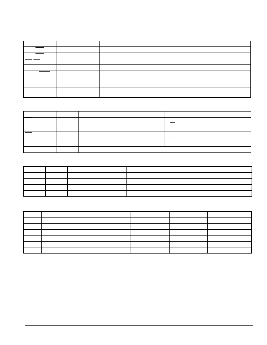
Table 1. PIN CONFIGURATION
Pin
I/O
Type
Function
CLK0, CLK0
Input
LVPECL
Differential reference clock signal input 0
CLK1, CLK1
Input
LVPECL
Differential reference clock signal input 1
OEA, OEB
Input
LVCMOS
Output enable
SEL0, SEL1
Input
LVCMOS
Clock switch select
QA[0-2], QA[0-2]
QB[0-2], QB[0-2]
Output
LVPECL
Differential clock outputs (banks A and B)
GND
Supply
GND
Negative power supply
V
CC
Supply
VCC
Positive power supply. All V
CC
pins must be connected to the positive power supply for correct
DC and AC operation
Table 2. FUNCTION TABLE
Control
Default
0
1
OEA
0
QA[0-2], Qx[0-2] are active. Deassertion of OE can be
asynchronous to the reference clock without generation
of output runt pulses
QA[0-2] = L, QA[0-2] = H (outputs disabled). Assertion
of OE can be asynchronous to the reference clock
without generation of output runt pulses
OEB
0
QA[0-2], Qx[0-2] are active. Deassertion of OE can be
asynchronous to the reference clock without generation
of output runt pulses
QA[0-2] = L, QA[0-2] = H (outputs disabled). Assertion
of OE can be asynchronous to the reference clock
without generation of output runt pulses
SEL0, SEL1
00
Refer to Table 3
Table 3. CLOCK SELECT CONTROL
SEL0
SEL1
CLK0 routed to
CLK1 routed to
Application Mode
0
0
QA[0:2] and QB[0:2]
---
1:6 fanout of CLK0
0
1
---
QA[0:2] and QB[0:2]
1:6 fanout of CLK1
1
0
QA[0:2]
QB[0:2]
Dual 1:3 buffer
1
1
QB[0:2]
QA[0:2]
Dual 1:3 buffer (crossed)
Table 4. ABSOLUTE MAXIMUM RATINGS
a
Symbol
Characteristics
Min
Max
Unit
Condition
V
CC
Supply Voltage
-0.3
3.6
V
V
IN
DC Input Voltage
-0.3
V
CC
+0.3
V
V
OUT
DC Output Voltage
-0.3
V
CC
+0.3
V
I
IN
DC Input Current
±20
mA
I
OUT
DC Output Current
±50
mA
T
S
Storage temperature
-65
125
∞C
F
r
e
e
s
c
a
l
e
S
e
m
i
c
o
n
d
u
c
t
o
r
,
I
Freescale Semiconductor, Inc.
For More Information On This Product,
Go to: www.freescale.com
n
c
.
.
.

MC100ES6254/D
4
TIMING SOLUTIONS
a.
Output termination voltage V
TT
=0 V for V
CC
=2.5 V operation is supported but the power consumption of the device will increase.
b.
Operating junction temperature impacts device life time. Maximum continuous operating junction temperature should be selected according to
the application life time requirements (See application note AN1545 and the application section in this data sheet for more information). The
device AC and DC parameters are specified up to 110
∞C junction temperature allowing the MC100ES6254 to be used in applications requiring
industrial temperature range. It is recommended that users of the MC100ES6254 employ thermal modeling analysis to assist in applying the
junction temperature specifications to their particular application.
a.
Input have internal pullup/pulldown resistors that affect the input current.
b.
V
PP
is the minimum differential input voltage swing required to maintain AC characteristic.
c.
V
CMR
(DC) is the crosspoint of the differential input signal. Functional operation is obtained when the crosspoint is within the V
CMR
(DC) range
and the input swing lies within the V
PP
(DC) specification.
d.
Equivalent to a termination 50
to V
TT
.
e.
I
CC
calculation:
I
CC
= (number of differential output pairs used) * (I
OH
+ I
OL
) + I
GND
I
CC
= (number of differential output pairs used) * (V
OH
-V
TT
)
˜
R
load
+(V
OL
-V
TT
)
˜
R
load
) + I
GND
Table 5. GENERAL SPECIFICATIONS
Symbol
Characteristics
Min
Typ
Max
Unit
Condition
V
TT
Output termination voltage
V
CC
- 2
a
V
MM
ESD Protection (Machine model)
200
V
HBM
ESD Protection (Human body model)
2000
V
CDM
ESD Protection (Charged device model)
1500
V
LU
Latch-up immunity
200
mA
C
IN
4.0
pF
Inputs
JA
Thermal resistance junction to ambient
JESD 51-3, single layer test board
JESD 51-6, 2S2P multilayer test board
83.1
73.3
68.9
63.8
57.4
59.0
54.4
52.5
50.4
47.8
86.0
75.4
70.9
65.3
59.6
60.6
55.7
53.8
51.5
48.8
∞C/W
∞C/W
∞C/W
∞C/W
∞C/W
∞C/W
∞C/W
∞C/W
∞C/W
∞C/W
Natural convection
100 ft/min
200 ft/min
400 ft/min
800 ft/min
Natural convection
100 ft/min
200 ft/min
400 ft/min
800 ft/min
JC
Thermal resistance junction to case
23.0
26.3
∞C/W
MIL-SPEC 883E Method 1012.1
Operating junction temperature
b
(continuous operation)
MTBF = 9.1 years
110
∞C
T
Func
Functional temperature range
T
A
=-40
T
J
=+110
∞C
Table 6. DC CHARACTERISTICS (V
CC
= 3.3 V
± 5% or 2.5 V ± 5%, T
J
= 0
∞ to +110∞C)
Symbol
Characteristics
Min
Typ
Max
Unit
Condition
LVCMOS control inputs (OEA, OEB, SEL0, SEL1)
V
IL
Input voltage low
0.8
V
V
IH
Input voltage high
2.0
V
I
IN
Input Currenta
±100
µA
V
IN
=V
CC
or V
IN
=GND
LVPECL clock inputs (CLK0, CLK0, CLK1, CLK1)
V
PP
AC differential input voltageb
0.1
1.3
V
Differential operation
V
CMR
Differential cross point voltagec
1.0
V
CC
-0.3
V
Differential operation
LVPECL clock outputs (QA0-2, QA0-2, QB0-2, QB0-2)
V
OH
Output High Voltage
V
CC
-1.2
V
CC
-1.005
V
CC
-0.7
V
I
OH
= -30 mA
d
V
OL
Output Low Voltage
V
CC
=3.3 V
±5%
V
CC
=2.5 V
±5%
V
CC
-1.9
V
CC
-1.9
V
CC
-1.705
V
CC
-1.705
V
CC
-1.5
V
CC
-1.3
V
I
OL
= -5 mA
e
I
GND
Maximum Quiescent Supply Current
without output termination current
52
85
mA
GND pin
F
r
e
e
s
c
a
l
e
S
e
m
i
c
o
n
d
u
c
t
o
r
,
I
Freescale Semiconductor, Inc.
For More Information On This Product,
Go to: www.freescale.com
n
c
.
.
.

MC100ES6254/D
TIMING SOLUTIONS
5
a.
AC characteristics apply for parallel output termination of 50
to V
TT
.
b.
V
PP
is the minimum differential input voltage swing required to maintain AC characteristics including tpd and device-to-device skew.
c.
V
CMR
(AC) is the crosspoint of the differential input signal. Normal AC operation is obtained when the crosspoint is within the V
CMR
(AC) range
and the input swing lies within the V
PP
(AC) specification. Violation of V
CMR
(AC) or V
PP
(AC) impacts the device propagation delay, device and
part-to-part skew.
d.
The MC100ES6254 is fully operational up to 3.0 GHz and is characterized up to 2.7 GHz.
e.
Output pulse skew is the absolute difference of the propagation delay times: | t
PLH
- t
PHL
|.
f.
Propagation delay OE deassertion to differential output disabled (differential low: true output low, complementary output high).
g.
Propagation delay OE assertion to output enabled (active).
Table 7. AC CHARACTERISTICS (V
CC
= 3.3 V
± 5% or 2.5 V ± 5%, T
J
= 0
∞ to +110∞C)
a
Symbol
Characteristics
Min
Typ
Max
Unit
Condition
V
PP
Differential input voltageb (peak-to-peak)
0.3
1.3
V
V
CMR
Differential input crosspoint voltage
c
1.2
V
CC
-0.3
V
V
O(P-P)
Differential output voltage (peak-to-peak)
f
O
< 1.1 GHz
f
O
< 2.5 GHz
f
O
< 3.0 GHz
0.45
0.35
0.20
0.7
0.55
0.35
V
V
V
f
CLK
Input Frequency
0
3000
d
MHz
t
PD
Propagation delay CLK, 1 to QA[] or QB[]
360
485
610
ps
Differential
t
sk(O)
Output-to-output skew
50
ps
Differential
t
sk(PP)
Output-to-output skew(part-to-part)
250
ps
Differential
t
SK(P)
DC
O
Output pulse skewe
Output duty cycle
t
REF
< 100 MHz
t
REF
< 800 MHz
49.4
45.2
60
50.6
54.8
ps
%
%
DC
fref
= 50%
DC
fref
= 50%
t
JIT(CC)
Output cycle-to-cycle jitter
RMS (1
)
1
ps
SEL0
SEL1
t
r
, t
f
Output Rise/Fall Time
0.05
300
ps
20% to 80%
t
PDLf
Output disable time
2.5
T + t
PD
3.5
T + t
PD
ns
T = CLK period
t
PLDg
Output enable time
3
T + t
PD
4
T + t
PD
ns
T = CLK period
t
PDL
(OEX to Qx[])
50%
t
PLD
(OEX to Qx[])
Outputs disabled
CLKX
CLKX
OEX
Qx[]
Qx[]
Figure 3. MC100ES6254 output disable/enable timing
Figure 4. MC100ES6254 AC test reference
Differential
Pulse Generator
Z = 50
R
T
= 50
Z
O
= 50
DUT
MC100ES62
V
TT
R
T
= 50
Z
O
= 50
V
TT
F
r
e
e
s
c
a
l
e
S
e
m
i
c
o
n
d
u
c
t
o
r
,
I
Freescale Semiconductor, Inc.
For More Information On This Product,
Go to: www.freescale.com
n
c
.
.
.