 | ╨н╨╗╨╡╨║╤В╤А╨╛╨╜╨╜╤Л╨╣ ╨║╨╛╨╝╨┐╨╛╨╜╨╡╨╜╤В: MC100H642 | ╨б╨║╨░╤З╨░╤В╤М:  PDF PDF  ZIP ZIP |
MOTOROLA
SEMICONDUCTOR TECHNICAL DATA
2н1
REV 4
й
Motorola, Inc. 1996
9/96
68030/040 PECL-TTL Clock Driver
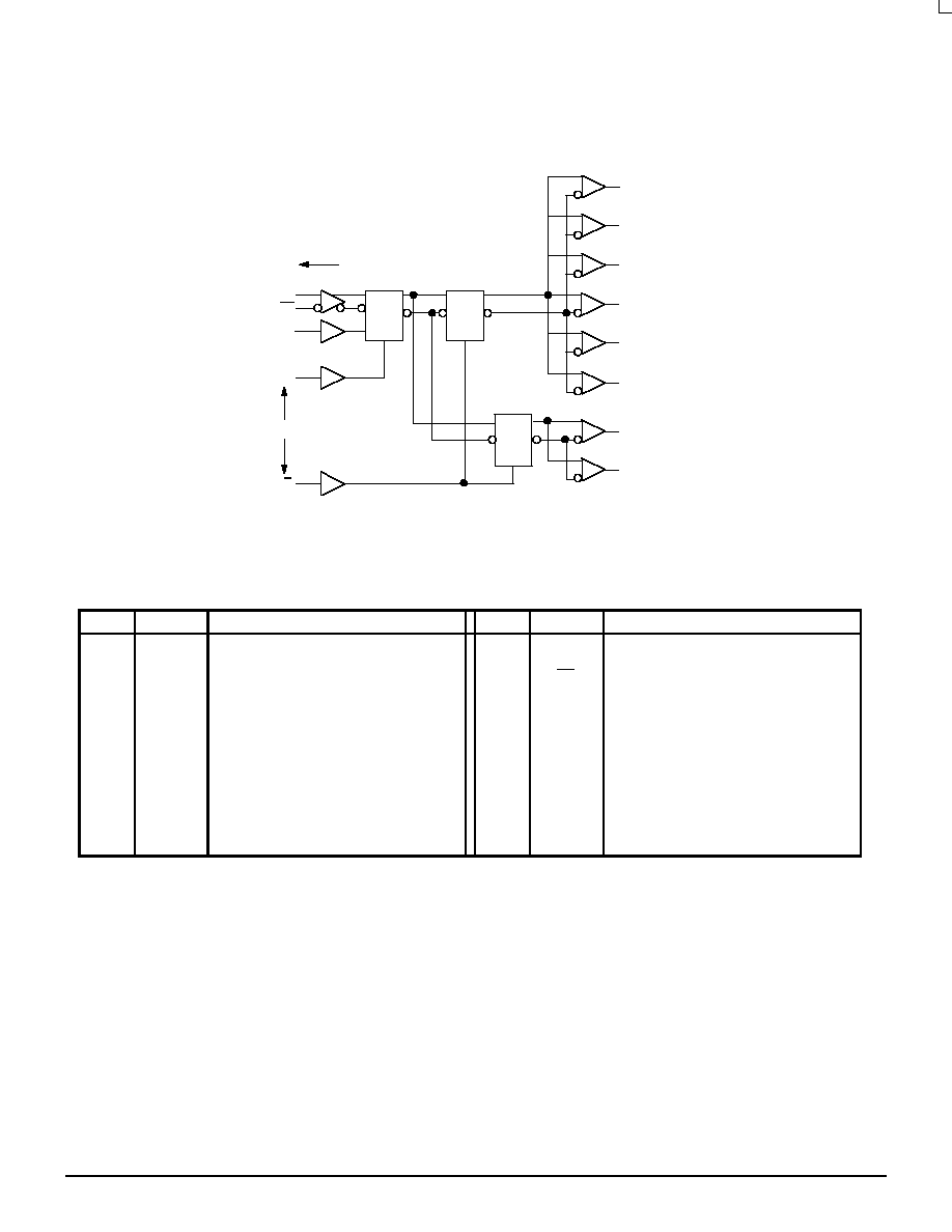
The MC10H/100H642 generates the necessary clocks for the 68030,
68040 and similar microprocessors. It is guaranteed to meet the clock
specifications required by the 68030 and 68040 in terms of partнtoнpart
skew, withinнpart skew and also duty cycle skew.
The user has a choice of using either TTL or PECL (ECL referenced to
+5.0V) for the input clock. TTL clocks are typically used in present MPU
systems. However, as clock speeds increase to 50MHz and beyond, the
inherent superiority of ECL (particularly differential ECL) as a means of
clock signal distribution becomes increasingly evident. The H642 also
uses differential PECL internally to achieve its superior skew
characteristic.
The H642 includes divideнbyнtwo and divideнbyнfour stages, both to
achieve the necessary duty cycle skew and to generate MPU clocks as
required. A typical 50MHz processor application would use an input clock
running at 100MHz, thus obtaining output clocks at 50MHz and 25MHz
(see Logic Diagram).
The 10H version is compatible with MECL 10H
TM
ECL logic levels,
while the 100H version is compatible with 100K levels (referenced to
+5.0V).
╖
Generates Clocks for 68030/040
╖
Meets 030/040 Skew Requirements
╖
TTL or PECL Input Clock
╖
Extra TTL and PECL Power/Ground Pins
╖
Asynchronous Reset
╖
Single +5.0V Supply
Function
Reset(R):
LOW on RESET forces all Q outputs LOW.
Select(SEL):
LOW selects the ECL input source (DE/DE).
HIGH selects the TTL input source (DT).
The H642 also contains circuitry to force a stable input state of the ECL differential input pair, should both sides be left open. In
this Case, the DE side of the input is pulled LOW, and DE goes HIGH.
Power Up:
The device is designed to have positive edges of the
і
2 and
і
4 outputs synchronized at Power Up.
1
VT
VT
Q1
GT
GT
Q0
VT
GT
GT
Q6
Q7
VT
SEL
5
6
7
8
9
10
11
25
24
23
22
21
20
19
Q5
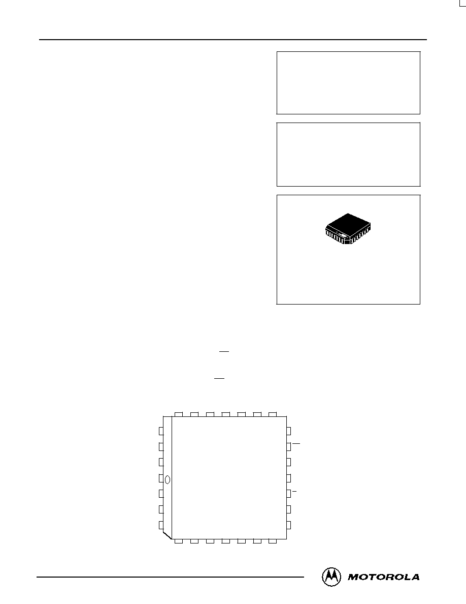
Pinout: 28нLead PLCC
(Top View)
VBB
DE
DE
VE
R
GE
DT
Q4
VT
VT
Q3
GT
GT
Q2
4
3
2
28
27
26
18
17
16
15
14
13
12
MC10H642
MC100H642
68030/040
PECLнTTL CLOCK
DRIVER
FN SUFFIX
PLASTIC PACKAGE
CASE 776н02
4
5
11
26
MC10H642 MC100H642
MOTOROLA
MECL Data
DL122 -- Rev 6
2н2
LOGIC DIAGRAM
TTL/ECL Clock Inputs
TTL Control Inputs
TTL Outputs
VBB
DE
DE
DT
SEL
R
і
4
і
2
MUX
Q7
Q6
Q5
Q4
Q3
Q2
Q1
Q0
PIN NAMES
Pin
Symbol
Description
Pin
Symbol
Description
8
1
8
2
8
3
8
4
8
5
8
6
8
7
8
8
8
9
10
11
12
13
14
Q3
VT
VT
Q4
Q5
GT
GT
Q6
Q7
VT
SEL
DT
GE
R
Signal Output (TTL)**
TTL VCC (+5.0V)
TTL VCC (+5.0V)
Signal Output (TTL)**
Signal Output (TTL)**
TTL Ground (0V)
TTL Ground (0V)
Signal Output (TTL)**
Signal Output (TTL)**
TTL VCC (+5.0V)
Input Select (TTL)
TTL Signal Input
ECL Ground (0V)
Reset (TTL)
15
16
17
18
19
20
21
22
23
24
25
26
27
28
VE
DE
DE
VBB
VT
Q0
GT
GT
Q1
VT
VT
Q2
GT
GT
ECL VCC (+5.0V)
ECL Signal Input (NonнInverting)
ECL Signal Input (Inverting)
VBB Reference Output
TTL VCC (+5.0V)
Signal Output (TTL)*
TTL Ground (0V)
TTL Ground (0V)
Signal Output (TTL)*
TTL VCC (+5.0V)
TTL VCC (+5.0V)
Signal Output (TTL)**
TTL Ground (0V)
TTL Ground (0V)
*
*Divide by 2
**Divide by 4
MC10H642 MC100H642
2н3
MOTOROLA
MECL Data
DL122 -- Rev 6
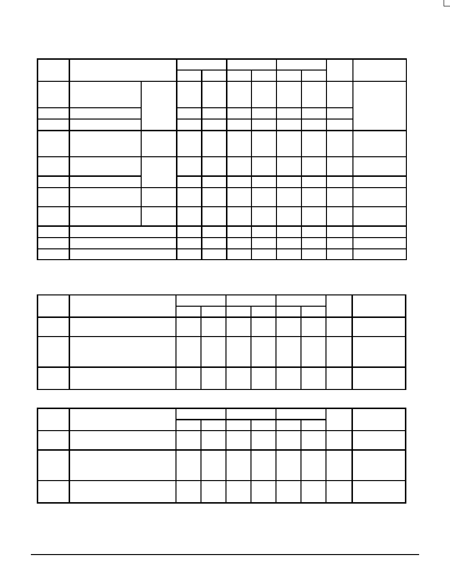
AC CHARACTERISTICS (VT = VE = 5.0V
▒
5%)
TA = 0
░
C
TA = 25
░
C
TA = 85
░
C
Symbol
Characteristic
Min
Max
Min
Max
Min
Max
Unit
Condition
tPLH
Propagation Delay
D to Output
Q2нQ7
C ECL
C TTL
4.70
4.70
5.70
5.70
4.75
4.75
5.75
5.75
4.60
4.50
5.60
5.50
ns
CL = 25pF
tskpp
PartнtoнPart Skew
1.0
1.0
1.0
ns
tskwd*
WithinнDevice Skew
0.5
0.5
0.5
ns
tPLH
Propagation Delay
D to Output
Q0, Q1
C ECL
C TTL
4.30
4.30
5.30
5.30
4.50
4.50
5.50
5.50
4.25
4.25
5.25
5.25
ns
CL = 25pF
tskpp
PartнtoнPart Skew
All
Outputs
2.0
2.0
2.0
ns
CL = 25pF
tskwd
WithinнDevice Skew
1.0
1.0
1.0
ns
CL = 25pF
tPD
Propagation Delay
R to Output
All
Outputs
4.3
6.3
4.0
6.0
4.5
6.5
ns
CL = 25pF
tR
tF
Output Rise/Fall Time
0.8 V to 2.0 V
All
Outputs
2.5
2.5
2.5
2.5
2.5
2.5
ns
CL = 25pF
fMAX**
Maximum Input Frequency
100
100
100
MHz
CL = 25pF
RPW
Reset Pulse Width
1.5
1.5
1.5
ns
RRT
Reset Recovery Time
1.25
1.25
1.25
ns
* WithinнDevice Skew defined as identical transactions on similar paths through a device.
** NOTE: MAX Frequency is 135MHz.
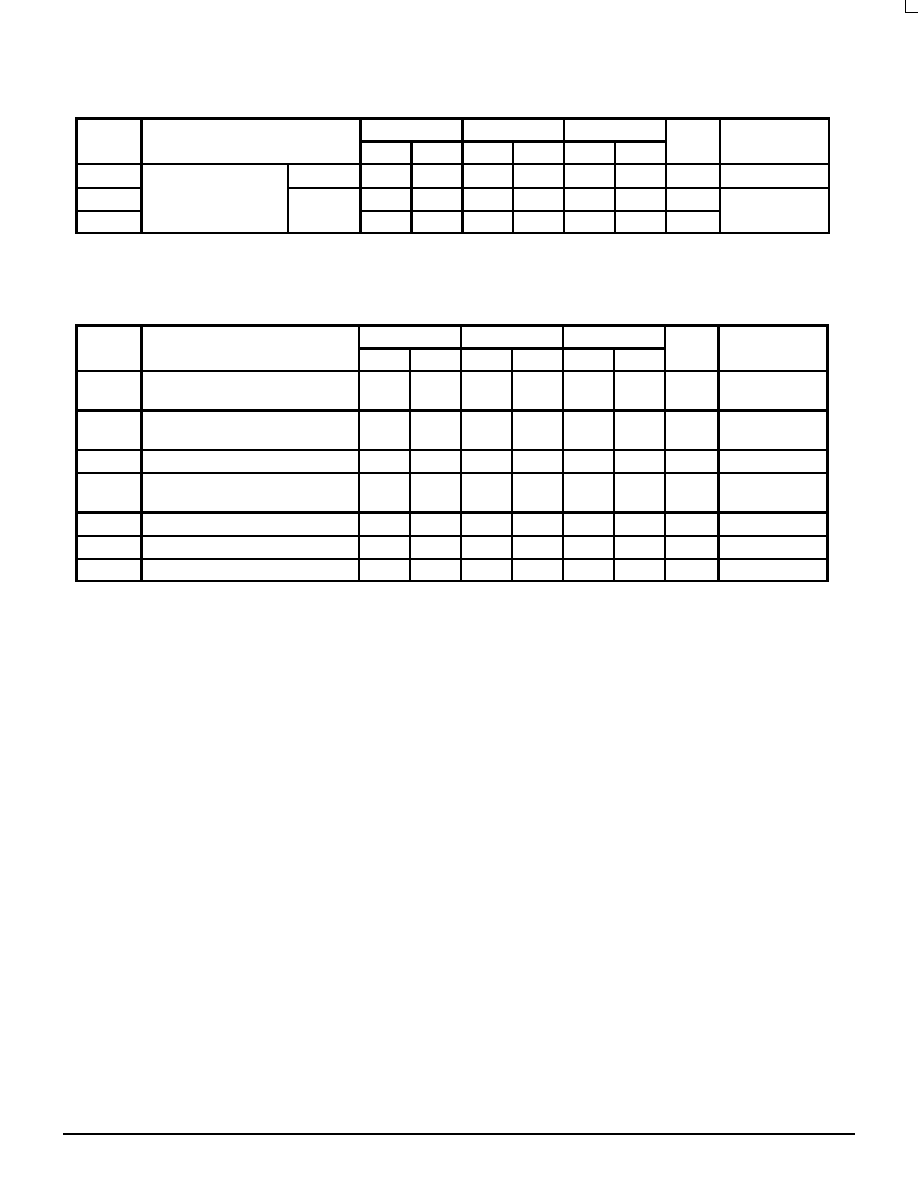
10H PECL CHARACTERISTICS (VT = VE = 5.0V
▒
5%)
TA = 0
░
C
TA = 25
░
C
TA = 85
░
C
Symbol
Characteristic
Min
Max
Min
Max
Min
Max
Unit
Condition
IIH
IIL
Input HIGH Current
Input LOW Current
0.5
225
0.5
175
0.5
175
╡
A
* NOTE
VIH
VIL
Input HIGH Voltage
Input LOW Voltage
3.83
3.05
4.16
3.52
3.87
3.05
4.19
3.52
3.94
3.05
4.28
3.555
V
VEE = 5.0V
* NOTE
VBB
Output Reference Voltage
3.62
3.73
3.65
3.75
3.69
3.81
V
100H PECL CHARACTERISTICS (VT = VE = 5.0V
▒
5%)
TA = 0
░
C
TA = 25
░
C
TA = 85
░
C
Symbol
Characteristic
Min
Max
Min
Max
Min
Max
Unit
Condition
IIH
IIL
Input HIGH Current
Input LOW Current
0.5
225
0.5
175
0.5
175
╡
A
* NOTE
VIH
VIL
Input HIGH Voltage
Input LOW Voltage
3.835
3.190
4.120
3.525
3.835
3.190
4.120
3.525
3.835
3.190
4.120
3.525
V
VEE = 5.0V
* NOTE
VBB
Output Reference Voltage
3.620
3.740
3.620
3.740
3.620
3.740
V
*NOTE: PECL LEVELS are referenced to VCC and will vary 1:1 with the power supply. The VALUES shown are for VCC = 5.0V.
MC10H642 MC100H642
MOTOROLA
MECL Data
DL122 -- Rev 6
2н4
10H/100H DC CHARACTERISTICS (VT = VE = 5.0V
▒
5%)
TA = 0
░
C
TA = 25
░
C
TA = 85
░
C
Symbol
Characteristic
Min
Max
Min
Max
Min
Max
Unit
Condition
IEE
Power Supply Current
PECL
57
57
57
mA
VE Pin
ICCH
TTL
30
30
30
mA
Total All VT Pins
ICCL
30
30
30
mA
10H/100H TTL DC CHARACTERISTICS (VT = VE = 5.0V
▒
5%)
TA = 0
░
C
TA = 25
░
C
TA = 85
░
C
Symbol
Characteristic
Min
Max
Min
Max
Min
Max
Unit
Condition
VIH
VIL
Input HIGH Voltage
Input LOW Voltage
2.0
0.8
2.0
0.8
2.0
0.8
V
IIH
Input HIGH Current
20
100
20
100
20
100
╡
A
VIN = 2.7V
VIN = 7.0V
IIL
Input LOW Current
н0.6
н0.6
н0.6
mA
VIN = 0.5V
VOH
Output HIGH Voltage
2.5
2.0
2.5
2.0
2.5
2.0
V
IOH = н3.0mA
IOH = н15mA
VOL
Output LOW Voltage
0.5
0.5
0.5
V
IOL = 24mA
VIK
Input Clamp Voltage
н1.2
н1.2
н1.2
V
IIN = н18mA
IOS
Output Short Circuit Current
н100
н225
н100
н225
н100
н225
mA
VOUT = 0V
10/100H642
DUTY CYCLE CONTROL
To maintain a duty cycle of
▒
5% at 50 MHz, limit the load capacitance and/or power supply variation as shown in Figures 1 and 2.
For a
▒
2.5% duty cycle limit, see Figures 3 and 4. Figures 5 and 6 show duty cycle variation with temperature. Figure 7 shows typical
TPD versus load. Figure 8 shows reset recovery time. Figure 9 shows output states after power up.
Best duty cycle control is obtained with a single
╡
P load and minimum line length.

MC10H642 MC100H642
2н5
MOTOROLA
MECL Data
DL122 -- Rev 6
Figure 1. MC10H642 Positive PW versus Load
@
▒
5% VCC, TA = 25
░
C
5.25
5.00
4.75
11
10
9
0
10
20
30
40
50
60
CAPACITIVE LOAD (pF)
POSITIVE PULSE WIDTH (ns)
CAPACITIVE LOAD (pF)
Figure 2. MC10H642 Negative PW versus
Load
@
▒
5% VCC, TA = 25
░
C
5.25
5.00
4.75
11
10
9
0
10
20
30
40
50
60
NEGA
TIVE PULSE WIDTH (ns)
CAPACITIVE LOAD (pF)
Figure 3. MC10H642 Positive PW versus Load
@
▒
2.5% VCC, TA = 25
░
C
5.125
5.00
4.875
10.6
10.4
10.2
10.0
9.8
9.6
9.4
9.2
0
10
20
30
40
50
60
POSITIVE PULSE WIDTH (ns)
CAPACITIVE LOAD (pF)
Figure 4. MC10H642 Negative PW versus Load
@
▒
2.5% VCC, TA = 25
░
C
5.125
5.00
4.875
10.8
10.6
10.4
10.2
10.0
9.8
9.6
9.4
0
10
20
30
40
50
60
NEGA
TIVE PULSE WIDTH (ns)
TEMPERATURE (
░
C)
Figure 5. MC10H642 Positive PW versus Temperature,
VCC = 5.0V
50 pF
25 pF
0 pF
10.4
10.2
10.0
9.8
9.6
9.4
0
20
40
60
80
100
POSITIVE PULSE WIDTH (ns)
Figure 6. MC10H642 Negative PW versus
Temperature, VCC = 5.0V
50 pF
25 pF
0 pF
10.5
10.3
10.1
9.9
9.7
9.5
0
20
40
60
80
100
TEMPERATURE (
░
C)
NEGA
TIVE PULSE WIDTH (ns)