 | –≠–ª–µ–∫—Ç—Ä–æ–Ω–Ω—ã–π –∫–æ–º–ø–æ–Ω–µ–Ω—Ç: MC145170 | –°–∫–∞—á–∞—Ç—å:  PDF PDF  ZIP ZIP |

MC145170≠1
MOTOROLA
1
Advance Information
PLL Frequency Synthesizer
with Serial Interface
CMOS
The new MC145170≠1 is pin≠for≠pin compatible with the MC145170. A
comparison of the two parts is shown in the table below. The MC145170≠1 is
recommended for new designs.
The MC145170≠1 is a single≠chip synthesizer capable of direct usage in the
MF, HF, and VHF bands. A special architecture makes this PLL the easiest to
program in the industry. Either a bit≠ or byte≠oriented format may be used. Due
to the patented BitGrabber
TM
registers, no address/steering bits are required for
random access of the three registers. Thus, tuning can be accomplished via a
2≠byte serial transfer to the 16≠bit N register.
The device features fully programmable R and N counters, an amplifier at the
fin pin, on≠chip support of an external crystal, a programmable reference
output, and both single≠ and double≠ended phase detectors with linear transfer
functions (no dead zones). A configuration (C) register allows the part to be
configured to meet various applications. A patented feature allows the C
register to shut off unused outputs, thereby minimizing noise and interference.
In order to reduce lock times and prevent erroneous data from being loaded
into the counters, a patented jam≠load feature is included. Whenever a new
divide ratio is loaded into the N register, both the N and R counters are
jam≠loaded with their respective values and begin counting down together. The
phase detectors are also initialized during the jam load.
∑
Operating Voltage Range: 2.5 to 5.5 V
∑
Maximum Operating Frequency:
185 MHz @ Vin = 500 mV p≠p, 4.5 V Minimum Supply
100 MHz @ Vin = 500 mV p≠p, 3.0 V Minimum Supply
∑
Operating Supply Current:
0.6 mA @ 3 V, 30 MHz
1.5 mA @ 3 V, 100 MHz
3.0 mA @ 5 V, 50 MHz
5.8 mA @ 5 V, 185 MHz
∑
Operating Temperature Range: ≠ 40 to 85
∞
C
∑
R Counter Division Range: 1 and 5 to 32,767
∑
N Counter Division Range: 40 to 65,535
∑
Direct Interface to Motorola SPI and National MICROWIRE
TM
Serial Data
Ports
∑
Chip Complexity: 4800 FETs or 1200 Equivalent Gates
∑
See Application Note AN1207/D
COMPARISION OF THE PLL FREQUENCY SYNTHESIZERS
Parameter
MC145170≠1
MC145170
Technology
1.2
µ
m CMOS
1.5
µ
m CMOS
Maximum Frequency with 5 V
±
10% Supply, fin
185 MHz
160 MHz
Maximum Frequency with 5 V
±
10% Supply, OSCin
25 MHz
20 MHz
Maximum Supply Voltage
5.5 V
6.0 V
Maximum Input Capacitance, fin
7 pF
5 pF
This document contains information on a new product. Specifications and information herein are subject to change without notice.
BitGrabber is a trademark of Motorola Inc. MICROWIRE is a trademark of National Semiconductor Corp.
Order this document
by MC145170≠1/D
MOTOROLA
SEMICONDUCTOR TECHNICAL DATA
MC145170-1
fR
LD
VSS
9
10
11
12
V
VDD
PDout
8
7
6
5
4
3
2
1
Dout
CLK
ENB
fin
REFout
OSCout
OSCin
14
15
16
PIN ASSIGNMENT
Din
fV
P SUFFIX
PLASTIC DIP
CASE 648
D SUFFIX
SOG PACKAGE
CASE 751B
ORDERING INFORMATION
MC145170P1
Plastic DIP
MC145170D1
SOG Package
MC145170DT1 TSSOP
R
16
1
13
DT SUFFIX
TSSOP
CASE 948C
16
1
16
1
©
Motorola, Inc. 1996
REV 1
3/96

MC145170≠1
MOTOROLA
2
BLOCK DIAGRAM
ENB
OSCin
Din
CLK
OSCout
fin
OSC
1
2
7
5
4
INPUT
AMP
3
15
16
15≠STAGE R COUNTER
16≠STAGE N COUNTER
SHIFT
REGISTER
AND
CONTROL
LOGIC
POR
BitGrabber N REGISTER
16 BITS
BitGrabber C REGISTER
8 BITS
BitGrabber R REGISTER
15 BITS
PHASE/FREQUENCY
DETECTOR B AND CONTROL
PHASE/FREQUENCY
DETECTOR A AND CONTROL
LOCK DETECTOR
AND CONTROL
16
LD
PDout
R
V
10
15
14
13
11
9
PIN 16 = VDD
PIN 12 = VSS
6
4≠STAGE
REFERENCE
DIVIDER
REFout
3
Dout
8
fV CONTROL
fR CONTROL
fR
fV
MAXIMUM RATINGS*
(Voltages Referenced to VSS)
Symbol
Parameter
Value
Unit
VDD
DC Supply Voltage
≠ 0.5 to + 5.5
V
Vin
DC Input Voltage
≠ 0.5 to VDD + 0.5
V
Vout
DC Output Voltage
≠ 0.5 to VDD + 0.5
V
Iin
DC Input Current, per Pin
±
10
mA
Iout
DC Output Current, per Pin
±
20
mA
IDD
DC Supply Current, VDD and VSS Pins
±
30
mA
PD
Power Dissipation, per Package
300
mW
Tstg
Storage Temperature
≠ 65 to + 150
∞
C
TL
Lead Temperature, 1 mm from Case
for 10 seconds
260
∞
C
* Maximum Ratings are those values beyond which damage to the device may occur.
Functional operation should be restricted to the limits in the Electrical Characteristics
tables or Pin Descriptions section.
This device contains protection circuitry to
guard against damage due to high static
voltages or electric fields. However, pre-
cautions must be taken to avoid applications of
any voltage higher than maximum rated volt-
ages to this high≠impedance circuit. For proper
operation, Vin and Vout should be constrained
to the range VSS
(Vin or Vout)
VDD.
Unused inputs must always be tied to an
appropriate logic voltage level (e.g., either VSS
or VDD). Unused outputs must be left open.
MC145170≠1
MOTOROLA
3
ELECTRICAL CHARACTERISTICS
(Voltages Referenced to VSS, TA = ≠ 40 to + 85
∞
C)
Symbol
Parameter
Test Condition
VDD
V
Guaranteed
Limit
Unit
VDD
Power Supply Voltage Range
--
2.5 to 5.5
V
VIL
Maximum Low≠Level Input Voltage*
(Din, CLK, ENB, fin)
dc Coupling to fin
2.5
4.5
5.5
0.50
1.35
1.65
V
VIH
Minimum High≠Level Input Voltage*
(Din, CLK, ENB, fin)
dc Coupling to fin
2.5
4.5
5.5
2.00
3.15
3.85
V
VHys
Minimum Hysteresis Voltage (CLK, ENB)
2.5
5.5
0.15
0.20
V
VOL
Maximum Low≠Level Output Voltage
(Any Output)
Iout = 20
µ
A
2.5
5.5
0.1
0.1
V
VOH
Minimum High≠Level Output Voltage
(Any Output)
Iout = ≠ 20
µ
A
2.5
5.5
2.4
5.4
V
IOL
Minimum Low≠Level Output Current
(PDout, REFout, fR, fV, LD,
R,
V)
Vout = 0.3 V
Vout = 0.4 V
Vout = 0.5 V
2.5
4.5
5.5
0.12
0.36
0.36
mA
IOH
Minimum High≠Level Output Current
(PDout, REFout, fR, fV, LD,
R,
V)
Vout = 2.2 V
Vout = 4.1 V
Vout = 5.0 V
2.5
4.5
5.5
≠ 0.12
≠ 0.36
≠ 0.36
mA
IOL
Minimum Low≠Level Output Current
(Dout)
Vout = 0.4 V
4.5
1.6
mA
IOH
Minimum High≠Level Output Current
(Dout)
Vout = 4.1 V
4.5
≠ 1.6
mA
Iin
Maximum Input Leakage Current
(Din, CLK, ENB, OSCin)
Vin = VDD or VSS
5.5
±
1.0
µ
A
Iin
Maximum Input Current
(fin)
Vin = VDD or VSS
5.5
±
120
µ
A
IOZ
Maximum Output Leakage Current (PDout) Vin = VDD or VSS,
Output in High≠Impedance State
5.5
±
100
nA
(Dout)
5.5
±
5
µ
A
IDD
Maximum Quiescent Supply Current
Vin = VDD or VSS; Outputs Open;
Excluding fin Amp Input Current Component
5.5
100
µ
A
Idd
Maximum Operating Supply Current
fin = 500 mV p≠p;
OSCin = 1 MHz @ 1 V p≠p;
LD, fR, fV, REFout = Inactive and No Connect;
OSCout,
V,
R, PDout = No Connect;
Din, ENB, CLK = VDD or VSS
--
**
mA
* When dc coupling to the OSCin pin is used, the pin must be driven rail≠to≠rail. In this case, OSCout should be floated.
** The nominal values at 3 V are 0.6 mA @ 30 MHz, and 1.5 mA @ 100 MHz. The nominal values at 5 V are 3.0 mA @ 50 MHz, and 5.8 mA
@ 185 MHz. These are not guaranteed limits.
MC145170≠1
MOTOROLA
4
AC INTERFACE CHARACTERISTICS
( TA = ≠ 40 to + 85
∞
C, CL = 50 pF, Input tr = tf = 10 ns unless otherwise indicated)
Symbol
Parameter
Figure
No.
VDD
V
Guaranteed
Limit
Unit
fclk
Serial Data Clock Frequency (Note: Refer to Clock tw Below)
1
2.5
4.5
5.5
dc to 3.0
dc to 4.0
dc to 4.0
MHz
tPLH, tPHL
Maximum Propagation Delay, CLK to Dout
1, 5
2.5
4.5
5.5
150
85
85
ns
tPLZ, tPHZ
Maximum Disable Time, Dout Active to High Impedance
2, 6
2.5
4.5
5.5
300
200
200
ns
tPZL, tPZH
Access Time, Dout High Impedance to Active
2, 6
2.5
4.5
5.5
0 to 200
0 to 100
0 to 100
ns
tTLH, tTHL
Maximum Output Transition Time, Dout
CL = 50 pF
1, 5
2.5
4.5
5.5
150
50
50
ns
CL = 200 pF
1, 5
2.5
4.5
5.5
900
150
150
ns
Cin
Maximum Input Capacitance ≠ Din, ENB, CLK
--
10
pF
Cout
Maximum Output Capacitance ≠ Dout
--
10
pF
TIMING REQUIREMENTS
( TA = ≠ 40 to + 85
∞
C, Input tr = tf = 10 ns unless otherwise indicated)
Symbol
Parameter
Figure
No.
VDD
V
Guaranteed
Limit
Unit
tsu, th
Minimum Setup and Hold Times, Din vs CLK
3
2.5
4.5
5.5
55
40
40
ns
tsu, th, trec
Minimum Setup, Hold, and Recovery Times, ENB vs CLK
4
2.5
4.5
5.5
135
100
100
ns
tw(H)
Minimum Inactive≠High Pulse Width, ENB
4
2.5
4.5
5.5
400
300
300
ns
tw
Minimum Pulse Width, CLK
1
2.5
4.5
5.5
166
125
125
ns
tr, tf
Maximum Input Rise and Fall Times, CLK
1
2.5
4.5
5.5
100
100
100
µ
s
MC145170≠1
MOTOROLA
5
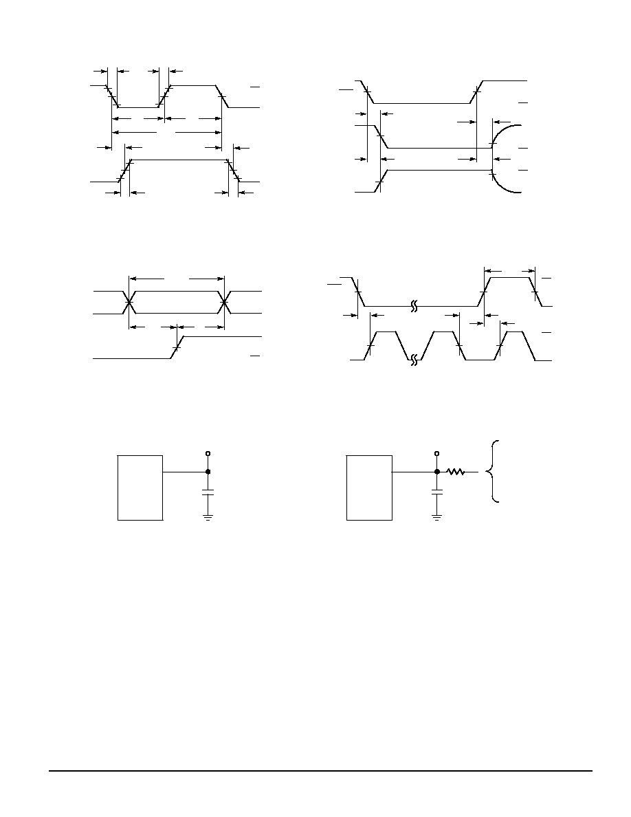
SWITCHING WAVEFORMS
10%
VDD
VSS
1/fclk
Dout
CLK
90%
50%
90%
50%
10%
tPLH
tPHL
tTLH
tTHL
tw
tw
tf
tr
Figure 1.
ENB
Dout
Dout
50%
VDD
VSS
50%
tPZH
tPZL
tPLZ
50%
tPHZ
Figure 2.
10%
90%
VDD
VSS
HIGH
IMPEDANCE
HIGH
IMPEDANCE
Din
CLK
50%
VALID
50%
tsu
th
VDD
VSS
VDD
VSS
Figure 3.
CLK
ENB
50%
tsu
th
FIRST
CLK
LAST
CLK
trec
50%
Figure 4.
VDD
VSS
VDD
VSS
tw(H)
TEST POINT
DEVICE
UNDER
TEST
CL
*
* Includes all probe and fixture capacitance.
Figure 5. Test Circuit
TEST POINT
DEVICE
UNDER
TEST
CL
*
* Includes all probe and fixture capacitance.
Figure 6. Test Circuit
7.5 k
CONNECT TO VDD
WHEN TESTING tPLZ
AND tPZL. CONNECT TO
VSS WHEN TESTING
tPHZ AND tPZH.