 | –≠–ª–µ–∫—Ç—Ä–æ–Ω–Ω—ã–π –∫–æ–º–ø–æ–Ω–µ–Ω—Ç: MC14538B | –°–∫–∞—á–∞—Ç—å:  PDF PDF  ZIP ZIP |
MOTOROLA CMOS LOGIC DATA
1
MC14538B
Dual Precision
Retriggerable/Resettable
Monostable Multivibrator
The MC14538B is a dual, retriggerable, resettable monostable multivibra-
tor. It may be triggered from either edge of an input pulse, and produces an
accurate output pulse over a wide range of widths, the duration and accuracy
of which are determined by the external timing components, CX and RX.
∑
Unlimited Rise and Fall Time Allowed on the A Trigger Input
∑
Pulse Width Range = 10
µ
s to 10 s
∑
Latched Trigger Inputs
∑
Separate Latched Reset Inputs
∑
3.0 Vdc to 18 Vdc Operational Limits
∑
Triggerable from Positive (A Input) or Negative≠Going Edge (B≠Input)
∑
Capable of Driving Two Low≠power TTL Loads or One Low≠power
Schottky TTL Load Over the Rated Temperature Range
∑
Pin≠for≠pin Compatible with MC14528B and CD4528B (CD4098)
∑
Use the MC54/74HC4538A for Pulse Widths Less Than 10
µ
s with
Supplies Up to 6 V.
ŒŒŒŒŒŒŒŒŒŒŒŒŒŒŒŒŒŒŒŒŒ
ŒŒŒŒŒŒŒŒŒŒŒŒŒŒŒŒŒŒŒŒŒ
ŒŒŒŒŒŒŒŒŒŒŒŒŒŒŒŒŒŒŒŒŒ
ŒŒŒŒŒŒŒŒŒŒŒŒŒŒŒŒŒŒŒŒŒ
MAXIMUM RATINGS*
(Voltages Referenced to VSS)
ŒŒŒŒ
ŒŒŒŒ
ŒŒŒŒ
ŒŒŒŒ
Symbol
ŒŒŒŒŒŒŒŒŒŒŒ
ŒŒŒŒŒŒŒŒŒŒŒ
ŒŒŒŒŒŒŒŒŒŒŒ
ŒŒŒŒŒŒŒŒŒŒŒ
Parameter
ŒŒŒŒŒŒ
ŒŒŒŒŒŒ
ŒŒŒŒŒŒ
ŒŒŒŒŒŒ
Value
ŒŒŒ
ŒŒŒ
ŒŒŒ
ŒŒŒ
Unit
ŒŒŒŒ
ŒŒŒŒ
ŒŒŒŒ
ŒŒŒŒ
VDD
ŒŒŒŒŒŒŒŒŒŒŒ
ŒŒŒŒŒŒŒŒŒŒŒ
ŒŒŒŒŒŒŒŒŒŒŒ
ŒŒŒŒŒŒŒŒŒŒŒ
DC Supply Voltage
ŒŒŒŒŒŒ
ŒŒŒŒŒŒ
ŒŒŒŒŒŒ
ŒŒŒŒŒŒ
≠ 0.5 to + 18.0
ŒŒŒ
ŒŒŒ
ŒŒŒ
ŒŒŒ
V
ŒŒŒŒ
ŒŒŒŒ
ŒŒŒŒ
Vin, Vout
ŒŒŒŒŒŒŒŒŒŒŒ
ŒŒŒŒŒŒŒŒŒŒŒ
ŒŒŒŒŒŒŒŒŒŒŒ
Input or Output Voltage (DC or Transient)
ŒŒŒŒŒŒ
ŒŒŒŒŒŒ
ŒŒŒŒŒŒ
≠ 0.5 to VDD + 0.5
ŒŒŒ
ŒŒŒ
ŒŒŒ
V
ŒŒŒŒ
ŒŒŒŒ
ŒŒŒŒ
ŒŒŒŒ
ŒŒŒŒ
Iin, Iout
ŒŒŒŒŒŒŒŒŒŒŒ
ŒŒŒŒŒŒŒŒŒŒŒ
ŒŒŒŒŒŒŒŒŒŒŒ
ŒŒŒŒŒŒŒŒŒŒŒ
ŒŒŒŒŒŒŒŒŒŒŒ
Input or Output Current (DC or Transient),
per Pin
ŒŒŒŒŒŒ
ŒŒŒŒŒŒ
ŒŒŒŒŒŒ
ŒŒŒŒŒŒ
ŒŒŒŒŒŒ
±
10
ŒŒŒ
ŒŒŒ
ŒŒŒ
ŒŒŒ
ŒŒŒ
mA
ŒŒŒŒ
ŒŒŒŒ
ŒŒŒŒ
ŒŒŒŒ
PD
ŒŒŒŒŒŒŒŒŒŒŒ
ŒŒŒŒŒŒŒŒŒŒŒ
ŒŒŒŒŒŒŒŒŒŒŒ
ŒŒŒŒŒŒŒŒŒŒŒ
Power Dissipation, per Package
ŒŒŒŒŒŒ
ŒŒŒŒŒŒ
ŒŒŒŒŒŒ
ŒŒŒŒŒŒ
500
ŒŒŒ
ŒŒŒ
ŒŒŒ
ŒŒŒ
mW
ŒŒŒŒ
ŒŒŒŒ
ŒŒŒŒ
ŒŒŒŒ
Tstg
ŒŒŒŒŒŒŒŒŒŒŒ
ŒŒŒŒŒŒŒŒŒŒŒ
ŒŒŒŒŒŒŒŒŒŒŒ
ŒŒŒŒŒŒŒŒŒŒŒ
Storage Temperature
ŒŒŒŒŒŒ
ŒŒŒŒŒŒ
ŒŒŒŒŒŒ
ŒŒŒŒŒŒ
≠ 65 to + 150
ŒŒŒ
ŒŒŒ
ŒŒŒ
ŒŒŒ
_
C
ŒŒŒŒ
ŒŒŒŒ
ŒŒŒŒ
ŒŒŒŒ
TL
ŒŒŒŒŒŒŒŒŒŒŒ
ŒŒŒŒŒŒŒŒŒŒŒ
ŒŒŒŒŒŒŒŒŒŒŒ
ŒŒŒŒŒŒŒŒŒŒŒ
Lead Temperature (8≠Second Soldering)
ŒŒŒŒŒŒ
ŒŒŒŒŒŒ
ŒŒŒŒŒŒ
ŒŒŒŒŒŒ
260
ŒŒŒ
ŒŒŒ
ŒŒŒ
ŒŒŒ
_
C
* Maximum Ratings are those values beyond which damage to the device may occur.
Temperature Derating:
Plastic "P and D/DW" Packages: ≠ 7.0 mW/
_
C From 65
_
C To 125
_
C
Ceramic "L" Packages: ≠ 12 mW/
_
C From 100
_
C To 125
_
C
ONE≠SHOT SELECTION GUIDE
100 ns
MC14528B
MC14536B
MC14538B
MC14541B
MC4538A*
1
µ
s
10
µ
s
100
µ
s
1 ms
10 ms
100 ms
1 s
10 s
*LIMITED OPERATING VOLTAGE (2 ≠ 6 V)
TOTAL OUTPUT PULSE WIDTH RANGE
RECOMMENDED PULSE WIDTH RANGE
23 HR
5 MIN.
MOTOROLA
SEMICONDUCTOR TECHNICAL DATA
©
Motorola, Inc. 1995
REV 3
1/94
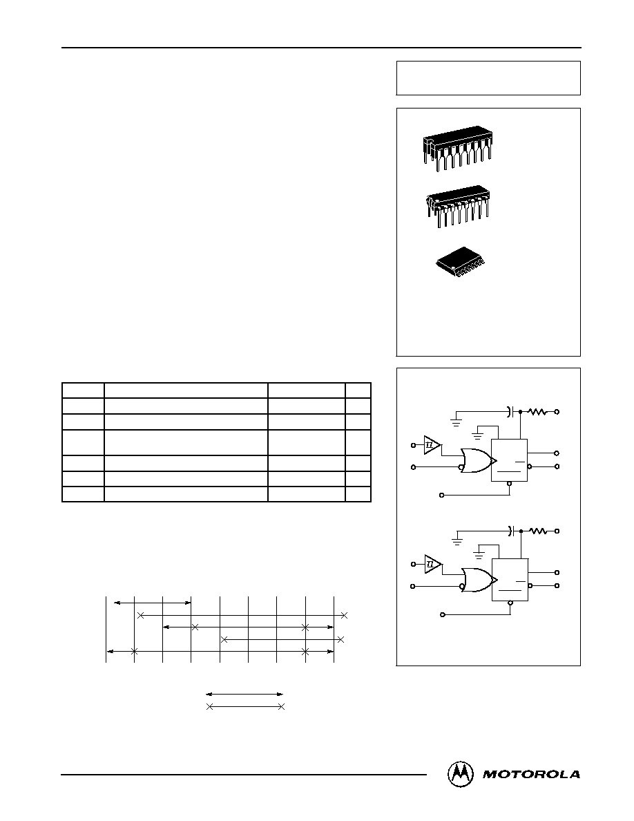
MC14538B
L SUFFIX
CERAMIC
CASE 620
ORDERING INFORMATION
MC14XXXBCP
Plastic
MC14XXXBCL
Ceramic
*MC14XXXBDW
SOIC
TA = ≠ 55
∞
to 125
∞
C for all packages.
P SUFFIX
PLASTIC
CASE 648
DW SUFFIX
SOIC
CASE 751G
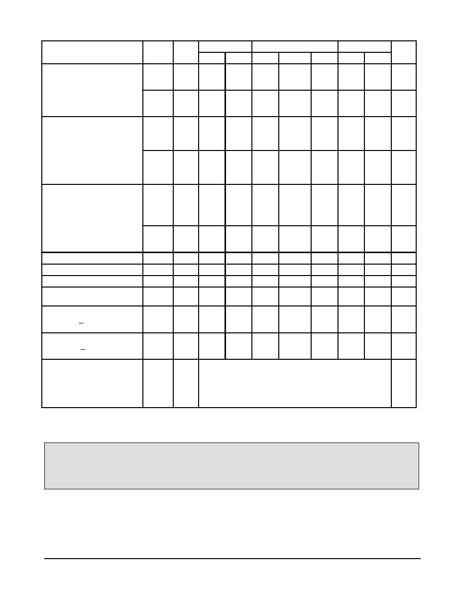
BLOCK DIAGRAM
* Consult factory for possible "D" suffix SOIC
Case 751B.
VDD
VDD
6
7
10
9
12
11
5
4
A
B
CX
RX
1
2
Q1
Q1
RESET
3
CX
RX
15
14
Q2
Q2
RESET
13
A
B
RX AND CX ARE EXTERNAL COMPONENTS.
VDD = PIN 16
VSS = PIN 8, PIN 1, PIN 15
MOTOROLA CMOS LOGIC DATA
MC14538B
2
ŒŒŒŒŒŒŒŒŒŒŒŒŒŒŒŒŒŒŒŒŒŒŒŒŒŒŒŒŒŒŒŒŒŒ
ŒŒŒŒŒŒŒŒŒŒŒŒŒŒŒŒŒŒŒŒŒŒŒŒŒŒŒŒŒŒŒŒŒŒ
ŒŒŒŒŒŒŒŒŒŒŒŒŒŒŒŒŒŒŒŒŒŒŒŒŒŒŒŒŒŒŒŒŒŒ
ŒŒŒŒŒŒŒŒŒŒŒŒŒŒŒŒŒŒŒŒŒŒŒŒŒŒŒŒŒŒŒŒŒŒ
ELECTRICAL CHARACTERISTICS
(Voltages Referenced to VSS)
Characteristic
Symbol
VDD
Vdc
≠ 55
_
C
25
_
C
125
_
C
Unit
Characteristic
Symbol
DD
Vdc
Min
Max
Min
Typ #
Max
Min
Max
Unit
Output Voltage
"0" Level
Vin = VDD or 0
VOL
5.0
10
15
--
--
--
0.05
0.05
0.05
--
--
--
0
0
0
0.05
0.05
0.05
--
--
--
0.05
0.05
0.05
Vdc
"1" Level
Vin = 0 or VDD
VOH
5.0
10
15
4.95
9.95
14.95
--
--
--
4.95
9.95
14.95
5.0
10
15
--
--
--
4.95
9.95
14.95
--
--
--
Vdc
Input Voltage
"0" Level
(VO = 4.5 or 0.5 Vdc)
(VO = 9.0 or 1.0 Vdc)
(VO = 13.5 or 1.5 Vdc)
VIL
5.0
10
15
--
--
--
1.5
3.0
4.0
--
--
--
2.25
4.50
6.75
1.5
3.0
4.0
--
--
--
1.5
3.0
4.0
Vdc
"1" Level
(VO = 0.5 or 4.5 Vdc)
(VO = 1.0 or 9.0 Vdc)
(VO = 1.5 or 13.5 Vdc)
VIH
5.0
10
15
3.5
7.0
11
--
--
--
3.5
7.0
11
2.75
5.50
8.25
--
--
--
3.5
7.0
11
--
--
--
Vdc
Output Drive Current
(VOH = 2.5 Vdc)
Source
(VOH = 4.6 Vdc)
(VOH = 9.5 Vdc)
(VOH = 13.5 Vdc)
IOH
5.0
5.0
10
15
≠ 3.0
≠ 0.64
≠ 1.6
≠ 4.2
--
--
--
--
≠ 2.4
≠ 0.51
≠ 1.3
≠ 3.4
≠ 4.2
≠ 0.88
≠ 2.25
≠ 8.8
--
--
--
--
≠ 1.7
≠ 0.36
≠ 0.9
≠ 2.4
--
--
--
--
mAdc
(VOL = 0.4 Vdc)
Sink
(VOL = 0.5 Vdc)
(VOL = 1.5 Vdc)
IOL
5.0
10
15
0.64
1.6
4.2
--
--
--
0.51
1.3
3.4
0.88
2.25
8.8
--
--
--
0.36
0.9
2.4
--
--
--
mAdc
Input Current, Pin 2 or 14
Iin
15
--
±
0.05
--
±
0.00001
±
0.05
--
±
0.5
µ
Adc
Input Current, Other Inputs
Iin
15
--
±
0.1
--
±
0.00001
±
0.1
--
±
1.0
µ
Adc
Input Capacitance, Pin 2 or 14
Cin
--
--
--
--
25
--
--
--
pF
Input Capacitance, Other Inputs
(Vin = 0)
Cin
--
--
--
--
5.0
7.5
--
--
pF
Quiescent Current
(Per Package)
Q = Low, Q = High
IDD
5.0
10
15
--
--
--
5.0
10
20
--
--
--
0.005
0.010
0.015
5.0
10
20
--
--
--
150
300
600
µ
Adc
Quiescent Current, Active State
(Both) (Per Package)
Q = High, Q = Low
IDD
5.0
10
15
--
--
--
2.0
2.0
2.0
--
--
--
0.04
0.08
0.13
0.20
0.45
0.70
--
--
--
2.0
2.0
2.0
mAdc
**Total Supply Current at an
external load capacitance (CL) and
at external timing network (RX, CX)
IT
5.0
10
IT = (3.5 x 10≠2) RXCXf + 4CXf + 1 x 10≠5 CLf
IT = (8.0 x 10≠2) RXCXf + 9CXf + 2 x 10≠5 CLf
IT = (1.25 x 10≠1) RXCXf + 12CXf + 3 x 10≠5 CLf
where: IT in
µ
A (one monostable switching only),
where:
CX in
µ
F, CL in pF, RX in k ohms, and
where:
f in Hz is the input frequency.
µ
Adc
#Data labelled "Typ" is not to be used for design purposes but is intended as an indication of the IC's potential performance.
** The formulas given are for the typical characteristics only at 25
_
C.
This device contains protection circuitry to guard against damage due to high static voltages or electric fields. However,
precautions must be taken to avoid applications of any voltage higher than maximum rated voltages to this high-impedance
circuit. For proper operation, Vin and Vout should be constrained to the range VSS
(Vin or Vout)
VDD.
Unused inputs must always be tied to an appropriate logic voltage level (e.g., either VSS or VDD). Unused outputs must
be left open.
MOTOROLA CMOS LOGIC DATA
3
MC14538B
ŒŒŒŒŒŒŒŒŒŒŒŒŒŒŒŒŒŒŒŒŒŒŒŒŒŒŒŒŒŒŒŒŒŒ
ŒŒŒŒŒŒŒŒŒŒŒŒŒŒŒŒŒŒŒŒŒŒŒŒŒŒŒŒŒŒŒŒŒŒ
ŒŒŒŒŒŒŒŒŒŒŒŒŒŒŒŒŒŒŒŒŒŒŒŒŒŒŒŒŒŒŒŒŒŒ
ŒŒŒŒŒŒŒŒŒŒŒŒŒŒŒŒŒŒŒŒŒŒŒŒŒŒŒŒŒŒŒŒŒŒ
SWITCHING CHARACTERISTICS*
(CL = 50 pF, TA = 25
_
C)
Characteristic
Symbol
VDD
Vdc
All Types
Unit
Characteristic
Symbol
VDD
Vdc
Min
Typ #
Max
Unit
Output Rise Time
tTLH = (1.35 ns/pF) CL + 33 ns
tTLH = (0.60 ns/pF) CL + 20 ns
tTLH = (0.40 ns/pF) CL + 20 ns
tTLH
5.0
10
15
--
--
--
100
50
40
200
100
80
ns
Output Fall Time
tTHL = (1.35 ns/pF) CL + 33 ns
tTHL = (0.60 ns/pF) CL + 20 ns
tTHL = (0.40 ns/pF) CL + 20 ns
tTHL
5.0
10
15
--
--
--
100
50
40
200
100
80
ns
Propagation Delay Time
A or B to Q or Q
tPLH, tPHL = (0.90 ns/pF) CL + 255 ns
tPLH, tPHL = (0.36 ns/pF) CL + 132 ns
tPLH, tPHL = (0.26 ns/pF) CL + 87 ns
tPLH,
tPHL
5.0
10
15
--
--
--
300
150
100
600
300
220
ns
Reset to Q or Q
tPLH, tPHL = (0.90 ns/pF) CL + 205 ns
tPLH, tPHL = (0.36 ns/pF) CL + 107 ns
tPLH, tPHL = (0.26 ns/pF) CL + 82 ns
5.0
10
15
--
--
--
250
125
95
500
250
190
ns
Input Rise and Fall Times
Reset
tr, tf
5
10
15
--
--
--
--
--
--
15
5
4
µ
s
B Input
5
10
15
--
--
--
300
1.2
0.4
1.0
0.1
0.05
ms
A Input
5
10
15
No Limit
--
Input Pulse Width
A, B, or Reset
tWH,
tWL
5.0
10
15
170
90
80
85
45
40
--
--
--
ns
Retrigger Time
trr
5.0
10
15
0
0
0
--
--
--
--
--
--
ns
Output Pulse Width -- Q or Q
Refer to Figures 8 and 9
CX = 0.002
µ
F, RX = 100 k
T
5.0
10
15
198
200
202
210
212
214
230
232
234
µ
s
CX = 0.1
µ
F, RX = 100 k
5.0
10
15
9.3
9.4
9.5
9.86
10
10.14
10.5
10.6
10.7
ms
CX = 10
µ
F, RX = 100 k
5.0
10
15
0.91
0.92
0.93
0.965
0.98
0.99
1.03
1.04
1.06
s
Pulse Width Match between circuits in
the same package.
CX = 0.1
µ
F, RX = 100 k
100
[(T1 ≠ T2)/T1]
5.0
10
15
--
--
--
±
1.0
±
1.0
±
1.0
±
5.0
±
5.0
±
5.0
%
* The formulas given are for the typical characteristics only at 25
_
C.
#Data labelled "Typ" is not to be used for design purposes but is intended as an indication of the IC's potential performance.
ŒŒŒŒŒŒŒŒŒŒŒŒŒŒŒŒŒŒŒŒŒŒŒŒŒŒŒŒŒŒŒŒŒŒ
ŒŒŒŒŒŒŒŒŒŒŒŒŒŒŒŒŒŒŒŒŒŒŒŒŒŒŒŒŒŒŒŒŒŒ
ŒŒŒŒŒŒŒŒŒŒŒŒŒŒŒŒŒŒŒŒŒŒŒŒŒŒŒŒŒŒŒŒŒŒ
ŒŒŒŒŒŒŒŒŒŒŒŒŒŒŒŒŒŒŒŒŒŒŒŒŒŒŒŒŒŒŒŒŒŒ
OPERATING CONDITIONS
External Timing Resistance
RX
--
5.0
--
k
External Timing Capacitance
CX
--
0
--
No
Limit
µ
F
* The maximum usable resistance RX is a function of the leakage of the capacitor CX, leakage of the MC14538B, and leakage due to board layout
and surface resistance. Susceptibility to externally induced noise signals may occur for RX > 1 M
..
If CX > 15
µ
F, use discharge protection diode per Fig. 11.
MOTOROLA CMOS LOGIC DATA
MC14538B
4
Figure 1. Logic Diagram
(1/2 of DevIce Shown)
NOTE: Pins 1, 8 and 15 must
be externally grounded
≠
+
≠
+
VDD
VDD
P1
RX
CX
2
1
(14)
(15)
4 (12)
5 (11)
3 (13)
A
B
RESET
VSS
N1
Vref1
C1
C2
ENABLE
Vref2
ENABLE
CONTROL
S
RESET LATCH
QR
QR
R
S
R
S
Q
Q
6 (10)
7 (9)
OUTPUT
LATCH
Figure 2. Power Dissipation Test Circuit and Waveforms
500 pF
VDD
0.1
µ
F
CERAMIC
RX
RX
CX
VSS
CX
VSS
Vin
CX/RX
A
B
RESET
A
B
RESET
Q
Q
Q
Q
VSS
CL
CL
CL
CL
20 ns
20 ns
VDD
0 V
90%
10%
Vin
ID
INPUT CONNECTIONS
Characteristics
Reset
A
B
tPLH, tPHL, tTLH, tTHL,
T, tWH, tWL
VDD
PG1
VDD
tPLH, tPHL, tTLH, tTHL,
T, tWH, tWL
VDD
VSS
PG2
tPLH(R), tPHL(R),
tWH, tWL
PG3
PG1
PG2
Figure 3. Switching Test Circuit
* Includes capacitance of probes,
wiring, and fixture parasitic.
NOTE: Switching test waveforms
for PG1, PG2, PG3 are shown
In Figure 4.
VDD
RX
RX
VSS
CX
CX/RX
A
B
RESET
A
B
RESET
Q
Q
Q
Q
CL
CX
CL
CL
CL
VSS
PULSE
GENERATOR
PULSE
GENERATOR
PULSE
GENERATOR
VSS
* CL = 50 pF
PG1 =
PG2 =
PG3 =
MOTOROLA CMOS LOGIC DATA
5
MC14538B
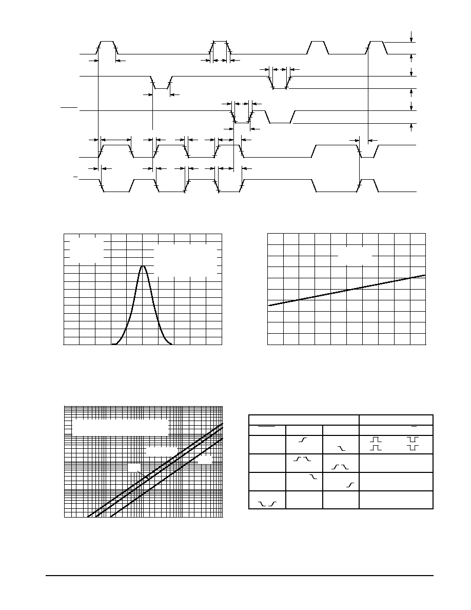
Figure 4. Switching Test Waveforms
RESET
A
B
tPLH
Q
Q
50%
tWH
90%
10%
tTLH
tTHL
tWL
tTHL
tPHL
tTHL
90%
10%
50%
T
50%
50%
50%
90%
10%
tPLH
tTHL
tTLH
tPHL
tWL
50%
90%
10%
tPHL tPHL
tTLH
tTHL
tPLH
50%
50%
90%
10%
50%
50%
50%
trr
50%
VDD
VDD
VDD
tTLH
Figure 5. Typical Normalized Distribution
of Units for Output Pulse Width
Figure 6. Typical Pulse Width Variation as
a Function of Supply Voltage VDD
0
0.2
0.4
0.6
0.8
1.0
≠ 4
≠ 2
0
2
4
T, OUTPUT PULSE WIDTH (%)
RELA
TIVE FREQUENCY
OF OCCURRENCE
2
1
0
1
2
15
14
13
12
11
10
9
8
7
6
5
VDD, SUPPLY VOLTAGE (VOLTS)
NORMALIZED PULSE WIDTH CHANGE
WITH RESPECT
T
O V
ALUE
A
T
V
DD
= 10 V (%)
TA = 25
∞
C
RX = 100 k
CX = 0.1
µ
F
0% POINT PULSE WIDTH
VDD = 5.0 V, T = 9.8 ms
VDD = 10 V, T = 10 ms
VDD = 15 V, T = 10.2 ms
RX = 100 k
CX = 0.1
µ
F
Figure 7. Typical Total Supply Current
versus Output Duty Cycle
T
OT
AL
SUPPL
Y
CURRENT
(
A)
µ
1000
100
10
1.0
0.1
0.001
0.1
1.0
10
100
OUTPUT DUTY CYCLE (%)
RX = 100 k
, CL = 50 pF
ONE MONOSTABLE SWITCHING ONLY
VDD = 15 V
10 V
5.0 V
FUNCTION TABLE
Inputs
Outputs
Reset
A
B
Q
Q
H
H
H
L
H
L
Not Triggered
H
H
Not Triggered
H
L, H,
H
Not Triggered
H
L
L, H,
Not Triggered
L
X
X
L
H
X
X
Not Triggered